Thermoelectric thin films based on conducting polymers
214
TECHNISCHE UNIVERSIT ¨ AT M ¨ UNCHEN Fakult¨atf¨ ur Physik Lehrstuhl f¨ ur Funktionelle Materialien Thermoelectric thin films based on conducting polymers Nitin Saxena, M. Sc. Vollst¨andiger Abdruck der von der Fakult¨ at f¨ ur Physik der Technischen Universit¨at M¨ unchen zur Erlangung des akademischen Grades eines Doktors der Naturwissenschaften (Dr. rer. nat.) genehmigten Dissertation. Vorsitzender: Prof. Dr. Andreas Weiler Pr¨ ufer der Dissertation: 1. Prof. Dr. Peter M¨ uller-Buschbaum 2. Prof. Dr. Martin Brandt Die Dissertation wurde am 20.02.2019 bei der Technischen Universit¨at M¨ unchen eingereicht und durch die Fakult¨ at f¨ ur Physik am 05.04.2019 angenommen.
-
Upload
khangminh22 -
Category
Documents
-
view
1 -
download
0
Transcript of Thermoelectric thin films based on conducting polymers

TECHNISCHE UNIVERSITAT MUNCHEN
Fakultat fur PhysikLehrstuhl fur Funktionelle Materialien
Thermoelectric thin films based onconducting polymers
Nitin Saxena, M. Sc.
Vollstandiger Abdruck der von der Fakultat fur Physik der Technischen UniversitatMunchen zur Erlangung des akademischen Grades eines
Doktors der Naturwissenschaften (Dr. rer. nat.)
genehmigten Dissertation.
Vorsitzender: Prof. Dr. Andreas WeilerPrufer der Dissertation: 1. Prof. Dr. Peter Muller-Buschbaum
2. Prof. Dr. Martin Brandt
Die Dissertation wurde am 20.02.2019 bei der Technischen Universitat Muncheneingereicht und durch die Fakultat fur Physik am 05.04.2019 angenommen.


Abstract
In this thesis, conducting polymer films are investigated regarding their potential appli-cation in thermoelectric thin films. Key parameters for the conversion efficiency of heatinto electricity are addressed and correlated with structural and optical properties. PE-DOT:PSS thin films are nanostructured with inorganic nanoparticles in order to reducethe thermal conductivity of the thin films. This is proven using infrared thermographyand explained with the help of resonant x-ray scattering. The intrinsically high chargecarrier concentration in PEDOT:PSS is systematically reduced with the help of inorganicsalts with acido-basic and redox properties in order to increase the Seebeck coefficient.The impact on electronic, compositional and conformational properties is observed withvarious spectroscopic techniques. Ionic liquids are used for post-treatment of PEDOT:PSSthin films, in order to simultaneously increase Seebeck coefficients and electrical conduc-tivities. The combined effect on electronic and structural properties is proven with thehelp of spectroscopy and x-ray scattering. P(NDI2OD-T2) is a popular representativeamong n-type polymers, and is doped with N-DPBI. The effect of doping on optical,structural and thermoelectric properties is assessed, and the obtained knowledge is usedfor the fabrication of a thermoelectric generator based on conducting polymers.
Zusammenfassung
In dieser Arbeit werden leitfahige Polymerfilme hinsichtlich ihrer potenziellen Anwen-dung in thermoelektrischen Dunnschichten untersucht. Fur die Umwandlung von Warmein Elektrizitat wichtige Parameter werden adressiert, und mit strukturellen und optis-chen Eigenschaften korreliert. Dunne PEDOT:PSS-Filme werden mithilfe von Silizium-Nanopartikeln nanostrukturiert, um die thermische Leitfahigkeit in Ersteren zu reduzieren.Dies wird mithilfe von Infrarot-Thermographie und resonanter Rontgenstreuung bewiesen.Die intrinsisch hohe Ladungstragerkonzentration in PEDOT:PSS wird mit anorganis-chen Salzen, welche Saure-Base- und Redox-Eigenschaften besitzen, gezielt reduziert umden Seebeck-Koeffizienten in diesen Filmen zu erhohen. Der Einfluss auf elektronis-che Eigenschaften, Zusammensetzung und Konformation wird mit verschiedenen spek-troskopischen Methoden untersucht. Ionische Flussigkeiten werden fur die Nachbehand-lung von PEDOT:PSS-Filmen eingesetzt, um simultan Seebeck-Koeffizienten und elek-trische Leitfahigkeiten zu erhohen. Der kombinierte Effekt auf elektronische und struk-turelle Eigenschaften wird mithilfe von optischer Spektroskopie und Rontgenstreuung be-wiesen. P(NDI2OD-T2) ist ein klassischer Vertreter der n-Typ-Polymere und wird mitN-DPBI dotiert. Das Dotieren wirkt sich auf optische, strukturelle und thermoelektrische

ii
Eigenschaften der Filme aus. Das erlangte Wissen wird dann benutzt um einen ther-moelektrischen Generator herzustellen, welcher auf leitfahigen Polymeren basiert.

Contents
Contents iii
List of abbreviations vii
1 Introduction 1
2 Theoretical background 72.1 Thermoelectric principles . . . . . . . . . . . . . . . . . . . . . . . . . . . . 7
2.1.1 Thermoelectric effects . . . . . . . . . . . . . . . . . . . . . . . . . 72.1.2 Thermoelectric figure of merit ZT . . . . . . . . . . . . . . . . . . . 10
2.2 Conducting polymers . . . . . . . . . . . . . . . . . . . . . . . . . . . . . . 122.2.1 Doping of conjugated polymers . . . . . . . . . . . . . . . . . . . . 142.2.2 PEDOT:PSS . . . . . . . . . . . . . . . . . . . . . . . . . . . . . . 172.2.3 P(NDI2OD-T2) . . . . . . . . . . . . . . . . . . . . . . . . . . . . . 19
2.3 Scattering basics . . . . . . . . . . . . . . . . . . . . . . . . . . . . . . . . 202.3.1 Grazing-incidence scattering . . . . . . . . . . . . . . . . . . . . . . 222.3.2 Grazing-incidence resonant tender x-ray scattering (GIR-TeXS) . . 24
3 Characterization methods 273.1 Thermoelectric characterization . . . . . . . . . . . . . . . . . . . . . . . . 27
3.1.1 Gradient chamber . . . . . . . . . . . . . . . . . . . . . . . . . . . . 273.1.2 XAVER: X-ray analysis voltage-emulation rig . . . . . . . . . . . . 293.1.3 4-point probe measurement . . . . . . . . . . . . . . . . . . . . . . 353.1.4 Surface profilometry . . . . . . . . . . . . . . . . . . . . . . . . . . 363.1.5 Infrared thermography (IRT) . . . . . . . . . . . . . . . . . . . . . 36
3.2 Spectroscopic characterization . . . . . . . . . . . . . . . . . . . . . . . . . 393.2.1 UV-Vis spectroscopy . . . . . . . . . . . . . . . . . . . . . . . . . . 393.2.2 Raman spectroscopy . . . . . . . . . . . . . . . . . . . . . . . . . . 403.2.3 X-ray photoelectron spectroscopy (XPS) . . . . . . . . . . . . . . . 413.2.4 Near-edge x-ray absorption fine structure spectroscopy (NEXAFS) . 43
3.3 Morphological characterization . . . . . . . . . . . . . . . . . . . . . . . . . 443.3.1 Optical microscopy (OM) . . . . . . . . . . . . . . . . . . . . . . . 44
iii

iv Contents
3.3.2 Scanning electron microscopy (SEM) . . . . . . . . . . . . . . . . . 443.3.3 Scattering methods . . . . . . . . . . . . . . . . . . . . . . . . . . . 45
4 Sample preparation 534.1 Materials . . . . . . . . . . . . . . . . . . . . . . . . . . . . . . . . . . . . 53
4.1.1 Polymers . . . . . . . . . . . . . . . . . . . . . . . . . . . . . . . . . 534.1.2 Polymer additives . . . . . . . . . . . . . . . . . . . . . . . . . . . . 554.1.3 Substrate materials . . . . . . . . . . . . . . . . . . . . . . . . . . . 58
4.2 Thin film preparation . . . . . . . . . . . . . . . . . . . . . . . . . . . . . . 594.2.1 Substrate cleaning . . . . . . . . . . . . . . . . . . . . . . . . . . . 594.2.2 PEDOT:PSS thin films . . . . . . . . . . . . . . . . . . . . . . . . . 604.2.3 Free-standing PEDOT:PSS films . . . . . . . . . . . . . . . . . . . 654.2.4 P(NDI2OD-T2) thin films . . . . . . . . . . . . . . . . . . . . . . . 67
4.3 Thermoelectric generator based on conducting polymers as active materials 69
5 Nanostructuring of PEDOT:PSS thin films with silicon nanoparticles for en-hancement of thermoelectric properties 735.1 Selection of a fabrication route . . . . . . . . . . . . . . . . . . . . . . . . . 745.2 Thermoelectric properties of composite PEDOT:PSS/Si-NPs thin films . . 81
5.2.1 Influence of Si-NPs on power factor . . . . . . . . . . . . . . . . . . 815.2.2 Measurement of thermal conductivity: Infrared thermography . . . 835.2.3 Calculation of full figure of merit ZT . . . . . . . . . . . . . . . . . 84
5.3 Morphological properties of composite PEDOT:PSS/Si-NPs thin films . . . 865.3.1 Real-space morphology: scanning electron microscopy . . . . . . . . 865.3.2 Grazing-incidence resonant tender x-ray scattering . . . . . . . . . . 88
5.4 Summary . . . . . . . . . . . . . . . . . . . . . . . . . . . . . . . . . . . . 98
6 Dedoping of PEDOT:PSS with inorganic salts for optimization of thermo-electric power factors 1016.1 Thermoelectric characterization of dedoped PEDOT:PSS thin films . . . . 103
6.1.1 Acido-basic dedoping with sodium hydrogencarbonate . . . . . . . . 1036.1.2 Redox dedoping with sodium sulfite and sodium borohydride . . . . 105
6.2 Spectroscopic characterization . . . . . . . . . . . . . . . . . . . . . . . . . 1096.2.1 Analysis of electronic structure with UV-Vis spectroscopy . . . . . 1096.2.2 Compositional analysis with x-ray photoelectron spectroscopy . . . 1116.2.3 Conformational analysis with Raman spectroscopy . . . . . . . . . 116
6.3 Summary . . . . . . . . . . . . . . . . . . . . . . . . . . . . . . . . . . . . 120

Contents v
7 Simultaneous enhancement of Seebeck coefficient and electrical conductivityin PEDOT:PSS through post-treatment with ionic liquids 1237.1 Thermoelectric characterization . . . . . . . . . . . . . . . . . . . . . . . . 1257.2 Spectroscopic characterization . . . . . . . . . . . . . . . . . . . . . . . . . 1317.3 Structural characterization . . . . . . . . . . . . . . . . . . . . . . . . . . . 133
7.3.1 Analysis of π-π-stacking distances . . . . . . . . . . . . . . . . . . . 1367.3.2 Analysis of changes in the PEDOT-to-PSS ratio . . . . . . . . . . . 1387.3.3 Analysis of preferred orientation . . . . . . . . . . . . . . . . . . . . 140
7.4 Structure-conductivity correlation . . . . . . . . . . . . . . . . . . . . . . . 1417.5 Summary . . . . . . . . . . . . . . . . . . . . . . . . . . . . . . . . . . . . 143
8 P(NDI2OD-T2) as n-type polymer for thermoelectric applications 1458.1 Spectroscopic characterization using UV-Vis spectroscopy . . . . . . . . . . 146
8.1.1 Influence of dopant concentration . . . . . . . . . . . . . . . . . . . 1468.1.2 Influence of temperature . . . . . . . . . . . . . . . . . . . . . . . . 148
8.2 Structure characterization using grazing-incidence wide-angle x-ray scattering1518.2.1 P(NDI2OD-T2) films on glass substrates for in-plane measurements 1538.2.2 P(NDI2OD-T2) films on FTO substrates for cross- and pseudo-in-
plane measurements . . . . . . . . . . . . . . . . . . . . . . . . . . 1598.2.3 Structural model . . . . . . . . . . . . . . . . . . . . . . . . . . . . 166
8.3 Thermoelectric characterization . . . . . . . . . . . . . . . . . . . . . . . . 1678.3.1 In-plane geometry . . . . . . . . . . . . . . . . . . . . . . . . . . . . 1688.3.2 Cross-plane geometry . . . . . . . . . . . . . . . . . . . . . . . . . . 1708.3.3 Pseudo-in-plane geometry . . . . . . . . . . . . . . . . . . . . . . . 172
8.4 Performance of a thermoelectric generator . . . . . . . . . . . . . . . . . . 1748.5 Summary . . . . . . . . . . . . . . . . . . . . . . . . . . . . . . . . . . . . 178
9 Conclusion and outlook 181
Bibliography 185
List of publications 193
Acknowledgements 199


List of abbreviations vii
List of abbreviations
DA decoupling approximationDCB 1,2-dichlorobenzeneDESY Deutsches Elektronen-SynchrotronDMSO dimethyl sulfoxideDOS density of statesDWBA distorted-wave Born approximationEG ethylene glycolEMIM BF4 1-ethyl-3-methylimidazolium tetrafluoroborateEMIM DCA 1-ethyl-3-methylimidazolium dicyanamideEMIM TCB 1-ethyl-3-methylimidazolium tetracyanoborateFTO fluorine-doped tin oxideGISAXS grazing-incidence small-angle x-ray scatteringGIWAXS grazing-incidence wide-angle x-ray scatteringGIR-TeXS grazing-incidence resonant tender x-ray scatteringHOMO highest occupied molecular orbitalIL ionic liquidIRT infrared thermographyLMA local monodisperse approximationLUMO lowest unoccupied molecular orbitalN-DPBI 4-(1,3-dimethyl-2,3-dihydro-1H-benzoimidazol-2-yl)-N,N-diphenylanilineNaBH4 sodium borohydrideNaHCO3 sodium hydrogencarbonateNa2SO3 sodium sulfiteNEXAFS near-edge x-ray absorption fine structureP(NDI2OD-T2) poly[N,N’-bis(2-octyldodecyl)naphthalene-1,4,5,8-bis(dicarboximide)-2,6-diyl]-
alt-5,5’-(2,2’-bithiophene)PA polyacetylenePDMS poly(dimethyl siloxane)PEDOT:PSS poly(3,4-ethylene dioxythiophene):poly(styrene sulfonate)PTFE poly(tetrafluoroethylene)PVA poly(vinyl alcohol)RPSD radial power spectral densityRSoXS resonant soft x-ray scatteringSDD sample-to-detector distance

viii List of abbreviations
SEM scanning electron microscopySi-NPs silicon nanoparticlesTDAE tetrakis(dimethylamino)ethyleneSLD scattering length densityTDTR time-domain thermoreflectanceTE thermoelectricTHF tetrahydrofuranTOF-GISANS time-of-flight grazing incidence small-angle neutron scatteringXAVER x-ray analysis voltage-emulation rigXPS x-ray photoelectron spectroscopyXRD x-ray diffraction

1 Introduction
In recent centuries, humanity made several significant leaps in its evolution in terms ofsociety, economy and technology. While this evolution enabled many inventions thatimproved the livelihood for a large part of earth’s population, it also left a significantnegative impact on the earth over time. Unsustainable usage of natural resources, espe-cially of oil, in concordance with an increased standard of living and steady urbanizationtook their toll on the environment. With the beginning of the new millenium, more andmore evidence for a man-made climate change as result of strongly increased emissions ofso-called greenhouse gases was found, slowly ushering a change in paradigm regarding amore sustainable approach in resource usage and consumption of goods.
This process, however, relies greatly on technological innovation driven by research onnew ’green’ energy conversion methods, which make use of renewable sources of energysuch as solar radiation and wind. While these exemplary technologies have been developedto a great degree and already make a significant part of the corresponding renewableenergy sources available, one major contribution is not being made use of. All kinds ofphysical, chemical and biological processes involve in one way or another the exchange ofenergy in the form of heat. Typically, excess energy in the form of heat is dispersed intothe environment and becomes unusable. This way, a large part of the energy which iscontained e.g. in combustion fuels, the human body, etc. cannot be efficiently transformedinto electrical power through e.g. an electric generator.
Thomas Johann Seebeck’s discovery of the change of electrical and magnetic propertiesof a material as a result of a temperature gradient in 1822 lead to in the understandingof the so-called thermoelectric effects. These effects describe the relationship betweentemperature gradients acting on a thermoelectric material and the corresponding inducedelectrical power, or vice versa. In principle, the thermoelectric effects or thermoelectricityin general can be used in order to harvest the energy and reuse what would otherwise belost to the environment.
While in theory this approach appears to be very promising, in practice one faces sev-eral challenges which have prevented wide-spread application of thermoelectric materialsfor sustainable energy conversion. These factors include limitations regarding suitablematerials with respect to their abundance, processability and environmental and health
1

2 Chapter 1. Introduction
aspects. Many thermoelectric materials with high conversion efficiencies comprise heavyand/or toxic elements such as bismuth, tellurium, lead, sulfur, etc. and often also requireharsh conditions for processing, additionally increasing the energy payback time of suchdevices.
Organic, carbon-based compounds have been looked at favorably by the research com-munity in recent years. Especially conducting polymers unite properties which renderthem promising candidates as thermoelectric materials. Among those properties are thelight weight, tunable optical and electrical properties and their mechanical flexibility,inherent to organic compounds. These factors in principle enable a more decentralizedapproach in the re-usage of energy in the form of heat and its subsequent conversion intoelectrical power.
All of the above-mentioned factors incentivize investigations on conducting polymersas promising thermoelectric materials. Therefore, conducting polymers are chosen as theprimary subjects of investigation in the presented work. The main challenge to be over-come in the framework of this thesis is to apply concepts known from the rich knowledgebase of inorganic thermoelectrics and apply them to conducting polymers. Even thoughthe latter have been studied extensively, being most appreciated for their optoelectronicproperties and potential usage in organic solar cells as transparent electrodes, the focusherein is placed differently. In the following a brief prospect on the topics discussed inthis work shall be given, graphically represented by Figure 1.1.
After a long period of stagnating research on inorganic thermoelectrics, Hicks and Dres-selhaus ushered in a new era in the field with their theoretical work on the influence ofnanostructuring in these materials. [1] One of their main findings was the possibility ofimproving the properties of thermoelectric materials through the reduction of their di-mensionality. Specifically, nanostructuring in inorganic thermoelectric materials can beused to reduce the thermal conductivity which is detrimental to the overall conversioncapabilities. Similarly, herein we investigate nanostructuring of polymer thin films withinorganic nanoparticles with respect to their thermoelectric, as well as structural proper-ties. This also includes the implementation of a measurement for the thermal conductivityof thin films.
Another way to optimize thermoelectric materials is to modify the number of chargecarriers present. Researchers were able to show that each of the relevant thermoelectricparameters, namely Seebeck coefficient, electrical and thermal conductivity, is dependenton this number. As such, the degree of doping in a thermoelectric material providestunability and allows for optimization of the thermoelectric properties, due to varyingcorrelations of the parameters to the number of charge carriers. In this case, the questionis, if it is at all possible to tune the degree of doping, but also the influence on spectro-

3
scopic, compositional and conformational properties of the polymer. These questions arebased on the fact that chemically speaking, doping in organic semiconductors proceeds ina very different way, as compared to inorganic semiconductors.
The last point also provokes the question, whether it is possible to circumvent the coun-teracting dependencies of the different thermoelectric quantities. In inorganic materials,this is achieved to a certain degree through doping and the aforementioned nanostructur-ing approach. Consequently, the question is whether in polymeric systems a combinationof modification of electronic doping and structural re-arrangement in thin films can beexploited in order to improve the latters’ thermoelectric capabilities.
In a setup of an inorganic thermoelectric generator, one finds in most cases an alterna-tion of p-type semiconductors and n-type semiconductors connected electrically in series.This allows for either power generation using a temperature-gradient or the formation ofa temperature gradient when applying an electrical current. When reviewing the liter-ature on organic thermoelectrics, and specifically on organic thermoelectric generators,one finds that most organic thermoelectric generators employ a p-type conducting poly-mer, but not a n-type one. The n-type leg is typically represented by small molecules orsimply replaced with metal electrodes. This reflects also the comparatively lower amountof publications dealing with n-type conducting polymers, as opposed to p-type ones. Aquestion arises as to why that is the case, in addition to if and how n-type polymers dif-fer from their p-type counterparts. The conceptualization of a thermoelectric generatorwhich is made of both, p-type and n-type, polymers offers challenges with respect to thefabrication and potential power conversion efficiencies.
This introduction is followed by theoretical basics, as discussed in Chapter 2 and adescription of the employed characterization methods in Chapter 3. After descriptionof the sample preparation procedures in Chapter 4, the main part of this thesis follows,comprising the research results and conclusions.
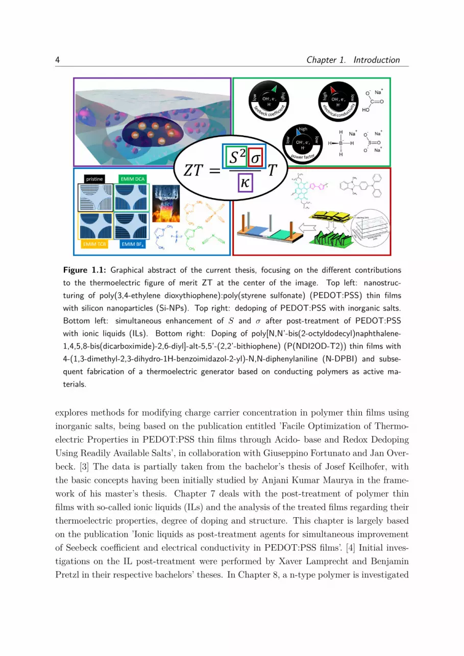
The projects in this thesis all evolve around the thermoelectric figure of merit ZT , shownin the center of Figure 1.1. Each individual project aims at the directed modification ofcertain parameters which affect the thermoelectric capabilities of conducting polymers,in order to shed light on the underlying concepts and improve the understanding of thelink between thermoelectric properties and the morphology of conducting polymer thinfilms. The main question to be answered in Chapter 5 is, whether nanostructuring ofpolymer thin films leads to a favorable decrease of the thermal conductivity or not, andwhether there is a link between the structure and thermoelectric properties. It is largelybased on the publication entitled ” ’Morphology-Function Relationship of ThermoelectricNanocomposite Films from PEDOT:PSS with Silicon Nanoparticles’, which was writtenin collaboration with Mihael Coric, Anton Greppmair and Mika Pfluger. [2] Chapter 6
4 Chapter 1. Introduction
Figure 1.1: Graphical abstract of the current thesis, focusing on the different contributionsto the thermoelectric figure of merit ZT at the center of the image. Top left: nanostruc-turing of poly(3,4-ethylene dioxythiophene):poly(styrene sulfonate) (PEDOT:PSS) thin filmswith silicon nanoparticles (Si-NPs). Top right: dedoping of PEDOT:PSS with inorganic salts.Bottom left: simultaneous enhancement of S and σ after post-treatment of PEDOT:PSSwith ionic liquids (ILs). Bottom right: Doping of poly[N,N’-bis(2-octyldodecyl)naphthalene-1,4,5,8-bis(dicarboximide)-2,6-diyl]-alt-5,5’-(2,2’-bithiophene) (P(NDI2OD-T2)) thin films with4-(1,3-dimethyl-2,3-dihydro-1H-benzoimidazol-2-yl)-N,N-diphenylaniline (N-DPBI) and subse-quent fabrication of a thermoelectric generator based on conducting polymers as active ma-terials.
explores methods for modifying charge carrier concentration in polymer thin films usinginorganic salts, being based on the publication entitled ’Facile Optimization of Thermo-electric Properties in PEDOT:PSS thin films through Acido- base and Redox DedopingUsing Readily Available Salts’, in collaboration with Giuseppino Fortunato and Jan Over-beck. [3] The data is partially taken from the bachelor’s thesis of Josef Keilhofer, withthe basic concepts having been initially studied by Anjani Kumar Maurya in the frame-work of his master’s thesis. Chapter 7 deals with the post-treatment of polymer thinfilms with so-called ionic liquids (ILs) and the analysis of the treated films regarding theirthermoelectric properties, degree of doping and structure. This chapter is largely basedon the publication ’Ionic liquids as post-treatment agents for simultaneous improvementof Seebeck coefficient and electrical conductivity in PEDOT:PSS films’. [4] Initial inves-tigations on the IL post-treatment were performed by Xaver Lamprecht and BenjaminPretzl in their respective bachelors’ theses. In Chapter 8, a n-type polymer is investigated

5
regarding the influence of electronic doping on spectroscopic, structural and thermoelec-tric properties. With the obtained knowledge from this work, a thermoelectric generatorbased on conducting polymers as active materials is fabricated. The results were obtainedwith Regina Kluge in the framework of her master’s thesis.
Finally, a brief conclusion is given in order to give answers to the questions posedthus far. An outlook into possible interesting topics shall provide stimulation for futureresearch endeavors in the field of organic thermoelectrics.


2 Theoretical background
This chapter aims at deepening the understanding of the underlying concepts for thediscussion of the results obtained in the framework of this thesis. Therefore, it is dividedinto three parts. Firstly, principles of thermoelectricity will be discussed, since theyare the foundation for understanding the obtained results in terms of power conversioncapabilities. Secondly, a theoretical foundation for conducting polymers will be layed out,since they are the primary subjects of investigation. Lastly, a section on the basics ofscattering techniques will be included. For the most part, scattering techniques aid inthe elucidation of the morphology and allow for a link to the measured thermoelectricproperties of the investigated thin films.
2.1 Thermoelectric principles
This section deals with some of the concepts involved in the description of thermoelec-tricity in general. After discussing thermoelectricity conceptually, the three main ther-moelectric effects, namely the Seebeck effect, Peltier effect and Thomson effect will bebriefly outlined. This is followed by the discussion of the thermoelectric figure of meritZT and how it can be optimized for more efficient energy conversion.
2.1.1 Thermoelectric effects
When describing thermoelectric processes, it is necessary to keep in mind that equilibriiumthermodynamics cannot be used. Upon application of a temperature gradient, the systemis forced out of thermal equilibrium. To this end, the Onsager reciprocity relations canbe used to understand forces (which represent gradients of state variables herein) andresulting fluxes in a non-equilibrium state. In thermoelectric processes, the forces comprisegradients in the temperature ∇T and the chemical potential ∇µ, which cause a flux ofparticles and heat. Correspondingly, the particle flux density J and the heat flux densityQ can be written as seen in Equations 2.1 and 2.2, respectively, in which Lij are elementsof the Onsager matrix. For further details, the reader is referred to [5].
7

8 Chapter 2. Theoretical background
− J = L111T∇µ+ L12∇
1T
(2.1)
Q = L22∇1T
+ L211T∇µ (2.2)
In simple terms, these equations describe on the one hand the direct correlation of theparticle flux density to the gradient in chemical potential ∇µ and the heat flux density tothe inverse temperature gradient ∇ 1
T, indicated by the diagonal terms Lii of the Onsager
matrix. On the other hand, the respective terms with the off-diagonal elements Lij inboth equations describe the cross-correlation. This means that e.g. the particle flux is notonly induced by the gradient in chemical potential, but also by the temperature gradient.Similarly, the heat flux is also caused by the gradient of the chemical potential.
As mentioned before, within the Onsager matrix, the diagonal matrix elements L11
and L22 represent the transport coefficients for direct correlation, while the off-diagonalelements L12 and L21 describe cross-correlations. Using the transport coefficients, impor-tant physical quantities of the thermoelectric material can be computed, according toEquations 2.3 and 2.4.
∇ 1T
= 0 ⇒ σ = e2L11
T(2.3)
J = 0 ⇒ κ = L11L22 − L12
T 2L11(2.4)
These equations show that transport of charge carriers and heat within a thermoelectricmaterial are inter-dependent and cannot be discussed separately. As will be seen lateron in this discussion, this poses several challenges with respect to the enhancement ofconversion efficiencies in thermoelectric materials.
Seebeck effect
The effect of the same name was discovered by the german physicist Thomas JohannSeebeck in the year 1821. He observed an open-circuit voltage between two dissimilarmaterials with conducting properties, when heating their junction. The conjunction oftwo materials which shows this effect is called a thermocouple. Conversely, when anelectric current flows through a junction of a thermocouple, the latter is either heated orcooled. This so-called Peltier effect, named after the french watch maker Jean Peltier, wasdiscovered in 1834. These effects are, however, related as was seen by William Thomsonin 1855, also known as Lord Kelvin. The Thomson effect states that a conductor through

2.1. Thermoelectric principles 9
which an electrical current is running and which is subjected to a temperature gradient,additionally exhibits changes in the heat flux.
However, since in the framework of this thesis, thermoelectric materials are used for thesole purpose of conversion of heat into electricity, the Seebeck effect is the most relevantfor the discussion.
When subjecting a one-dimensional conductor to a temperature gradient, both theelectric current density Je (seen in Equation 2.5) and the heat flux density JQ (seen inEquation 2.6) are influenced.
E = 1σJe + S∇T (2.5)
Q = ΠJQ − κ∇T (2.6)
Herein, σ is the electrical conductivity, S the Seebeck coefficient, Π the Peltier coef-ficient and κ the thermal conductivity. Under the influence of a temperature gradient,charge carriers within an exemplary one-dimensional solid conductor begin diffusing fromthe hot to the cold end of the gradient. This yields a surplus of charge carriers at thecold end, while leaving a deficiency of the former at the hot end. The imbalance in chargedistribution leads to an electrical potential, irrespective of the type of majority chargecarrier in the material. The magnitude of the electrical potential is proportional to themagnitude of the temperature difference and is therefore often called thermovoltage. Ad-ditionally, the thermovoltage yields a drift current, which drives charge carriers againstthe temperature gradient and is larger as more charge carriers are present. In steady-statecondition, while not canceling out, the two currents lead to a net potential which can bemeasured.
With the previous discussion, general principles for the efficiency for different typesof materials can be derived. Insulators possess theoretically high Seebeck coefficients,but very low electrical conductivities due to their inability to transport charge carriers.Metals are good electrical conductors, but typically possess low Seebeck coefficients, sincethe abundance of charge carriers leads to large drift currents. In terms of the Seebeckcoefficient, semiconductors are the material type of choice, due to their favorable com-bination of decent electrical conductivity and intermediate charge carrier concentration.For further reading on the Seebeck coefficient and thermoelectricity in general, the readeris referred to [6].
10 Chapter 2. Theoretical background
2.1.2 Thermoelectric figure of merit ZT
The thermoelectric figure of merit ZT allows for gauging the energy conversion efficiencyof a thermoelectric device, and is given in Equation 2.7.
ZT = S2σ
κT (2.7)
In this equation, S represents the Seebeck coefficient, σ the electrical conductivity,κ the thermal conductivity and T the absolute temperature. ZT is a dimensionless,temperature-dependent quantity and is directly related to the conversion efficiency η viaEquation 2.8. [7] It should be noted that in different instances, ZT can either refer to thefigure of merit of a single material or to that of a full generator. For the remainder of thisthesis, only the former is valid.
η = Th − TcTh
√1 + ZT − 1√1 + ZT + Tc
Th
(2.8)
The first part of the equation represents the Carnot efficiency and thus places an upperlimit to the electrical power which can be obtained from a certain temperature gradient,as both the hot temperature Th and the cold temperature Tc are included, as well asthe average temperature T . The second term takes the properties of the employed ther-moelectric material into account. It can be seen that the material properties, throughthe inclusion of ZT, pose an additional limitation to the energy conversion capabilities.Still, Equation 2.8 is proof that in order to efficiently convert temperature differencesinto electrical power, larger values of ZT are required. In order to achieve this, both theelectrical conductivity and the Seebeck coefficient have to be increased, while the thermalconductivity must be kept at a minimum, as seen in Equation 2.7.
Most importantly out of all the contributions to ZT, the Seebeck coefficient refers to theability of a thermoelectric material to convert temperature differences into an electricalvoltage. In a simplified approach, in which charge carriers can be considered as free, theSeebeck coefficient can be written as shown in Equation 2.9.
S = −π2
6kBe
T
TF(2.9)
In this equation, kB is the Boltzmann constant, e the elementary charge and TF rep-resents the Fermi temperature. The ratio T/TF describes the fraction of charge carrierswhich actually contribute to the charge transport, as the Pauli exclusion principle pre-vents charge carriers far from the Fermi level to be transported. TF can be computed asshown in Equation 2.10.

2.1. Thermoelectric principles 11
TF = ~2mkB
(3π2n)2/3 (2.10)
The Fermi temperature depends on the reduced Planck constant ~, the effective mass ofthe charge carriers m and the number of charge carriers n. From this, it can be concluded,that a smaller m is favorable.
In very simple terms, the electrical conductivity can be described in terms of the numberof charge carriers n, the elementary charge e and the mobility of charge carriers µ withinthe material. Their relation to the total electrical conductivity σ is shown in Equation2.11.
σ = neµ (2.11)
While a proportionality of σ to the number of charge carriers n is apparent, one also hasto take into account the latters’ respective ability to be transported within the material.This is described by the mobility µ, which in inorganic materials is calculated from thecurvature of the band structure. As is discussed below in Section 2.2.1, for polymersthe concepts are very similar. The spatial and energetic distribution of states largelydetermine the macroscopically measurable conductivity properties of a material, wherebythe former can be easily influenced in conducting polymers by enhancing the polymerstructure through secondary doping. The latter concept will be discussed in more detailin Section 2.2.1.
The thermal conductivity is a factor which negatively affects the energy conversionefficiency, as can be seen in Equation 2.7. A low thermal conductivity is favorable, as itprevents the equilibration of the temperature gradient across the material, which wouldcease all thermoelectric processes. Within a typical thermoelectric material, κ is medi-ated by contributions from both charge carriers (κch) and phonons (κph), as is shown inEquation 2.12.
κ = κch + κph = 13CelνF lel (2.12)
In a solid material, heat can be transported by phonons, i.e. vibrational modes of thelattice. However, additionally, heat is transported by the charge carriers. The chargecarrier contribution to the thermal conductivity κch can be described using the specificheat of charges Cel, their Fermi velocity νF and their mean free path lel. This contribu-tion becomes more prominent, as more charge carriers are present within the material.In inorganic thermoelectric materials, this effect leads to comparatively large thermalconductivities, which are detrimental to the conversion efficiency. On the other hand,

12 Chapter 2. Theoretical background
polymers are a suitable material class regarding the thermal conductivity due to theircomparatively low structural order. One of the problems one is faced with when at-tempting to either increase the electrical or decrease the thermal conductivity, is theirintercorrelation. As mentioned earlier, the charge carriers do not only carry electricalcharges, but also a part of the heat. Therefore, it can be concluded that the electricaland thermal conductivity cannot be fully decoupled, as is seen in the Wiedemann-Franzlaw shown in Equation 2.13.
κchσ
= LT (2.13)
The Wiedemann-Franz law states a proportionality between the electrical conductiv-ity and the charge-mediated contribution to the thermal conductivity with temperature.Therein, L is the Sommerfeld-value of the Lorenz number, with a typical value beingL = 2.44 · 10−8 WΩK−2.
2.2 Conducting polymers
The nobel prize for chemistry in the year 2000 was awarded to Hideki Shirakawa, AlanHeeger and Alan MacDiarmid for the discovery of electrical properties in doped poly-acetylene (PA). They found that treatment of PA through oxidation with agents such asiodine, bromine or chlorine leads to unprecedented electrical conductivities, approachingvalues typically found for metals. While PA has issues regarding its practicability due toits instability in ambient atmosphere, it has sparked great interest in further developmentof organic, conjugated polymers. Conjugated polymers are defined as possessing an alter-nation of single and double bounds between carbon atoms, leading to sp2-hybridization.Apart from a strictly defined geometry around the carbon atoms, the sp2-hybridizationleads to the formation of π-orbitals perpendicular to the polymer backbone with one elec-tron per carbon atom. Within this delocalized electron cloud charges are allowed to movefreely. This is dependent on the dimensional extent of the delocalization, the conformationof the monomers within the polymer backbone, etc.
Still, similarly to metals or semiconductors, the formation of π-orbitals results in aband structure of the conjugated polymer. Therefore in the following, a model will be de-scribed which allows for the understanding of the semiconducting properties of conjugatedpolymers and the description of band structures therein.
The Peierl’s instability theorem, which is schematically depicted in Figure 2.1 assumesa one-dimensional chain composed of metal atoms. In first instance, these lattice pointsare located at a constant distance a from each other. If each of these lattice points

2.2. Conducting polymers 13
Figure 2.1: Scheme of the Peierl’s instability theorem. a) One-dimensional chain of metal atomswith constant spacing a. The bands are half-filled up to the Fermi level Ef . b) Stabilization ofsystem through distortion of lattice spacing by δ, and subsequent formation of a band-gap Eg.The unit cell of the chain doubles in size, while the corresponding Brillouin zone is halved.
contributes a single electron, this leads to a half-filled band, with the Fermi level Ef
found at the maximum energy where states are occupied. This changes, however, whenconsidering a conjugated polymer such as e.g. PA. Even though each atom contributesone additional electron to the system, in this more realistic case, the alternation betweensingle and double bonds leads to changes in the lattice spacing. This is depicted inFigure 2.1b. Single and double bonds exhibit different distances between neighboringatoms, represented by δ in the scheme. This effectively doubles the size of the unit cell.Additionally, it leads to stronger interaction for the atoms with smaller nearest-neighbordistances, while the interaction becomes weaker for larger nearest-neighbor distances. Thedegenerate energy levels found in the first case, are therefore no longer present and in totallower the energy of the system by Ef − Egap/2. This can also be seen from the Brillouinzone which halves in size, and now shows the borders at k = ±π/2a. Effectively, thesystem reduces its total energy through the change in unit cell size and introduction ofthe band gap. In summary, the presence of alternating single and double bonds leadsto the formation of a band gap, with a highest-occupied molecular orbital (HOMO) anda lowest-unoccupied molecular orbital (LUMO). The magnitude of this band-gap largely

14 Chapter 2. Theoretical background
depends on parameters such as the degree of polymerization, the structure e.g. withina thin film, the degree of doping, all of which will be discussed in the following, and istypically found to be larger than for inorganic compounds.
2.2.1 Doping of conjugated polymers
This section deals with the concept of doping of conjugated polymers, strongly influencingthe obtainable electrical properties. A clear distinction will be made between the conceptsof primary doping and secondary doping, respectively.
Primary doping in conjugated polymers
Primary doping refers to the introduction or removal of charge carriers in a conjugatedpolymer through chemical oxidation or reduction processes. Depending on the polymer,either positive or negative charge carriers can then be transported. This largely dependson the energy landscape of the system in question. P-type doping is favored in systems,in which the polymer can easily transfer electrons to the dopant, i.e. a high highestoccupied molecular orbital (HOMO) level, while for n-type doping a low lowest unoccupiedmolecular orbital (LUMO) level of the polymer is required, in order to accept electronsfrom the dopant. It turns out that a favorable energy landscape is linked to the molecularstructure of the polymer, as e.g. polythiophene derivatives show mostly p-type behavior,while napthalene-diimide-based polymers show mostly n-type behavior. [8]
In the following three distinct types of charge carriers will be discussed, namely solitons,polarons and bipolarons. It shall be noted here that charge carriers in conjugated polymerscannot be described as free electrons or holes, but have to be described as quasiparticles.
Three types of the latter are shown in Figure 2.2. The formation of a neutral soliton(denoted as S0) is easily understood when inspecting the structure of the exemplarytrans-PA more closely. In trans-PA the single and double bonds can be arranged in twodifferent ways, rendering both grounds states degenerate. This means that no additionalenergy is required for the transformation of one into the other. Since both structures cancoexist on a single chain, a defect is created at the site at which they meet. This defect,which is shown as an unpaired electron in the scheme, is commonly known as a neutralsoliton. [9] This originates from the fact that the unpaired electron interacts with thechain and entails a distortion in the latter’s bond geometry. The unpaired electron andthe distortion cannot diffuse independently, which is why the soliton has to be deemeda quasiparticle. It should also be noted that the soliton itself has a spatial extent, andis thus to a certain extent delocalized over the conjugated π-system. [10] The net chargeof the chain is still zero. The latter can, however, be transformed into a positive soliton

2.2. Conducting polymers 15
(S+) through chemical oxidation or a negative soliton (S−) through chemical reduction.While the neutral soliton does not carry a charge but a spin, the opposite is true for boththe positive and negative cases. Notably, the soliton only exists in polymers in whichthere are two degenerate ground states. This is only fulfilled for trans-PA, due to its highsymmetry. Therefore, in more complex conjugated polymers solitons are typically notfound.
Depending on the number of solitons on a single PA chain, it is possible for the formerto interact with each other. If a neutral soliton interacts with a charged one, a polaron iscreated. Depending on the sign of the charged soliton, the polaron can either be positive(P+) or negative (P−), As opposed to the soliton, a polaron carries both a charge and aspin.
The third class of charge carriers is represented by the bipolarons. These can eitherbe created through the interaction of two solitons of the same charge, or through theinteraction of a polaron with a soliton of the same charge. The positive (B+) and negative(B−) bipolarons, carry double the respective charge but no spin.
Since the charge carrier concentration has a strong impact on the Seebeck coefficient,it is necessary to correlate this quantity with the preceding discussion. A high density ofcharge carriers is equivalent to an increased probability for interaction among them. Thus,
Figure 2.2: Schematic representation of three different types of charge carriers, exemplarilyshown for PA. Solitons are shown in red, polarons in green and bipolarons in blue. While asoliton can exist in a neutral, positive or negative state, polarons and bipolarons are alwayseither positively or negatively charged. The band diagrams for the different charge carrier typesare shown at the top, with filled states being indicated by black arrows.

16 Chapter 2. Theoretical background
a high charge carrier concentration is typically associated with an increased amount ofbipolarons. The more the charge carrier concentration is reduced, the more the bipolaronconcentration decreases and the polaron concentration increases. [11] This knowledgewill be used later on for the discussion of the spectroscopic characterization and thecorresponding Seebeck coefficients in Chapters 6, 7 and 8.
Secondary doping
Secondary doping refers to changes in the charge transport capabilities of a film dependingon its structure. Charges are not only transported along single polymer chains, but alsoamong multiple polymer chains. Theoretically, charge transport is best described by theSu-Schrieffer-Heeger model (SSH), shown in Equation 2.14. [10]
HSSH = H0 +Htrans +He−ph +Hstat +Hdyn (2.14)
The model includes a Hamiltonian HSSH comprised of several contributions. A one-dimensional chain comprised of carbon atoms is assumed, in which the electrons aretreated in a tight-binding approximation. Structural relaxation can be calculated betweenthe polymer and the electrons contained in the p-orbitals, while no electron-electroninteractions are present.H0 represents the total energy of the system, including electronic and phononic exci-
tations. The transfer hamiltonian Htrans describes the transfer of charges due to orbitaloverlap. With He−ph, electron-phonon scattering is implemented, which has implicationsfor band-like and hopping charge transport. Hstat and Hdyn represent static and dynamicdisorder within the polymer, respectively. Disorder influences charge transport throughphonon-assisted hopping.
For all intents and purposes, charge transport can be divided into two categories.Firstly, hopping transport is mostly found in systems of low structural order, i.e. witha large fraction of amorphous regions. It is characterized by a proportionality to tem-perature. This can be easily understood when considering a broad energy distributionof sites which can be accessed by charges. The comparatively large energy differencesrequire thermal activation for hopping transport to occur. Hopping transport is assistedby phonons, whose contribution increases with temperature. If an insufficient amount ofenergy is present, charges become trapped in low-energy states, which presents itself aslow charge mobility.

2.2. Conducting polymers 17
On the other hand, band-like charge transport is characterized by comparatively smallenergetic differences between sites, and therefore a higher mobility of charges. This isfound in polymers in which the overlap of π-orbitals between different chains is large.In these cases, one typically finds an increase of the resistance with temperature due toincreased scattering with phonons.
In general, the ability of a polymeric system to transport charges can conceptuallybe written combining the influence of primary and secondary doping, as seen in Equa-tion 2.15.
~j = σ ~E = neµ~E (2.15)
Herein, the current density ~j is described by an electric field ~E and the proportionalityconstant σ, also termed electrical conductivity. The latter, in turn, can be described interms of the number of charge carriers, and therefore by the degree of primary doping,the number of charges on a single charge carrier e, and the mobility µ which depends onthe degree of structural order/disorder and thus on the secondary doping.
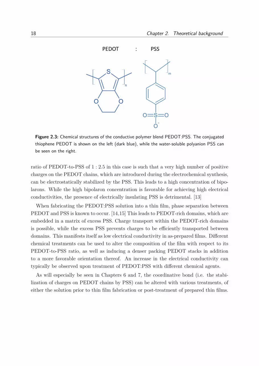
2.2.2 PEDOT:PSS
PEDOT:PSS is a water-soluble, conductive polymer blend shown in Figure 2.3. Therein,PEDOT as polythiophene allows for the transport of charges due to its conjugated back-bone. PSS stabilizes the positive charges on the PEDOT chains and renders the blendas a whole soluble in water. PEDOT is electrochemically synthesized in presence of PSS,yielding core-shell- like nanoparticles in the dispersion. These are characterized by a PSS-rich shell and a core in which short fragments are grafted onto PSS chains via coordinativebonds. [12]
PEDOT:PSS is commercially available in aqueous dispersions, which mostly differ intheir PEDOT-to-PSS ratio. This impacts properties such as the work function, trans-parency properties, viscosity, electrical properties, etc. While the different propertiesrender PEDOT:PSS suitable as transparent electrode, e.g. in organic solar cells or light-emitting diodes due to its favorable transparency properties and work function, the focusin the framework of this thesis lies on the electrical conductivity which can be achieved inthin films. Park et al. performed a systematic study, in which they varied the PEDOT-to-PSS ratio during synthesis. [13] They characterized the thin films regarding their electricalconductivities and Seebeck coefficients. A ratio of 1 : 2.5 between PEDOT-to-PSS wasfound to show the highest electrical conductivities, whereby a drastic drop was seen forhigher relative amounts of PSS. This can be easily understood when considering the in-ability of PSS to transport charge carriers, due to its lack of a conjugated π-system. The
18 Chapter 2. Theoretical background
Figure 2.3: Chemical structures of the conductive polymer blend PEDOT:PSS. The conjugatedthiophene PEDOT is shown on the left (dark blue), while the water-soluble polyanion PSS canbe seen on the right.
ratio of PEDOT-to-PSS of 1 : 2.5 in this case is such that a very high number of positivecharges on the PEDOT chains, which are introduced during the electrochemical synthesis,can be electrostatically stabilized by the PSS. This leads to a high concentration of bipo-larons. While the high bipolaron concentration is favorable for achieving high electricalconductivities, the presence of electrically insulating PSS is detrimental. [13]
When fabricating the PEDOT:PSS solution into a thin film, phase separation betweenPEDOT and PSS is known to occur. [14,15] This leads to PEDOT-rich domains, which areembedded in a matrix of excess PSS. Charge transport within the PEDOT-rich domainsis possible, while the excess PSS prevents charges to be efficiently transported betweendomains. This manifests itself as low electrical conductivity in as-prepared films. Differentchemical treatments can be used to alter the composition of the film with respect to itsPEDOT-to-PSS ratio, as well as inducing a denser packing PEDOT stacks in additionto a more favorable orientation thereof. An increase in the electrical conductivity cantypically be observed upon treatment of PEDOT:PSS with different chemical agents.
As will especially be seen in Chapters 6 and 7, the coordinative bond (i.e. the stabi-lization of charges on PEDOT chains by PSS) can be altered with various treatments, ofeither the solution prior to thin film fabrication or post-treatment of prepared thin films.
2.2. Conducting polymers 19
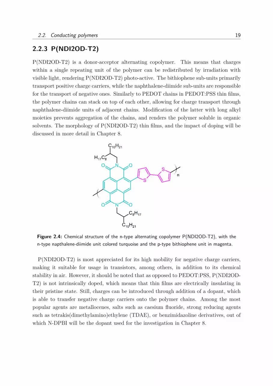
2.2.3 P(NDI2OD-T2)
P(NDI2OD-T2) is a donor-acceptor alternating copolymer. This means that chargeswithin a single repeating unit of the polymer can be redistributed by irradiation withvisible light, rendering P(NDI2OD-T2) photo-active. The bithiophene sub-units primarilytransport positive charge carriers, while the naphthalene-diimide sub-units are responsiblefor the transport of negative ones. Similarly to PEDOT chains in PEDOT:PSS thin films,the polymer chains can stack on top of each other, allowing for charge transport throughnaphthalene-diimide units of adjacent chains. Modification of the latter with long alkylmoieties prevents aggregation of the chains, and renders the polymer soluble in organicsolvents. The morphology of P(NDI2OD-T2) thin films, and the impact of doping will bediscussed in more detail in Chapter 8.
Figure 2.4: Chemical structure of the n-type alternating copolymer P(NDI2OD-T2), with then-type napthalene-diimide unit colored turquoise and the p-type bithiophene unit in magenta.
P(NDI2OD-T2) is most appreciated for its high mobility for negative charge carriers,making it suitable for usage in transistors, among others, in addition to its chemicalstability in air. However, it should be noted that as opposed to PEDOT:PSS, P(NDI2OD-T2) is not intrinsically doped, which means that thin films are electrically insulating intheir pristine state. Still, charges can be introduced through addition of a dopant, whichis able to transfer negative charge carriers onto the polymer chains. Among the mostpopular agents are metallocenes, salts such as caesium fluoride, strong reducing agentssuch as tetrakis(dimethylamino)ethylene (TDAE), or benzimidazoline derivatives, out ofwhich N-DPBI will be the dopant used for the investigation in Chapter 8.

20 Chapter 2. Theoretical background
2.3 Scattering basics
Scattering techniques are powerful tools for structure analysis of polymeric materials. Asopposed to many real-space scanning probe techniques, they allow for structural analysisin reciprocal space. This yields statistically relevant information not only of surfaces, asis the case for many real-space techniques, but also of buried objects and interfaces. Espe-cially for thin film samples the so-called grazing-incidence geometry offers the advantageof a large illuminated sample volume, which in the case of a x-ray beam impinging per-pendicularly would be much smaller. For our purposes, the grazing-incidence geometry isused in order to elucidate the structure of organic thermoelectric thin films on differentlength scales. In the following, scattering basics shall be discussed for x-rays, whereas itshould be noted that these concepts also apply for neutrons.
The interaction of a material with x-rays can be discussed in terms of the energy(E)-dependent refractive index n, shown in Equation 2.16.
n(E) = 1− δ(E) + iβ(E) (2.16)
Herein, the real contribution δ represents the dispersion properties, while the imaginarycontribution β represents the absorption properties of a material. Notably, the refractiveindex n and its components are energy-dependent, which is of importance for the discus-sion below. Within the hard x-ray regime with typical photon energies larger than 5 keV,dispersion values lie in the range of 10−5 to 10−6, while absorption values lie in the rangeof 10−7 to 10−8. As a consequence, the refractive index for most organic materials issmaller than one in the hard x-ray regime. Thus, when traversing from an optically densemedium (e.g. air) into a polymer thin film, total reflection occurs with the x-ray beamimpinging under a sufficiently shallow angle. The angle above which the beam penetratesthe film is called the critical angle αc and can be approximated using the dispersion, asseen in Equation 2.17.
αc =√
2δ (2.17)
This approximation especially holds in the hard x-ray regime and far from resonanceenergies of atomic species contained in the sample, where absorption can be neglected. Forthe case of resonant x-ray scattering, which will be discussed below, the absorption con-tribution is non-negligible and the critical angle can be calculated according to Equation2.18.
αc = 90°−Re(arcsin(n)) (2.18)

2.3. Scattering basics 21
Nevertheless, the critical angle is an important quantity regarding the grazing-incidencescattering experiments, performed throughout this thesis. In scattering patterns collectedin the grazing-incidence geometry, as is done in the frame of this thesis, a maximum inthe diffuse scattering is found at the critical angle of the illuminated material. [16] At thisposition, a material-sensitivity of the scattering signal is achieved, as the critical angleitself is a material-dependent property. Due to the plethora of materials with varyingcompositions and constitutions, no database with measured values for δ and β for allpossible materials as function of energy exists. Thus, it is of high importance to be ableto theoretically predict the optical properties of materials. Henke et al. tabulated valuesfor atomic scattering form factors f as function of energy for all chemical elements, whichdetermine the response towards x-ray radiation. [17] Alternatively, the HEPHAESTUSsoftware package can be used for simple predictions of the atomic scattering form factors.Equation 2.19 shows the energy-dependence of the atomic scattering form factors fi, aswell as the imaginary contribution.
f = f 0i + f ′i(E) + if ′′i (E) (2.19)
With the knowledge of the chemical composition of the investigated sample, the so-called scattering length density (SLD) can be calculated according to Equation 2.20.Each type of element is included by taking into account its stoichiometric fraction ci,together with the respective total atomic scattering form factor fi. The electron densityis represented by ρe, while r0 = e2/(4πε0mec
2) is the classical Thomson scattering radiusand Zi the total number of electrons within the investigated species. The former can alsobe written in terms of the mass density ρ, the Avogadro constant NA, and the molar massMi.
SLD = r0ρe
∑Ni=1 cifi∑Ni=1 Zi
= r0ρNA
∑Ni=1 cifi∑Ni=1 Mi
(2.20)
The SLD of a material is calculated from f, which contains both real and imaginarycontributions. Therefore, the SLD can be deconstructed similarly, with the real part beingused for the calculation of the dispersion, and the imaginary for the calculation of theabsorption, as can be seen in Equations 2.21 and 2.22, respectively.
δ(E) = λ2
2πRe(SLD) (2.21)
β(E) = λ2
2πIm(SLD) (2.22)

22 Chapter 2. Theoretical background
2.3.1 Grazing-incidence scattering
Grazing-incidence scattering is a suitable method for the structure determination in thinfilms. While the path length of an incident beam in the thin film would be very smallwhen measuring in a transmission geometry in which the beam impinges the sampleperpendicularly, the grazing-incidence geometry leads to a large illuminated area. This isdue to a combination of a shallow incident angle, which typically below 1°, and small butfinite spatial dimensions of the beam itself. As a result, one obtains enhanced statisticsdue to a macroscopically probed sample volume. Additionally, through careful variationof the incident angle below or above the critical angle of the investigated material, thescattering signal predominantly originates from only the surface or the surface and bulkof the film, respectively.
The electric field of the incident beam is modified through the interaction with theilluminated material, and thus scattered. Equation 2.23 shows the general definitions andcontributions to the scattering vector ~q. Herein, α denotes angles in the scattering plane,while ψ represents out-of-plane angles. The subscripts i and f denote incident and exitangles, respectively. Equation 2.23 therefore links the reciprocal q-vectors to the real-space exit angles. Generally, elastic scattering occurs when plane electromagnetic wavesinteract with a single object with a characteristic shape and the magnitude of the vectoris unchanged.
q = 2πλ
qx
qy
qz
= 2πλ
cos(ψf )cos(αf )− cos(αi)
sin(ψf )cos(αf )sin(αi) + sin(αf )
(2.23)
Grazing-incidence small-angle scattering (GISAS)
As the name implies, in grazing-incidence small-angle scattering, only scattering in smallexit angles is captured on the detector, which can be ensured by having large sample-to-detector distances (SDDs). This has several implications, and allows for the simplificationof the scattering vector q, as seen in Equation 2.24.
q = 2πλ
0
2ψfαi + αf
(2.24)

2.3. Scattering basics 23
The components qx, qy and qz represent the scattering contribution in direction of thebeam, perpendicular to the beam but parallel to the substrate and perpendicular to bothbeam and substrate, respectively. The former contribution can be neglected, while itbecomes additionally possible to decouple scattering in horizontal and vertical direction,and therefore qy and qz.
A factor which has to be taken into account is the possibility of a single photon beingscattered multiple times. This originates from the large footprint of the beam on thesample. Due to the drastically increased path length of the beam in the sample, theprobability for multiple scattering events is greatly enhanced. The Born approximationassumes scattering of photons as consequence of the interaction with a homogeneous scat-terer. In the grazing-incidence geometry this assumption does not hold any more, whichis why the former has to be modified. The so-called distorted-wave Born approximation(DWBA) is a perturbation-theoretical treatment of the Born approximation and accountsfor the presence of a substrate layer and various combinations of reflection and refractionevents. More specifically, it differentiates between (1) simple refraction off a scatterer, (2)reflection from the substrate layer prior to refraction off a scatterer, (3) reflection fromthe substrate layer after refraction off a scatterer and (4) reflection from the substratebefore and after refraction off a scatterer. The DWBA treats the scattered intensity asresult of the superposition of photons scattered according to the four afore-mentionedprocesses. [18]
In the framework of the DWBA, the scattering cross-section can be described accordingto Equation 2.25.
dσ
dΩ |diff = Cπ2
λ4 ∆n2(E)|tFi |2|tFf |2Pdiff (~q) (2.25)
Herein, C represents the illuminated surface area, while ti and tf are the Fresnel trans-mission coefficients for the incident and exiting beam, respectively. ∆n(E)2 describesthe energy-dependent scattering contrast between e.g. a scatterer and its surroundingmedium. In the discussion of resonant x-ray scattering below in Section 2.3.2, this will beof importance. Lastly, the diffuse scattering factor Pdiff takes into account the structureof the sample on the mesoscale. [19] The form factor F(~q) refers to the average shape ofscattering objects, while the spatial distribution of the latter can be parametrized in thestructure factor S(~q). Since there is often no significant order on the mesoscale in poly-meric thin films, S(~q) typically represents a paracrystalline lattice, in which the scatterersare placed. Additionally, Pdiff is proportional to the number N of scatterers present inthe illuminated area.
Pdiff (~q) ∝ NF (~q)S(~q) (2.26)

24 Chapter 2. Theoretical background
For the analysis, several simplifications are being made which will be listed in thefollowing. As the simulation of a full 2D grazing-incidence small-angle x-ray scattering(GISAXS) pattern is computationally expensive, an alternative route for the structureanalysis is taken. Instead, line profiles from the pattern are extracted vertically or hori-zontally. While the former contain information on correlation perpendicular to the sub-strate and the chemical composition, the latter are used for modelling and elucidationof lateral structure shapes, sizes and spatial arrangements. It is allowed to treat bothcomponents as decoupled. The vertical line cuts can be used to determine the positionof the Yoneda peak of a material in question, at which point the corresponding scatter-ing contribution is maximal. [16] On the other hand, in the horizontal line cuts spatialcorrelation of structures is only considered in lateral, not in vertical direction. In otherwords, the qz-component is considered constant in the horizontal line profiles. [20] Since,however, in polymer systems one not only finds objects with a monodisperse size distri-bution, but rather a polydisperse one, the variation in sizes has to be taken into account.The relation seen in Equation 2.26 has to be modified by adding the average form factor〈F (~q)〉, as seen in Equation 2.27.
Pdiff (~q) ∝ N 〈F (~q)〉S(~q) (2.27)
Most often, modeling is done in the framework of the decoupling approximation (DA)or the local monodisperse approximation (LMA). [21] In the DA, all objects interactwith each other and collectively contribute to the scattering signal. It holds better insystems with small polydispersities, as position and type of scatterers are uncorrelated.On the other hand, in the LMA different ’families’ of objects are regarded as spatiallyseparated, thus leading to selective interaction of domains within one structural family.Scattering between objects of different families is not included in the LMA model. Forthe modelling, form factors representing spherical objects are used. As mentioned above,these are arranged in a one-dimensional para-crystalline lattice, in which the distancesbetween objects are also subject to a certain statistical variation.
It should be noted that all aforementioned concepts hold true for both x-ray and neutronscattering.
2.3.2 Grazing-incidence resonant tender x-ray scattering (GIR-TeXS)
Resonant x-ray scattering is a modified version of scattering with hard x-rays. Onereason for that is the strongly enhanced chemical sensitivity, due to measurements beingcarried out with x-ray wavelengths adjusted to core-electronic transitions of constituentchemical species. Due to the effect of chemical shift on the fine structure in atomic

2.3. Scattering basics 25
absorption spectra close to absorption edges, the components of the refractive index shownin Equation 2.16 change drastically and non-linearly.
Equations 2.21 and 2.22 have important implications for the elucidation of opticalproperties of the investigated materials, as β(E) can be determined from absorptionmeasurements in the x-ray range according to Equation 2.28.
β(E) = µρ
2k = µρhc
4πE (2.28)
In this equation, h is the Planck constant, c the speed of light and ρ the density of thematerial. Since the real part of the refractive index δ cannot be measured directly, it hasto be determined as function of energy from β using the Kramers-Kronig relations, shownin Equations 2.29 and 2.30. [22] For this purpose, the freely available software packageKKcalc is used. The calculation of integrals with infinity as boundaries which would benecessary for the determination of δ from the Kramers-Kronig relation is circumventedwith the help of the so-called Henke-database. [17] It lists photoabsorption cross-sectionsand atomic scattering factors, which relate to β and δ, respectively, for each single elementin a range from 50 eV to 30 000 eV. For the energies outside the range of the near-edgex-ray absorption fine structure (NEXAFS) spectra, the KKcalc software plugs in thedatabase values, thus allowing for the calculation of the quasi-infinite integral.
δ(E) = 2π℘
∫ ∞0
E ′β(E ′)E ′2 − E2dE
′ (2.29)
β(E) = −2E ′π℘
∫ ∞0
δ(E ′)E ′2 − E2dE
′ (2.30)
Using the Kramers-Kronig relations it becomes possible to determine the dispersionproperties in the vicinity of absorption edges with the knowledge of their correspondingabsorption properties. This allows for the calculation of the energy-dependent scatteringcontrast ∆n2(E), which is shown in Equation 2.31.
∆n2(E) = ∆δ2(E) + ∆β2(E) = (δ1(E)− δ2(E))2 + (β1(E)− β2(E))2 (2.31)
∆n2(E) can only be calculated for a pair of two materials, for one of which the opticalproperties are denoted with index 1, while for the other the index 2 is used. Referringback to the scattering cross-section in a GISAXS experiment shown in Equation 2.25,its dependency on the diffuse scattering factor Pdiff , the Fresnel transmission coefficientsand the scattering contrast ∆n2 is apparent. This has implications for the analysis ofthe 2D grazing-incidence resonant tender x-ray scattering (GIR-TeXS) data, as will bediscussed in Section 3.3.3.

26 Chapter 2. Theoretical background
Grazing-incidence wide-angle scattering (GIWAXS)
As opposed to GISAXS, in a grazing-incidence wide-angle x-ray scattering (GIWAXS)experiment scattering under large angles is captured on a 2D detector. Translating fromlarge q-values in reciprocal space, one obtains information on possible structural order onshort length scales in the investigated material. As opposed to a x-ray diffraction (XRD)measurement, additionally possible preferred orientation of structural elements within thematerial can be discerned.
Ewald’s construction aids in the understanding of the processes which lead to distinctscattering peaks in the final image. In contrast to the theoretical description of thescattering vector ~q in GISAXS, the small-angle approximation does not hold anymore, asthe curvature of the Ewald’s sphere is no longer negligible. This leads to the descriptionof the scattering vector according to Equation 2.23.
Generally speaking, the occurrence of a scattering signal relies on the intersection of thesurface of the Ewald’s sphere with the reciprocal lattice of the material. The size of theformer directly correlates to the employed wavelength of the x-ray beam. This necessitatesthe fulfillment of the so-called Laue condition, which states that the scattering vector~q = ~G. Geometrically speaking, the scattering vector ~G represents any reciprocal latticepoint that intersects with the Ewald’s sphere, and thus yields a signal on the detector.In turn, this leads to the condition of elastic scattering, such that the magnitude of theincident wave vector ~ki is equal to that of the exiting wave vector ~kf .
Collection of large scattering angles in a GIWAXS experiment has ramifications onthe correct representation of data and the information which can be obtained. Mostimportantly, when converting the data into reciprocal space, the information on verticalcorrelation within the film, thus in qz-direction, is not accessible in a GIWAXS mea-surement. This so-called ’missing wedge’ appears due to the significant curvature of theEwald’s sphere, and a strong requirement for contributions of the other reciprocal latticevectors ~qx and ~qy. In reciprocal space a scattering vector ~q with a certain magnitudewhich can be oriented in all possible directions, spans a so-called orientation sphere. Theintersection of the latter with the Ewald’s sphere will determine if a scattering peak willappear on the detector or not. In other words, a diffraction peak with a certain magnitudeof its q-vector in z-direction has to be tilted in either qx- or qy-direction, in order to beprojectable on the Ewald’s sphere and ultimately show the scattering signal. Accordingly,at larger qz-values the missing wedge becomes larger with respect to the polar angle χ. [23]This so-called χ-correction, among others, is discussed in more detail in Section 3.3.3.
3 Characterization methods
Different methods used for the characterization of thermoelectric thin films are discussedin this chapter. The first section deals with the thermoelectric characterization, includingmeasurement methods for the Seebeck coefficient, the electrical and thermal conductivity.Afterwards, spectroscopic techniques are discussed which are used for deeper understand-ing of the electronic structure, composition and conformational states in polymer films.Lastly, characterization techniques for the analysis of thin film structures using electronmicroscopy and scattering techniques with a special focus on GIWAXS and GIR-TeXSare described.
3.1 Thermoelectric characterization
The measurement of thermoelectric properties in conducting polymer thin films representsthe main focus of this thesis, as it allows for gauging of the feasibility of certain treatmentsregarding power conversion efficiency and for linking the observations to properties of thethin films, such as the composition, structure, etc. This section deals with the experimen-tal setups used for measurement of the Seebeck coefficient, the electrical conductivity, thefilm thickness and the thermal conductivity of conducting polymer films.
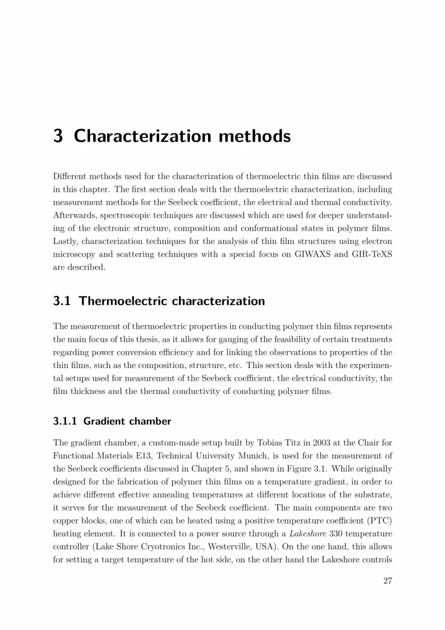
3.1.1 Gradient chamber
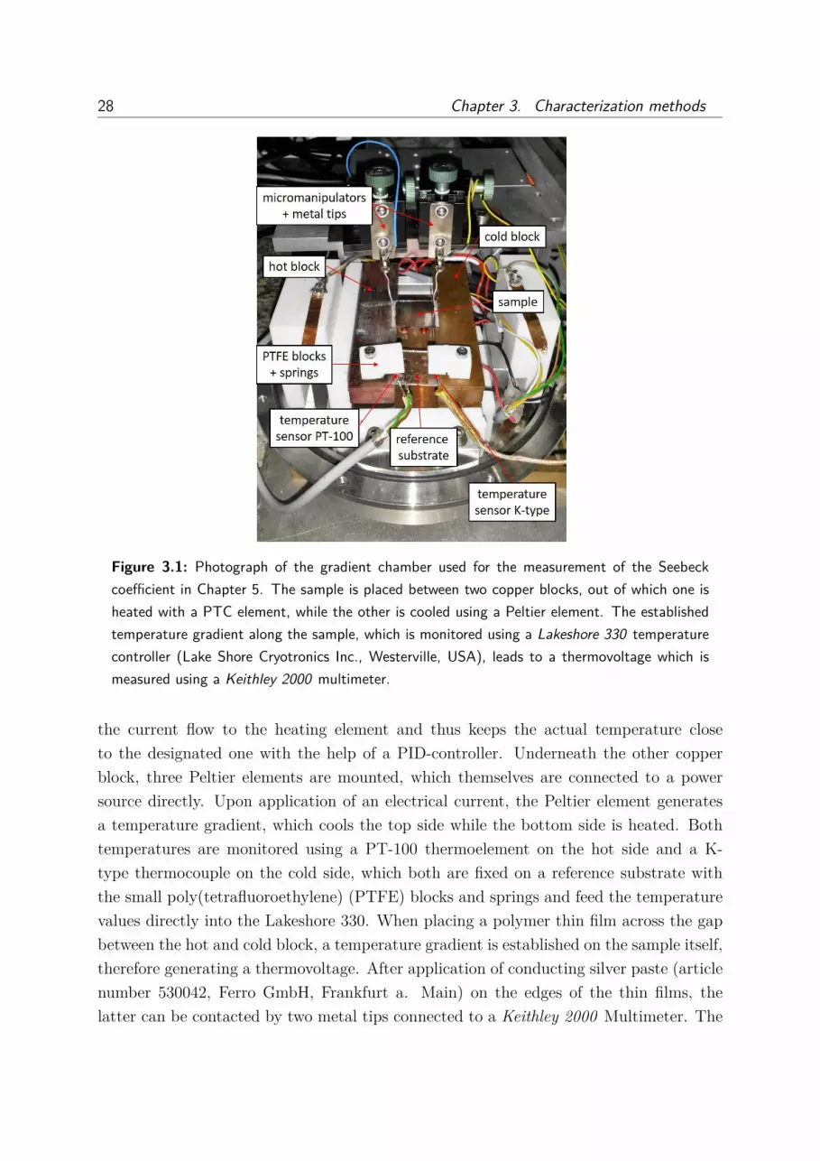
The gradient chamber, a custom-made setup built by Tobias Titz in 2003 at the Chair forFunctional Materials E13, Technical University Munich, is used for the measurement ofthe Seebeck coefficients discussed in Chapter 5, and shown in Figure 3.1. While originallydesigned for the fabrication of polymer thin films on a temperature gradient, in order toachieve different effective annealing temperatures at different locations of the substrate,it serves for the measurement of the Seebeck coefficient. The main components are twocopper blocks, one of which can be heated using a positive temperature coefficient (PTC)heating element. It is connected to a power source through a Lakeshore 330 temperaturecontroller (Lake Shore Cryotronics Inc., Westerville, USA). On the one hand, this allowsfor setting a target temperature of the hot side, on the other hand the Lakeshore controls
27
28 Chapter 3. Characterization methods
Figure 3.1: Photograph of the gradient chamber used for the measurement of the Seebeckcoefficient in Chapter 5. The sample is placed between two copper blocks, out of which one isheated with a PTC element, while the other is cooled using a Peltier element. The establishedtemperature gradient along the sample, which is monitored using a Lakeshore 330 temperaturecontroller (Lake Shore Cryotronics Inc., Westerville, USA), leads to a thermovoltage which ismeasured using a Keithley 2000 multimeter.
the current flow to the heating element and thus keeps the actual temperature closeto the designated one with the help of a PID-controller. Underneath the other copperblock, three Peltier elements are mounted, which themselves are connected to a powersource directly. Upon application of an electrical current, the Peltier element generatesa temperature gradient, which cools the top side while the bottom side is heated. Bothtemperatures are monitored using a PT-100 thermoelement on the hot side and a K-type thermocouple on the cold side, which both are fixed on a reference substrate withthe small poly(tetrafluoroethylene) (PTFE) blocks and springs and feed the temperaturevalues directly into the Lakeshore 330. When placing a polymer thin film across the gapbetween the hot and cold block, a temperature gradient is established on the sample itself,therefore generating a thermovoltage. After application of conducting silver paste (articlenumber 530042, Ferro GmbH, Frankfurt a. Main) on the edges of the thin films, thelatter can be contacted by two metal tips connected to a Keithley 2000 Multimeter. The

3.1. Thermoelectric characterization 29
thermovoltage measured on the multimeter is then divided by the temperature gradientfrom the hot to the cold side in order to obtain the Seebeck coefficient, using Equation3.1.
S = ∆V(Th − Tc)
(3.1)
Here, ∆V is the measured thermovoltage, while Th and Tc represent the temperatureson the hot and cold side in Kelvin, respectively. The temperature of the hot side was setto 100 C, while the cold side equilibrated at 15 C. A stable temperature gradient of 85 Kwas established. An average value for the Seebeck coefficient is obtained by repeating themeasurement multiple times.
It should be noted that the gradient chamber turned out to show severe problems. Theseinclude a lack of reproducible contact pressure of the metal tips for the thermovoltagemeasurement and measurement of the temperatures on a reference substrate instead ofthe sample itself. In addition, the setup cannot be operated under vacuum by sealingthe chamber with the corresponding lid, since the heat generation from both the PTCand Peltier element cannot be dissipated into the environment, but is instead stored inthe metal encasing, which is thermally in contact. This may lead to overheating of thecomponents, and their subsequent failure. The gradient chamber also lacks a reliableway of mounting it at beamlines in synchrotrons for performing in-situ/in-operando x-rayscattering measurements. All of these issues are tackled with the conceptualization andimplementation of the x-ray analysis voltage-emulation rig (XAVER), discussed in thefollowing section.
3.1.2 XAVER: X-ray analysis voltage-emulation rig
XAVER was built by Xaver Lamprecht (bachelor’s thesis 2016, Chair for Functional Ma-terials E13, Technical University Munich) in the frame of this thesis, and aims at solvingsome of the issues which one faces during operation of the gradient chamber. It is used formeasuring Seebeck coefficients in Chapters 6, 7 and 8, and also temperature-dependentresistances for the latter.
In general, it can be said that the XAVER is designed for the measurement of ther-moelectric properties of thin films, especially the Seebeck coefficient and temperature-dependent resistance. To this end, XAVER can be used in two different configurations,namely the Seebeck configuration, shown in Figure 3.2 and the two-point configurationin Figure 3.3.

30 Chapter 3. Characterization methods
Figure 3.2: Exploded view of the Seebeck configuration of XAVER. Numbered elements corre-spond to: 1) ’Hot’ copper block with heating cartridge, 2) Peltier element with copper blockfor the attachment of an external cooling circuit (gray) underneath, and thin copper plate formatching the height of the ’hot’ copper block, 3) copper plate with extended slots for distanceadjustment of the ’hot’ and ’cold’ block, 4) PTFE spacer for thermal disconnection of the hotcopper block from the copper plate, 5) PTFE bridges containing copper tips and Pt-100 temper-ature sensors for measurement of the thermovoltage and temperature, respectively, 6) aluminumbase plate and 7) PTFE feet for fixing the measurement setup on the base plate. [24]
The design of XAVER differs in many aspects from the gradient chamber. The heatingcartridge (100 W, 6 mm · 33 mm two-pole version, Friedrich Freek GmbH) inside the cop-per block (copper alloy W-200, Albromet GmbH) on the hot side (designated as number 1)and the Peltier element (70 W, 42147/UEPT-130-071-120M150S, uwe electronic GmbH,designated as number 2) are responsible for heating and cooling, respectively. Both the’hot’ and ’cold’ copper block rest on top of a copper plate (copper alloy W-200, AlbrometGmbH, designated as number 3), whose two slots along the length of the plate allow foradjustment of the distance between the hot and cold copper blocks. Thus, even sam-ples with differing sizes or electrode distances can be accomodated and measured. Thehot copper block is thermally disconnected from the copper plate using a PTFE spacer(number 4). Dissipation of the heat generated upon operation of the Peltier element ispossible through the inclusion of the copper block underneath (shown in grey), whichhas two attaching points. An external cooling circuit can be plugged into the block, act-

3.1. Thermoelectric characterization 31
Figure 3.3: Two-point configuration of XAVER. The ’hot’ copper block with the heating car-tridge is thermally connected to the copper plate, allowing for homogeneous heating of thesample. In order to measure temperature-dependent resistances, a constant electrical bias volt-age is applied, while simultaneously measuring the current and the temperature. The PTFE feeton both sides of the copper plates thermally disconnect the setup from the base plate, and bringthe sample into the pivot point of the chamber. [24]
ing as heat sink and therefore allowing for transfer of the heat to the cooling medium,thus allowing the Peltier element to run properly even in an evacuated environment.The measurement of both thermovoltage and temperature on both ends of the sampleis done using the PTFE bridges (number 5). These contain copper tips for the thermo-voltage measurement and rod-like Pt-100 temperature sensors (Pt-100, class A, 4-wireconfiguration, encased, −50 C to 200 C, Thermo Sensor GmbH). Since the temperatureis measured directly on the sample, and both the copper tips and temperature sensorsare pressed on the sample with springs (spring constant 1 N), the measurement is morereproducible. The signals of the thermovoltage and temperature measurement are bothfed through a 16-pole, vacuum-tight wall conducting plug system (SGJ.1B.316.CLLSV,FGG.1B.316.CLAD76, FGJ.1B.316.CLLD76, Lemo Electronic GmbH) to the Keithley2000 multimeter and Lakeshore 330 temperature controller, respectively. This allows forencasing of the setup in the vacuum chamber discussed below. The whole setup rests ontop of a base plate (number 6), but is thermally disconnected from the latter through thePTFE feet (number 7).
The two-point configuration shown in Figure 3.3 allows for the study of charge transport

32 Chapter 3. Characterization methods
properties of polymer thin films. For this purpose, the components of the XAVER arere-arranged in a way that the heating cartridge heats the copper plate homogeneously.When placing the sample on the copper plate it is also heated homogeneously. Thus,when applying a bias voltage U using a Keithley 2400 sourcemeter, and measuring thecurrent I, a dependency of the resistance as function of temperature can be inferred. Theresistance is calculated according to Equation 8.1.
R = U
I(3.2)
This is especially useful for the discussion of the results in Chapter 8, since the resis-tances of P(NDI2OD-T2) films are typically very high. Therein, electrical conductivitiesare calculated in in-plane and cross-plane direction, taking into account the resistancevalues from Equation 8.1 and the film thickness t, the distance d and length l of theelectrodes and the overlap area A of the electrodes, as seen in Equations 3.3 and 3.4,respectively.
σin = d
Rtl(3.3)
σout = t
RA(3.4)
Figure 3.4: Photograph of the addition to XAVER made for easier contactability of samples withirregular geometries/dimensions used for measurement of temperature-dependent resistances ofP(NDI2OD-T2) films (left) and for measurement of thermoelectric generators (right) discussedin Chapter 8. [25]

3.1. Thermoelectric characterization 33
An addition to the XAVER was made, in order to facilitate the measurement of the high-resistance P(NDI2OD-T2) films, discussed in Chapter 8. The additional set of copper-beryllium tips is shown in Figure 3.4. Due to the varying geometries in which P(NDI2OD-T2) thin films are prepared, the ability to accurately position the measurement tips on theelectrodes, and having the former also connected to a Keithley 2400 sourcemeter, allowedfor the measurement of temperature-dependent resistances. In general, measurementof the resistance as function of temperature is a facile way of getting insight into thecharge-transport properties of polymer thin films. Samples in which hopping transport isprevalent, show a decrease of the resistance with increasing temperature. For samples inwhich band-like transport is dominant, the opposite is the case.
Measurement of the electric parameters of the thermoelectric generators discussed inChapter 8 became possible using this device, by using it to contact one of the fluorine-doped tin oxide (FTO) electrodes on the edge of the substrate. The PTFE bridgeswere used to measure the temperature on top of the center aluminum electrode (the’cold’ end of the generator) and contact the other FTO electrode while measuring itstemperature (the ’hot’ end of the generator), respectively. Thermovoltages were measuredby applying a temperature gradient between 5 C to 10 C perpendicular to the substrate,and monitoring the output voltage U by contacting the FTO electrodes on either end ofthe substrate. The power output P was determined according to Equation 3.5.
P = U2
R(3.5)
In order to measure the resistance R of the device, different bias voltages were appliedwhile the induced current was measured over time. According to Ohm’s law (Equation8.1), the resistance can be calculated using the slope obtained from a linear fit in the U-Iplot.
Another feature of the XAVER is the vacuum chamber, which makes the implemen-tation at synchrotron beamlines possible. Both the chamber and the adapter plate areshown in Figure 3.5. The chamber is fabricated from a large block of aluminum. It pos-sesses both in- and outlets for the x-ray beam, which are elongated along the width of thechamber, making it possible to arrange the hot and cold copper blocks in a way that dif-ferent sample geometries can be accomodated. The Kapton windows (300 HN, polyimidederivative, Du Pont de Nemours, Luxembourg) on the in- and outlet for the x-ray beamallow for scattering experiments in the chamber due to their high x-ray transmissivitywhile also ensuring vacuum-tightness of the chamber. The height of both configurationsof the measurement setup inside the chamber is chosen in a way that the sample rests onthe pivot point, facilitating x-ray scattering measurements. Additionally, two tubes canbe attached to the side of the chamber in order to lead the external cooling circuit out.
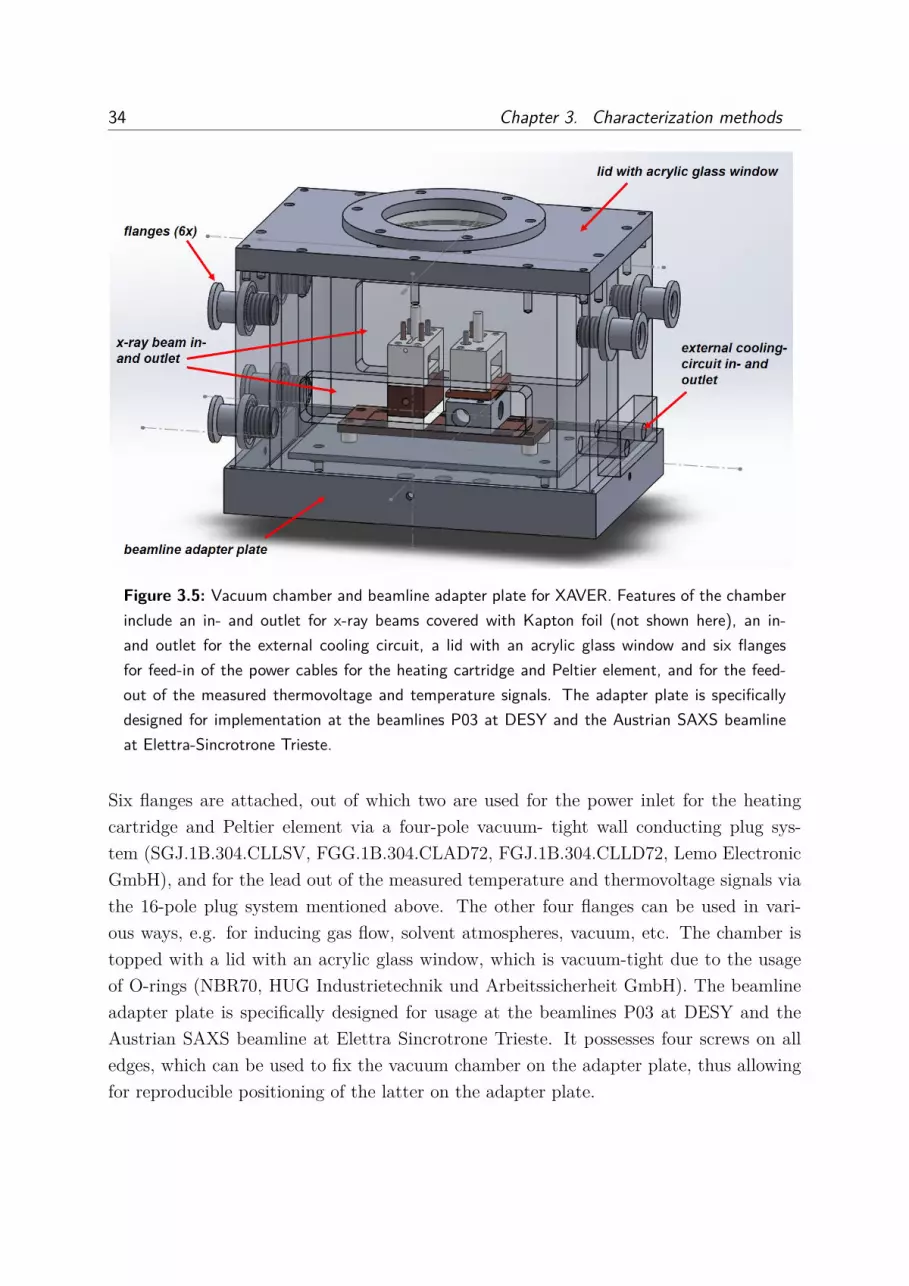
34 Chapter 3. Characterization methods
Figure 3.5: Vacuum chamber and beamline adapter plate for XAVER. Features of the chamberinclude an in- and outlet for x-ray beams covered with Kapton foil (not shown here), an in-and outlet for the external cooling circuit, a lid with an acrylic glass window and six flangesfor feed-in of the power cables for the heating cartridge and Peltier element, and for the feed-out of the measured thermovoltage and temperature signals. The adapter plate is specificallydesigned for implementation at the beamlines P03 at DESY and the Austrian SAXS beamlineat Elettra-Sincrotrone Trieste.
Six flanges are attached, out of which two are used for the power inlet for the heatingcartridge and Peltier element via a four-pole vacuum- tight wall conducting plug sys-tem (SGJ.1B.304.CLLSV, FGG.1B.304.CLAD72, FGJ.1B.304.CLLD72, Lemo ElectronicGmbH), and for the lead out of the measured temperature and thermovoltage signals viathe 16-pole plug system mentioned above. The other four flanges can be used in vari-ous ways, e.g. for inducing gas flow, solvent atmospheres, vacuum, etc. The chamber istopped with a lid with an acrylic glass window, which is vacuum-tight due to the usageof O-rings (NBR70, HUG Industrietechnik und Arbeitssicherheit GmbH). The beamlineadapter plate is specifically designed for usage at the beamlines P03 at DESY and theAustrian SAXS beamline at Elettra Sincrotrone Trieste. It possesses four screws on alledges, which can be used to fix the vacuum chamber on the adapter plate, thus allowingfor reproducible positioning of the latter on the adapter plate.

3.1. Thermoelectric characterization 35
3.1.3 4-point probe measurement
Four-point probe measurements for the determination of sheet resistances in PEDOT:PSSthin films are carried out with a Cascade Microtech (C4S-54/5) setup. Therein, fourequidistant tungsten carbide tips with a spacing of 1 mm, tip radii of 125µm are placedon the thin film, as can be seen in Figure 3.6. Since the tips are mounted on a spring,piercing of the films is prevented. A current I is applied on the outer two tips, while theinner two tips measure the induced voltage U.
The four-point probe setup allows for the measurement of sheet resistances, while ex-cluding contact resistances from the tips and wires. The sheet resistance can be calculatedusing Equation 3.6, and then be used in conjunction with the film thickness d, to calculatethe electrical conductivity in S/cm, according to Equation 3.7.
Rsh = π
ln2U
I(3.6)
σ = 1Rshd
(3.7)
It should be noted that above equations especially hold when the film thickness d ismuch smaller than the characteristic distance of the tips, as is the case throughout thisthesis. Values for the sheet resistance are typically given in Ohms per square (Ω/sq),representing the resistance of 1 Ω along the direction of a square sheet of any size.
Four-point probe measurements are carried out on up to seven positions on the sample,with the thicknesses measured at the corresponding positions using surface profilometry,discussed below. The electrical conductivity was calculated for each position, and thenaveraged over the whole sample.
Figure 3.6: Scheme of the four-point probe measurement setup, with the outer two tips usedfor current application, while the inner two are used for measurement of the resulting voltage.

36 Chapter 3. Characterization methods
3.1.4 Surface profilometry
Surface profilometry is a facile way of determining thicknesses of thin polymer thin films.In the framework of this thesis, a DekTak XT surface profiler by Bruker Corporation,Billerica, USA is used. The obtained thickness values are primarily used for calculationof the electrical and thermal conductivity and for absorption coefficients in UV-Vis andNEXAFS spectra.
Measurements are carried out by introducing scratches into the films with metal tweez-ers after performing all other necessary measurements. Scratches were made at multiplepositions of the sample, in order to account for potential thickness inhomogeneities whichoriginate from the fabrication. A tip with a radius of 250µm was pressed on the samplewith a force of 1 mg and scanned across the scratch. From the resulting height profile,the film thickness with respect to the substrate surface could be inferred.
3.1.5 Infrared thermography (IRT)
Large parts of this section are adapted from the publication by Greppmair et al., to whichthe reader is referred. [26] In the frame of this thesis, infrared thermography (IRT) is usedto measure changes in the thermal conductivity of PEDOT:PSS/Si-NPs composite thinfilms compared to pristine PEDOT:PSS and as function of Si-NPs concentration. Firstly,the basic principles of the technique will be layed out, before detailing the measurementprocedure.
Figure 3.7 shows a schematic of the principles of IRT. Since a temperature gradient isrequired for the measurement of the thermal conductivity, a heat flux of known magnitudeis necessary. The heat flux is represented by the solid red arrows in the sketch. In ourcase, a light-emitting diode of known wavelength (632 nm) with variable but well-definedpower is used. The calibration of the illumination is carried out with a circular photodiodeplaced in the plane of the sample. The thin films to be investigated are transferred onthe steel substrates shown in Section 4.1.3 using the procedure described in Section 4.2.3.The steel substrates exhibit an opacity towards the used wavelengths of the light-emittingdiode, and thus act as shadow mask. In addition, since the suspended polymer film is inthermal contact with the steel substrate at the edges of the circular cavities, the substratealso acts as heat sink. This is especially important, since the measurements are typicallycarried out under vacuum conditions, because convection effects can be suppressed forpressures below 1 · 10−3 mbar.
The circular shape of the cavities leads to rotational invariance of the temperaturedistribution, which holds especially if the size of the cavity is small and homogeneousillumination of the free-standing section of the thin film can be ensured. Thus, the radial

3.1. Thermoelectric characterization 37
Figure 3.7: Schematic of the IRT measurement. Solid red arrows on the bottom representthermal excitation with a light-emitting diode through the cavity. The polymer film is free-standing on top of the latter. The resulting temperature gradient is indicated by the colortransition from red in the center to blue at the edges. Heat transport is signified with jaggedblack arrows for conduction to the substrate acting as heat sink and with serpentine yellowarrows for emission of infrared radiation. [26]
component of the heat flux vector Qr can be written as function of distance r from thecenter in an analytical solution according to Equation 3.8.
Qr(r) = −κ||∂T (r)∂r
(3.8)
κ|| is the in-plane thermal conductivity of the thin film, while T(r) represents the tem-perature distribution at distance r from the center. In case of a homogeneously absorbedareal power density pabs, the heat flux vector vanishes for r = 0, thus at the center of thecavity.
A steady-state condition is reached if the absorbed pabs in a circular area is equal tothe power flowing through the circumference of that circle. For a steady-state conditionto be reached Equation 3.9 must be fulfilled.
r2πpabs = 2rπdQr(r) (3.9)
Herein, r is the radius of the circle while d represents the film thickness. Togetherwith the boundary condition that T(r = R) = Tsubstr, where T(R) is the the temperaturedistribution at the edge of the cavity and Tsubstr is the temperature of the substrate,Equations 3.8 and 3.9 can be combined to yield a new expression for the temperaturedistribution, as shown in Equation 3.10.
38 Chapter 3. Characterization methods
T (r) = − pabs4κ||d
r2 + pabs4κ||d
R2 + Tsubstr (3.10)
The latter two summands in Equation 3.10 relate to the substrate temperature andcan therefore be combined to the effective substrate temperature Tsubstr,eff , equal toTsubstr,eff = pabs
4κ||dR2 + Tsubstr. Since the effective substrate temperature is a simple offset,
Equation 3.10 can be re-written, as seen in Equation 3.11
T (r) = − pabs4κ||d
r2 + Tsubstr,eff (3.11)
The thermal conductivity can thus be calculated with the knowledge of the absorbedareal power density pabs, the film thickness d and the curvature of the temperature dis-tribution close to the center of the cavity. The film thickness was measured using heightprofilometry of thin films suspended on glass substrates. pabs is determined using UV-Vis spectroscopy, taking into account the dimension of the cavity and the absorptance Acalculated from the transmittance T and reflectance R, such that A + T + R = 1 andweighting the obtained spectra with the spectrum of the light-emitting diode to obtain aneffective absorptance. Values for the thermal conductivity κ are extracted and averagedfor effective temperature increases between 0.6 K to 4 K.
Figure 3.8 shows the exploded view of the chamber used for IRT measurements. Thesample is placed on a holder which is thermally disconnected to the vacuum chamber. Itcan be thermally excited using a red light-emitting diode (wavelength 632 nm) from be-low with the glass window blocking the infrared radiation emitted from the light-emittingdiode due to operation. The emitted infrared light from the sample is able to pass througha sapphire window and is collected by an infrared camera (InSb 640 SM, DCG systems)that is mounted above the sample holder. The distance between two pixels on the de-tector corresponds to a real-space distance of 14.7µm, with the total detector size being640 pixels · 480 pixels. It records the temperature distribution in a contact-free fashion,which can then be converted into an infrared emissivity. In order to ensure a statisticallyrelevant value for the infrared emissivity, the measurement is performed on multiple cav-ities of different sizes (varying between 0.2 mm to 0.8 mm) and using different powers ofthe light-emitting diode. This causes varying degrees of thermal excitation. Additionally,since macroscopic sections of the films are transferred, the obtained results are deemedrepresentative of the sample. The whole setup is mounted on a positioning stage in or-der to allow for precise positioning of the sample underneath the infrared camera andmeasurement of the illumination power density.

3.2. Spectroscopic characterization 39
Figure 3.8: Exploded view of the setup used for IRT. It possesses a vacuum chamber in whichthe sample holder is placed. The sample is illuminated with the light-emitting diode, and theresulting infrared radiation is collected by the infrared camera above. The whole setup is mountedon a movable stage. [26]
3.2 Spectroscopic characterization
3.2.1 UV-Vis spectroscopy
UV-Vis spectroscopy is used in the framework of this thesis to investigate the electronicstructure, i.e. degrees of doping in both PEDOT:PSS and doped P(NDI2OD-T2) films.Measurements are carried out on a Lambda 650 S UV-Vis spectrometer (Perkin Elmer,Waltham, USA) in a wavelength range from 400 nm to 1100 nm. The spectrometer usesa deuterium and tungsten-halogen lamp as light source. The transmittance T of a thinfilm is defined as seen in Equation 3.12.
T = I
I0(3.12)
Herein, I0 is the intensity of the incident beam, while I represents the intensity of thebeam after passing the sample. The transmittance thus describes the degree to which thesample material can absorb light of different wavelengths. The absorption process leadsto electronic excitation according to the Bohr-Einstein relation, seen in Equation 3.13.

40 Chapter 3. Characterization methods
∆E = Ef − Ei = hc
λ(3.13)
The transmittance T which is obtained from the measurement can be converted intothe absorbance A via Equation 3.14.
A = −log10(T ) (3.14)
However, since the degree of absorption is dependent on the path length of the beaminside the material, the absorbance is divided by the respective sample thickness, in orderto obtain a quantity which allows for better comparison of different samples. For theremainder of this work, this quantity will be called absorption coefficient in units of1/nm.
UV-Vis spectroscopy allows for the determination of the degree of doping in conductingpolymer films. It is used herein, to make statements about changes in the charge carrierdensity upon different treatments of the samples. As the Seebeck coefficient is stronglydependent on the charge carrier concentration, links are made between the observationsin the UV-Vis spectra and the former in Chapters 6, 7 and 8.
3.2.2 Raman spectroscopy
Raman spectroscopy is a type of vibrational spectroscopy which allows to probe the dy-namics of vibrations and rotations of molecules in a material. It makes use of a monochro-matic laser source for irradiation of the sample, which leads to the excitation into a so-called ’virtual’ state, i.e. one that is typically not accessible by the illuminated species.Three different routes can be taken for relaxation from this virtual state. The first andmost efficient one iselastic scattering and thus emitting a photon of the same energy,which yields the intense Rayleigh line in the Raman spectrum. The other two processesinvolve energy transfer either from the photon to the material, yielding a Stokes-shift,or from the material to the photon, resulting in an anti-Stokes shift. The processes areschematically shown in Figure 3.9.
Raman spectroscopy gives characteristic features in the spectra that correspond tovibrations or rotations in molecules which alter the polarizability of the electron cloudthrough dipole-dipole interactions in a molecule or a specific moiety therein. This is alsothe case with the electric field of the incident light, which modifies the polarizability tensorand thus enables the above-mentioned processes. Since the polarizability is typicallylarger if a molecule does not intrinsically carry permanent dipoles, as they are found e.g.in water, Raman spectroscopy allows for better study of vibrations and rotations whichare otherwise inaccessible to techniques such as infrared absorption spectroscopy.

3.2. Spectroscopic characterization 41
Figure 3.9: Schematic drawing of the Raman processes. The ground state of vibration isrepresented by the solid thick black line, while excited states are shown with thinner lines. TheRaman process involves excitation into a virtual state, shown by the dashed black line. Energiesof incident and scattered photons are represented by the length of the red arrows, leading eitherto Rayleigh scattering (no energy exchange), a Stokes-shift (energy loss of photon) or an anti-Stokes shift (energy gain of photon). The label on the right arrows of each process indicates themagnitude of the Raman shift.
For our purposes, Raman spectroscopy is used specifically in Chapter 6 to study poten-tial changes in the conformational state of PEDOT chains in PEDOT:PSS films on whichthe dedoping procedure outlined in Section 4.2.2 is applied. As discussed in Section 6.2.3,PEDOT exists in both the benzoid and quinoid state, which can be distinguished usingRaman spectroscopy due to their differing vibrational properties.
Measurements are performed on a WITec alpha 300R confocal Raman microscope, withan Andor Newton CCD-detector. A linearly polarized laser with a wavelength of 532 nmwas used for excitation. Details of the measurement will be discussed in Section 6.2.3.
3.2.3 X-ray photoelectron spectroscopy (XPS)
X-ray photoelectron spectroscopy (XPS) is a surface-sensitive spectroscopy technique,in which x-rays impinge on a solid target and cause excitations of core electrons in theatoms contained within the sample. The excited electrons are then detected with respect

42 Chapter 3. Characterization methods
to their kinetic energy. Together with the knowledge of the energy of the incident beam,the binding energy Eb of the electrons can be determined according to Equation 3.15.
Eb = hν − Ekin − Φw (3.15)
Ekin represents the measured kinetic energy of the electrons, which depends on theenergy hν provided by the photon. Φw relates to the work function of a material. Inan XPS spectrum the number of detected electrons is shown as function of the bindingenergy Eb. Each element has a set of distinct peaks which correspond to the energeticstates of the core electrons. Eb is thus both a characteristic quantity of an element, butalso more specifically of the state of that element. Thus, shifts of peaks assigned to acertain core electron transition of an element give insight into the latter’s oxidation state.For positive oxidation states, a shift towards higher binding energies is expected sincethe same electrostatic force of the nucleus acts on fewer electrons, and thus binds eachindividual electron more strongly. Spin-orbit coupling of p-, d- and f-orbitals leads tosplitting of the peaks, and thus has to be taken into account during fitting. The strengthof XPS is its sensitivity towards the chemical environments of atoms. Since the molecularenvironment of an atom modifies its electron distribution, e.g. through covalent bondingor coordination, the binding energies of core electrons are changed as well. In this case,it becomes possible to distinguish between the sulfur contained in the thiophene ring ofPEDOT from the sulfur in the sulfonate group of PSS.
XPS also allows for the quantification of the chemical composition of a sample, throughintegration of peak areas. However, this is limited to the upper-most layers of the sample(typically a few nm), due to the comparatively low kinetic energy of the electrons andtheir strong interaction with matter, which therefore leads to a small escape depth.
Other processes which can be triggered through illumination of a sample with x-rays arex-ray fluorescence which is caused by radiative relaxation of a higher energy electron intothe vacancy left by the photo-emitted electron, or by non-radiative relaxation throughemission of a third electron, which is also then called an Auger electron.
Samples are prepared on 1.5 cm · 1.5 cm Si substrates. Measurements are carried outon a PHI 5000 VersaProbe II instrument with a monochromatic Al-Kα x-ray source.Initial survey scans are performed at a resolution of 0.8 eV/step, and at a resolution of0.1 eV/step for the high resolution scans, respectively. The carbon 1s peak at 284.5 eVis used to account for charging effects as calibration. Data analysis is performed withthe CasaXP software (Casa Software Ltd., United Kingdom). Spin-orbit coupling of theS2p-signal is taken into account during fitting of the signal with Gaussian-Lorentzian lineshapes.
3.2. Spectroscopic characterization 43
3.2.4 Near-edge x-ray absorption fine structure spectroscopy(NEXAFS)
As seen in Section 3.2.3, XPS can be used to determine the composition and electronicstructure of thin film surfaces. However, when the wavelength of the x-rays becomestunable, such as is the case for synchrotron radiation, it becomes possible to study theproperties of materials regarding their optical response to x-rays. This optical responsecan be represented by the equation for the refractive index for x-rays shown in Equation2.16.
Herein, the real component δ represents the dispersion properties of a material, i.e. thescattering power, while the imaginary component β represents the ability of the materialto absorb the incident photons at a given energy. Specifically, when performing NEXAFSmeasurements, β becomes non-negligible since the optical properties change drasticallynear the absorption edge. The fine structure is dependent on the molecular constitutionof the material. Thus, NEXAFS is an x-ray absorption spectroscopy technique whichallows for clear distinction of chemical species due to the influence of the chemical shifton the fine structure of absorption bands. Similarly to XPS, core electron transitionsare triggered by irradiating a sample with high-energy x-rays, whereby the latter areabsorbed by atomic species which possess absorption edges with matching energies. Thechemical environment of the atomic species in question largely affects the absorptionfine structure, due to changes in the electron distribution caused by neighboring atomsand groups. Therefore, each species exhibits a fingerprint-type absorption close to theabsorption edge. Even binary or ternary systems with components of similar electrondensities can be distinguished simply through the investigation of the absorption finestructure with NEXAFS.
As will be seen in Chapter 5, NEXAFS is used for the determination of the opticalconstants of PEDOT, PSS and Si-NPs in the vicinity of the sulfur K-edge. Similarly toUV-Vis spectroscopy, a transmission measurement of the materials to be investigated isperformed in an energy range of 2440 eV to 2500 eV. The distinction of PEDOT and PSSis possible, since they both constitute sulfur but in different chemical environments.
Thin films of PEDOT, PSS and Si-NPs are prepared on silicon substrates with a squareSi3N4 window of 1.5 mm · 1.5 mm size (Silson Ltd., England). This window had a thicknessof 200 nm. Due to the low mechanical stability of the window, a special disk-shaped sub-strate holder was used, which directed the vacuum towards all four edges of the substraterather than the center. The measurements were performed at the four-crystal monochro-mator beamline of the PTB laboratory at the BESSYII synchrotron in Berlin. [27] All

44 Chapter 3. Characterization methods
curves were corrected using a reference measurement, performed on an empty Si3N4 sub-strate.
3.3 Morphological characterization
3.3.1 Optical microscopy (OM)
Optical microscopy is a reliable way to determine the quality of a thin film quickly. InChapter 6, it is used to gauge the homogeneity of PEDOT:PSS films subjected to dedopingwith inorganic salts.
All measurements are performed on an Axio Lab microscope (Carl Zeiss GmbH, Jena,Germany) in ten- and 50-fold magnification. The micrographs are captured digitally usinga PixeLink PL-S621CU CCD sensor with 1280 pixels · 1024 pixels. Images are processedwith the ImageJ software package. [28]
3.3.2 Scanning electron microscopy (SEM)
Scanning electron microscopy (SEM) is a scanning probe technique which allows for themorphological analysis of materials in real-space. The samples are irradiated with afocused electron beam, which is scanned across a macroscopic area. The interaction ofthe electron beam with the sample, which is either intrinsically electrically conductingor rests on a conducting substrate, leads to the generation of secondary electrons. Asfunction of the position on the sample, the number of counts is translated and shown in atwo-dimensional array as intensity. The interaction of the electrons is not limited to thefocal point but leads to a large bulb-shaped interaction volume from which the secondaryelectrons escape. SEM is sensitive to the surface topography because the effective shapeof the bulb-shaped interaction volume is altered by e.g. roughness effects, allowing moresecondary electrons to escape. Thus, sharp edges appear very bright in scanning electronmicrographs. On top of that, materials with higher electrical conductivity also appearbrighter, which in Chapter 5 serves the distinction of PEDOT and PSS in PEDOT:PSS/Si-NPs composite thin films. Therein, PEDOT-rich domains are expected to appear brighterthan PSS-rich domains.
All measurements are performed on a FESEM Gemini NVision 40 instrument (CarlZeiss GmBH, Jena, Germany) using the software SmartSEM. A field-emission gun witha tungsten filament is used as electron source. The implementation of electrostatic andmagnetic ’condensor lenses’ ensures focusing of the electron beam. The latter is scannedacross the sample using an additional set of coils. Detection of the secondary electrons is
3.3. Morphological characterization 45
done using an in-lens detector. The system is operated at pressures of 2 · 10−6 mbar andat an acceleration voltage of 2 keV with working distances between 2.5 mm to 3.5 mm.All images are processed using the ImageJ software package. [28] Images are adjustedregarding contrast and brightness for better visibility of features. Additionally, horizontalline artifacts originating from the scanning process are removed through the usage of aFast-Fourier transform filter. Scale bars are given in all electron micrographs.
3.3.3 Scattering methods
Scattering techniques are powerful methods for the determination of nanoscaled structuresin thin films, since the obtained information is typically averaged of macroscopic areasof the sample. This is especially true, when investigating thin films using the grazing-incidence geometry for x-ray scattering experiments, as schematically shown in Figure3.10. A grazing-incidence experiment is characterized by a shallow incident angle, whichis typically smaller than 1°. Due to the finite dimensions of the beam (both in width andheight), a large illumination footprint on the thin film sample is achieved.
Since x-ray scattering is a reciprocal-space technique, a change of the SDD leads tochanges in the accessible q-range and thus to different length scales which can be probed.As seen in Figure 3.10, with small SDDs large scattering angles are captured on thedetector. The large scattering angles correspond to large q-values and thus to atomiclength scales. In this case, the technique is called GIWAXS, allowing for the probingof short-range order. Correspondingly, when going to large SDDs, only small scatteringangles are captured on the two-dimensional area detector. The small scattering angles areequivalent to small q-values and thus to large structures. In that case, one refers to thetechnique as GISAXS. With GISAXS, mesoscopic structures on the scale from 2 nm to300 nm can be observed depending on parameters such as the wavelength of the incidentx-rays, SDD, etc.
In the following, experimental procedures for both GIWAXS and a modified versionof GISAXS, called GIR-TeXS, will be described in detail, since different instruments atdifferent sites were used.
Grazing-incidence wide-angle scattering (GIWAXS)
Firstly, GIWAXS is used for the investigation of changes in the short-range order ofPEDOT:PSS post-treated with ILs in Chapter 7. These measurements were carried outat the Austrian SAXS beamline of the Elettra Sincrotrone Trieste in Italy at an incidentbeam energy of 8 keV. The Pilatus 1M area detector was placed at an SDD of 295.8 mm,

46 Chapter 3. Characterization methods
Figure 3.10: Schematic representation of a grazing-incidence x-ray scattering experiment. Thethin film sample on the left is irradiated by a x-ray beam under a shallow incident angle αi.The beam is scattered under the exit angle αfand captured by a Pilatus3 1M detector. In aGIWAXS measurement, large scattering angles are detected, because the SDD is small. In aGISAXS measurement, small scattering angles are detected because the SDD is large.
whereby an incidence angle of 0.4° was used. Scattering patterns were recorded for 10 seach.
In Chapter 8, GIWAXS is used in order to elucidate ramifications of the doping ofP(NDI2OD-T2) with N-DPBI. Doped P(NDI2OD-T2) were on the one hand prepared onglass substrates and measured using the in-house Ganesha 300XL instrument by XenoxsSAS, Sassenage, France (formerly SAXSLAB). For these measurements a Cu-Kα1 sourcewas used. The two-dimensional Pilatus 300k area detector was placed at a SDD of 108 mm,with an incidence angle of 0.2°. Samples were illuminated for four hours, while simul-taneously recording the scattering patterns. Doped P(NDI2OD-T2) were also preparedon conducting FTO-substrates and were taken to the Deutsches Elektronen-Synchrotron(DESY), Hamburg, and measured at the MiNaXS-beamline P03 of the PETRA III stor-age ring. Here, the samples were irradiated with x-rays with an energy of 12.955 keV atan incidence angle of 0.2°. The scattering pattern was recorded on a Pilatus 300k areadetector placed at a SDD of 150 mm. The illumination time was set to 10 s.
In all cases, reduction of the 2D GIWAXS patterns is performed with the MatLab-based tool GIXSGUI. [29] Firstly, this involves a number of corrections, which have to beapplied to the data. The efficiency correction accounts for the fact that larger attenuation

3.3. Morphological characterization 47
of photons is observed for scattering in larger oblique angles. Depending on the mediumand on the path length from the sample to the detector, the intensity is corrected foreach pixel by a factor. Additionally, the probability of a photon being absorbed by asingle detector pixel at larger oblique angles is increased, which also has to be taken intoaccount. Similarly, the purely geometric solid-angle correction is applied due to differencesin the effective pixel area as function of the scattered solid-angle. Also here the scatteringintensity is modified for each pixel. Synchrotron radiation is typically linearly polarizedin horizontal direction, which is adjusted with a corresponding correction function. Mostimportant, however, is the proper representation of 2D GIWAXS data, the intricacies forwhich are discussed in more detail in Section 2.3.2.
2D GIWAXS patterns give information on the short-range order of the sample withrespect to characteristic stacking distances and the presence or absence of preferred ori-entations. Sector integration maps the intensity as function of the scattering vector q.Peaks in the scattering curves correspond to the repeating occurrence of structural el-ements on very short length-scales of up to few nanometers. Sector integration can beconfined with respect to the azimuthal angle χ in order to obtain structural informationin different principal directions of the sample. In this work, sector integration in verticaldirection is represented by χ-values in a range from −15° to 15°, yielding informationof characteristic stacking distances perpendicular to the substrate. On the other handsector integration confined to χ-values in a range from 70° to 80° gives information ofstacking in the plane of the substrate. This has ramifications regarding macroscopicallymeasurable properties such as the electrical conductivity, which is expected to depend onstructural parameters like characteristic inter-molecule distances and their arrangementon longer length scales. Peak positions, amplitudes and widths are obtained through fit-ting with Gaussian line shapes. In Chapter 7, for the determination of peak positions andpeak areas at high q-values a function comprising two Gaussians and a weighted functionaccounting for the amorphous glass substrate background signal are used.
Another way to evaluate the 2D GIWAXS images is to perform azimuthal integration.Therein, the intensity is mapped as function of the azimuthal angle χ. For the integra-tion, typically a family of scattering peaks is selected which appear at similar q-values,whereby the latter is the confining parameter. Azimuthal integration gives insight intopotential preferred orientation of repeating structural elements, and is mostly used to dis-cuss changes therein upon certain treatments of the investigated samples. For conductingpolymers one often observes an anisotropy regarding the charge transport properties,therefore strong implications of preferred orientations on the electrical properties of thethin films can be expected.

48 Chapter 3. Characterization methods
Grazing-incidence resonant tender x-ray scattering (GIR-TeXS)
GIR-TeXS is a powerful method for the elucidation of nanostructures in multi-componentsystems. In the frame of this work, it is used to give insight into the morphology ofthe ternary PEDOT:PSS/Si-NPs composite system, investigated in Chapter 5. Similarlyto resonant soft x-ray scattering (RSoXS), the wavelength of the incident x-ray beam isadjusted to closely match with a core electronic transition of atomic species containedwithin the sample. As schematically shown in Figure 3.11, the incident photon excitescore electrons in the atom with the matching energy transition. This excited state decaysunder the coherent emission of a photon. In this case, the wavelength of the incident beamwas adjusted to the sulfur K-edge, located at 2473 eV. Both PEDOT and PSS comprisesulfur, while the Si-NPs do not. Therefore, it is possible to distinguish these materials byclosely investigating the changes in the scattering behavior as function of incident beamenergy.
In order to facilitate future experiments of this kind, a possible workflow will be dis-cussed in the following, highlighting crucial steps from the conceptualization of an exper-iment to a final morphological model.
Figure 3.11: Schematic energy diagram, showcasing the process during a GIR-TeXS measure-ment. A photon with an energy matching that of a resonance excites an electron from a corestate (blue line) to an empty state (red line). Radiative relaxation from the excited state leadsto the coherent emission of a photon of the same energy. Adapted from [30].

3.3. Morphological characterization 49
1. Choice of materials and subsequent choice of core electron transition to be exploited.2. Measurement of NEXAFS spectra for each individual component.3. Calculation of the energy-dependent absorption coefficient using the NEXAFS spec-
tra and subsequent calculation of the imaginary part of the refractive index.4. Computation of the energy-dependent real component of the refractive index from
the absorption coefficient using the Kramers-Kronig relation.5. GISAXS measurement with several incident beam energies close to the absorption
edge.6. Horizontal line integration in 2D GISAXS patterns at critical angle of the material
in question.7. Modelling of the curves extracted from all images in an energy-series.8. Calculation of energy-dependent scattering contrasts ∆n2(E) for different possible
arrangements of components.9. Comparison of intensity evolution for the different scattering contributions as func-
tion of energy with calculated scattering contrasts ∆n2(E).
The choice of materials is crucial for a GIR-TeXS measurement, as the incident energyhas to be chosen in accordance with the elemental composition of the materials in question.Only with an energy close to a core electron transition, changes in the optical properties(namely absorption and dispersion) can be discerned as function of energy. As mentionedabove, for the composite system investigated in Chapter 5 the sulfur K-edge was chosen.While the Si-NPs do not contain sulfur themselves, PEDOT and PSS can be readilydistinguished due to their differing molecular constitution.
A NEXAFS measurement allows for the elucidation of the absorption behavior of eachindividual component close to the investigated transition energy. The influence of thechemical shift modifies the absorption of materials comprising atomic species which exhibitthe core electron transition in question. Even though PEDOT and PSS are very similarin their chemical composition and thus in their electron density, their NEXAFS spectraare different due to changes in the chemical environment of the sulfur atoms.
The energy-dependent mass absorption coefficient µ(E) of the materials is calculatedfrom the NEXAFS spectra with knowledge of the density ρ and film thickness d from theBeer-Lambert law, seen in Equation 3.16.
− log( II0
) = µ(E)ρd (3.16)
The mass absorption coefficient can be transformed into the energy-dependent imagi-nary part β of the refractive index using Equation 2.28.

50 Chapter 3. Characterization methods
Subsequently, the GISAXS measurement at energies close to the chosen core electrontransition can be performed. In our case, measurements were carried out at the four-crystal monochromator beamline of PTB at the BESSYII synchrotron, Berlin. [27] Asmentioned above, the energy interval was chosen to be from 2471 eV to 2475 eV as on-resonance and 2465 eV as off-resonance energy. A feature of the beamline is the custom-built in-vacuum Pilatus 1M detector by Dectris Ltd., Switzerland. [31] This is necessary,since the smaller energy of the x-ray beam would lead to strong air scattering, whichis why all measurements were carried out in vacuum. At the energies given above theincident angle was set to 0.5°, while the SDD was 3215 mm.
The obtained 2D GISAXS patterns are analyzed by horizontally integrating the inten-sities at the critical angle of PEDOT. After performing the line integration for one sampleat all energies, the obtained scattering curves can be modeled. Modelling in the frame-work of the DWBA was implemented using form factors of spherical shape, arranged in aone-dimensional para-crystalline lattice. In this work, three distinct families of sphericalstructures are necessary to model the data. It is of the utmost importance to find valuesfor the structure sizes and average distances together with their respective distributions,which can be used to model all curves within a single energy series. This leaves onlythe scattering intensity of each structural family as free parameter, which is expected tochange as function of energy.
Using the energy-dependent δ- and β-values obtained earlier, it is possible to calculatethe scattering contrast ∆n2(E) which is expected to change drastically close to the chosencore electron transition energy, as shown in Equation 3.17.
∆n2(E) = ∆δ2(E) + ∆β2(E) (3.17)
∆n2(E) is used for comparison with the scattering intensities obtained from the analysisof the 2D GISAXS patterns. The ∆n2(E) curves can be compared with the obtainedscattering intensities as function of energy for the three structural families used in themodelling of the horizontal line cuts from the 2D GISAXS images. In our case, twopossible structural models for the morphology of the ternary PEDOT:PSS/Si-NPs systemare proposed, and will be discussed in Chapter 5. Details of the calculation will be givenin the corresponding section.
A qualitative match between the evolution of scattering intensities with the ∆n2(E)curves suggests the validity of the proposed morphology and can subsequently be used todevise a morphological model.

3.3. Morphological characterization 51
Time-of-flight grazing-incidence small-angle neutron scattering (TOF-GISANS)
Time-of-flight grazing incidence small-angle neutron scattering (TOF-GISANS) experi-ments were performed at the REFSANS instrument at the neutron reactor FRMII op-erated by the Heinz Maier-Leibnitz Zentrum (MLZ) in Garching, Germany. [32] Thistechnique makes use of the fact that neutrons of different wavelength possess differentvelocities, and thus can be distinguished by their so-called ’time of flight’ (TOF). Thiscan be seen in Equation 3.18.
λ = h
p= h
mv(3.18)
Here, the deBroglie wavelength λ is a function of Planck’s constant h and the momentump of the neutron. It should be noted that due to the finite mass of the neutrons, they aresubjected to gravity effects which are accounted for in data reduction. Therein, slowerneutrons (i.e. at larger wavelengths) are affected more strongly.
In the TOF-mode, a pulsed neutron beam with a wavelength band from 3.3 A to12.12 A is achieved with the help of a chopper system. Here, the average wavelengthsare 3.3 A, 3.65 A, 4.03 A, 4.45 A, 4.92 A, 5.44 A, 6.01 A, 6.65 A, 7.35 A , 8.12 A, 8.97 A,9.92 A, 10.96 A and 12.12 A. For each wavelength, a scattering image is obtained. Inorder to achieve a favorable trade-off between wavelength resolution and intensity, a so-called λ-slicing is performed. Therein, the scattering images are binned according to theirwavelength, such that the ratio ∆λ
λof each slice is 10 %. Apart from a reasonably high
signal-to-noise ratio, this kind of λ-slicing still allows for distinction of wavelength- de-pendent scattering features. Due to changes in the average wavelength of the images, theaccessible q-range is also modified, leading to enhanced scattering from small structuresat lower wavelengths, and larger structures at higher wavelengths.
Neutron scattering differs from x-ray scattering in the interactions of the former withmatter. Since neutrons do not carry a charge but only a nuclear spin, they only weaklyinteract with nuclear spins of the atomic species contained in the sample. Correspondingly,the scattering cross-sections are typically small and vary non-linearly within the periodictable of elements. As opposed to x-rays, the scattering contrast for neutrons does notchange with the atomic number, but is isotope-dependent.
A TOF-GISANS measurement offers several advantages. Apart from the overall in-creased q-range due to the wavelength band, which potentially yields structural informa-tion on many different length scales, it also exploits the wavelength-dependence of theSLD which directly affects the critical angle αc, as seen in Equation 3.19. [33]

52 Chapter 3. Characterization methods
αc = λ
√SLD
π(3.19)
Equation 3.19 reveals that while the position of the specular peak in a wavelength-seriesis relatively constant, the material-sensitive Yoneda peak shifts towards larger scatteringangles with increasing λ. One can make use of this fact, by tracking the position of theYoneda peak as function of wavelength and consequently infer the actual SLD of thesample and compare it to theoretical calculations. Additionally, since the incident angleof the beam on the sample is fixed, a bulk-sensitivity is achieved for small wavelengths(αi > αc), whereas scattering for larger wavelengths is more surface-sensitive (αi < αc).
In the experiment discussed in Chapter 5, the incident angle was chosen to lie in a rangeof 0.46° to 0.50°. Scattering patterns are collected on a 500 mm2 · 500 mm2 3He detector.It consists of 340 pixels · 340 pixels, with a size of 1.378 mm2 · 1.378 mm2 each. The SDDwas set to 10.52 m.

4 Sample preparation
The aim of this chapter is the comprehensive description of the different materials usedin this thesis, and the various ways in which they were processed. Since for part of thediscussion later on samples were prepared differently, the different sections in this chapterserve as point of reference for reproduction of the respective experiments.
After listing the various polymers, additives and substrate materials, the sample prepa-ration procedures used for the different investigations will be described in detail, in ad-dition to the procedure for fabrication of a thermoelectric generator based on conductingpolymers as active materials.
4.1 Materials
4.1.1 Polymers
This thesis deals with the thermoelectric properties of conducting polymers. As such,two representatives of this material class are primarily investigated in the frame of thiswork. PEDOT:PSS is a promising candidate for a p-type material, while P(NDI2OD-T2)is interesting regarding its ability to transport negative charge carriers.
PEDOT:PSS
PEDOT:PSS is a conductive polymer blend, which is soluble in water. In solution, dis-persed particles can be found in which long chains of PSS carry shorter fragments ofPEDOT. PSS is a water-soluble poly-anion, while the conjugated polythiophene PEDOTis responsible for charge transport, and therefore responsible for the observed thermo-electric properties of thin films. Both components of the blend are shown in Figure 2.3.PEDOT:PSS is typically prepared by electrochemical polymerization of PEDOT in thepresence of PSS. Thus, the latter not only allows for the dispersion of PEDOT in solution,but also aides in the stabilization of charges on the former.
53

54 Chapter 4. Sample preparation
Many different formulations of PEDOT:PSS can be found, all employed for differentpurposes. The formulations mostly differ in the ratio of PEDOT to PSS, largely in-fluencing properties such as the band-gap, optical transparency and possibly achievableelectrical conductivity, respectively sheet resistance. Out of this library, the formulationcommonly referred to as PH1000, is most suited for application in thermoelectric thinfilms. The PEDOT-to-PSS ratio of 1:2.5 is such that the highest electrical conductivityvalues can be obtained with appropriate treatments of the polymer either prior or afterthe fabrication of the thin film.
Heraeus Clevios PH1000 is purchased from Ossila Ltd., Sheffield, UK as aqueous dis-persion with a mass content of 1.1 wt% to 1.3 wt%.
P(NDI2OD-T2)
P(NDI2OD-T2) is an alternating copolymer, in which the n-type napthalene-diimidegroups are bridged by bithiophene units. The napthalene-diimide moieties are able totransport negative charge carriers, as opposed to the bithiophene bridges, while the longalkyl chains attached to the nitrogen centers prevent agglomeration of the monomers, andsimultaneously allow for dissolution of the polymer in organic solvents. P(NDI2OD-T2)is investigated in the framework of this thesis as potential n-type thermoelectric thin film,and thus used as n-type leg in the thermoelectric generator.
P(NDI2OD-T2) was purchased as powder from 1-MATERIAL Inc., Quebec, Canada.The structure of a single repeating unit can be seen in Figure 2.4.
Polymers for the preparation of free-standing PEDOT:PSS films
As will be discussed in Section 3.1.5, the measurement of the thermal conductivities ofPEDOT:PSS is a crucial part of this work. For this purpose, Section 4.2.3 details thefabrication of free-standing PEDOT:PSS films in order to suspend them on substrateswith cavities for measurement of the thermal conductivity of thin films using IRT. Theadditional polymers required for this procedure are shown in Figure 4.1.
Poly(dimethyl siloxane) (PDMS) is spin-cast as thin film on top of cleaned glass sub-strates in order to form a low-adhesion layer, due to the intrinsically low interfacial energyof PDMS. PDMS was purchased from SYLGARD 184, Dow Corning GmbH, Wiesbaden,Germany. It is delivered as oligomeric precursor, to which a cross-linking agent has to beadded.
Figure 4.1 shows poly(vinyl alcohol) (PVA) (Mowiol 4-88), a water-soluble polymerwhich was purchased as powder from Sigma-Aldrich Chemie GmbH, Steinheim, Germany.

4.1. Materials 55
Figure 4.1: Chemical structures of a) PDMS and b) PVA.
4.1.2 Polymer additives
In the framework of this thesis many different treatments were applied to the investigatedconducting polymers. This section lists all the used agents, including solvents, surfactants,nanoparticles, dopants and ionic liquids.
Organic solvents
All of the used organic additives are shown in Figure 4.2. The amphiphilic fluorosurfac-tant Zonyl FS-300 is a registered trademark of the company E. I. du Pont de Nemours &Co., Wilmington, Delaware, USA. It was purchased from Sigma-Aldrich, whose subsidiaryFluka produces it. It comes as an aqueous solution with 40 wt% solid content and hasa density of 1.10 g/ml at 20 C and a boiling point of 80 C. For the remainder of thisthesis, it will simply be referred to as Zonyl. Ethylene glycol (EG) (99.8 %, anhydrous)is used as high-boiling point solvent for post-treatment of PEDOT:PSS thin films, sincethis leads to high electrical conductivities. It was purchased from Sigma Aldrich ChemieGmbH, Steinheim, Germany. Hexane (Carl Roth GmbH & Co. KG) is used for dilutionof the high-viscosity PDMS oligomer-cross-linker mixture prior to spin-coating, in orderto allow for homogeneous deposition. Tetrahydrofuran (THF) (≥ 99.9 %, Sigma AldrichChemie GmbH, Steinheim) is used as solvent for ILs, which can enhance the thermoelec-tric properties of PEDOT:PSS films after post-treatment. 1,2-dichlorobenzene (DCB)(99 %, anhydrous, Sigma Aldrich Chemie GmbH, Steinheim) is used as solvent for bothP(NDI2OD-T2) and N-DPBI.
Si-NPs
Boron-doped (p-type) Si-NPs, used to prepare PEDOT:PSS/Si-NPs composite films inChapter 5, were provided by the group of Prof. Martin S. Brandt from the Walter-Schottky-Institut, Garching, Germany. They were produced in a gas phase synthesis,for which an exemplary high-resolution transmission electron micrograph showing singlenanoparticles is shown in Figure 4.3. The Si-NPs used in this thesis had an averagediameter of roughly 25 nm, with a logarithmic size distribution. Notably, the particlesobtained from the gas phase synthesis are effectively core-shell nanoparticles, since they

56 Chapter 4. Sample preparation
Figure 4.2: Chemical structures of organic additives used in this thesis. a) Zonyl® FS-300, b)EG, c) hexane, d) THF, e) DCB.
exhibit a highly ordered, single-crystalline silicon core, while carrying an amorphous, thinoxide shell.
Prior to usage, dispersions of Si-NPs in ethanol were subjected to ultrasound for twohours in a cooled ultrasonic bath, in order to break up potential aggregates. The concen-tration of the stock solution was 7 wt%. Dilutions were prepared with absolute ethanol(Sigma-Aldrich Chemie GmbH, Steinheim), and also briefly sonicated before applicationin PEDOT:PSS/Si-NPs composite films.
Figure 4.3: High-resolution transmission electron micrograph of exemplary Si-NPs obtainedfrom gas phase synthesis. The nanoparticles exhibit a core-shell structure, with single-crystallinesilicon as core, being surrounded by amorphous silicon oxide as shell. Image taken from [34].
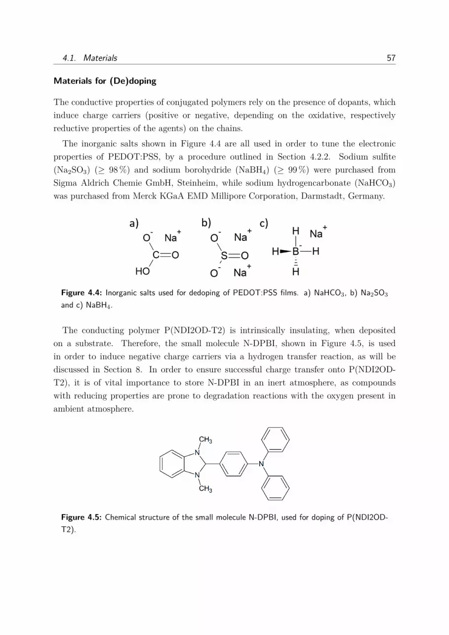
4.1. Materials 57
Materials for (De)doping
The conductive properties of conjugated polymers rely on the presence of dopants, whichinduce charge carriers (positive or negative, depending on the oxidative, respectivelyreductive properties of the agents) on the chains.
The inorganic salts shown in Figure 4.4 are all used in order to tune the electronicproperties of PEDOT:PSS, by a procedure outlined in Section 4.2.2. Sodium sulfite(Na2SO3) (≥ 98 %) and sodium borohydride (NaBH4) (≥ 99 %) were purchased fromSigma Aldrich Chemie GmbH, Steinheim, while sodium hydrogencarbonate (NaHCO3)was purchased from Merck KGaA EMD Millipore Corporation, Darmstadt, Germany.
Figure 4.4: Inorganic salts used for dedoping of PEDOT:PSS films. a) NaHCO3, b) Na2SO3
and c) NaBH4.
The conducting polymer P(NDI2OD-T2) is intrinsically insulating, when depositedon a substrate. Therefore, the small molecule N-DPBI, shown in Figure 4.5, is usedin order to induce negative charge carriers via a hydrogen transfer reaction, as will bediscussed in Section 8. In order to ensure successful charge transfer onto P(NDI2OD-T2), it is of vital importance to store N-DPBI in an inert atmosphere, as compoundswith reducing properties are prone to degradation reactions with the oxygen present inambient atmosphere.
Figure 4.5: Chemical structure of the small molecule N-DPBI, used for doping of P(NDI2OD-T2).

58 Chapter 4. Sample preparation
Ionic liquids (ILs)
Figure 4.6 shows the different ILs used for post-treatment of PEDOT:PSS, the resultsfor which are discussed in Chapter 7. 1-ethyl-3-methylimidazolium dicyanamide (EMIMDCA) (≥ 98.5 %) and 1-ethyl-3-methylimidazolium tetrafluoroborate (EMIM BF4) (≥97 %) were purchased from Sigma-Aldrich GmbH, while 1-ethyl-3-methylimidazolium tetra-cyanoborate (EMIM TCB) was purchased from Merck KGaA EMD Millipore Corporation,Darmstadt, Germany. All ILs are in liquid state at room temperature. For the investiga-tion in Chapter 7, it was ensured that the cation is the same, while the anion was varied.This allowed for better comparability of the results and helped with the deduction of theimprovement mechanism.
Figure 4.6: Ionic liquids used for the post-treatment of PEDOT:PSS films. a) EMIM DCA(green), b) EMIM TCB (orange) and c) EMIM BF4 (blue). The color code is also used for thewhole Chapter 7, in order to link the measured quantities with the respective ILs.
4.1.3 Substrate materials
For the largest part of this thesis standard microscopy slides made of soda-lime glass (CarlRoth GmbH & Co. KG, Darmstadt, Germany) of 1 mm thickness were used as substratesdue to their insulating properties. For neutron scattering experiments, p-doped siliconwafers (SiMat, Kaufering, Germany), with a thickness of 525µm, were cut into sizes of7 cm · 7 cm. These were polished on one side, exposing the (100) orientation. Both glassand silicon substrates were subjected to cleaning in an acid bath and plasma treatmentprior to film deposition, as described in Section 4.2.1.
FTO-coated glass substrates (FTO TEG 7/2.2) were used for the investigations ofP(NDI2OD-T2) in Chapter 8. They were purchased from SOLEMS S.A., Palaiseau,France.
Figure 4.7 shows two types of steel substrates used for IRT, which will be discussed inSection 3.1.5. Free-standing PEDOT:PSS films are suspended on both types of substratesin order to measure IRT using the substrate with small cavities, seen in Figure 4.7a, andto perform UV-Vis spectroscopy with the substrate with the large cavity in Figure 4.7b.

4.2. Thin film preparation 59
Figure 4.7: Schematic drawing of the steel substrates used for the transfer of free-standingPEDOT:PSS films. Substrate used for a) IRT with small cavities of varying sizes and for b)UV-Vis spectrscopy with larger cavity.
Since homogeneous films cannot be fabricated on these substrates because of the cavities,PEDOT:PSS films are transferred onto them with a procedure detailed in Section 4.2.3.
4.2 Thin film preparation
This section summarizes all the procedures involved in the fabrication of thermoelectricpolymer thin films. Thus, it comprises cleaning procedures for the substrates, as well asdifferent subsections detailing the involved procedures for the four projects discussed inthe results part of this thesis. Additionally, the fabrication procedure for a thermoelectricgenerator based on conducting polymers as active materials is described.
4.2.1 Substrate cleaning
Rigorous cleaning of substrates is crucial for the successful fabrication of thin films, sincethe interactions of substrates with the material to be deposited can largely influencethe homogeneity of the final film, as is also the case with impurities. Therefore, whenemploying glass or silicon substrates, all substrates were subjected to an acid bath, thecomponents for which are listed in Table 4.1. The water, hydrogen peroxide (30 %, CarlRoth GmbH Co. KG) and sulfuric acid ( to EMSURE, for analysis, Sigma-AldrichChemie GmbH, Steinheim, Germany) are mixed in the order given in the table, withthe mixture then being heated to 80 C. Since the temperature sensor cannot be placeddirectly into the acid, the temperature of a water bath heating the vessel containing theacid was controlled. After reaching the target temperature, the acid bath was allowedto take on the temperature of the water bath during an equilibration period of 15 min.The substrates were then placed in PTFE holders and submerged into the acid bath,while letting the cleaning take place for another 15 min. By washing the substrates withcopious amounts of deionized water, residues of the acid mixture were removed. The

60 Chapter 4. Sample preparation
wet substrates were then dried on a spin-coater (Delta 6 RT CC, Suss Microtech AG,Garching, Germany) at 1500 rpm for 30 s.
Table 4.1: Chemicals used for the preparation of an acid bath for substrate cleaning, with therespective amounts. [35]
Chemical Volume [mL]Deionized water 45
Hydrogen peroxide (30 %) 70Concentrated sulfuric acid 165
After acid cleaning, an oxygen plasma treatment was performed using a Plasma Sys-tem Nano (Diener Electronics). After applying vacuum inside the chamber, a definedpartial pressure for oxygen of 0.4 mbar is set, allowing for a continous oxygen flow whilesimultaneously applying vacuum in order to remove reaction products. For pure glassand silicon substrates, plasma powers of 250 W were applied for 10 min. For PDMS-coated glass substrates used for the preparation of free-standing PEDOT:PSS films, anincreased plasma power of 300 W was necessary. In all cases, the plasma treatment servesthe removal of organic residues on the substrate in addition to the hydrophilization ofthe glass/silicon/PDMS surfaces, respectively. This facilitated the wetting of the water-based PEDOT:PSS solution, and led to more homogeneous films. For the deposition ofhydrophobic P(NDI2OD-T2) solutions in DCB on glass substrates, the plasma treatmentwas omitted.
FTO substrates were cleaned by successively immersing them in four different solvents.These were the detergent Alconox (Sigma-Aldrich Chemie GmbH, Steinheim Germany),ethanol, acetone and isopropanol (all Rothipuran, ≥ 99.8%, Carl Roth GmbH Co. KG,Karlsruhe, Germany). This sequence allowed for an increasing hydrophobization of thesubstrate surface. Each step was performed for 10 min in an ultrasonic bath. Betweeneach step, the samples were rinsed with the next solvent in which they were about to beimmersed. After the cleaning procedure, the substrates were dried with a nitrogen gun.
4.2.2 PEDOT:PSS thin films
This section lays out a base process for the preparation of PEDOT:PSS solutions. Af-terwards, the different subsections refer to the thin film preparation procedures for thedifferent research projects.
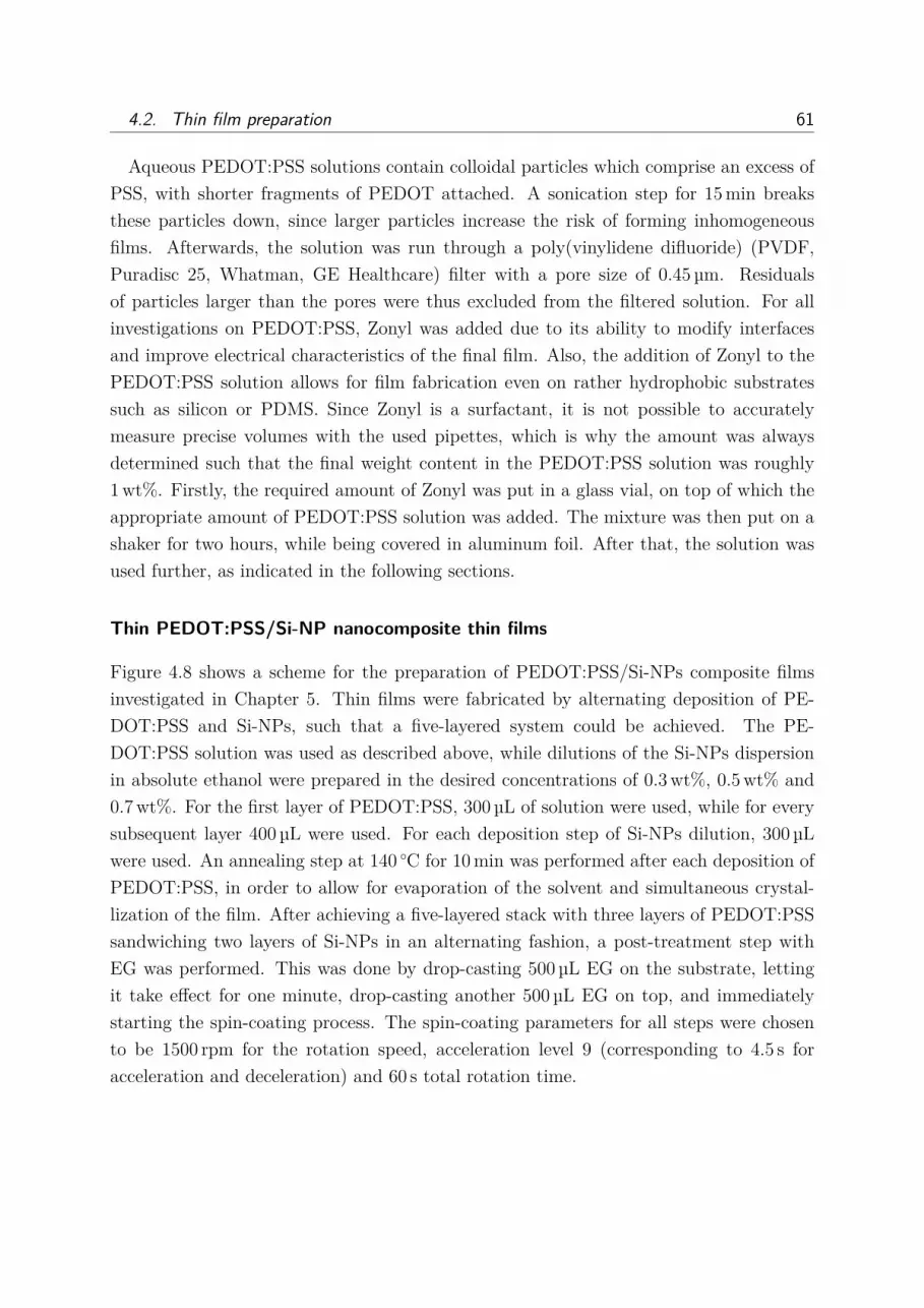
4.2. Thin film preparation 61
Aqueous PEDOT:PSS solutions contain colloidal particles which comprise an excess ofPSS, with shorter fragments of PEDOT attached. A sonication step for 15 min breaksthese particles down, since larger particles increase the risk of forming inhomogeneousfilms. Afterwards, the solution was run through a poly(vinylidene difluoride) (PVDF,Puradisc 25, Whatman, GE Healthcare) filter with a pore size of 0.45 µm. Residualsof particles larger than the pores were thus excluded from the filtered solution. For allinvestigations on PEDOT:PSS, Zonyl was added due to its ability to modify interfacesand improve electrical characteristics of the final film. Also, the addition of Zonyl to thePEDOT:PSS solution allows for film fabrication even on rather hydrophobic substratessuch as silicon or PDMS. Since Zonyl is a surfactant, it is not possible to accuratelymeasure precise volumes with the used pipettes, which is why the amount was alwaysdetermined such that the final weight content in the PEDOT:PSS solution was roughly1 wt%. Firstly, the required amount of Zonyl was put in a glass vial, on top of which theappropriate amount of PEDOT:PSS solution was added. The mixture was then put on ashaker for two hours, while being covered in aluminum foil. After that, the solution wasused further, as indicated in the following sections.
Thin PEDOT:PSS/Si-NP nanocomposite thin films
Figure 4.8 shows a scheme for the preparation of PEDOT:PSS/Si-NPs composite filmsinvestigated in Chapter 5. Thin films were fabricated by alternating deposition of PE-DOT:PSS and Si-NPs, such that a five-layered system could be achieved. The PE-DOT:PSS solution was used as described above, while dilutions of the Si-NPs dispersionin absolute ethanol were prepared in the desired concentrations of 0.3 wt%, 0.5 wt% and0.7 wt%. For the first layer of PEDOT:PSS, 300 µL of solution were used, while for everysubsequent layer 400 µL were used. For each deposition step of Si-NPs dilution, 300 µLwere used. An annealing step at 140 C for 10 min was performed after each deposition ofPEDOT:PSS, in order to allow for evaporation of the solvent and simultaneous crystal-lization of the film. After achieving a five-layered stack with three layers of PEDOT:PSSsandwiching two layers of Si-NPs in an alternating fashion, a post-treatment step withEG was performed. This was done by drop-casting 500µL EG on the substrate, lettingit take effect for one minute, drop-casting another 500µL EG on top, and immediatelystarting the spin-coating process. The spin-coating parameters for all steps were chosento be 1500 rpm for the rotation speed, acceleration level 9 (corresponding to 4.5 s foracceleration and deceleration) and 60 s total rotation time.

62 Chapter 4. Sample preparation
Figure 4.8: Sample preparation scheme for the fabrication of PEDOT:PSS/Si-NPs compositethin films, indicating the alternating fashion of deposition, with annealing steps in between.
Dedoped PEDOT:PSS thin films
The preparation of PEDOT:PSS dedoped with the inorganic salts NaHCO3, Na2SO3 andNaBH4 is shown in Figure 4.9. Aqueous solutions of the inorganic salts were prepared witha concentration of 1 M each. Small amounts were added to the PEDOT:PSS solution inorder to achieve different concentrations of dedopant, and afterwards subjected to shakingwhile covered in aluminum foil for 30 min. This ensured a complete reaction between thepolymer and the salt. Afterwards, two PEDOT:PSS layers were prepared on top of eachother by spin-coating with the parameters given above and annealing steps in between.Finally, EG post-treatment was applied as described previously, in order to study theeffects of the dedoping on the electronic structure of the films.

4.2. Thin film preparation 63
Figure 4.9: Sample preparation scheme for the fabrication of PEDOT:PSS films dedoped withinorganic salts. The mixing of aqueous salt solutions with the polymer solution prior to spin-coating is highlighted.
Post-treatment of PEDOT:PSS thin films with ionic liquids
In Figure 4.10, the fabrication process for IL-post-treated PEDOT:PSS films is shown.Direct mixing of PEDOT:PSS and IL leads to direct gelation of the polymer, which thencannot be processed into thin films with spin-coating anymore. Thus, an alternativeapproach was chosen, in which first a two-layered PEDOT:PSS film was prepared, withrotation speeds of 1500 rpm, acceleration level 9 for 60 s and two annealing steps in betweenat 140 C for 10 min. All ILs shown in Figure 4.6 were each dissolved in THF in different

64 Chapter 4. Sample preparation
Figure 4.10: Sample preparation scheme for IL-treated PEDOT:PSS films. In addition to thepost-treatment step with ILs dissolved in THF, the final washing step with pure THF is alsoshown.
concentrations and sonicated for 10 s prior to the post-treatment step. This was performedby drop-casting 400µL of the IL- solution, letting it take effect for one minute, thendrop-casting another 400µL, and immediately starting the spin-coating process. Anotherannealing step ensured the removal of residual THF. Still, due to their high boiling points,it was expected that the ILs could not removed from the films through annealing. Aftercharacterizing the films regarding their Seebeck coefficients and sheet resistances, the filmswere therefore subjected to a washing step with pure THF. This was done by drop-casting200 µL of pure THF, letting it take effect for one minute, spin-coating and annealing withthe same parameters as before. After the washing step the samples were subjected tothermoelectric characterization once again, in addition to UV-Vis spectroscopy, heightprofilometry and GIWAXS.

4.2. Thin film preparation 65
4.2.3 Free-standing PEDOT:PSS films
The preparation of free-standing films was necessary for the determination of the thermalconductivities of those films. There are methods to determine the thermal conductivityof thin films, such as time-domain thermoreflectance (TDTR). Since it relies heavily onthe observation of acoustic waves on the surface of the investigated thin films induced bythermal stress, metal layers are typically evaporated on the surface. There is a high riskfor damage in the film, due to e.g. diffusion of metal into the polymer, among others.Thus, we opted for IRT as alternative measurement technique.
The procedure for the preparation of free-standing PEDOT:PSS films is schematicallyshown in Figure 4.11. It was adopted from the work by Greco et al.. [36] Firstly, soda-limeglass substrates were cleaned as described in Section 4.2.1 and subjected to oxygen plasmatreatment. For the fabrication of a thin PDMS layer, first the mixture of oligomer andcross-linker had to be prepared. A weight ratio of 10 : 1 of oligomer to cross-linker waschosen. However, this mixture exhibits a very high viscosity which impedes the formationof a homogeneous thin film during spin- coating. Thus, 30 wt% of hexane were added to
Figure 4.11: Scheme of the procedure for the production of free-standing PEDOT:PSS films,highlighting the individual steps. Thin PDMS were prepared on clean glass substrates. Afterfabrication of PEDOT:PSS on top of the PDMS, a layer of PVA was drop-cast, in order tosupport the former upon removal from the PDMS substrate. Immersion of the PVA-supportedPEDOT:PSS into the water bath led to the dissolution of PVA, allowing for the transfer ofPEDOT:PSS onto the desired substrates for measurement of the thermal conductivity.

66 Chapter 4. Sample preparation
the oligomer/cross-linker mixture, followed by thorough mixing with a metal spatula. Themixture was deemed fluid enough when air bubbles in the mixture were visibly diffusingto the top of the vial. Immediately after plasma-treatment, 500 µL of the PDMS mixturewere spin-cast on the clean substrates at 2000 rpm, acceleration level 9 for 90 s, and thensubjected to annealing at 95 C for one hour.
After plasma-treatment at high power, as described in Section 4.2.1, the PDMS isfunctionalized with hydroxyl groups which allows for better wetting of the aqueous PE-DOT:PSS solution. It should be mentioned that addition of Zonyl is still crucial forhomogeneous film formation on PDMS. After the preparation of the PEDOT:PSS film,PVA was dissolved in deionized water such that the final concentration was 10 wt%.500 µL of the PVA solution were drop-cast on the films and allowed to dry overnight,while covered with a glass lid to avoid the setting of dust in the PVA layer. Lettingthe film dry overnight was necessary, as the water evaporated only very slowly from thefilm. PVA served as support for the PEDOT:PSS layer, after removal from the PDMS.PDMS possesses a low interfacial energy, which leads to weak adhesion of other materials.Thus, after cutting the film into desired shapes and sizes using a sharp razor blade, thePEDOT:PSS layer supported on PVA could be simply pulled from the PDMS substrateusing tweezers.
For the transfer of the PVA-supported PEDOT:PSS layer on the substrates needed forIRT, the setup shown in Figure 4.12 was used. It consists of a small glass container whichholds a bath of deionized water in which a beveled block made of aluminum or PTFEis submerged. A syringe pump is connected to the water bath via PTFE tubes. Aftersubmerging the PVA-supported PEDOT:PSS layer in the water bath, the PVA began todissolve while the PEDOT:PSS layer retained its shape and structural integrity. Thisallowed for the transfer of the PEDOT:PSS layer onto the metal substrates with thecavities. This was done by carefully agitating the free-standing PEDOT:PSS layer, suchthat it was located over the metal substrate, and then starting to drain out the waterusing the syringe pump. It was operated at a draining speed of 8 mL/min, in order toensure slow enough drainage allowing for sufficient time to re-adjust the film. Duringthe draining process, the film slowly set on top of the cavities. After careful removal ofthe block from the water bath, the substrate with the suspended film on top was slowlypushed to one edge of the block. After the substrate was removed from the block, thefilm was allowed to dry slowly in air, in order to avoid wrinkle formation, which couldimpede subsequent measurements. Afterwards, the obtained samples were subjected toIRT, UV-Vis spectroscopy and height profilometry.

4.2. Thin film preparation 67
Figure 4.12: Setup for the transfer of the PVA-supported PEDOT:PSS onto the desired sub-strate for IRT measurements, comprising a a glass container for the water bath, a beveledmetal/PTFE block, PTFE tubes and a syringe pump.
4.2.4 P(NDI2OD-T2) thin films
This section deals with the fabrication of P(NDI2OD-T2) films, the results for which arediscussed in Chapter 8 of this thesis. The preparation included the fabrication of dopedP(NDI2OD-T2) films on glass and FTO-coated glass substrates in various geometries,allowing for the investigation of the thermoelectric properties in-plane, cross-plane andpseudo-in-plane, all of which can be seen in Figure 4.13. In order to avoid degrada-tion of the doped P(NDI2OD-T2) in ambient atmosphere, all preparation steps includingthe preparation of the solutions, spin-coating and annealing steps were performed in anitrogen-filled glovebox.
For the fabrication of samples in in-plane geometry (seen in Figure 4.13), glass waschosen as substrate. As shown in Figure 4.14, both the P(NDI2OD-T2) and N-DPBI weredissolved separately in DCB at a concentration of 10 mg/mL each. Both solutions werethen stirred at 80 C for 30 min. A hydrophobic PTFE filter (Rotilabo, Carl Roth GmbHCo. KG, Karlsruhe, Germany) with a pore size of 0.45µm was used for removing largerparticles from the polymer solution. The latter was then mixed with the dopant solutionin order to obtain the desired dopant concentration. The mixture was again stirred at

68 Chapter 4. Sample preparation
80 C for two hours. This step is crucial, as it induces the doping through activation ofthe dopant molecule, as will be discussed later. For the spin-coating 200 µL of solutionwas used, after which the samples were annealed at 140 C. Aluminum electrodes werethen evaporated with areas of 2 mm · 15 mm at a distance of 10 mm. The defined areaand distance of the electrodes ensured comparability of the measurements.
The deposition process for cross-plane samples was similar. However, the FTO subtrateshad to be pre-treated by etching the FTO coating away partially. It was removed throughetching by applying zinc powder and hydrochloric acid on the respective areas on thesample using Q-tips, before the cleaning procedure described in Section 4.2.1. The etching,as well as the evaporation of the top aluminum electrode was done in such a way that theelectrode areas were 18 mm · 25 mm from opposite sides of the 25 mm · 25 mm substrate.Thus, an overlap area between the top and bottom electrode was achieved. In addition,the outermost 7 mm of the aluminum layer did not have an FTO coating underneath,which prevented short-circuits upon contacting with the copper tips. The opposite is truefor the side at which the FTO layed bare, since it was masked with PTFE tape prior tofilm deposition and electrode evaporation. The effective area in which the film is trulysandwiched between the electrodes amounted to 11 mm · 25 mm, which can also be seenin Figure 4.13. The polymer was applied by preparing solutions with concentrations of20 mg/mL and 10 mg/mL for the polymer and dopant, respectively, in order to achievethicker films and decrease the risk of short-circuits. Prior to the spin-coating of the dopedP(NDI2OD-T2) layer, the substrate was partially masked with PTFE tape. Annealingwas carried out as pointed out above.
Samples in the pseudo-in-plane geometry, also seen in Figure 4.13, were prepared in asimilar fashion to the cross- plane samples. The areas for the top and bottom electrodeswere each chosen to be 10 mm · 25 mm, while again having been placed at opposite edgesof the 25 mm · 25 mm substrate. This yielded an area of 5 mm · 25 mm which was only
Figure 4.13: Schematics of three different sample geometries for determination of thermo-electric properties of doped P(NDI2OD-T2) thin films in angular and cross-section perspective.The exemplary samples consist of glass substrates (gray boxes), FTO-coatings (yellow boxes),P(NDI2OD-T2) films (blue boxes) and aluminum electrodes (white boxes).

4.3. Thermoelectric generator based on conducting polymers as active materials 69
Figure 4.14: Scheme for the fabrication of P(NDI2OD-T2) films doped with N-DPBI. Afterdissolving polymer and dopant separately at elevated temperatures, they are combined at elevatedtemperatures in different ratios and spin-cast on substrates. A final annealing step is performedin order to induce crystallization.
covered by the polymer film. The lack of overlap between the top and bottom electrodeled to the prevention of short-circuits. Charge transport in this geometry was expectedto primarily occur in lateral direction, since macroscopic distances have to be covered asopposed to the film thickness in the range of nanometers. In general, the cleaning andfilm fabrication were performed as described above.
4.3 Thermoelectric generator based on conductingpolymers as active materials
The investigation of P(NDI2OD-T2), led to its choice as potential candidate as n-type legin a thermoelectric generator based on conducting polymers as active materials. Due to itsfavorable properties, which are discussed in Chapter 8, the pseudo-in-plane geometry wasadopted for both N-DPBI-doped P(NDI2OD-T2) as n-type and EG-treated PEDOT:PSSas p-type leg. A schematic for the fabrication process is shown in Figure 4.15.
Firstly, a large sheet of FTO-coated glass was cut into substrates of 25 mm · 50 mm.

70 Chapter 4. Sample preparation
Figure 4.15: Schematic for the fabrication of a thermoelectric generator based on P(NDI2OD-T2) and PEDOT:PSS. Through selective masking with PTFE band, defined areas of the p-typeand n-type legs can be achieved. After fabricating the p-type leg in ambient atmosphere, thesubstrates are transferred into a nitrogen-filled glovebox to fabricate the n-type leg. Both legsare electrically bridged by the aluminum top electrode in the center, while the FTO electrodesat both ends of the substrate are used for contacting during measurement.
Large parts of the FTO-coating were etched away, as described above, such that areasof 10 mm · 25 mm remained covered with FTO on both ends of the substrate. Throughmasking of the substrate with PTFE band, an area of 13 mm · 25 mm was firstly coveredwith PEDOT:PSS and subjected to annealing at 140 C for 10 min. An overlap area of3 mm · 25 mm with the bottom FTO electrode ensured electrical contactability. Post-treatment with EG was performed by again drop-casting 1 mL in two steps, as describedabove. After spin-coating at 1200 rpm for 60 s, annealing at 140 C was again performed for10 min. This then became the p-type leg of the generator. Before transfer into a nitrogen-filled glovebox, the PEDOT:PSS-covered part of the substrate was again masked with

4.3. Thermoelectric generator based on conducting polymers as active materials 71
PTFE band. P(NDI2OD-T2) films were fabricated in the same fashion as the samplesin pseudo-in-plane geometry described above, leaving blank space in the center of thesubstrate. As a last step, the top aluminum electrode, with an area of 16 mm · 25 mm wasevaporated onto the center of the substrate, with an overlap area of 3 mm · 25 mm withboth legs. Thereby, a closed circuit could be obtained by contacting the FTO electrodeson both ends of the substrates.


5 Nanostructuring of PEDOT:PSS thinfilms with silicon nanoparticles forenhancement of thermoelectricproperties
The article ’Morphology-Function Relationship of Thermoelectric Nanocomposite Filmsfrom PEDOT:PSS with Silicon Nanoparticles’ (N. Saxena et al., Adv. Electron. Mat., 3,1700181, 2017, DOI: 10.1002/aelm.201700181) is largely based on results shown in thischapter. [2]
The emergence of organic thermoelectrics in recent years is in large part owed to thedecades of research which went into the synthesis and characterization of inorganic ther-moelectric materials, which usually consist of elements such as bismuth, tellurium, silicon,germanium, selenium, sulfur, etc. [37] Up to the 1990s, it was believed that the highestachievable value for ZT would be close to 1, due to the interdependence of S, σ and κ tothe charge carrier concentration, since experiments did not yield higher values. [38] Thefact that theory did not pose such strict limits puzzled researchers and led to ground-breaking research by Hicks and Dresselhaus et al., who found drastic changes in thermo-electric properties for lower dimensionalities of nanostructured Bi2Te3. [1] They ascribedthe found trends to changes in the density of states (DOS), and increase in the phononsurface scattering, while also highlighting the increase in ZT upon stronger confinement.This incentivized other approaches at optimizing ZT, which for the most part focused ondecreasing the thermal conductivity. Due to the electronic contribution to the thermalconductivity being linked to the electrical conductivity via the Wiedemann-Franz law (seeEquation 2.13), it is difficult to decouple it from the other thermoelectric quantities. Inorder to lower the lattice thermal conductivity of a system, it is necessary to introducegrain boundaries from which phonons can be scattered. This can be done in a top-downapproach by e.g. ball-milling, or in a bottom-up approach through chemical synthesisof nanoparticles. Also methods like introduction of superstructures or heteroatoms seem
73

74Chapter 5. Nanostructuring of PEDOT:PSS thin films with silicon nanoparticles for
enhancement of thermoelectric propertiespromising regarding increase of phonon scattering for reduction of the phonon contribu-tion to the thermal conductivity. [37]
Drawing an analogy to organic thermoelectrics, preparing inorganic-organic compositethin films appears to be a viable solution. For example, Yee et al. synthesized hybridtellurium nanowires assisted by PEDOT:PSS and prepared composites with PEDOT:PSSdoped with EG and dimethyl sulfoxide (DMSO). [39] The combination of the intrinsicallyhigh Seebeck coefficient of tellurium, combined with an apparent increase in ordering ofPEDOT chains in vicinity of the Te nanowires leading to improved electrical conductivi-ties, ultimately yielded higher power factors of more than 100WK−2m−1. This idea wasimproved upon by Bae et al. through a simple treatment of the Te/PEDOT:PSS hy-brid composite films with sulfuric acid. [40] The drastic increase in electrical conductivityup to 5000 S/cm therefore led to power factors of up to approximately 300WK−2m−1.Yan et al. took a different route in sandwiching post-treated, highly conductive PE-DOT:PSS layers of different thicknesses in between aluminum electrodes. As an explana-tion for the increased Seebeck coefficients, the authors discussed phonon scattering at themetal/polymer interfaces through acoustic mismatch, even though in this specific casethey did not make statements about potential changes in the electrical conductivity.
This part of the work deals first and foremost with the influence of Si-NPs on thethermoelectric properties of nanocomposite thin films with PEDOT:PSS. This hybridnanostructuring approach is expected to yield a decrease of the phonon contributionto the thermal conductivity due to phonon scattering off of the Si-NPs. Two differentfabrication routes for composite films are analyzed and evaluated using TOF-GISANS. Inone instance, PEDOT:PSS and Si-NPs are deposited separately on a substrate in a layer-by-layer fashion, whereas in the other instance Si-NPs are mixed with the polymer solutionprior to deposition. TOF-GISANS allows for the determination of lateral structures andfor analysis of the composition by investigating the SLD profiles of the samples andcomparing to theoretical values. After deciding on one fabrication route, PEDOT:PSS/Si-NPs composite films are characterized regarding their thermoelectric properties, includingthe thermal conductivity measured by IRT, in order to calculate the full figure of meritZT. Additionally, GIR-TeXS is employed for the elucidation of structural changes uponintroduction of different amounts Si-NPs and also for the discovery of a morphology-function relationship.
5.1 Selection of a fabrication route
Figure 5.1 compiles exemplary 2D TOF-GISANS scattering patterns for PEDOT:PSS/Si-NPs composite films prepared in the layer-by-layer and mixing approach, respectively.

5.1. Selection of a fabrication route 75
Figure 5.1: Selected 2D TOF-GISANS scattering patterns of PEDOT:PSS/Si-NPs compositefilms prepared by the a) layer-by-layer and b) mixing approach. Average wavelengths of therespective images are given below the scattering patterns in Angstrom. The specular peak (S),Yoneda peak (Y) and direct beam (D) covered by a beam stop are marked exemplarily.
For both approaches, the concentration of Si-NPs is set to 0.7 wt%. While the obtainedscattering patterns clearly differ for both approaches, the Yoneda peak shifts in z-directiontowards larger angles as function of wavelength. For the mixing approach, the Yoneda andspecular peaks extend in z-direction irrespective of λ, hinting at an increased roughnessof the sample.
Horizontal line cuts are extracted for both samples for the different wavelengths, in orderto obtain information on the lateral structure. These are shown in Figure 5.2, togetherwith the corresponding model curves. One of the main advantages of TOF-GISANS is theaccessible q-range which shifts towards lower values with increasing wavelength. This isaccounted for in the modeling of the scattering curves. The model includes three distinctfamilies of spherical structures which are arranged in a one-dimensional paracrystallinelattice. Parameters such as the average sizes of objects and their average center-to-centerdistances with the respective distributions are chosen in a way that for a single sampleall the scattering curves can be modeled with a single set of parameters. Variations inthe intensity are to be expected as the neutron flux is different for different wavelengths.Qualitatively, the curves for the two samples differ in their shape, hinting at changes inthe morphology due to the different fabrication routes.
As mentioned above, after modeling of the scattering curves, structural parameters ofthe two samples can be extracted and compared, the results for which can be seen inFigure 5.3. The notion that preparation of the samples by different fabrication routesleads to a different morphology is evident from close investigation of the parameters. Forthe sample prepared in the layer-by-layer approach, the radii of the spherical structures are180 nm, 100 nm and 60 nm, representing large, medium and small structures, respectively.The mixing approach yields in general spherical structures with smaller radii, namely150 nm, 80 nm and 10 nm. Another aspect is the center-to-center distance of the sphericalstructures, which is represented by the structure factor in Figure 5.3b. In the layer-by-

76Chapter 5. Nanostructuring of PEDOT:PSS thin films with silicon nanoparticles for
enhancement of thermoelectric properties
Figure 5.2: Horizontal line cuts for PEDOT:PSS/Si-NPs composite films prepared in a a) layer-by-layer (dark yellow) and b) mixing (orange) approach. Modeled curves are shown in black.The curves are stacked vertically for clarity of presentation, with increasing wavelength. Foreach sample one set of structural parameters was found, with which the scattering curves couldbe modeled.
layer case, the values are 370 nm, 300 nm and 250 nm, whereas the mixing approach yieldsvalues of 400 nm, 200 nm and 150 nm.
The spherical structures can be discussed in terms of radius distributions and the num-ber of domains. The size distributions for both preparation procedures are shown inFigure 5.4. It represents the distribution of domains as function of size, whereas theamplitude for a given domain size represents the corresponding number of domains ofthat specific size. The relation between the size of a domain, the scattering intensity andthe number of domains can be understood when referring to Equations 2.25 and 2.26.Therewith, it can be seen that the scattering intensity is proportional to both the volumeof a domain or the number of domains with a given size. Consequently, by extracting the

5.1. Selection of a fabrication route 77
Figure 5.3: a) Structure radii and b) structure distances obtained from horizontal line cuts ofTOF-GISANS measurements for PEDOT:PSS/Si-NPs composite films prepared in a layer-by-layer (LBL, dark yellow) and mixing (mix, orange) approach. Three distinct structural familieswere included in the modeling, referred to as large (triangles), medium (circles) and small(square) structures.
scattering intensity for each contribution from the model and dividing by the volume ofthe domain, the number of domains can be obtained.
Upon closer investigation of Figure 5.3, one can then immediately understand the largenumber of small domains obtained with the mixing approach. In order to compensatefor the small scattering volume, a large number of small domains is required to achieve acertain scattering intensity. This also explains the decreasing amplitude observed for themedium and large structures, as in those cases the relatively larger scattering volume leadsto a larger scattering intensity. In general, the notion that the layer-by-layer approachyields overall larger structures, as is also shown in Figure 5.3a, is also evident here.When regarding the morphology of PEDOT:PSS/Si-NPs composite films in terms of theirpotential thermoelectric capabilities, the former is deemed more favorable the larger thedomains are. PEDOT:PSS is known to phase-separate upon deposition on a substrate,yielding PEDOT-rich domains with thin PSS-rich shells. [41] The PSS-shell presents abarrier for charge-transport, making the reduced surface area through increased domainsizes obtained from the layer-by-layer approach more promising with respect to chargetransport within the film.
TOF-GISANS offers two distinct advantages compared to x-ray scattering. Firstly, the

78Chapter 5. Nanostructuring of PEDOT:PSS thin films with silicon nanoparticles for
enhancement of thermoelectric properties
Figure 5.4: Analysis of domain size distribution for PEDOT:PSS/Si-NPs composite films pre-pared in a layer-by-layer (dark yellow) and mixing (orange) approach. The values are normalizedto those of the respective large domain radii, obtained from the analysis of horizontal cuts ofthe TOF-GISANS measurements.
direct proportionality of the critical angle to the neutron wavelength and, more impor-tantly, secondly, the ability of performing the measurement in the time-of-flight mode.The latter allows for collection of scattering patterns originating from different neutronwavelengths in a single measurement. By monitoring the position of the Yoneda peak inthe vertical cuts seen in Figure 5.5a and 5.5b, correcting for the incident angle and plottingit as function of wavelength, a linear fit can be performed, as is done in Figure 5.5c. Fromthe slope the SLD can be extracted according to Equation 3.19, which gives insight intothe chemical composition of the probed samples. An increased SLD of 1.80 · 10−6 A−2 isobtained for the PEDOT:PSS/Si-NPs composite prepared in the layer-by-layer approach,compared to 1.42 · 10−6 A−2 for the mixing approach. With the knowledge of the SLD foreach of the film components, namely PEDOT, PSS and the Si-NPs, the obtained SLDvalues can be put into perspective.
In comparison to the reference values for each component given in Table 5.1, one canobserve that the SLD value obtained for layer-by-layer sample is significantly larger thanthe one for pure PEDOT. On the other hand, the SLD value for sample prepared inthe mixing approach closely resembles that of pure PSS. Two possible conclusions can

5.1. Selection of a fabrication route 79
Figure 5.5: Vertical line cuts extracted from 2D TOF-GISANS data of for different wavelengths,shown for PEDOT:PSS/Si-NPs composite films in the a) the layer-by-layer and b) mixing ap-proach. c) Critical angle values αc as function of neutron wavelength for PEDOT:PSS/Si-NPsprepared in a layer-by-layer (dark yellow) and mixing (orange) approach. The critical angle valuesare corrected for the incident angles, also taking gravity effects into account. Solid lines in therespective colors are linear fits from which the SLD can be calculated. Extracted values obtainedfrom the slopes of the linear fits are given additionally.
be drawn from this. Firstly, the inclusion of Si-NPs into the composite film appearsto be more efficient in the layer-by-layer approach than for the mixing approach, asthe SLD of the Si-NPs is larger than for pure PEDOT, thus leading to an increasedoverall SLD for the composite. Nominally, the same amount of Si-NPs was employedfor both fabrication routes, which hints at differences in the film formation. This most

80Chapter 5. Nanostructuring of PEDOT:PSS thin films with silicon nanoparticles for
enhancement of thermoelectric properties
Table 5.1: SLD values for PEDOT, PSS and Si.
material SLD (A−2)PEDOT 1.71 · 10−6
PSS 1.42 · 10−6
Si 2.07 · 10−6
H2O −5.61 · 10−6
likely originates from the nature of the Si-NPs, which are known and expected to carrya silicon oxide shell in ambient atmosphere. [42] The rather hydrophobic nature of theSi-NPs, requires a more organic solvent like ethanol, in order for them to fully disperseand prevent aggregation. Upon introduction into the aqueous PEDOT:PSS solution, it isconceivable that they aggregate and subsequently cannot be processed properly anymore.This was also observed from visual inspection of the solution after introduction of Si-NPs, which showed signs of aggregation. In the layer-by-layer approach, this problem iscircumvented, since the Si-NPs do not come in contact with the aqueous solvent, but areinstead deposited on annealed PEDOT:PSS.
A possible explanation for the drastically lower SLD obtained for the sample preparedin the mixing approach can be given, considering the ability of the PSS-component of PE-DOT:PSS films to absorb water from the atmosphere, leading to subsequent swelling. [43]As both the sample preparation and the TOF-GISANS measurements were performed inambient atmosphere, a certain degree of swelling and thus presence of water in the com-posite films is to be expected. The negative SLD of light water (H2O) of −5.61 · 10−6 A−2
would thus lead to a decrease of the SLD of both samples, with the case of the mixingapproach being more severe due to the less efficient inclusion of Si-NPs.
Thus it can be concluded that, from a structural point of view, the layer-by-layerroute for the fabrication of PEDOT:PSS/Si-NPs composite films is superior to the mixingapproach. TOF-GISANS revealed a more favorable morphology due to larger domainsobtained in the layer-by-layer fabrication, as well as a more efficient inclusion of Si-NPsinto the film due to prevention of aggregation. Therefore, the layer-by-layer fabricationwill be used in the following for the investigation of changes in thermoelectric propertiesas function of Si-NPs concentration.
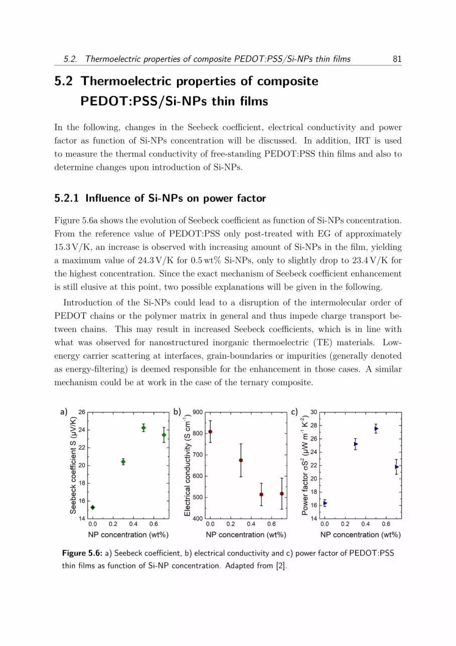
5.2. Thermoelectric properties of composite PEDOT:PSS/Si-NPs thin films 81
5.2 Thermoelectric properties of compositePEDOT:PSS/Si-NPs thin films
In the following, changes in the Seebeck coefficient, electrical conductivity and powerfactor as function of Si-NPs concentration will be discussed. In addition, IRT is usedto measure the thermal conductivity of free-standing PEDOT:PSS thin films and also todetermine changes upon introduction of Si-NPs.
5.2.1 Influence of Si-NPs on power factor
Figure 5.6a shows the evolution of Seebeck coefficient as function of Si-NPs concentration.From the reference value of PEDOT:PSS only post-treated with EG of approximately15.3 V/K, an increase is observed with increasing amount of Si-NPs in the film, yieldinga maximum value of 24.3 V/K for 0.5 wt% Si-NPs, only to slightly drop to 23.4 V/K forthe highest concentration. Since the exact mechanism of Seebeck coefficient enhancementis still elusive at this point, two possible explanations will be given in the following.
Introduction of the Si-NPs could lead to a disruption of the intermolecular order ofPEDOT chains or the polymer matrix in general and thus impede charge transport be-tween chains. This may result in increased Seebeck coefficients, which is in line withwhat was observed for nanostructured inorganic thermoelectric (TE) materials. Low-energy carrier scattering at interfaces, grain-boundaries or impurities (generally denotedas energy-filtering) is deemed responsible for the enhancement in those cases. A similarmechanism could be at work in the case of the ternary composite.
Figure 5.6: a) Seebeck coefficient, b) electrical conductivity and c) power factor of PEDOT:PSSthin films as function of Si-NP concentration. Adapted from [2].

82Chapter 5. Nanostructuring of PEDOT:PSS thin films with silicon nanoparticles for
enhancement of thermoelectric propertiesAnother feasible explanation for the increase could be given assuming a non-negligible
Seebeck coefficient of the Si-NPs themselves. It is conceivable that they are subjectedto the temperature gradient themselves and generate an electrical potential accordinglywhich simply adds to the one of the PEDOT:PSS. This can explain the increase up toconcentrations of 0.5 wt% . However, the slight drop in Seebeck coefficient for concentra-tions of 0.7 wt% would then have to be explained in terms of size changes of nanoparticleclusters. As Chen et al. found, the Seebeck coefficient of particles is inversely correlatedto their respective size. [44] Drawing an analogy to the present case, this suggests ag-gregation of Si-NPs which would lead to increased effective sizes and therefore to lowerintrinsic Seebeck coefficients.
While both approaches at understanding the effects are reasonable, the discovery of thetrue enhancement mechanism is subject to further investigation.
Nevertheless, the introduction of Si-NPs the polymer films appears to also have impli-cations on the electrical conductivity, as can be seen in Figure 5.6b. Increasing concen-trations of Si-NPs have an adverse effect on the electrical conductivity, since it decreasesfrom 809 S/cm for the reference film without Si-NPs to 517 S/cm for the highest concen-tration. This is easily understood, considering that the single-crystalline Si-NPs carry aninsulating shell of silicon dioxide of few nanometers thickness. [34] The notion that theythusly do not contribute to the conductivity of the composite film, but instead disturb thesemicrystalline order of the PEDOT:PSS matrix is also supported by the first explanationgiven above for the enhancement of the Seebeck coefficient. The incorporation of Si-NPswould hinder charge transport most likely between or within conducting, PEDOT-richdomains, which is macroscopically measured as drop in electrical conductivity.
Combining both the Seebeck coefficient and the electrical conductivity, the power factorσS2 can be calculated, as shown in Figure 5.6c. The steady increase from values of16.4 WK−2m−1 for the reference up to 27.6 WK−2m−1 for 0.5 wt% Si-NPs concentrationis for the most part governed by the changes in the Seebeck coefficient. The drop whichwas seen for the latter at Si-NPs concentrations of 0.7 wt% is even more prominent for thepower factor, due to its square dependence on the Seebeck coefficient. For that specificsample a power factor of 21.8 WK−2m−1 is obtained.
In summary, Si-NPs can be used to enhance the TE capabilities of PEDOT:PSS beyondeither of the constituents, mainly due to the increase in Seebeck coefficient which mostlikely stems from the semiconducting nature of the Si-NPs themselves. At an optimalconcentration of 0.5 wt%, the power factor is roughly improved by a factor of 1.3. As anext step, IRT is used in order to measure the thermal conductivity of PEDOT:PSS asfunction of Si-NPs concentration.

5.2. Thermoelectric properties of composite PEDOT:PSS/Si-NPs thin films 83
5.2.2 Measurement of thermal conductivity: Infrared thermography
Many techniques for the measurement of thermal conductivities exist, such as TDTR, the3ω-method, etc. [45,46] However, they often pose strict constraints on sample geometriesor their film properties such as low roughness, etc. Especially for TDTR, a thin metallayer has to be fabricated on top of the film by lithography, potentially altering the latter’sstructure. [47] Additionally, the films have to be suspended on a substrate, which mightaffect the measured thermal conductivity due to its large thickness discrepancy to thefilm to be investigated. IRT is a method which was co-developed in the framework of thisthesis, and is thus the technique of choice. It allows for the contact-free measurementof the thermal conductivity on films which are suspended on steel substrates with smallspherical cavities. On top of these cavities, the film is actually free-standing, thereforerendering the obtained values more accurate. Exemplary optical and infrared micrographsof a PEDOT:PSS films suspended on a steel substrate with spherical cavities are shownin Figure 5.7.
Exemplary infrared micrographs for the composite PEDOT:PSS/Si-NPs films with dif-ferent concentrations of the latter are shown in Figure 5.8. For the discussion of themicrographs, it is useful to refer to the principle of IRT which is schematically shown inFigure 3.7. The free-standing sections of the suspended thin films are illuminated via a redlight-emitting diode and subsequently thermally excited. Depending on their respectivein-plane thermal conductivity, the heat is either dispersed through emission of infraredradiation or through heat conduction to the steel substrate, which acts as heat sink. Thefact that qualitative differences between the different images can be discerned, is already
Figure 5.7: a) Optical micrograph of PEDOT:PSS film suspended on steel substrate withspherical cavities of different sizes. b) Infrared micrograph of film upon thermal excitation withvisible light. Larger amplitudes of thermal radiation are represented by the transition from blackto white.

84Chapter 5. Nanostructuring of PEDOT:PSS thin films with silicon nanoparticles for
enhancement of thermoelectric properties
Figure 5.8: Infrared thermographs of PEDOT:PSS films a) without Si-NPs, b) 0.3 wt% Si-NPs,c) 0.5 wt% Si-NPs and d) 0.7 wt% Si-NPs suspended on a cavity of 0.3 mm diameter on astainless steel holder and the corresponding temperature scale. Taken from [2].
a first indication that the thermal conduction properties are modified by the presence ofthe Si-NPs.
In decreasing order, the largest temperature increases are found for the reference samplewithout Si-NPs, followed by 0.7 wt%, 0.5 wt% and 0.3 wt%. This indicates a correspondingincrease in the values for κ. With the correction for the film thickness d and the absorbedareal power density pabs according to Equation 3.11, the thermal conductivity as functionof Si-NPs can be obtained, the results for which are shown in Figure 5.9.
A thermal conductivity of approximately 1 Wm−1K−1 for PEDOT:PSS post-treatedwith EG fits well to the results of Wei et al. [48] Surprisingly, non-linear changes areobserved with increasing Si-NPs amount. A maximum of 1.37 Wm−1K−1 is observed at0.3 wt%, which subsequently drops again to 0.97 Wm−1K−1 for the highest concentra-tion of 0.7 wt%. This unexpected behavior will be explained below, in the discussion ofmorphology changes deduced from SEM and GIR-TeXS.
5.2.3 Calculation of full figure of merit ZT
Nevertheless, with the measurement of all relevant thermoelectric quantities, namely See-beck coefficient, electrical conductivity and thermal conductivity, as function of Si-NPsconcentration, the full figure of merit ZT can be calculated. It can be seen in Figure 5.10.

5.2. Thermoelectric properties of composite PEDOT:PSS/Si-NPs thin films 85
Figure 5.9: Thermal conductivity of PEDOT:PSS films as function of Si-NP concentration, asdetermined from IRT.
The increasing trend of ZT follows for the most part that of the Seebeck coefficientwith increasing Si-NPs concentration. While for the reference film without Si-NPs a ZTvalue of roughly 0.005 is achieved, the maximum value of 0.008 is found for a Si-NPsconcentration of 0.5 wt%. The subsequent slight drop can be explained with the dropin the Seebeck coefficient, which enters into Equation 2.7 squared. It can be concludedthat the enhancement of ZT originates from a combination of different factors. Firstly,the Seebeck coefficient is enhanced up to intermediate concentrations. Secondly, while theintroduction of Si-NPs with their insulating oxide shell is detrimental to the overall electri-cal conductivity of the films, it is still sufficiently high. Thirdly, even though the thermalconductivity increases for low amounts of Si-NPs, further addition yields values close tothat of the reference film. The improvement of ZT by a factor of roughly 1.5 renders thehybrid nanostructuring approach feasible regarding improvement of thermoelectric prop-erties, especially since IRT is a viable method for measuring and understanding potentialimplications thereof on the thermal conductivity.

86Chapter 5. Nanostructuring of PEDOT:PSS thin films with silicon nanoparticles for
enhancement of thermoelectric properties
Figure 5.10: Full figure of merit ZT of PEDOT:PSS films with varying concentrations of Si-NPs,calculated for an average temperature of 330 K. Adapted from [2].
5.3 Morphological properties of compositePEDOT:PSS/Si-NPs thin films
After establishing the feasibility of the nanostructuring approach of PEDOT:PSS with Si-NPs, the next step is to understand how the presence of the latter affects the morphologyof the composite films and if a link to the observed thermoelectric properties can befound. For this purpose, SEM is used as a real-space technique to investigate the surfacestructure of the composite films. Additionally, the bulk structure of the ternary compositefilms is studied with GIR-TeXS. As will be discussed below, GIR-TeXS offers a range ofadvantages over a classical GISAXS experiment regarding the ability to assign structuralfeatures to the different components.
5.3.1 Real-space morphology: scanning electron microscopy
Electron micrographs of the PEDOT:PSS/Si-NPs composite films are shown in Figure5.11 as function of nanoparticle concentration. For the reference PEDOT:PSS film shownin Figure 5.11a, features with both high and low intensity can be seen in the micrograph.

5.3. Morphological properties of composite PEDOT:PSS/Si-NPs thin films 87
These correspond to PEDOT and PSS, respectively, as they exhibit different electricalconductivities. Upon increase of the Si-NPs concentration to 0.3 wt%, larger structuresemerge. Notably, no individual Si-NPs are visible, even though they should be resolvablewith their sizes in the range of 30 nm. This might originate from the preparation ofthe composite films outlined in Section 4.2.2. Alternating deposition of PEDOT:PSSand Si-NPs may lead to burying of the latter beneath a polymer layer, explaining whythey cannot be seen in the top-view electron micrographs. Even for concentrations up to0.7 wt%, no Si-NPs can be discerned.
This notion is supported when looking at the radial power spectral densities (RPSDs)shown in Figure 5.12. Compared to the PEDOT:PSS film without Si-NPs, all other sam-ples show an increased RPSD intensity at small q-values which indicates morphologicalrearrangement due to the emergence of larger structures, which is induced by the intro-duction of Si-NPs. Notably, the intensity at small q-values is largest for concentrations of0.3 wt% and 0.7 wt%, which also exhibit large structures in the micrographs. It can thusbe concluded that SEM by itself is insufficient to understand the structural impact of theSi-NPs. In the following, the analysis of GIR-TeXS data will shed light on changes in thebulk morphology of the PEDOT:PSS/Si-NPs films.
Figure 5.11: Scanning electron micrographs of PEDOT:PSS films a) without Si-NPs, b) 0.3 wt%Si-NPs, c) 0.5 wt% Si-NPs and d) 0.7 wt% Si-NPs. Taken from [2].

88Chapter 5. Nanostructuring of PEDOT:PSS thin films with silicon nanoparticles for
enhancement of thermoelectric properties
Figure 5.12: Radial power spectral density curves extracted from 2D fast Fourier transformimages, obtained from scanning electron micrographs of PEDOT:PSS films without Si-NPs(black), 0.3 wt% Si-NPs (red), 0.5 wt% Si-NPs (blue) and 0.7 wt% Si-NPs (magenta). Takenfrom [2].
5.3.2 Grazing-incidence resonant tender x-ray scattering
The discussion of the GIR-TeXS data for the elucidation of the structure of PEDOT:PSS/Si-NPs films will follow the workflow layed out in Section 3.3.3. It is therefore divided intodiscussion of NEXAFS data, the modeling of horizontal line cuts from the 2D scatteringpatterns, calculation of the energy-dependent scattering contrast and lastly the elucida-tion of a morphological model and its correlation to thermoelectric properties.
Near-edge x-ray absorption fine structure (NEXAFS): calculation of β and δ
As mentioned above, the strength of GIR-TeXS is its ability to distinguish components ofsimilar electron density by employing incident x-ray energies which match core electrontransitions of constituent atomic species. In this case, measurements are performed at thesulfur K-edge, located at approximately 2473 eV. [49] The high sensitivity for chemicalshift of a NEXAFS measurement makes it possible to distinguish the main polymericcomponents PEDOT and PSS. As can be seen in Figure 2.3, both parts of the blendare sulfur-containing. However, in the case of PEDOT the sulfur is bound within thethiophene group, while in PSS it is surrounded by three oxygen atoms. Despite thesimilar chemical composition, their absorption behavior at the sulfur K-edge is expectedto differ according to the atomic configuration. In contrast, the Si-NPs are not expected toshow any non-linearities in their optical behavior, as they do not contain sulfur. NEXAFS

5.3. Morphological properties of composite PEDOT:PSS/Si-NPs thin films 89
Figure 5.13: Real part δ (solid symbols) and imaginary part β (hollow symbols) of refractiveindex for a) PEDOT, b) PSS and c) Si-NPs, as determined from NEXAFS measurements at thesulfur K-edge and using the Kramers-Kronig relations. Taken from [2].
measurements are performed on the three individual components as described in Section3.2.4, in order to extract values for the imaginary part of the refractive index β, as functionof energy. In turn, the latter can be used to calculate the corresponding values for thereal part of the refractive index δ using the Kramers-Kronig relations shown in Equations2.29 and 2.30.
In a NEXAFS measurement, the mass absorption coefficient is obtained, which givesinsight into the fine structure of a material close to a core electron resonance. TheHenke database lists atomic scattering form factors f, which then allows for calculationof optical properties according to Equation 2.20. However, the fine structures stronglydiffer from molecule to molecule, and thus have to be measured separately. Similarly toa UV-Vis measurement, the energy of the x-ray beam incident on the sample is tuned,while simultaneously detecting the absorbed fraction of light. is then calculated usingEquation 3.16. The latter can be transformed into the imaginary part of the refractive

90Chapter 5. Nanostructuring of PEDOT:PSS thin films with silicon nanoparticles for
enhancement of thermoelectric propertiesindex n β with Equation 2.28. The Kramers-Kronig relations in Equations 2.29 and 2.30link β to the real part of the refractive index δ, which is not easily measurable. In thiscase, the freely available software package KKcalc is used for the calculation of δ.
The obtained spectra are shown in Figure 5.13. Drastic differences in the spectra forthe different components can be seen immediately. Most significantly, PEDOT exhibitsa strong absorption peak located very close to the sulfur K-edge in both the curves for δand β, as seen in Figure 5.13. This signal originates from the resonance of the x-ray beamwith the thiophene sulfur found in PEDOT. In contrast, PSS shows no such non-linearitiesclose to the sulfur K-edge. Instead, a strong signal is located at roughly 2480 eV, and thusnot covered by the GIR-TeXS measurements. Most likely, this can be assigned to thesulfur found in the sulfonate group, surrounded by three oxygen atoms. As expected,the Si-NPs show no non-linearities in their optical response, due to the absence of sulfur.However, the order of magnitude for the δ- and β-values is still comparable to that foundfor PEDOT and PSS.
From the obtained values for δ and β as function of energy, the scattering contrast canbe inferred according to Equation 2.31.
Grazing-incidence small-angle scattering (GISAXS): lateral structure
As described in Section 2.3.1, 2D GISAXS patterns can be analyzed in two differentways. A vertical line cut contains information on the existing chemical components inthe investigated material, which can be differentiated with their respective critical angles,in addition to vertical correlation. A horizontal line cut on the other hand containsinformation on the presence of mesoscopic structures and their lateral correlation, i.e.their arrangement in the plane of the substrate. The sizes and shapes of structures, aswell as their arrangement are extracted from the horizontal cuts through modeling in theframework of the DWBA.
PEDOT:PSS/Si-NPs composite films with different concentrations of Si-NPs are inves-tigated with GIR-TeXS. This is done by recording 2D GISAXS patterns for six differentincident beam energies, namely 2465 eV as ’off-resonance’ and in the range from 2471 eVto 2475 eV as ’on-resonance’ energies. The extracted horizontal line cuts shown in Figure5.14, have to be treated in a certain way for GIR-TeXS measurements. For a single sam-ple, it should be possible to model all horizontal cuts with the same set of parameters,as changes in the structure cannot be expected due to the minute changes in the beamenergies used herein. This was done for all four samples, which were all measured at thesix aforementioned energies.
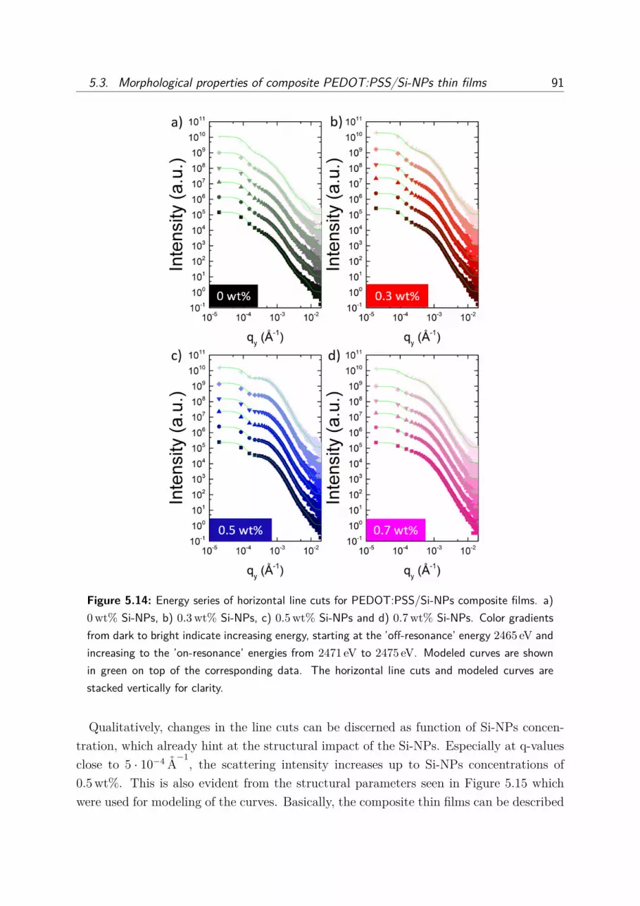
5.3. Morphological properties of composite PEDOT:PSS/Si-NPs thin films 91
Figure 5.14: Energy series of horizontal line cuts for PEDOT:PSS/Si-NPs composite films. a)0 wt% Si-NPs, b) 0.3 wt% Si-NPs, c) 0.5 wt% Si-NPs and d) 0.7 wt% Si-NPs. Color gradientsfrom dark to bright indicate increasing energy, starting at the ’off-resonance’ energy 2465 eV andincreasing to the ’on-resonance’ energies from 2471 eV to 2475 eV. Modeled curves are shownin green on top of the corresponding data. The horizontal line cuts and modeled curves arestacked vertically for clarity.
Qualitatively, changes in the line cuts can be discerned as function of Si-NPs concen-tration, which already hint at the structural impact of the Si-NPs. Especially at q-valuesclose to 5 · 10−4 A−1, the scattering intensity increases up to Si-NPs concentrations of0.5 wt%. This is also evident from the structural parameters seen in Figure 5.15 whichwere used for modeling of the curves. Basically, the composite thin films can be described
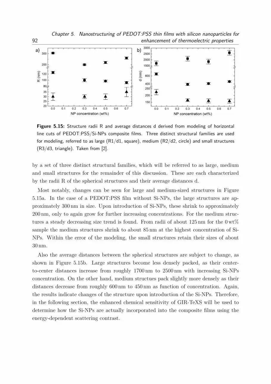
92Chapter 5. Nanostructuring of PEDOT:PSS thin films with silicon nanoparticles for
enhancement of thermoelectric properties
Figure 5.15: Structure radii R and average distances d derived from modeling of horizontalline cuts of PEDOT:PSS/Si-NPs composite films. Three distinct structural families are usedfor modeling, referred to as large (R1/d1, square), medium (R2/d2, circle) and small structures(R3/d3, triangle). Taken from [2].
by a set of three distinct structural families, which will be referred to as large, mediumand small structures for the remainder of this discussion. These are each characterizedby the radii R of the spherical structures and their average distances d.
Most notably, changes can be seen for large and medium-sized structures in Figure5.15a. In the case of a PEDOT:PSS film without Si-NPs, the large structures are ap-proximately 300 nm in size. Upon introduction of Si-NPs, these shrink to approximately200 nm, only to again grow for further increasing concentrations. For the medium struc-tures a steady decreasing size trend is found. From radii of about 125 nm for the 0 wt%sample the medium structures shrink to about 85 nm at the highest concentration of Si-NPs. Within the error of the modeling, the small structures retain their sizes of about30 nm.
Also the average distances between the spherical structures are subject to change, asshown in Figure 5.15b. Large structures become less densely packed, as their center-to-center distances increase from roughly 1700 nm to 2500 nm with increasing Si-NPsconcentration. On the other hand, medium structues pack slightly more densely as theirdistances decrease from roughly 600 nm to 450 nm as function of concentration. Again,the results indicate changes of the structure upon introduction of the Si-NPs. Therefore,in the following section, the enhanced chemical sensitivity of GIR-TeXS will be used todetermine how the Si-NPs are actually incorporated into the composite films using theenergy-dependent scattering contrast.

5.3. Morphological properties of composite PEDOT:PSS/Si-NPs thin films 93
Scattering contrast: deduction of composition
Through measurement of the 2D GISAXS patterns at energies close to the sulfur K-edge, a strong influence of the non-linearities of the optical properties on the observedscattering intensities can be achieved. Specifically, PEDOT shows such a response in the’on-resonance’ energy range from 2471 eV to 2475 eV, as seen in Figure 5.13.
The scattering contrast can be calculated according to Equation 2.31. Therein, thecontrast at the interface between two dissimilar materials is taken into account as anaverage δ1/β1 and δ2/β2, respectively. For the case of the ternary PEDOT:PSS/Si-NPscomposite films, this yields two possibilities for a general morphology. In the first case, itis assumed that Si-NPs are quantitatively dispersed within PEDOT-rich domains, whereasthe latter are themselves dispersed in a PSS-rich matrix. In the second case, the Si-NPsare fully dispersed in the PSS-rich matrix, which contains PEDOT-rich domains free ofnanoparticles. Both cases are schematically shown in Figure 5.16, and referred to asModel 1 and Model 2, respectively.
For the calculation of the scattering contrast ∆n21,2as function of both energy and Si-
NPs, the volume fraction vSi of the latter within the PEDOT-rich domains for Model1 and within the PSS-matrix for Model 2 is taken into account. In turn, this can becalculated with the knowledge of the average size of the Si-NPs of roughly 30 nm. Thus,the scattering contrasts ∆n2
1,2 for both models can be computed according to Equations5.1 and 5.2, respectively.
∆n21 = (δPSS − ((1− vSi)δPEDOT + vSiδSi))2+(βPSS − ((1− vSi)βPEDOT + vSiβSi))2
(5.1)
∆n22 = (((1− vSi)δPSS + vSiδSi)− δPEDOT )2+(((1− vSi)βPSS + vSiβSi)− βPEDOT ))2
(5.2)
Figure 5.16 summarizes the evolution of the energy-dependent scattering contrast asfunction of Si-NPs concentration for both models discussed above. It can be seen thatthe scattering contrast increases strongly with increasing introduction of nanoparticles,which is also independent of the assumed model. Considering Equations 5.1 and 5.2, thissimply originates from the increasing volume fraction of Si-NPs in the PEDOT-rich grainsand the PSS-rich matrix, respectively. However, a clear distinction can be made betweenthe two models in the ’on-resonance’ regime. While for Model 1 a local minimum of thescattering contrast is observed, the opposite is true for Model 2.
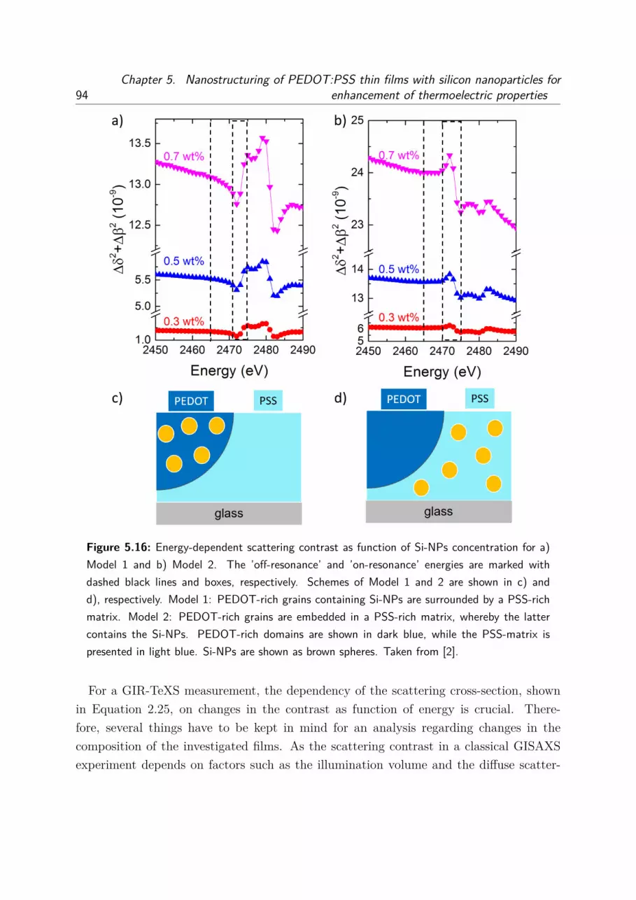
94Chapter 5. Nanostructuring of PEDOT:PSS thin films with silicon nanoparticles for
enhancement of thermoelectric properties
Figure 5.16: Energy-dependent scattering contrast as function of Si-NPs concentration for a)Model 1 and b) Model 2. The ’off-resonance’ and ’on-resonance’ energies are marked withdashed black lines and boxes, respectively. Schemes of Model 1 and 2 are shown in c) andd), respectively. Model 1: PEDOT-rich grains containing Si-NPs are surrounded by a PSS-richmatrix. Model 2: PEDOT-rich grains are embedded in a PSS-rich matrix, whereby the lattercontains the Si-NPs. PEDOT-rich domains are shown in dark blue, while the PSS-matrix ispresented in light blue. Si-NPs are shown as brown spheres. Taken from [2].
For a GIR-TeXS measurement, the dependency of the scattering cross-section, shownin Equation 2.25, on changes in the contrast as function of energy is crucial. There-fore, several things have to be kept in mind for an analysis regarding changes in thecomposition of the investigated films. As the scattering contrast in a classical GISAXSexperiment depends on factors such as the illumination volume and the diffuse scatter-

5.3. Morphological properties of composite PEDOT:PSS/Si-NPs thin films 95
ing factor Pdiff , the experiment itself and the subsequent analysis of the data has to beperformed accordingly.
In order to keep the illumination volume constant, one needs to make sure that thearea of the sample over which the beam is scanned possesses a homogeneous thickness,which is the case here. The four-crystal monochromator beamline at BESSY II allows forthe variation of the beam energy, while keeping the alignment of the beam with respectto the sample intact. Thus, no changes in the incident angle are observed, keeping theilluminated sample volume constant. All 2D GISAXS patterns are also normalized by theincident beam intensity, in order to exclude variations of the scattering intensity.
The influence of differences in scattering intensity due to scattering objects of certainshapes, sizes and spatial distributions is excluded in the modeling. It should be stressedthat for one energy series of a single sample, structural parameters had to be found whichcan be used for modeling of each curve within the series. The parameters listed in Figure5.15 fulfill this condition.
A discussion of the observed scattering intensities is therefore enabled. Figure 5.17compiles the scattering intensities from the modeling sorted by the three structural fami-lies which were considered. Therein, the intensities are shown as both function of energyand Si-NPs concentration.
Figure 5.17: Scattering intensities for a) large, b) medium and c) small structures included in themodeling of the horizontal line cuts, as function of energy. Colored data points represent 0 wt%(black), 0.3 wt% (red), 0.5 wt% (blue) and 0.7 wt% (magenta) Si-NPs in the composite films.All intensities are normalized for fluctuations in the incident beam intensity. Taken from [2].

96Chapter 5. Nanostructuring of PEDOT:PSS thin films with silicon nanoparticles for
enhancement of thermoelectric propertiesThe scattering intensity for large structures, shown in Figure 5.17a, appears to increase
with increasing amount of Si-NPs. When referring back to the scattering contrasts inFigure 5.16, this indicates increasing incorporation of Si-NPs into the film. Moreover, thepresence of a local minimum of the intensity at 2473 eV fits well to the proposed Model1, in which the Si-NPs are incorporated in PEDOT-rich grains.
A similar trend is also seen for the medium structures in Figure 5.17b. Also here thescattering intensity increases as more Si-NPs are added to the composite film. The localminimum observed at 2473 eV suggests inclusion of the nanoparticles into the PEDOT-richgrains, rather than the PSS-rich matrix.
Lastly, for the small structures neither a systematic increase in the intensity as functionof Si-NPs, nor a consistent local minimum/maximum at 2473 eV can be seen. An absenceof Si-NPs both within the PEDOT-rich grains and the PSS-rich matrix is suggested. Atleast for the former case, this is in line with the constant sizes of the small structures asfunction of Si-NPs observed in Figure 5.15a.
Morphological model and morphology-function relationship
From the structural and compositional information obtained from the GIR-TeXS mea-surement, it is possible to draw a morphological scheme seen in Figure 5.18. It containsboth the information on the spherical shape of PEDOT-rich domains, their average sizesand additionally their arrangement. More importantly however, the comparison of thescattering intensities in Figure 5.17 with the scattering contrast evolutions for the twopossible suggested models in Figure 5.16 reveals changes in the composition. As pointedout above, an overall increase of the scattering intensity for large and medium structures,as well as the local minimum at ’on-resonance’ energies is found. This suggests incor-poration of Si-NPs in PEDOT-rich grains, which becomes more prominent the more theSi-NPs concentration is increased.
Returning to the initial discussion of the thermoelectric properties of PEDOT:PSS/Si-NPs composite films and how they change as function of nanoparticle concentration,implications of the structure can be expected. These will be discussed in the following.Specifically, a correlation between the changes in the electrical and thermal conductivityand the modifications of the structure is found.
Figure 5.19 attempts at highlighting a correlation between the specific thermal resis-tance κ−1 (the inverse of the thermal conductivity) and the large structures, as well as theelectrical conductivity and the medium structures. As discussed in Section 5.2.2, the ther-mal conductivity changes non-linearly as function of Si-NPs concentration. The specificthermal resistance κ−1 in Figure 5.19a amounts to 0.98 KmW−1 for the pure PEDOT:PSS

5.3. Morphological properties of composite PEDOT:PSS/Si-NPs thin films 97
film. It decreases in an unfavorable way to values of 0.73 KmW−1 for 0.3 wr% Si-NPsonly to increase again. At the highest concentration of 0.7 wt%, a value of 1.03 KmW−1
slightly larger than that of the reference is reached. This implies a two-fold effect of thepresence of nanoparticles on the specific thermal resistance of the film. Firstly, as foundout in the compositional analysis using GIR-TeXS, an increasing incorporation of Si-NPsinto PEDOT-rich domains could be responsible for the increase in the specific thermalresistance. The inner structure of the latter could be disturbed by the Si-NPs, leadingto less efficient propagation of phonons and thus to larger values for κ−1. The initialdecrease of the latter, is easily understood when considering the single-crystalline natureof the Si-NPs. [34] At low concentrations, the improved phonon transport within the Si-NPs could possibly overcompensate the loss of short-range order within the PEDOT-richgrains, which is why κ−1 decreases. Secondly, increasing sizes of the structures seem tofavor phonon scattering, as a correlation between the sizes of the large structures and κ−1
can be seen.
Figure 5.18: Morphological model of PEDOT:PSS/Si-NPs composite films for different nanopar-ticle concentrations, as deduced from GIR-TeXS measurements and subsequent modeling. Thespherical PEDOT-rich grains are shown in blue, which themselves are embedded in a PSS-richmatrix, shown in light blue. Analysis of the scattering intensities and comparison to the scatter-ing contrast reveals validity of Model 1. Si-NPs are incorporated in large and medium structures,while small ones retain their purity. Additionally, Si-NPs are more efficiently included the higherthe nominal concentration becomes. Taken from [2].
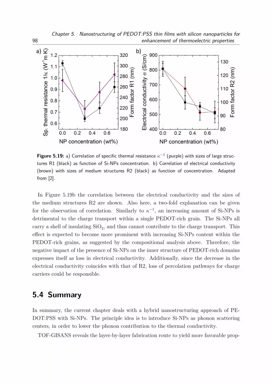
98Chapter 5. Nanostructuring of PEDOT:PSS thin films with silicon nanoparticles for
enhancement of thermoelectric properties
Figure 5.19: a) Correlation of specific thermal resistance κ−1 (purple) with sizes of large struc-tures R1 (black) as function of Si-NPs concentration. b) Correlation of electrical conductivity(brown) with sizes of medium structures R2 (black) as function of concentration. Adaptedfrom [2].
In Figure 5.19b the correlation between the electrical conductivity and the sizes ofthe medium structures R2 are shown. Also here, a two-fold explanation can be givenfor the observation of correlation. Similarly to κ−1, an increasing amount of Si-NPs isdetrimental to the charge transport within a single PEDOT-rich grain. The Si-NPs allcarry a shell of insulating SiO2, and thus cannot contribute to the charge transport. Thiseffect is expected to become more prominent with increasing Si-NPs content within thePEDOT-rich grains, as suggested by the compositional analysis above. Therefore, thenegative impact of the presence of Si-NPs on the inner structure of PEDOT-rich domainsexpresses itself as loss in electrical conductivity. Additionally, since the decrease in theelectrical conductivity coincides with that of R2, loss of percolation pathways for chargecarriers could be responsible.
5.4 Summary
In summary, the current chapter deals with a hybrid nanostructuring approach of PE-DOT:PSS with Si-NPs. The principle idea is to introduce Si-NPs as phonon scatteringcenters, in order to lower the phonon contribution to the thermal conductivity.
TOF-GISANS reveals the layer-by-layer fabrication route to yield more favorable prop-

5.4. Summary 99
erties of PEDOT:PSS/Si-NPs composite films as compared to the ones prepared in amixing approach, especially with respect to sizes of domains as well as the degree ofSi-NPs inclusion in the film.
Composite films prepared in a layer-by-layer approach with different concentrations ofSi-NPs are then investigated regarding their thermoelectric properties. The improvementof the power factor is ascribed to an increase in the Seebeck coefficient for concentra-tions up to 0.5 wt%. However, the electrical conductivity decreases simultaneously toapproximately 500 S/cm. Thus, optimal power factors of 27.6 µWK−2m−1 are achieved ata Si-NPs concentration of 0.5 wt%.
IRT is used in order to determine changes in the thermal conductivity as function of Si-NPs concentration. It is a contact-free method, which allows for the measurement of thein-plane thermal conductivity of the composite films, without the influence of a substrate.Free-standing PEDOT:PSS/Si-NPs films are prepared and suspended on steel substrateswith small cavities, on top of which the film is actually free-standing. The presence ofSi-NPs modifies the thermal conductivity non-linearly. Still, an overall improvement ofthe figure of merit ZT of a factor of 1.5 is found for the 0.5 wt% sample.
GIR-TeXS at the sulfur K-edge is used to elucidate the structural properties of thecomposite films as function of Si-NPs. Therein, the fact that both PEDOT and PSScontain sulfur but in different atomic configurations yields a different optical response foreach component close to the sulfur K-edge, as seen form the NEXAFS measurements.From the optical properties (namely δ and β), the energy-dependent scattering contrastis calculated. Two structural models are proposed, one in which Si-NPs are completelydispersed in PEDOT-rich grains, and a second one in which the Si-NPs are solely dispersedin the PSS-rich matrix. Horizontal line cuts of the 2D GISAXS patterns are modeled withthree distinct structural families, namely large, medium and small spherical structures.Modeling yields structural parameters which can be used to model all horizontal line cutswithin a single energy series. Since the scattering contrast changes with the incidentbeam energy, the same is expected for the scattering intensity off the different structures.Analysis of the intensity as function of energy and Si-NPs concentration, suggests validityof Model 1. Si-NPs are increasingly incorporated in large and medium PEDOT-richgrains, while the small ones retain their purity.
A morphological model is suggested, in addition to a morphology-function relationship.Therein, the thermal conductivity appears to be influenced by changes in the sizes of thelarge structures, while the electrical conductivity is mostly governed by changes in thesizes of medium structures. Changes in both thermoelectric quantities can additionallybe explained by the increasing incorporation of Si-NPs into these domains.


6 Dedoping of PEDOT:PSS withinorganic salts for optimization ofthermoelectric power factors
Large parts of this chapter have been published in the article: Facile Optimization ofThermoelectric Properties in PEDOT:PSS Thin Films through Acido-Base and RedoxDedoping Using Readily Available Salts (N. Saxena et al., ACS Appl. Energy Mater.,1, 336-342, 2018, DOI: 10.1021/acsaem.7b00334). [3] Parts of this chapter are based onthe bachelor’s thesis of Josef Keilhofer, [50] with initial studies having been performed byAnjani Kumar Maurya in the framework of his master’s thesis. [51]
Primary doping is a term which describes the introduction of charge carriers into con-jugated polymer chains by a doping process, as discussed in Section 2.2.1. In the case ofPEDOT as conjugated polythiophene, charges are introduced during the polymerizationprocess and subsequently stabilized in an electrostatically. In the case of e.g. PEDOT:Tos,the stabilization is mediated by negatively charged toluenesulfonate, or tosylate (Tos)ions. The electrical conductivities typically achieved for these types of films are amongthe highest measured for conducting polymer systems, with record values to date reachingup to 5400 S/cm. Gueye et al. used a structural variant of the tosylate anion and addedit to the polymerization mixture, in order to achieve these high conductivities. [52]
In the case of PEDOT:PSS, the negatively charged polyanion PSS is responsible forstabilization of charges on the PEDOT chains. This allows for dispersion of the otherwisecompletely insoluble PEDOT in aqueous solution, and thereby enables solution-processingtechniques, such as spin- or spray-coating for thin film fabrication. Through variation ofthe PEDOT-to-PSS ratio during production, the properties of the dispersion, and thusof the final films can be manipulated. For different applications, specific formulations ofPEDOT:PSS are used, which mostly vary in the ratio of PEDOT-to-PSS and thereforein their electrical and/or optical properties when fabricated as thin film, as summarizedin the review of Shi et al. [53] One of these formulations is commonly referred to asClevios PH1000, with a mass ratio of PEDOT-to-PSS of 1:2.5. In their study, Park et al.
101
102Chapter 6. Dedoping of PEDOT:PSS with inorganic salts for optimization of
thermoelectric power factorsdemonstrated the impact of PEDOT-to-PSS ratio on the electrical conductivity, with theaforementioned ratio yielding the highest conductivity values. [13] These findings can becombined with the investigation of Massonnet et al., who performed UV-Vis spectroscopyon thin films of the PH1000 formulation, and found strong optical absorption in the far-infrared region of the spectrum. The authors assigned this to the presence of bipolarons,which act as majority charge carriers. The occurrence of bipolarons is synonymous witha high charge carrier density, which is in line with the potentially very high electricalconductivities that can be achieved in thin films of PH1000.
While these properties make PEDOT:PSS a viable choice for application as e.g. trans-parent electrode in organic solar cells or light-emitting diodes, there are also drawbacks.As discussed in Section 2.1.2, a high charge carrier concentration is typically associatedwith low Seebeck coefficients. Due to quantities such as the figure of merit ZT or thepower factor showing a square dependence on the Seebeck coefficient, this fact impedesthe obtainment of high efficiency devices. Thus, researchers have attempted to overcomethis problem by modifying the charge carrier concentration of PEDOT:PSS mostly afterfilm fabrication. Bubnova et al. used vapors tetrakis(dimethylamino) ethylene (TDAE)vapors, and were able to modify oxidation levels in PEDOT:Tos as they showed usingXPS. This way they could achieve power factors of over 300 µWK−2m−1, which for themost part stems from the improvement of the Seebeck coefficient. [54] As an alternativeapproach, Fan et al. performed post-treatment steps of PEDOT:PSS films with sulfuricacid and sodium hydroxide. Through analysis of the films with various spectroscopic tech-niques, the authors deduced that reduction of the charge carrier concentration was causedby the basic properties of sodium hydroxide, and therefore allowed for improvement ofthe Seebeck coefficient. [55] Massonnet et al. used various reducing agents, such as hy-drazine, NaBH4, Na2SO3 or the above-mentioned TDAE. [56] These were chosen on thebasis of their different redox potentials, expected to yield increased Seebeck coefficientsafter post-treatment of PEDOT:PSS films. With UV- Vis spectroscopy, the authors ob-served changes in the absorption behavior upon dedoping. The large absorption in thefar-infrared range of the spectrum assigned to the presence of bipolarons steadily shiftstowards lower wavelengths when the reducing agents are applied to the polymer films.Strong reducing agents yielded strong absorption festures in the visible region, and wereassigned to the presence of neutral states.
Similarly, this study attempts to investigate the influence of dedoping in PEDOT:PSSfilms more closely in terms of changes in the thermoelectric properties caused by changesin charge carrier concentration. Dedopants are chosen according to their acido-basic orredox properties, and compared regarding their dedoping efficiency. Various spectroscopic

6.1. Thermoelectric characterization of dedoped PEDOT:PSS thin films 103
techniques are used to analyze changes in the electronic structure, composition and con-formation of the films.
6.1 Thermoelectric characterization of dedopedPEDOT:PSS thin films
In the following section, PEDOT:PSS thin films will be dedoped using inorganic salts,which exhibit either acido-basic or redox properties. NaHCO3 exhibits acido-basic prop-erties, while Na2SO3 and NaBH4 show redox behavior. Dedoping is done in a facile ap-proach, in which aqueous solutions of the inorganic salts are mixed in different amountsinto PEDOT:PSS solutions prior to film fabrication. EG post-treatment is performedon all samples in order to increase the electrical conductivity through secondary dopingto levels at which the influence of the charge carrier concentration can be discerned. Adetailed description of the experimental procedure is given in Section 4.2.2.
The properties of the samples are discussed in terms of changes in the Seebeck coef-ficient, electrical conductivity and power factor as function of dedopant concentration.Dedoping with the redox-active salts is also analyzed with respect to the absolute num-ber of reducing equivalents, in an effort to understand if the choice of redox-active saltinfluences the outcome.
6.1.1 Acido-basic dedoping with sodium hydrogencarbonate
Firstly, NaHCO3 is employed as inorganic salt with purely acido-basic properties. Itdecomposes into carbon dioxide, sodium and hydroxyl ions, as seen in Equation 6.1.
NaHCO3 −−→ Na+ + OH− + CO2 (6.1)
In Figure 6.1, the three important thermoelectric quantities, namely Seebeck coefficient(green), electrical conductivity (brown) and power factor (blue) are shown as functionof NaHCO3 concentration. An increase of the Seebeck coefficient from 24.7µV/K forthe sample without NaHCO3 to a maximum value of 54.8µV/K at a concentration of70 mM is observed, which levels off for higher concentrations. Simultaneously, a strongdecrease in the electrical conductivity from 875 S/cm to approximately 115 S/cm is found,after reaching a maximum value close to 1000 S/cm for low concentrations. Since allsamples were treated with EG, there is an indication that the negative effect on the

104Chapter 6. Dedoping of PEDOT:PSS with inorganic salts for optimization of
thermoelectric power factors
Figure 6.1: Seebeck coefficient (green diamonds), electrical conductivity (brown hexagons) andpower factor (blue triangles) of PEDOT:PSS films dedoped with different concentrations ofNaHCO3. Dashed lines in the respective colors serve as guides to the eye. Taken from [3].
electrical conductivity comes from changes in the charge carrier concentration, which isalso supported by the increase in the Seebeck coefficient. Nevertheless, the thermoelectricquantities were altered in such a way that the power factor (blue data points) shows amaximum value of approximately 100 µWK−2m−1 at a concentration of 24 mM, with thereference value being 53 µWK−2m−1. Due to the square dependence of the power factoron the Seebeck coefficient, a certain drop in the electrical conductivity can be accepted,since the Seebeck coefficient increases accordingly and is therefore mainly responsible forthe improvement. Further increase of the dedopant concentration leads to even higherSeebeck coefficients but to drastically lower electrical conductivities which result in anoverall decrease of power factors in this concentration range. Another noteworthy factis that the maximum NaHCO3 concentration used in this study is significantly lowerthan for the other salts. This is owed to the fact that the inorganic salts not only alterthe electronic structure of PEDOT, but also modify the electrostatic interaction betweenPEDOT and PSS. As PEDOT by itself is completely insoluble, a disturbance in thecoordination of PSS onto PEDOT chains leads to inhomogeneous film formation, whichcan be observed in the optical microscopy images in Figure 6.2.While both the pristine,EG-treated PEDOT:PSS film and the one with the optimal concentration of dedopantappear homogeneous, the optical micrograph of the film dedoped with very high NaHCO3
concentrations of 193 mM appear much darker. A strong increase in the viscosity of thepolymer solution is observed, when high concentrations of NaHCO3 are added, which

6.1. Thermoelectric characterization of dedoped PEDOT:PSS thin films 105
Figure 6.2: Exemplary optical micrographs of PEDOT:PSS films dedoped with NaHCO3 indifferent concentrations: a) 0 mM, b) 24 mM and c) 193 mM. Taken from [3].
in turn makes the flinging-off of material less efficient. Also, measuring the Seebeckcoefficient becomes exceedingly difficult if no closed film is present on the substrate,which is why the maximum concentration of NaHCO3 was 82 mM.
6.1.2 Redox dedoping with sodium sulfite and sodium borohydride
In a complementary approach, dedoping of PEDOT:PSS thin films was also attemptedwith the inorganic salts Na2SO3 and NaBH4 since they possess redox-properties, dueto them being able to release electrons and hydride ions (negatively charged hydrogenatoms), respectively. For both salts, the decomposition reactions in aqueous solution areshown in Equations 6.3 and 6.2, respectively.
Na2SO3 + H2O −−→ 2 Na+ + SO42− + 2 H+ + 2 e− (6.2)
2 NaBH4 −−→ 2 Na+ + B2H6 + 2 H− (6.3)
Redox-dedoping with sodium sulfite (Na2SO3)
As shown in Equation 6.2, sodium sulfite decomposes into sulfate anions and protonsunder release of two equivalents of electrons per equivalent of salt, whereas the formerare expected to interact with PEDOT in a charge-neutralizing fashion. Figure 6.3 sum-marizes the impact of dedoping PEDOT:PSS as function of Na2SO3 concentration. Aswith dedoping using NaHCO3, also here an increase of Seebeck coefficient to 69.0µV/K

106Chapter 6. Dedoping of PEDOT:PSS with inorganic salts for optimization of
thermoelectric power factors
Figure 6.3: Seebeck coefficient (green diamonds), electrical conductivity (brown hexagons) andpower factor (blue triangles) of PEDOT:PSS films dedoped with different concentrations ofNa2SO3. Dashed lines in the respective colors serve as guides to the eye. Taken from [3].
from 24.4µV/K is observed, which levels off for high concentrations. Notably, the max-imum Seebeck coefficient for dedoping with Na2SO3 is higher than in the other cases,which will be discussed below. Again, the rise in Seebeck coefficient is complemented bya drastic decrease in electrical conductivity, with the reference value being 1050 S/cm andfalling down to 36 S/cm for high concentrations. As discussed before, due to the squaredependence of the power factor on the Seebeck coefficient, again an optimum value of90 µWK−2m−1 of the former is found at concentrations of 12 mM Na2SO3, compared tothe reference value of approximately 60µWK−2m−1. For high concentrations, the powerfactor drops to 20µWK−2m−1, due to the loss in electrical conductivity.
Redox-dedoping with sodium borohydride (NaBH4)
NaBH4 decomposes in aqueous solution into the stable diborane (B2H6) and sodium ionsunder the release of negatively charged hydride anions (H–), which are responsible for thereductive properties of the salt. This is highlighted in Equation 6.3. Figure 6.4 shows theevolution of thermoelectric properties as function of NaBH4 concentration. As previouslyseen, the addition of dedopant yields changes in the Seebeck coefficient, which increasesfrom 23.0 µV/K for the reference to 58.0µV/K for the highest concentration of 160 mMNaBH4. Consequently, the electrical conductivity drops from 940 S/cm for the samplewithout dedopant, to 49 S/cm for the highest concentration of 160 mM. In addition,

6.1. Thermoelectric characterization of dedoped PEDOT:PSS thin films 107
Figure 6.4: Seebeck coefficient (green diamonds), electrical conductivity (brown hexagons) andpower factor (blue triangles) of PEDOT:PSS films dedoped with NaBH4. Dashed lines in therespective colors serve as guides to the eye. Taken from [3].
the latter quantity shows a only a very slight decrease for concentrations up to 24 mM.Interestingly, this is also the concentration at which the maximum value for the powerfactor of 96µWK−2m−1 is found, giving an improvement of factor two compared to thereference. As before, a large drop down to approximately 20 µWK−2m−1 is observed forlarge concentrations.
Comparison of redox dedopants
In the discussion above, changes among the different redox dedopants regarding the mag-nitudes of the different thermoelectric properties are apparent. The question whether thisstems from differences in redox potential or not, is reasonable. Therefore, in Figure 6.5,the three previously discussed quantities are discussed in terms of the absolute numberof reducing equivalents. These were calculated based on the reaction schemes given inEquations 6.2 and 6.3. From these, it can be concluded that per mole of Na2SO3 twomoles of electrons are released, while per mole of NaBH4 only one mole of H– is releasedinto the solution. The employed salt concentrations were thusly modified with a factor oftwo in the case of Na2SO3 and with a factor of one in the case of NaBH4, in order to giveshow the thermoelectric quantities as function of a ’normalized’ concentration.
For both the Seebeck coefficient and electrical conductivity, a very good agreement be-tween the two redox-active salts is found as function of reducing equivalent concentration.

108Chapter 6. Dedoping of PEDOT:PSS with inorganic salts for optimization of
thermoelectric power factors
Figure 6.5: a) Seebeck coefficient, b) electrical conductivity and c) power factor for PEDOT:PSSfilms dedoped with Na2SO3 (solid symbols) and NaBH4 (hollow symbols) as function of absolutenumber of reducing equivalents. These were calculated based on the decomposition reactionsgiven in Equations 6.2 and 6.3. Dashed, colored lines serve as guides to the eye. Taken from [3].
The Seebeck coefficient increases steadily and reaches saturation for high concentrationsat values close to 70µV/K. Consequently, the electrical conductivity decreases drastically,
6.2. Spectroscopic characterization 109
since already reducing equivalent concentrations of approximately 70 mM reduce the elec-trical conductivity below 200 S/cm. Naturally, by combining the different trends for theSeebeck coefficient and electrical conductivity, an overall optimum of the power factor isexpected, which is also seen in Figure 6.5c. It can be observed that only minor increasesof the Seebeck coefficient of up to approximately 40 µV/K are needed to achieve the max-imum power factor, since this goes along with reasonably high electrical conductivities ofapproximately 500 S/cm.
The good agreement of the parameters for the two salts is a clear hint that the individualproperties of the redox-active salts have less of an impact than the absolute amount ofreducing equivalents in solution which can interact with the positive charge carriers onthe PEDOT chains.
In summary, inorganic salts with acido-basic and redox-active properties can be used inorder to tune the thermoelectric properties of PEDOT:PSS thin films. In order to under-stand the source of these effects the dedoped films are analyzed using various spectroscopictechniques in an effort to understand whether the intended modification of charge carrierconcentration is solely responsible or not.
6.2 Spectroscopic characterization
6.2.1 Analysis of electronic structure with UV-Vis spectroscopy
UV-Vis spectroscopy is a non-destructive method, with which the electronic structureof PEDOT:PSS can be analyzed. Massonnet et al. used this technique in their owndedoping study to not only deduce the electronic structure of pristine PEDOT:PSS, butalso to monitor changes upon addition of dedopants. In the former case, absorptionprimarily takes place in the infrared region of the spectrum, due to the high concentrationof bipolarons as charge carriers, which are easily excited by low-energy light. [56] Uponaddition of dedopant, they found a steady decrease of absorption in this region, whilesimultaneously increased absorption in the near-infrared and visible range was found.The authors assigned this to a transition from bipolarons to polarons and neutral specieswith increasing reducing power of dedoping agent.
In this study, UV-Vis spectroscopy is similarly used to determine changes in the elec-tronic structure of PEDOT:PSS. Specifically, we want to monitor changes in the chargecarrier distribution and link them to changes in the thermoelectric properties.
Figure 6.6 shows the evolution of UV-Vis absorption spectra as function of concen-tration for all three previously discussed dedopants. Normalization of the spectra at

110Chapter 6. Dedoping of PEDOT:PSS with inorganic salts for optimization of
thermoelectric power factors
Figure 6.6: Normalized absorption coefficients of PEDOT:PSS films dedoped with a) NaHCO3,b) Na2SO3 and c) NaBH4. The curves are stacked along the y-axis for clarity, with the con-centration of the respective dedopant increasing from bottom to top. Normalization to theabsorption coefficient at 400 nm was performed for all curves in order to highlight the changesupon dedoping. In each graph, the bottom-most graph (black) represents PEDOT:PSS treatedwith EG but not with dedopant. Taken from [3].
wavelengths of 400 nm was performed in order to highlight changes with increasing con-centration of each dedopant, but also possible differences between each dedopant. Eachgraph contains the reference curve for PEDOT:PSS only post-treated with EG in black,while the color gradient transitioning to light green is supposed to link the increasingdedopant concentration to the increasing Seebeck coefficient for all cases.
As seen by Massonnet et al., due to bipolarons being the majority charge carrier type,pristine PEDOT:PSS shows increased absorption towards longer wavelengths. Visiblewavelenghts are absorbed to lesser extent, which is why thin films of PEDOT:PSS typicallyappear semi-transparent. Upon dedoping with NaHCO3, the broad absorption shoulderat high wavelengths gradually transforms into a broad peak. This can be assigned to thegradual transformation of bipolarons into polarons. For concentrations exceeding 24 mM,another feature arises at around 650 nm. This is typically assigned to the presence ofneutral states of PEDOT. The increase in absorption corresponding to polaron states onthe one hand, and also the increased concentration of neutral states fits well with therise in Seebeck coefficient, since an inverse relation of Seebeck coefficient and number ofcharge carriers is expected.
A similar general trend is also seen for dedoping with the redox-active salts Na2SO3 andNaBH4, which also exhibit increase in polaron concentration with lower amounts of salt,and additional neutral states appearing, which can be deduced from the presence of ab-

6.2. Spectroscopic characterization 111
sorption features around 650 nm. For Na2SO3, these appear for concentrations exceeding12 mM, while for NaBH4, they appear at concentrations higher than 24 mM. Interestingly,in all cases the concentration of dedopant at which absorption features related to neutralspecies arise, also mark the point at which the optimum power factor is already exceeded.A possible conclusion which can be drawn from this finding is that the presence of po-larons is favorable, while neutral states impede the electrical conductivity too much. Eventhe maximum Seebeck coefficients that can be achieved with the highest dedoping con-centrations cannot compensate this in terms of the power factor. Additionally, despite theinorganic salts presumably reacting with PEDOT chains in different ways due to NaHCO3
possessing acido-basic and Na2SO3 and NaBH4 having redox-active properties, dedopingappears to have very similar effects on the thermoelectric properties of PEDOT:PSS thinfilms.
6.2.2 Compositional analysis with x-ray photoelectron spectroscopy
In order to understand the effects of the different dedopants more, in the following sectionXPS is employed. It not only allows to determine the composition of dedoped films butalso if the average oxidation levels of sulfur in PEDOT change, which can in principle belinked to changes in charge carrier concentration. In this specific case, measurements wereperformed at the S2p-absorption edge of sulfur. Sulfur is present in both PEDOT and PSS,albeit with different chemical environments. Due to the sensitivity of XPS to differencesin chemical environments or chemical shift, these two different species of sulfur can bedistinguished by the binding energy of electrons in the 2p-orbitals. One is therefore ableto make statements about the chemical composition of the films, simply by analyzing peakareas. In addition, since the peak position is sensitive to the binding energy of electrons,it is therefore also subject to change during oxidation/reduction processes. Here, this factwill be used to make statements about the average oxidation levels of PEDOT. For thispurpose, PEDOT:PSS films were dedoped with the different inorganic salts in exemplaryconcentrations.
The reference measurement for PEDOT:PSS only post-treated with EG (black curve inFigure 6.7a), reveals a strong contribution of the PSS signal at higher binding energies,centered at around 168 eV. This can be easily understood when considering the natureof the chemical shift. The sulfur in PSS is bound to three oxygen atoms which stronglydecrease the electron density around it. Each individual core electron thus experiences ahigher electrostatic binding through the positive charge of the sulfur core, which manifestsitself as a shift towards higher binding energies in the XPS spectra. [55] The weak PEDOTsignal is found at comparatively lower binding energies of around 165 eV due to the binding

112Chapter 6. Dedoping of PEDOT:PSS with inorganic salts for optimization of
thermoelectric power factors
Figure 6.7: a) High resolution XPS S2p spectra of PEDOT:PSS dedoped with NaHCO3 inconcentrations of 5 mM, 24 mM and 71 mM, with PEDOT:PSS only post-treated with EG isshown as reference in black. Curves obtained from samples with increasing concentrations ofdedopant are stacked along the y-axis for clarity. b)-d) Deconvolutions of high resolution XPSspectra, for the dedoped samples with concentrations indicated as above. Spin-splitting of thesignal is accounted for in the fitting of the peaks with Gaussian-Lorentzian lineshapes. Adaptedfrom [3].
of the sulfur in the thiophene unit of the monomer. From the peak areas, conclusionsabout an excess of PSS can be made. However, it should be noted that the limitedinformation depth of XPS of approximately 8 nm limits this statement to the uppermostlayers of the film. This strong disbalance in peak area therefore corresponds to a thincapping layer of PSS which rests on top of the PEDOT:PSS film after post -treatmentwith EG.
An aspect that is also of interest for this discussion is tracking peak positions of thePEDOT contribution to the XPS spectra as function of dedopant concentration. This

6.2. Spectroscopic characterization 113
will give more insight into the reduction mechanism and possibly into differences amongthe different dedopants.
In Figure 6.7a no significant shift of the PEDOT signal towards lower binding energies,as one would expect from reduced thiophene sulfur, can be detected. This is supportedby closer investigation of the deconvolution spectra in Figure 6.7b-d. Mechanistically,this speaks for a decrease in charge carrier concentration solely due to neutralization ofprotons with the hydroxyl anions that form upon decomposition of NaHCO3 in aqueoussolution (see Equation 6.1). This finding is in good agreement with the work of Fan et al.,who used sodium hydroxide (NaOH) for post-treatment of PEDOT:PSS and similarly sawincreased optical absorption in the visible region of the spectrum, as well as changes in thePEDOT-to-PSS ratio but no shift of the PEDOT contribution in the XPS spectra. [55]
In the case of Na2SO3 dedoping, as seen in Figure 6.8a, a similar relative increase in thePEDOT contribution is seen, which most likely originates from a decrease in the relativeamount of PSS on the surface. The additional shoulder appearing at high binding energiesis most likely related to sulfur in the form of sulfate ions, which form after decompositionof Na2SO3 in aqueous solution (as can be seen in Equation 6.2). Since four oxygen atomsare bound to a single sulfur atom, the decreased electron density should increase thebinding energy for each individual electron compared to the sulfonate sulfur present inPSS. Additionally, a shift of the PEDOT contribution towards lower binding energiesis observed, as seen from the deconvolutions of the S2p signal in Figures 6.8b-d. Thisindicates a reduction in the average oxidation level of thiophene sulfur, and thereforecorresponds to a loss in charge carrier concentration in PEDOT chains. As opposed todedoping with NaHCO3, actual reduction of positive charge carriers within PEDOT chainstakes place with the help of electrons which are released from the salt upon decompositionin water.
Lastly, the XPS spectra after dedoping of PEDOT:PSS with NaBH4 are shown in Figure6.9. Also here, the removal of PSS is more efficient, which manifests itself as relativeincrease of the PEDOT-associated peaks. Notably, a strong shift of approximately 0.7 eVthose peaks towards lower binding energies are observed for high concentrations of NaBH4.The hydride ions (H–) which are released upon reaction of NaBH4 in aqueous solution,as seen in Equation 6.3, are responsible for the apparent reduction of thiophene sulfur.The indicated reduction of charge carrier concentration is in line with the observationin UV-Vis spectra of dedoped PEDOT:PSS films and also with the increase in Seebeckcoefficient. One thing which should be kept in mind is that NaBH4 not only possessespurely redox-active properties, but also acido-basic ones since the hydride anion can alsoact as a strong base. At the highest concentration of 91 mM, PEDOT:PSS solutions showpH values of approximately 12.7, while the pristine solutions exhibit pH values of 1.5.

114Chapter 6. Dedoping of PEDOT:PSS with inorganic salts for optimization of
thermoelectric power factorsStill, the acido-basic properties themselves cannot solely be responsible for the observedeffects, since the shift of the PEDOT peaks in the XPS spectra indicates actual reductionof the average oxidation level of the thiophene sulfur. This notion is supported by thePEDOT:PSS films dedoped with NaHCO3 showing no shift of the PEDOT-associatedpeaks in the XPS spectra.
As described above, XPS also allows for analysis of the composition, by simply calcu-lating ratios of peak areas. Here, an estimate of the PSS-to-PEDOT ratio is obtained bysumming the peak areas of the peaks associated to PSS and PEDOT, respectively and
Figure 6.8: a) High resolution XPS S2p spectra of PEDOT:PSS dedoped with Na2SO3 inconcentrations of 5 mM, 12 mM and 91 mM, with PEDOT:PSS only post-treated with EG isshown as reference in black. Curves obtained from samples with increasing concentrations ofdedopant are stacked along the y-axis for clarity. b)-d) Deconvolutions of high resolution XPSspectra, for the dedoped samples with concentrations indicated as above. Spin-splitting of thesignal is accounted for in the fitting of the peaks with Gaussian-Lorentzian lineshapes. Adaptedfrom [3].

6.2. Spectroscopic characterization 115
Figure 6.9: a) High resolution XPS S2p spectra of PEDOT:PSS dedoped with NaBH4 in con-centrations of 5 mM, 24 mM and 91 mM, with PEDOT:PSS only post-treated with EG is shownas reference in black. Curves obtained from samples with increasing concentrations of dedopantare stacked along the y-axis for clarity. b)-d) Deconvolutions of high resolution XPS spectra,for the dedoped samples with concentrations indicated as above. Spin-splitting of the signal isaccounted for in the fitting of the peaks with Gaussian-Lorentzian lineshapes. Adapted from [3].
calculating the ratio. The result for the different dedopants in exemplary concentrationsis shown in Figure 6.10. As can already be seen in the XPS spectra discussed previously,the PEDOT:PSS film without dedopant but after post-treatment with EG possesses acapping layer of PSS, which yields the high apparent PSS-to-PEDOT ratio. In all casesof dedoping, this ratio drastically reduces due to improved removal of PSS due to post-treatment and shows a monotonous decreasing trend. One exception is the PEDOT:PSSfilm dedoped with high concentrations of Na2SO3, for which the ratios slightly increasesagain. Remnants of sulfate formed after the decomposition of Na2SO3 might make the

116Chapter 6. Dedoping of PEDOT:PSS with inorganic salts for optimization of
thermoelectric power factors
Figure 6.10: Ratio of PSS to PEDOT extracted from peak areas in S2p XPS scans for selectedconcentrations of NaHCO3 (red), Na2SO3 (green) and NaBH4 (blue). Taken from [3].
determination of the PSS peak area inaccurate, and are therefore most likely responsiblefor this observation.
6.2.3 Conformational analysis with Raman spectroscopy
Raman spectroscopy is employed in this study to investigate changes in the conformationof polymer chains upon dedoping. In the case of polythiophenes, or more specificallyPEDOT, Raman spectroscopy enables the distinction between the two distinct states inwhich the monomer exists, namely the benzoid and quinoid forms of PEDOT, as seenin Figure 6.11 on the left and right respectively. The question is whether the dedopingprocess influences the structure of the EDOT monomers as compared to the referencesample, and if those changes can be linked to the observed drop in electrical conductivityfor all dedopants. Implications of the monomer structure on macroscopically measuredproperties are expected since both forms of the monomer favor different conformations ofthe chain. While the benzoid form of the monomer bonds to the next repeating unit of thepolymer chain via a single bond, in the quinoid form monomers are connected via doublebonds. In the former case rotation around the bond axis is energetically more favoredthan in the latter case. This causes differences in the conformation of the polymer chain,as a more coil-like conformation is taken on by the chain if the benzoid form is prevalent.If the quinoid form dominates, the opposite is the case, since the high energy barrier for

6.2. Spectroscopic characterization 117
Figure 6.11: Benzoid (left) and quinoid form (right) of EDOT, impacting polymer chain con-formation.
rotation causes the chains to adapt an extended-coil or linear conformation. This in turnis expected to be more favorable for charge transport due to better overlap of p-orbitalsand therefore greater spatial extent of the conjugated π-system.
For the acquisition of Raman spectra of dedoped PEDOT:PSS films, preliminary testswere performed regarding feasible intensities of the excitation laser, as well as suitableintegration times. Figure 6.12 shows spectra obtained at 2 mW laser power on the left and0.5 mW on the right for different integration times. Irrespective of laser power, additionalpeaks arise in the spectra after longer integration times, mostly located around 1500 cm−1,in addition to an increased background. Therefore, for all measurements discussed in thisstudy, spectra were acquired by scanning across the sample, in order to decrease the dwell-time of the excitation laser on each individual spot. This allowed for usage of higher laserpowers and additionally shorter integration times, without damaging the samples.
Figure 6.12: Raman spectra of an exemplary PEDOT:PSS film acquired at laser powers of2 mW (left) and 0.5 mW (left). Integration times of 0.1 s are represented in black spectra, whiletimes of 0.9 s are shown in red spectra. Taken from [3].
Raman spectroscopy was performed on PEDOT:PSS thin films prepared on glass sub-strates by irradiating macroscopic, representative sections of the films and measuring

118Chapter 6. Dedoping of PEDOT:PSS with inorganic salts for optimization of
thermoelectric power factorsRaman spectra at each illuminated spot. Figure 6.13a shows an optical micrograph ofan exemplary film overlayed with a Raman intensity map, which was obtained from themeasurement of the intensity of a prominent Raman band (located at 1435 cm−1) within
Figure 6.13: a) Overlay of an optical micrograph of an exemplary PEDOT:PSS film, with acorresponding 20 µm · 20 µm Raman intensity map. A correlation between particles visible in themicrograph and a very high Raman intensity is apparent. The strong signal typically originatesfrom a strongly fluorescent background. b) Raman intensity map corresponding to a), obtainedusing a band-pass filter around 1435.0(375) rel cm−1. c) Mask used for averaging multipleRaman spectra over the scanned area. Out of the 60 · 60 pixels, corresponding to 3600 spectra,only the yellow pixels are considered for averaging. Black ones were deemed unsuitable, due tofluorescence contributions to the signal. A Raman map was used for averaging of the spectra, ifmore than 3000 pixels in the mask were yellow. d) Green and blue spectra taken at the positionsindicated with the cross-hairs in b) after an integration time of 0.2 s. Noisy spectra were obtainedin both cases, however with a strong fluorescence signal in the green spectrum. The red curverepresents the average Raman spectrum after taking into account all pixels, exhibiting a largerbackground in the entire spectrum, while the signal-to-noise ratio is improved in the black curveafter ommitting the black pixels. Here, characteristic signals of PEDOT become visible due toaveraging of the noise. Taken from [3].

6.2. Spectroscopic characterization 119
the spectrum across a macroscopic area of 20 µm · 20µm. Upon closer investigation of theoverlay image, the correlation between impurities on the film surface and exceptionallystrong signals becomes apparent. The latter signals typically have strong contributionsfrom fluorescence. The Raman intensity maps are thus carefully analyzed regarding fluo-rescence signals, as highlighted by the blue and green cross-hairs in Figure 6.13b. Thesecorrespond to the blue and green spectra in Figure 6.13, which show large contributionsfrom fluorescence in the green spectrum that are absent in the blue spectrum. In order toavoid detriments to the data analysis, a mask is used (shown in Figure 6.13c) which ne-glects pixels in the Raman intensity map that show strong fluorescence contributions. Theneglected pixels are shown in black, while the ones used for averaging the Raman signalover more than 3000 pixels are highlighted in yellow. The improvement due to exclusionof fluorescence can be seen when comparing the red spectrum (averaged with fluorescencesignal) to the black spectrum (averaged under exclusion of fluorescence) in Figure 6.13d.Averaging under the exclusion of fluorescent pixels yields a better signal-to-noise ratio,with background levels reduced in general.
For discussion of the Raman spectra of dedoped PEDOT:PSS films, the same concen-trations as for the XPS measurements shown above were used. Figure 6.14 shows Ramanspectra obtained for the three dedopant salts, with the reference curve for a PEDOT:PSSfilm only post-treated with EG in black. The band positions for the latter match very wellwith the ones measured by Stavytska-Barba et al. [57] Upon dedoping, the central bandlocated at around 1420 cm−1 becomes narrower with increasing concentration of dedopant.More accurately, since the central band is asymmetric, with the lower wavenumber con-tribution decreasing in intensity, the dedoping makes the former appear narrower. Taking
Figure 6.14: Raman spectra of PEDOT:PSS dedoped with a) NaHCO3 in concentrations of5 mM, 24 mM and 71 mM, b) Na2SO3 in concentrations of 5 mM, 12 mM and 91 mM andc) NaBH4 in concentrations of 5 mM, 12 mM and 91 mM. Spectra are stacked on top of eachother for clarity. While the black spectra in each image represent PEDOT:PSS without dedopant,the color gradient from dark to light green indicates increasing concentration of the respectivededopant. Taken from [3].

120Chapter 6. Dedoping of PEDOT:PSS with inorganic salts for optimization of
thermoelectric power factorsthe analysis of Raman spectra performed by Nevrela et al. into consideration, this lowerwavenumber contribution can be assigned to the quinoid form of PEDOT. A decreaseof this contribution therefore indicates a decrease in relative amount of that form. Ad-ditionally, the shoulder located at 1499 cm−1 in the reference spectrum, becomes morepronounced and shifts to larger wavenumbers upon dedoping in all cases. This is againindicative of an increase in the relative amount of the benzoid form of PEDOT as func-tion of dedopant concentration. Both the decrease of the amount of quinoidal PEDOT,and the increase in benzoidal PEDOT are in line with the observed loss in electricalconductivity which was observed for increasing concentrations of dedopant, irrespectiveof the type of employed dedopant. As discussed above, this most likely correlates witha transition from a more extended-coil or linear conformation of PEDOT chains whenthe quinodal form is present, into a more coil-like conformation after dedoping, due toa strong increase in the amount of the benzoidal form. In conclusion, the macroscopicloss in electrical conductivity can be assigned to the combination of the transition from alinear or extended-coil conformation to a more coil-like conformation, and a decrease inthe number of charge carriers.
6.3 Summary
In summary, dedoping of PEDOT:PSS thin films with readily available inorganic saltspresents a facile and feasible way of optimizing thermoelectric properties. The improve-ment relies largely on the increase of Seebeck coefficients, while a simultaneous decrease inelectrical conductivity is observed. This can be tolerated, since the Seebeck coefficient ofhighly conducting PEDOT:PSS in the PH1000 formulation is typically very low and thusthe limiting factor. Notably, the Seebeck coefficients and power factors improve for alldedopants, irrespective of the latters’ chemical properties. NaHCO3 which decomposes inacido- basic reactions increases the Seebeck coefficient just as well as Na2SO3 and NaBH4
which exhibit redox-activity. When comparing the latter two salts, it was also foundthat the improvement depends less on the employed reducing agent and its properties(e.g. redox potential) and more on the absolute number of reducing equivalents whichare present in solution and able to interact with PEDOT. The maximum power factorsachieved in this study were 100 µWK−2m−1 upon dedoping with NaHCO3, 90 µWK−2m−1
with Na2SO3 and 95 µWK−2m−1 with NaBH4 at optimal concentrations.UV-Vis spectroscopy is a non-destructive way of determining changes in the charge
carrier concentration, and allows to monitor a steady transition of bipolarons as majoritycharge carriers into polarons for low and intermediate concentrations of dedopant, whichcan be detected in the infrared region of the spectrum. With further increase, absorption

6.3. Summary 121
features in the visible region of the spectrum appear, which correspond to neutral statesof PEDOT. A correlation between dedopant concentrations at which the optimum powerfactors are exceeded, and the onset of appearance of absorption features related to neutralstates was also found.
XPS aids in understanding the ramifications of the dedoping process both in termsof changes in the average oxidation state of PEDOT (thus the charge carrier concentra-tion) and the PSS-to-PEDOT ratio. Dedoping with all three salts yielded more efficientremoval of PSS as function of dedopant concentration, as compared to the reference. No-tably, treatment with NaHCO3 does not cause a shift of the PEDOT-associated peaks,supporting the purely acido-basic nature of the reaction in that case. As opposed to this,for both Na2SO3 and NaBH4 these peaks shift towards lower binding energies, indicatinga decrease of the average oxidation level. This is in line with the observed transition ofbipolarons as primary charge carriers to polarons, and finally to neutral states for highdedopant concentrations. The peak shift thus indicates dedoping through redox reactions.
Finally, Raman spectroscopy revealed conformational changes in PEDOT chains upondedoping with all three of the salts. The relative amount of the quinoidal form of PEDOTdiminishes with increasing concentration of dedopant, steadily increasing the fraction ofthe benzoidal form. The former favors extended-coil or linear conformations, which aremore suitable for charge transport, while the latter favors more coil-like conformationsof PEDOT chains. This observed transition fits well with the decrease in the electricalconductivity, irrespective of the type of dedopant.
In conclusion, dedoping of PEDOT:PSS films using readily available inorganic salts, isa viable method for the improvement of thermoelectric properties. The comprehensivepicture drawn in this study, should provide a stimulus for further research using morecomplex types of agents with acido-basic and redox-active properties.

7 Simultaneous enhancement ofSeebeck coefficient and electricalconductivity in PEDOT:PSS throughpost-treatment with ionic liquids
Results of this chapter have been published in the article: Ionic Liquids as Post-TreatmentAgents for Simultaneous Improvement of Seebeck Coefficient and Electrical Conductivityin PEDOT:PSS Films (N. Saxena et al., ACS Appl. Mater. Interfaces, 11, 8060-8071,DOI: 10.1021/acsaem.7b00334). [3] Parts of this chapter are based on the bachelor’s thesesof Benjamin Pretzl [50] and Xaver Lamprecht. [24]
In Chapters 5 and 6, the thermoelectric properties of PEDOT:PSS thin films wereimproved through the targeted modification of the thermal conductivity and Seebeckcoefficient, respectively.
PEDOT:PSS is regarded as one of the most promising materials for usage in thermo-electric devices and applications. This can be seen in the vast amount of publicationswhich came out in recent years. For instance, it was found that the electrical conductiv-ity of PEDOT:PSS could be greatly improved through treatment of the thin films withdifferent chemicals. Among these are e.g. high boiling point solvents such as EG [58],DMSO [59,60] or organic solutions of inorganic salts. [61]
In a similar fashion inorganic and organic acids and bases can be used, often to evenstronger effect. Yeon et al. achieved electrical conductivities up to 4000 S/cm by treatingPEDOT:PSS films with concentrated nitric acid. [62] Other acids such as hydrochloric orsulfuric acid are also promising regarding the achievable electrical conductivities of up toapproximately 2000 S/cm. [63, 64] Ouyang et al. used organic acids such as oxalic acid,malonic acid or methanesulfonic acid and obtained PEDOT:PSS films with electrical con-ductivities of up to 3300 S/cm. [65] PEDOT:PSS is known to phase-separate upon filmdeposition, with conducting, PEDOT-rich grains being surrounded by a PSS-shell and
123
124Chapter 7. Simultaneous enhancement of Seebeck coefficient and electrical conductivity
in PEDOT:PSS through post-treatment with ionic liquidsembedded in a matrix thereof. However, since PSS itself does not allow for charge trans-port, its presence is detrimental to the overall conductivity of the film. In all the cases,the often drastic improvement of the electrical conductivity is assigned to a multitudeof factors. Firstly, the employed agents are often polar in nature and/or possess highdielectric constants. This facilitates electrostatic interactions with the negative polyanionPSS, and aids in the removal of the latter from the film, leading to improved charge trans-port between the grains. Due to its conjugated nature, PEDOT forms super-molecularaggregates via π-π-interactions. Charge transfer between different chains is more favored,the smaller the distance between them becomes. Lastly, the predominant orientation hasimplications on the preferred direction of charge transport. One typically distinguishesa face-on orientation, which favors charge transport perpendicular to the substrate sur-face and an edge-on orientation, which favors charge transport parallel to the substratesurface. [66, 67]
The PH1000 formulation of PEDOT:PSS possesses a PEDOT-to-PSS ratio of 1 : 2.5,and is such that the PEDOT chains are heavily doped with positive charge carriers.While thin films prepared with this formulation allow for the high electrical conductivitiesdiscussed above, the high charge carrier concentration typically leads to low Seebeckcoefficients of approximately 20 µV/K. As seen in Chapter 6, the Seebeck coefficient hasa larger impact on the obtainable electrical power in a thermoelectric device, due to itssquare dependence on the Seebeck coefficient. Thus, much emphasis has also been put onthe improvement of the latter through dedoping, as discussed before. [68]
Both approaches for the enhancement of thermoelectric properties in PEDOT:PSS thinfilms are legitimate. However, the employed agents and methods typically only addressthe improvement of one thermoelectric quantity at a time. To this end, the material classof ILs came into focus. ILs are ionic compounds which typically consist of a large organiccation, often based on imidazole, pyridine, etc., and an anion. Due to weak interactionsbetween the ions, melting points of ILs typically lie below 100 C, or often even aroundroom temperature, in addition to a large boiling point giving them a large temperaturewindow in which the liquid phase is stable. A feature that makes them suitable for usagein the enhancement of properties of PEDOT:PSS films, is the binary nature of both theILs and PEDOT:PSS. The electrostatic bond between PEDOT and PSS can be brokendue to electrostatic screening and selective interactions of PEDOT with the anions of theILs, while PSS interacts with the corresponding cations.
Badre et al. made use of these features, by adding the IL EMIM TCB to a PEDOT:PSSsolution, prior to film deposition. Apart from high electrical conductivities of around2000 S/cm, they also observed exceptional transparency properties of the thin films, mak-ing them suitable for application as transparent electrodes. [69] They could show using

7.1. Thermoelectric characterization 125
infrared spectroscopy and atomic force microscopy that EMIM TCB is incorporated intothe film.
In a follow-up study by Murphy et al., x-ray and neutron scattering experiments re-vealed the interactions of EMIM TCB with PEDOT:PSS in more detail. It was foundthat EMIM TCB disturbs the mesh-like structure of PSS, to which shorter fragments ofPEDOT are attached. As discussed above, this originates from a modification in the elec-trostatic interactions due to the addition of EMIM TCB, which leads to interactions ofPEDOT with the TCB-anion and of PSS with the EMIM cation. This was an additionalhint at the modification of the structure upon IL-treatment. [70]
Following this, Izarra et al. performed density functional theory calculations, in order topredict interactions between different ILs with EMIM cations and PEDOT:PSS. Notably,their study confirmed the results obtained by Kee et al., who investigated the impact of fiveEMIM-based ILs on the electrical properties of PEDOT:PSS thin films, while attemptingto link them to the results of their spectroscopic and morphological analysis. [71, 72]
Since most of the discussed studies mainly focus on the changes in the electrical con-ductivity upon IL-treatment, this chapter additionally investigates potential modificationsof the electronic structure of PEDOT:PSS. Therefore, PEDOT:PSS films subjected to apost-treatment with three different ILs are characterized regarding Seebeck coefficientsand electrical conductivities, allowing for the calculation of power factors. Due to thehigh boiling points of ILs, an additional washing step with THF is introduced, in orderto deduce whether potential changes in the thermoelectric properties are correlated withthe presence of ILs in the films. UV-Vis spectroscopy reveals modifications of the chargecarrier concentration and allows for a link to the Seebeck coefficients. On the other hand,GIWAXS gives insight into the influence of ILs on the structure of PEDOT:PSS, and thusallows for a link to the electrical conductivity and the deduction of a morphological model.The three ILs were chosen on a rational basis, such that they possess the same EMIMcation, while the anion changes. Specifically, EMIM DCA, EMIM TCB and EMIM BF4
were chosen for the post-treatment. An additional PEDOT:PSS film was treated withpure THF in order to prove that the properties of the film were not influenced by thesolvent for the ILs itself, and thus serves as reference. The washing step is also performedon this sample, to further strengthen the viability of THF as carrier for the ILs.
7.1 Thermoelectric characterization
IL-treated films are investigated regarding changes in their thermoelectric properties. Fig-ure 7.1a shows the Seebeck coefficients of PEDOT:PSS films treated with EMIM DCA(green), EMIM TCB (orange) and EMIM BF4 (blue) before the washing step with pure

126Chapter 7. Simultaneous enhancement of Seebeck coefficient and electrical conductivity
in PEDOT:PSS through post-treatment with ionic liquids
Figure 7.1: Seebeck coefficients for PEDOT:PSS films post-treated with EMIM DCA (green),EMIM TCB (orange) and EMIM BF4 (blue) a) before and b) after the washing step with pureTHF. Reference values for PEDOT:PSS post-treated with pure THF are indicated by dashedblack lines, while colored dashed lines represent guides to the eye. Y-axis scales were chosen tobe the same, in order to highlight the changes upon washing with pure THF. Adapted from [4].
THF, with the reference value for PEDOT:PSS only treated with pure THF indicated bythe dashed black line. One immediately finds drastic changes in the Seebeck coefficientsupon treatment with EMIM DCA and EMIM BF4, while treatment with EMIM TCByields values varying around the reference value. While there appears to be a weak con-centration dependence of the Seebeck coefficients, different distinct levels are discerniblefor the employed ILs. The average Seebeck coefficients are roughly 42 µV/K, 26 µV/Kand 18µV/K, for treatment with EMIM DCA, EMIM TCB and EMIM BF4, respectively.This is already a first indication of the influence of the chosen anion on the electronicinteraction with PEDOT chains, since the latter are for the most part responsible for thethermoelectric properties. The results after the washing step with pure THF, which wasperformed in order to ensure complete removal of the ILs, are shown in Figure 7.1b. Theweak concentration dependence remains, while the average values of the Seebeck coeffi-cients change slightly. While for EMIM DCA-treated samples the average value lies ataround 37 µV/K, for both EMIM BF4- and EMIM TCB-treated samples a slight increaseto 28 µV/K and 25µV/K is seen, respectively.
These results can be put into perspective with the ones obtained by other researchers.Fan et al. performed a post- treatment of PEDOT:PSS films with sulfuric acid and/or

7.1. Thermoelectric characterization 127
sodium hydroxide prior to treatment with different ILs dissolved in methanol. [73] TheSeebeck coefficients of their EMIM DCA-treated samples closely match the ones shown inFigure 7.1, albeit at much larger electrical conductivities, which will be discussed below.Sulfuric acid is known to strongly alter the morphology of PEDOT:PSS thin films, byefficiently removing PSS and improving the structural order of the PEDOT-componentwithin the film. This is the reason for the high electrical conductivities which wereobserved in the study. Additionally, methanol was used as solvent for the ILs, which itselfalso has the ability to modify PEDOT:PSS films, even though to a lesser degree. As isproven in our case for the 0 M samples, THF itself does not change the Seebeck coefficientof the treated PEDOT:PSS films, leading to values around 20 µV/K. The former thusqualifies as solvent, since it allows for closer study of the direct impact of the ILs on theelectronic properties of PEDOT:PSS.
When discussing the mechanism behind the improvement of the Seebeck coefficient, ionmigration and accumulation on the surface of the PEDOT:PSS films due to the tempera-ture gradient could be listed as possibility. An ionic contribution to the Seebeck coefficientwould then lead to the observed improvement. In this case, it is however believed not to bethe case. As was studied in great detail and observed by Wang et al., no time-dependenceof the Seebeck coefficient is observed during the measurement. [74] Each measurementwas performed for more than 20 min, in order to be able to neglect possible contributionsfrom ion migration/accumulation. It should also be mentioned that values for the ionicSeebeck coefficient are typically found in the mV/K range, which are significantly largerthan the obtained values from this study. Fan et al. came to a similar conclusion, andalso deemed ionic Seebeck coefficient contributions as non-significant.
Apart from that, the values for the Seebeck coefficient obtained after treatment withboth EMIM DCA and EMIM BF4 match very well with their findings.
In Figure 7.2, the electrical conductivities of PEDOT:PSS films post-treated with theemployed ILs in different concentrations are summarized. In its pristine state, PE-DOT:PSS is only weakly conducting, showing values for the electrical conductivity onthe order of 1 S/cm, as indicated by the dashed black line. The post-treatment with allthree ILs appears to positively affect the electrical conductivity, as in all three cases anincrease compared to the reference can be observed. The maximum conductivities foundfor the highest concentrations of EMIM DCA, EMIM TCB and EMIM BF4 are roughly900 S/cm, 600 S/cm and 470 S/cm, respectively. In all cases, the conductivity increaseswith IL concentration, until a saturation level is reached, which is different depending onthe employed IL. Notably, for the lowest concentration of EMIM BF4, already an electricalconductivity exceeding 120 S/cm is reached, while the obtained values for the other twoILs are much closer to the reference value. As seen in Figure 7.2b, a drastic decrease in the

128Chapter 7. Simultaneous enhancement of Seebeck coefficient and electrical conductivity
in PEDOT:PSS through post-treatment with ionic liquids
Figure 7.2: Electrical conductivities for PEDOT:PSS films post-treated with EMIM DCA(green), EMIM TCB (orange) and EMIM BF4 (blue) a) before and b) after the washing stepwith pure THF. Reference values for PEDOT:PSS post-treated with pure THF are indicated bydashed black lines, while colored dashed lines represent guides to the eye. Y-axis scales werechosen to be the same, in order to highlight the changes upon washing with pure THF. Adaptedfrom [4].
saturation conductivities, especially for EMIM DCA- and EMIM TCB-treated samples,is observed. The respective maximum conductivities are around 450 S/cm and 330 S/cm,while the saturation conductivity of EMIM BF4-treated samples is mostly unaffected.While EMIM DCA- and EMIM BF4-treated samples show similar saturation conductivi-ties, EMIM TCB-treated ones exhibit the lowest values after the washing step with pureTHF.
The simultaneous increase of both Seebeck coefficient and electrical conductivity dueto the post-treatment with ILs is counter-intuitive at first, since an inverse relationshipbetween these two quantities is expected from theory. However, the electrical conductiv-ity in polymer thin films is not only governed by the number of charge carriers, but alsoby their mobility or the charge-transport properties in general. These are for the mostpart governed by the inner structure of the polymer film, which is most probably affecteddue to electrostatic interactions of the negatively charged PSS and the positively chargedEMIM cation. The post-treatment with ILs can therefore capitalize on the binary natureof both PEDOT:PSS and the three chosen ILs, and thus allows for simultaneous en-

7.1. Thermoelectric characterization 129
Figure 7.3: Power factors for PEDOT:PSS films post-treated with a) EMIM DCA (green), b)EMIM TCB (orange) and c) EMIM BF4 (blue) before (solid symbols) and after (hollow symbols)the washing step with pure THF. Reference values for PEDOT:PSS post-treated with pure THFare indicated by dashed black lines. Y-axis scales were chosen to be the same, in order tohighlight the differences between the employed ILs. Adapted from [4].
hancement of both the Seebeck coefficient and electrical conductivity through Coulombicscreening of the coordinative bond between PEDOT and PSS. Therefore, it is expectedthat the anions of the ILs primarily interact with PEDOT chains carrying positive chargecarriers and thus influence the primary doping levels, which ultimately affects the Seebeckcoefficient. In line with this, the positively charged EMIM cations are expected to inter-act with the negative polyelectrolyte PSS, and influence the secondary doping throughmorphological re-arrangement. Both notions will be investigated further in the sectionson the spectroscopic and morphological characterization below.
Nevertheless, the thermoelectric power factors can be calculated for the different ILsbefore and after washing step with pure THF, as shown in Figure 7.3. The power factorof the reference PEDOT:PSS film only treated by THF is most strongly limited by thelow electrical conductivity, which is in the order of 1 S/cm. Obtained power factors forthe reference PEDOT:PSS film are therefore approximately 0.02µWK−2m−1.
The power factors obtained for EMIM DCA-treated films are among the highest valuesobtained in this work. The trend is largely governed by the increasing electrical conduc-tivity as function of EMIM DCA concentration, since the Seebeck coefficient is mostlyindependent of the latter. Thus, a maximum power factor of 170µWK−2m−1 is found at aconcentration of 0.2 M, which is approximately three orders of magnitude larger than forthe reference sample only treated with pure THF. The washing step drastically reducesthe power factor roughly by a factor of 0.5. The maximum value of 82 µWK−2m−1 isnow found at the highest concentration of 0.35 M, with the trend of increasing values as
130Chapter 7. Simultaneous enhancement of Seebeck coefficient and electrical conductivity
in PEDOT:PSS through post-treatment with ionic liquidsfunction of IL concentration still remaining. Decreasing levels of the Seebeck coefficientand the electrical conductivity upon washing with pure THF are mostly responsible forthis observation.
In the case of EMIM TCB-treatment, the maximum achieved power factor both beforeand after the washing step is 27 µWK−2m−1. The generally lower values can be explainedby the Seebeck coefficients after the EMIM TCB-treatment lying very close to the refer-ence value. The increase of the electrical conductivity in comparison to the reference, ismostly responsible for the observed jump in the power factor. Washing does not influencethe values greatly, since the decrease of the maximum conductivity from roughly 600 S/cmto 330 S/cm is compensated by a slight increase of the average Seebeck coefficient fromroughly 18 µV/K to 25 µV/K. Nevertheless, a trend towards increasing power factors withincreasing IL concentration is discernible.
Lastly, EMIM BF4-treated samples show the weakest concentration dependence withthe values varying around 20 µWK−2m−1 before washing and even slightly increasing to28µWK−2m−1 after the washing step with pure THF. The increase in power factor iseasily understood, when considering the slightly rising saturation levels of the electricalconductivity in combination with higher average Seebeck coefficients obtained after thewashing step.
In conclusion, the post-treatment of PEDOT:PSS films with ILs is a promising ap-proach for improving thermoelectric properties, due to the simultaneous enhancementof the Seebeck coefficient and the electrical conductivity. Therein, post-treatment withEMIM DCA yields the highest power factors through the combination of an almost dou-bled Seebeck coefficient, along with a high electrical conductivity. It is followed by thetreatment with EMIM BF4, which also gives increased Seebeck coefficients alongside de-cent electrical conductivities. Even though higher than the reference values, the powerfactors after EMIM TCB-treatment are low in comparison to the other investigated ILs.This originates from a lack of notable increase in the Seebeck coefficient compared to thereference, while still yielding improved electrical conductivities.
It can therefore be concluded that the initial hypothesis, of the anion only influenc-ing the Seebeck coefficient due to electrostatic interactions between the former and thepositively charged PEDOT, is too simple. It fails to take the effect of the anion on theintra-molecular binding forces within the ion pairs of the ILs into account. Men et al.found in their systematic study of pyridinium-based ILs that an increasing basicity ofthe anions increases the magnitude of charge transfer from the anions to the positivelycharged nitrogen atoms in the EMIM cations. Thus, a difference in the inter-molecularbinding forces might lead to a change in the properties which affect PEDOT:PSS both on

7.2. Spectroscopic characterization 131
an electronic and morphological level. Both aspects will be studied further in the sectionson the spectroscopic and morphological characterization, respectively.
7.2 Spectroscopic characterization
As already discussed in Chapter 6, UV-Vis spectroscopy is a facile method for determiningthe electronic structure of conjugated polymer thin films. In the case of IL-post-treatment,it allows for the elucidation of differences in the charge carrier concentration, which willfor the most part affect the Seebeck coefficient of the treated films.
In Chapter 6, it was seen that PEDOT:PSS in its pristine state is heavily doped, dueto the PEDOT-to-PSS ratio of 1 : 2.5. This leads to the predominant presence of positivebipolarons as majority charge carriers in pristine PEDOT:PSS. The black curves in allthree graphs of Figure 7.4 represent PEDOT:PSS films in their pristine state. The lack ofnotable absorption features in the visible range is in line with the observations made bye.g. Massonnet et al., who measured UV-Vis spectra up to wavelengths of 2500 nm. [56]Due to bipolarons being the primary type of charge carriers, optical absorption mostlytakes place at very high wavelengths, or low energies, as the charge carriers are easily
Figure 7.4: Absorption coefficients of PEDOT:PSS films treated with a) EMIM DCA, b) EMIMTCB and c) EMIM BF4. Increasing concentrations of the respective ILs are represented bythe gradient from darker to brighter colors, while in all graphs the spectrum for the referencePEDOT:PSS film only treated with pure THF is added in black for comparison. The curves arestacked vertically for clarity. Absorption features assigned to the presence of polaronic states(P) and neutral states (N) are marked with black arrows. Adapted from [4].
132Chapter 7. Simultaneous enhancement of Seebeck coefficient and electrical conductivity
in PEDOT:PSS through post-treatment with ionic liquidsexcited. The emergence of absorption features at smaller wavelengths indicates a loss incharge carrier concentration. [3, 56]
UV-Vis spectra of EMIM DCA-treated PEDOT:PSS films can be seen in Figure 7.4a.Immediate changes are observable upon IL-treatment. The broad shoulder assigned tobipolarons which normally extends from the infrared wavelength range into the visible one,transforms into an absorption peak centered around 900 nm. This feature is assigned topolaronic states, as discussed in Section 6.2.1. Additionally, the presence of neutral speciesis observed, which is concluded from the absorption peaks centered around 600 nm. Itcan be concluded that the treatment of PEDOT:PSS with EMIM DCA leads to a strongreduction of bipolarons into polarons and neutral species, which is in agreement withthe strong increase in the Seebeck coefficient. Also the fact that the features do notsignificantly change as function of EMIM DCA concentration corresponds to the lack ofconcentration dependence of the Seebeck coefficient.
In contrast, EMIM TCB-treated films behave very differently, as can be seen in Figure7.4b. For all concentrations the shape of the curve is mostly retained. No additionalpeaks arise, suggesting no loss of charge carriers. The fact that this treatment does notsignificantly alter the Seebeck coefficient fits very well with this notion.
Lastly, EMIM BF4-treated films in Figure 7.4c are again subject to changes. An absorp-tion feature similar to the one observed in EMIM DCA-treated films at around 900 nm isagain found here, although the peak around 600 nm is almost not discernible. This sug-gests that EMIM BF4-treatment leads to the transformation of bipolarons into polarons,but almost no neutral species can be found.
When comparing the treatment of PEDOT:PSS films with the three ILs, a correlationbetween the average Seebeck coefficients and the charge carrier concentration is found.EMIM TCB-treatment does not induce polaronic or neutral states, and thus leads to nosiginificant improvement of the Seebeck coefficient. EMIM BF4-treatment mostly leads tothe formation of polaronic states and thus shows slightly improved Seebeck coefficients. Inthis regard, EMIM DCA-treatment is the most promising, as both polaronic and neutralstates are induced, and therefore also the largest Seebeck coefficients are achieved.
A question which arises upon closer investigation of the results, is if there is a structuralmotive through which one can predict the effect of the anion on the electronic properties ofPEDOT:PSS and therefore the possible increase in the Seebeck coefficient. When lookingat the structure of the anions, seen in Section 4.1.2, there are two different aspects in whichthe structures of the anions differ. The DCA-anion is angulate, while both the TCB-and BF4-anion possess spherical symmetry. Also the sizes of the anions vary, especiallywhen comparing the TCB- and BF4-anion. In the latter case, the central boron atom issurrounded by four fluorine ligands, whereas in the TCB-ion the boron is surrounded by

7.3. Structural characterization 133
four biatomic cyano-ligands. Both the symmetry and the size of the anion influence howthe nominal single negative charge is distributed over the atoms. For both the sphericalTCB- and BF4-anion, the charge is homogeneously distributed over the spatial extent ofboth ions. It should be mentioned that since the TCB-anion is larger in size, the effective’density’ of negative charge is expected to be smaller than in the case of the BF4-anion. Inthe DCA-anion, the charge is expected to be concentrated for the most part on the centralnitrogen atom. Regarding the interaction between the anions and the conjugated PEDOTchains, it seems to be more favorable to have the negative charge strongly localized onthe anion.
With this notion, it is easy to find a correlation between the structures of the anionsused in this study and the resulting Seebeck coefficients after post-treatment. The TCB-anion shows no significant improvement, due its large size and spherical symmetry. TheBF4-anion is more favorable, being able to concentrate the negative charge better dueto its smaller size. In the DCA-anion, the negative charge is strongly localized on thecentral nitrogen atom, and therefore leads to the highest observed Seebeck coefficients inthis study.
This hypothesis is further supported by the systematic study performed by Spangeet al. [75] In their work, they listed so-called Kamlet-Taft solvent parameters for 102different ILs, which also describe their hydrogen-bond-donating and -accepting ability.Therein, the hydrogen-bond basicity, i.e. the ability of an anion to use its negative chargefor interactions with cations, is largest for the DCA-anion, followed by the BF4- and theTCB-anion. In the given order, these anions interact less strongly with PEDOT chainsthrough increase of the latters’ electron density. An increase in the electron density couldbe linked to a decrease in the average oxidation level and thus to the observed increasein the Seebeck coefficient.
In conclusion, anions with a larger hydrogen-bond basicity appear to more efficientlyincrease the electron density of PEDOT chains, thus leading to more strongly increasedSeebeck coefficients.
7.3 Structural characterization
In the previous sections, it was seen that the treatment of PEDOT:PSS films with ILsaffects the thermoelectric properties in a multi-faceted way. This originates from thebinary nature of both PEDOT:PSS and the ILs. While the anions primarily interact withthe conducting PEDOT and thus mostly affect the Seebeck coefficients, an interactionbetween the negatively charged PSS and the cations can be expected. In this respect, it

134Chapter 7. Simultaneous enhancement of Seebeck coefficient and electrical conductivity
in PEDOT:PSS through post-treatment with ionic liquidswould be interesting to find out, whether the rational choice of the anion also influencesthe way that this interaction takes place.
In literature, it was seen many times that the morphology of PEDOT:PSS films can beinfluenced by treatment with high-boiling point solvents [66], acids [55, 65] and organicsolutions of inorganic salts [61]. This effect mostly relies on the removal of excess PSS,
Figure 7.5: Sector integrals obtained from GIWAXS for PEDOT:PSS films post-treated withEMIM DCA (green), EMIM TCB (orange) and EMIM BF4 (blue). a)-c) Vertical sector integralscalculated for azimuthal angles χ of −15° to 15°, d)-f) horizontal sector integrals calculated forazimuthal angles χ of 70° to 80°. Gray bars in a)-c) represent inter-module gaps of the detector,while black arrows indicate long-range stacking of PEDOT chains. The curves for the referencePEDOT:PSS film are shown in black, while the gradients from dark to bright colors indicateincreasing IL concentrations. For clarity of presentation, the curves are shifted along the y-axis.Adapted from [4].

7.3. Structural characterization 135
which inhibits charge transport between conducting PEDOT domains, in addition topreferable re-arrangement of PEDOT crystallites in terms of intermolecular stacking ofchains and their orientation with respect to the substrate. All these properties can bemeasured using GIWAXS, and therefore will be discussed in the following section.
Since the morphology of PEDOT is expected to have ramifications on the electricalconductivity, the establishment of a link between these properties will be attempted.Figure 7.5 shows the sector integrals of PEDOT:PSS films post-treated with the employedILs. These integrals can be calculated in two primary directions of interest: in verticaldirection (along qz), indicating prevalent orientation in face-on direction, or in horizontaldirection (along qr), being susceptible towards an edge-on orientation of polymer chains.
The sector integrals in qz direction are shown in Figure 7.5a-c for the three ILs. Changesin comparison to the reference sample (represented by the black curves) are easily ob-served. Looking at scattering curves obtained from EMIM DCA-treated films in Figure7.5a, with increasing concentration of EMIM DCA features arise at q-values of around0.50 A−1, which correponds to a characteristic stacking distance of approximately 14 A.This type of signal in thin PEDOT:PSS films is assigned to the so-called vertical layer-ing. [76] A similar feature is found for EMIM TCB-treated samples, seen in Figure 7.5b,although at a different position. Herein, a peak is found at 0.41 A−1 (corresponding to15 A), which is interstingly most pronounced for intermediate concentrations. For highEMIM TCB concentrations, it also shifts towards lower q-values, which translate to acharacteristic vertical layering distance of 18 A. Another feature that appears to be ahigher-order peak, is also found at q-values slightly below 0.8 A−1. Lastly, for EMIMBF4-treated samples shown in Figure 7.5, the first-order peak is found at small q-valuesof approximately 0.31 A−1, corresponding to a real-space distance of roughly 20 A. For allconcentrations of EMIM BF4 an apparent second order peak centered at around 0.63 A−1,thus the doubled value of the first-order peak, is found. This suggests a higher order ofthe vertical layering for all concentrations of EMIM BF4, compared to the other ILs.
In the horizontal sector integrals shown in Figure 7.5d-f, changes are less obvious. Forthe most part, changes at large q-values can be seen upon treatment of the PEDOT:PSSfilms with the different ILs. The absence of features at low q-values suggests that nolayering, as it is observed in the vertical sector integrals, is present in horizontal direction.
Nevertheless, both vertical and horizontal sector integrals can be analyzed regardingthree main types of structural information, which will aid in the understanding of theconductivity enhancement: average π-π-stacking distances of PEDOT, the ratio of PE-DOT to PSS, and the ratio of PEDOT stacks oriented in edge-on direction to the onesoriented in face-on direction.

136Chapter 7. Simultaneous enhancement of Seebeck coefficient and electrical conductivity
in PEDOT:PSS through post-treatment with ionic liquids7.3.1 Analysis of π-π-stacking distances
The first structural parameter which is investigated in this study is the π-π-stackingdistance. Due to their conjugated nature, PEDOT chains are prone to forming super-molecular aggregates via interactions of extended π-orbitals. While it is possible forcharges to be transported within a single π-orbital, the interaction between numerouschains in the form of π-π-stacking additionally allows for charge transport between neigh-boring chains through orbital overlap. It can be understood that charge transport alongthis channel is facilitated the closer the chains move together. Therefore, the π-π-stackingdistances are a characteristic parameter of the structure, which directly correlate to themacroscopically measurable electrical conductivity.
In Figure 7.6a, characteristic π-π-stacking distances of IL-treated PEDOT:PSS filmsare shown in face-on direction. Changes as function of type of IL as well as the respectiveconcentrations can be seen. For low concentrations of EMIM BF4, large π-π-stackingdistances around 4.00 A are observed, compared to the reference value of roughly 3.70 A−1.With increasing concentration, a decreasing trend is observed ultimately resulting in π-
Figure 7.6: Average PEDOT π-π-stacking distances in a) face-on and b) edge-on direction,extracted from the respective sector integrals of 2D GIWAXS images (Figure 7.5) of PEDOT:PSSfilms treated with EMIM DCA (green), EMIM TCB (orange) and EMIM BF4 (blue). The valuesextracted for the reference PEDOT:PSS film post-treated with pure THF are represented by thedashed black lines. Dashed colored lines serve as guides to the eye for the ILs in correspondingcolors. Adapted from [4].
7.3. Structural characterization 137
π-stacking distances corresponding to the reference value. EMIM DCA-treated filmsshow a different behavior. Except for the sample treated with the lowest concentration,all π-π-stacking distances are significantly smaller than the reference value, at values ofaround 3.50 A. In general, a decrease in the π-π-stacking distances is observed, whichsuggests improved charge transport capabilities perpendicular to the substrate. π-π-stacking distances obtained for EMIM TCB-treated films are also mostly smaller thanthe reference values indicated by the dashed black line. Also in this case, the decreasedπ-π-stacking distances are favorable for charge transport in vertical direction.
Since all thermoelectric measurements were carried out in an in-plane geometry, thesector integrals in horizontal direction shown in Figure 7.6b are expected to have a greaterimpact on the macroscopically measurable electrical conductivity as function of type andconcentration of the used ILs.
The π-π-stacking distances of EMIM BF4-treated films show a similar trend in edge-ondirection as in face-on direction. While the characteristic distances are again compara-tively larger at low concentrations, a value close to that of the reference is again obtainedat higher concentrations. However, in contrast to the reference PEDOT:PSS film treatedwith pure THF, EMIM BF4-treated ones show vastly improved electrical conductivitiesin in-plane direction, which does not match well with the similar values obtained for theπ-π-stacking distances. It is thus concluded that the latter cannot explain the observeddifferences in the electrical conductivities on their own.
In contrast to the discussion of the face-on sector integrals for EMIM DCA-treatedfilms, here no significant changes in the π-π-stacking distances are observed. The obtainedvalues are very close to that of the reference, being centered at around 3.67 A−1. Also inthe case of the EMIM DCA-treatment a concentration-dependent change in the electricalconductivity is observed which does not align well with the observation of constant π-π-stacking distances. Therefore, also here it is suggested that the π-π-stacking cannot fullyexplain the trends of the rising electrical conductivity.
Lastly, π-π-stacking distances of EMIM TCB-treated films also show no significant de-pendence on the concentration, but are rather found at a constant value of approximately3.55 A−1. Even though these values indicate increased orbital overlap of PEDOT chains,and therefore suggest improved charge transport in in-plane direction, the observed in-crease of the electrical conductivity as function of EMIM TCB concentration can also notbe fully explained at this point.
Throughout this discussion it was seen that the post-treatment of PEDOT:PSS filmswith ILs seems to affect the way in which PEDOT chains stack both perpendicular andparallel to the substrate. An explanation for this observation could be possible interca-lation of anions within the PEDOT crystallites. The rational choice of ILs involves the
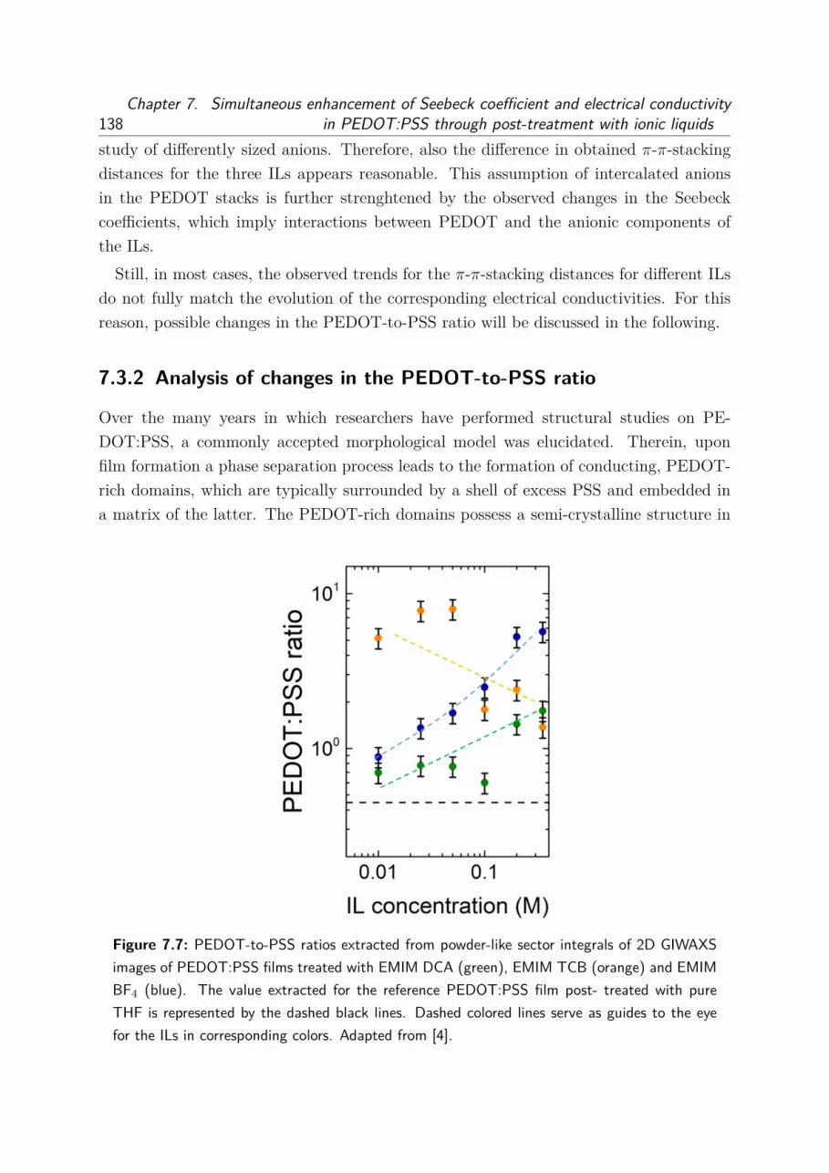
138Chapter 7. Simultaneous enhancement of Seebeck coefficient and electrical conductivity
in PEDOT:PSS through post-treatment with ionic liquidsstudy of differently sized anions. Therefore, also the difference in obtained π-π-stackingdistances for the three ILs appears reasonable. This assumption of intercalated anionsin the PEDOT stacks is further strenghtened by the observed changes in the Seebeckcoefficients, which imply interactions between PEDOT and the anionic components ofthe ILs.
Still, in most cases, the observed trends for the π-π-stacking distances for different ILsdo not fully match the evolution of the corresponding electrical conductivities. For thisreason, possible changes in the PEDOT-to-PSS ratio will be discussed in the following.
7.3.2 Analysis of changes in the PEDOT-to-PSS ratio
Over the many years in which researchers have performed structural studies on PE-DOT:PSS, a commonly accepted morphological model was elucidated. Therein, uponfilm formation a phase separation process leads to the formation of conducting, PEDOT-rich domains, which are typically surrounded by a shell of excess PSS and embedded ina matrix of the latter. The PEDOT-rich domains possess a semi-crystalline structure in
Figure 7.7: PEDOT-to-PSS ratios extracted from powder-like sector integrals of 2D GIWAXSimages of PEDOT:PSS films treated with EMIM DCA (green), EMIM TCB (orange) and EMIMBF4 (blue). The value extracted for the reference PEDOT:PSS film post- treated with pureTHF is represented by the dashed black lines. Dashed colored lines serve as guides to the eyefor the ILs in corresponding colors. Adapted from [4].

7.3. Structural characterization 139
which the π-π-stacking of PEDOT chains is prevalent, and thus allow for charge-transportwithin the domains. Barriers for the transport of charge carriers arise at the interfacesbetween the conducting, PEDOT-rich domains and the PSS matrix, since PSS itself iselectrically insulating. Therefore, it is generally believed that, while PSS aids in thedispersion of PEDOT in aqueous solution, it is detrimental to the macroscopically mea-surable electrical conductivity of the film. Most treatments, which have been devisedfor the improvement of electrical properties in PEDOT:PSS films, thus aim at selectiveinteractions with PSS for its removal from the film. ILs are expected to have a similareffect, in that the positively charged EMIM-cations can interact with the polyanion PSSelectrostatically, and thus aide in the removal of the latter from the films. To this end,the sector integrals shown in Figure 7.5 are analyzed regarding changes in the relativeamounts of PEDOT and PSS through analysis of the characteristic scattering signalsof both components. For our purposes a larger PEDOT-to-PSS ratio is more favorablefor charge transport, since charges can then be transported more easily between differ-ent conducting, PEDOT-rich domains and should therefore result in improved electricalconductivities.
The results of this analysis are shown in Figure 7.7. For all ILs an improvement com-pared to the reference value of 0.42 can be seen. This reference value is fairly close tothe nominal specification of the manufacturer, regarding the PEDOT-to-PSS ratio inthe PH1000 formulation. Especially in the cases of EMIM DCA and EMIM BF4 thePEDOT-to-PSS ratio increases as function of IL concentration. This implies a favorableeffect on the electrical conductivity, as PSS is usually considered detrimental to chargetransport within the polymer thin film. Notably, the achieved PEDOT-to-PSS ratio isfor the highest concentration of 0.35 M, is highest for EMIM BF4. On the other hand,EMIM TCB seems to be able to efficiently remove PSS at low concentrations. However,with increasing amount of EMIM TCB a slightly adverse effect on the PEDOT-to-PSSratio is observed.
Still, it can be concluded that the notion of selective electrostatic interactions betweenthe cations of the ILs and the polyanion PSS holds for all ILs. As a consequence, PSSis removed from the film during the spin-coating process and leads to a morphologicalre-organization. The loss of insulating PSS is advantageous in terms of the electricalconductivity, as charge carriers can be transported more easily through the film. For allthree ILs the increase in the PEDOT-to-PSS ratio is deemed a contributing factor in theenhancement of the electrical conductivity.

140Chapter 7. Simultaneous enhancement of Seebeck coefficient and electrical conductivity
in PEDOT:PSS through post-treatment with ionic liquids7.3.3 Analysis of preferred orientation
Figure 7.8 shows the ratio of PEDOT crystallites oriented in edge-on to face-on direction.A higher ratio is preferable, since a larger degree of edge-on orientation also impliesimproved charge transport capabilities in in-plane direction. The ratio was calculatedfrom the division of peak areas of scattering signals which are typically assigned to π-π-stacking of PEDOT chains in both edge-on and face-on orientation.
The reference PEDOT:PSS film exhibits a ratio close to one, suggesting a balance be-tween PEDOT π-π-stacks oriented in edge-on and face-on direction. Upon post-treatmentof the PEDOT:PSS films, differences between the employed ILs can be discerned. EMIMDCA- and EMIM TCB-treated films show a very low ratio, indicating an unfavorablepredominant orientation of PEDOT stacks in face-on direction. In comparison to this,low concentrations of EMIM BF4 show much larger values for the ratio which could bean explanation for the comparatively higher electrical conductivities obtained for thesesamples. While for EMIM BF4-treated samples a maximum edge-on to face-on ratio is
Figure 7.8: Edge-on to face-on ratio extracted from the respective sector integrals of 2D GI-WAXS images of PEDOT:PSS films treated with EMIM DCA (green), EMIM TCB (orange) andEMIM BF4 (blue). The ratio extracted for the reference PEDOT:PSS film post-treated withpure THF is represented by the dashed black lines. Dashed colored lines serve as guides to theeye for the ILs in corresponding colors. Adapted from [4].

7.4. Structure-conductivity correlation 141
obtained at intermediate concentrations, this drops again to a value close to that of thereference for high concentrations. In the case of EMIM TCB and EMIM DCA a steadyincrease as function of concentration is observed. This is in line with the increasing elec-trical conductivity as function of IL concentration. It can be concluded that especially forEMIM TCB- and EMIM DCA-treated films the orientation is most favorable at high con-centrations, while in the case of EMIM BF4-treatment the fraction of edge-on orientationis sufficiently high for all concentrations.
7.4 Structure-conductivity correlation
Figure 7.9 is a visual representation of the results from the morphological characteriza-tion using GIWAXS, discussed above. It summarizes the changes in the obtained π-π-
Figure 7.9: Morphological model of PEDOT:PSS treated with pure THF as reference (top left),treated with EMIM DCA (top right), EMIM TCB (bottom left) and with EMIM BF4 (bottomright). Values for the average π-π-stacking distances in both face-on (left) and edge-on (right)are given, respectively. The schematics in the center of the figure represent differences in thethree main structural quantities discussed, with PEDOT-rich crystallites (dark blue) embedded ina PSS-rich matrix (light blue). Average π-π-stacking distances are schematically shown as blacklines inside the PEDOT-rich crystallites in different densities, depending on the magnitude of therespective π-π-stacking distances. The PEDOT-to-PSS ratio is represented by the color gradientfrom dark blue (PEDOT-rich) to light blue (PSS-rich) inside the PEDOT-rich crystallites. Thepredominant orientation of the PEDOT π-stacks is represented by the stacking direction of theblack bars inside the PEDOT crystallites. Taken from [4].

142Chapter 7. Simultaneous enhancement of Seebeck coefficient and electrical conductivity
in PEDOT:PSS through post-treatment with ionic liquidsstacking distances, PEDOT-to-PSS ratios and edge-on to face-on ratios for the referencePEDOT:PSS film, as well as for the IL-treated ones.
For pristine PEDOT:PSS, average π-π-stacking distances in face-on and edge-on direc-tion are 3.70 A and 3.65 A, respectively. The determined PEDOT-to-PSS ratio is veryclose to the nominal one provided by the manufacturer, and amounts to roughly 0.37.Regarding the orientation of PEDOT π-stacks, there is a balance between face-on andedge-on orientation as shown by the equal distribution of stacks among the PEDOT crys-tallites.
EMIM DCA-treated films show π-π-stacking distances of 3.45 A and 3.65 A in face-onand edge-on, and therefore a much denser stacking in face-on direction than the reference.While initially low, the PEDOT-to-PSS ratio strongly increases in edge-on direction asfunction of concentration. In face-on direction it appears to be concentration-independent.Treatment of PEDOT:PSS with high concentrations of EMIM DCA also favorably altersthe predominant orientation of PEDOT π-stacks towards a larger degree of edge-on ori-entation. The strong improvement in the electrical conductivity of these samples can beassigned to the combination of an improved PEDOT-to-PSS ratio and re-orientation intoan edge-on configuration.π-π-stacking distances in EMIM TCB-treated films are 3.35 A and 3.60 A in face-on
and edge-on direction, respectively. In edge-on direction this is a slight improvementcompared to the reference, as smaller π-π-stacking distances correlate with improvedinter-chain charge transport. In face-on direction the difference is much more drastic, asthe smallest distances are achieved here. For both the face-on and edge-on direction adecrease of the PEDOT-to-PSS ratio as function of concentration is observed. This is morepronounced for the face-on direction, but is in general unfavorable for inter-grain chargetransport between different PEDOT-rich domains, as more insulating PSS is present.Also for the EMIM TCB-treatment a favorable re-orientation of PEDOT π-stacks into amore predominant edge-on configuration is observed, especially for high concentrations.Both the advantageous orientation and enhanced inter-chain charge transport are in linewith the increasing electrical conductivity, while the comparatively lower PEDOT-to-PSSratios are detrimental due to impeded inter-grain charge transport.
For low concentrations, the π-π-stacking distances in EMIM BF4-treated samples aremuch larger in both face-on and edge-on direction. At high concentrations they decrease to3.70 A and 3.71 A, and are therefore close to the reference value of pristine PEDOT:PSS.The PEDOT-to-PSS ratios in both face-on and edge-on direction change favorably asfunction of concentration, while the increase in face-on direction is more pronounced thanin the edge-on case. Regarding the ratio of edge-on to face-on orientation, a maximum isseen at intermediate concentrations, with the remaining samples exhibiting values close

7.5. Summary 143
to that of the reference. Both π-π-stacking distances and edge-on to face-on ratios areclose to the values seen in the reference sample, wherefore the high PEDOT-to-PSS ratiosare suggested as main driving force behind the improvement in electrical conductivities.
In conclusion, GIWAXS allowed to determine the great impact ILs have on the structureof PEDOT:PSS. The manifold effects include changes in the π-π-stacking distances, thePEDOT-to-PSS ratio and the edge-on to face-on ratio. Different ILs influence theseproperties differently, even though the cations which chosen to be the same. As discussedabove, this might originate from changes in the intrinsic properties of the ILs due tothe charge localization on the anions. It can be expected that this changes the way inwhich the EMIM cations can interact with the negatively charged PSS. Also changes inthe π-π-stacking distances could be assigned to possible inclusion of the anions into thestructure, which would explain how they evolve differently as function of IL type.
7.5 Summary
This chapter deals with the simultaneous improvement of Seebeck coefficients and elec-trical conductivities through post-treatment of PEDOT:PSS films with ILs. The binarynature of PEDOT:PSS is complemented by the ionic nature of the ILs in that the latters’anions selectively interact with PEDOT, while the cations selectively interact with PSS.Ramifications on both the Seebeck coefficient and the electrical conductivity are expected.
In order to study changes in the electronic structure, which strongly influences theobtainable Seebeck coefficients, UV-Vis spectroscopy is performed. It reveals differentinteractions of the anions with PEDOT, which conforms to the observation of changesin the Seebeck coefficients for the three employed ILs. Treatment with EMIM DCAleads to the highest Seebeck coefficients around 40µV/K, which can be explained by theemergence of absorption features that can be assigned to both polaronic and neutral statesin PEDOT chains. EMIM BF4-treatment leads to slightly improved Seebeck coefficientsof approximately 30µV/K, and is explained by the sole emergence of polaronic bands. Alack of new absorption features for EMIM TCB-treated samples is in line with the Seebeckcoefficients being around the reference value of approximately 20 µV/K. The trends areexplained through the charge distribution on the respective anions, with the DCA-anionshowing the highest degree of charge localization due to its angulated structure. Thespherically symmetrical BF4- and TCB-anion differ in their overall size, with the latterbeing larger because of its biatomic ligands. Therefore, the higher charge density ofthe BF4-anion leads to improved interactions with PEDOT and thus to higher Seebeckcoefficients. Additionally, the hydrogen-bond basicity is identified as possible parameterwith which changes in the Seebeck coefficients can be predicted.
144Chapter 7. Simultaneous enhancement of Seebeck coefficient and electrical conductivity
in PEDOT:PSS through post-treatment with ionic liquidsGIWAXS is used to study the structure of PEDOT:PSS and potential changes upon
treatment with the different ILs. The investigation was carried out focusing on aver-age π-π-stacking distances, the PEDOT-to-PSS ratio and the edge-on to face-on ratio.Changes in the π-π-stacking distances strongly depend on the employed ILs as vastlydifferent trends and average values are found as function of both type and concentrationof IL used for post-treatment. Especially for treatment with EMIM DCA and EMIMTCB lower π-π-stacking distances are observed, which contribute to improved inter-chaincharge transport. Intercalation of anions into the PEDOT π-stacks is proposed as possiblemechanism. Also regarding the PEDOT-to-PSS, changes between the ILs are discernible.In most cases, PSS is removed from the film due to its electrostatic interactions withthe EMIM cations, leading to larger PEDOT-to-PSS ratios. EMIM TCB shows adversetrends for both the face-on and edge-on orientation, while still being improved comparedto the reference value. Thus, especially for treatment with EMIM DCA and EMIM BF4
the inter-grain charge transport is improved. The edge-on to face-on ratio gives insightinto preferred directions of charge transport, with a higher fraction of PEDOT π-π-stacksoriented edge-on being favorable for high electrical conductivities. Treatment with EMIMBF4 leads to a maximum at intermediate concentrations, while EMIM DCA- and EMIMTCB-treatments lead to greatly increased ratios especially at high concentrations. Allfindings are compiled in the morphological model shown in Figure 7.9.
In summary, post-treatment of PEDOT:PSS with IL is a promising approach at im-proving the thermoelectric properties of thin films of the former. This is achieved bythe simultaneous enhancement of the Seebeck coefficient and the electrical conductivity.Through the rational choice of ILs used in this study, in which the cations are the sameand only the anions differ, many interesting features of the treatment are found. Firstly,the structure of the anion has serious ramifications on the resulting Seebeck coefficients,as the former are expected to primarily interact with the conjugated PEDOT. Therein,a stronger localization of the negative charge on the anion appears to be more favorablefor the achievement of high Seebeck coefficients. The notion of the variation of the anionnot influencing the electrical conductivity is proven to be incorrect. The properties of theanion greatly influence the intrinsic properties of the ILs, and therefore affect the inter-action with PSS. This is seen in the differing dependencies of the investigated structuralparameters on the type of IL. This study provides a starting point for further investiga-tions in which the impact of other anions with different structural motives can be studied.The vast catalogue of possible combinations of cations and anions in ILs opens a largewindow of tunability of thermoelectric properties in PEDOT:PSS.

8 P(NDI2OD-T2) as n-type polymerfor thermoelectric applications
This chapter is largely based on the results obtained with Regina Kluge in the frameworkof her master’s thesis. [25]
Since their inception, conducting polymers have experienced a growth in popularityamongst researchers. This led to a strong emphasis on the synthesis of new materials,which were expected to possess interesting properties especially for application in opto-electronics, e.g. in transistors, organic solar cells, etc. As a result, a plethora of differentpolymers were fabricated with a large window of tunability regarding energy levels of theHOMO and LUMO of those materials.
While polymers with the ability to transport positive charges are comparatively easyto synthesize, due to their structural simplicity, the opposite is the case for polymers withthe ability to transport negative charge carriers. Restrictions regarding the inclusion ofgroups with the ability to transport negative charges and stability, among others, makethese polymers usually very complex on atomic scales. This caused a certain neglectionof these polymers, regarding both, their basic characterization and potential applicationin organic electronics. This work attempts to understand the mechanisms determiningthe properties of n-type polymers by studying a commonly used representative, namelyP(NDI2OD-T2).
In this study, the well-known alternating copolymer P(NDI2OD-T2) is studied regard-ing the influence of doping with a benzimidazoline derivative on optical, morphological andthermoelectric properties. For this purpose, UV-Vis spectroscopy is performed on dopedfilms in order to investigate changes in the electronic structure, and link those to thermo-electric measurements of the doped films. GIWAXS is used to study the structure of thepristine polymer thin film and changes thereof upon doping. Regarding the thermoelec-tric characterization, different sample geometries are employed, and examined regardingthe feasibility of their usage in thermoelectric generators. Thermoelectric quantities aremeasured along and perpendicular to the sample-substrate interface in these differentgeometries. Based on these results, a comprehensive model is given which sums up the
145

146 Chapter 8. P(NDI2OD-T2) as n-type polymer for thermoelectric applications
findings of the spectroscopic and morphological analysis and links those to the observedthermoelectric properties.
P(NDI2OD-T2) is combined with PEDOT:PSS in order to fabricate a thermoelectricgenerator based on polymers as active materials.
8.1 Spectroscopic characterization using UV-Visspectroscopy
Intrinsically, P(NDI2OD-T2) is an electrical insulator. Therefore, doping of the conduct-ing polymer is required in order to introduce charge carriers and thereby enable chargetransport. In this case, P(NDI2OD-T2) is doped with a benzimidazoline derivative calledN-DPBI in different concentrations. The effect of doping is studied using UV-Vis spec-troscopy, similarly to how it was used on PEDOT:PSS films in order to investigate changesin the charge carrier concentration. More specifically, UV-Vis spectra are analyzed re-garding the appearance and disappearance of features as function of dopant concentration,but also as function of temperature in order to understand the stability of doped films.
8.1.1 Influence of dopant concentration
The employed dopant N-DPBI is expected to transfer negative charges in form of electronsor hydride ions onto the polymer P(NDI2OD-T2) in order to increase the charge carrierdensity. To find out how this reaction proceeds, solutions of the dopant in dichlorobenzene
Figure 8.1: Photographic comparison of N-DPBI solutions in chlorobenzene stored either inambient atmosphere (top row) or a nitrogen-filled glovebox (bottom row, indicated by the dashedboxes) when subjected to different temperatures. Temperatures are increasing from left to right,as indicated by the arrow. For the final photo on the right, both solutions were transferred intothe glovebox.

8.1. Spectroscopic characterization using UV-Vis spectroscopy 147
Figure 8.2: Presumed redox reaction of dopant N-DPBI in solution, under hydrogen transferfollowing Wei et al. [77]
are subjected to different temperatures, with one vial being stored in a nitrogen-filledglovebox, and the other one being stored in ambient atmosphere. Figure 8.1 shows theresults for both solutions. Notably, there is a distinct difference in color between the twosolutions, as the one stored in air exhibits a yellow color for temperatures exceeding 60 C,while the solution stored in nitrogen atmosphere remains colorless. There are two thingsthat can be learned from this experiment. Firstly, a reaction of the dopant only takesplace with an appropriate reaction partner, which in this case was most likely oxygenfrom the atmosphere. Secondly, a certain temperature has to be exceeded for the dopantto react.
The presumed reaction is shown in Figure 8.2, as proposed by Wei et al. [77] Thesplitting off of a hydrogen atom, which must be activated by an energy transfer to thedopant, e.g. by increasing temperature, is followed by the loss of an electron, leaving theoxidized form of the dopant. Under re-organization of bonds, an extended conjugated π-system is formed, which could be a viable explanation for the occurrence of a yellow color.Thus, it is concluded that in order for the reduction reaction to occur, P(NDI2OD-T2)and N-DPBI have to be combined at elevated temperature in nitrogen atmosphere toensure successful transfer of the negative charge to the polymer.
Doped thin films of P(NDI2OD-T2) are prepared as outlined in Section 4.2.4, makinguse of the findings of the preliminary experiment discussed above. UV-Vis spectroscopy,as seen in previous chapters, can be used to deduce the electronic structure of a conductingpolymer, as charge carriers can be typically excited electronically using light and thereforeyield characteristic features in the spectra. The UV-Vis spectra for films doped withup to 40 wt% N-DPBI are shown in Figure 8.3. In the pristine state, P(NDI2OD-T2)already shows two interesting features, one at lower and one at higher wavelengths, whichoriginates from its donor-acceptor copolymer structure. As discussed by Steyrleuthner etal., the former peak can be associated to the presence of π-π-stacks of P(NDI2OD-T2)chains in solution, which can be also found after deposition on a substrate. [78] Through

148 Chapter 8. P(NDI2OD-T2) as n-type polymer for thermoelectric applications
stacking, an extended π-system is formed, which can be excited electronically by UV-light. The second feature originates from the donor-acceptor nature of the polymer.While the naphthalene-diimide possesses electron-accepting properties, the bithiophene-unit shows electron-donating properties. The redistribution of electrons from the donorto the acceptor moiety can be stimulated with visible light, which is also why reason thatthe pristine film shows a vibrant turquoise color, as seen in Figure 8.3. Changes in theseintrinsically occurring features not only give information on the electronic structure, butalso on changes in the morphology due to interaction with the dopant molecules. Upondoping with N-DPBI, a general decrease of intensity of the aforementioned features isobserved in addition to a blue-shift of the low-wavelength peak. In the case of the low-wavelength band, the blue-shift is an indication of less efficient π-π-stacking, possibly dueto incorporation of the dopant molecules within the intrinsically present π-π-stacks, whichwill be discussed in greater detail in the morphological analysis below. The decrease of thecharge-transfer band at high wavelengths may be indicative of changes in the conformationof the chains, respectively the orbital overlap between the donor- and acceptor-moietieswithin the chains. Nevertheless, additional absorption features appear at around 500 nmand 800 nm, which are indicators for the presence of negative polaronic species, as foundby Caironi and co-workers. [79] All these findings support the notion of charge transferfrom the dopant N-DPBI to P(NDI2OD-T2), with an indication of incorporation of thedopant into the π-π-stacks of the polymer, which will be discussed in more detail below.
8.1.2 Influence of temperature
A general problem one encounters with n-type conducting polymers is their instability to-wards oxidation in an ambient atmosphere. The reaction with oxygen in general createsadditional states which trap negative charge carriers, and thereby inhibit their trans-port. It can be expected that this process is facilitated and accelerated by increasing thetemperature of the films. Therefore, temperature-dependent UV-Vis measurements areperformed for films doped with different concentrations of N-DPBI, which are compiledin Figure 8.4.
While temperature-dependent UV-Vis measurements are performed, reference measure-ments at room temperature are carried out at the same time with films of the same dopantconcentration. Since the oxidation and therefore degradation of the films is also expectedto happen in ambient conditions, these measurements are performed while the samplesat room temperature in order to pinpoint the influence of temperature on the appearanceor disappearance of certain features. Similarly to Figure 8.3, doped P(NDI2OD-T2) filmsshow gradual decrease in the π-π-stacking and charge-transfer contribution to the spectra

8.1. Spectroscopic characterization using UV-Vis spectroscopy 149
Figure 8.3: a) UV-Vis spectra of P(NDI2OD-T2) thin films on glass doped with differentconcentrations of N-DPBI, as indicated in the legend. b) Photographs of P(NDI2OD-T2) thinfilms doped with the corresponding concentrations of N-DPBI.
found close to 370 nm and 700 nm. In addition, bands assigned to the presence of neg-ative polarons appear at 500 nm and 800 nm, indicating successful doping. The changesin the reference spectra hint at re-oxidation of the doped polymer films. Interestingly,also for the pristine film in Figure 8.4 minute changes are detected, since the absorbanceof both the π-π-stacking and charge-transfer peaks increases slightly over time. In thecase of doping in concentrations of 40 wt%, significant changes in the spectra are mostapparent after approximately 50 min, since the absorbance of the polaron peaks foundat 500 nm and 800 nm decrease, and the charge-transfer peak slightly increases again.Regarding the influence of temperature, similar trends are found, although to a largerextent. As discussed before, oxidation of the doped polymer leads to the formation oftrap states which manifest themselves as decrease of the polaronic contributions to thespectra. Temperatures above 70 C seem to vastly accelerate the oxidation process, whichcan be most clearly seen from the sample with the highest concentration of N-DPBI inthe bottom right corner of Figure 8.4, but is expected to be similar for the other investi-gated concentrations. There is a steep decrease in the absorbance of the high-wavelengthpolaronic band for temperatures of 80 C and higher, which coincides with the simulta-neous drastic increase in absorbance of the charge-transfer peak. For all investigations

150 Chapter 8. P(NDI2OD-T2) as n-type polymer for thermoelectric applications
Figure 8.4: Temperature-dependent UV-Vis measurements of doped P(NDI2OD-T2) films inconcentrations of a) 0 wt%, b) 5 wt%, c) 10 wt%, d) 20 wt% and e) 40 wt%. In addition, azoom-in of the 40 wt% sample spectrum in the high wavelength region is shown in the bottomright of the figure, in order to highlight the effect of degradation due to temperature. Sincethe measurements were carried out in ambient atmosphere, reference measurements at roomtemperature were carried out simultaneously to the temperature-dependent ones and are shownas the top graph for each dopant concentration. Both measurements were carried out simultane-ously in intervals of 10 min. In the temperature dependent measurement, the temperature wasramped from room temperature to 100 C in steps of 10 C while the reference measurementwas conducted at room temperature.

8.2. Structure characterization using grazing-incidence wide-angle x-ray scattering 151
of the thermoelectric properties, this critical temperature of 80 C will be taken avoidedwhen performing the measurement of the Seebeck coefficient and temperature-dependentresistances of the doped P(NDI2OD-T2) films.
In summary, UV-Vis spectroscopy represents a facile and non-destructive method ofconfirming successful doping of P(NDI2OD-T2) thin films with different concentrations ofN-DPBI. Additionally, performing temperature-dependent UV-Vis measurements allowsfor understanding the role of oxygen and elevated temperatures on the degradation processof the doped polymer films. It becomes thus possible to take degradation of the filmsduring characterization into account and to adjust the measurement protocol accordingly,as will be discussed further on.
8.2 Structure characterization using grazing-incidencewide-angle x-ray scattering
As previously discussed, doping of P(NDI2OD-T2) films with N-DPBI as small moleculardopant has implications on the electronic structure of the conducting polymer. However,since as opposed to inorganic semiconductors the concentrations are not in the parts permillion (ppm) or parts per billion range, but instead amount to a significant fraction ofmaterial in solution, ramifications on the final structure in the thin film are expected.Therefore, after a short literature review of previous studies on the structure, GIWAXSwill be performed on P(NDI2OD-T2) films fabricated on glass and FTO substrates. Aswill be seen in Section 8.3, different substrates are used for the different measurementgeometries for the thermoelectric characterization of the films. This study will thus helpin understanding potential differences and if the final film structure is influenced by thesubstrate or not.
Due to P(NDI2OD-T2) being an alternating copolymer, it shows several interestingstructural features, which will be discussed in the following. [80–87] On a molecular level,each monomer unit can be divided into the napthalene-diimide acceptor-subunit and thebithiophene donor-subunit. As per several studies, these subunits are believed to betilted against each other, which can be seen in more detail in Figure 8.5a. Going tosupermolecular lengthscales, the polymer chains are expected to form aggregates due toπ-π-stacking. In the specific case of P(NDI2OD-T2) this can potentially happen in twoways: either by segregated stacking (e.g. donor-donor and acceptor-acceptor stacking)or by a mixed stacking. Both versions are depicted in 8.5b. Due to the separationof the naphtalene-diimide subunits by thiophene units, whereas the latter ones do notcontribute to negative charge transport, a segregated π-π-stacking would be preferred,

152 Chapter 8. P(NDI2OD-T2) as n-type polymer for thermoelectric applications
Figure 8.5: Proposed morphological model for P(NDI2OD-T2), combining different findingsfrom literature. [89] a) Structure of a single P(NDI2OD-T2) monomer, highlighting the tiltbetween the acceptor- (red) and donor-subunit (green). b) Polymer chains interact with eachother via segregated or mixed π-stacking and thereby build up lamellae, as indicated by theturquoise boxes. c) Crystallites consisting of lamellar stacks of P(NDI2OD-T2), with the formerarranging in a face-on manner with respect to a substrate when fabricated as thin film. Smalldegrees of tilt represent deviations from a perfect horizontal alignment of the crystallites on thesubstrate.
since this would allow charge transport between different chains. [88] The π-stacks areconnected through the bithiophene units along the direction of the polymer chains andarrange on another length scale in a lamellar fashion. The lamellae formed by the extendedpolymer chains are highlighted by the turquoise boxes containing the π- stacks in Figure8.5b. Steyrleuthner et al. measured the vertical electron mobility in unipolar diodes.They revealed that crystallinity along the π-π-stacking direction is highly important forachieving high charge carrier mobilities. However, the alkyl side chains create barriers forcharge carrier transfer in lamellae, whose ordering plays little role in charge transport. [87]Still, the lamellar stacking in horizontal direction leads to the formation of flat crystallites,which are depicted in Figure 8.5c. In a thin film these crystallites are arranged in a face-on manner, and stack upon each other, with slight deviations to a perfect horizontalalignment thereof.
In summary, a preferential orientation of the π-stacks perpendicular to the plane of thecrystallites is found, while inside the crystallites themselves are built-up by in-plane in-teraction of regions where polymer chains are regularly ordered via π-stacking, also calledlamellae. The crystallites preferably rest on top of the substrate being aligned, i.e. in aface-on manner. Since charge transport is assumed to take place along the π-stacks, [87]it can be concluded that for the pristine P(NDI2OD-T2) film charge transport is assumed
8.2. Structure characterization using grazing-incidence wide-angle x-ray scattering 153
to be most efficient perpendicular to the substrate. The question that then arises is, ifdoping of the polymer with N-DPBI in different concentrations influences the structure ofthe polymer. This question will be discussed in terms of ordering perpendicular and alongthe substrate, and in the preferential orientation which is adopted by the π-stacks, whichin turn will influence the orientation of the crystallites. For the investigated in-plane andcross-plane measurement geometries discussed below in Section 8.3, P(NDI2OD-T2) filmswere prepared on glass substrates. This way, in in-plane measurements, charge transportis probed parallel to the substrate. FTO-coated glass substrates are used for cross-planeand pseudo-in-plane measurements, with the charge transport having being primarilyprobed in the respective directions. Therefore, GIWAXS measurements are carried outwith samples in the corresponding sample geometries.
8.2.1 P(NDI2OD-T2) films on glass substrates for in-planemeasurements
Firstly, doped P(NDI2OD-T2) films are prepared on insulating glass substrates. Glass is awell-suited substrate material for the measurement of thermoelectric properties along thesubstrate, since it itself is insulating and therefore does not influence the measurements.Dopant concentrations are chosen in conformity with the spectroscopic characterizationdiscussed above, in order to link electronic and morphological properties of the dopedP(NDI2OD-T2) films in order to find a link.
Figure 8.6 shows the 2D GIWAXS patterns as function of N-DPBI concentration. Sev-eral distinct scattering features are present for the pristine P(NDI2OD-T2) film, which arehighlighted by the white circles in Figure 8.6a. In qz-direction, the signal at large q-valuesis typically assigned to the segregated π-π-stacking discussed above. The fact that thesignal is oriented in the z-direction also indicates the predominant direction of the stackingin the same direction. As discussed above, the lamellar stacking in the pristine polymerfilm is in in-plane direction. Therefore, the corresponding peaks in the 2D GIWAXS pat-tern can be found in qxy-direction. The first order of the lamellar stacking peak is locatedat around 0.25 A−1. With increasing dopant concentration a corresponding peak emergesat the same value but in qz-direction. It is represented by the first-order scattering peakin qz-direction found at values of approximately 0.25 A−1. These findings are consistentwith the morphological picture previously drawn by other researchers. Upon doping, thescattering patterns change, as indicated by loss of signals and rearrangement of scatteringpeaks.
Sector integration within 2D GIWAXS patterns allows analysis of the crystallinity in thepolymer film perpendicular to the plane of the substrate. Figure 8.7a shows the evolution

154 Chapter 8. P(NDI2OD-T2) as n-type polymer for thermoelectric applications
Figure 8.6: 2D GIWAXS data of P(NDI2OD-T2) films on glass substrates doped with a) 0 wt%,b) 5 wt%, c) 10 wt%, d) 20 wt% and e) 40 wt% N-DPBI. For the 0 wt% sample, the π-π-stacking peak is denoted with (010), while the signals ascribed to in-plane (ip) lamellar stackingare denoted with (100)ip and (200)ip. Due to re-orientation upon dedoping, lamellar stacking isfound in out-of-plane (op) direction, with the corresponding signals being denoted by (100)op,(200)op and (300)op.

8.2. Structure characterization using grazing-incidence wide-angle x-ray scattering 155
of vertical sector integrals as function of doping concentration. With increasing valuesof q, the above-mentioned structural features in the following order: first-order lamellarstacking, second-order crystallite stacking, third-order lamellar stacking and finally π-π-stacking. While the former two appear to shift towards larger q-values, and even athird-order peak arises at q-values of around 0.8 A−1, which can also be seen in Figure8.7b, the intensity of the π-π-stacking peak at q-values of approximately 1.6 A−1 seemsto decrease as function of dopant concentration. While the latter is indicative of loss inorder on very small length-scales in vertical direction, the combination of peak shifts, newpeaks arising and the practically unchanged peak widths will be discussed below, afterthe discussion of the horizontal sector integrals.
Figure 8.7: a) Vertical sector integrals obtained from 2D GIWAXS data of P(NDI2OD-T2)films prepared on glass with varying doping concentrations: 0 wt% (yellow), 5 wt% (magenta),10 wt% (green), 20 wt% (brown) and 40 wt% (black). Inset: exemplary 2D GIWAXS pattern,with the integrated area marked by dashed gray lines. b) q-positions of peaks, c) peak widthsand d) peak amplitudes as function of doping concentration.

156 Chapter 8. P(NDI2OD-T2) as n-type polymer for thermoelectric applications
Sector integration in horizontal direction reveals crystalline structures parallel to thesubstrates, and therefore are of great importance for change transport in in-plane di-rection, which is measured for the P(NDI2OD-T2) films prepared on glass. Figure 8.8ashows the horizontal sector integrals as function of dopant concentration. Two promi-nent scattering features can be discerned which are assigned to the first and second orderof lamellar stacking of P(NDI2OD-T2) chains, with increasing q-values. For low con-centrations up to 10 wt% also a third order peak is visible. As explained above, theπ-π-stacks of P(NDI2OD-T2) chains extend perpendicular to the polymer backbone. Asexplained above, extended polymer chains of P(NDI2OD-T2) interact with each other viaπ-π-stacking and thereby build up sheet-like regions of regular chain arrangement which
Figure 8.8: a) Horizontal sector integrals obtained from 2D GIWAXS patterns of P(NDI2OD-T2)films prepared on glass with varying doping concentrations: 0 wt% (yellow), 5 wt% (magenta),10 wt% (green), 20 wt% (brown) and 40 wt% (black). Inset: exemplary 2D GIWAXS pattern,with the integrated area marked by dashed gray lines. b) q-positions of peaks, c) peak widthsand d) peak amplitudes as function of doping concentration.

8.2. Structure characterization using grazing-incidence wide-angle x-ray scattering 157
are called lamellae. These lamellae in turn stack with each other and thereby createflat plate-like crystallites. In the pristine polymer, this lamellar stacking is believed totake place in in-plane direction, which can be confirmed in the GIWAXS measurementspresented here, since the corresponding peaks appear in qxy-direction. With increasingconcentration of N-DPBI, a shift of the first order towards higher q-values is observed,which indicates denser lamellar stacking, as seen in Figure 8.8b. Meanwhile, the secondorder peak position is almost constant, whereas the third order peak also moves towardslarger q-values. Figure 8.8c shows that the peak widths of the first and second orderstay mostly constant, while their respective intensities decrease as function of dopantconcentration. The second order is no longer detectable for a dopant concentration of40 wt%, which hints at a loss of order in lamellar stacking as compared to the pristineP(NDI2OD-T2) film.
GIWAXS also allows for the analysis of predominant orientation of crystallites (whichcan only be measured indirectly through the orientation of the lamellar stacking) and/orstackings. In this case, the orientation of both the first lamellar stacking and the π-π-stacking is analyzed by performing azimuthal integration of intensities for q-values be-tween 0.2 A−1 and 0.3 A−1. The corresponding results are shown in Figure 8.9 as functionof concentration. The azimuthal integrals for the first lamellar stacking peak are shownin Figure 8.9a as function of N-DPBI concentration. This peak increases and shows themaximum intensity at χ-values close to 0 for a concentration of 20 wt%, only to decreaseagain for higher dopant amounts. In addition, at large χ-values of approximately 80 , adecrease in intensity is observed for increasing dopant concentration. While large intensi-ties at χ-values close to 0 indicate predominant stacking perpendicular to the substrate,the opposite is true for large intensities at high χ-values close to 80 , being indicative oflamellar stacking parallel to the substrate. In Figure 8.9b the face-on-to-edge-on ratio isshown for the differently doped P(NDI2OD-T2) films, which is obtained through simpledivision of the respective peak amplitudes. The ratio decreases with increasing concentra-tion of N-DPBI, which can be interpreted as transition from predominant face-on stackingtowards edge-on stacking of lamellae. Since the lamellar stacking leads to the build-up ofcrystallites (see Figure 8.5), a change in stacking direction directly influences the orienta-tion of the latter. In this case, a change of lamellar stacking from in- to out-of-plane leadsto a re-orientation of the crystallites from face- to edge-on as is schematically shown inthe inset of Figure 8.9a. as schematically shown in Figure 8.9a.
The results of the analysis of ordering, which is performed by azimuthal integration forq-values from 1.58 A−1 to 1.61 A−1 for the π- π-stacking peak can be seen in Figure 8.9c.The peak, which shows a high amplitude for the pristine film, steadily loses intensity withincreasing dopant concentration and ultimately vanishes, which is also reflected in the
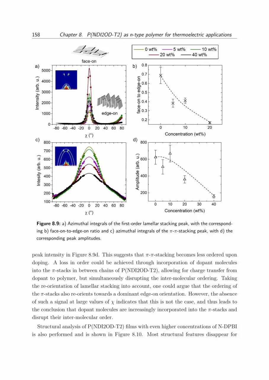
158 Chapter 8. P(NDI2OD-T2) as n-type polymer for thermoelectric applications
Figure 8.9: a) Azimuthal integrals of the first-order lamellar stacking peak, with the correspond-ing b) face-on-to-edge-on ratio and c) azimuthal integrals of the π-π-stacking peak, with d) thecorresponding peak amplitudes.
peak intensity in Figure 8.9d. This suggests that π-π-stacking becomes less ordered upondoping. A loss in order could be achieved through incorporation of dopant moleculesinto the π-stacks in between chains of P(NDI2OD-T2), allowing for charge transfer fromdopant to polymer, but simultaneously disrupting the inter-molecular ordering. Takingthe re-orientation of lamellar stacking into account, one could argue that the ordering ofthe π-stacks also re-orients towards a dominant edge-on orientation. However, the absenceof such a signal at large values of χ indicates that this is not the case, and thus leads tothe conclusion that dopant molecules are increasingly incorporated into the π-stacks anddisrupt their inter-molecular order.
Structural analysis of P(NDI2OD-T2) films with even higher concentrations of N-DPBIis also performed and is shown in Figure 8.10. Most structural features disappear for

8.2. Structure characterization using grazing-incidence wide-angle x-ray scattering 159
concentrations above 60 wt%, which suggests a complete loss of order. This strengthensthe above-mentioned theory that dopant molecules are increasingly incorporated withinthe supermolecular structure of P(NDI2OD-T2) films. Thus, concentrations of 60 wt%and 80 wt% will not be considered further.
8.2.2 P(NDI2OD-T2) films on FTO substrates for cross- andpseudo-in-plane measurements
This section discusses the evolution of the P(NDI2OD-T2) thin film structure upon dop-ing. As opposed to the previous section, here the films are prepared on FTO substratesfor measurement of thermoelectric properties in a cross-plane and pseudo-in-plane ge-ometry. Charge transport is examined perpendicular to the substrate, which requires abottom electrode realized by using FTO-coated glass substrates. GIWAXS measurementswere performed at the beamline P03 of the DESY in Hamburg, Germany. As previouslydiscussed in Section 8.1, doped P(NDI2OD-T2) are subject to degradation in an oxida-tive environment, i.e. the effect of doping diminishes when storing doped samples in air.Thusly, there is an urgent need for elucidating a proper way of transporting the dopedsamples to the measurement site.
Figure 8.11 shows exemplary UV-Vis spectra of P(NDI2OD-T2) doped with 40 wt%N-DPBI stored in two different ways. One sample was stored in a sealed aluminum-foil-composite bag, while the other one was stored in a sealed Duran-glass bottle. Spectra ofthe initial state and after five hours are shown and reveal drastic differences. While bothsamples show similar features in the initial state, namely the strongly reduced charge-transfer band around 700 nm and the increased polaron band around 500 nm, the samplesstored in the aluminum bag show signs of degradation. As opposed to the sample stored inthe Duran bottle, here the polaron band strongly reduces in intensity, while the absorbanceof the charge-transfer band again increases. This suggests lower doping levels, which inthis case can be attributed to the reaction of the doped P(NDI2OD-T2) films with oxygen.Whether this comes from a leakage in the bag, or residual oxygen trapped inside the bag(although very unlikely, since the samples were packaged inside a nitrogen-filled glovebox), remains elusive. Still, storing in a sealed Duran glass bottle appears to be a viablechoice for transportation of the samples to the measurement site at DESY. Indeed, whenthe doped samples were mounted at the instrument, they still exhibited a different colorcompared to the pristine film (see Figure 8.3b for comparison).
Successful transport of the samples allowed for GIWAXS measurements of the dopedP(NDI2OD-T2) films prepared on FTO substrates, the 2D patterns for which can be seenin Figure 8.12. FTO is typically made by a vapor deposition process on top of glass

160 Chapter 8. P(NDI2OD-T2) as n-type polymer for thermoelectric applications
Figure 8.10: 2D GIWAXS data of P(NDI2OD-T2) films doped with increasing concentration ofN-DPBI, ranging from 5 wt% to 80 wt%.
substrates. In order to avoid confusion and allow for correct assignment of scatteringfeatures to the components, exemplary 2D GIWAXS data of pristine FTO is shown asreference, along with those of the doped P(NDI2OD-T2) films. The pristine P(NDI2OD-
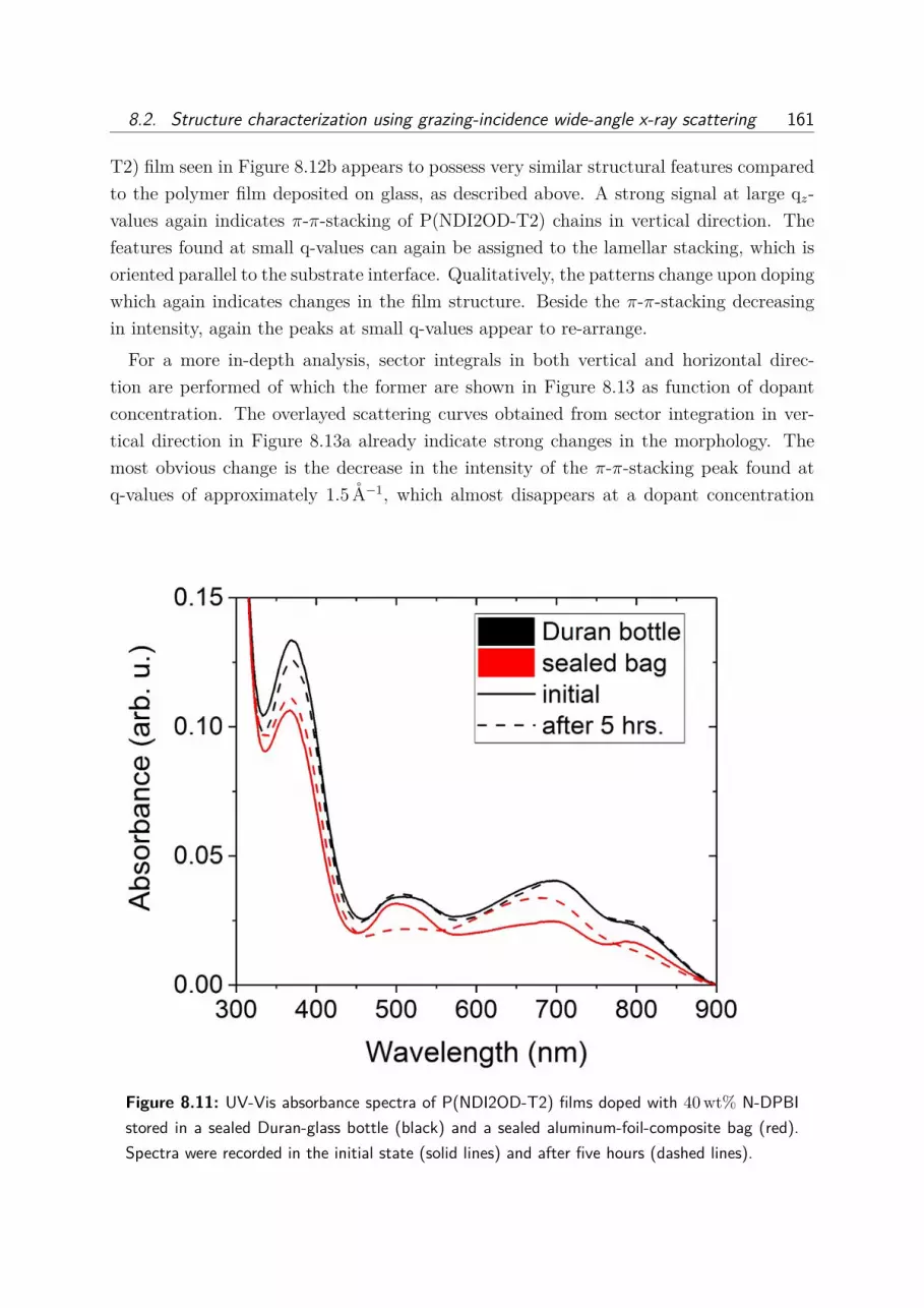
8.2. Structure characterization using grazing-incidence wide-angle x-ray scattering 161
T2) film seen in Figure 8.12b appears to possess very similar structural features comparedto the polymer film deposited on glass, as described above. A strong signal at large qz-values again indicates π-π-stacking of P(NDI2OD-T2) chains in vertical direction. Thefeatures found at small q-values can again be assigned to the lamellar stacking, which isoriented parallel to the substrate interface. Qualitatively, the patterns change upon dopingwhich again indicates changes in the film structure. Beside the π-π-stacking decreasingin intensity, again the peaks at small q-values appear to re-arrange.
For a more in-depth analysis, sector integrals in both vertical and horizontal direc-tion are performed of which the former are shown in Figure 8.13 as function of dopantconcentration. The overlayed scattering curves obtained from sector integration in ver-tical direction in Figure 8.13a already indicate strong changes in the morphology. Themost obvious change is the decrease in the intensity of the π-π-stacking peak found atq-values of approximately 1.5 A−1, which almost disappears at a dopant concentration
Figure 8.11: UV-Vis absorbance spectra of P(NDI2OD-T2) films doped with 40 wt% N-DPBIstored in a sealed Duran-glass bottle (black) and a sealed aluminum-foil-composite bag (red).Spectra were recorded in the initial state (solid lines) and after five hours (dashed lines).
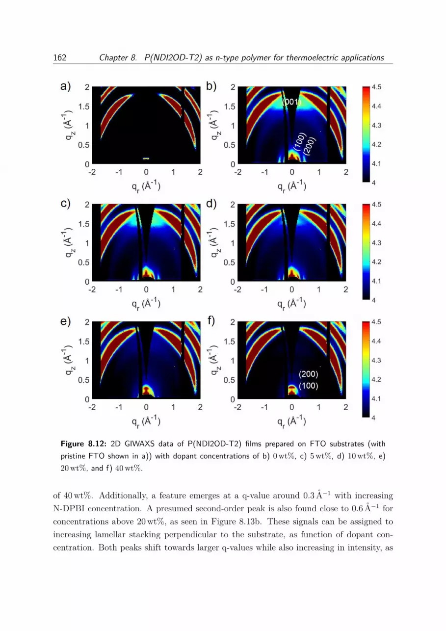
162 Chapter 8. P(NDI2OD-T2) as n-type polymer for thermoelectric applications
Figure 8.12: 2D GIWAXS data of P(NDI2OD-T2) films prepared on FTO substrates (withpristine FTO shown in a)) with dopant concentrations of b) 0 wt%, c) 5 wt%, d) 10 wt%, e)20 wt%, and f) 40 wt%.
of 40 wt%. Additionally, a feature emerges at a q-value around 0.3 A−1 with increasingN-DPBI concentration. A presumed second-order peak is also found close to 0.6 A−1 forconcentrations above 20 wt%, as seen in Figure 8.13b. These signals can be assigned toincreasing lamellar stacking perpendicular to the substrate, as function of dopant con-centration. Both peaks shift towards larger q-values while also increasing in intensity, as

8.2. Structure characterization using grazing-incidence wide-angle x-ray scattering 163
is shown in Figure 8.13d. The ramification of the peak shifts will be discussed after theanalysis of the horizontal sector integrals.
The horizontal sector integrals are shown in Figure 8.14. In the corresponding scatter-ing curves in Figure 8.14a, two distinct features can be discerned. As it was the case forP(NDI2OD-T2) films on glass, these features can again be assigned to the lamellar stack-ing of P(NDI2OD-T2) parallel to the interface of the substrate. Again, a first-order andsecond-order peak can be discerned, which shift in opposite directions upon doping withN-DPBI. Their contribution to the scattering signal diminishes with increasing dopantconcentration, which indicates loss of structural order at least in in-plane direction.
Together with the information obtained from azimuthal integration, which is shown inFigure 8.15, it becomes possible to fully elucidate the changes in the film structure upon
Figure 8.13: a) Vertical sector integrals from 2D GIWAXS data of P(NDI2OD-T2) films dopedwith 0 wt% (yellow), 5 wt% (magenta), 10 wt% (green), 20 wt% (brown) and 40 wt% (black).b) Peak positions, c) peak widths and d) peak amplitudes of the (100) (black) and (200) (blue)peak.

164 Chapter 8. P(NDI2OD-T2) as n-type polymer for thermoelectric applications
doping of P(NDI2OD-T2) with N-DPBI. Figure 8.15a shows the azimuthal line cuts asfunction of concentration for the first-order peak assigned to the lamellar stacking, per-formed for q-values between 0.2 A−1 and 0.3 A−1. While for the pristine film, intensitiesboth at χ-values around 0 and 70 are similar, the ratio changes strongly upon dop-ing. The scattering contribution at large χ-values is strongly decreased for concentrationsof 40 wt%, while the intensity around 0 remains constant. This indicates a change instacking direction, which can be analyzed in more detail, by calculating the ratio of therespective amplitudes, as is shown in Figure 8.15b. The face-on-to-edge-on ratio is gradu-ally decreasing with increasing amount of dopant, which indicates a re-orientation of thelamellar stacking from being favored parallel to the substrate in the pristine film, to beingfavored perpendicular to the substrate for high concentration. This finding qualitatively
Figure 8.14: a) Horizontal sector integrals from 2D GIWAXS data of P(NDI2OD-T2) filmsdoped with 0 wt% (yellow), 5 wt% (magenta), 10 wt% (green), 20 wt% (brown) and 40 wt%(black). b) Peak positions, c) peak widths and d) peak amplitudes of the (100) (black) and(200) (blue) peak.

8.2. Structure characterization using grazing-incidence wide-angle x-ray scattering 165
Figure 8.15: a) Azimuthal integrals of the first-order lamellar stacking peak, with the corre-sponding b) face-on-to-edge-on ratio and c) azimuthal integrals of the π-π-stacking peak, withd) the corresponding peak amplitudes.
resembles that for doped P(NDI2OD-T2) films prepared on glass substrates discussedabove. Azimuthal integration of the π-π-stacking peak (between q-values of 1.58 A−1 and1.61 A−1), again reveals the decreasing order of the π-π-stacking with increasing degreeof doping, as seen from the azimuthal line cuts in Figure 8.15c and the respective peakamplitudes in Figure 8.15d. As discussed before, this can most likely be assigned toincorporation of dopant molecules into the π-stacks, allowing for charge transfer fromthe dopant molecules to the polymer, while simultaneously destroying the order of theπ-stacks, especially at high dopant concentrations.

166 Chapter 8. P(NDI2OD-T2) as n-type polymer for thermoelectric applications
8.2.3 Structural model
Stringing together the results of GIWAXS measurements of doped P(NDI2OD-T2) filmsprepared on both glass and FTO substrates, allows for the proposition of a structuralmodel, which is presented in Figure 8.16. The effects of doping on the thin film structureof the polymer are manifold. Addition of the dopant to the polymer solution prior tofilm fabrication alters the film formation, which can be seen from qualitative differencesin the 2D GIWAXS patterns. Chains of P(NDI2OD-T2) preferably form π-π-stacks,which exhibit a characteristic signal at large q-values in out-of-plane direction. Dopantmolecules appear to be incorporated in these stacks, as the peak amplitudes decreasewith increasing amount of N-DPBI. The latter is indicative of a loss in order. As aconsequence of the π-stacking, extended polymer chains are able to form sheet-like regionsof crystalline order being referred to as lamellae. These lamellae in turn build up flat plate-like crystallites. Dependent on the direction of the lamellar stacking also the crystallites’orientation changes. In pristine films, in-plane lamellar stacking leads to the formationof face-on oriented crystallites. Azimuthal integration reveals that the preferred in-planestacking of the lamellae changes with increasing amount of N-DPBI towards a stacking
Figure 8.16: Structural model of pristine P(NDI2OD-T2) (yellow) and upon doping with N-DPBI(green), with schematic of π-π-stacking of polymer chains. Doping leads to a re-orientation ofthe lamellar stacking being parallel to being perpendicular to the substrate. As a consequence,the crystallites built up by the lamellar stacking change their orientation from face- to edge-on.However, it should be noted that an overall decrease in order is observed due to incorporationof dopant molecules into the π-stacks, leading to an overall decrease of the π-stacking signal.This is not included in the schematic.

8.3. Thermoelectric characterization 167
direction perpendicular to the substrate. Besides, also the shift of scattering intensityobserved in the azimuthal line cuts of the first-order crystalline stacking peak from smallχ-values towards large χ-values is proof for this notion. The herein observed change inlamellar stacking eventually has an influence on the orientation of the crystal which isbuilt up by said lamellar stacking. With increasing dopant concentration, the lamellarstacking becomes perpendicular to the substrate which in turn leads to the formation fo aflat crystallite oriented in a face-on manner. The π- and lamellar stacking within a singlecrystallite as well as the orientation of the crystallites in a thin film are sketched in Figure8.16. It was also found that the general trends for the morphological evolution are thesame, irrespective of the choice of substrate.
In summary, irrespective of the type of substrate, inclusion of dopant molecules in thethin film structure of P(NDI2OD-T2) has drastic ramifications on the latter. Most signif-icantly, structural order is lost in the π-stacks, in addition to changes in the predominantorientation of lamellae and crystallites. These changes are expected to strongly influencethe thermoelectric properties, which will be discussed in Section 8.3. Since the dopingof P(NDI2OD-T2) with N-DPBI not only changes the electronic properties through in-troduction of charge carriers, but also changes the morphology through re-orientation ofcrystallites and decreasing structural order, effects on both the Seebeck coefficient andthe electrical conductivity are expected.
8.3 Thermoelectric characterization
Apart from few studies on the matter, [90] due to the lack of extensive investigations ofP(NDI2OD-T2) as thermoelectric material, there is only a weak basis for determining anadvantageous geometry for fabricating a thermoelectric generator. This lead us to inves-tigate three distinct measurement geometries, which are schematically shown in Figure4.13. The in-plane geometry was used to probe charge transport in a direction parallelto the substrate and is very similar to that of previous studies with PEDOT:PSS, as twoelectrodes are deposited parallel to each other on top of the film which itself is spin-cast onan insulating glass substrate. In contrast, in the cross-plane geometry, charge transportperpendicular to the sample was examined. The film was fabricated on a conducting FTO-substrate. The conducting part is partially etched away, leaving only the insulating glassunderneath in contact with the polymer, in order to prevent short-circuits when pressingan electrode on the top aluminum electrode. This yields a defined geometry which allowscharge transport from the bottom electrode (which is the FTO), through the polymerfilm to the top electrode, which is prepared through vapor deposition of aluminum. Thethird geometry which is investigated in this study, is the so-called pseudo-in-plane ge-

168 Chapter 8. P(NDI2OD-T2) as n-type polymer for thermoelectric applications
ometry which is prepared in a similar fashion as the cross-plane version. However, thekey difference is the absence of overlap between the bottom and top electrode, as can beseen on the right side of Figure 4.13. This results to charge transport over macroscopicdistances in the in-plane direction, while also transport of charges in cross-plane direction,since the distance corresponding to the thickness of the film needs to be traversed by thecharges, thus inspiring the name. The study of thermoelectric properties of the in-planeand cross-plane versions allows for comparison with the morphological model presentedin the previous section, while the pseudo-in-plane geometry allows for fabrication of athermoelectric generator purely based on conducting polymers as active materials.
8.3.1 In-plane geometry
Firstly, doped P(NDI2OD-T2) films are prepared in the in-plane geometry, in order toinvestigate changes in their thermoelectric characteristics. In Figure 8.17 the shown quan-tities include temperature-dependent resistances, electrical conductivities extracted fromthese resistances at different temperatures, Seebeck coefficients and power factors as func-tion of dopant concentration. A problem that occurrs during the study is the low intrinsicelectrical conductivity of undoped P(NDI2OD-T2). As can be seen in Figure 8.17a, thepristine sample does not appear to be measurable at room temperature, since the re-sistance exceeds the measurable detection limit. Only for temperatures above 60 C,resistances on the order of 10 · 1010 Ω can be detected, which then drop for higher tem-peratures. For increasing amount of N-DPBI, the resistance curves shift towards loweroverall values, with the minimal value being reached for a dopant concentration of 10 wt%.Interestingly, for this sample again an increase in resistance for temperatures higher than80 C is observed, which is also present for dopant concentrations of 20 wt% and 40 wt%.Taking into account the findings from the spectroscopic investigation in Section 8.1 andthe temperature-dependent UV-Vis investigations, temperature-induced degradation ofthe doped films is mostly likely responsible for this observation. Upon doping, the filmsbecome sensitive to the oxygen contained in the atmosphere, with higher temperaturesonly increasing the degradation reaction rate. Thus, for all subsequent measurementsa maximum temperature of 70 C was not exceeded, in order not to compromise themeasurements due to degradation of the films.
Nevertheless, values for the electrical conductivities are extracted at low and high tem-peratures, and presented in Figure 8.17b. Dopant concentrations of 10 wt% lead to amaximum conductivity of 1.1 · 10−2 S/cm. The initial increase in the electrical conduc-tivity can be attributed to a higher number of charge carriers being introduced by thedopant, as was seen in the UV-Vis spectra. For higher concentrations, the electrical con-

8.3. Thermoelectric characterization 169
Figure 8.17: Thermoelectric characteristics of doped P(NDI2OD-T2) films prepared in an in-plane geometry on glass substrates. a) Temperature-dependent resistance of P(NDI2OD-T2)doped with 0 wt% (yellow), 5 wt% (magenta), 10 wt% (green), 20 wt% (brown) and 40 wt%(black) N-DPBI. b) Electrical conductivities as function of dopant concentration, extracted at30 C (blue) and 70 C (red) from the resistance curves. c) Seebeck coefficients and d) powerfactors as function of dopant concentration. It should be noted that the latter two quantitiescould not be measured for the pristine P(NDI2OD-T2) film, due to insufficient conductivityleading to compromised measurement of the Seebeck coefficient.
ductivity decreases again, although still being improved compared to the pristine film.The electrical conductivities are in general higher for higher temperatures, which stemsfrom with the decreasing resistances as function of temperature, as is also the case fortypical semiconductors. Also the decrease of electrical conductivities for the high dopantconcentrations can be understood, when considering the morphological model presentedin Section 8.2. It is found that increased levels of doping lead to re-orientation of theπ-stacks from being primarily oriented perpendicular to the substrate, to being primarilyoriented parallel to the substrate. Since charge carriers are believed to be transportedalong the π-stacks, this could explain the drastic increase of the electrical conductivityup to concentrations of 10 wt%. However, the introduction of more dopant into the film
170 Chapter 8. P(NDI2OD-T2) as n-type polymer for thermoelectric applications
comes at the cost of order within both the π-stacks, which then leads to the observeddrop in in-plane electrical conductivitiy for higher concentrations.
The Seebeck coefficient is also measured for the doped P(NDI2OD-T2) films and isshown in Figure 8.17c. As theory suggests, a completely opposite behavior compared tothat of the electrical conductivity is observed, which correlates to the number of chargecarriers in the system. [7] The lowest value for the Seebeck coefficient is present at a dopantconcentration of 10 wt%, for which also the highest electrical conductivity is found. Incomparison to typical PEDOT:PSS films prepared in this thesis, the Seebeck coefficientshave an opposite sign in addition to generally strongly increased levels. The first ob-servation is a result of negative polarons being the majority charge carriers, while thegenerally lower degree of doping in P(NDI2OD-T2) films and the resulting lower electri-cal conductvitiy is most likely responsible for the high values. It should be noted that theSeebeck coefficient could not be measured for the pristine P(NDI2OD-T2) sample, due tothe high resistance and therefore impeded electrical contactability.
When looking at the power factors in Figure 8.17d, a behavior mostly governed by theSeebeck coefficient as function of concentration is found, with the maximum value being1.8µWK−2m−1 at a concentration of 5 wt%. For higher concentrations lower values areobtained, for which the decreased Seebeck coefficients are responsible. Notably, despitethe low values of electrical conductivity even after doping, the obtained power factorsare on the same order of magnitude compared to those of e.g. PEDOT:PSS films post-treated with EG, which again highlights the feasibility of doped P(NDI2OD-T2) films forthermoelectric applications.
8.3.2 Cross-plane geometry
As second measurement geometry, the cross-plane setup is proposed which drew its in-spiration from the way thermoelectric generators composed of inorganic materials areconstructed. Here, there is an overlap between the FTO electrode on the bottom and thealuminum electrode on the top of the film. This allows for direct charge transport frombottom to top through the polymer film. The results of the thermoelectric characteriza-tion are compiled in Figure 8.18. In contrast to the findings for the in-plane geometry, thetemperature-dependent resistances all show similar orders of magnitudes around 1 · 105 Ω,independent of dopant concentration. While the resistances slightly decrease with increas-ing amount of N-DPBI, the curve at a concentration of 40 wt% appears to be very noisy.This might stem from contacting problems due to a very high overall resistance.
When extracting the electrical conductivities, one comes to the realization that, aftertaking into account the measurement geometry and the resulting dimensions for charge
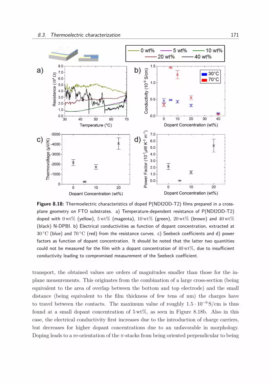
8.3. Thermoelectric characterization 171
Figure 8.18: Thermoelectric characteristics of doped P(NDI2OD-T2) films prepared in a cross-plane geometry on FTO substrates. a) Temperature-dependent resistance of P(NDI2OD-T2)doped with 0 wt% (yellow), 5 wt% (magenta), 10 wt% (green), 20 wt% (brown) and 40 wt%(black) N-DPBI. b) Electrical conductivities as function of dopant concentration, extracted at30 C (blue) and 70 C (red) from the resistance curves. c) Seebeck coefficients and d) powerfactors as function of dopant concentration. It should be noted that the latter two quantitiescould not be measured for the film with a dopant concentration of 40 wt%, due to insufficientconductivity leading to compromised measurement of the Seebeck coefficient.
transport, the obtained values are orders of magnitudes smaller than those for the in-plane measurements. This originates from the combination of a large cross-section (beingequivalent to the area of overlap between the bottom and top electrode) and the smalldistance (being equivalent to the film thickness of few tens of nm) the charges haveto travel between the contacts. The maximum value of roughly 1.5 · 10−9 S/cm is thusfound at a small dopant concentration of 5 wt%, as seen in Figure 8.18b. Also in thiscase, the electrical conductivity first increases due to the introduction of charge carriers,but decreases for higher dopant concentrations due to an unfavorable in morphology.Doping leads to a re-orientation of the π-stacks from being oriented perpendicular to being

172 Chapter 8. P(NDI2OD-T2) as n-type polymer for thermoelectric applications
oriented parallel to the substrate, which does not match with the measured direction forcharge transport, in addition to an overall loss of order.
The Seebeck coefficients of the cross-plane samples can be found in Figure 8.18c. Theyagain show the inverse trend to the electrical conductivity, with the minimal value beingfound at 5 wt% dopant concentration. For higher concentrations the Seebeck coefficientincreases again, although it cannot be determined for concentrations of 40 wt%. Thismost likely correlates to the effect of poor contacting seen for the temperature-dependentresistance curve for 40 wt% dopant. Too large resistances lead to poor contactability andthus impede the correct determination of the Seebeck coefficient and should be taken intoaccount when investigating novel systems.
As seen in Figure 8.18d, the power factor is again most strongly influenced by theevolution of the Seebeck coefficient. However, if compared to the values obtained forthe in-plane samples, the power factors found are seven orders of magnitudes smaller,with the maximum being 5 · 10−7 µWK−2m−1 at dopant concentrations of 20 wt%. Thus,it is concluded that the cross-plane geometry is not as favorable as the in-plane one,which can be explained by taking into account the morphology model. The unfavorablere-orientation of π-stacks from perpendicular to parallel, is less suitable for cross-planecharge transport.
A challenge that also arose during film fabrication, is the occurrence of short- circuitsbetween the top and the bottom electrode. Due to the low film thickness of few tens ofnanometers, it is possible for the aluminum to come directly in contact with the bottomelectrode through defects in the film, while still forming a closed layer on top. Therefore,when contacting both electrodes, short-circuits are obtained which make the measurementof resistances impossible. In order to avoid this issue, a third geometry is presented.
8.3.3 Pseudo-in-plane geometry
Finally, the third geometry investigated in this study is the newly-proposed, so-calledpseudo-in-plane geometry. This is an amalgamation of the two previously discussed ge-ometries, in that the doped P(NDI2OD-T2) film is deposited on FTO substrates. Theactive material on the FTO substrate is etched away in such a fashion that no overlapwith the thermally evaporated top aluminum electrode is obtained in the end. This leadsto macroscopic lateral distances in addition to the film thickness, which the charge car-riers have to traverse, since the electrodes do not sandwich the polymer film. The filmgeometry is also shown as inset in Figure 8.19.
The thermoelectric properties of doped P(NDI2OD-T2) films are shown in Figure 8.19.Temperature-dependent resistances are, similarly to the cross-plane investigations, on a

8.3. Thermoelectric characterization 173
Figure 8.19: Thermoelectric characteristics of doped P(NDI2OD-T2) films prepared in a pseudo-in-plane geometry on FTO substrates. a) Temperature-dependent resistance of P(NDI2OD-T2)doped with 0 wt% (yellow), 5 wt% (magenta), 10 wt% (green), 20 wt% (brown) and 40 wt%(black) N-DPBI. b) Electrical conductivities as function of dopant concentration, extracted at30 C (blue) and 70 C (red) from the resistance curves. c) Seebeck coefficients and d) powerfactors as function of dopant concentration.
similar order of magnitude. Up to concentrations of 10 wt%, a steady downward shift ofthe curves can be observed, which is then reversed for higher concentrations, as seen inFigure 8.19a.
The extracted conductivity values in Figure 8.19b again show a maximum of 0.32 S/cmat a N-DPBI concentration of 5 wt%, which is three orders of magnitude higher thanthe typical values found in the in-plane geometry. The fact that for higher dopant con-centrations the electrical conductivity again drops can again be explained by the mor-phological change induced by the doping process. The re-organization of the π-stacksand the lamellar stacking parallel to the substrate would be favorable for the pseudo-in-plane geometry, since the lateral distance is much larger than the vertical one. Thisre-orientation, however, comes at the cost of structural order within both types of stacks,

174 Chapter 8. P(NDI2OD-T2) as n-type polymer for thermoelectric applications
due to the incorporation of dopant molecules into the film. Still, the vastly improvedelectrical conductivities strengthen the feasibility of this geometry.
The Seebeck coefficients shown in Figure 8.19c show much smaller variations as functionof dopant concentration, and in general lower levels with the maximum value of roughly−470µV/K being found for the pristine sample. It should be noted at this point thatfor the in-plane geometry no Seebeck coefficient could be measured, due to the insulatingnature of pristine P(NDI2OD-T2) films. The mostly monotonous drop in Seebeck coeffi-cient with increasing amounts of N-DPBI is in agreement with UV-Vis data discussed inSection 8.1, in that higher nominal concentrations of dopant lead to larger charge carrierconcentrations.
Finally, the power factors of the pseudo-in-plane samples, seen in Figure 8.19d, show asimilar trend to that of the Seebeck coefficient. Pristine P(NDI2OD-T2) yields the max-imum value close to 2.7 µWK−2m−1, which subsequently drops for higher concentrationsof dopant. These values are easily comparable to those of the in-plane samples, discussedabove, again strengthening the feasibility of this geometry. However, the pseudo-in-planegeometry has several advantages over the in-plane one, especially regarding fabrication ofa thermoelectric generator. As discussed in the following section, when thinking of a wayof connecting p-type and n-type legs in a thermoelectric generator while trying to em-ploy an in-plane geometry, alternating deposition of the two different materials becomesdifficult. The next section will therefore deal with the conceptualization of a thermoelec-tric generator based on conducting polymers as active materials, while making use of theadvantages the pseudo-in-plane geometry provides for both the p-type PEDOT:PSS andn-type P(NDI2OD-T2) leg.
8.4 Performance of a thermoelectric generator
The main purpose of the whole investigation regarding the thermoelectric properties ofdoped P(NDI2OD-T2) is to conceptualize and fabricate a thermoelectric generator whichis solely based on conducting polymers as active materials, thus the semiconducting legs.As n-type leg the aforementioned P(NDI2OD-T2) is used, while EG-post-treated PE-DOT:PSS serves as the p-type leg in the generator. These two halves are fabricated ontop of a FTO-coated elongated glass slide, of which the central part is etched away. Afull electrical circuit is realized by the top aluminum electrode, which connects the n-typeand p-type part. It should be mentioned that for both legs, the pseudo-in-plane geometryis employed as it combines the feasible thermoelectric properties obtained in an in-planegeometry, combined with the relative ease with which the cross-plane geometry can berealized. In addition, due to the absence of overlap area between the top and bottom

8.4. Performance of a thermoelectric generator 175
electrode, the risk of device failure originating from short-circuits is greatly reduced. Asketch of the thermoelectric generator is shown in Figure 8.20, while a detailed descriptionof the fabrication process is given in Section 4.3.
Electrical contacting is ensured via the FTO electrodes located at each side of the device,while the temperatures of the ’hot’ and ’cold’ side (i.e. bottom and top) are simultane-ously monitored through placement of temperature sensors on one FTO electrode and thealuminum. A temperature gradient is measured between the electrodes. This setup leadsto temperature gradients in the range of 5 C to 7 C and allows for the comparison ofobtainable thermovoltages and I-V-characteristics of two thermoelectric generators, oneof which is built using pristine P(NDI2OD-T2) and the other with P(NDI2OD-T2) dopedwith 40 wt% N-DPBI as n-type leg. Measurements of the output voltage and the deviceresistance are shown in Figure 8.21, with the former normalized to a temperature differ-ence of 1 K. As seen in Figure 8.21a, the generator with 0 wt% P(NDI2OD-T2) shows astable output voltage of roughly 0.3 mV/K over time. Upon doping with 40 wt% N-DPBI,the output voltage is nearly tripled, leading to values around 1.1 mV/K. In both cases,the temperature gradients do not show drastic changes, as indicated by the dashed linesin Figure 8.21a.
In order to calculate the full power output P of both devices, a quantity related tothe conductivity within both generators is necessary. Therefore, the device resistancesare measured by applying different bias voltages between the two FTO electrodes andmonitoring the induced currents over time. The mean currents are then plotted against
Figure 8.20: Schematic drawing of a thermoelectric generator, employing conducting polymersas active materials. PEDOT:PSS (blue) and P(NDI2OD-T2) (turquoise) are used as p-type andn-type leg in a pseudo-in-plane geometry, respectively. Both legs are electrically connected withaluminum (gray) as top electrode, while a partially etched FTO-coated (yellow) glass slide (gray)serves as bottom electrode.

176 Chapter 8. P(NDI2OD-T2) as n-type polymer for thermoelectric applications
Figure 8.21: a) Output voltages (solid lines) and temperature differences (dashed lines), and b)I-V curves with linear fits of thermoelectric generators based on PEDOT:PSS and P(NDI2OD-T2). Two generators were studied, with dopant concentrations of 0 wt% (dark yellow) and40 wt% (black).
the respective bias voltages and yield Figure 8.21b. Since a linear relation between thevoltage and current is observed for both samples, the existence of internal resistances inthe devices can be excluded. From the slopes of the linear fits through the data pointsfor both samples, resistance (R) values can be obtained using Ohm’s law in Equation 8.1,in which U represents the bias voltage and I the induced current.
R = U
I(8.1)
The results of the characterization of both thermoelectric generators are summarizedin Figure 8.22. As discussed above, the thermovoltage is nearly tripled upon dopingwith 40 wt% from roughly 0.3 mV/K to 1.1 mV/K. In addition, the device resistance Ris reduced from 7 · 106 Ω to roughly 5 · 106 Ω. Taking both quantities into account, thepower output P can be calculated by using Equation 8.2, where U is the Voltage outputand R the device resistance.
P = U2
R(8.2)
The power output, as seen in Figure 8.22c, strongly changes upon doping. While forthe generator without dopant the power output amounts to roughly 0.2 W/K it increasesby factor 12 to average values around 2.4 W/K, resulting in largely improved power con-version capabilities.
It should be noted that one was faced with several challenges during the measurementof the full generators. One issue was the slight lateral temperature gradient, which was

8.4. Performance of a thermoelectric generator 177
Figure 8.22: a) Voltage output, b) conductance and c) power output for two thermoelectric gen-erators, with dopant concentrations of 0 wt% (dark yellow) and 40 wt% (black). d) Photographsof the investigated generators, with the n-type leg always being on the right side.
induced due to the asymmetric setup in XAVER. Specifically, the hot copper block wasplaced centered underneath the Al-bridge on the generator. This inevitably led to slightlydifferent temperatures between both FTO electrodes. Additionally, this lateral temper-ature gradient was enhanced by the presence of water in the cold copper block, whichwas situated underneath one of the FTO electrodes. As it turns out, the effect of thecold copper block on the lateral gradient is diminished, once the former is emptied ofwater. It can be argued that the water in the cold copper block acts as heat sink, andthus causes the asymmetry in the temperature distribution along the device. In presenceof water, the lateral temperature gradient amounts to roughly 3 C to 7 C, while in theformer’s absence a gradient of barely 1 C is measured. These issues can potentially besolved through further improvement of XAVER. Still, the discussion of the fabricationand implementation of polymer-based thermoelectric generators up to this point servesas proof-of-concept of the design.

178 Chapter 8. P(NDI2OD-T2) as n-type polymer for thermoelectric applications
In summary, the implementation of the pseudo-in-plane geometry allowed for the facilefabrication of thermoelectric generators based on the conducting polymers PEDOT:PSSand P(NDI2OD-T2) as active materials. Doping of the n-type component with N-DPBIgreatly improves the voltage output, while also reducing the internal device resistance.The combination of both factors leads to a twelve-fold improvement in power output,rendering the design, choice of components and doping promising approaches for thermalenergy conversion using thermoelectric generators.
8.5 Summary
In this chapter, the n-type polymer P(NDI2OD-T2) is investigated regarding its thermo-electric capabilities. N-DPBI is used as dopant molecule, in order to introduce chargesinto the system, allowing for the investigation of changes upon addition of the former.
UV-Vis spectroscopy was used to study the changes on an electronic level. Additionof dopant into the polymer solution prior to film fabrication lead to the decrease of thecharacteristic absorption bands from the polymer, while bands assigned to the presenceof polaronic states appear. This makes UV-Vis spectroscopy a viable tool for the confir-mation of successful doping. Degradation as function of temperature and exposure timein air is also studied, indicating that temperatures above 80 C accelerate the degradationprocess through reaction of the doped films with atmospheric oxygen.
The morphological changes upon doping of P(NDI2OD-T2) were studied using GI-WAXS. In the pristine state, the polymer forms π-stacks in vertical direction, which ex-tend along the polymer backbone and lead to the formation of lamellae. Macroscopically,these lamellar stacks form crystallites which preferably orient in a face-on manner. Upondoping, N-DPBI molecules are increasingly incorporated into the π-stacks, destroyingthe order within. The addition of dopant also leads to re-orientation the lamellar stack-ing, from being oriented primarily parallel to the substrate, to being primarily orientedperpendicular to the substrate. As a consequence, the crystallites built up by lamellarstacking change their orientation from face- to edge-on.
Lastly, the findings of the spectroscopic and morphological investigations are linked withthe thermoelectric properties of doped P(NDI2OD-T2) films. Different possible geome-tries for the implementation of P(NDI2OD-T2) in thermoelectric generators are proposedand investigated regarding temperature-dependent resistances, electrical conductivities,Seebeck coefficients and power factors as function of concentration. The in-plane geom-etry combines high Seebeck coefficients with moderate electrical conductivities, yieldingmaximum power factors of 2.7 µWK-2m−1, which is on the same order of magnitude asfor highly conducting PEDOT:PSS films. The cross-plane geometry suffers from very

8.5. Summary 179
low electrical conductivities, therefore strongly limiting the power conversion capabilities.In addition, the risk of short-circuiting due to defects in the film is greatly increaseddue to the overlap between the bottom FTO and top aluminum electrode. Thus, thepseudo-in-plane geometry is offered as alternative, in which there is no overlap betweenthe aforementioned electrodes. This geometry is also advantageous due to moderatelyhigh Seebeck coefficients in the range of hundreds of microvolts per Kelvin, while improv-ing the electrical conductivities even beyond those obtained for the in-plane geometry. Itis thus deemed most viable for the fabrication of thermoelectric generators, into whichEG-treated PEDOT:PSS as p-type component is added.
The thermoelectric generators are studied with respect to their output voltage, overalldevice resistance and power output, comparing a generator with pristine P(NDI2OD-T2)to one in which P(NDI2OD-T2) is doped with 40 wt% N-DPBI. Doping leads to a threefoldimproved output voltage, decreased device resistance and thus twelvefold increased poweroutput of the generator. It should be highlighted that all measurements were performedon a single generator with one p-n-pair. In principle, the adopted sample geometry allowsfor facile connection of several generators together, in order to increase the absolute poweroutput.


9 Conclusion and outlook
The main focus of the present thesis is the investigation of conducting polymers withrespect to their potential thermoelectric capabilities and the elucidation of links betweenthe structure and the performance. As the field of organic thermoelectrics is still quiteyoung, this work aims at the understanding of the underlying concepts and if knowledgegained with inorganic thermoelectrics can be extended to these systems. Therefore, eachchapter of this thesis focuses on the directed modification of a thermoelectric parameter,in order to link the thermoelectric properties of a polymer thin film to its structure.
Nanostructuring of PEDOT:PSS thin films is successfully achieved through the inclu-sion of Si-NPs. TOF-GISANS is used for the elucidation of a suitable fabrication protocol,resulting in the layer-by-layer fabrication for the composite films for further investigations.In order to understand the impact of the latters’ inclusion on thermoelectric properties,and specifically on the thermal conductivity, IRT is employed. It is revealed that, apartfrom the other relevant thermoelectric parameters, the thermal conductivity is indeedmodified. Due to the single-crystalline nature of the Si-NPs, the thermal conductivity in-creases for small concentrations and subsequently drops. An explanation for this behavioris found with the aid of GIR-TeXS, which allows for clear distinction of the individualcomponents in the ternary PEDOT:PSS/Si-NPs hybrid composite films, due to theirmolecular structure. In this specific case, the nanostructuring approach proved to be suc-cessful, since GIR-TeXS revealed the selective incorporation of Si-NPs into PEDOT-richdomains, instead of the PSS-rich matrix, with the former being mostly responsible forthe measurable thermoelectric properties. The presence of Si-NPs disturbs the internalorder of the domains and subsequently leads to less efficient heat transport within thefilm, similarly to nanostructuring in inorganic thermoelectric materials.
A high intrinsic charge carrier concentration in the PEDOT:PSS PH1000 formulationis responsible for the observation of potentially high electrical conductivities in thin films,but comes at the cost of low Seebeck coefficients. It is seen that through appropriatechoice of treatment agents in the form of inorganic salts with either acido-basic or redoxproperties, the doping level can be modified. This dedoping yields increased Seebeckcoefficients and simultaneously decreased electrical conductivities, supporting a loss ofcharge carriers during the process. Both UV-Vis spectroscopy and XPS additionally
181

182 Chapter 9. Conclusion and outlook
reveal changes in the electronic structure. With Raman spectroscopy it becomes possibleto link the loss in electrical conductivity with changes in the conformation of PEDOTthrough the transition from the quinoid form of PEDOT to the benzoid form. Mostimportantly, this transition occurs irrespective of the mechanism by which PEDOT:PSSis dedoped. Regarding redox dedoping, the choice of agent is not critical, as only theabsolute number of reducing equivalents interacting with PEDOT determine the finalthermoelectric properties of the thin film.
PEDOT:PSS is a binary polymer blend, in which positively charged PEDOT chainsinteract electrostatically with negatively charged PSS chains. Not only does PSS stabilizethe positive charges on PEDOT chains, but it also influences the final morphology of thinfilms prepared from the polymer blend. One possible way to simultaneously enhance boththe Seebeck coefficient and electrical conductivity is to employ ILs, which complementthe binary nature of PEDOT:PSS. Through post-treatment of PEDOT:PSS thin films notonly the degree of doping is changed, but also the structure of the thin film. The rationalchoice of ILs in this study serves a dual purpose. Variation of the anion, while keeping thesame cation allows for a closer study of the impact of the anions’ properties on the finalthermoelectric properties. EMIM DCA yielded the highest Seebeck coefficients, followedby EMIM BF4 and EMIM TCB. These observations are mostly assigned to the abilityof the negative charge on the anions to interact with the positively charged PEDOT.Additionally, the interaction between the positively charged EMIM cations and the neg-atively charged PSS anions is also altered through variation of the ILs’ anions, resultingin different structures through secondary doping and improved electrical conductivities.Thus, post-treatment of PEDOT:PSS with ILs enables the simultaneous enhancementof both Seebeck coefficient and electrical conductivity through a combination of primaryand secondary doping. The large library of anion-cation combinations in ILs additionallyopens a large window for the tunability of thermoelectric properties in PEDOT:PSS.
Lastly, in order to complement PEDOT:PSS as a p-type organic thermoelectric mate-rial, P(NDI2OD-T2) is investigated regarding its suitability upon doping with N-DPBI.Successful transfer of negative charge carriers onto the polymer is confirmed through UV-Vis spectroscopy through the emergence of polaronic bands. This also sheds light on aninherent challenge regarding doped n-type polymers, which is their susceptibility towardsdegradation in ambient atmosphere. The impact of doping on the structure is also evi-dent from GIWAXS measurements indicating re-orientation and a loss of order within inthe polymer with increasing amount of dopant. Finally, different geometries of thermo-electric thin films from doped P(NDI2OD-T2) are investigated regarding their suitabilityin a thermoelectric generator, with the in-plane and pseudo-in-plane showing the mostpromise. A link between the observations from the spectroscopic and structural investi-

183
gations to the thermoelectric properties is found in the trends for the Seebeck coefficientand electrical conductivity as function of dopant concentration. Doped P(NDI2OD-T2) isthen used in conjunction with PEDOT:PSS in order to build a thermoelectric generatorbased on conducting polymers as active materials, proving the feasibility of the employedapproach.
For future research, it will be interesting to have a closer look at other material systemsand their potential thermoelectric capabilities. While PEDOT:PSS is a very good ref-erence system, it has some intrinsic disadvantages like its two-component nature, whichproves detrimental in some aspects. P(NDI2OD-T2) on the other hand suffers from com-paratively low electrical conductivity, motivating the search for a material system whichcombines the advantages of the investigated polymers. Also the aspect of implementationinto devices and large-scale applications is worth pursuing further, as the potential inenergy recovery is significant.

Bibliography
[1] L. D. Hicks and M. S. Dresselhaus, “Thermoelectric Figure of Merit of a One-Dimensional Conductor,” Physical Review B, vol. 47, no. 24, 1993.
[2] N. Saxena, M. Coric, A. Greppmair, J. Wernecke, M. Pfluger, M. Krumrey, M. S.Brandt, E. M. Herzig, and P. Muller-Buschbaum, “Morphology-Function Rela-tionship of Thermoelectric Nanocomposite Films from PEDOT:PSS with SiliconNanoparticles,” Advanced Electronic Materials, vol. 3, no. 8, p. 1700181, 2017.
[3] N. Saxena, J. Keilhofer, A. K. Maurya, G. Fortunato, J. Overbeck, and P. Muller-Buschbaum, “Facile Optimization of Thermoelectric Properties in PEDOT:PSS ThinFilms through Acido-Base and Redox Dedoping Using Readily Available Salts,” ACSApplied Energy Materials, vol. 1, no. 2, pp. 336–342, 2018.
[4] N. Saxena, B. Pretzl, X. Lamprecht, L. Bießmann, D. Yang, N. Li, C. Bilko, S. Bern-storff, and P. Muller-Buschbaum, “Ionic liquids as Post-Treatment Agents for Si-multaneous Improvement of Seebeck Coefficient and Electrical Conductivity in PE-DOT:PSS Films,” ACS Applied Materials & Interfaces, vol. 11, pp. 8060–8071, 2019.
[5] L. Onsager, “Reciprocal Relations in Irreversible Processes. I,” Physical Review,vol. 37, no. 4, pp. 405–426, 1931.
[6] H. J. Goldsmid, Introduction to Thermoelectricity, vol. 121. Springer, 2 ed., 2011.[7] G. J. Snyder and E. S. Toberer, “Complex Thermoelectric Materials,” Nature Mate-
rials, vol. 7, no. 2, pp. 105–114, 2008.[8] R. Kroon, D. A. Mengistie, D. Kiefer, J. Hynynen, J. D. Ryan, L. Yu, and C. Muller,
“Thermoelectric Plastics: From Design to Synthesis, Processing and Structure-Property Relationships,” Chemical Society Reviews, vol. 45, no. 22, pp. 6147–6164,2016.
[9] W. P. Su, J. R. Schrieffer, and A. J. Heeger, “Solitons in Polyacetylene,” PhysicalReview Letters, vol. 42, no. 25, 1979.
[10] W. P. Su, J. R. Schrieffer, and A. J. Heeger, “Soliton Excitations in Polyacetylene,”Physical Review B, vol. 22, no. 4, 1980.
[11] J. T. Devreese, “Polarons,” vol. 14 of Encyclopedia of Applied Physics, pp. 383–409,Wiley-VCH Publishers, Inc., 1996.
185

186 Bibliography
[12] A. Elschner, S. Kirchmeyer, W. Lovenich, U. Merker, and K. Reuter, PEDOT: Prin-ciples and Applications of an Intrinsically Conductive Polymer. Boca Raton: CRCPress, Taylor & Francis Group, 2011.
[13] H. Park, S. H. Lee, F. S. Kim, H. H. Choi, I. W. Cheong, and J. H. Kim, “Enhancedthermoelectric properties of PEDOT: PSS nanofilms by a chemical dedoping process,”Journal of Materials Chemistry A, vol. 2, no. 18, pp. 6532–6539, 2014.
[14] T. Takano, H. Masunaga, A. Fujiwara, H. Okuzaki, and T. Sasaki, “PEDOTNanocrystal in Highly Conductive PEDOT: PSS Polymer Films,” Macromolecules,vol. 45, no. 9, pp. 3859–3865, 2012.
[15] A. M. Nardes, M. Kemerink, M. M. de Kok, E. Vinken, K. Maturova, and R. Janssen,“Conductivity, Work Function, and Environmental Stability of PEDOT:PSS ThinFilms Treated with Sorbitol,” Organic Electronics, vol. 9, no. 5, pp. 727–734, 2008.
[16] Y. Yoneda, “Anomalous Surface Reflection of X Rays,” Physical Review, vol. 131,no. 5, 1963.
[17] B. L. Henke, E. M. Gullikson, and J. C. Davis, “X-ray interactions: photoabsorption,scattering, transmission and reflection at E = 50-30000 eV, Z = 1-92,” Atomic Dataand Nuclear Data Tables, no. 54, 1993.
[18] G. Renaud, R. Lazzari, and F. Leroy, “Probing Surface and Interface Morphologywith Grazing Incidence Small Angle X-Ray Scattering,” Surface Science Reports,vol. 64, no. 8, pp. 255–380, 2009.
[19] A. Hexemer and P. Muller-Buschbaum, “Advanced Grazing-Incidence Techniquesfor Modern Soft-Matter Materials Analysis,” International Union of CrystallographyJournal, vol. 2, no. Pt 1, pp. 106–125, 2015.
[20] P. Muller-Buschbaum, “Grazing incidence small-angle X-ray scattering: an advancedscattering technique for the investigation of nanostructured polymer films,” Analyti-cal and Bioanalytical Chemistry, vol. 376, no. 1, pp. 3–10, 2003.
[21] R. Lazzari, “IsGISAXS: A Program for Grazing-Incidence Small-Angle X-ray Scat-tering Analysis of Supported Islands,” Journal of Applied Crystallography, vol. 35,2002.
[22] R. L. Kronig, “On the Theory of Dispersion of X-Rays,” Journal of the Optical SocietyAmerica, vol. 12, no. 6, pp. 547–558, 1926.
[23] J. L. Baker, L. H. Jimison, S. Mannsfeld, S. Volkman, S. Yin, V. Subramanian,A. Salleo, A. P. Alivisatos, and M. F. Toney, “Quantification of Thin Film Crystal-lographic Orientation Using X-Ray Diffraction with an Area Detector,” Langmuir,vol. 26, no. 11, pp. 9146–9151, 2010.

Bibliography 187
[24] X. Lamprecht, Influence of Ionic Liquids on Thermoelectric Properties of PolymerThin Films and Design of a New Seebeck Coefficient Measurement Setup. Bachelor’sthesis, Technical University Munich, 2016.
[25] R. Kluge, Investigation of an n-Type Polymer for Thermoelectric Applications. Mas-ter’s thesis, Technical University Munich, 2017.
[26] A. Greppmair, B. Stoib, N. Saxena, C. Gerstberger, P. Muller-Buschbaum, M. Stutz-mann, and M. S. Brandt, “Measurement of the In-Plane Thermal Conductivityby Steady-State Infrared Thermography,” Review of Scientific Instruments, vol. 88,no. 4, p. 044903, 2017.
[27] M. Krumrey and G. Ulm, “High-Accuracy Detector Calibration at the PTB Four-Crystal Monochromator Beamline,” Nuclear Instruments and Methods in PhysicsResearch Section A: Accelerators, Spectrometers, Detectors and Associated Equip-ment, vol. 467-468, pp. 1175–1178, 2001.
[28] C. A. Schneider, W. S. Rasband, and K. W. Eliceiri, “NIH Image to ImageJ: 25 Yearsof Image Analysis,” Nature Methods, vol. 9, no. 7, pp. 671–675, 2012.
[29] Z. Jiang, “GIXSGUI: A MATLAB Toolbox for Grazing-Incidence X-Ray Scatter-ing Data Visualization and Reduction, and Indexing of Buried Three-DimensionalPeriodic Nanostructured Films,” Journal of Applied Crystallography, vol. 48, no. 3,pp. 917–926, 2015.
[30] J. Fink, E. Schierle, E. Weschke, and J. Geck, “Resonant Elastic Soft X-Ray Scat-tering,” Reports on Progress in Physics, vol. 76, no. 5, p. 056502, 2013.
[31] J. Wernecke, C. Gollwitzer, P. Muller, and M. Krumrey, “Characterization of an In-Vacuum PILATUS 1M Detector,” Journal of Synchrotron Radiation, vol. 21, no. Pt3, pp. 529–536, 2014.
[32] R. Kampmann, M. Haese-Seiller, V. Kudryashov, V. Deriglazov, M. Tristl, C. Daniel,B. Toperverg, A. Schreyer, and E. Sackmann, “The Potential of the Horizontal Re-flectometer REFSANS/FRM-II for Measuring Low Reflectivity and Diffuse SurfaceScattering,” Physica B: Condensed Matter, vol. 350, no. 1-3, pp. E763–E766, 2004.
[33] P. Muller-Buschbaum, “Grazing Incidence Small-Angle Neutron Scattering: Chal-lenges and possibilities,” Polymer Journal, vol. 45, no. 1, pp. 34–42, 2013.
[34] G. Schierning, J. Stoetzel, R. Chavez, V. Kessler, J. Hall, R. Schmechel, T. Schnei-der, N. Petermann, H. Wiggers, S. Angst, D. E. Wolf, B. Stoib, A. Greppmair,M. Stutzmann, and M. S. Brandt, “Silicon-Based Nanocomposites for Thermoelec-tric Application,” physica status solidi (a), vol. 213, no. 3, pp. 497–514, 2016.

188 Bibliography
[35] P. Muller-Buschbaum, “Influence of Surface Cleaning on Dewetting of ThinPolystyrene Films,” The European Physical Journal. E, Soft Matter, vol. 12, no. 3,pp. 443–448, 2003.
[36] F. Greco, A. Zucca, S. Taccola, A. Menciassi, T. Fujie, H. Haniuda, S. Takeoka,P. Dario, and V. Mattoli, “Ultra-Thin Conductive Free-Standing PEDOT:PSSNanofilms,” Soft Matter, vol. 7, no. 22, p. 10642, 2011.
[37] G. J. Snyder and E. S. Toberer, “Complex Thermoelectric Materials,” Nature Mate-rials, vol. 7, no. 2, pp. 105–114, 2008.
[38] C. B. Vining, “The Thermoelectric Limit ZT˜1: Fact or Artifact,” Proceedings of the10th International Conference on Thermoelectrics, vol. 10, 1992.
[39] S. K. Yee, N. E. Coates, A. Majumdar, J. J. Urban, and R. A. Segalman, “Thermo-electric Power Factor Optimization in PEDOT:PSS Tellurium Nanowire Hybrid Com-posites,” Physical Chemistry Chemical Physics : PCCP, vol. 15, no. 11, pp. 4024–4032, 2013.
[40] E. J. Bae, Y. H. Kang, K.-S. Jang, and S. Y. Cho, “Enhancement of Thermoelec-tric Properties of PEDOT:PSS and Tellurium-PEDOT:PSS Hybrid Composites bySimple Chemical Treatment,” Scientific Reports, vol. 6, p. 18805, 2016.
[41] C. M. Palumbiny, J. Schlipf, A. Hexemer, C. Wang, and P. Muller-Buschbaum, “TheMorphological Power of Soap: How Surfactants Lower the Sheet Resistance of PE-DOT:PSS by Strong Impact on Inner Film Structure and Molecular Interface Orien-tation,” Advanced Electronic Materials, vol. 2, no. 4, p. 1500377, 2016.
[42] S. Niesar, R. N. Pereira, A. R. Stegner, N. Erhard, M. Hoeb, A. Baumer, H. Wiggers,M. S. Brandt, and M. Stutzmann, “Low-Cost Post-Growth Treatments of CrystallineSilicon Nanoparticles Improving Surface and Electronic Properties,” Advanced Func-tional Materials, vol. 22, no. 6, pp. 1190–1198, 2012.
[43] L. Bießmann, L. P. Kreuzer, T. Widmann, N. Hohn, J.-F. Moulin, and P. Muller-Buschbaum, “Monitoring the Swelling Behavior of PEDOT:PSS Electrodes underHigh Humidity Conditions,” ACS Applied Materials & Interfaces, vol. 10, no. 11,pp. 9865–9872, 2018.
[44] J. Chen, T. Sun, D. Sim, H. Peng, H. Wang, S. Fan, H. H. Hng, J. Ma, F. Y. C.Boey, S. Li, M. K. Samani, G. C. K. Chen, X. Chen, T. Wu, and Q. Yan, “Sb2Te3Nanoparticles with Enhanced Seebeck Coefficient and Low Thermal Conductivity,”Chemistry of Materials, vol. 22, no. 10, pp. 3086–3092, 2010.
[45] J. Liu, X. Wang, D. Li, N. E. Coates, R. A. Segalman, and D. G. Cahill, “ThermalConductivity and Elastic Constants of PEDOT: PSS with High Electrical Conduc-tivity,” Macromolecules, vol. 48, no. 3, pp. 585–591, 2015.

Bibliography 189
[46] D. G. Cahill, “Thermal Conductivity Measurement from 30 to 750 K: The 3wMethod,” Review of Scientific Instruments, vol. 61, no. 2, pp. 802–808, 1990.
[47] G. Kaune, M. A. Ruderer, E. Metwalli, W. Wang, S. Couet, K. Schlage, R. Rohls-berger, S. V. Roth, and P. Muller-Buschbaum, “In Situ GISAXS Study of Gold FilmGrowth on Conducting Polymer Films,” ACS Applied Materials & Interfaces, vol. 1,no. 2, pp. 353–360, 2009.
[48] Q. Wei, C. Uehara, M. Mukaida, K. Kirihara, and T. Ishida, “Measurement ofIn-Plane Thermal Conductivity in Polymer Films,” AIP Advances, vol. 6, no. 4,p. 045315, 2016.
[49] M. A. Vairavamurthy, D. Maletic, S. Wang, B. Manowitz, T. Eglinton, and T. Lyons,“Characterization of Sulfur-Containing Functional Groups in Sedimentary HumicSubstances by X-ray Absorption Near-Edge Structure Spectroscopy,” Energy & Fu-els, vol. 11, no. 3, pp. 546–553, 1997.
[50] J. Keilhofer, Enhancement of thermoelectric properties of PEDOT:PSS by redox dop-ing and acid-base doping. Bachelor’s thesis, Technical University Munich, 2017.
[51] A. K. Maurya, Optimization of the thermoelectric properties of conducting polymerthin films by dedoping and hybrid approaches. PhD thesis, Technical University Mu-nich, 2016.
[52] M. N. Gueye, A. Carella, N. Massonnet, E. Yvenou, S. Brenet, J. Faure-Vincent,S. Pouget, F. Rieutord, H. Okuno, A. Benayad, R. Demadrille, and J.-P. Simonato,“Structure and Dopant Engineering in PEDOT Thin Films: Practical Tools fora Dramatic Conductivity Enhancement,” Chemistry of Materials, vol. 28, no. 10,pp. 3462–3468, 2016.
[53] H. Shi, C. Liu, Q. Jiang, and J. Xu, “Effective Approaches to Improve the ElectricalConductivity of PEDOT: PSS: A Review,” Advanced Electronic Materials, vol. 1,no. 4, p. 1500017, 2015.
[54] O. Bubnova, Z. U. Khan, H. Wang, S. Braun, D. R. Evans, M. Fabretto, P. Hojati-Talemi, D. Dagnelund, J.-B. Arlin, Y. H. Geerts, S. Desbief, D. W. Breiby, J. W.Andreasen, R. Lazzaroni, W. M. Chen, I. Zozoulenko, M. Fahlman, P. J. Murphy,M. Berggren, and X. Crispin, “Semi-Metallic Polymers,” Nature Materials, vol. 13,no. 2, pp. 190–194, 2014.
[55] Z. Fan, P. Li, D. Du, and J. Ouyang, “Significantly Enhanced Thermoelectric Proper-ties of PEDOT: PSS Films through Sequential Post-Treatments with Common Acidsand Bases,” Advanced Energy Materials, vol. 7, no. 8, p. 1602116, 2017.
[56] N. Massonnet, A. Carella, O. Jaudouin, P. Rannou, G. Laval, C. Celle, and J.-P. Simonato, “Improvement of the Seebeck Coefficient of PEDOT:PSS by Chemical

190 Bibliography
Reduction Combined with a Novel Method for its Transfer Using Free-Standing ThinFilms,” Journal of Materials Chemistry C, vol. 2, no. 7, pp. 1278–1283, 2014.
[57] M. Stavytska-Barba and A. M. Kelley, “Surface-Enhanced Raman Study of the In-teraction of PEDOT: PSS with Plasmonically Active Nanoparticles,” The Journal ofPhysical Chemistry C, vol. 114, no. 14, pp. 6822–6830, 2010.
[58] Q. Wei, M. Mukaida, Y. Naitoh, and T. Ishida, “Morphological Change and Mo-bility Enhancement in PEDOT:PSS by Adding Co-Solvents,” Advanced Materials(Deerfield Beach, Fla.), vol. 25, no. 20, pp. 2831–2836, 2013.
[59] C. Yi, A. Wilhite, L. Zhang, R. Hu, S. S. C. Chuang, J. Zheng,and X. Gong, “Enhanced Thermoelectric Properties of Poly(3,4-ethylenedioxythiophene):poly(styrenesulfonate) by Binary Secondary Dopants,”ACS Applied Materials & Interfaces, vol. 7, no. 17, pp. 8984–8989, 2015.
[60] Z. Zhu, C. Liu, Q. Jiang, H. Shi, F. Jiang, J. Xu, J. Xiong, and E. Liu, “Opti-mizing the Thermoelectric Properties of PEDOT:PSS Films by Combining OrganicCo-Solvents with Inorganic Base,” Journal of Materials Science: Materials in Elec-tronics, vol. 26, no. 11, pp. 8515–8521, 2015.
[61] Z. Fan, D. Du, Z. Yu, P. Li, Y. Xia, and J. Ouyang, “Significant Enhancement in theThermoelectric Properties of PEDOT:PSS Films through a Treatment with OrganicSolutions of Inorganic Salts,” ACS Applied Materials & Interfaces, vol. 8, no. 35,pp. 23204–23211, 2016.
[62] C. Yeon, S. J. Yun, J. Kim, and J. W. Lim, “PEDOT: PSS Films with GreatlyEnhanced Conductivity via Nitric Acid Treatment at Room Temperature and TheirApplication as Pt/TCO-Free Counter Electrodes in Dye-Sensitized Solar Cells,” Ad-vanced Electronic Materials, vol. 1, no. 10, p. 1500121, 2015.
[63] Z. U. Khan, O. Bubnova, M. J. Jafari, R. Brooke, X. Liu, R. Gabrielsson, T. Ederth,D. R. Evans, J. W. Andreasen, M. Fahlman, and X. Crispin, “Acido-Basic Con-trol of the Thermoelectric Properties of Poly(3,4-ethylenedioxythiophene)tosylate(PEDOT-Tos) Thin Films,” Journal of materials chemistry. C, Materials for opticaland electronic devices, vol. 3, no. 40, pp. 10616–10623, 2015.
[64] S. R. S. Kumar, N. Kurra, and H. N. Alshareef, “Enhanced High Temperature Ther-moelectric Response of Sulphuric Acid Treated Conducting Polymer Thin Films,”Journal of Materials Chemistry C, vol. 4, no. 1, pp. 215–221, 2016.
[65] J. Ouyang, “Solution-Processed PEDOT:PSS Films with Conductivities as IndiumTin Oxide through a Treatment with Mild and Weak Organic Acids,” ACS AppliedMaterials & Interfaces, vol. 5, no. 24, pp. 13082–13088, 2013.

Bibliography 191
[66] C. M. Palumbiny, C. Heller, C. J. Schaffer, V. Korstgens, G. Santoro, S. V. Roth,and P. Muller-Buschbaum, “Molecular Reorientation and Structural Changes inCosolvent-Treated Highly Conductive PEDOT: PSS Electrodes for Flexible IndiumTin Oxide-Free Organic Electronics,” The Journal of Physical Chemistry C, vol. 118,no. 25, pp. 13598–13606, 2014.
[67] K. van de Ruit, I. Katsouras, D. Bollen, T. van Mol, R. A. J. Janssen, D. M. de Leeuw,and M. Kemerink, “The Curious Out-of-Plane Conductivity of PEDOT: PSS,” Ad-vanced Functional Materials, vol. 23, no. 46, pp. 5787–5793, 2013.
[68] O. Bubnova, Z. U. Khan, A. Malti, S. Braun, M. Fahlman, M. Berggren, andX. Crispin, “Optimization of the thermoelectric figure of merit in the conducting poly-mer poly(3,4-ethylenedioxythiophene),” Nature Materials, vol. 10, no. 6, pp. 429–433,2011.
[69] C. Badre, L. Marquant, A. M. Alsayed, and L. A. Hough, “Highly ConductivePoly(3,4-ethylenedioxythiophene): Poly (styrenesulfonate) Films Using 1-Ethyl-3-methylimidazolium Tetracyanoborate Ionic Liquid,” Advanced Functional Materials,vol. 22, no. 13, pp. 2723–2727, 2012.
[70] R. J. Murphy, K. M. Weigandt, D. Uhrig, A. Alsayed, C. Badre, L. Hough,and M. Muthukumar, “Scattering Studies on Poly(3,4-ethylenedioxythiophene)–Polystyrenesulfonate in the Presence of Ionic Liquids,” Macromolecules, vol. 48,no. 24, pp. 8989–8997, 2015.
[71] A. d. Izarra, S. Park, J. Lee, Y. Lansac, and Y. H. Jang, “Ionic Liquid Designedfor PEDOT:PSS Conductivity Enhancement,” Journal of the American ChemicalSociety, vol. 140, no. 16, pp. 5375–5384, 2018.
[72] S. Kee, N. Kim, B. S. Kim, S. Park, Y. H. Jang, S. H. Lee, J. Kim, J. Kim, S. Kwon,and K. Lee, “Controlling Molecular Ordering in Aqueous Conducting Polymers UsingIonic Liquids,” Advanced Materials (Deerfield Beach, Fla.), vol. 28, no. 39, pp. 8625–8631, 2016.
[73] Z. Fan, D. Du, X. Guan, and J. Ouyang, “Polymer films with ultrahigh thermo-electric properties arising from significant seebeck coefficient enhancement by ionaccumulation on surface,” Nano Energy, vol. 51, pp. 481–488, 2018.
[74] H. Wang, D. Zhao, Z. U. Khan, S. Puzinas, M. P. Jonsson, M. Berggren, andX. Crispin, “Ionic Thermoelectric Figure of Merit for Charging of Supercapacitors,”Advanced Electronic Materials, vol. 3, no. 4, p. 1700013, 2017.
[75] S. Spange, R. Lungwitz, and A. Schade, “Correlation of molecular structure andpolarity of ionic liquids,” Journal of Molecular Liquids, vol. 192, pp. 137–143, 2014.
192 Bibliography
[76] A. M. Nardes, M. Kemerink, R. A. J. Janssen, J. A. M. Bastiaansen, N. M. M.Kiggen, B. M. W. Langeveld, van Breemen, A. J. J. M., and M. M. de Kok, “Micro-scopic Understanding of the Anisotropic Conductivity of PEDOT: PSS Thin Films,”Advanced Materials (Deerfield Beach, Fla.), vol. 19, no. 9, pp. 1196–1200, 2007.
[77] P. Wei, J. H. Oh, G. Dong, and Z. Bao, “Use of a 1H-Benzoimidazole Derivative asan n-Type Dopant and to Enable Air-Stable Solution-Processed n-Channel OrganicThin-Film Transistors,” Journal of the American Chemical Society, vol. 132, no. 26,pp. 8852–8853, 2010.
[78] R. Steyrleuthner, M. Schubert, I. Howard, B. Klaumunzer, K. Schilling, Z. Chen,P. Saalfrank, F. Laquai, A. Facchetti, and D. Neher, “Aggregation in a High-Mobilityn-Type Low-Bandgap Copolymer with Implications on Semicrystalline Morphology,”Journal of the American Chemical Society, vol. 134, no. 44, pp. 18303–18317, 2012.
[79] M. Caironi, M. Bird, D. Fazzi, Z. Chen, R. Di Pietro, C. Newman, A. Facchetti,and H. Sirringhaus, “Very Low Degree of Energetic Disorder as the Origin of HighMobility in an n-channel Polymer Semiconductor,” Advanced Functional Materials,vol. 21, no. 17, pp. 3371–3381, 2011.
[80] J. Rivnay, R. Steyrleuthner, L. H. Jimison, A. Casadei, Z. Chen, M. F. Toney, A. Fac-chetti, D. Neher, and A. Salleo, “Drastic Control of Texture in a High Performancen-Type Polymeric Semiconductor and Implications for Charge Transport,” Macro-molecules, vol. 44, no. 13, pp. 5246–5255, 2011.
[81] E. Giussani, D. Fazzi, L. Brambilla, M. Caironi, and C. Castiglioni, “MolecularLevel Investigation of the Film Structure of a High Electron Mobility Copolymer viaVibrational Spectroscopy,” Macromolecules, vol. 46, no. 7, pp. 2658–2670, 2013.
[82] E. Giussani, L. Brambilla, D. Fazzi, M. Sommer, N. Kayunkid, M. Brinkmann,and C. Castiglioni, “Structural Characterization of Highly Oriented Naphthalene-Diimide-Bithiophene Copolymer Films via Vibrational Spectroscopy,” Journal ofPhysical Chemistry B, vol. 119, no. 5, pp. 2062–2073, 2015.
[83] A. M. Anton, R. Steyrleuthner, W. Kossack, D. Neher, and F. Kremer, “InfraredTransition Moment Orientational Analysis on the Structural Organization of theDistinct Molecular Subunits in Thin Layers of a High Mobility n-Type Copolymer,”Journal of the American Chemical Society, vol. 137, no. 18, pp. 6034–6043, 2015.
[84] T. Schuettfort, S. Huettner, S. Lilliu, J. E. Macdonald, L. Thomsen, and C. R.McNeill, “Surface and Bulk Structural Characterization of a High-Mobility Electron-Transporting Polymer,” Macromolecules, vol. 44, no. 6, pp. 1530–1539, 2011.
[85] T. Schuettfort, L. Thomsen, and C. R. McNeill, “Observation of a Distinct Surface

Bibliography 193
Molecular Orientation in Films of a High Mobility Conjugated Polymer,” Journal ofthe American Chemical Society, vol. 135, no. 3, pp. 1092–1101, 2013.
[86] A. M. Anton, R. Steyrleuthner, W. Kossack, D. Neher, and F. Kremer, “Spatial Ori-entation and Order of Structure-Defining Subunits in Thin Films of a High Mobilityn-Type Copolymer,” Macromolecules, vol. 49, no. 5, pp. 1798–1806, 2016.
[87] R. Steyrleuthner, R. Di Pietro, B. A. Collins, F. Polzer, S. Himmelberger, M. Schu-bert, Z. Chen, S. Zhang, A. Salleo, H. Ade, A. Facchetti, and D. Neher, “The Roleof Regioregularity, Crystallinity, and Chain Orientation on Electron Transport ina High-Mobility n-Type Copolymer,” Journal of the American Chemical Society,vol. 136, no. 11, pp. 4245–4256, 2014.
[88] M. Brinkmann, E. Gonthier, S. Bogen, K. Tremel, S. Ludwigs, M. Hufnagel, andM. Sommer, “Segregated versus mixed interchain stacking in highly oriented films ofnaphthalene diimide bithiophene copolymers,” ACS Nano, vol. 6, no. 11, pp. 10319–10326, 2012.
[89] A. M. Anton, R. Steyrleuthner, W. Kossack, D. Neher, and F. Kremer, “Spatial Ori-entation and Order of Structure-Defining Subunits in Thin Films of a High Mobilityn-Type Copolymer,” Macromolecules, vol. 49, no. 5, pp. 1798–1806, 2016.
[90] R. A. Schlitz, F. G. Brunetti, A. M. Glaudell, P. L. Miller, M. A. Brady, C. J. Takacs,C. J. Hawker, and M. L. Chabinyc, “Solubility-Limited Extrinsic n-Type Dopingof a High Electron Mobility Polymer for Thermoelectric Applications,” AdvancedMaterials (Deerfield Beach, Fla.), vol. 26, no. 18, pp. 2825–2830, 2014.


List of publications
Publications related to the dissertation
• N. Saxena, M. Coric, A. Greppmair, M. Pfluger, M. Krumrey, M. S. Brandt, E.M. Herzig, P. Muller-Buschbaum, ”Morphology-Function Relationship of Thermo-electric Nanocomposite Films from PEDOT:PSS with Silicon Nanoparticles”, Adv.Electron. Mater., vol. 3, pp. 1700181 – 1700195, 2017.
• N. Saxena, J. Keilhofer, A. K. Maurya, G. Fortunato, J. Overbeck, P. Muller-Buschbaum, ”Facile Optimization of Thermoelectric Properties in PEDOT:PSSThin Films through Acido-Base and Redox Dedoping Using Readily Available Salts”,ACS Appl. Energy Mater., vol. 1, pp. 336-342, 2018.
• N. Saxena, B. Pretzl, X. Lamprecht, L. Bießmann, D. Yang, N. Li, C. Bilko, S.Bernstorff, P. Muller-Buschbaum, ”Ionic Liquids as Post-Treatment Agents for Si-multaneous Improvement of Seebeck Coefficient and Electrical Conductivity in PE-DOT:PSS Films”, ACS Appl. Mater. Interfaces, just accepted.
• A. Greppmair, B. Stoib, N. Saxena, C. Gerstberger, P. Muller-Buschbaum, M.Stutzmann, M.S. Brandt, ”Measurement of the In-Plane Thermal Conductivity bySteady-State Infrared Thermography”, Rev. Sci. Instr., vol. 88, pp. 044903, 2017.
Further publications
• M. Coric, N. Saxena, M. Pfluger, P. Muller-Buschbaum, M. Krumrey, E. M. Herzig,”Resonant Grazing-Incidence Small-Angle X-Ray Scattering at the Sulfur K-Edgefor Material-Specific Investigation of Thin Film Nanostructures, J. Phys. Chem.Lett., vol. 9, pp. 3081-3086, 2018.
• B. Su, H. A. Caller-Guzman, V. Korstgens, Y. Rui, Y. Yao, N. Saxena, G. Santoro,S.V. Roth, P. Muller-Buschbaum, ”Macro-Scale and Nano-Scale Morphology Evo-lution during In-Situ Spray Coating of Titania Films for Perovskite Solar Cells”,ACS Appl. Mater. Interfaces, vol. 9, pp. 43724-43732, 2017.
195

196 List of publications
• L. Song, T. Wang, V. Korstgens, W. Wang, N. Saxena, C. J. Schaffer, T. Froschl,N. Husing, S. Bernstorff, P. Muller-Buschbaum, ”Wet-Imprinting of Channel-TypeSuperstructures in Nanostructured Titania Thin Films at Low Temperatures forHybrid Solar Cells”, ChemSusChem, vol. 11, pp. 1179-1186, 2018.
• L. Bießmann, N. Saxena, N. Hohn, M. A. Hossain, J. G. C. Veinot, P. Muller-Buschbaum, ”Highly Conducting, Transparent PEDOT:PSS Polymer Electrodesfrom Post-Treatment with Weak and Strong Acids”, Adv. Electron. Mater., vol. 5,pp. 1800654 – 180664, 2019.
• N. Hohn, A. E. Hetzenecker, M. A. Giebel, S. Geier, L. Bießmann, V. Korstgens,N. Saxena, J. Schlipf, W. Ohm, P. S. Deimel, F. Allegretti, J. V. Barth, S. V. Roth,T. F. Fassler, P. Muller-Buschbaum, ”Amphiphilic Diblock Copolymer-MediatedStructure Control in Nanoporous Germanium-Based Thin Films, Nanoscale, vol.11, pp. 2048-2055, 2019.
Scientific reports
• N. Saxena, A. Greppmair, M. Coric, J. Wernecke, S. Marggraf, E. M. Herzig,M. S. Brandt, P. Muller-Buschbaum, ”Hybrid Thermoelectrics Based on a Polymer-Nanoparticle Composite”, Lehrstuhl fur Funktionelle Materialien, Annual Report,2014.
• N. Saxena, A. Greppmair, M. S. Brandt, P. Muller-Buschbaum, ”Full Thermoelec-tric Characterization of Highly Conducting PEDOT:PSS Thin Films”, Lehrstuhl furFunktionelle Materialien, Annual Report, 2015.
• A. K. Maurya, N. Saxena, P. Muller-Buschbaum, ”Optimization of ThermoelectricProperties of PEDOT:PSS Thin Films through a Dedoping Approach”, Lehrstuhlfur Funktionelle Materialien, Annual Report, 2016.
• N. Saxena, M. Coric, A. Greppmair, J. Wernecke, M. Pfluger, M. Krumrey, M.S. Brandt, E. M. Herzig, P. Muller-Buschbaum, ”Morphology-Function Relation-ship in Thermoelectric Nanocomposites from PEDOT:PSS with Inorganic SiliconNanoparticles”, Lehrstuhl fur Funktionelle Materialien, Annual Report, 2017.
• P. Muller-Buschbaum, ”Full Thermoelectric Characterization of Highly ConductingPEDOT:PSS Thin Films”, CeNS Annual Report, 2016.
• N. Saxena, J. Schlipf, L. Bießmann, D. Moseguı Gonzalez, S. Bernstorff, P. Muller-Buschbaum, ”In-Operando GISAXS and GIWAXS on Novel Thermoelectric Com-posite Films”, Elettra Annual Report, 2015.

List of publications 197
Conference talks
• N. Saxena, A. Greppmair, F. Baumer, T. Nilges, M. S. Brandt, P. Muller-Buschbaum,”Hybrid thermoelectrics based on conducting polymers”, MSE Colloquium, Garch-ing, Germany, 2015.
• N. Saxena, M. Coric, A. Greppmair, J. Wernecke, S. Langner, M. Krumrey, M. S.Brandt, E. M. Herzig, P. Muller-Buschbaum, ”Thermoelectric thin films based on apolymer/nanoparticle nanocomposite”, DPG Frujahrstagung, Regensburg, 2016.
• N. Saxena, M. Coric, A. Greppmair, J. Wernecke, M. Pluger, M. Krumrey, M. S.Brandt, E. M. Herzig, P. Muller-Buschbaum, ”Thermoelectric thin films based on apolymer/nanoparticle nanocomposite”, DPG-Fruhjahrstagung, Dresden, 2017.
• N. Saxena, M. Coric, A. Greppmair, J. Wernecke, M. Pluger, M. Krumrey, M. S.Brandt, E. M. Herzig, P. Muller-Buschbaum, ”Thermoelectric thin films based ona polymer/nanoparticle nanocomposite”, 3rd Internal Biennial Science Meeting ofthe MLZ, Grainau, 2017.
• N. Saxena, M. Coric, A. Greppmair, J. Wernecke, M. Pluger, M. Krumrey, M. S.Brandt, E. M. Herzig, P. Muller-Buschbaum, ”Thermoelectric thin films based ona polymer/nanoparticle nanocomposite”, European Polymer Federation Congress,Lyon, 2017.
• N. Saxena, M. Coric, A. Greppmair, J. Wernecke, M. Pluger, M. Krumrey, M. S.Brandt, E. M. Herzig, P. Muller-Buschbaum, ”Thermoelectric thin films based on apolymer/nanoparticle nanocomposite”, textitZhejiang Sci-Tech University, Hangzhou,China, 2017,
• N. Saxena, B. Pretzl, X. Lamprecht, D. Yang, N. Li, C. Bilko, S. Bernstorff, P.Muller-Buschbaum, ”Ionic Liquid Post-Treatment of PEDOT:PSS Thin Films forImprovement of Thermoelectric Properties”, DPG-Fruhjahrstagung, Berlin, 2018.
Conference poster presentations
• N. Saxena, A. Greppmair, M. S. Brandt, P. Muller-Buschbaum, ”Novel nanostruc-tured thermoelectric hybrid materials”, MSE Colloquium 2014, Garching, 2014.
• N. Saxena, A. Greppmair, M. Coric, J. Wernecke, S. Marggraf, E. M. Herzig, M.S. Brandt, P. Muller-Buschbaum, ”Novel thermoelectric films based on a polymer-nanoparticle composite”, CeNS Workshop ”‘Walk and talk on the nanoscale”’, 2014.
• N. Saxena, A. Greppmair, M. S. Brandt, P. Muller-Buschbaum, ”Thermoelektrika:Strom aus Warme”, NIM Nanoday, Munich, 2014.
198 List of publications
• N. Saxena, A. Greppmair, M. S. Brandt, P. Muller-Buschbaum, ”Novel thermoelec-tric films based on a polymer-nanoparticle composite”, DPG Spring meeting 2014,Berlin, 2015.
• N. Saxena, A. Greppmair, M. S. Brandt, P. Muller-Buschbaum, ”Novel thermoelec-tric films based on a polymer-nanoparticle composite”, Summer School, Grainau,2015.
• N. Saxena, A. Greppmair, M. S. Brandt, P. Muller-Buschbaum, ”Novel thermo-electric films based on a polymer-nanoparticle composite”, Congress of EuropeanPolymer Federation, Dresden, 2015.
• N. Saxena, M. Coric, J. Wernecke, S. Langner, M. Krumrey, E. M. Herzig, P. Muller-Buschbaum, ”Hybrid thermoelectrics based on a polymer/nanoparticle composite”,SAS 2015, Berlin, 2015.
• N. Saxena, M. Philipp, L. Song, C. M. Palumbiny, M. Haese-Seiller, J.-F. Moulin,P. Muller-Buschbaum, ”Hybrid thermoelectrics based on a polymer/nanoparticlecomposite”, Julich Center for Neutron Science Workshop, Tutzing, 2015.
• N. Saxena, M. Coric, A. Greppmair, J. Wernecke, S. Langner, M. Krumrey, M. S.Brandt, E. M. Herzig, P. Muller-Buschbaum, ”Hybrid thermoelectrics based on apolymer/nanoparticle composite”, 5th SolarTech International Conference in Mu-nich, 2016.
• N. Saxena, M. Coric, A. Greppmair, J. Wernecke, S. Langner, M. Krumrey, M. S.Brandt, E. M. Herzig, P. Muller-Buschbaum, ”Hybrid thermoelectrics based on apolymer/nanoparticle composite”, MSE Colloquium 2016, Munich, 2016.
• N. Saxena, M. Coric, A. Greppmair, J. Wernecke, S. Langner, M. Krumrey, M. S.Brandt, E. M. Herzig, P. Muller-Buschbaum, ”Hybrid thermoelectrics based on apolymer/nanoparticle composite”, Summer School CEA-TUM ’Future of commoneuropean energy strategy’, Frauenchiemsee, 2016.
• N. Saxena, M. Coric, A. Greppmair, J. Wernecke, M. Pfluger, S. Langner, M. Krum-rey, M. S. Brandt, E. M. Herzig, P. Muller-Buschbaum, ”Tender resonant x-ray scat-tering (T-ReXS) on polymer/nanoparticle hybrid thermoelectrics”, GISAXS Work-shop 2016, Hamburg, 2016.
• N. Saxena, M. Coric, A. Greppmair, J. Wernecke, M. Pluger, M. Krumrey, M. S.Brandt, E. M. Herzig, P. Muller-Buschbaum, ”Thermoelectric thin films based on apolymer/nanoparticle nanocomposite”, NIM Young Ideas in Nanoscience, Munich,2017.
• N. Saxena, M. Coric, A. Greppmair, J. Wernecke, M. Pluger, M. Krumrey, M. S.Brandt, E. M. Herzig, P. Muller-Buschbaum, ”Thermoelectric thin films based on

List of publications 199
a polymer/nanoparticle nanocomposite”, Munich School of Engineering Colloquium2017 , 2017.
• N. Saxena, M. Coric, A. Greppmair, J. Wernecke, M. Pluger, M. Krumrey, M. S.Brandt, E. M. Herzig, P. Muller-Buschbaum, ”Thermoelectric thin films based on apolymer/nanoparticle nanocomposite”, NIM Nanostructured Functional Materialsfor Sustainable Energy Provision, Munich, 2017.
• N. Saxena, M. Coric, A. Greppmair, J. Wernecke, M. Pluger, M. Krumrey, M. S.Brandt, E. M. Herzig, P. Muller-Buschbaum, ”Thermoelectric thin films based on apolymer/nanoparticle nanocomposite”, NIM ’The Future of Nanoscience’, Tutzing,2018.
• N. Saxena, M. Coric, A. Greppmair, J. Wernecke, M. Pluger, M. Krumrey, M.S. Brandt, E. M. Herzig, P. Muller-Buschbaum, ”Thermoelectric thin films basedon a polymer/nanoparticle nanocomposite”, German Conference for Research withSynchrotron Radiation, Neutrons and Ion Beams at Large-Scale Facilities, Garching,2018.


Acknowledgments
In my time as PhD student at the TUM, I made many valuable experiences. For that Iowe many people, who I would like to acknowledge at the end of my thesis.
First and foremost, I would like to thank my supervisor Prof. Dr. Peter Muller-Buschbaum for allowing me to join the Chair of Functional Materials, his guidance when-ever it was needed, and also for challenging me with the interesting topic of organicthermoelectrics. His drive to send us out to conferences, workshops and meetings, and ingeneral becoming part of the scientific community has enriched my PhD experience, forwhich I am grateful. His belief in my abilities, as well as his letting me come up with myown ideas and see them come to fruition has strongly shaped my experience.
This work is the product of many fruitful collaborations, which were also largely sup-ported by the MSE seed funding project ’Novel Nanostructured Thermoelectric HybridMaterials’. Our cooperation with Prof. Martin S. Brandt and Dr. Anton Greppmair onthe measurement of thermal conductivity of polymer thin films, and deep discussions onthe physics of organic thermoelectrics were some of the highlights of my work. Addition-ally, I want to thank Prof. Dr. Eva M. Herzig and especially Mihael Coric for the infinitetenacity while tackling the resonant scattering beast, from which I have also benefited.Dr. Krumrey, Dr. Jan Wernecke and Mika Pfluger also receive my thanks for their sup-port with the resonant scattering measurements and challenging evaluation of the data.Dr. Giuseppino Fortunato and Jan Overbeck are also gratefully acknowledged for theirgreat help with X-ray photoelectron spectroscopy and Raman spectroscopy, in my timeof need.
My work at the Chair for Functional Materials has allowed me to dive into the worldof research at large-scale facilities for the first time in my career. Therefore, I want toacknowledge the team from the MiNaXS-beamline at the DESY, Hamburg, led by Prof.Dr. Stephan Roth, along with Dr. Matthias Schwartzkopf, Calvin Brett, Marc Gensch,Dr. Wiebke Ohm, Sven-Jannik Wohnert, Jan Rubeck and Dr. Pallavi Pandit. I hadgreat times at the MiNaXS-beamlines, but also at several workshops and conferences.Dr. Sigrid Bernstorff is acknowledged for her support during beamtimes at the AustrianSAXS beamline at the Elettra Sincrotrone Trieste. I would also like to thank Dr. Jean-
201

202 List of publications
Francois Moulin and Martin Haese-Seiller for the TOF-GISANS measurements at theREFSANS-beamline at the FRM II, Garching.
Both the Nanosystems Initiative Munich (NIM) and the Center for Nanoscience (CeNS)receive my thanks for creating such great environments in their graduate programs. Espe-cially, I would like to thank Dr. Peter Sonntag, Dr. Birgit Ziller, Silke Mayerl-Kink, Dr.Isabella Almstatter for organizing many great events, and also Criss Hohmann for designof cover pictures. I thank Prof. Dr. Christine Papadakis for taking over my mentorship.
You guys went under many different names, ’Thermoelectric Workforce’, my ’slaves’,my ’kiddies’: Regina Kluge, Anjani Kumar Maurya, Xaver Lamprecht, Mike J. Jost,Mubashar Rafiq, Benjamin Pretzl, Josef ’Seppi’ Keilhofer, Benedikt Fuchs, Paul Steinacker,as well as my NIM summer research students Robin Tyburski and Haider Haseeb. As mystudents you had such a positive impact on my work at the Chair that I can barely putit into words. Having been your advisor on your individual paths on becoming scientistshas really enriched me. Not only did I learn about teaching and understanding others,but I have also learned a lot about myself. Large parts of this thesis only exist becauseof your hard work, accuracy and motivation. I hope that you learned as much from me,as I did from you. I am really grateful that all of you were part of this journey, and wishyou guys all the best for your future!
The Chair for Functional Materials will always hold a special place in my heart.Through tough times, through relaxed times, through fun times, it was always the mem-bers of the Chair who kept me coming into the office with a smile on my face everysingle day. This is why I want to thank Johannes Schlipf, Lorenz Bießmann, Nuri Hohn,Franziska Lohrer, Daniel Mosegui Gonzalez, Mihael Coric, Jenny Lebert, Stephan Proller,Oliver Filonik, Volker Korstgens, Lucas Kreuzer, Tobias Widmann, Sebastian Grott, Si-mon Schaper, Shambhavi Pratap as well as our ’new’ generation, Kerstin Wienhold,Julian Heger, Christina Geiger, Lennart Reb, Roy Schaffrinna, Dominik Schwaiger andAnna-Lena Oechsle from the bottom of my heart. I will always fondly remember our’escalations/ just one beer’s’ at Schwasi, Rennbahn, Hopfendolde, etc., Karaoke nightsat Kennedy’s, exciting and exhausting DPG spring meetings, occasional late shifts atuniversity, beamtimes aided by refrigerating animals, hair straighteners and Celine Dion,workshops, BBQ’s, etc.
Our colleagues from China, especially Lin Song, Bo Su, Senlin Xia, Ray Wang, KunWang, Dan Yang, Qi Zhong, Wei Chen, Wei Cao, Xiaohan Zhang, Xinyu Jiang, Nian Li,Shanshan Yin, are gratefully acknowledged for giving me interesting insights into chineseculture.
Thank you also to Bart-Jan Niebuur, Chia-Hsin Ko, Florian Jung and Jia-Jhen Kangfor always enduring seminar talks on photovoltaics.

In the beginning, our ’alumni’ took me in and helped to make my first months at thechair very pleasant. For that I want to thank Kuhu Sarkar, Markus Schindler, ShuaiGuo, David Magerl, Claudia Palumbiny, Yuan Yao, Weijia Wang, Margarita Dyakonova,Christoph J. Schaffer, Natalya Vishnevetskaya, Martine Philipp, Konstantinos Raftopou-los, Anatoly Berezkin, Ezzeldin Metwalli, as well as our master students, SebastianGunther, Christoph Mayr, Michael Bahr, Rosa Torrademe-Torrademe, Lukas Oesinghaus,Edoardo Barabino, Richard Stockhausen, May Kaeppel, Kiran Mathew John, ChristophSenfter, Thomas Kaps, Bernhard Springer, Bernhard Kalis, Gilles Mohl, Fabien Guelle,Andreas Hetzenecker, Steffen Schlosser, Christoph Bilko, Raphael Markl and ChristianWeindl.
Big thank you also to Susanna Fink, Marion Waletzki, Carola Kappauf and DieterMuller for keeping things running silently in the background, and for their help againstthe bureaucracy monster. Another big thank you to Reinhold Funer, Nick Schroder,Sebastian Fink, as well as Manfred Pfaller and his team from the central workshop, whoall helped with the building of XAVER. Michael Bohmler, Terry Weinmann and EgonLenker are gratefully acknowledged for their support regarding everything electronics-related.
Another great thing about my time as a PhD student was the formation of the PolymerMusic Band, in several line-ups over the years. Here, I want to specifically acknowledgeJohannes Schlipf, Claudia Palumbiny, Christoph Schaffer, Eva M. Herzig, Susanna Fink,Jenny Lebert, Michael Bahr, Simon Schaper, Lucas Kreuzer, Wei Chen, Regina Kluge,Gilles Mohl, Fabien Guelle, Shambhavi Pratap, Chia-Hsin Ko, Julian Heger and ChristinaGeiger. We had lots of amazing gigs, and I am very proud to call myself the drummer ofthe Polymer Music Band!
Lastly, I want to thank my family and friends for their unconditional support, bothmental and emotional. My friends from old times, school times and university times havealways helped me getting even through tough times. Especially my parents, my sister,my brother-in-law and my little nephews have been a source of energy and motivationespecially in this challenging last period of my work. I am also very grateful for theiroccasional pushes and motivational speeches when I was not living up to my own ex-pectations. Without you, none of this would have been possible. Therefore, I want todedicate this work to you!