In situ studies of strain dependent transport properties of conducting polymers on elastomeric...
7
In situ studies of strain dependent transport properties of conducting polymers on elastomeric substrates Venugopalan Vijay, Arun D. Rao, and K. S. Narayan Citation: Journal of Applied Physics 109, 084525 (2011); doi: 10.1063/1.3580514 View online: http://dx.doi.org/10.1063/1.3580514 View Table of Contents: http://scitation.aip.org/content/aip/journal/jap/109/8?ver=pdfcov Published by the AIP Publishing Articles you may be interested in Highly clear conductive polymer electrode films hybridized with gold nanoparticles Appl. Phys. Lett. 99, 233304 (2011); 10.1063/1.3665612 Structure and properties of polymer core-shell systems: Helium ion microscopy and electrical conductivity studies J. Vac. Sci. Technol. B 28, C6P59 (2010); 10.1116/1.3504589 Direct observation of localized conduction pathways in photocross-linkable polymer memory J. Appl. Phys. 105, 124516 (2009); 10.1063/1.3153980 Conducting Ni nanoparticles in an ion-modified polymer J. Appl. Phys. 98, 066101 (2005); 10.1063/1.2014938 X-ray photoemission spectroscopy studies of conducting polymer-substrate interfaces: Interfacial electrochemical diffusion J. Appl. Phys. 81, 7313 (1997); 10.1063/1.365353 [This article is copyrighted as indicated in the article. Reuse of AIP content is subject to the terms at: http://scitation.aip.org/termsconditions. Downloaded to ] IP: 203.200.35.19 On: Wed, 29 Apr 2015 11:15:35
Transcript of In situ studies of strain dependent transport properties of conducting polymers on elastomeric...
In situ studies of strain dependent transport properties of conducting polymers onelastomeric substratesVenugopalan Vijay, Arun D. Rao, and K. S. Narayan Citation: Journal of Applied Physics 109, 084525 (2011); doi: 10.1063/1.3580514 View online: http://dx.doi.org/10.1063/1.3580514 View Table of Contents: http://scitation.aip.org/content/aip/journal/jap/109/8?ver=pdfcov Published by the AIP Publishing Articles you may be interested in Highly clear conductive polymer electrode films hybridized with gold nanoparticles Appl. Phys. Lett. 99, 233304 (2011); 10.1063/1.3665612 Structure and properties of polymer core-shell systems: Helium ion microscopy and electrical conductivity studies J. Vac. Sci. Technol. B 28, C6P59 (2010); 10.1116/1.3504589 Direct observation of localized conduction pathways in photocross-linkable polymer memory J. Appl. Phys. 105, 124516 (2009); 10.1063/1.3153980 Conducting Ni nanoparticles in an ion-modified polymer J. Appl. Phys. 98, 066101 (2005); 10.1063/1.2014938 X-ray photoemission spectroscopy studies of conducting polymer-substrate interfaces: Interfacial electrochemicaldiffusion J. Appl. Phys. 81, 7313 (1997); 10.1063/1.365353
[This article is copyrighted as indicated in the article. Reuse of AIP content is subject to the terms at: http://scitation.aip.org/termsconditions. Downloaded to ] IP:
203.200.35.19 On: Wed, 29 Apr 2015 11:15:35
In situ studies of strain dependent transport properties of conductingpolymers on elastomeric substrates
Venugopalan Vijay, Arun D. Rao, and K. S. Narayana)
Jawaharlal Nehru Centre of Advanced Scientific Research, Jakkur P.O., Bangalore-560064, India
(Received 18 December 2010; accepted 16 March 2011; published online 28 April 2011)
We report the changes in the surface electrical resistance, R, of conducting polymer, Poly
(3,4-ethylenedioxythiophene)-poly(styrenesulfonate) (PEDOT:PSS) films coated on appropriate
flexible substrates in stretched conditions. These studies are important in the context of flexible
organic electronic applications. In situ conductivity measurements on pristine PEDOT:PSS thin
films on elastomeric substrates upon stretching reveal a minima in R as a function of strain, x, prior
to the expected increase at higher strain levels. The studies emphasize (i) role of substrates,
(ii) stress-induced anisotropic features, and temperature dependence of R (iii) in comparison of R(x)
in polymer films to that of conventional metal films. The stress induced changes is modeled in terms
of effective medium approximation. VC 2011 American Institute of Physics. [doi:10.1063/1.3580514]
I. INTRODUCTION
Organic electronics based devices have been pursued in
energy,1,2 display,3,4 and sensor5,6 related applications. The
polymeric nature of the active electronic component and the
possibility of fabricating devices on soft substrates open up a
whole range of sensors that can be integrated to our surround-
ings. The additional possibility of incorporating stretching and
bending capabilities of such products introduces valuable fea-
tures that can be incorporated in novel design concepts.3–6
Substantial efforts have been taken toward this direction in the
recent past.1–8 An essential aspect in the development of the
next generation of flexible devices is the prerequisite knowl-
edge of microscopic aspects of the changes in the structure
and associated electrical transport as a function of the me-
chanical parameters.
Flexibility, a combination of bending and stretching, can
lead to deterioration of both the polymer bulk and electrode
electronic properties along with changes in the mechanical
integrity of the active layers, interfaces, and substrates.9,10
Stretching studies of blend composites consisting of conduct-
ing polymer incorporated in polyurethanes have demon-
strated flexible electrode characteristics.11 However, there
are no reports related to layered-stretchable composite struc-
tures. Critical components in these devices are the conformal
substrates, which have the right combination of surface fea-
tures, optical, and mechanical properties. Besides the novelty
aspect of flexible devices, there are considerable advantages
in the device fabrication and processing conditions upon
introduction of such substrates. A possible candidate for
such a substrate is the styrene ethylene butadiene styrene tri-
block copolymer (SEBS). SEBS elastomer obtained from
Kraton Polymers G1721M, (having a tensile stress of �2
MPa and the elongation break at 200% strain) is traditionally
used in footwear and engineering plastic applications as syn-
thetic replacements for rubber, specifically due to properties
such as flexibility, high traction, and sealing abilities, with
increased resistance to heat, weathering, and chemicals.
We focus on PEDOT:PSS as a representative conducting
polymer for the active layer. PEDOT:PSS is a technologically
important polymer and is an active component in light emit-
ting diodes,12,13 field effect transistors,14–16 solar cells,17–19
and sensors and plays the role of electrodes or electron block-
ing/hole injecting layers.20 Thin films of PEDOT:PSS are
formed from an aqueous suspension on various rigid or plastic
substrates.21–24 The conducting form of PEDOT:PSS avail-
able as exhibits a conductivity r of 460 6 20 S/cm and a work
function of 5.35 6 0.05 eV. Conductivity of 460 6 20 S/cm
corresponds to a surface resistance (R) value of 140 6 4 0 X/
h which is close to the obtained value in our laboratory of
325 6 70 X/h. However, all elastic substrates are not typi-
cally amenable for solution deposited film formation with
PEDOT:PSS thin films binding well to only those elastic sub-
strates that undergo appropriate substrate-processing proce-
dures in presence of adhesion promoters. Our work primarily
focuses on the studies of electrical transport properties of
PEDOT:PSS films upon deforming the elastomeric substrates.
The mechanical response of the conducting polymer blend
film as the substrates strain, are difficult to track closely,
unlike the electrical response, which can be monitored contin-
uously. Straining basically modifies the surface and the bulk
morphologies, which in turn results in changes of the electri-
cal macroscopic parameters such as the electrode-series resist-
ance. We report specifically the stress induced changes in
PEDOT:PSS thin films coated on SEBS substrates. Interest-
ingly, optical quality PEDOT:PSS film not only maintained
its mechanical integrity in the stretched conditions but exhib-
ited enhancement in electrical conductivity, r, in the stretched
direction over a limited range of strain. However, a decrease
in r was observed in the direction perpendicular to strain,
leading to a strain induced anisotropy. The influence of the
substrate deformation on PEDOT:PSS is unlike that of
changes in conventional metal films where the crack and
defect propagation is clearly observed beyond small threshold
strains. It is well known that for nonhardened free standing
a)Author to whom correspondence should be addressed. Electronic mail:
0021-8979/2011/109(8)/084525/6/$30.00 VC 2011 American Institute of Physics109, 084525-1
JOURNAL OF APPLIED PHYSICS 109, 084525 (2011)
[This article is copyrighted as indicated in the article. Reuse of AIP content is subject to the terms at: http://scitation.aip.org/termsconditions. Downloaded to ] IP:
203.200.35.19 On: Wed, 29 Apr 2015 11:15:35
films, the instabilities from the tensile deformation promote
the film to thin down locally (necking instability) to result in a
rupture. The length scales for the elongation are expectedly in
the order of the film thickness. In case of metal bonded to the
substrate, the strain field is delocalized, and the rupture strain
magnitude exceeds in comparison to the rupture strain of the
free standing film. The stress profile has been speculated to
arise from a formation of multiple necking locations.25,26 It
has been observed that when a metallic film/polymer bilayer
is mechanically loaded, electrical failure likely occurs well
before mechanical collapse because the formation of micro-
cracks on the film surface is more disruptive for the electrical
conductance.27,28 There is no analogous model for defect
propagation in conducting polymer blends adhered to an elas-
tomeric substrate. A model of differential effective medium
approximation is then adapted to explain the nature of the con-
ductivity observables upon straining, which in our case con-
siders electric field scattering from conducting grains
embedded in a matrix.
II. EXPERIMENTAL SETUP AND PROCEDURE
Styrene ethylene butadiene styrene (SEBS) was pro-
cured from Kraton Polymers (G1721M) in pellet form, and
flexible substrate films were obtained in a controlled manner
by solution processing using chloroform as a solvent. The
aqueous dispersion of PEDOT:PSS (Agfa, Orgacon Printing
Ink EL - P3040) was spin coated on SEBS films of 32� 18
mm substrate films at 2000 rpm (30 s), and post annealing
(70 �C for 12 hr) films of �120 nm thickness were obtained.
Gold deposition on all flexible substrates was done using
standard thermal vapor deposition procedure under high vac-
uum conditions.
The setup for stretching and bending was a home-built
arrangement powered by a two stage stepper motor. Bending
of the samples was done by keeping the samples between two
incoming blockades, which bend the sample symmetrically,
and the contacts were taken out from the edges of the samples
[Fig. 5(a)]. For stretching, the film is clamped at two ends and
uni-axially stretched as seen from Fig. 2(a). The free standing
PEDOT:PSS-coated SEBS films were stretched in a controlled
manner for a minimum of two stretch cycles. The electrical
probe assembly consisted of gold-coated neodymium-iron-bo-
ron magnets [two columns of square faced magnets (12 mm)
separated by a distance of 6 mm] and a counter magnetic base
providing the self-alignment required for the studies. The re-
sistance measurements were done at desired stretched ratios.
The arrangement consisted of Au-coated magnetic probes on
an arm that can be gradually introduced on the film along with
a counter magnetic plate on the other side of the film that pro-
vided the support and the alignment [Fig. 2(a) schematic].
The base magnetic plate–magnet interaction enabled accurate
positioning of the electrodes on the same region at different
stretching ratios. The base-magnet interaction contact
strengths where adjusted to a magnitude so as to minimize
any variation in the resistance values. The probe induced
stress was kept to a minimal level, and the integrity of the film
surface was maintained during the course of measurements.
The conductance values using this arrangement were in close
agreement with four-probe measurements using standard
thermally evaporated Au-coated electrodes for unstretched
samples, indicating negligible contact resistance in the mea-
surement setup. It is to be noted that the stretching/straining
was done with the probe arm lifted off, and successive meas-
urements are taken by placing the probes on the strained film at
the same spatial position.
III. RESULTS AND DISCUSSION
Variety of substrates including SEBS, PDMS, PMMA,
and natural and nitrile rubbers were used to deposit
PEDOT:PSS films. Uniform films were obtained on these
substrates using appropriate processing conditions. A mild
strain (2� 5%) of the substrate, however, resulted in a cer-
tain degree of nonuniformity and inhomogeneities in the film
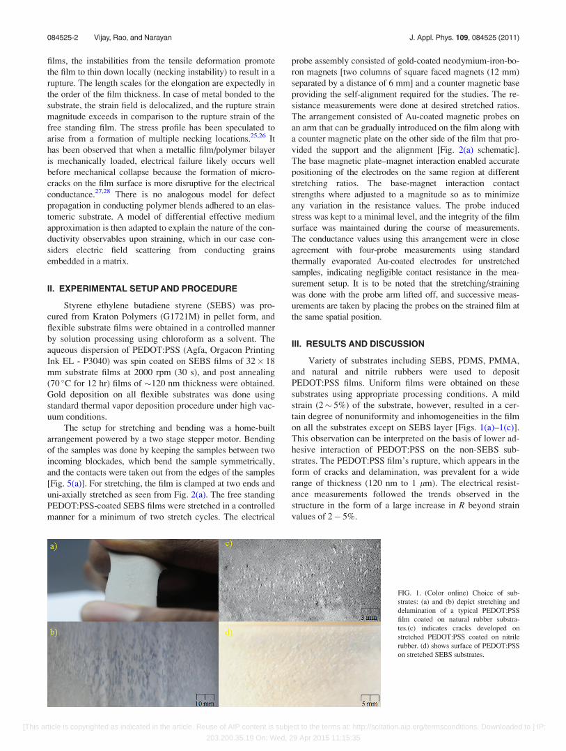
on all the substrates except on SEBS layer [Figs. 1(a)–1(c)].
This observation can be interpreted on the basis of lower ad-
hesive interaction of PEDOT:PSS on the non-SEBS sub-
strates. The PEDOT:PSS film’s rupture, which appears in the
form of cracks and delamination, was prevalent for a wide
range of thickness (120 nm to 1 lm). The electrical resist-
ance measurements followed the trends observed in the
structure in the form of a large increase in R beyond strain
values of 2� 5%.
FIG. 1. (Color online) Choice of sub-
strates: (a) and (b) depict stretching and
delamination of a typical PEDOT:PSS
film coated on natural rubber substra-
tes.(c) indicates cracks developed on
stretched PEDOT:PSS coated on nitrile
rubber. (d) shows surface of PEDOT:PSS
on stretched SEBS substrates.
084525-2 Vijay, Rao, and Narayan J. Appl. Phys. 109, 084525 (2011)
[This article is copyrighted as indicated in the article. Reuse of AIP content is subject to the terms at: http://scitation.aip.org/termsconditions. Downloaded to ] IP:
203.200.35.19 On: Wed, 29 Apr 2015 11:15:35
In case of SEBS substrates (thickness: �1 mm), the
PEDOT:PSS films were able to maintain their integrity over
a wider range of strain [Fig. 1(d)]. The textured surface of
SEBS creates local fluctuations in surface energy and contact
area; this promotes the adhesion of PEDOT:PSS films to sub-
strates through van der Waals interactions. Moreover, the
addition of ethanol, ethylene glycol, and other surfactants to
PEDOT:PSS dispersion decreases the polymer substrate
interfacial tension and provides better binding capabilities.
The surface of PEDOT:PSS films on strained/unstrained
SEBS were quite uniform. SEM and atomic force micros-
copy (AFM) studies on pristine samples showed no indica-
tions of any preferred orientation. r was also measured along
different directions on the film surface prior to stretching.
The surface r did not exhibit any signs of anisotropy, and
the magnitude did not have any directional dependence. The
absence of inhomogeneities on the semitransparent
PEDOT:PSS surface is seen in Fig. 1(d). SEM studies on
nonstretched and the stretched samples (up to 20% strain)
did not reveal any apparent surface discontinuities, cracks, or
signs of delamination in the micrometer regime of the
PEDOT:PSS film. Discernible features between the stretched
and the unstretched films were also not present in the higher
magnification SEM and AFM observations.
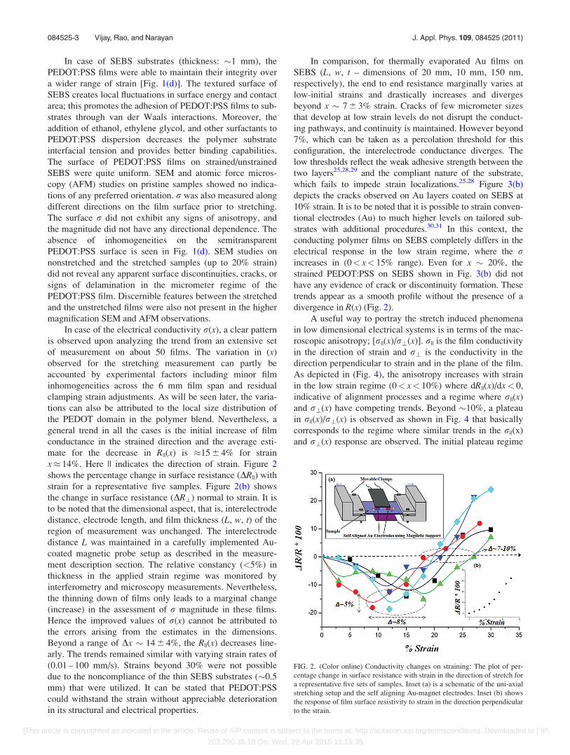
In case of the electrical conductivity r(x), a clear pattern
is observed upon analyzing the trend from an extensive set
of measurement on about 50 films. The variation in (x)
observed for the stretching measurement can partly be
accounted by experimental factors including minor film
inhomogeneities across the 6 mm film span and residual
clamping strain adjustments. As will be seen later, the varia-
tions can also be attributed to the local size distribution of
the PEDOT domain in the polymer blend. Nevertheless, a
general trend in all the cases is the initial increase of film
conductance in the strained direction and the average esti-
mate for the decrease in R||(x) is �15 6 4% for strain
x� 14%. Here || indicates the direction of strain. Figure 2
shows the percentage change in surface resistance (DR||) with
strain for a representative five samples. Figure 2(b) shows
the change in surface resistance (DR\) normal to strain. It is
to be noted that the dimensional aspect, that is, interelectrode
distance, electrode length, and film thickness (L, w, t) of the
region of measurement was unchanged. The interelectrode
distance L was maintained in a carefully implemented Au-
coated magnetic probe setup as described in the measure-
ment description section. The relative constancy (<5%) in
thickness in the applied strain regime was monitored by
interferometry and microscopy measurements. Nevertheless,
the thinning down of films only leads to a marginal change
(increase) in the assessment of r magnitude in these films.
Hence the improved values of r(x) cannot be attributed to
the errors arising from the estimates in the dimensions.
Beyond a range of Dx � 14 6 4%, the R||(x) decreases line-
arly. The trends remained similar with varying strain rates of
(0.01 – 100 mm/s). Strains beyond 30% were not possible
due to the noncompliance of the thin SEBS substrates (�0.5
mm) that were utilized. It can be stated that PEDOT:PSS
could withstand the strain without appreciable deterioration
in its structural and electrical properties.
In comparison, for thermally evaporated Au films on
SEBS (L, w, t – dimensions of 20 mm, 10 mm, 150 nm,
respectively), the end to end resistance marginally varies at
low-initial strains and drastically increases and diverges
beyond x � 7 6 3% strain. Cracks of few micrometer sizes
that develop at low strain levels do not disrupt the conduct-
ing pathways, and continuity is maintained. However beyond
7%, which can be taken as a percolation threshold for this
configuration, the interelectrode conductance diverges. The
low thresholds reflect the weak adhesive strength between the
two layers25,28,29 and the compliant nature of the substrate,
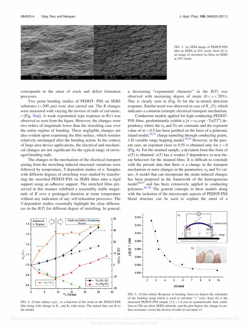
which fails to impede strain localizations.25,28 Figure 3(b)
depicts the cracks observed on Au layers coated on SEBS at
10% strain. It is to be noted that it is possible to strain conven-
tional electrodes (Au) to much higher levels on tailored sub-
strates with additional procedures.30,31 In this context, the
conducting polymer films on SEBS completely differs in the
electrical response in the low strain regime, where the rincreases in (0< x< 15% range). Even for x � 20%, the
strained PEDOT:PSS on SEBS shown in Fig. 3(b) did not
have any evidence of crack or discontinuity formation. These
trends appear as a smooth profile without the presence of a
divergence in R(x) (Fig. 2).
A useful way to portray the stretch induced phenomena
in low dimensional electrical systems is in terms of the mac-
roscopic anisotropy; [r||(x)/r\(x)]. r|| is the film conductivity
in the direction of strain and r\ is the conductivity in the
direction perpendicular to strain and in the plane of the film.
As depicted in (Fig. 4), the anisotropy increases with strain
in the low strain regime (0< x< 10%) where dR||(x)/dx< 0,
indicative of alignment processes and a regime where r||(x)
and r\(x) have competing trends. Beyond �10%, a plateau
in r||(x)/r\(x) is observed as shown in Fig. 4 that basically
corresponds to the regime where similar trends in the r||(x)
and r\(x) response are observed. The initial plateau regime
FIG. 2. (Color online) Conductivity changes on straining: The plot of per-
centage change in surface resistance with strain in the direction of stretch for
a representative five sets of samples. Inset (a) is a schematic of the uni-axial
stretching setup and the self aligning Au-magnet electrodes. Inset (b) shows
the response of film surface resistivity to strain in the direction perpendicular
to the strain.
084525-3 Vijay, Rao, and Narayan J. Appl. Phys. 109, 084525 (2011)
[This article is copyrighted as indicated in the article. Reuse of AIP content is subject to the terms at: http://scitation.aip.org/termsconditions. Downloaded to ] IP:
203.200.35.19 On: Wed, 29 Apr 2015 11:15:35
corresponds to the onset of crack and defect formation
processes.
Two point bending studies of PEDOT: PSS on SEBS
substrates (�200 lm) were also carried out. The R changes
were measured with varying the inverse of radii of curvature,
r [Fig. 5(a)]. A weak exponential type response in R(r) was
observed as seen from the figure. However, the changes were
two orders of magnitude lower than the stretching case over
the entire regime of bending. These negligible changes are
also evident upon examining the film surface, which remains
relatively unchanged after the bending action. In the context
of large area device applications, the electrical and mechani-
cal changes are not significant for the typical range of envis-
aged bending radii.
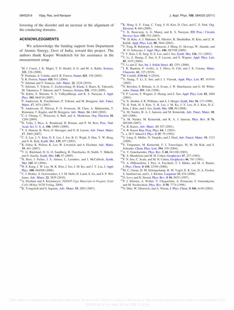
The changes in the mechanism of the electrical transport
arising from the stretching induced structural variations were
followed by temperature, T-dependent studies of r. Samples
with different degrees of stretching were studied by transfer-
ring the stretched PEDOT:PSS on SEBS films onto a rigid
support using an adhesive support. The stretched films pre-
served in this manner exhibited a reasonably stable magni-
tude of R over a prolonged duration at room temperature
without any indication of any self-relaxation processes. The
T-dependent studies essentially highlight the clear differen-
ces in the R(T) for different degree of stretching. In general,
a decreasing “exponential character” in the R(T) was
observed with increasing degree of strain (0< x< 20%).
This is clearly seen in (Fig. 6) for the in-stretch direction
response. Similar trend was observed in case of R\(T), which
indicates a common isotropic electrical transport mechanism.
Conduction models applied for high conducting PEDOT:
PSS films, predominantly exhibit a [r¼r0 exp(�To/T)m] de-
pendency where the r0 and To are constants and the exponent
value of m¼ 0.5 has been justified on the basis of a polaronic
island model,32,33 charge tunneling through conducting grains,
1-D variable range hopping model.34,35 However, in the pres-
ent case, an exponent close to 0.55 is obtained only for x¼ 0
(Fig. 6). For the strained sample, a deviation from this form of
r(T) is obtained. r(T) has a weaker T dependence (a near-lin-
ear behavior) for the strained films. It is difficult to conclude
with the present data that there is a change in the transport
mechanism or mere changes in the parameters; r0 and To val-
ues. A model that can incorporate the strain induced changes
has been proposed in the framework of the heterogeneous
model36,37 and has been extensively applied to conducting
polymers.36–38 The general concepts in these models along
with the inclusion of the microscopic aspects of PEDOT:PSS
blend structure can be used to explain the onset of a
FIG. 3. (a) SEM image of PEDOT:PSS
film on SEBS at 20% strain. Inset (b) is
an image of stretched Au films on SEBS
at 10% strain.
FIG. 4. (Color online) r||/r\ as a function of the strain in the PEDOT:PSS
film along with change in R\ and R|| with strain. The dotted lines are fit to
the model.
FIG. 5. (Color online) Response to bending: Inset (a) depicts the schematic
of the bending setup which is used to calculate “r” (cm). Inset (b) is the
measured PEDOT:PSS sample (3.2� 1.8 cm) in symmetrically bent condi-
tion on 200 lm thick SEBS substrate, and the plot depicts the change in sur-
face resistance versus the inverse of radii of curvature (r).
084525-4 Vijay, Rao, and Narayan J. Appl. Phys. 109, 084525 (2011)
[This article is copyrighted as indicated in the article. Reuse of AIP content is subject to the terms at: http://scitation.aip.org/termsconditions. Downloaded to ] IP:
203.200.35.19 On: Wed, 29 Apr 2015 11:15:35
semimetallic type response r(T). However, extensive investi-
gation is required to comprehensively understand the changes
induced by straining.
The bulk and the surface morphology of PEDOT:PSS
has been studied extensively.34,35,39,40 Conducting hydropho-
bic PEDOT globules are thought to be surrounded by longer
hydrophilic PSS chains in an aqueous dispersion, which
upon spin coating and secondary doping form randomly ori-
ented micrometer sized domains containing aligned PEDOT
rich granules (�25 nm).34 The correlations between mechan-
ical stress and electrical conductivity of conducting polymers
from aqueous suspensions coated on elastomeric substrates
are expected to be complex. However, the effect of straining
PEDOT:PSS films can be understood in terms of the orienta-
tion and extension of the granular regions of PEDOT that are
embedded in the PSS matrix. For doing this, we consider an
effective medium model of differential effective medium
approximation (DEMA). In the DEMA model that originated
from the Bruggermann equation, the Maxwell Garnett gener-
alizations and Cohen et al.’s work, one calculates the effec-
tive physical coefficients of a multiphase system through
multiple scattering approximations of various fields such as
the electric field.41–43 Each grain (of a different phase, vary-
ing in shape, size, and di-electric constant e) is incrementally
introduced to the matrix, and the scattering contribution
from the newly added grain is integrated at every step. The
resultant is then used as a background matrix in the next
step, for the next added grain. The effective medium model
has been used successfully to explain the observed optical
and transport features of conducting polymers and other
organic devices.44–47 However, in our case, a differential
form of the model was necessitated to model the dynamical
changes in morphology that are expected upon straining.
The system under consideration in our case consists of
spherical conducting grains in an insulating matrix similar to
the morphology exhibited by PEDOT:PSS. A similar model
system where DEMA has been applied successfully is in the
studies of polyelectrolyte systems by Oliver et al.,48 where
enhancement of transport properties in the strain direction
and decrease in the transport coefficients in the normal direc-
tion are interpreted in terms of a two phase DEMA model.
The two phase model by Oliver et al. is modeled as a granu-
lar conducting phase, associated with oriented molecular
structures, which dynamically change from spherical
domains to prolate domains upon straining, and are sur-
rounded by an insulating phase at all times. Upon the model-
ing of these topological effects, the system then exhibits an
increased conductivity in the direction of strain along with a
strain induced anisotropy, which is understood by the
decreased scattering of the field in the r|| direction and an
increased scattering in the r\ direction. This is similar to
what we observed in PEDOT:PSS up to strain levels of
<15%, where an enhancement of r|| and a decrease in r\measurements are observed with increasing strain. The r||(x)
and r\(x) trends obtained are similar to the extrapolated
dependencies at low strain regimes of the model. In our sim-
plified EMA model, the sample is modeled by considering
rectangular conductive unit cells separated by insulating
boundaries in place of a globular model. Upon straining
(along the x direction), the dimensions of these cells change
from dx, dy, and dz to kdx, Hkdy, and Hkdz; where k is the
strain ratio. The area of the face of a unit cell varies as (k)�1
in the strain direction and as Hk normal to the strain. Consid-
ering the unit cell boundary area as the rate determining step
for r and enforcing volume conservation conditions with
strain, the function r(k) is determined to be r|| ! k2 and r\! 1/Hk. These dependencies are plotted in terms of the
strain (x) and resistance (R) in Fig. 4 as dotted lines. A good
match with the experimental data for both r||(x) and r\(x) is
observed in the lower strain regimes (<15%).
However at higher strain regimes (>15%), which can be
taken as a limit strain for application of this model for the
PEDOT:PSS on SEBS, defect nucleation, distribution and
propagation start dominating, and a departure from the trends
predicted from the model are observed in the defect dominat-
ing regime (Fig. 4). At these strain levels, the morphological
variations are expected to be severe where defect dynamics
need to be modeled along with DEMA to arrive at a com-
plete picture at all strain regimes.
IV. CONCLUSION
In summary, the strain dependent electrical transport in
PEDOT:PSS thin films reveal interesting features. We empha-
size the importance of substrates and propose SEBS as a
potential candidate for flexible organic electronics applica-
tions. A novel method to monitor r in situ during the straining
process was devised to implement the studies. Pristine
PEDOT:PSS film stretched to large strains (28%) maintained
its film integrity. A minima in the response of R(x) with uni-
axial strain prior to a monotonic increment was observed.
This response, which indicated a decrease � of 15% in
R magnitude and the strain induced anisotropy in r, was
modeled in the framework of the DEMA model. R(T) exhib-
ited a general trend of an effective decrease in temperature de-
pendence as a function of strain (<20%), suggesting a
FIG. 6. (Color online) Temperature dependence: Surface resistance as a
function of T for PEDOT:PSS films with different degrees of strain. Ln(r) vs
(1000/T0.5) for 0, 10, and 20% strained samples are shown in the insets (a),
(b), and (c), respectively.
084525-5 Vijay, Rao, and Narayan J. Appl. Phys. 109, 084525 (2011)
[This article is copyrighted as indicated in the article. Reuse of AIP content is subject to the terms at: http://scitation.aip.org/termsconditions. Downloaded to ] IP:
203.200.35.19 On: Wed, 29 Apr 2015 11:15:35
lowering of the disorder and an increase in the alignment of
the conducting domains.
ACKNOWLEDGMENTS
We acknowledge the funding support from Department
of Atomic Energy, Govt of India, toward this project. The
authors thank Kasper Wenderich for his assistance in the
measurement setup.
1M. J. Currie, J. K. Mapel, T. D. Heidel, S. G. and M. A. Baldo, Science.
321, 226 (2008).2P. Peumans, S. Uchida, and S. R. Forrest, Nature 425, 158 (2003).3S. R. Forrest, Nature 428, 911 (2004).4T. Sekitani and T. Someya, Adv. Mater. 22, 2228 (2010).5T. Sekitani, T. Yokota, U. Zschieschang, H. Klauk, S. Bauer, K. Takeuchi,
M. Takamiya, T. Sakurai, and T. Someya, Science 326, 1516 (2009).6D. Kabra, S. Shriram, N. S. Vidhyadhiraja, and K. S. Narayan, J. Appl.
Phys. 101, 064510 (2007).7P. Andersson, R. Forchheimer, P. Tehrani, and M. Berggren, Adv. Funct.
Mater. 17, 3074 (2007).8P. Andersson, D. Nilsson, P. O. Svensson, M. Chen, A. Malmstrom, T.
Remonen, T. Kugler, and M. Berggren, Adv. Mater. 14, 1460 (2002).9C.-J. Chiang, C. Winscom, S. Bull, and A. Monkman, Org. Electron 10,
1268 (2009).10D. Vella, J. Bico, A. Boudaoud, B. Roman, and P. M. Reis, Proc. Natl.
Acad. Sci. U. S. A. 106, 10901 (2009).11T. S. Hansen, K. West, O. Hassager, and N. B. Larsen, Adv. Funct. Mater.
17, 3069 (2007).12C. S. Lee, J. Y. Kim, D. E. Lee, J. Joo, B. G. Wagh, S. Han, Y. W. Beag,
and S. K. Koh, Synth. Met. 139, 457 (2003).13K. Fehse, K. Walzer, K. Leo, W. Lovenich, and A. Elschner, Adv. Mater.
19, 441 (2007).14T. G. Backlund, H. G. O. Sandberg, R. Osterbacka, H. Stubb, T. Makela,
and S. Jussila, Synth. Met. 148, 87 (2005).15H. Rost, J. Ficker, J. S. Alonso, L. Leenders, and I. McCulloch, Synth.
Met. 145, 83 (2004).16H. S. Kang, J. W. Lee, M. K. Kim, J. Joo, J. M. Ko, and J. Y. Lee, J. Appl.
Phys. 100, 064508 (2006).17C. J. Brabec, S. Gowrisanker, J. J. M. Halls, D. Laird, S. Jia, and S. P. Wil-
liams, Adv. Mater. 22, 3839 (2010).18A. Elschner and S. Kirchmeyer, PEDOT-Type Materials in Organic Solar
Cells (Wiley-VCH Verlag, 2009).19K. Tvingstedt and O. Inganas, Adv. Mater. 19, 2893 (2007).
20K. Hong, S. Y. Yang, C. Yang, S. H. Kim, D. Choi, and C. E. Park, Org.
Electron. 9, 864 (2008).21V. K. Basavaraj, A. G. Manoj, and K. S. Narayan, IEE Proc.: Circuits
Devices Syst. 150, 552 (2003).22W. H. Kim, A. J. Makinen, N. Nikolov, R. Shashidhar, H. Kim, and Z. H.
Kafafi, Appl. Phys. Lett. 80, 3844 (2002).23T. Tong, B. Babatope, S. Admassie, J. Meng, O. Akwogu, W. Akande, and
W. O. Soboyejo, J. Appl. Phys. 106, 083708 (2009).24J. Y. Kim, J. H. Jung, D. E. Lee, and J. Joo, Synth. Met. 126, 311 (2002).25T. Li, Z. Huang, Z. Suo, S. P. Lacour, and S. Wagner, Appl. Phys. Lett.
85, 3435 (2004).26T. Li and Z. Suo, Int. J. Solids Struct. 43, 2351 (2006).27J. R. Bautista, F. Aviles, A. I. Oliva, O. Ceh, and J. E. Corona, Mater.
Character. 61, 325 (2010).28M. Cordill, JOM 62, 9 (2010).29Y. Xiang, T. Li, Z. Suo, and J. J. Vlassak, Appl. Phys. Lett. 87, 161910
(2005).30N. Bowden, S. Brittain, A. G. Evans, J. W. Hutchinson, and G. M. White-
sides, Nature 393, 146 (1998).31S. P. Lacour, S. Wagner, Z. Huang, and Z. Suo, Appl. Phys. Lett. 82, 2404
(2003).32A. N. Aleshin, S. R. Williams, and A. J. Heeger, Synth. Met. 94, 173 (1998).33D. H. Park, H. S. Kim, Y. B. Lee, J. M. Ko, J.-Y. Lee, H.-J. Kim, D.-C.
Kim, J. Kim, and J. Joo, Synth. Met. 158, 90 (2008).34A. M. Nardes, R. A. J. Janssen, and M. Kemerink, Adv. Funct. Mater. 18,
865 (2008).35A. M. Nardes, M. Kemerink, and R. A. J. Janssen, Phys. Rev. B 76,
085208 (2007).36A. B. Kaiser, Adv. Mater. 13, 927 (2001).37A. B. Kaiser Rep. Prog. Phys. 64, 1 (2001).38e. a. M T Ahmed J. Phys. D 25, 79 (1992).39U. Lang, E. Muller, N. Naujoks, and J. Dual, Adv. Functi. Mater. 19, 1215
(2009).40S. Timpanaro, M. Kemerink, F. J. Touwslager, M. M. De Kok, and S.
Schrader, Chem. Phys. Lett. 394, 339 (2004).41A. V. Goncharenko, Phys. Rev. E 68, 041108 (2003).42K. S. Mendelson and M. H. Cohen, Geophysics 47, 257 (1982).43P. N. Sen, C. Scala, and M. H. Cohen, Geophysics 46, 781 (1981).44S. A. DiBenedetto, I. Paci, A. Facchetti, T. J. Marks, and M. A. Ratner,
J. Phys. Chem. B 110, 22394 (2006).45M. C. Gurau, D. M. Delongchamp, B. M. Vogel, E. K. Lin, D. A. Fischer,
S. Sambasivan, and L. J. Richter, Langmuir 23, 834 (2006).46O. Levy and D. Stroud, Phys. Rev. B 56, 8035 (1997).47P. J. Seoome, A. Wolter, Y. Cheguettine, A. Pronacute, F. Genoudcoise,
and M. Nechtschein, Phys. Rev. B 58, 7774 (1998).48O. Durr, W. Dieterich, and A. Nitzan, J. Phys. Chem. B 106, 6149 (2002).
084525-6 Vijay, Rao, and Narayan J. Appl. Phys. 109, 084525 (2011)
[This article is copyrighted as indicated in the article. Reuse of AIP content is subject to the terms at: http://scitation.aip.org/termsconditions. Downloaded to ] IP:
203.200.35.19 On: Wed, 29 Apr 2015 11:15:35