
towards conducting and photolumin - RSC Publishing
12
Multifunctional behavior of molecules comprising stacked cytosine–Ag I –cytosine base pairs; towards conducting and photoluminescence silver-DNA nanowires† F ´ atima Linares, * a Emilio Garc ´ ıa-Fern ´ andez, b F. Javier L ´ opez-Garz ´ on, c Mar ´ ıa Domingo-Garc ´ ıa, c Angel Orte, b Antonio Rodr ´ ıguez-Di ´ eguez c and Miguel A. Galindo * c DNA molecules containing a 1D silver array may be applied for nanotechnology applications, but first their conducting and photoluminescence behavior must be enhanced. Here we have synthesized and characterized three new helical compounds based on stacked silver–mediated cytosine base pairs [Ag(mC) 2 ]X (mC ¼ N1-methylcytosine; X ¼ NO 3 (1), BF 4 (2) and ClO 4 (3)), that contain uninterrupted polymeric Ag I chains that run through the center of the helixes, comparable to related silver-DNA structures. The exposure of nanostructures of [Ag(mC) 2 ]BF 4 (2) to cold hydrogen plasma stimulates the reduction of the prearranged Ag I polymeric chains to metallic silver along the material. This solvent-free reduction strategy leads to the compound [Ag I (mC) 2 ]X@Ag 0 (2H) that contains uniformly well-distributed silver metallic nanostructures that are responsible for the new conducting and photoluminescence properties of the material. The presence of silver nanostructures alongside compound 2H has been evaluated by means of X-ray photoelectron spectroscopy (XPS), UV-vis spectroscopy, and X-ray powder diffraction (XRPD). The conducting and photoactive properties of 2H were studied by electrostatic force microscopy (EFM) and conducting-AFM (c-AFM), and photoluminescence microscopy (PL), respectively. The results demonstrate that the presence of well-organized metallic silver nanoentities on the material is responsible for the novel conductivity and photoactive properties of the material. This methodology can be employed for the generation of multifunctional silver-DNA related materials with tailored properties. Introduction Nanotechnology applications rely on the capability to prepare and control functional materials at the nanoscale with high precision. 1–3 The development of novel methodologies that enhance this control has attracted the attention of scientists worldwide. In particular, the development of new strategies towards the fabrication of nanowires with tailored electronic and optical properties has been the subject of extensive efforts due to the practical applications they may offer for the miniaturization of electronic circuits. Importantly, in order to design new nanocircuits the correct organization of the nanowires must be precisely controlled. In this context, DNA has become an important tool for scientists, since intricate functional nano- structures can be prepared based on its sequence programma- bility, which offers potential applications in nanomachinery, sensing devices, drug delivery, and information processing. 4–6 However, the concept of exploiting the self-organizing properties of DNA to create nanocircuits remains a great challenge and the source of much contentious discussion. 7,8 This is due to the debatable conducting properties in natural DNA molecules, with some reports pointing towards the insulating behavior of long DNA molecules, 9,10 whilst other studies have demonstrated charge transfer in short DNA molecules. 11,12 The electronic properties of DNA molecules have been enhanced using various strategies, including the covalent attachment of functional groups 13,14 or the deposition of a conducting material, 15 a Unidad de Microscop´ ıa de Fuerza At´ omica, Centro de Instrumentaci´ on Cient´ ıca, Universidad de Granada, Paseo Prof. Juan Osorio s/n, 18003, Granada, Spain. E-mail: [email protected] b Departamento de Fisicoqu´ ımica, Facultad de Farmacia, Universidad de Granada, Campus Cartuja, 18071, Granada, Spain c Departamento de Qu´ ımica Inorg´ anica, Facultad de Ciencias, Universidad de Granada, Avd. Fuentenueva s/n, 18071, Granada, Spain. E-mail: [email protected] † Electronic supplementary information (ESI) available: Extended information on this article is available for bond distances ( ˚ A) (molecular structures of 1–3); XPS survey spectra, FITR spectroscopy; valence band XPS and UV-vis spectra for 2 and 2H; additional photoemission images; EFM measurement, phase shi vs. bias voltages and EFM and c-AFM measurements for 2, before reduction with cold hydrogen plasma; optical microscope image showing crystals of 2H employed during c-AFM studies. CCDC 1847831–1847833. For ESI and crystallographic data in CIF or other electronic format see DOI: 10.1039/c8sc04036b Cite this: Chem. Sci. , 2019, 10, 1126 All publication charges for this article have been paid for by the Royal Society of Chemistry Received 11th September 2018 Accepted 4th November 2018 DOI: 10.1039/c8sc04036b rsc.li/chemical-science 1126 | Chem. Sci., 2019, 10, 1126–1137 This journal is © The Royal Society of Chemistry 2019 Chemical Science EDGE ARTICLE Open Access Article. Published on 08 noviembre 2018. Downloaded on 29/12/2021 4:09:24 a.m.. This article is licensed under a Creative Commons Attribution-NonCommercial 3.0 Unported Licence. View Article Online View Journal | View Issue
-
Upload
khangminh22 -
Category
Documents
-
view
4 -
download
0
Transcript of towards conducting and photolumin - RSC Publishing

ChemicalScience
EDGE ARTICLE
Ope
n A
cces
s A
rtic
le. P
ublis
hed
on 0
8 no
viem
bre
2018
. Dow
nloa
ded
on 2
9/12
/202
1 4:
09:2
4 a.
m..
Thi
s ar
ticle
is li
cens
ed u
nder
a C
reat
ive
Com
mon
s A
ttrib
utio
n-N
onC
omm
erci
al 3
.0 U
npor
ted
Lic
ence
.
View Article OnlineView Journal | View Issue
Multifunctional b
aUnidad de Microscopıa de Fuerza Atomica
Universidad de Granada, Paseo Prof. Jua
E-mail: [email protected] de Fisicoquımica, Facultad
Campus Cartuja, 18071, Granada, SpaincDepartamento de Quımica Inorganica, Facul
Avd. Fuentenueva s/n, 18071, Granada, Spa
† Electronic supplementary information (Ethis article is available for bond distancessurvey spectra, FITR spectroscopy; valenand 2H; additional photoemission imagbias voltages and EFM and c-AFM meascold hydrogen plasma; optical microsemployed during c-AFM studies. CCDcrystallographic data in CIF or o10.1039/c8sc04036b
Cite this: Chem. Sci., 2019, 10, 1126
All publication charges for this articlehave been paid for by the Royal Societyof Chemistry
Received 11th September 2018Accepted 4th November 2018
DOI: 10.1039/c8sc04036b
rsc.li/chemical-science
1126 | Chem. Sci., 2019, 10, 1126–1137
ehavior of molecules comprisingstacked cytosine–AgI–cytosine base pairs; towardsconducting and photoluminescence silver-DNAnanowires†
Fatima Linares, *a Emilio Garcıa-Fernandez, b F. Javier Lopez-Garzon, c
Marıa Domingo-Garcıa,c Angel Orte, b Antonio Rodrıguez-Dieguez c
and Miguel A. Galindo *c
DNA molecules containing a 1D silver array may be applied for nanotechnology applications, but first their
conducting and photoluminescence behavior must be enhanced. Here we have synthesized and
characterized three new helical compounds based on stacked silver–mediated cytosine base pairs
[Ag(mC)2]X (mC ¼ N1-methylcytosine; X ¼ NO3 (1), BF4 (2) and ClO4 (3)), that contain uninterrupted
polymeric AgI chains that run through the center of the helixes, comparable to related silver-DNA
structures. The exposure of nanostructures of [Ag(mC)2]BF4 (2) to cold hydrogen plasma stimulates the
reduction of the prearranged AgI polymeric chains to metallic silver along the material. This solvent-free
reduction strategy leads to the compound [AgI(mC)2]X@Ag0 (2H) that contains uniformly well-distributed
silver metallic nanostructures that are responsible for the new conducting and photoluminescence
properties of the material. The presence of silver nanostructures alongside compound 2H has been
evaluated by means of X-ray photoelectron spectroscopy (XPS), UV-vis spectroscopy, and X-ray powder
diffraction (XRPD). The conducting and photoactive properties of 2H were studied by electrostatic force
microscopy (EFM) and conducting-AFM (c-AFM), and photoluminescence microscopy (PL), respectively.
The results demonstrate that the presence of well-organized metallic silver nanoentities on the material
is responsible for the novel conductivity and photoactive properties of the material. This methodology
can be employed for the generation of multifunctional silver-DNA relatedmaterials with tailored properties.
Introduction
Nanotechnology applications rely on the capability to prepareand control functional materials at the nanoscale with highprecision.1–3 The development of novel methodologies thatenhance this control has attracted the attention of scientists
, Centro de Instrumentacion Cientıca,n Osorio s/n, 18003, Granada, Spain.
de Farmacia, Universidad de Granada,
tad de Ciencias, Universidad de Granada,
in. E-mail: [email protected]
SI) available: Extended information on(A) (molecular structures of 1–3); XPS
ce band XPS and UV-vis spectra for 2es; EFM measurement, phase shi vs.
urements for 2, before reduction withcope image showing crystals of 2HC 1847831–1847833. For ESI andther electronic format see DOI:
worldwide. In particular, the development of new strategiestowards the fabrication of nanowires with tailored electronic andoptical properties has been the subject of extensive efforts due tothe practical applications they may offer for the miniaturizationof electronic circuits. Importantly, in order to design newnanocircuits the correct organization of the nanowires must beprecisely controlled. In this context, DNA has become animportant tool for scientists, since intricate functional nano-structures can be prepared based on its sequence programma-bility, which offers potential applications in nanomachinery,sensing devices, drug delivery, and information processing.4–6
However, the concept of exploiting the self-organizing propertiesof DNA to create nanocircuits remains a great challenge and thesource of much contentious discussion.7,8 This is due to thedebatable conducting properties in natural DNAmolecules, withsome reports pointing towards the insulating behavior of longDNA molecules,9,10 whilst other studies have demonstratedcharge transfer in short DNA molecules.11,12 The electronicproperties of DNA molecules have been enhanced using variousstrategies, including the covalent attachment of functionalgroups13,14 or the deposition of a conducting material,15
This journal is © The Royal Society of Chemistry 2019

Edge Article Chemical Science
Ope
n A
cces
s A
rtic
le. P
ublis
hed
on 0
8 no
viem
bre
2018
. Dow
nloa
ded
on 2
9/12
/202
1 4:
09:2
4 a.
m..
Thi
s ar
ticle
is li
cens
ed u
nder
a C
reat
ive
Com
mon
s A
ttrib
utio
n-N
onC
omm
erci
al 3
.0 U
npor
ted
Lic
ence
.View Article Online
including different metal atoms (i.e. Ag, Pd, Cu, Au, and Rh).Metallization of DNA molecules has proved to afford DNA-nanowires with improved conductivity,7,16–20 and has commonlybeen achieved through binding of metal ions to a DNA templatefollowed by reduction of the ions positioned along the structure,typically using chemical, photochemical or electrochemicalreduction.21 However, this strategy cannot guarantee thecomplete control over the deposition process, and variousregions can be metalized to different extents, hampering theability of metal–DNA-based systems to conduct electricity. A newway to precisely control the stoichiometry and the position of themetal ions have been proven using DNA molecules containingthe so-called metal-mediated base pairs. In these cases, themetal ions are placed inside the double helix structure, byprogramming its sequence, with hydrogen bonding that holdsthe two stands together being replaced by coordination bondsbetween the bases. Following this strategy continuous 1D linearchains of AgI ions can be generated inside the DNA duplex,22
thus demonstrating that new metallo-DNA nanowires could berationally prepared. Studies of the conducting properties ofthese types of systems remain ongoing and no clear conclusionsregarding the enhancement of their conductivity have beendrawn yet. DNA molecules containing C–AgI–C silver-mediatedbase pairs (C ¼ cystosine) have been well studied,22–24 and inthe last decade several conducting studies have been performedon such metallized DNAmolecules. The results indicate that theincrease or decrease of charge transfer may depend on the DNAsequence employed.25,26 A recent study shows that the interca-lation of AgI ions between the mismatched cytosine bases leadsto more efficient charge transfer.27 However, a potential methodto increase the conductivity of these systems would be to reduceof the conned AgI ions to Ag0. It is well known that the reduc-tion of controlled amounts of silver ions introduced on DNAstrands leads to the formation and stabilization of silver nano-clusters (AgNCs) which have photoluminescence properties dueto their small size (<2 nm).28,29 In these instances, the reductionof AgI–DNA complexes is carried out in solution,30–32 andconsequently the native structure of the resulting AgNC–DNAsystems can be signicantly altered.33 If high-precision nano-circuit architectures based on DNA molecules containing silver-mediated base pairs, with conductive and/or photoemissiveproperties, are to be developed, a methodology that leads to theformation of metallic silver whilst preserving the structure of thematerial will be needed. In this regard, methodologies based onphotoreduction processes can promote the reduction of thesilver ions to metallic silver along DNA molecules;34 however thepresence of solvents with additional chemical functionalities (i.e.salts35 and hydroxyl groups36) has been proven to play animportant role in the reduction process. Our attempts to usea solvent- and additive-free photoreduction methodology,exclusively using UV irradiation over 1 to 12 h (254 nm), wereunsuccessful to form well-distributed silver metallic throughoutthe herein studied 1D nanostructures. A new approach to beexplored is the use of controlled cold hydrogen plasma topromote the reduction of silver ions to afford metallic silverwhilst maintaining the integrity of previously organized Ag-material nanostructures in the solid state. In principle, this
This journal is © The Royal Society of Chemistry 2019
strategy could be used to reduce silver ions organized in DNAmolecules comprising silver-mediated base pairs once they havebeen correctly organized and immobilized on a surface support.Moreover, such an approach will avoid the use of any additionalsolvents and/or chemicals, which can disrupt the organization ofthe structures. Finally, this proposed strategy could enable theformation of uniformly distributed nanoscale metallic silverentities along the solid material, which ultimately may improvethe conducting and/or photoemissive properties of the material.
With the aim of proving this hypothesis, in this work weexplore the use of cold hydrogen plasma to reduce silver ionsconned in helixes consisting of contiguous C–AgI–C base pairs,in order to promote the formation of well-organized metallicsilver, which may subsequently enhance the conducting andphotoactive properties of the nanomaterial. We have chosen thesehelical complexes as an initial approach towards the study ofmorecomplex DNA double helix structures since the stabilizing effect ofcytosine towards the formation of AgNC is well known. Themolecular structure of the herein described silver complexes,studied by X-ray diffraction, conrmed the formation of doublehelixes containing an uninterrupted 1D silver chain that runsthrough the central axis. These complexes can be formed ona solid surface support and their morphology and conductingproperties were studied by atomic force microcopy (AFM), electricforce microscopy (EFM) and conducting AFM (c-AFM). Wedemonstrate by means of X-ray photoelectron spectroscopy (XPS),solid UV-vis spectroscopy, X-ray powder diffraction (XRPD) andphotoluminescence (PL) microscopy that the silver ions can bereduced by exposure to cold hydrogen plasma, leading to theformation of silver nanostructures that are uniformly distributedalong the structures. Finally, we prove that the presence of thesemetallic silver nanospecies can enhance both the conductivity andphotoluminescence behavior of the material, as indicated by EFMand c-AFM analysis, and PL microscopy, respectively.
Results and discussionSynthesis and characterization of the complexes
The formation of helixes 1, 2 and 3 was carried out by reactionof methylcytosine (mC) with the corresponding AgI salt; nitrate,tetrauoroborate or perchlorate, respectively. In all cases, singlecrystals of complexes [Ag(mC)2]X (X ¼ NO3, BF4, ClO4), suitablefor X-ray diffraction analysis, were obtained within the next 48 hupon slow evaporation of the reaction solution. In all cases, theanalysis of the molecular structure, by means of X-ray diffrac-tion, revealed the formation of helixes consisting of stackedmC–AgI–mC homobase pairs. The silver-mediated base pairsare lined up on top of each other giving rise to the formation ofargentophilic interactions that run through the centre of thehelix. Inter-cytosine-pair hydrogen bonds are also observedwhich further support the formation of the helical structures.These assemblies resemble the structure recently reported byTerron et al. for the formation of a double helix generated bycontiguous hC–AgI–hC base pairs (hC ¼ hexylcytosine).37 Animportant difference of the herein reported structures is theobtaining of individual chiral crystals for 2 and 3, although theoverall samples were racemic mixtures. In addition, the three
Chem. Sci., 2019, 10, 1126–1137 | 1127

Chemical Science Edge Article
Ope
n A
cces
s A
rtic
le. P
ublis
hed
on 0
8 no
viem
bre
2018
. Dow
nloa
ded
on 2
9/12
/202
1 4:
09:2
4 a.
m..
Thi
s ar
ticle
is li
cens
ed u
nder
a C
reat
ive
Com
mon
s A
ttrib
utio
n-N
onC
omm
erci
al 3
.0 U
npor
ted
Lic
ence
.View Article Online
polymeric silver chains show shorter argentophilic contacts,probably due to the presence of less steric effects induced by themethyl group compared to the hexyl alkyl chains.
Compound 1 crystallizes in the monoclinic space group P21/c.The asymmetric unit consists of ten [Ag(mC)2]
+ units, ten nitrateanions and ten crystallization water molecules (Fig. 1a). The AgI
ions are two-coordinated and adopt a linear geometry. The mCunits act as monodentate ligands and coordinate to the silverions via their N1 atom [Ag–N1 2.102(15) to 2.250(20) A] formingsilver-mediated base pairs, mC–AgI–mC. The base pairs areorganized on top of each other leading to the formation ofargentophilic interactions [Ag–Ag 2.902(2) to 3.088(2) A], whichare signicantly shorter than those found in an analogous silverdouble helix [3.162 to 3.235 A]37 and in a DNA molecule with an1D array of silver ions [3.2 to 3.4 A].22 ThemC units are in a cisoidorientation showing propeller twist angles from 48.79 to 66.32�.This Watson–Crick pairing arrangement is different to the anti-Watson–Crick (transoid) orientation described inside a DNAduplex38 and in a particular silver complex where two AgI ions
Fig. 1 (a) Scheme for the [Ag(mC)2]+ silver-mediated base pair. (b)
Different perspectives of the polymeric [Ag(mC)2]NO3 in the asym-metric unit of 1 and (c) in the asymmetric unit of [Ag(mC)2]BF4 (2).Counter ions and crystallization water molecules have been omittedfor clarity. (d) View of 2 from the crystallographic b axis (Ag, yellowsphere; mC ligand, grey; BF4, blue).
1128 | Chem. Sci., 2019, 10, 1126–1137
coordinate via N–Ag–O connectivity in mC ligands.39 In addition,DFT calculations indicate that the transoid orientation in C–AgI–C pairs may be favoured.40 However, the occurrence of the cisoidarrangement is not exceptional, and it has been also described inthe structure reported by Terron et al.37 as well as inside DNA22
and RNA23 molecules.In complex 1, as well as in 2 and 3 (vide infra), the cisoid
arrangement is preferred, which is stabilized by the formationof contiguous p–p interactions [distance between the centroidspertaining to mC rings from 3.477 to 4.199 A] as well ashydrogen bonds between the keto and amino groups of diag-onal opposite mC ligands of the two complementary strands[hydrogen bonds in the range of 2.843 to 3.022 A].
All these interactions give rise to the formation of a doublehelix structure consisting of consecutive mC–AgI–mC base pairsthat include an uninterrupted 1D silver array running throughthe helical axis. Interestingly, the silver array is not completelylinear all along the asymmetric unit and different <Ag–Ag–Agangles [137.69� to 179.22�] can be observed (Fig. 1b). A completeturn of the helix contains an average of ten base pairs within theasymmetric unit. The helix diameter is c.a. 11 A.
In the case of compounds 2 and 3, the selected crystals aresimilar right-handed helix compounds, and therefore only thedata for 2 are described here. Complex 2 crystallizes in themonoclinic space group P212121. The asymmetric unit consists ofeight [Ag(mC)2]
+ units and eight crystallization tetrauoroborateanions (Fig. 1c). In the same way as 1, the AgI ions coordinate totwo mC units via their N1 atom [Ag–N1 range 2.149(12)–2.206(10)A] adopting a linear geometry and generating chains formed bysilver-mediated base pairs mC–AgI–mC. The argentophilic inter-actions [Ag–Ag 2.9025(16) to 2.9786(16)A] are also shorter thanthose previously found for an analogous system,37 and relatedsilver-DNA molecule.22 The mC units are in a cisoid orientationshowing propeller twist angles [32.53� to 68.74�]. This arrange-ment facilitates the formation of contiguous p–p interactions[distance between the centroids from 3.550 to 3.929 A] that areinterrupted every six silver-mediated base pairs. The presence ofhydrogen bonds is also observed between the keto and aminogroups of diagonal oppositemC ligands of the two complementarystrands. All these interactions support the formation of a doublehelix structure analogous to 1. In this case the linearity of the silverarray is slightly more disrupted than that in compound 1 (<Ag–Ag–Ag angles from [125.44� to 169.85�]) (Fig. 1c). The helix turn is nowcompleted every nine base pairs and consequently comprises twoasymmetric units. The helix diameter is also c.a. 11 A.
Surface studies of complexes [Ag(mC)2]X [X ¼ NO3 (1), BF4, (2)ClO4 (3)]
Atomic force microscopy (AFM) was employed to study themorphology of the silver chains of complexes 1, 2 and 3immobilized on solid substrate surfaces. The synthesis of thecomplexes was carried out both on mica and silicon substratesby drop-casting of a solution containing mC and AgI ions(details in the Experimental section) and waiting until allsolvent evaporates. Initial efforts to form 1, 2 or 3 on surfacesshowed that the complex organization depends on both the
This journal is © The Royal Society of Chemistry 2019
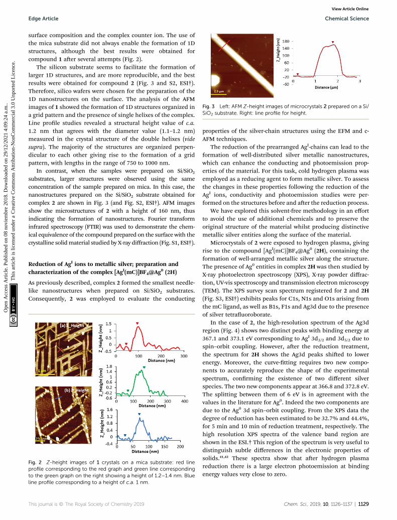
Fig. 3 Left: AFM Z-height images of microcrystals 2 prepared on a Si/SiO2 substrate. Right: line profile for height.
Edge Article Chemical Science
Ope
n A
cces
s A
rtic
le. P
ublis
hed
on 0
8 no
viem
bre
2018
. Dow
nloa
ded
on 2
9/12
/202
1 4:
09:2
4 a.
m..
Thi
s ar
ticle
is li
cens
ed u
nder
a C
reat
ive
Com
mon
s A
ttrib
utio
n-N
onC
omm
erci
al 3
.0 U
npor
ted
Lic
ence
.View Article Online
surface composition and the complex counter ion. The use ofthe mica substrate did not always enable the formation of 1Dstructures, although the best results were obtained forcompound 1 aer several attempts (Fig. 2).
The silicon substrate seems to facilitate the formation oflarger 1D structures, and are more reproducible, and the bestresults were obtained for compound 2 (Fig. 3 and S2, ESI†).Therefore, silico wafers were chosen for the preparation of the1D nanostructures on the surface. The analysis of the AFMimages of 1 showed the formation of 1D structures organized ina grid pattern and the presence of single helixes of the complex.Line prole studies revealed a structural height value of c.a.1.2 nm that agrees with the diameter value (1.1–1.2 nm)measured in the crystal structure of the double helixes (videsupra). The majority of the structures are organized perpen-dicular to each other giving rise to the formation of a gridpattern, with lengths in the range of 750 to 1000 nm.
In contrast, when the samples were prepared on Si/SiO2
substrates, larger structures were observed using the sameconcentration of the sample prepared on mica. In this case, thenanostructures prepared on the Si/SiO2 substrate obtained forcomplex 2 are shown in Fig. 3 (and Fig. S2, ESI†). AFM imagesshow the microstructures of 2 with a height of 160 nm, thusindicating the formation of nanostructures. Fourier transforminfrared spectroscopy (FTIR) was used to demonstrate the chem-ical equivalence of the compound prepared on the surface with thecrystalline solidmaterial studied by X-ray diffraction (Fig. S1, ESI†).
Reduction of AgI ions to metallic silver; preparation andcharacterization of the complex [AgI(mC)]BF4@Ag0 (2H)
As previously described, complex 2 formed the smallest needle-like nanostructures when prepared on Si/SiO2 substrates.Consequently, 2 was employed to evaluate the conducting
Fig. 2 Z-height images of 1 crystals on a mica substrate: red lineprofile corresponding to the red graph and green line correspondingto the green graph on the right showing a height of 1.2–1.4 nm. Blueline profile corresponding to a height of c.a. 1 nm.
This journal is © The Royal Society of Chemistry 2019
properties of the silver-chain structures using the EFM and c-AFM techniques.
The reduction of the prearranged AgI-chains can lead to theformation of well-distributed silver metallic nanostructures,which can enhance the conducting and photoemission prop-erties of the material. For this task, cold hydrogen plasma wasemployed as a reducing agent to form metallic silver. To assessthe changes in these properties following the reduction of theAgI ions, conductivity and photoemission studies were per-formed on the structures before and aer the reduction process.
We have explored this solvent-free methodology in an effortto avoid the use of additional chemicals and to preserve theoriginal structure of the material whilst producing distinctivemetallic silver entities along the surface of the material.
Microcrystals of 2 were exposed to hydrogen plasma, givingrise to the compound [AgI(mC)]BF4@Ag0 (2H), containing theformation of well-arranged metallic silver along the structure.The presence of Ag0 entities in complex 2H was then studied byX-ray photoelectron spectroscopy (XPS), X-ray powder diffrac-tion, UV-vis spectroscopy and transmission electronmicroscopy(TEM). The XPS survey scan spectrum registered for 2 and 2H(Fig. S3, ESI†) exhibits peaks for C1s, N1s and O1s arising fromthe mC ligand, as well as B1s, F1s and Ag3d due to the presenceof silver tetrauoroborate.
In the case of 2, the high-resolution spectrum of the Ag3dregion (Fig. 4) shows two distinct peaks with binding energy at367.1 and 373.1 eV corresponding to AgI 3d3/2 and 3d5/2 due tospin–orbit coupling. However, aer the reduction treatment,the spectrum for 2H shows the Ag3d peaks shied to lowerenergy. Moreover, the curve-tting requires two new compo-nents to accurately reproduce the shape of the experimentalspectrum, conrming the existence of two different silverspecies. The two new components appear at 366.8 and 372.8 eV.The splitting between them of 6 eV is in agreement with thevalues in the literature for Ag0. Indeed the two components aredue to the Ag0 3d spin–orbit coupling. From the XPS data thedegree of reduction has been estimated to be 32.7% and 44.4%,for 5 min and 10 min of reduction treatment, respectively. Thehigh resolution XPS spectra of the valence band region areshown in the ESI.† This region of the spectrum is very useful todistinguish subtle differences in the electronic properties ofsolids.41,42 These spectra show that aer hydrogen plasmareduction there is a large electron photoemission at bindingenergy values very close to zero.
Chem. Sci., 2019, 10, 1126–1137 | 1129
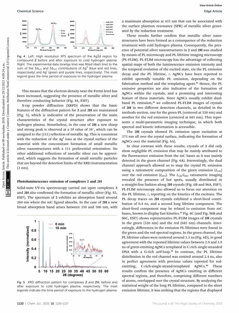
Fig. 4 Left: High resolution XPS spectrum of the Ag3d region forcompound 2 before and after exposure to cold hydrogen plasma.Right: The experimental data (orange line) was fitted (dash line) to thesum of the 3d5/2 and 3d3/2 contributions of Ag0 (blue and red lines,respectively) and AgI (green and purple lines, respectively). The insetlegend gives the time period of exposure to the hydrogen plasma.
Chemical Science Edge Article
Ope
n A
cces
s A
rtic
le. P
ublis
hed
on 0
8 no
viem
bre
2018
. Dow
nloa
ded
on 2
9/12
/202
1 4:
09:2
4 a.
m..
Thi
s ar
ticle
is li
cens
ed u
nder
a C
reat
ive
Com
mon
s A
ttrib
utio
n-N
onC
omm
erci
al 3
.0 U
npor
ted
Lic
ence
.View Article Online
This means that the electron density near the Fermi level hasbeen increased, suggesting the presence of metallic silver andtherefore conducting behavior (Fig. S4, ESI†).
X-ray powder diffraction (XRPD) shows that the basicfeatures of the diffraction pattern for 2 and 2H are maintained(Fig. 5), which is indicative of the preservation of the maincharacteristics of the crystal structure aer exposure tohydrogen plasma. Nonetheless, in the case of 2H a new sharpand strong peak is observed at a 2q value of 38�, which can beassigned to the (111) reection of metallic Ag. This is consistentwith the reduction of the AgI ions at the crystal surface of thematerial with the concomitant formation of small metallicsilver nanostructures with a 111 preferential orientation. Noother additional reections of metallic silver can be appreci-ated, which suggests the formation of small metallic particlesthat are beyond the detection limits of the XRD instrumentation(3 nm).
Photoluminescence emission of complexes 2 and 2H
Solid-state UV-vis spectroscopy carried out upon complexes 2and 2H also conrmed the formation of metallic silver (Fig. S5,ESI†). The spectrum of 2 exhibits an absorption band around260 nm where the mC ligand absorbs. In the case of 2H a newbroad absorption band arises between 350 and 500 nm, with
Fig. 5 XRD diffraction pattern for complexes 2 and 2H, before andafter exposure to cold hydrogen plasma, respectively. The insetlegends indicate the time period of exposure to the hydrogen plasma.
1130 | Chem. Sci., 2019, 10, 1126–1137
a maximum absorption at 435 nm that can be associated withthe surface plasmon resonance (SPR) of metallic silver gener-ated by the reduction treatment.
These results further conrm that metallic silver nano-structures have been formed as a consequence of the reductiontreatment with cold hydrogen plasma. Consequently, the pres-ence of potential silver nanostructures in 2 and 2H was studiedby means of PL microscopy and PL lifetime imaging microscopy(PL-FLIM). PL-FLIM microscopy has the advantage of collectingspatial maps of both the luminescence emission intensity andthe temporal evolution of the excited state, via the PL emissiondecay and the PL lifetime, s. AgNCs have been reported toexhibit spectrally tunable PL emission, depending on thefabrication method and the templating agent.43 Hence, the PLemissive properties are also indicative of the formation ofAgNCs within the crystals, and a promising and interestingfeature of these materials. Since AgNCs usually exhibit dual-band PL emission,44 we collected PL-FLIM images of crystalsof 2H in two different detection channels, as detailed in themethods section, one for the green PL (centered at 520 nm) andanother for the red emission (centered at 685 nm). This repre-sents a multi-parametric imaging technique, in which bothspectral and kinetic information is accessible.
The 2H crystals showed PL emission upon excitation at375 nm all over the crystal surface, indicating the formation ofAgNCs over the material (Fig. 6A).
In clear contrast with these results, crystals of 2 did onlyshow negligible PL emission that may be mainly attributed tothe uorescence emission from the mC bases as it was mainlydetected in the green channel (Fig. 6A). Interestingly, the dualchannel approach allowed us to map the crystal PL emissionusing a ratiometric composition of the green emission (I520)over the red emission (I685). The I520/I685 ratiometric imagingrevealed the presence of hot spots, usually distributed ina straight-line fashion along 2H crystals (Fig. 6B and S6A, ESI†).PL-FLIM microscopy also allowed us to focus our attention onthe PL lifetime, s, reporting on the kinetics of the excitons. ThePL decay traces on 2H crystals exhibited a short-lived contri-bution of 0.4 ns, and a second long lifetime component. Theshort-lived component may be related to emission from mCbases, known to display fast kinetics.45 Fig. 6C (and Fig. S6B andS6C, ESI†) shows representative PL-FLIM images of 2H crystalsin the green (520 nm) and the red (685 nm) channels. Inter-estingly, differences in the emission PL lifetimes were found inthe green and the red spectral regions. In the green channel, thePL lifetime values were centered around 3.3 ns (Fig. 6D), in goodagreement with the reported lifetime values between 2.9 and 3.9ns of green-emitting AgNCs templated in C-rich single-strandedDNA with a G-rich self-loop.38 In contrast, the PL lifetimedistribution in the red channel was centred around 2.4 ns, alsoin perfect agreement with previous values reported for red-emitting, C-rich-single-strand-templated AgNCs.46 Theseresults conrm the presence of AgNCs emitting in differentspectral regions, and therefore, comprising different numbersof atoms, overlapped over the crystal structure. By analyzing thestatistical weight of the long PL lifetime, compared to the shortemission lifetime, it was striking that the regions that displayed
This journal is © The Royal Society of Chemistry 2019
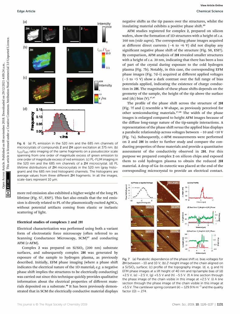
Fig. 6 (a) PL emission in the 520 nm and the 685 nm channels ofmicrocrystals of compounds 2 and 2H upon excitation at 375 nm. (b)I520/I685 ratio imaging of the same fragments on a pseudocolor scalespanning from one order of magnitude excess of green emission toone order of magnitude excess of red emission. (c) PL-FLIM imaging inthe 520 nm and the 685 nm channels of a 2H microcrystal. (d) PLlifetime distributions of 2H microcrystals in the 520 nm (gray histo-gram) and the 685 nm (red histogram) channels. The histograms areaverage values from three different 2H fragments. In all the images,scale-bars represent 10 mm.
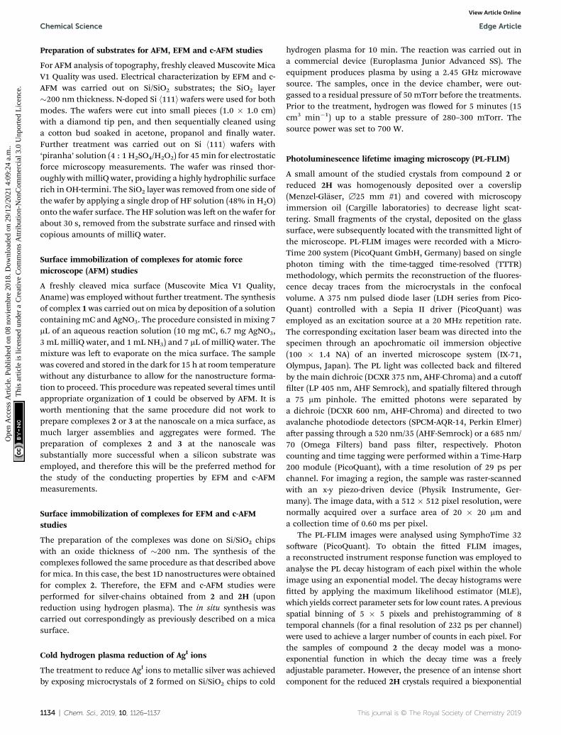
Fig. 7 (a) Parabolic dependence of the phase shift vs. bias voltages for2H between �10 and 10 V; (b) Z-height image of the chain aligned ona Si/SiO2 surface; (c) profile of the topography image. (d, e, g and h)EFM phase images at a lift height of 40 nm and tip/sample bias of (d)+2.5 V, (e) �2.5 V, (g) +5.5 V and (h) �5.5 V. (f) A line section throughthe phase image of the chain visible in this image at +2.5 V. (i) A linesection through the phase image of the chain visible in this image at+5.5 V. The cantilever spring constant (k)¼ 129.9 Nm�1 and the qualityfactor (Q) ¼ 274.
Edge Article Chemical Science
Ope
n A
cces
s A
rtic
le. P
ublis
hed
on 0
8 no
viem
bre
2018
. Dow
nloa
ded
on 2
9/12
/202
1 4:
09:2
4 a.
m..
Thi
s ar
ticle
is li
cens
ed u
nder
a C
reat
ive
Com
mon
s A
ttrib
utio
n-N
onC
omm
erci
al 3
.0 U
npor
ted
Lic
ence
.View Article Online
more red emission also exhibited a higher weight of the long PLlifetime (Fig. S7, ESI†). This fact also entails that the red emis-sion is directly related to PL of the plasmonically excited AgNCs,without potential artifacts coming from elastic or inelasticscattering of light.
Electrical studies of complexes 2 and 2H
Electrical characterization was performed using both a variantform of electrostatic force microscopy (oen referred to asScanning Conductance Microscopy, SCM)47 and conductingAFM (c-AFM).
Complex 2 was prepared on Si/SiO2 (200 nm) substratesurfaces, and subsequently complex 2H was generated byexposure of the sample to hydrogen plasma, as previouslydescribed. Initially, EFM phase imaging (where a phase shiindicates the electrical nature of the 1D material; e.g. a negativephase shi implies the structures to be electrically conducting)was carried out since this technique quickly provides qualitativeinformation about the electrical properties of different mate-rials deposited on a substrate.48 It has been previously demon-strated that in SCM the electrically conductive material displays
This journal is © The Royal Society of Chemistry 2019
negative shis as the tip passes over the structures, whilst theinsulating material exhibits a positive phase shi.49
AFM studies registered for complex 2, prepared on siliconwafers, show the formation of 1D structures with a height of c.a.160 nm (vide supra). The corresponding phase images acquiredat different direct currents (�6 to +6 V) did not display anysignicant negative phase shi of the structure (Fig. S8, ESI†).By comparison, AFM analysis of 2H revealed smaller structureswith a height of c.a. 30 nm, indicating that there has been a lossof part of the crystal during exposure to the cold hydrogenplasma (Fig. 7b). Notably, in this case, the corresponding EFMphase images (Fig. 7d–i) acquired at different applied voltages(�5 to +5 V) show a dark contrast over the full range of biaspotentials applied, indicating the existence of charge conduc-tion in 2H. The magnitude of these phase shis depends on thegeometry of the sample, the height of the tip above the surfaceand (dc) bias (V).17,47
The prole of the phase shi across the structure of 2H(Fig. 7f and i) resemble a W-shape, as previously perceived forother semiconducting materials.17,20 The width of the phaseimages is enlarged compared to height AFM images because ofthe diffuse long-range nature of the tip-sample interactions. Arepresentation of the phase shi versus the applied bias displaysa parabolic relationship across voltages between �10 and +10 V(Fig. 7a). Subsequently, c-AFM measurements were performedon 2 and 2H in order to further study and compare the con-ducting properties of these materials and provide a quantitativeassessment of the conductivity observed in 2H. For thispurpose we prepared complex 2 on silicon chips and exposedthem to cold hydrogen plasma to obtain the reduced 2Hmaterial. A drop of Ga–In eutectic was placed at the end of thecorresponding microcrystal to provide an electrical contact.
Chem. Sci., 2019, 10, 1126–1137 | 1131

Fig. 8 PinPoint c-AFM height image of the 2H chain. (a) Z-heightimage (height 400 nm); (b) current signal at +10 V. (c) Dual Line profilefrom the Z-height image (red line) and current map (green line),highlighting that the current associated with this structure is of theorder of nanoamps. (d) F–d curve for PinPoint c-AFM mode. Selectedparameters: control height: 1.8 mm; stiffness threshold: 1.20 nN;approach time: 4.0ms; retract time: 2.0ms; (e) 3D overlay for Z-heightand current signals (X : Y : Z ¼ 1 : 1 : 1.5).
Chemical Science Edge Article
Ope
n A
cces
s A
rtic
le. P
ublis
hed
on 0
8 no
viem
bre
2018
. Dow
nloa
ded
on 2
9/12
/202
1 4:
09:2
4 a.
m..
Thi
s ar
ticle
is li
cens
ed u
nder
a C
reat
ive
Com
mon
s A
ttrib
utio
n-N
onC
omm
erci
al 3
.0 U
npor
ted
Lic
ence
.View Article Online
The metallic AFM tip was then used to act as the secondelectrical contact to the sample. During our initial c-AFMexperiments we found that the high forces exerted upon thesamples by the tip result in individual chains being brokenduring the raster scanning of the tip across the sample (resultsnot shown). In order to avoid this problem, larger structures of2 and 2H were employed for c-AFM studies, compared to thoseemployed for EFM measurements, since they were less proneto damage during scanning, though still required carefulregulation of the applied force by the tip using PinPointTM(Park Systems) c-AFM Mode. Moreover the exposure time tohydrogen plasma was also reduced to 7 minutes as longerexposure times appeared to weaken the structures for thesesets of experiments.
The initial c-AFM experiments performed on 2 demonstratedthe absence of perceptible conducting properties, in agreementwith the results obtained by EFM. The area of the samplesurface scanned during measurements was located c.a. 50 mmaway from the eutectic contact on a 100 mm long crystal (Fig. S9,ESI†). In this regard, while we have not observed conductivityfor 2, it is worth noting that previous studies performed onpolycytosine sequences of 11 mer C–AgI–C base pairs, by meansof scanning tunneling microscopy break-junction, revealedhigher single molecule conductance with respect to thecanonical G–C oligonucleotide, although the technique and thesample are different to that reported here.27
In contrast, when the measurements were performed for 2Hthe results showed a notable increase in conductance, whichagrees with the EFM results. Fig. 8 illustrates the topography ofa structure of 2H and its electrical properties when a voltage of�10 V is applied to the sample, demonstrating the presence ofa current signal throughout 2H. The average heights of thestructures were c.a. 400 nm indicating that they consist ofmultiple silver-chains bundled together into thickerassemblies.
In this case, the area of the sample surface scanned duringmeasurements was located at 85 mm away from the eutecticcontact on the crystal chosen for the measurements (Fig. S10,ESI†). A current map simultaneously acquired alongside theheight data is shown in Fig. 8b, at an applied bias of +10 V andon the order of up to 1 nA. The zero current observed when thetip was placed above a clean area of the Si/SiO2 substrate provesthat the measured current is a consequence of the electricalproperties of 2H.
Fig. 8b also shows the existence of different conductingregions, which may be explained by poor mechanical contactbetween the tip and an uneven surface with depressions (Fig. 8e).
The maximum specic conductivity registered for thisstructure was 1.25 nA and demonstrated that the use of coldhydrogen plasma can promote the formation of metallic silvernanostructures in 2H that ultimately enhance the conductingproperties of the material. It is worth mentioning that inessence, the size of the material, the amount of metal coatingand the distance to the Ga–In eutectic electrode inuence theconducting properties of the sample. In this regard, DNA-basedsilver molecules, which can resemble the herein reported
1132 | Chem. Sci., 2019, 10, 1126–1137
structures, have shown different conductivity depending of theconditions of the experiments.
However, in these previous studies different amounts ofsilver ions were initially deposited along DNA templates andthen reduced to form metallic silver using diverse procedures(e.g. chemical reduction or electrochemical process). In general,the resulting structures displayed metallic silver granularaggregates along the DNA molecules and signicant conduc-tivity (50 to 400 nA)16,50,51 compared to the herein reportedmaterial, when a bias/potential was applied. Recently, narrowand smooth DNA-silver nanowires were obtained by trans-ferring silver atoms from silver nanoparticles (AgNPs) to DNAmolecules, although no conducting data were reported.52
However, following a similar procedure using gold nano-particles (AuNPs), small (less than 13 nm height), narrow anduniform DNA-gold structures were obtained which showeda long range conductivity of c.a. 1 nA.7
Importantly, the herein reported strategy does not alter theinitial composition of the material, does not require the use ofadditional chemicals to promote the reduction of the AgI ions,and is able to enhance the conductivity and photoemissionbehavior of the pre-organized material. The reduction of AgI
within the material may generate thin lms of silver nano-structures along the material that are in sufficient intimatecontact (via metal/metal contact interactions) to allow chargemigration through the material. Therefore, this methodologycan be employed to enhance the conducting properties of
This journal is © The Royal Society of Chemistry 2019

Edge Article Chemical Science
Ope
n A
cces
s A
rtic
le. P
ublis
hed
on 0
8 no
viem
bre
2018
. Dow
nloa
ded
on 2
9/12
/202
1 4:
09:2
4 a.
m..
Thi
s ar
ticle
is li
cens
ed u
nder
a C
reat
ive
Com
mon
s A
ttrib
utio
n-N
onC
omm
erci
al 3
.0 U
npor
ted
Lic
ence
.View Article Online
various solid materials containing well organized AgI in thesolid state without the addition of other chemicals.
Conclusions
Three different helical silver complexes 1, 2 and 3 have beenprepared and characterized by single crystal X-ray diffraction.The molecular structure revealed the formation of helixes con-sisting of stacked mC–AgI–mC homobase pairs, with the pres-ence of contiguous AgI chains running through the centre of thehelixes and with the presence of argentophilic interactions, thatresemble DNA molecules containing a 1D array of silver ions.22
The complexes were also prepared on solid support surfacesand their morphology, conductivity and photoluminescencebehavior were studied by means of AFM, EFM, c-AFM, and PLmicroscopy, respectively. In an effort to enhance the conductingand photoemissive properties of these materials, complex 2 wasexposed to cold hydrogen plasma, leading to the formation ofcompound 2H possessing metallic silver nanostructures alongthe material. The presence of metallic silver was conrmed byXPS, UV-vis spectroscopy, XPRD and PL-FLIM. XPRD alsoconrmed that the reduction process did not alter the crystalstructure of the complex. Compound 2H showed PL emissionalong the structure that reveals the formation of plasmonicemissive silver nanoclusters. In consequence, the presence ofthese metallic silver nanoentities signicantly improved thephotoemissive properties of the material. Moreover, the con-ducting properties of 2H were evaluated by EFM and c-AFM,conrming the new conducting behavior of the material,which can be also attributed to the presence of metallic silverentities. Although more studies will be required to compre-hensively evaluate how electrical charges travel through thismaterial, it is reasonable to propose that the observedconductivity is dominated by a conduction bridge through thewell-ordered metallic entities. Importantly, these results offera new strategy to prepare and modify the conducting and pho-toluminescence properties of a solid material that containsprearranged silver ion chains, e.g. DNA molecules containingsequential silver-mediated base pairs, even at the nanoscale.
ExperimentalMaterials
Reagents were purchased from Aldrich and used as received.N1-methylcytosine was synthesized according to literaturemethods.53 Elemental analysis was performed on a ThermoScientic Flash 2000, and UV-vis spectra were recorded on anAgilent Technologies Cary 100 Spectrophotometer. XPS spectrawere recorded on a Kratos Axis Ultra DLD spectrometer.Monochromatic AlKa radiation in constant analyser energymode with a pass energy of 160 and 20 eV (for the survey andhigh resolution spectra, respectively) was used. The C 1s tran-sition at 285 eV was used as the reference value. Aer back-ground correction, the high-resolution spectra were tted toLorentzian and Gaussian curves using XPS CASA soware. In allcases, a standard Shirley baseline was used to separate the realsignal from the background.54 A JASCO 6200 FTIR
This journal is © The Royal Society of Chemistry 2019
Spectrophotometer with SPECTRA MANAGER v2 soware wasused to obtain infrared spectra in the mid-infrared area (4000–400 cm�1) with a resolution of 0.25 cm�1.
General procedure for the synthesis of [Ag(N1-methylcytosine)2]X (X ¼ NO3 (1), BF4 (2), ClO4 (3))
A general procedure will proceed as follows; to a water solutionof N1-methylcytosine (mC) (150 mg, 1.2 mmol) was addeda water solution of the corresponding silver salt (0.6 mmol). Thesolution was stirred for 30 min in the dark and then ltered offthrough a syringe lter (0.45 mm cellulose acetate membrane) toremove any insoluble impurities. The clear solution was le tocrystallize and aer a few days crystals suitable for X-raydiffraction were collected. In the case of complex 1, a non-crystalline phase was also obtained as a white powder.
[Ag(N1-methylcytosine)2]NO3 (1): Yield 21%. ElementalAnalysis corresponding to [C10H14N7O5Ag$(H2O)1.4]: calcd C26.96, N 22.01, H 3.80; found, C 26.63, N 22.23, H 3.79. [Ag(N1-methylcytosine)2]BF4 (2): Yield 35%. Elemental Analysis corre-sponding to [C10H14N6O2BF4Ag$(H2O)0.5]: calcd C 26.45, N18.51, H 3.33; found, C 26.49, N 18.13, H 3.66. [Ag(N1-methylcytosine)2]ClO4 (3): Yield 33%. Elemental Analysis cor-responding to [C10H14N6O6ClAg$(H2O)0.5]: calcd C 25.74, N18.01, H 3.24; found, C 25.89, N 18.14, H 3.52.
Single-crystal X-ray structure determination
X-ray data collection of suitable single crystals of compounds 1–3 was done at 100(2) K on a Bruker VENTURE area detectorequipped with graphite monochromated Mo-Ka radiation (l ¼0.71073 A) by applying the u-scan method. The data reductionwas performed with APEX2 soware55 and corrected forabsorption using SADABS.56 Crystal structures were solved bydirect methods using the SIR97 program57 and rened by full-matrix least-squares on F2 including all reections usinganisotropic displacement parameters by means of the Olex2v1.2 crystallographic package58 and the SHELXL-2014program.59,60 All hydrogen atoms were included as xedcontributions riding on attached atoms with isotropic thermaldisplacement parameters 1.2 times or 1.5 times those of theirparent atoms for the organic ligands. In general, the overallquality of the crystals was low and this results in a low diffrac-tion for the three compounds. Several crystals of 1, 2 and 3 weremeasured and the structure was solved from the best data wewere able to collect. Attempts to solve disorder problems withtwo nitrate and ten crystallization water molecules with twotetrauoroborate anions and with one perchlorate anion failedin compounds 1, 2 and 3, respectively. We have used theBYPASS procedure61 implemented in Olex2 v1.2 to eliminatethese molecules. Final R(F), wR(F2) and goodness of t agree-ment factors, details on the data collection and analysis can befound in Table S1 (ESI).†
Details of the bond distances of compounds are summarizedin Table S2 (ESI).† Crystallographic data (excluding structurefactors) for the structures reported in this paper have beendeposited with the Cambridge Crystallographic Data Center assupplementary publication no. CCDC 1847831–1847833.
Chem. Sci., 2019, 10, 1126–1137 | 1133
Chemical Science Edge Article
Ope
n A
cces
s A
rtic
le. P
ublis
hed
on 0
8 no
viem
bre
2018
. Dow
nloa
ded
on 2
9/12
/202
1 4:
09:2
4 a.
m..
Thi
s ar
ticle
is li
cens
ed u
nder
a C
reat
ive
Com
mon
s A
ttrib
utio
n-N
onC
omm
erci
al 3
.0 U
npor
ted
Lic
ence
.View Article Online
Preparation of substrates for AFM, EFM and c-AFM studies
For AFM analysis of topography, freshly cleaved Muscovite MicaV1 Quality was used. Electrical characterization by EFM and c-AFM was carried out on Si/SiO2 substrates; the SiO2 layer�200 nm thickness. N-doped Si h111i wafers were used for bothmodes. The wafers were cut into small pieces (1.0 � 1.0 cm)with a diamond tip pen, and then sequentially cleaned usinga cotton bud soaked in acetone, propanol and nally water.Further treatment was carried out on Si h111i wafers with‘piranha’ solution (4 : 1 H2SO4/H2O2) for 45min for electrostaticforce microscopy measurements. The wafer was rinsed thor-oughly with milliQ water, providing a highly hydrophilic surfacerich in OH-termini. The SiO2 layer was removed from one side ofthe wafer by applying a single drop of HF solution (48% in H2O)onto the wafer surface. The HF solution was le on the wafer forabout 30 s, removed from the substrate surface and rinsed withcopious amounts of milliQ water.
Surface immobilization of complexes for atomic forcemicroscope (AFM) studies
A freshly cleaved mica surface (Muscovite Mica V1 Quality,Aname) was employed without further treatment. The synthesisof complex 1 was carried out onmica by deposition of a solutioncontainingmC and AgNO3. The procedure consisted inmixing 7mL of an aqueous reaction solution (10 mg mC, 6.7 mg AgNO3,3 mLmilliQ water, and 1 mL NH3) and 7 mL of milliQ water. Themixture was le to evaporate on the mica surface. The samplewas covered and stored in the dark for 15 h at room temperaturewithout any disturbance to allow for the nanostructure forma-tion to proceed. This procedure was repeated several times untilappropriate organization of 1 could be observed by AFM. It isworth mentioning that the same procedure did not work toprepare complexes 2 or 3 at the nanoscale on a mica surface, asmuch larger assemblies and aggregates were formed. Thepreparation of complexes 2 and 3 at the nanoscale wassubstantially more successful when a silicon substrate wasemployed, and therefore this will be the preferred method forthe study of the conducting properties by EFM and c-AFMmeasurements.
Surface immobilization of complexes for EFM and c-AFMstudies
The preparation of the complexes was done on Si/SiO2 chipswith an oxide thickness of �200 nm. The synthesis of thecomplexes followed the same procedure as that described abovefor mica. In this case, the best 1D nanostructures were obtainedfor complex 2. Therefore, the EFM and c-AFM studies wereperformed for silver-chains obtained from 2 and 2H (uponreduction using hydrogen plasma). The in situ synthesis wascarried out correspondingly as previously described on a micasurface.
Cold hydrogen plasma reduction of AgI ions
The treatment to reduce AgI ions to metallic silver was achievedby exposing microcrystals of 2 formed on Si/SiO2 chips to cold
1134 | Chem. Sci., 2019, 10, 1126–1137
hydrogen plasma for 10 min. The reaction was carried out ina commercial device (Europlasma Junior Advanced SS). Theequipment produces plasma by using a 2.45 GHz microwavesource. The samples, once in the device chamber, were out-gassed to a residual pressure of 50 mTorr before the treatments.Prior to the treatment, hydrogen was owed for 5 minutes (15cm3 min�1) up to a stable pressure of 280–300 mTorr. Thesource power was set to 700 W.
Photoluminescence lifetime imaging microscopy (PL-FLIM)
A small amount of the studied crystals from compound 2 orreduced 2H was homogenously deposited over a coverslip(Menzel-Glaser, B25 mm #1) and covered with microscopyimmersion oil (Cargille laboratories) to decrease light scat-tering. Small fragments of the crystal, deposited on the glasssurface, were subsequently located with the transmitted light ofthe microscope. PL-FLIM images were recorded with a Micro-Time 200 system (PicoQuant GmbH, Germany) based on singlephoton timing with the time-tagged time-resolved (TTTR)methodology, which permits the reconstruction of the uores-cence decay traces from the microcrystals in the confocalvolume. A 375 nm pulsed diode laser (LDH series from Pico-Quant) controlled with a Sepia II driver (PicoQuant) wasemployed as an excitation source at a 20 MHz repetition rate.The corresponding excitation laser beam was directed into thespecimen through an apochromatic oil immersion objective(100 � 1.4 NA) of an inverted microscope system (IX-71,Olympus, Japan). The PL light was collected back and lteredby the main dichroic (DCXR 375 nm, AHF-Chroma) and a cutofflter (LP 405 nm, AHF Semrock), and spatially ltered througha 75 mm pinhole. The emitted photons were separated bya dichroic (DCXR 600 nm, AHF-Chroma) and directed to twoavalanche photodiode detectors (SPCM-AQR-14, Perkin Elmer)aer passing through a 520 nm/35 (AHF-Semrock) or a 685 nm/70 (Omega Filters) band pass lter, respectively. Photoncounting and time tagging were performed within a Time-Harp200 module (PicoQuant), with a time resolution of 29 ps perchannel. For imaging a region, the sample was raster-scannedwith an x-y piezo-driven device (Physik Instrumente, Ger-many). The image data, with a 512 � 512 pixel resolution, werenormally acquired over a surface area of 20 � 20 mm anda collection time of 0.60 ms per pixel.
The PL-FLIM images were analysed using SymphoTime 32soware (PicoQuant). To obtain the tted FLIM images,a reconstructed instrument response function was employed toanalyse the PL decay histogram of each pixel within the wholeimage using an exponential model. The decay histograms weretted by applying the maximum likelihood estimator (MLE),which yields correct parameter sets for low count rates. A previousspatial binning of 5 � 5 pixels and prehistogramming of 8temporal channels (for a nal resolution of 232 ps per channel)were used to achieve a larger number of counts in each pixel. Forthe samples of compound 2 the decay model was a mono-exponential function in which the decay time was a freelyadjustable parameter. However, the presence of an intense shortcomponent for the reduced 2H crystals required a biexponential
This journal is © The Royal Society of Chemistry 2019

Edge Article Chemical Science
Ope
n A
cces
s A
rtic
le. P
ublis
hed
on 0
8 no
viem
bre
2018
. Dow
nloa
ded
on 2
9/12
/202
1 4:
09:2
4 a.
m..
Thi
s ar
ticle
is li
cens
ed u
nder
a C
reat
ive
Com
mon
s A
ttrib
utio
n-N
onC
omm
erci
al 3
.0 U
npor
ted
Lic
ence
.View Article Online
model in which one of the decay timeswas xed at 0.4 ns, whereasthe other decay time was a freely adjustable parameter. To high-light the distribution of times, amplitude intensity images of eachdecay time were reported in combination with a lifetime image.
I520/I685 ratio images were obtained by dividing the intensityimages collected in each channel, and the ratio represented bya pseudo-color scale, with the image intensity modulated by thetotal I520 + I685 intensity, via a home-coded script in MathCad15.0 (PTC).
Scanning probe microscopy (AFM, EFM and c-AFM)
AFM imaging was performed in non-contact mode in air, usingan NX20 Park Systems instrument (Park Systems Corp.), withACTA cantilevers (silicon cantilevers, resonant frequency 200–400 kHz, spring force constant 25–75 N m�1, Park Systems).Data acquisition was carried out using SmartScan sowareversion 1.0 and XEI Data Processing and Analysis sowareversion 4.3.0 Build2 (Park Systems Corp). The NX20 equipmentis supported by an Active Vibration Isolation System (AVIS)model AVI-200S/LP (Table Stable Ltd).
A variant method of EFM has been used as a contactlessmeans of qualitatively assessing the electrical properties of 2structures prior to quantitative measurement of conductivity.The method is based on the storage of energy in the tip/chain/substrate capacitor and the chain conductance inuences themeasurement via the RC time constant for polarization of thenanocrystals. A detailed description of the operation of thismethod has been reported elsewhere.17,62 The phase shibetween the driving force and the tip motion is recorded asa function of applied dc bias (V) as the tip crosses above thechain at a constant li height (typically a value set within therange of 40–100 nm). EFMmeasurements were performed usinga two-pass method, in which the rst pass of the tip over a scanline gathers topographical data in standard non-contact mode,and the second pass of the tip records the EFM phase infor-mation. During the second pass, the tip travelled over thesample surface at a constant li height (set at 40 nm), whilst anindependently controlled dc bias was applied to the sample(from �1.5 to �10 V), with the tip grounded. The cantileversused for these measurements were NCSTAu which are designedfor non-contact or so tapping mode imaging. A metallic layer(Au) is coated on both sides of the cantilever. The typical tipradius of curvature is less than 50 nm. These probes are 140–160mm long, with a resonant frequency of about 129.9 kHz,a quality factor Q ¼ 274, and a spring constant between 1.2 and29 N m�1.
Conductive AFM (c-AFM) was performed at room tempera-ture with the gentle PinPoint i-AFM mode which was the key toacquiring reproducible and reliable topography and c-AFMimages on the 2 chains. The conventional contact andconductive AFM have pros and cons, but this mode allows thebest of both spatial resolution and current sensitivity, whilstminimizing the lateral forces with optimized current measure-ment over different sample surfaces. The measurement proce-dure can be explained in three steps: (1) the XY scanner stopsduring acquisition; (2) the tip approaches the surface, measures
This journal is © The Royal Society of Chemistry 2019
the current and retracts from the surface over a few ms (4 ms) toachieve an interaction force preset (1.2 nN); (3) record theapproach height and maintain the Z distance. The force washeld constant while the current is measured, and then the tip isretracted and moved to the next pixel. This method differssignicantly from conventional c-AFM because the tip retractsand approaches each pixel rather than adjusting the tip heightto maintain a constant oscillation amplitude. This scan modedoes require more time (approximately 30 min for a 256 � 256pixel image) but results in highly reproducible images. Incontrast to conventional c-AFM, this technique eliminates fric-tion, which reduces tip-sample deterioration. For conductivemeasurements (c-AFM), CDTCONTR probes were used (the CDTdiamond coating is highly doped and the total resistancemeasured in contact to a platinum surface is <10 kOhm). Theseprobes are 440–460 mm long, with a resonant frequency of about20 kHz and a spring constant between 0.1 and 1.7 N m�1.Electrical contact was made by applying a drop of In/Ga eutecticto one corner of the chip and to the metallic chuck. The currentis measured directly aer the tip using a preamplier witha gain of 1011 V/A (ULCA). c-AFM imaging was performed withan applied bias of +10 V. The imaged area was about 1 mm awayfrom the In/Ga contact.
Conflicts of interest
There are no conicts to declare.
Acknowledgements
Financial support from the Spanish MINECO (CTQ2017-89311-P), Junta de Andalucıa (FQM-2293) and Universidad de Granada(Reincorporacion Plan Propio) are acknowledged. This studywas partially supported by the “Unidad de Excelencia de Quı-mica aplicada a Biomedicina y Medioambiente”, Universidadde Granada. We thank Dr Scott M. D. Watson for discussionsand guidance during the preparation of the manuscript, and DrIsmael Drubi for technical support.
Notes and references
1 M. R. Jones, N. C. Seeman and C. A. Mirkin, Science, 2015,347, 1260901.
2 P. W. K. Rothemund, Nature, 2006, 440, 297–302.3 N. C. Seeman, Nature, 2003, 421, 427–431.4 O. I. Wilner and I. Willner, Chem. Rev., 2012, 112, 2528–2556.5 Z.-G. Wang, C. Song and B. Ding, Small, 2013, 9, 2210–2222.6 H. Pei, X. Zuo, D. Zhu, Q. Huang and C. Fan, Acc. Chem. Res.,2014, 550, 550–559.
7 A. Stern, G. Eidelshtein, R. Zhuravel, G. I. Livshits, D. Rotem,A. Kotlyar and D. Porath, Adv. Mater., 2018, 1800433.
8 S. M. D. Watson, A. R. Pike, J. Pate, A. Houlton andB. R. Horrocks, Nanoscale, 2014, 6, 4027–4037.
9 A. J. Storm, J. Van Noort, S. De Vries and C. Dekker, Appl.Phys. Lett., 2001, 79, 3881–3883.
Chem. Sci., 2019, 10, 1126–1137 | 1135
Chemical Science Edge Article
Ope
n A
cces
s A
rtic
le. P
ublis
hed
on 0
8 no
viem
bre
2018
. Dow
nloa
ded
on 2
9/12
/202
1 4:
09:2
4 a.
m..
Thi
s ar
ticle
is li
cens
ed u
nder
a C
reat
ive
Com
mon
s A
ttrib
utio
n-N
onC
omm
erci
al 3
.0 U
npor
ted
Lic
ence
.View Article Online
10 P. J. De Pablo, F. Moreno-Herrero, J. Colchero, J. GomezHerrero, P. Herrero, A. M. Baro, P. Ordejon, J. M. Soler andE. Artacho, Phys. Rev. Lett., 2000, 85, 4992–4995.
11 J. D. Slinker, N. B. Muren, S. E. Renfrew and J. K. Barton, Nat.Chem., 2011, 3, 228–233.
12 M. Bixon, B. Giese, S. Wessely, T. Langenbacher,M. E. Michel-Beyerle and J. Jortner, Proc. Natl. Acad. Sci. U.S. A., 1999, 96, 11713–11716.
13 W. Chen and G. B. Schuster, J. Am. Chem. Soc., 2013, 135,4438–4449.
14 T. Nguyen, A. Brewer and E. Stulz, Angew. Chem., Int. Ed.,2009, 48, 1974–1977.
15 K. Ijiro and H. Mitomo, Polym. J., 2017, 49, 815–824.16 E. Braun, Y. Eichen, U. Sivan and G. Ben-Yoseph, Nature,
1998, 391, 775–778.17 R. Hassanien, S. A. F. Al-Said, L. Siller, R. Little, N. G. Wright,
A. Houlton and B. R. Horrocks, Nanotechnology, 2012, 23,075601.
18 H. D. A. Mohamed, S. M. D. Watson, B. R. Horrocks andA. Houlton, J. Mater. Chem. C, 2015, 3, 438–446.
19 A. Houlton, A. R. Pike, M. A. Galindo and B. R. Horrocks,Chem. Commun., 2009, 1797–1806.
20 J. Pate, F. Zamora, S. M. D. Watson, N. G. Wright,B. R. Horrocks and A. Houlton, J. Mater. Chem. C, 2014, 2,9265–9273.
21 Z. Chen, C. Liu, F. Cao, J. Ren and X. Qu, Chem. Soc. Rev.,2018, 47, 4017–4072.
22 J. Kondo, Y. Tada, T. Dairaku, Y. Hattori, H. Saneyoshi,A. Ono and Y. Tanaka, Nat. Chem., 2017, 9, 956–960.
23 J. Kondo, Y. Tada, T. Dairaku, H. Saneyoshi, I. Okamoto,Y. Tanaka and A. Ono, Angew. Chem., Int. Ed., 2015, 54,13323–13326.
24 A. Ono, S. Cao, H. Togashi, M. Tashiro, T. Fujimoto,T. Machinami, S. Oda, Y. Miyake, I. Okamoto andY. Tanaka, Chem. Commun., 2008, 4825–4827.
25 H. Gong and X. Li, Analyst, 2011, 136, 2242–2246.26 Z. Lin, X. Li and H. B. Kraatz, Anal. Chem., 2011, 83, 6896–
6901.27 E. Toomey, J. Xu, S. Vecchioni, L. Rothschild, S. Wind and
G. E. Fernandes, J. Phys. Chem. C, 2016, 120, 7804–7809.28 S. Y. New, S. T. Lee and X. D. Su, Nanoscale, 2016, 8, 17729–
17746.29 E. Gwinn, D. Schultz, S. M. Copp, S. Swasey and S. Ralph,
Nanomaterials, 2015, 5, 180–207.30 J. T. Petty, J. Zheng, N. V. Hud and R. M. Dickson, J. Am.
Chem. Soc., 2004, 126, 5207–5212.31 J. M. Obliosca, C. Liu and H.-C. Yeh, Nanoscale, 2013, 5,
8443–8461.32 I. Dıez and R. H. A. Ras, Nanoscale, 2011, 3, 1963–1970.33 J. T. Petty, O. O. Sergev, M. Ganguly, I. J. Rankine,
D. M. Chevrier and P. Zhang, J. Am. Chem. Soc., 2016, 138,3469–3477.
34 L. Berti, A. Alessandrini and P. Facci, J. Am. Chem. Soc., 2005,127, 11216–11217.
35 A. A. Zinchenko, N. Chen and S. Murata, Chem. Lett., 2008,37, 1096–1097.
1136 | Chem. Sci., 2019, 10, 1126–1137
36 D. Majumdar, A. Singha, P. K. Mondal and S. Kundu, ACSAppl. Mater. Interfaces, 2013, 5, 7798–7807.
37 A. Terron, B. Moreno-Vachiano, A. Bauza, A. Garcıa-Raso,J. J. Fiol, M. Barcelo-Oliver, E. Molins and A. F. Frontera,Chem.–Eur. J., 2017, 23, 2103–2108.
38 H. Liu, F. Shen, P. Haruehanroengra, Q. Yao, Y. Cheng,Y. Chen, C. Yang, J. Zhang, B. Wu, Q. Luo, R. Cui, J. Li,J. Ma, J. Sheng and J. Gan, Angew. Chem., Int. Ed., 2017, 56,9430–9434.
39 T. Kistenmacher, M. Rossi and L. Marzilli, Inorg. Chem.,1979, 18, 240–244.
40 L. A. Espinosa Leal, A. Karpenko, S. Swasey, E. G. Gwinn,V. Rojas-Cervellera, C. Rovira and O. Lopez-Acevedo,J. Phys. Chem. Lett., 2015, 6, 4061–4066.
41 J. Matthew, Surf. Interface Anal., 2004, 36, 1647.42 V. K. Abdelkader-Fernandez, F. Morales-Lara, M. Melguizo,
C. Garcıa-Galların, R. Lopez-Garzon, M. L. Godino-Salido,F. J. Lopez-Garzon, M. Domingo-Garcıa and M. J. Perez-Mendoza, Appl. Surf. Sci., 2015, 357, 1410–1418.
43 Y. Lu and W. Chen, Chem. Soc. Rev., 2012, 41, 3594–3623.44 C. Bu, L. Mu, X. Cao, M. Chen, G. She and W. Shi,
Nanotechnology, 2018, 417, 257–269.45 R. J. Malone, A. M. Miller and B. Kohler, Photochem.
Photobiol., 2003, 77, 158–164.46 C. Li and C. Wei, Sens. Actuators, B, 2017, 240, 451–458.47 M. Al-Hinai, R. Hassanien, S. M. D. Watson, N. G. Wright,
A. Houlton and B. R. Horrocks, Nanotechnology, 2016, 27,095704.
48 C. Staii, A. T. Johnson and N. J. Pinto, Nano Lett., 2004, 4,859–862.
49 M. Bockrath, N. Markovic, A. Shepard, M. Tinkham,L. Gurevich, L. P. Kouwenhoven, M. W. Wu and L. L. Sohn,Nano Lett., 2002, 2, 187–190.
50 S. A. Farha Al-Said, R. Hassanien, J. Hannant, M. A. Galindo,S. Pruneanu, A. R. Pike, A. Houlton and B. R. Horrocks,Electrochem. Commun., 2009, 11, 550–553.
51 G. Ban, R. Dong, K. Li, H. Han and X. Yan, Nanoscale Res.Lett., 2009, 4, 321–326.
52 G. Eidelshtein, N. Fardian-Melamed, V. Gutkin,D. Basmanov, D. Klinov, D. Rotem, Y. Levi-Kalisman,D. Porath and A. Kotlyar, Adv. Mater., 2016, 28, 4839–4844.
53 E. Greco, A. E. Aliev, V. G. H. Latte, K. Bala, D. Duncan,L. Pilon, P. Golding and H. C. Hailes, New J. Chem., 2010,34, 2634–2642.
54 V. K. Abdelkader, M. Domingo-Garcıa, M. Melguizo,R. Lopez-Garzon, F. Javier Lopez-Garzon and M. Perez-Mendoza, Carbon, 2015, 93, 276–285.
55 Bruker, APEX3 Soware, Bruker AXS Inc., Madison,Wisconsin, USA, vol. 1, 2016.
56 G. M. Sheldrick, Program for Empirical Adsorption Correction,Inst. Inorg. Chem. Univ. Gottingen, Ger., 1996.
57 A. Altomare, M. C. Burla, M. Camalli, G. L. Cascarano,C. Giacovazzo, A. Guagliardi, A. Grazia, G. Moliterni,G. Polidori and R. Spagna, J. Appl. Crystallogr., 1999, 32,115–119.
58 L. J. Farrugia, J. Appl. Crystallogr., 2012, 45, 849–854.
This journal is © The Royal Society of Chemistry 2019

Edge Article Chemical Science
Ope
n A
cces
s A
rtic
le. P
ublis
hed
on 0
8 no
viem
bre
2018
. Dow
nloa
ded
on 2
9/12
/202
1 4:
09:2
4 a.
m..
Thi
s ar
ticle
is li
cens
ed u
nder
a C
reat
ive
Com
mon
s A
ttrib
utio
n-N
onC
omm
erci
al 3
.0 U
npor
ted
Lic
ence
.View Article Online
59 G. M. Sheldrick, Program for Crystal Structure Renement,Univ. Gottingen, Ger., 2014.
60 G. M. Sheldrick, Acta Crystallogr., Sect. A: Found. Crystallogr.,2008, 64, 112–122.
This journal is © The Royal Society of Chemistry 2019
61 A. L. Spek and IUCr, Acta Crystallogr., Sect. C: Struct. Chem.,2015, 71, 9–18.
62 A. Houlton and S. M. D. Watson, Annu. Rep. Prog. Chem., Sect.A: Inorg. Chem., 2011, 107, 21–42.
Chem. Sci., 2019, 10, 1126–1137 | 1137