Chemical Science - RSC Publishing
14
Progress, highlights and perspectives on NiO in perovskite photovoltaics Diego Di Girolamo, * ab Francesco Di Giacomo, c Fabio Matteocci, c Andrea Giacomo Marrani, b Danilo Dini b and Antonio Abate * ad The power conversion efficiency (PCE) of NiO based perovskite solar cells has recently hit a record 22.1% with a hybrid organic–inorganic perovskite composition and a PCE above 15% in a fully inorganic configuration was achieved. Moreover, NiO processing is a mature technology, with different industrially attractive processes demonstrated in the last few years. These considerations, along with the excellent stabilities reported, clearly point towards NiO as the most efficient inorganic hole selective layer for lead halide perovskite photovoltaics, which is the topic of this review. NiO optoelectronics is discussed by analysing the different doping mechanisms, with a focus on the case of alkaline and transition metal cation dopants. Doping allows tuning the conductivity and the energy levels of NiO, improving the overall performance and adapting the material to a variety of perovskite compositions. Furthermore, we summarise the main investigations on the NiO/perovskite interface stability. In fact, the surface of NiO is commonly oxidised and reactive with perovskite, also under the effect of light, thermal and electrical stress. Interface engineering strategies should be considered aiming at long term stability and the highest efficiency. Finally, we present the main achievements in flexible, fully printed and lead-free perovskite photovoltaics which employ NiO as a layer and provide our perspective to accelerate the improvement of these technologies. Overall, we show that adequately doped and passivated NiO might be an ideal hole selective layer in every possible application of perovskite solar cells. 1. Introduction Metal halide perovskite solar cells (PSCs) are based on a p–i–n junction, with the perovskite absorber sandwiched between n- type and p-type semiconductors acting as selective layers. 1–3 A steep and tunable light absorption onset, high ambipolar photoconductivity and long photocarrier lifetimes are the key properties of lead halide perovskites behind the rise in power conversion efficiency (PCE) to above 25%. 4 To make the most of perovskite optoelectronics, selective layers have to extract the photocurrent without introducing ohmic losses and energetic barriers and have to minimise the non-radiative recombination at the interfaces. 5–8 SnO 2 , 9,10 TiO 2 (ref. 11 and 12) and fuller- enes 13,14 are the best candidates for electron selective layers (ESLs). On the other hand, although materials with excellent performances in terms of efficiency and stability have been developed, 15–17 Spiro-OMeTAD and PTAA remain the standard hole selective layers (HSLs). Spiro-OMeTAD lms have a very low conductivity (below 10 7 S cm 1 ), and ingenious doping strategies have been developed to overcome this limitation and minimise ohmic losses. LiTFSI is employed to catalyse Spiro-OMeTAD oxidation from atmospheric oxygen, resulting in a 100-fold increase in conductivity. 18 Alternatively, protic ionic liquids 19 and mole- cules with high electron affinity can act as dopants, as in the case of F4TCNQ doped PTAA. 20 Besides the HSL conductivity, the interplay between charge transfer and charge recombina- tion at the perovskite/layer interface is mostly affected by interface energetics and defect density. The highest occupied molecular orbital (HOMO) of PTAA (5.2 eV) and Spiro- OMeTAD (5.1 eV) lies slightly above the valence band (VB) of CH 3 NH 3 PbI 3 . 21 This induces a driving force for hole extraction and ensures a high built-in potential, which slows down the non-radiative recombination. 5 Additionally, a passivation layer 7 or careful molecular tailoring 22,23 can be exploited to minimise the interface recombination. NiO has a VB within 5.0 eV and 5.4 eV which leads to a good energy alignment with common lead halide perovskites. Its main drawback is the relatively low open circuit voltage (V oc ) of devices, due to high interface recombination. Nonetheless, NiO is the most promising inorganic p-type hole selective layer a Department of Chemical, Materials and Production Engineering. University of Naples Federico II, Pzz.le Vincenzo Tecchio 80, Naples, 80125, Italy. E-mail: diego. [email protected] b Department of Chemistry, University of Rome La Sapienza, Pzz.le Aldo Moro 5, Rome, 00185, Italy c C.H.O.S.E.- Center for Hybrid and Organic Solar Energy, Department of Electrical Engineering, University of Rome Tor Vergata, Via del Politecnico 1, 00133, Rome, Italy d Institute for Silicon Photovoltaics, Hemlholtz Zentrum Berlin, Kekulestraße 5, D- 12489, Berlin, Germany. E-mail: [email protected] Cite this: Chem. Sci. , 2020, 11, 7746 All publication charges for this article have been paid for by the Royal Society of Chemistry Received 20th May 2020 Accepted 8th July 2020 DOI: 10.1039/d0sc02859b rsc.li/chemical-science 7746 | Chem. Sci., 2020, 11, 7746–7759 This journal is © The Royal Society of Chemistry 2020 Chemical Science MINIREVIEW Open Access Article. Published on 13 July 2020. Downloaded on 2/14/2022 8:58:50 AM. This article is licensed under a Creative Commons Attribution 3.0 Unported Licence. View Article Online View Journal | View Issue
-
Upload
khangminh22 -
Category
Documents
-
view
8 -
download
0
Transcript of Chemical Science - RSC Publishing

ChemicalScience
MINIREVIEW
Ope
n A
cces
s A
rtic
le. P
ublis
hed
on 1
3 Ju
ly 2
020.
Dow
nloa
ded
on 2
/14/
2022
8:5
8:50
AM
. T
his
artic
le is
lice
nsed
und
er a
Cre
ativ
e C
omm
ons
Attr
ibut
ion
3.0
Unp
orte
d L
icen
ce.
View Article OnlineView Journal | View Issue
Progress, highlig
aDepartment of Chemical, Materials and Pro
Federico II, Pzz.le Vincenzo Tecchio 80,
[email protected] of Chemistry, University of Rom
00185, ItalycC.H.O.S.E.- Center for Hybrid and Organi
Engineering, University of Rome Tor VergatadInstitute for Silicon Photovoltaics, Hemlh
12489, Berlin, Germany. E-mail: antonio.ab
Cite this: Chem. Sci., 2020, 11, 7746
All publication charges for this articlehave been paid for by the Royal Societyof Chemistry
Received 20th May 2020Accepted 8th July 2020
DOI: 10.1039/d0sc02859b
rsc.li/chemical-science
7746 | Chem. Sci., 2020, 11, 7746–77
hts and perspectives on NiO inperovskite photovoltaics
Diego Di Girolamo, *ab Francesco Di Giacomo,c Fabio Matteocci,c
Andrea Giacomo Marrani, b Danilo Dini b and Antonio Abate*ad
The power conversion efficiency (PCE) of NiO based perovskite solar cells has recently hit a record 22.1%
with a hybrid organic–inorganic perovskite composition and a PCE above 15% in a fully inorganic
configuration was achieved. Moreover, NiO processing is a mature technology, with different industrially
attractive processes demonstrated in the last few years. These considerations, along with the excellent
stabilities reported, clearly point towards NiO as the most efficient inorganic hole selective layer for lead
halide perovskite photovoltaics, which is the topic of this review. NiO optoelectronics is discussed by
analysing the different doping mechanisms, with a focus on the case of alkaline and transition metal
cation dopants. Doping allows tuning the conductivity and the energy levels of NiO, improving the
overall performance and adapting the material to a variety of perovskite compositions. Furthermore, we
summarise the main investigations on the NiO/perovskite interface stability. In fact, the surface of NiO is
commonly oxidised and reactive with perovskite, also under the effect of light, thermal and electrical
stress. Interface engineering strategies should be considered aiming at long term stability and the highest
efficiency. Finally, we present the main achievements in flexible, fully printed and lead-free perovskite
photovoltaics which employ NiO as a layer and provide our perspective to accelerate the improvement
of these technologies. Overall, we show that adequately doped and passivated NiO might be an ideal
hole selective layer in every possible application of perovskite solar cells.
1. Introduction
Metal halide perovskite solar cells (PSCs) are based on a p–i–njunction, with the perovskite absorber sandwiched between n-type and p-type semiconductors acting as selective layers.1–3 Asteep and tunable light absorption onset, high ambipolarphotoconductivity and long photocarrier lifetimes are the keyproperties of lead halide perovskites behind the rise in powerconversion efficiency (PCE) to above 25%.4 To make the most ofperovskite optoelectronics, selective layers have to extract thephotocurrent without introducing ohmic losses and energeticbarriers and have to minimise the non-radiative recombinationat the interfaces.5–8 SnO2,9,10 TiO2 (ref. 11 and 12) and fuller-enes13,14 are the best candidates for electron selective layers(ESLs). On the other hand, although materials with excellentperformances in terms of efficiency and stability have been
duction Engineering. University of Naples
Naples, 80125, Italy. E-mail: diego.
e La Sapienza, Pzz.le Aldo Moro 5, Rome,
c Solar Energy, Department of Electrical
, Via del Politecnico 1, 00133, Rome, Italy
oltz Zentrum Berlin, Kekulestraße 5, D-
59
developed,15–17 Spiro-OMeTAD and PTAA remain the standardhole selective layers (HSLs).
Spiro-OMeTAD lms have a very low conductivity (below10�7 S cm�1), and ingenious doping strategies have beendeveloped to overcome this limitation and minimise ohmiclosses. LiTFSI is employed to catalyse Spiro-OMeTAD oxidationfrom atmospheric oxygen, resulting in a 100-fold increase inconductivity.18 Alternatively, protic ionic liquids19 and mole-cules with high electron affinity can act as dopants, as in thecase of F4TCNQ doped PTAA.20 Besides the HSL conductivity,the interplay between charge transfer and charge recombina-tion at the perovskite/layer interface is mostly affected byinterface energetics and defect density. The highest occupiedmolecular orbital (HOMO) of PTAA (�5.2 eV) and Spiro-OMeTAD (�5.1 eV) lies slightly above the valence band (VB) ofCH3NH3PbI3.21 This induces a driving force for hole extractionand ensures a high built-in potential, which slows down thenon-radiative recombination.5 Additionally, a passivation layer7
or careful molecular tailoring22,23 can be exploited to minimisethe interface recombination.
NiO has a VB within �5.0 eV and �5.4 eV which leads toa good energy alignment with common lead halide perovskites.Its main drawback is the relatively low open circuit voltage (Voc)of devices, due to high interface recombination. Nonetheless,NiO is the most promising inorganic p-type hole selective layer
This journal is © The Royal Society of Chemistry 2020

Minireview Chemical Science
Ope
n A
cces
s A
rtic
le. P
ublis
hed
on 1
3 Ju
ly 2
020.
Dow
nloa
ded
on 2
/14/
2022
8:5
8:50
AM
. T
his
artic
le is
lice
nsed
und
er a
Cre
ativ
e C
omm
ons
Attr
ibut
ion
3.0
Unp
orte
d L
icen
ce.
View Article Online
for perovskite photovoltaics, showing the highest efficienciesand better reproducibility among different research groupswhen compared to other suitable inorganic p-type semi-conductors.24–26 Compared to Spiro-OMeTAD and PTAA andother organic hole selective layers, NiO is orders of magnitudeless expensive27 and holds great promise in terms of PSCs'stability. The solar cells' failure commonly follows the inter-mixing and reaction between perovskite and adjacent layers,especially metal electrodes. Molecular or polymeric selectivelayers hardly prevent this interdiffusion.28–32 In addition to that,dopants such as LiTFSI and tert-butyl pyridine can diffuse andreact with the perovskite and layers,33–35 further degrading thedevice performances. A uniform NiO layer ideally insulates theperovskite lm from the electrode, thus preserving the struc-tural integrity of the device.
In this review, we highlight the main advancement con-cerning the implementation of NiO in perovskite solar cells,a successful story yielding a PCE of over 22% and operationalstabilities of over 1000 h. While not aiming at a completecoverage of the latest research on NiO (for which we recommendref. 25 and 26), we focus on the material chemistry behind theNiO working principles to understand the effect of NiO defects,doping density and surface chemistry on the perovskite solarcell behaviour. We discuss industrially attractive NiO imple-mentation by considering scale-up compatible processes andexible photovoltaics. Finally, we summarise the latest ndingsand provide guidelines for the future development of printableand lead-free perovskite solar cells, the next breakthroughs inperovskite photovoltaics.
2. NiO in perovskite solar cells
Nickel oxide is the most attractive inorganic p-type semi-conductor to act as a hole selective layer in perovskite photo-voltaics, with the research community being increasinglyinterested in this as shown in Fig. 1a, where the “publicationrate” (i.e. number of papers per month) increases by a factor 20in about ve years. NiO is usually implemented in an inverted(p–i–n) architecture, with the perovskite lm grown on top ofNiO from which light shines through the device. In thisconguration, efficiencies above 20% have been demonstrated.Moreover, tremendous efforts resulted in a vast range of alter-native NiO deposition techniques, including industriallyattractive routes. Some of these techniques are, in principle,compatible with processing NiO on top of a perovskite lm,which would enable full-inorganic n–i–p perovskite solar cells,an ideal solution to combine the highest efficiency and stability.
2.1 P–i–n perovskite solar cells
The power conversion efficiency justies the prominent role ofNiO as an inorganic hole selective layer, with several demon-strations above 20% in the last two years and a (not certied)record of 22.13%.38 In Fig. 1b we show the record chart forsingle-junction perovskite solar cells employing NiO as the holeselective layer, which also highlights the most criticalapproaches developed to effectively implement NiO into
This journal is © The Royal Society of Chemistry 2020
perovskite solar cells, which will be discussed throughout thisreview article. The most efficient NiO based PSC has a planar p–i–n architecture, where a �20 nm thin NiO layer is depositedemploying sol–gel chemistry principles or from a NiO nano-particle ink. One of the most robust protocols consists of thespin-coating of a nickel acetate solution in 2-methoxyethanolwith monoethanolamine as the stabilising/complexing addi-tive.49 Alternatively, by adding acetylacetonate to a nickel nitratesolution a combustion reaction allows reducing the annealingtemperature from above 300 �C to 250 �C,50 and even to 150 �Cwhen copper as a dopant is included.51 In our lab, we achieved20% PCE (unpublished results) by employing a nickel chloridesolution with nitric acid as the additive. Notably, our procedurespontaneously leads to a chloride capped NiO lm, as shown inFig. 1c, which is particularly interesting since the chloridefunctionalisation was found benecial in terms of interfacerecombination for TiO2 (ref. 52) and SnO2.53 Finally, the spin-coating of NiO nanoparticles ink brings about the mainadvantage of the abatement of post-deposition annealing.54,55
We remark that the selection of the best performing “NiOrecipe” is not an easy task. In fact, a meaningful comparisonbetween the different procedures will be possible only witha general improvement in the description of the experimentalmethods56 (which will also positively impact Fig. 1b). As anexample, the relative humidity is difficult to control and almostnever reported, but it has a strong inuence on the formation ofmetal oxides, where water may act as a reagent.
The highest efficiency NiO-based PSCs exploit for-mamidinium based mixed-cation mixed-halide composition,closely following the general trend in perovskite photovoltaics.However, NiO might also be particularly well suited for thefabrication of fully inorganic perovskite solar cells. Avoiding theorganic A-site cation improves the thermal57 and environ-mental58,59 stability of APbX3 perovskites. Furthermore, theintroduction of inorganic semiconductors at both layersinherently encapsulate the perovskite. Typically, a CsPbI2Brstoichiometry (or even richer in bromide57) is adopted to over-come the phase instability of CsPbI3, stable at room tempera-ture in the non-photoactive d-CsPbI3 phase (even if it is possibleto substantially extend the metastability of the CsPbI3 perov-skite phase in Cs-rich condition60 or by tuning the strain of thethin lm61). The adoption of the composite ZnO@C60 electronselective layer in NiO/CsPbI2Br based PSCs was found crucial toachieve an efficiency above 13% in full inorganic perovskitesolar cells (Fig. 1c and d),48 lately improved by doping C60 withLiClO4 and tris(pentauorophenyl)borane (TPFPB) to attaina remarkable 15% PCE.62 Further improvement will likely beachieved by treating the NiO surface, as shown by Yang et al. toboost the efficiency of NiO/CsPbBr2I based PSCs from 6.3% to9.5%.63
2.2 Beyond spin-coating
The up-scaling process became crucial for the exploitation ofperovskite solar cell technology at the industrial level. Recently,research institutes and R&D companies have made consider-able efforts to speed up themanufacturing process of perovskite
Chem. Sci., 2020, 11, 7746–7759 | 7747

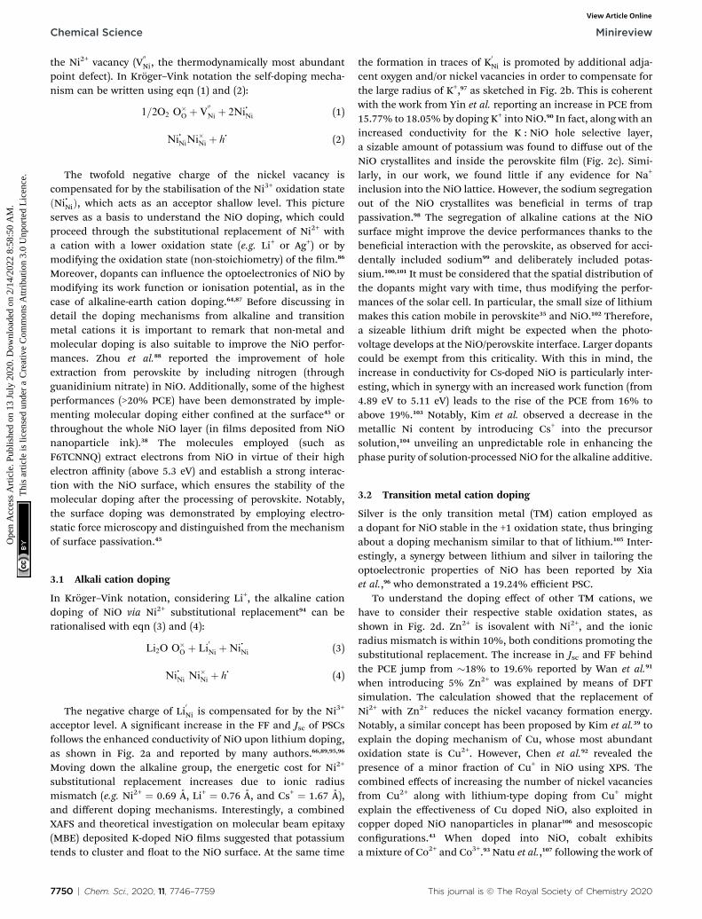
Fig. 1 (a) Publication rate evaluated as the number of papers per month as calculated using the Scopus database for the “NiO” and “perovskitesolar cells” keywords. (b) Record PCE chart for p–i–n perovskite solar cells employing NiO as a hole selective layer. Ref. 36–46: the keyapproaches leading to record efficiency are indicated. (c) Scheme linking the NiO precursor formulation to the critical properties of the final NiOfilms. The effect of the Ni precursor on the surface chemistry is highlighted by XPS investigation (as described in ref. 47) on NiO films processedfrom NiCl2, Ni(NO3)2, Ni(AcO)2 and Ni(acac)2 showing that chloride remains bound to the surface. (d) Example of full inorganic (perovskite andselective layers) PSC configuration. (e) Dependance of the PCE of full inorganic NiO/CsPbI2Br PSCs on the electron selective layer. (f) The bestcell from Fig. 1d with the complete inorganic configuration NiO/CsPbI2Br/ZnO@C60. (e) and (f) are reprinted with permission from ref. 48.Copyright 2018 American Chemical Society.
Chemical Science Minireview
Ope
n A
cces
s A
rtic
le. P
ublis
hed
on 1
3 Ju
ly 2
020.
Dow
nloa
ded
on 2
/14/
2022
8:5
8:50
AM
. T
his
artic
le is
lice
nsed
und
er a
Cre
ativ
e C
omm
ons
Attr
ibut
ion
3.0
Unp
orte
d L
icen
ce.
View Article Online
solar modules at a high technology readiness level (TRL). Withthis aim, the research on cost-effective, scalable, and highthroughput deposition techniques needs to be addressed asa hot topic for the future development of PSC photovoltaictechnology. Considering the whole manufacturing process,necessary actions have to be considered concerning the scalabledeposition of the entire stack forming PSC devices. In this topic,the uniform and scalable deposition of hole transport layersplays an essential role in both n–i–p and p–i–n device archi-tectures. On the other hand, the processing temperature andoperational stability of HSLs have to be taken into account too.
7748 | Chem. Sci., 2020, 11, 7746–7759
NiO offers considerable opportunities to match all theserequirements.
NiO layers have been deposited by well-established indus-trially relevant physical and chemical vapour deposition tech-niques. Techniques like sputtering,64,65 pulsed laser deposition(PLD),66 thermal67 and electron-beam evaporation,68 chemicalvapour deposition (CVD) and atomic layer deposition (ALD)69
have been introduced for the manufacturing of NiO layers forhighly efficient inverted p–i–n perovskite solar cells, approach-ing 20% PCE.68 Whether these techniques could represent theconvenient industrial process for NiO deposition woulddepend, besides the quality of the NiO layer, on the cost and
This journal is © The Royal Society of Chemistry 2020

Minireview Chemical Science
Ope
n A
cces
s A
rtic
le. P
ublis
hed
on 1
3 Ju
ly 2
020.
Dow
nloa
ded
on 2
/14/
2022
8:5
8:50
AM
. T
his
artic
le is
lice
nsed
und
er a
Cre
ativ
e C
omm
ons
Attr
ibut
ion
3.0
Unp
orte
d L
icen
ce.
View Article Online
throughput. Ideally, the use of vacuum-free printing techniquesbased on solution processing might t those requirements.Methods like chemical bath deposition (CBD),70 electrodeposi-tion,42,71 spray pyrolysis,72,73 blade coating and screen-printingare, therefore, highly attractive. At the same time, it could beconvenient to adopt processing routes which can be straight-forwardly implemented into the already operative industrialline. With this in mind, an available and cost-effective solutioncould consist of the deposition of a NiO lm during themanufacturing process of transparent conductive oxides(TCOs). The most commonly used TCOs for PSC technology areindium tin oxide (ITO) and uorine-doped tin oxide (FTO). TheITO coating is generally deposited by sputtering and commer-cially available on both rigid glass and exible plasticsubstrates. FTO is made by spray pyrolysis deposition (SPD) ata high processing temperature limiting its use on glasssubstrates only. Sputtering and SPD are both suitable tech-niques for obtaining a high-quality NiO lm, which makes theintegration of the deposition in the manufacturing process ofTCOs the most advantageous option. Sequential manufacturingof the TCO and the NiO HSL in the same production line canguarantee better reproducibility and a high throughput process.Different is the case of tandem photovoltaics, where the PSCacts as a wide-bandgap device in combination with silicon orCIGS. Mechanically stacking the PCS on top of the silicon solarcell, as shown by Lamanna et al.,74 would directly enable everyNiO deposition demonstrated in the literature. Nonetheless,aiming at processing the PSC on top of a textured silicon solarcell in a monolithic tandem device, sputtering might be an idealtechnique for the deposition of a 15–20 nm thick conformal NiOlayer, as demonstrated by Hou et al. who achieved a certiedPCE of 25.7%.75 Alternatively, Jost et al. employed ALD todeposit NiO on top of a rough CIGSe solar cell, and achieveda 21.6% PCE when introducing a thin PTAA passivation layer toimprove the Voc and ll factor (FF) of the perovskite device.76
2.3 N–i–p perovskite solar cells
Specular to the approach of full inorganic p–i–n perovskite solarcells, the introduction of NiO as a hole selective layer into an n–i–p architecture is one of the most promising routes to stabiliseperovskite photovoltaics. Excellent demonstrations are theCuSCN/rGO hole selective layer developed by Arora et al.,77 andthe 16 months of shelf-life stability by employing NiO and TiO2
as layers in a p–i–n architecture demonstrated by Zhao et al.78
Despite the great promise, few demonstrations of NiO in n–i–p PSCs have been reported to date, all exploiting inks of NiOnanoparticles (NPs) based on solvents orthogonal to perovskitedue to the high temperature needed for the other deposition ofNiO. The standard approach is to produce functionalised NiOnanoparticles, capped with an organic species which allowssolubility in aromatic or alcoholic solvents.79–82 The PCE iswithin 12% and 9%, due to the negative impact of the organicshell on the conductivity of the NiO layers and on the holetransfer from the perovskite. In fact, Liu et al. observed anincrease in PCE in the p–i–n architecture aer removing part ofthe ligands with an UV-ozone treatment,81 a procedure not
This journal is © The Royal Society of Chemistry 2020
compatible with n–i–p devices. Another reason for the relativelypoor performances might be the quality of the NiO lm, interms of NP packing and electrical layer with the perovskite. Tothis end, a ner tuning of the deposition technique, NP size andsize dispersity might enable more efficient layers. An alternativeis to ll the NiO NP lm with an organic or polymeric holeselective layer, as in the case of the NiO|Spiro-OMeTAD bi-layershown by Li et al.,83 who demonstrated a 21.6% efficiency.Moreover, the authors suggest that NiO might act as a protect-ing layer, slowing down the diffusion of Spiro-OMeTAD dopantsinto the perovskite layer, thus stabilising the device.
2.4 Safety hazards
The use of NiO presents some safety concerns due to its toxicity.Nickel itself is suspected of causing cancer, can cause anallergic reaction and may cause damage to organs. The NIOSHsuggests a recommended exposure limit of 0.015 mg m�3 forcontinuous exposure of 8 hours.84 Nickel oxide shows similarhazards; however, the potential exposure when deposited asa well-bonded thin lm can be considered very limited. Themain risk occurs in the deposition phase, raising safetyconcerns for the operators. In a sol–gel synthesis, each nickelprecursor has specic toxicity: while nickel acetate is lessharmful than nickel, nickel nitrate and nickel chloride presentsome additional risks.27 Commonly used solvents like 2-methoxy ethanol, acetylacetone, and ethylene glycol are alsoincreasing the risk if the operator is exposed to the sol–gel inkor its fumes.
Nevertheless, with the appropriate use of personal protectiveequipment (PPE) as well as a conned deposition environment,it is possible to minimise risks. Other solvents such as alcoholsor water can lower the requirements for ventilation, and theiruse should be encouraged. When nanoparticles are used, theirsmaller size and their airborne nature represent a signicantincrease in the risks. Recent studies suggested that the exposurelimit should be 10 times lower than bulk nickel oxide,85 and it isessential to have strict control on the handling of dry nano-powders. For the same reason it is vital to ensure good adhesionwith the substrate (especially on a exible substrate in a roll-to-roll production) to avoid the release of airborne particles. WhenNiO is deposited by sputtering or e-beam evaporation, the lmis usually well bonded to the substrate and the risks are mostlylimited to the periodic cleaning of the chamber or due todeposition of akes from the target on samples. We want toemphasise that it is essential to develop appropriate safetyprocedures when handling this material, both during theresearch and the development phase as well as in the eventualindustrialisation phase. We also believe that with good controlof the thin lm deposition procedure, it is possible to use Niand NiO without risks, as the material is already widely used inthe industry.
3. Doping of NiO
NiO is an insulator in its stoichiometric form, with its p-typeconductivity arising from the self-doping mechanism due to
Chem. Sci., 2020, 11, 7746–7759 | 7749
Chemical Science Minireview
Ope
n A
cces
s A
rtic
le. P
ublis
hed
on 1
3 Ju
ly 2
020.
Dow
nloa
ded
on 2
/14/
2022
8:5
8:50
AM
. T
his
artic
le is
lice
nsed
und
er a
Cre
ativ
e C
omm
ons
Attr
ibut
ion
3.0
Unp
orte
d L
icen
ce.
View Article Online
the Ni2+ vacancy (V00Ni, the thermodynamically most abundant
point defect). In Kroger–Vink notation the self-doping mecha-nism can be written using eqn (1) and (2):
1=2O2 O�O þ V
00Ni þ 2Ni
�
Ni (1)
Ni�
NiNi�Ni þ h�
(2)
The twofold negative charge of the nickel vacancy iscompensated for by the stabilisation of the Ni3+ oxidation stateðNi�NiÞ, which acts as an acceptor shallow level. This pictureserves as a basis to understand the NiO doping, which couldproceed through the substitutional replacement of Ni2+ witha cation with a lower oxidation state (e.g. Li+ or Ag+) or bymodifying the oxidation state (non-stoichiometry) of the lm.86
Moreover, dopants can inuence the optoelectronics of NiO bymodifying its work function or ionisation potential, as in thecase of alkaline-earth cation doping.64,87 Before discussing indetail the doping mechanisms from alkaline and transitionmetal cations it is important to remark that non-metal andmolecular doping is also suitable to improve the NiO perfor-mances. Zhou et al.88 reported the improvement of holeextraction from perovskite by including nitrogen (throughguanidinium nitrate) in NiO. Additionally, some of the highestperformances (>20% PCE) have been demonstrated by imple-menting molecular doping either conned at the surface45 orthroughout the whole NiO layer (in lms deposited from NiOnanoparticle ink).38 The molecules employed (such asF6TCNNQ) extract electrons from NiO in virtue of their highelectron affinity (above 5.3 eV) and establish a strong interac-tion with the NiO surface, which ensures the stability of themolecular doping aer the processing of perovskite. Notably,the surface doping was demonstrated by employing electro-static force microscopy and distinguished from the mechanismof surface passivation.45
3.1 Alkali cation doping
In Kroger–Vink notation, considering Li+, the alkaline cationdoping of NiO via Ni2+ substitutional replacement94 can berationalised with eqn (3) and (4):
Li2O O�O þ Li
0Ni þNi
�
Ni (3)
Ni�
Ni Ni�Ni þ h�
(4)
The negative charge of Li0Ni is compensated for by the Ni3+
acceptor level. A signicant increase in the FF and Jsc of PSCsfollows the enhanced conductivity of NiO upon lithium doping,as shown in Fig. 2a and reported by many authors.66,89,95,96
Moving down the alkaline group, the energetic cost for Ni2+
substitutional replacement increases due to ionic radiusmismatch (e.g. Ni2+ ¼ 0.69 A, Li+ ¼ 0.76 A, and Cs+ ¼ 1.67 A),and different doping mechanisms. Interestingly, a combinedXAFS and theoretical investigation on molecular beam epitaxy(MBE) deposited K-doped NiO lms suggested that potassiumtends to cluster and oat to the NiO surface. At the same time
7750 | Chem. Sci., 2020, 11, 7746–7759
the formation in traces of K0Ni is promoted by additional adja-
cent oxygen and/or nickel vacancies in order to compensate forthe large radius of K+,97 as sketched in Fig. 2b. This is coherentwith the work from Yin et al. reporting an increase in PCE from15.77% to 18.05% by doping K+ into NiO.90 In fact, along with anincreased conductivity for the K : NiO hole selective layer,a sizable amount of potassium was found to diffuse out of theNiO crystallites and inside the perovskite lm (Fig. 2c). Simi-larly, in our work, we found little if any evidence for Na+
inclusion into the NiO lattice. However, the sodium segregationout of the NiO crystallites was benecial in terms of trappassivation.98 The segregation of alkaline cations at the NiOsurface might improve the device performances thanks to thebenecial interaction with the perovskite, as observed for acci-dentally included sodium99 and deliberately included potas-sium.100,101 It must be considered that the spatial distribution ofthe dopants might vary with time, thus modifying the perfor-mances of the solar cell. In particular, the small size of lithiummakes this cation mobile in perovskite35 and NiO.102 Therefore,a sizeable lithium dri might be expected when the photo-voltage develops at the NiO/perovskite interface. Larger dopantscould be exempt from this criticality. With this in mind, theincrease in conductivity for Cs-doped NiO is particularly inter-esting, which in synergy with an increased work function (from4.89 eV to 5.11 eV) leads to the rise of the PCE from 16% toabove 19%.103 Notably, Kim et al. observed a decrease in themetallic Ni content by introducing Cs+ into the precursorsolution,104 unveiling an unpredictable role in enhancing thephase purity of solution-processed NiO for the alkaline additive.
3.2 Transition metal cation doping
Silver is the only transition metal (TM) cation employed asa dopant for NiO stable in the +1 oxidation state, thus bringingabout a doping mechanism similar to that of lithium.105 Inter-estingly, a synergy between lithium and silver in tailoring theoptoelectronic properties of NiO has been reported by Xiaet al.,96 who demonstrated a 19.24% efficient PSC.
To understand the doping effect of other TM cations, wehave to consider their respective stable oxidation states, asshown in Fig. 2d. Zn2+ is isovalent with Ni2+, and the ionicradius mismatch is within 10%, both conditions promoting thesubstitutional replacement. The increase in Jsc and FF behindthe PCE jump from �18% to 19.6% reported by Wan et al.91
when introducing 5% Zn2+ was explained by means of DFTsimulation. The calculation showed that the replacement ofNi2+ with Zn2+ reduces the nickel vacancy formation energy.Notably, a similar concept has been proposed by Kim et al.39 toexplain the doping mechanism of Cu, whose most abundantoxidation state is Cu2+. However, Chen et al.92 revealed thepresence of a minor fraction of Cu+ in NiO using XPS. Thecombined effects of increasing the number of nickel vacanciesfrom Cu2+ along with lithium-type doping from Cu+ mightexplain the effectiveness of Cu doped NiO, also exploited incopper doped NiO nanoparticles in planar106 and mesoscopiccongurations.43 When doped into NiO, cobalt exhibitsa mixture of Co2+ and Co3+.93 Natu et al.,107 following the work of
This journal is © The Royal Society of Chemistry 2020
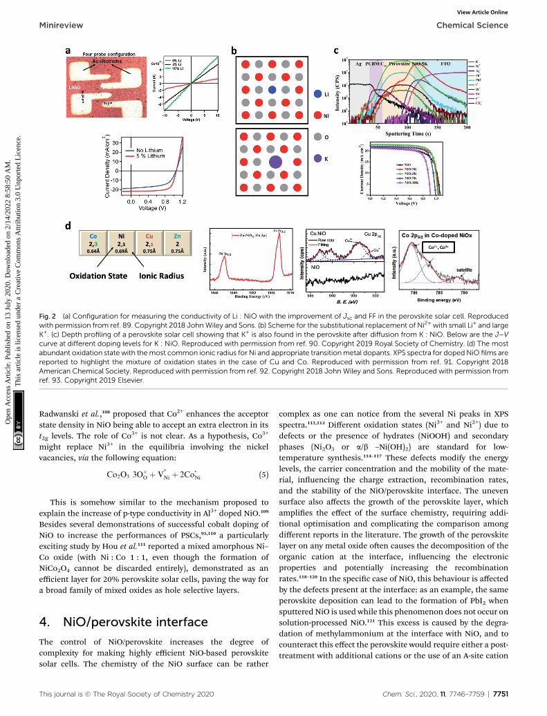
Fig. 2 (a) Configuration for measuring the conductivity of Li : NiO with the improvement of Jsc and FF in the perovskite solar cell. Reproducedwith permission from ref. 89. Copyright 2018 JohnWiley and Sons. (b) Scheme for the substitutional replacement of Ni2+ with small Li+ and largeK+. (c) Depth profiling of a perovskite solar cell showing that K+ is also found in the perovskite after diffusion from K : NiO. Below are the J–Vcurve at different doping levels for K : NiO. Reproduced with permission from ref. 90. Copyright 2019 Royal Society of Chemistry. (d) The mostabundant oxidation state with themost common ionic radius for Ni and appropriate transitionmetal dopants. XPS spectra for dopedNiO films arereported to highlight the mixture of oxidation states in the case of Cu and Co. Reproduced with permission from ref. 91. Copyright 2018American Chemical Society. Reproduced with permission from ref. 92. Copyright 2018 John Wiley and Sons. Reproduced with permission fromref. 93. Copyright 2019 Elsevier.
Minireview Chemical Science
Ope
n A
cces
s A
rtic
le. P
ublis
hed
on 1
3 Ju
ly 2
020.
Dow
nloa
ded
on 2
/14/
2022
8:5
8:50
AM
. T
his
artic
le is
lice
nsed
und
er a
Cre
ativ
e C
omm
ons
Attr
ibut
ion
3.0
Unp
orte
d L
icen
ce.
View Article Online
Radwanski et al.,108 proposed that Co2+ enhances the acceptorstate density in NiO being able to accept an extra electron in itst2g levels. The role of Co3+ is not clear. As a hypothesis, Co3+
might replace Ni3+ in the equilibria involving the nickelvacancies, via the following equation:
Co2O3 3O�O þ V
00Ni þ 2Co
�
Ni (5)
This is somehow similar to the mechanism proposed toexplain the increase of p-type conductivity in Al3+ doped NiO.109
Besides several demonstrations of successful cobalt doping ofNiO to increase the performances of PSCs,95,110 a particularlyexciting study by Hou et al.111 reported a mixed amorphous Ni–Co oxide (with Ni : Co 1 : 1, even though the formation ofNiCo2O4 cannot be discarded entirely), demonstrated as anefficient layer for 20% perovskite solar cells, paving the way fora broad family of mixed oxides as hole selective layers.
4. NiO/perovskite interface
The control of NiO/perovskite increases the degree ofcomplexity for making highly efficient NiO-based perovskitesolar cells. The chemistry of the NiO surface can be rather
This journal is © The Royal Society of Chemistry 2020
complex as one can notice from the several Ni peaks in XPSspectra.112,113 Different oxidation states (Ni3+ and Ni2+) due todefects or the presence of hydrates (NiOOH) and secondaryphases (Ni2O3 or a/b –Ni(OH)2) are standard for low-temperature synthesis.114–117 These defects modify the energylevels, the carrier concentration and the mobility of the mate-rial, inuencing the charge extraction, recombination rates,and the stability of the NiO/perovskite interface. The unevensurface also affects the growth of the perovskite layer, whichamplies the effect of the surface chemistry, requiring addi-tional optimisation and complicating the comparison amongdifferent reports in the literature. The growth of the perovskitelayer on any metal oxide oen causes the decomposition of theorganic cation at the interface, inuencing the electronicproperties and potentially increasing the recombinationrates.118–120 In the specic case of NiO, this behaviour is affectedby the defects present at the interface: as an example, the sameperovskite deposition can lead to the formation of PbI2 whensputtered NiO is used while this phenomenon does not occur onsolution-processed NiO.121 This excess is caused by the degra-dation of methylammonium at the interface with NiO, and tocounteract this effect the perovskite would require either a post-treatment with additional cations or the use of an A-site cation
Chem. Sci., 2020, 11, 7746–7759 | 7751

Chemical Science Minireview
Ope
n A
cces
s A
rtic
le. P
ublis
hed
on 1
3 Ju
ly 2
020.
Dow
nloa
ded
on 2
/14/
2022
8:5
8:50
AM
. T
his
artic
le is
lice
nsed
und
er a
Cre
ativ
e C
omm
ons
Attr
ibut
ion
3.0
Unp
orte
d L
icen
ce.
View Article Online
excess in ink. Alternative deposition techniques such as the hot-casting method seem less prone to give rise to defects at theinterface.89 These phenomena show that improvement in theenergy alignment and reduction in defects during the perov-skite growth can be achieved not only by modifying thesynthesis of NiO but also by tailoring the perovskite deposition.
4.1 Charge dynamics at the NiO/perovskite interface
From a fundamental point of view, the NiO interface can extractholes in times down to the sub-picosecond scale, and the widebandgap allows slowing down the recombination to the order ofhundreds of picoseconds.122 For these reasons, the interface isnot considered a limiting factor in the hole extraction whencompared to PEDOT.123 However, the NiO interface can havea large number of defects. Defect engineering has been widelyapplied to improve the performance of NiO based devices,either by tuning the concentration of Ni3+ or by inducing theformation of additional NiOOH.124–127 Increasing the Ni3+
concentration can improve conductivity and charge transfer,but at the same time, it causes non-negligible parasiticabsorption.125,128 The proper use of NiOOH also appear complexdue to the very different energetic levels at the different crys-talline surfaces.129 Extrinsic doping seems like a more prom-ising approach because it allows tuning of the conductivity,work function and bandgap without the optical losses due toNi3+. The presence of Ni3+ sites at the interface is also notrequired for the extraction of charges since there is evidencethat holes are transferred to the Ni2+ sites.130
4.2 NiO/perovskite interface stability
Perovskite solar cells with NiO are usually considered to be verystable, with several reports showing high stability under light(with UV) and thermal stresses that would allow passing severalIEC tests.68,135–137 The main reason is the structural stability ofthe NiO layer, preventing the layer of perovskite with the elec-trodes. Nevertheless, the NiO/perovskite interface can showsome specic degradationmechanism that should be preventedto fabricate stable devices. In particular, the formation of NiI2has been detected upon thermal degradation of the NiO/perovskite interface.132,133 The process is triggered by the largenegative enthalpy of the NiO reaction with HI, arising fromMAI(Fig. 3b).132 Under electrical bias, the interaction between NiOand iodide can result in redox reactions, which can explain theJ–V hysteresis and impact the interface stability (Fig. 3e).124
Light soaking might be benecial for improving the perovskitecrystallinity138 or either induce interface degradation to NiI2(Fig. 3c)139 or PbI2 (Fig. 3a).131 The formation of an oxygen-containing perovskite interphase (CH3NH3PbI3�2xOx, Fig. 3d)has been proposed as well, which can not only induce interfa-cial p-doping, but also open a new pathway towards degrada-tion.134 It is worth noting that the reports on light soaking testsbeyond 1000 hours employ inks with a stoichiometric compo-sition of cations and anions, so preventing the formation ofPbI2 could help to improve the durability of the interface.135
Other solutions are the use of hybrid interlayers such asmagnesium acetate or ionic liquids such as 1-butyl-3-
7752 | Chem. Sci., 2020, 11, 7746–7759
methylimidazolium tetrauoroborate to enhance the interfacebetween NiO and perovskite, with enhancements in bothperformance and stability.124,135 In particular, the former canimprove the NiO interface electrical stability while the latter isuseful to prevent the segregation of halides.
4.3 NiO functionalisation
Surface treatments with oxygen plasma or UV/O3 can be a validapproach tomodify the surface of a metal oxide. Still, the resultsin perovskite solar cells are not consolidated and are, probably,strongly dependent on the starting conditions (the type of NiOand the perovskite synthesis).124,140 The functionalisation of theNiO surface appears more suitable to achieve reproducibleimprovements and to be less sensitive to the synthesis of NiO. Adouble layer is also oen used in efficient OLEDs to differen-tiate the function of selective transport and charge injection,and a similar approach could be used here for hole extractionand electron blocking. The functionalisation of NiO can beachieved with inorganic,46 hybrid124 or organiccompounds.45,118,120,141–145 We believe that this approach will bekey to maximising the performance of PSCs with NiO. Forinstance, the introduction of a thin PTAA coating on NiOreduces the interface recombination120 and a similar effect hasbeen observed with alternative polymers146 or by treating theNiO surface with different alkali halides: KCl,46 NaCl98 orCsBr.147 Another possibility is to gra self-assembled mono-layers (SAMs) on the NiO surface, by bonding throughamines,118 carboxylates142 and thiols148 with phosphonic acidalso potentially effective. An organic interlayer, also exploitingthe versatility due to the tunable molecular structure (especiallyin the case of SAMs), could tackle different issues such as thecontrol of the surface chemistry, defect-free growth of perov-skite, reduction of mechanical stress, and formation of covalentbonding. In this way, it will be possible to stabilise the interface,promote an appropriate growth of the perovskite and improvethe VOC of p–i–n solar cells to achieve efficiencies on par with n–i–p devices.
5. Broad application of NiO inperovskite photovoltaics
Perovskite photovoltaics is attractive for a broad range ofapplications. Low-temperature processing is compatible withexible substrates. In combination with the excellent perfor-mances under indoor lighting,149 this could have a signicantimpact on the IoT (Internet of Things). Additionally, the lowcosts can be further abated by printing the counter electrode.Especially when considering consumer electronics and wear-ables the chance to go lead-free is of paramountimportance.150,151
5.1 Flexible perovskite solar cells
Plastic substrates limit the processing temperature to below150 �C.154 This makes the NiO nanoparticle ink route the solecompatible solution process.54,155 Doping NiO nanoparticles inexible PSCs boosts the efficiency from around 13% (undoped
This journal is © The Royal Society of Chemistry 2020

Fig. 3 (a) The formation of PbI2 at NiO/CH3NH3PbI3 upon light irradiation and the effect on charge transport. Readapted with permission fromref. 131. Copyright 2018 Royal Society of Chemistry. (b) Reaction enthalpies for the decomposition of methylammonium iodide on the NiOsurface. Reproduced with permission from ref. 132. Copyright 2020 American Chemical Society. (c) XRD spectra of NiO exposed to methyl-ammonium iodide solution at increasing temperature showing the formation of NiI2. Readapted with permission from ref. 133. Copyright 2019American Chemical Society. (d) Scheme for the formation of an oxygen-containing perovskite at the NiO interface. Reproduced with permissionfrom ref. 134. Copyright 2016 John Wiley and Sons. (e) Scheme for redox chemistry at the NiO/perovskite interface. Readapted with permissionfrom ref. 124. Copyright 2019 John Wiley and Sons.
Minireview Chemical Science
Ope
n A
cces
s A
rtic
le. P
ublis
hed
on 1
3 Ju
ly 2
020.
Dow
nloa
ded
on 2
/14/
2022
8:5
8:50
AM
. T
his
artic
le is
lice
nsed
und
er a
Cre
ativ
e C
omm
ons
Attr
ibut
ion
3.0
Unp
orte
d L
icen
ce.
View Article Online
NiO)54,155 to above 16% with Cu : NiO106 and to 14.5% withFe : NiO.156 A remarkable increase to 20% PCE has been ach-ieved with the molecular dopant F2HCNQ.38 Excellent opera-tional stabilities (>90% PCE aer 500 h of MPPT) have beendemonstrated combining a PCBM/ZnO electron selective layerand the NiO NP layer.157 A minor loss of efficiency aer 1000bending cycles at a radius of 5–8 mm was also demon-strated.38,106,157 2-D materials might be particularly well suitedfor exible electronics, thanks to their electrical and mechan-ical properties.158 In particular, graphene quantum dot (GQD)doping of the NiO NP layer has risen to prominence because italso allows us to explore different functionalisation of the 2Dmaterial.159 For instance, Zhang et al.160 showed an improve-ment in PCE from 14.6% to above 18% on a rigid device bychemically reducing the graphene oxide dopant with hydrazineor urea, also demonstrating a 14.1% PCE on a plastic substrate.Wang et al.161 investigated in detail the effect of the function-alising group, nding that hydroxy-functionalised GQDsinduced a severe aggregation of the NiO nanoparticles within
This journal is © The Royal Society of Chemistry 2020
the precursor ink. At the same time, the amine functionalisa-tion enabled the formation of a smooth and high-quality NiOlayer leading to a PCE of 19.55% on a rigid substrate and ofabove 18% on PEN/ITO and maintaining 88% of PCE aer 1000bending cycles at a diameter of 10 mm. Further investigation onthe effect of functionalised GQDs on the mechanical stability ofexible devices will be of high interest to consolidate this crit-ical approach. An insightful analysis about the mechanicalstability is provided by Cong et al.,152 who exploited e-beamevaporation with a glazing-angle atomic deposition layout(GLAD) to control the morphology of the NiO layer (Fig. 4a). Theprocess is compatible with plastic substrates, and by varying theglancing angle it is possible to cast a compact layer (GA ¼ 0�) ora nanopillar array (GA ¼ 85�). The optimised nanopillar arrayincreased the Jsc and the FF of the solar cells, and exibledevices with PCE above 17% were demonstrated. Moreover,nite element simulation showed that the presence of thenanopillar array on top of the compact layer reduced the
Chem. Sci., 2020, 11, 7746–7759 | 7753

Fig. 4 (a) Morphology and hole transfer mechanism for the NiO nanopillar array as discussed in ref. 152. (b) Finite element simulation showingthe lower stress for the nanopillar array NiO layer, from ref. 152. (a) and (b) Reproduced with permission from ref. 152. Copyright 2019 AmericanChemical Society. (c) Device architecture, J–V curve and IPCE for a 10% efficient lead-free perovskite solar cell employing NiO as the holeselective layer. Reproduced with permission from ref. 153. Copyright 2018 Elsevier.
Chemical Science Minireview
Ope
n A
cces
s A
rtic
le. P
ublis
hed
on 1
3 Ju
ly 2
020.
Dow
nloa
ded
on 2
/14/
2022
8:5
8:50
AM
. T
his
artic
le is
lice
nsed
und
er a
Cre
ativ
e C
omm
ons
Attr
ibut
ion
3.0
Unp
orte
d L
icen
ce.
View Article Online
mechanical stress upon bending (Fig. 4b), directly improvingthe mechanical stability of exible perovskite solar cells.
5.2 Carbon-based printable perovskite solar cells
Triple mesoscopic stack perovskite solar cells with a printablecarbon electrode (c-PSCs) are a subject of intense research dueto their low cost and promising stability, especially whenintroducing 5-AVA into the perovskite composition.162 In c-PSCs, the perovskite is inltrated through mp-TiO2 as an elec-tron selective layer and a mesoporous Al2O3 or ZrO2 scaffold.The electrode is printed carbon, which guarantees higherstability concerning metal electrodes and partially acts as anencapsulating layer. The efficiency of HTM-free c-PSCs, which isthe standard conguration, with the carbon electrode alsofunctioning as a hole layer, is severely hindered by the low Vocand FF. This drawback can be mitigated by introducing a p-typelayer.163 Xu et al.164 observed a net increase in both Jsc (from 14.3mA cm�2 to 21.3 mA cm�2) and Voc (from 0.66 V to 0.76 V) whenexploiting multiple mp-TiO2/mp-ZrO2/mp-NiO and a PCEapproaching 15%. Improved energetic alignment betweenperovskite and a NiO containing carbon electrode might explainthe PCE.165–167 Intensive research was aer that dedicated toimproving the efficiency of c-PSCs by modifying the NiO layermorphology,168 processing169,170 or doping.171 Still, more work isrequired to improve the PCE from about 15% substantially.However, efficiencies above 18% employing printable carbonelectrodes have been demonstrated by adopting an n–i–pconguration with P3HT/graphene172 or CuSCN173 as a compactHSL on top of the perovskite, suggesting that future advance-ment in NiO processing on top of perovskites could enable
7754 | Chem. Sci., 2020, 11, 7746–7759
stable and cheap carbon-based perovskite solar cells withminimal efficiency losses.
5.3 Lead-free perovskite solar cells
Lead-free perovskite solar cells with high efficiency are now onlya matter of time, as conrmed by the certied efficiency of12.4%.174 It is interesting to note that PEDOT:PSS is the mostemployed HSL for Sn-based PSCs.175 With lead halide perov-skites, one of the driving forces to adopt NiO was the replace-ment of the relatively unstable PEDOT:PSS.176,177 The reasonsbehind the scarce application of NiO in Sn–PSCs are not known.The prime suspect is that the lower ionisation energy ofPEDOT:PSS with respect to NiO might drive a better bandalinement with the VB of tin halide perovskites, shallower thanthe Pb counterpart. Another possibility is that the NiOOH-richsurface might induce Sn2+ oxidation to Sn4+, degrading theinterface. Ideally, these two issues might be tackled via interfaceengineering. The valence band of NiO can be shied byanchoring molecular dipoles on the surface.143
Moreover, molecular monolayers have been proved excellentto protect perovskite surfaces and interfaces.178 We foresee thatchemical or physical treatments of the NiO surface179,180 mightalso improve the optoelectronic quality of the NiO/Sn–perov-skite interface. For instance, NaBH4 has been proved effective inreducing the NiO surface.181 This specic research topic is in itsinfancy, and still pioneering results push towards cautiousoptimism. A 3.31% efficient b-CsSnI3 PSC employing a sput-tered-NiO/spin-coated NiO bi-layer was demonstrated by Wanget al.182 and an efficiency approaching 10% was obtained by Liet al.183 and Wang et al.153 (Fig. 4c).
This journal is © The Royal Society of Chemistry 2020
Minireview Chemical Science
Ope
n A
cces
s A
rtic
le. P
ublis
hed
on 1
3 Ju
ly 2
020.
Dow
nloa
ded
on 2
/14/
2022
8:5
8:50
AM
. T
his
artic
le is
lice
nsed
und
er a
Cre
ativ
e C
omm
ons
Attr
ibut
ion
3.0
Unp
orte
d L
icen
ce.
View Article Online
6. Conclusion and outlook
The implementation of NiO as a hole selective layer in halideperovskite photovoltaics yields power conversion efficienciesabove 20%, together with low cost, easy processing and longterm stability. NiO nanoparticles will probably be the choice ofmaterial for exible photovoltaics. Here, the synergy with 2Dmaterials can be particularly fruitful by improving mechanicalexibility and reducing energy losses. When considering rigidsubstrates and tandem photovoltaics, processing by sputteringor spray pyrolysis might be the best choice for easy industrialadoption, with the TCO/NiO substrate processed in the sameline. We have discussed in detail that a broad set of dopants canbe introduced to enhance the conductivity of NiO or to improvethe energy level alinement with halide perovskites. We haveshown that each dopant acts in a different way depending on itssize, valence and chemical identity. In our opinion a denitivechoice of the best NiO dopant is not possible yet, especiallyconsidering the long term stability and the variety of perovskiteformulations that can be used. Dopants can segregate at the NiOsurface or diffuse inside the perovskite, and the doping stabilityhas to be assessed in greater detail. In addition to that, weshowed that pieces of evidence are accumulating stressing thatNiO is particularly reactive for lead halide perovskites. Light,temperature and electrical bias can all trigger the NiO/perovskitereactivity. Thus, aiming at highly efficient and stable solar cells,the introduction of a passivation layer seems mandatory. Self-assembled monolayers can represent an ideal choice topassivate NiO defects, tuning the energy levels and promotingthe growth of a high-quality perovskite lm. An alternative mightbe the introduction of an ultra-thin layer (tunnelling layer) ofinorganic insulating materials (e.g. MgO and Al2O3). Moreover,we believe that careful engineering of the NiO surface will enableefficient and stable lead-free perovskite solar cells.
Conflicts of interest
There are no conicts to declare.
Acknowledgements
D.D.G. acknowledges the PhD program of the Department ofChemistry of La Sapienza University of Rome for funding. D.D.acknowledges the nancial support from MIUR (Project PRIN2017 with title: Novel Multilayered and Micro-Machined Elec-trode Nano-Architectures for Electrocatalytic Applications- Prot.2017YH9MRK). D.D. also acknowledges the nancial supportfrom the University of Rome LA SAPIENZA [Project ATENEO2019 Prot.RM11916B756961CA].
References
1 J.-P. Correa-Baena, A. Abate, M. Saliba, W. Tress, T. JesperJacobsson, M. Gratzel and A. Hagfeldt, Energy Environ.Sci., 2017, 10, 710–727.
2 M. Gratzel, Nat. Mater., 2014, 13, 838–842.3 H. J. Snaith, J. Phys. Chem. Lett., 2013, 4, 3623–3630.
This journal is © The Royal Society of Chemistry 2020
4 NREL Best Research-Cell Efficiencies, https://www.nrel.gov/pv/assets/pdfs/pv-efficiencies, accessed 19 November 2018.
5 P. Schulz, ACS Energy Lett., 2018, 3, 1287–1293.6 S. Ravishankar, S. Gharibzadeh, C. Roldan-Carmona,G. Grancini, Y. Lee, M. Ralaiarisoa, A. M. Asiri, N. Koch,J. Bisquert and M. K. Nazeeruddin, Joule, 2018, 2, 788–798.
7 M. Stolterfoht, C.M.Wolff, J. A. Marquez, S. Zhang, C. J. Hages,D. Rothhardt, S. Albrecht, P. L. Burn, P.Meredith, T. Unold andD. Neher, Nat. Energy, 2018, 3, 847–854.
8 I. Gelmetti, N. F. Montcada, A. Perez-Rodrıguez, E. Barrena,C. Ocal, I. Garcıa-Benito, A. Molina-Ontoria, N. Martın,A. Vidal-Ferran and E. Palomares, Energy Environ. Sci.,2019, 12, 1309–1316.
9 E. H. Anaraki, A. Kermanpur, L. Steier, K. Domanski,T. Matsui, W. Tress, M. Saliba, A. Abate, M. Gratzel,A. Hagfeldt and J.-P. Correa-Baena, Energy Environ. Sci.,2016, 9, 3128–3134.
10 E. Calabro, F. Matteocci, A. L. Palma, L. Vesce, B. Taheri,L. Carlini, I. Pis, S. Nappini, J. Dagar, C. Battocchio,T. M. Brown and A. Di Carlo, Sol. Energy Mater. Sol. Cells,2018, 185, 136–144.
11 A. Kojima, K. Teshima, Y. Shirai and T. Miyasaka, J. Am.Chem. Soc., 2009, 131, 6050–6051.
12 J. J. Yoo, S. Wieghold, M. C. Sponseller, M. R. Chua,S. N. Bertram, N. T. P. Hartono, J. S. Tresback,E. C. Hansen, J.-P. Correa-Baena, V. Bulovic,T. Buonassisi, S. S. Shin and M. G. Bawendi, EnergyEnviron. Sci., 2019, 12, 2192–2199.
13 J. H. Heo, H. J. Han, D. Kim, T. K. Ahn and S. H. Im, EnergyEnviron. Sci., 2015, 8, 1602–1608.
14 T. Gatti, E. Menna, M. Meneghetti, M. Maggini, A. Petrozzaand F. Lamberti, Nano Energy, 2017, 41, 84–100.
15 A. Al-Ashouri, A. Magomedov, M. Roß, M. Jost, M. Talaikis,G. Chistiakova, T. Bertram, J. A. Marquez, E. Kohnen,E. Kasparavicius, S. Levcenco, L. Gil-Escrig, C. J. Hages,R. Schlatmann, B. Rech, T. Malinauskas, T. Unold,C. A. Kaufmann, L. Korte, G. Niaura, V. Getautis andS. Albrecht, Energy Environ. Sci., 2019, 12, 3356–3369.
16 E. H. Jung, N. J. Jeon, E. Y. Park, C. S. Moon, T. J. Shin,T.-Y. Yang, J. H. Noh and J. Seo, Nature, 2019, 567, 511–515.
17 N. J. Jeon, H. Na, E. H. Jung, T.-Y. Yang, Y. G. Lee, G. Kim,H.-W. Shin, S. Il Seok, J. Lee and J. Seo, Nat. Energy, 2018, 3,682–689.
18 A. Abate, D. R. Staff, D. J. Hollman, H. J. Snaith andA. B. Walker, Phys. Chem. Chem. Phys., 2014, 16, 1132–1138.
19 A. Abate, D. J. Hollman, J. Teuscher, S. Pathak, R. Avolio,G. D'Errico, G. Vitiello, S. Fantacci and H. J. Snaith, J. Am.Chem. Soc., 2013, 135, 13538–13548.
20 Q. Wang, C. Bi and J. Huang, Nano Energy, 2015, 15, 275–280.
21 M. Saliba, T. Matsui, J. Y. Seo, K. Domanski, J. P. Correa-Baena, M. K. Nazeeruddin, S. M. Zakeeruddin, W. Tress,A. Abate, A. Hagfeldt and M. Gratzel, Energy Environ. Sci.,2016, 9, 1989–1997.
22 M. Saliba, S. Orlandi, T. Matsui, S. Aghazada, M. Cavazzini,J. P. Correa-Baena, P. Gao, R. Scopelliti, E. Mosconi,K. H. Dahmen, F. De Angelis, A. Abate, A. Hagfeldt,
Chem. Sci., 2020, 11, 7746–7759 | 7755
Chemical Science Minireview
Ope
n A
cces
s A
rtic
le. P
ublis
hed
on 1
3 Ju
ly 2
020.
Dow
nloa
ded
on 2
/14/
2022
8:5
8:50
AM
. T
his
artic
le is
lice
nsed
und
er a
Cre
ativ
e C
omm
ons
Attr
ibut
ion
3.0
Unp
orte
d L
icen
ce.
View Article Online
G. Pozzi, M. Graetzel and M. K. Nazeeruddin, Nat. Energy,2016, 1, 1–7.
23 Y. Kim, E. H. Jung, G. Kim, D. Kim, B. J. Kim and J. Seo, Adv.Energy Mater., 2018, 8, 1–9.
24 R. Singh, P. K. Singh, B. Bhattacharya and H. W. Rhee, Appl.Mater. Today, 2019, 14, 175–200.
25 S. Sajid, A. M. Elseman, H. Huang, J. Ji, S. Dou, H. Jiang,X. Liu, D. Wei, P. Cui and M. Li, Nano Energy, 2018, 51,408–424.
26 X. Yin, Y. Guo, H. Xie, W. Que and L. B. Kong, Sol. RRL,2019, 3, 1900001.
27 Italy|Sigma-Aldrich, https://www.sigmaaldrich.com/italy.html, accessed 13 May 2020.
28 S. Cacovich, L. Cina, F. Matteocci, G. Divitini, P. A. Midgley,A. Di Carlo and C. Ducati, Nanoscale, 2017, 9, 4700–4706.
29 K. Domanski, J. P. Correa-Baena, N. Mine,M. K. Nazeeruddin, A. Abate, M. Saliba, W. Tress,A. Hagfeldt and M. Gratzel, ACS Nano, 2016, 10, 6306–6314.
30 G. Kakavelakis, I. Paradisanos, B. Paci, A. Generosi,M. Papachatzakis, T. Maksudov, L. Naja, A. E. Del RioCastillo, G. Kioseoglou, E. Stratakis, F. Bonaccorso andE. Kymakis, Adv. Energy Mater., 2018, 8, 1702287.
31 S. Wu, R. Chen, S. Zhang, B. H. Babu, Y. Yue, H. Zhu,Z. Yang, C. Chen, W. Chen, Y. Huang, S. Fang, T. Liu,L. Han and W. Chen, Nat. Commun., 2019, 10, 1161.
32 F. Fu, S. Pisoni, Q. Jeangros, J. Sastre-Pellicer, M. Kawecki,A. Paracchino, T. Moser, J. Werner, C. Andres,L. Duchene, P. Fiala, M. Rawlence, S. Nicolay, C. Ballif,A. N. Tiwari and S. Buecheler, Energy Environ. Sci., 2019,12, 3074–3088.
33 J. P. Bastos, U. W. Paetzold, R. Gehlhaar, W. Qiu, D. Cheyns,S. Surana, V. Spampinato, T. Aernouts and J. Poortmans,Adv. Energy Mater., 2018, 8, 1–9.
34 A. Magomedov, E. Kasparavicius, K. Rakstys, S. Paek,N. Gasilova, K. Genevicius, G. Juska, T. Malinauskas,M. K. Nazeeruddin and V. Getautis, J. Mater. Chem. C,2018, 6, 8874–8878.
35 N. Vicente, D. Bresser, S. Passerini and G. Garcia-Belmonte,ChemElectroChem, 2019, 6, 456–460.
36 K. C. Wang, J. Y. Jeng, P. S. Shen, Y. C. Chang, E. W. G. Diau,C. H. Tsai, T. Y. Chao, H. C. Hsu, P. Y. Lin, P. Chen,T. F. Guo and T. C. Wen, Sci. Rep., 2014, 4, 1–8.
37 K. Wang, P. Shen, M. Li, S. Chen, M. Lin, P. Chen andT. Guo, ACS Appl. Mater. Interfaces, 2014, 6, 11851–11858.
38 P. Ru, E. Bi, Y. Zhang, Y. Wang, W. Kong, Y. Sha, W. Tang,P. Zhang, Y. Wu, W. Chen, X. Yang, H. Chen and L. Han,Adv. Energy Mater., 2020, 1903487.
39 J. H. Kim, P. W. Liang, S. T. Williams, N. Cho, C. C. Chueh,M. S. Glaz, D. S. Ginger and A. K. Y. Jen, Adv. Mater., 2015,27, 695–701.
40 J. H. Park, J. Seo, S. Park, S. S. Shin, Y. C. Kim, N. J. Jeon,H.-W. Shin, T. K. Ahn, J. H. Noh, S. C. Yoon, C. S. Hwangand S. Il Seok, Adv. Mater., 2015, 27, 4013–4019.
41 W. Chen, Y. Wu, Y. Yue, J. Liu, W. Zhang, X. Yang, H. Chen,E. Bi, I. Ashraful, M. Gratzel and L. Han, Science, 2015, 350,944–948.
7756 | Chem. Sci., 2020, 11, 7746–7759
42 I. J. Park, G. Kang, M. A. Park, J. S. Kim, S. W. Seo,D. H. Kim, K. Zhu, T. Park and J. Y. Kim, ChemSusChem,2017, 10, 2660–2667.
43 K. Yao, F. Li, Q. He, X. Wang, Y. Jiang, H. Huang andA. K. Y. Jen, Nano Energy, 2017, 40, 155–162.
44 S. Yue, K. Liu, R. Xu, M. Li, M. Azam, K. Ren, J. Liu, Y. Sun,Z. Wang, D. Cao, X. Yan, S. Qu, Y. Lei and Z. Wang, EnergyEnviron. Sci., 2017, 10, 2570–2578.
45 W. Chen, Y. Zhou, L. Wang, Y. Wu, B. Tu, B. Yu, F. Liu,H.-W. Tam, G. Wang, A. B. Djurisic, L. Huang and Z. He,Adv. Mater., 2018, 30, 1800515.
46 W. Chen, Y. Zhou, G. Chen, Y. Wu, B. Tu, F. Liu, L. Huang,A. M. C. Ng, A. B. Djurisic and Z. He, Adv. Energy Mater.,2019, 9, 1803872.
47 D. Di Girolamo, M. Piccinni, F. Matteocci, A. G. Marrani,R. Zanoni and D. Dini, Electrochim. Acta, 2019, 319, 175–184.
48 C. Liu, W. Li, C. Zhang, Y. Ma, J. Fan and Y. Mai, J. Am.Chem. Soc., 2018, 140, 3825–3828.
49 M. Li, C. Zhao, Z.-K. Wang, C.-C. Zhang, H. K. H. Lee,A. Pockett, J. Barbe, W. C. Tsoi, Y.-G. Yang, M. J. Carnie,X.-Y. Gao, W.-X. Yang, J. R. Durrant, L.-S. Liao andS. M. Jain, Adv. Energy Mater., 2018, 8, 1801509.
50 Z. Liu, J. Chang, Z. Lin, L. Zhou, Z. Yang, D. Chen, C. Zhang,S. F. Liu and Y. Hao, Adv. Energy Mater., 2018, 1703432, 1–9.
51 J. W. Jung, C. C. Chueh and A. K. Y. Jen, Adv. Mater., 2015,27, 7874–7880.
52 H. Tan, A. Jain, O. Voznyy, X. Lan, F. P. G. De Arquer,J. Z. Fan, R. Quintero-Bermudez, M. Yuan, B. Zhang,Y. Y. Zhao, F. Fan, P. Li, L. N. Quan, Y. Y. Zhao, Z.-H.H. Lu, Z. Yang, S. Hoogland, E. H. Sargent, F. P. Garcıa deArquer, J. Z. Fan, R. Quintero-Bermudez, M. Yuan,B. Zhang, Y. Y. Zhao, F. Fan, P. Li, L. N. Quan, Y. Y. Zhao,Z.-H. H. Lu, Z. Yang, S. Hoogland and E. H. Sargent,Science, 2017, 355, 722–726.
53 J. Liang, Z. Chen, G. Yang, H. Wang, F. Ye, C. Tao andG. Fang, ACS Appl. Mater. Interfaces, 2019, 11, 23152–23159.
54 X. Yin, P. Chen, M. Que, Y. Xing, W. Que, C. Niu and J. Shao,ACS Nano, 2016, 10, 3630–3636.
55 J. Ciro, D. Ramırez, M. A. Mejıa Escobar, J. F. Montoya,S. Mesa, R. Betancur and F. Jaramillo, ACS Appl. Mater.Interfaces, 2017, 9, 12348–12354.
56 M. Saliba, J.-P. Correa-Baena, C. M. Wolff, M. Stolterfoht,N. Phung, S. Albrecht, D. Neher and A. Abate, Chem.Mater., 2018, 30, 4193–4201.
57 S. Sanchez, N. Christoph, B. Grobety, N. Phung, U. Steiner,M. Saliba and A. Abate, Adv. Energy Mater., 2018, 8, 1802060.
58 D. Di Girolamo, M. I. Dar, D. Dini, L. Gontrani, R. Caminiti,A. Mattoni, M. Graetzel and S. Meloni, J. Mater. Chem. A,2019, 7, 12292–12302.
59 A. M. A. Leguy, Y. Hu, M. Campoy-Quiles, M. I. Alonso,O. J. Weber, P. Azarhoosh, M. Van Schilfgaarde,M. T. Weller, T. Bein, J. Nelson, P. Docampo andP. R. F. Barnes, Chem. Mater., 2015, 27, 3397–3407.
60 P. Becker, J. A. Marquez, J. Just, A. Al-Ashouri, C. Hages,H. Hempel, M. Jost, S. Albrecht, R. Frahm and T. Unold,Adv. Energy Mater., 2019, 9, 1900555.
This journal is © The Royal Society of Chemistry 2020
Minireview Chemical Science
Ope
n A
cces
s A
rtic
le. P
ublis
hed
on 1
3 Ju
ly 2
020.
Dow
nloa
ded
on 2
/14/
2022
8:5
8:50
AM
. T
his
artic
le is
lice
nsed
und
er a
Cre
ativ
e C
omm
ons
Attr
ibut
ion
3.0
Unp
orte
d L
icen
ce.
View Article Online
61 J. A. Steele, H. Jin, I. Dovgaliuk, R. F. Berger, T. Braeckevelt,H. Yuan, C. Martin, E. Solano, K. Lejaeghere, S. M. J. Rogge,C. Notebaert, W. Vandezande, K. P. F. Janssen, B. Goderis,E. Debroye, Y.-K. Wang, Y. Dong, D. Ma, M. Saidaminov,H. Tan, Z. Lu, V. Dyadkin, D. Chernyshov, V. VanSpeybroeck, E. H. Sargent, J. Hoens andM. B. J. Roeffaers, Science, 2019, 365, 679–684.
62 C. Liu, Y. Yang, C. Zhang, S. Wu, L. Wei, F. Guo,G. M. Arumugam, J. Hu, X. Liu, J. Lin, R. E. I. Schroppand Y. Mai, Adv. Mater., 2020, 32, 1907361.
63 S. Yang, L. Wang, L. Gao, J. Cao, Q. Han, F. Yu, Y. Kamata,C. Zhang, M. Fan, G. Wei and T. Ma, ACS Appl. Mater.Interfaces, 2020, 12, 13931–13940.
64 G. Li, Y. Jiang, S. Deng, A. Tam, P. Xu, M. Wong andH.-S. Kwok, Adv. Sci., 2017, 4, 1700463.
65 E. Aydin, J. Troughton, M. De Bastiani, E. Ugur, M. Sajjad,A. Alzahrani, M. Neophytou, U. Schwingenschlogl,F. Laquai, D. Baran and S. De Wolf, ACS Appl. EnergyMater., 2018, 1, 6227–6233.
66 Z. Qiu, H. Gong, G. Zheng, S. Yuan, H. Zhang, X. Zhu,H. Zhou and B. Cao, J. Mater. Chem. C, 2017, 5, 7084–7094.
67 S. Pang, C. Zhang, H. Dong, D. Chen, W. Zhu, H. Xi,J. Chang, Z. Lin, J. Zhang and Y. Hao, ACS Appl. EnergyMater., 2019, 2, 4700–4707.
68 T. Abzieher, S. Moghadamzadeh, F. Schackmar, H. Eggers,F. Sutterluti, A. Farooq, D. Kojda, K. Habicht, R. Schmager,A. Mertens, R. Azmi, L. Klohr, J. A. Schwenzer, M. Hetterich,U. Lemmer, B. S. Richards, M. Powalla and U. W. Paetzold,Adv. Energy Mater., 2019, 9, 1802995.
69 B. Zhao, L. C. Lee, L. Yang, A. J. Pearson, H. Lu, X.-J. She,L. Cui, K. H. L. Zhang, R. L. Z. Hoye, A. Karani, P. Xu,A. Sadhanala, N. C. Greenham, R. H. Friend,J. L. MacManus-Driscoll and D. Di, ACS Appl. Mater.Interfaces, 2018, 10, 41849–41854.
70 J. Sun, J. Lu, B. Li, L. Jiang, A. S. R. Chesman, A. D. Scully,T. R. Gengenbach, Y. B. Cheng and J. J. Jasieniak, NanoEnergy, 2018, 49, 163–171.
71 D. Di Girolamo, F. Matteocci, M. Piccinni, A. Di Carlo andD. Dini, Sol. Energy Mater. Sol. Cells, 2020, 205, 110288.
72 N. Kumar, H. B. Lee, S. Hwang and J.-W. Kang, J. Mater.Chem. A, 2020, 8, 3357–3368.
73 W. J. Scheideler, N. Rolston, O. Zhao, J. Zhang andR. H. Dauskardt, Adv. Energy Mater., 2019, 9, 1803600.
74 E. Lamanna, F. Matteocci, E. Calabro, L. Serenelli, E. Salza,L. Martini, F. Menchini, M. Izzi, A. Agresti, S. Pescetelli,S. Bellani, A. E. Del Rıo Castillo, F. Bonaccorso, M. Tucciand A. Di Carlo, Joule, 2020, 4, 865–881.
75 Y. Hou, E. Aydin, M. De Bastiani, C. Xiao, F. H. Isikgor,D.-J. Xue, B. Chen, H. Chen, B. Bahrami,A. H. Chowdhury, A. Johnston, S.-W. Baek, Z. Huang,M. Wei, Y. Dong, J. Troughton, R. Jalmood, A. J. Mirabelli,T. G. Allen, E. Van Kerschaver, M. I. Saidaminov,D. Baran, Q. Qiao, K. Zhu, S. De Wolf and E. H. Sargent,Science, 2020, 367, 1135–1140.
76 M. Jost, T. Bertram, D. Koushik, J. A. Marquez,M. A. Verheijen, M. D. Heinemann, E. Kohnen, A. Al-Ashouri, S. Braunger, F. Lang, B. Rech, T. Unold,
This journal is © The Royal Society of Chemistry 2020
M. Creatore, I. Lauermann, C. A. Kaufmann, R. Schlatmannand S. Albrecht, ACS Energy Lett., 2019, 4, 583–590.
77 N. Arora, M. I. Dar, A. Hinderhofer, N. Pellet, F. Schreiber,S. M. Zakeeruddin and M. Gratzel, Science, 2017, 358,768–771.
78 Y. Zhao, H. Zhang, X. Ren, H. L. Zhu, Z. Huang, F. Ye,D. Ouyang, K. W. Cheah, A. K. Y. Jen and W. C. H. Choy,ACS Energy Lett., 2018, 3, 2891–2898.
79 J. Tirado, M. Vasquez-Montoya, C. Roldan-Carmona,M. Ralaiarisoa, N. Koch, M. K. Nazeeruddin andF. Jaramillo, ACS Appl. Energy Mater., 2019, 2, 4890–4899.
80 K. C. Icli and M. Ozenbas, Electrochim. Acta, 2018, 263, 338–345.
81 Z. Liu, A. Zhu, F. Cai, L. Tao, Y. Zhou, Z. Zhao, Q. Chen,Y.-B. Cheng and H. Zhou, J. Mater. Chem. A, 2017, 5,6597–6605.
82 W. Chen, S. Zhang, Z. Liu, S. Wu, R. Chen, M. Pan, Z. Yang,H. Zhu, S. Liu, J. Tang, J. Li and W. Chen, Sol. RRL, 2019, 3,1900346.
83 R. Li, P. Wang, B. Chen, X. Cui, Y. Ding, Y. Li, D. Zhang,Y. Zhao and X. Zhang, ACS Energy Lett., 2020, 5, 79–86.
84 CDC - NIOSH Pocket Guide to Chemical Hazards - Nickelmetal and other compounds (as Ni), https://www.cdc.gov/niosh/npg/npgd0445.html, accessed 13 May 2020.
85 M. P. Sutunkova, S. N. Solovyeva, I. A. Minigalieva,V. B. Gurvich, I. E. Valamina, O. H. Makeyev, V. Y. Shur,E. V. Shishkina, I. V. Zubarev, R. R. Saatkhudinova,S. V. Klinova, A. E. Tsaregorodtseva, A. V. Korotkov,E. A. Shuman, L. I. Privalova and B. A. Katsnelson, Int. J.Mol. Sci., 2019, 20, 1778.
86 G. Niu, S. Wang, J. Li, W. Li and L. Wang, J. Mater. Chem. A,2018, 6, 4721–4728.
87 B. Ge, H. W. Qiao, Z. Q. Lin, Z. R. Zhou, A. P. Chen, S. Yang,Y. Hou and H. G. Yang, Sol. RRL, 2019, 3, 1900192.
88 P. Zhou, B. Li, Z. Fang, W. Zhou, M. Zhang, W. Hu, T. Chen,Z. Xiao and S. Yang, Sol. RRL, 2019, 3, 1900164.
89 W. Nie, H. Tsai, J. C. Blancon, F. Liu, C. C. Stoumpos,B. Traore, M. Kepenekian, O. Durand, C. Katan,S. Tretiak, J. Crochet, P. M. Ajayan, M. Kanatzidis, J. Evenand A. D. Mohite, Adv. Mater., 2018, 30, 1–9.
90 X. Yin, J. Han, Y. Zhou, Y. Gu, M. Tai, H. Nan, Y. Zhou, J. Liand H. Lin, J. Mater. Chem. A, 2019, 7, 5666–5676.
91 X. Wan, Y. Jiang, Z. Qiu, H. Zhang, X. Zhu, I. Sikandar,X. Liu, X. Chen and B. Cao, ACS Appl. Energy Mater., 2018,1, 3947–3954.
92 W. Chen, Y. Wu, J. Fan, A. B. Djurisic, F. Liu, H. W. Tam,A. Ng, C. Surya, W. K. Chan, D. Wang and Z. B. He, Adv.Energy Mater., 2018, 1703519, 1–10.
93 J. H. Lee, Y. W. Noh, I. S. Jin, S. H. Park and J. W. Jung, J.Power Sources, 2019, 412, 425–432.
94 S. Lany, J. Osorio-Guillen and A. Zunger, Phys. Rev. B, 2007,75, 241203.
95 S. Wang, B. Zhang, D. Feng, Z. Lin, J. Zhang, Y. Hao, X. Fanand J. Chang, J. Mater. Chem. C, 2019, 7, 9270–9277.
96 X. Xia, Y. Jiang, Q. Wan, X. Wang, L. Wang and F. Li, ACSAppl. Mater. Interfaces, 2018, 10, 44501–44510.
Chem. Sci., 2020, 11, 7746–7759 | 7757

Chemical Science Minireview
Ope
n A
cces
s A
rtic
le. P
ublis
hed
on 1
3 Ju
ly 2
020.
Dow
nloa
ded
on 2
/14/
2022
8:5
8:50
AM
. T
his
artic
le is
lice
nsed
und
er a
Cre
ativ
e C
omm
ons
Attr
ibut
ion
3.0
Unp
orte
d L
icen
ce.
View Article Online
97 F. Wrobel, H. Shin, G. E. Sterbinsky, H.-W. Hsiao, J.-M. Zuo,P. Ganesh, J. T. Krogel, A. Benali, P. R. C. Kent, O. Heinonenand A. Bhattacharya, Phys. Rev. Mater., 2019, 3, 115003.
98 D. Di Girolamo, N. Phung, M. Jost, A. Al-Ashouri,G. Chistiakova, J. Li, J. A. Marquez, T. Unold, L. Korte,S. Albrecht, A. Di Carlo, D. Dini and A. Abate, Adv. Mater.Interfaces, 2019, 6, 1900789.
99 C. Bi, X. Zheng, B. Chen, H. Wei and J. Huang, ACS EnergyLett., 2017, 2, 1400–1406.
100 D.-Y. Son, S.-G. Kim, J.-Y. Seo, S.-H. Lee, H. Shin, D. Lee andN.-G. Park, J. Am. Chem. Soc., 2018, 140, 1358–1364.
101 M. Abdi-Jalebi, Z. Andaji-Garmaroudi, S. Cacovich,C. Stavrakas, B. Philippe, J. M. Richter, M. Alsari,E. P. Booker, E. M. Hutter, A. J. Pearson, S. Lilliu,T. J. Savenije, H. Rensmo, G. Divitini, C. Ducati,R. H. Friend and S. D. Stranks, Nature, 2018, 555, 497–501.
102 F. Decker, S. Passerini, R. Pileggi and B. Scrosati,Electrochim. Acta, 1992, 37, 1033–1038.
103 W. Chen, F. Z. Liu, X. Y. Feng, A. B. Djurisic, W. K. Chan andZ. B. He, Adv. Energy Mater., 2017, 7, 1–8.
104 H.-S. Kim, J.-Y. Seo, H. Xie, M. Lira-Cantu,S. M. Zakeeruddin, M. Gratzel and A. Hagfeldt, ACSOmega, 2017, 2, 9074–9079.
105 Y. Wei, K. Yao, X. Wang, Y. Jiang, X. Liu, N. Zhou and F. Li,Appl. Surf. Sci., 2018, 427, 782–790.
106 Q. He, K. Yao, X. Wang, X. Xia, S. Leng and F. Li, ACS Appl.Mater. Interfaces, 2017, 9, 41887–41897.
107 G. Natu, P. Hasin, Z. Huang, Z. Ji, M. He and Y. Wu, ACSAppl. Mater. Interfaces, 2012, 4, 5922–5929.
108 R. J. Radwanski and Z. Ropka, Phys. B, 2004, 345, 107–110.109 S. Nandy, U. N. Maiti, C. K. Ghosh and K. K. Chattopadhyay,
J. Phys.: Condens. Matter, 2009, 21, 115804.110 R. Kaneko, T. H. Chowdhury, G. Wu, M. E. Kayesh,
S. Kazaoui, K. Sugawa, J. J. Lee, T. Noda, A. Islam andJ. Otsuki, Sol. Energy, 2019, 181, 243–250.
111 Y. Hou, L. J. Tang, H. W. Qiao, Z. R. Zhou, Y. L. Zhong,L. R. Zheng, M. J. Chen, S. Yang and H. G. Yang, J. Mater.Chem. A, 2019, 7, 20905–20910.
112 E. L. Ratcliff, J. Meyer, K. X. Steirer, A. Garcia, J. J. Berry,D. S. Ginley, D. C. Olson, A. Kahn and N. R. Armstrong,Chem. Mater., 2011, 23, 4988–5000.
113 A. G. Marrani, V. Novelli, S. Sheehan, D. P. Dowling andD. Dini, ACS Appl. Mater. Interfaces, 2014, 6, 143–152.
114 M. W. Roberts and R. S. C. Smart, J. Chem. Soc., FaradayTrans. 1, 1984, 80, 2957.
115 K.-S. Ahn, Y.-C. Nah and Y.-E. Sung, Appl. Surf. Sci., 2002,199, 259–269.
116 F. Ullrich, S. Hillebrandt, S. Hietzschold, V. Rohnacher,T. Marszalek, W. Kowalsky, R. Lovrincic, S. Beck,E. Mankel and A. Pucci, ACS Appl. Energy Mater., 2018, 1,3113–3122.
117 Y. Guo, X. Yin, J. Liu, Y. Yang, W. Chen, M. Que, W. Que andB. Gao, Electrochim. Acta, 2018, 282, 81–88.
118 Y. Cheng, M. Li, X. Liu, S. H. Cheung, H. T. Chandran,H.-W. Li, X. Xu, Y.-M. Xie, S. K. So, H.-L. Yip andS.-W. Tsang, Nano Energy, 2019, 61, 496–504.
119 S. Olthof and K. Meerholz, Sci. Rep., 2017, 7, 40267.
7758 | Chem. Sci., 2020, 11, 7746–7759
120 D. Głowienka, D. Zhang, F. Di Giacomo, M. Naja,S. Veenstra, J. Szmytkowski and Y. Galagan, Nano Energy,2019, 104186.
121 N. Pant, A. Kulkarni, M. Yanagida, Y. Shirai, T. Miyasakaand K. Miyano, Adv. Mater. Interfaces, 2020, 7, 1901748.
122 A. Corani, M.-H. Li, P.-S. Shen, P. Chen, T.-F. Guo, A. ElNahhas, K. Zheng, A. Yartsev, V. Sundstrom andC. S. Ponseca, J. Phys. Chem. Lett., 2016, 7, 1096–1101.
123 O. Blaszczyk, L. Krishnan Jagadamma, A. Ruseckas,M. T. Sajjad, Y. Zhang and I. D. W. Samuel, Mater. Horiz.,2020, 7, 943–948.
124 D. Di Girolamo, F. Matteocci, F. U. Kosasih, G. Chistiakova,W. Zuo, G. Divitini, L. Korte, C. Ducati, A. Di Carlo, D. Diniand A. Abate, Adv. Energy Mater., 2019, 9, 1901642.
125 Y.-R. Lin, Y.-S. Liao, H.-T. Hsiao and C.-P. Chen, Appl. Surf.Sci., 2020, 504, 144478.
126 R. Yadav, S. Patwardhan, R. J. Shourie, M. Aslam,B. Kavaipatti, D. Kabra and A. Antony, in 2018 4th IEEEInternational Conference on Emerging Electronics (ICEE),IEEE, 2018, pp. 1–5.
127 A. Wang, Z. Cao, J. Wang, S. Wang, C. Li, N. Li, L. Xie,Y. Xiang, T. Li, X. Niu, L. Ding and F. Hao, J. EnergyChem., 2020, 48, 426–434.
128 M. B. Islam, M. Yanagida, Y. Shirai, Y. Nabetani andK. Miyano, ACS Omega, 2017, 2, 2291–2299.
129 V. Fidelsky and M. Caspary Toroker, J. Phys. Chem. C, 2016,120, 8104–8108.
130 S. Biswas, J. Husek, S. Londo, E. A. Fugate and L. R. Baker,Phys. Chem. Chem. Phys., 2018, 20, 24545–24552.
131 J. Barbe, M. Newman, S. Lilliu, V. Kumar, H. K. H. Lee,C. Charbonneau, C. Rodenburg, D. Lidzey and W. C. Tsoi,J. Mater. Chem. A, 2018, 6, 23010–23018.
132 S. Thampy, B. Zhang, K.-H. Hong, K. Cho and J. W. P. Hsu,ACS Energy Lett., 2020, 5, 1147–1152.
133 W. A. Dunlap-Shohl, T. Li and D. B. Mitzi, ACS Appl. EnergyMater., 2019, 2, 5083–5093.
134 M.-W. Lin, K.-C. Wang, J.-H. Wang, M.-H. Li, Y.-L. Lai,T. Ohigashi, N. Kosugi, P. Chen, D.-H. Wei, T.-F. Guo andY.-J. Hsu, Adv. Mater. Interfaces, 2016, 3, 1600135.
135 S. Bai, P. Da, C. Li, Z. Wang, Z. Yuan, F. Fu, M. Kawecki,X. Liu, N. Sakai, J. T. Wang, S. Huettner, S. Buecheler,M. Fahlman, F. Gao and H. J. Snaith, Nature, 2019, 571,245–250.
136 R. Cheacharoen, C. C. Boyd, G. F. Burkhard, T. Leijtens,J. A. Raiford, K. A. Bush, S. F. Bent and M. D. McGehee,Sustainable Energy Fuels, 2018, 2, 2398–2406.
137 M. B. Islam, M. Yanagida, Y. Shirai, Y. Nabetani andK. Miyano, Sol. Energy Mater. Sol. Cells, 2019, 195, 323–329.
138 H. Tsai, R. Asadpour, J. C. Blancon, C. C. Stoumpos,O. Durand, J. W. Strzalka, B. Chen, R. Verduzco,P. M. Ajayan, S. Tretiak, J. Even, M. A. Alam,M. G. Kanatzidis, W. Nie and A. D. Mohite, Science, 2018,360, 67–70.
139 A. G. Boldyreva, I. S. Zhidkov, S. Tsarev, A. F. Akbulatov,M. M. Tepliakova, Y. S. Fedotov, S. I. Bredikhin,E. Y. Postnova, S. Y. Luchkin, E. Z. Kurmaev,
This journal is © The Royal Society of Chemistry 2020

Minireview Chemical Science
Ope
n A
cces
s A
rtic
le. P
ublis
hed
on 1
3 Ju
ly 2
020.
Dow
nloa
ded
on 2
/14/
2022
8:5
8:50
AM
. T
his
artic
le is
lice
nsed
und
er a
Cre
ativ
e C
omm
ons
Attr
ibut
ion
3.0
Unp
orte
d L
icen
ce.
View Article Online
K. J. Stevenson and P. A. Troshin, ACS Appl. Mater.Interfaces, 2020, 12, 19161–19173.
140 K. Wang, Y. Tian, H. Jiang, M. Chen and S. Xu, Int. J.Photoenergy, 2019, 2019, 1–7.
141 J. H. Lee, Y. W. Noh, I. S. Jin, S. H. Park and J. W. Jung, ACSSustainable Chem. Eng., 2019, 7, 15495–15503.
142 J. Zhang, H. Luo, W. Xie, X. Lin, X. Hou, J. Zhou, S. Huang,W. Ou-Yang, Z. Sun and X. Chen, Nanoscale, 2018, 10, 5617–5625.
143 Q. Wang, C. C. Chueh, T. Zhao, J. Cheng, M. Eslamian,W. C. H. Choy and A. K. Y. Jen, ChemSusChem, 2017, 10,3794–3803.
144 H. Anizelli, T. W. David, P. Tyagi, E. Laureto and J. Kettle,Sol. Energy, 2020, 203, 157–163.
145 L. Xie, Z. Cao, J. Wang, A. Wang, S. Wang and Y. Cui, NanoEnergy, 2020, 104846.
146 J. Zhao, R. Tavakoli and M. M. Tavakoli, Chem. Commun.,2019, 55, 9196–9199.
147 B. Zhang, J. Su, X. Guo, L. Zhou, Z. Lin, L. Feng, J. Zhang,J. Chang and Y. Hao, Adv. Sci., 2020, 7, 1903044.
148 J. He, Y. Xiang, F. Zhang, J. Lian, R. Hu, P. Zeng, J. Song andJ. Qu, Nano Energy, 2018, 45, 471–479.
149 G. Lucarelli, F. Di Giacomo, V. Zardetto, M. Creatore andT. M. Brown, Nano Res., 2017, 10, 2130–2145.
150 G. Nasti and A. Abate, Adv. Energy Mater., 2020, 10, 1902467.151 J. Li, H.-L. Cao, W.-B. Jiao, Q. Wang, M. Wei, I. Cantone,
J. Lu and A. Abate, Nat. Commun., 2020, 11, 310.152 S. Cong, G. Zou, Y. Lou, H. Yang, Y. Su, J. Zhao, C. Zhang,
P. Ma, Z. Lu, H. Fan and Z. Huang, Nano Lett., 2019, 19,3676–3683.
153 F. Wang, X. Jiang, H. Chen, Y. Shang, H. Liu, J. Wei,W. Zhou, H. He, W. Liu and Z. Ning, Joule, 2018, 2, 2732–2743.
154 V. Zardetto, T. M. Brown, A. Reale and A. Di Carlo, J. Polym.Sci., Part B: Polym. Phys., 2011, 49, 638–648.
155 H. Zhang, J. Cheng, F. Lin, H. He, J. Mao, K. S. Wong,A. K. Y. Jen andW. C.H. Choy, ACSNano, 2016, 10, 1503–1511.
156 P. S. Chandrasekhar, Y.-H. Seo, Y.-J. Noh and S.-I. Na, Appl.Surf. Sci., 2019, 481, 588–596.
157 M. Naja, F. Di Giacomo, D. Zhang, S. Shanmugam, A. Senes,W. Verhees, A. Hadipour, Y. Galagan, T. Aernouts, S. Veenstraand R. Andriessen, Small, 2018, 14, 1–10.
158 S. J. Kim, K. Choi, B. Lee, Y. Kim and B. H. Hong, Annu. Rev.Mater. Res., 2015, 45, 63–84.
159 L. Naja, B. Taheri, B. Martın-Garcıa, S. Bellani, D. DiGirolamo, A. Agresti, R. Oropesa-Nunez, S. Pescetelli,L. Vesce, E. Calabro, M. Prato, A. E. Del Rio Castillo, A. DiCarlo and F. Bonaccorso, ACS Nano, 2018, 12, 10736–10754.
160 F. Zhang, M. M. Mezgeb, W. Guo, H. Xu and X. yang Liu, J.Power Sources, 2018, 399, 246–253.
161 Z. Wang, X. Rong, L. Wang, W. Wang, H. Lin and X. Li, ACSAppl. Mater. Interfaces, 2020, 12, 8342–8350.
162 A. Mei, X. Li, L. Liu, Z. Ku, T. Liu, Y. Rong, M. Xu, M. Hu,J. Chen, Y. Yang, M. Gratzel and H. Han, Science, 2014,345, 295–298.
163 K. Cao, Z. Zuo, J. Cui, Y. Shen, T. Moehl, S. M. Zakeeruddin,M. Gratzel and M. Wang, Nano Energy, 2015, 17, 171–179.
This journal is © The Royal Society of Chemistry 2020
164 X. Xu, Z. Liu, Z. Zuo, M. Zhang, Z. Zhao, Y. Shen, H. Zhou,Q. Chen, Y. Yang and M. Wang, Nano Lett., 2015, 15, 2402–2408.
165 P. Jiang, Y. Xiong, M. Xu, A. Mei, Y. Sheng, L. Hong,T. W. Jones, G. J. Wilson, S. Xiong, D. Li, Y. Hu, Y. Rongand H. Han, J. Phys. Chem. C, 2018, 122, 16481–16487.
166 S. Sajid, A. M. Elseman, D. Wei, J. Ji, S. Dou, H. Huang,P. Cui and M. Li, Nano Energy, 2019, 55, 470–476.
167 Z. Liu, M. Zhang, X. Xu, L. Bu, W. Zhang, W. Li, Z. Zhao,M. Wang, Y.-B. Cheng and H. He, Dalton Trans., 2015, 44,3967–3973.
168 Z. Liu, M. Zhang, X. Xu, F. Cai, H. Yuan, L. Bu, W. Li, A. Zhu,Z. Zhao, M. Wang, Y.-B. Cheng and H. He, J. Mater. Chem. A,2015, 3, 24121–24127.
169 H. M. Yates, S. M. P. Meroni, D. Raptis, J. L. Hodgkinsonand T. M. Watson, J. Mater. Chem. C, 2019, 7, 13235–13242.
170 T. A. N. Peiris, A. K. Baranwal, H. Kanda, S. Fukumoto,S. Kanaya, L. Cojocaru, T. Bessho, T. Miyasaka, H. Segawaand S. Ito, Nanoscale, 2017, 9, 5475–5482.
171 A. Bashir, J. H. Lew, S. Shukla, D. Gupta, T. Baikie,S. Chakraborty, R. Patidar, A. Bruno, S. Mhaisalkar andZ. Akhter, Sol. Energy, 2019, 182, 225–236.
172 Q.-Q. Chu, B. Ding, J. Peng, H. Shen, X. Li, Y. Liu, C.-X. Li,C.-J. Li, G.-J. Yang, T. P. White and K. R. Catchpole, J. Mater.Sci. Technol., 2019, 35, 987–993.
173 N. Arora, M. I. Dar, S. Akin, R. Uchida, T. Baumeler, Y. Liu,S. M. Zakeeruddin and M. Gratzel, Small, 2019, 15, 1904746.
174 X. Jiang, F. Wang, Q. Wei, H. Li, Y. Shang, W. Zhou,C. Wang, P. Cheng, Q. Chen, L. Chen and Z. Ning, Nat.Commun., 2020, 11, 1245.
175 Z. Zhao, F. Gu, Y. Li, W. Sun, S. Ye, H. Rao, Z. Liu, Z. Bianand C. Huang, Adv. Sci., 2017, 4, 1700204.
176 J. Cui, F. Meng, H. Zhang, K. Cao, H. Yuan, Y. Cheng,F. Huang and M. Wang, ACS Appl. Mater. Interfaces, 2014,6, 22862–22870.
177 J. You, L. Meng, T.-B. Song, T.-F. Guo, Y. Yang, W.-H. Chang,Z. Hong, H. Chen, H. Zhou, Q. Chen, Y. Liu, N. De Marcoand Y. Yang, Nat. Nanotechnol., 2016, 11, 75–81.
178 C. M. Wolff, L. Canil, C. Rehermann, N. Ngoc Linh, F. Zu,M. Ralaiarisoa, P. Caprioglio, L. Fiedler, M. Stolterfoht,S. Kogikoski, I. Bald, N. Koch, E. L. Unger, T. Dittrich,A. Abate and D. Neher, ACS Nano, 2020, 14, 1445–1456.
179 C. J. Flynn, S. M. McCullough, E. Oh, L. Li, C. C. Mercado,B. H. Farnum, W. Li, C. L. Donley, W. You, A. J. Nozik,J. R. McBride, T. J. Meyer, Y. Kanai and J. F. Cahoon, ACSAppl. Mater. Interfaces, 2016, 8, 4754–4761.
180 C. J. Flynn, S. M. McCullough, L. Li, C. L. Donley, Y. Kanaiand J. F. Cahoon, J. Phys. Chem. C, 2016, 120, 16568–16576.
181 L. D'Amario, R. Jiang, U. B. Cappel, E. A. Gibson,G. Boschloo, H. Rensmo, L. Sun, L. Hammarstrom andH. Tian, ACS Appl. Mater. Interfaces, 2017, 9, 33470–33477.
182 N. Wang, Y. Zhou, M. G. Ju, H. F. Garces, T. Ding, S. Pang,X. C. Zeng, N. P. Padture and X. W. Sun, Adv. Energy Mater.,2016, 6, 1–10.
183 M. Li, W. Zuo, Y. Yang, M. H. Aldamasy, Q. Wang,S. H. T. Cruz, S. Feng, M. Saliba, Z. Wang and A. Abate,ACS Energy Lett., 2020, 5, 1923–1929.
Chem. Sci., 2020, 11, 7746–7759 | 7759