Energy & Environmental Science - RSC Publishing
10
This is an Accepted Manuscript, which has been through the Royal Society of Chemistry peer review process and has been accepted for publication. Accepted Manuscripts are published online shortly after acceptance, before technical editing, formatting and proof reading. Using this free service, authors can make their results available to the community, in citable form, before we publish the edited article. We will replace this Accepted Manuscript with the edited and formatted Advance Article as soon as it is available. You can find more information about Accepted Manuscripts in the Information for Authors. Please note that technical editing may introduce minor changes to the text and/or graphics, which may alter content. The journal’s standard Terms & Conditions and the Ethical guidelines still apply. In no event shall the Royal Society of Chemistry be held responsible for any errors or omissions in this Accepted Manuscript or any consequences arising from the use of any information it contains. Accepted Manuscript Energy & Environmental Science www.rsc.org/ees
-
Upload
khangminh22 -
Category
Documents
-
view
1 -
download
0
Transcript of Energy & Environmental Science - RSC Publishing

This is an Accepted Manuscript, which has been through the Royal Society of Chemistry peer review process and has been accepted for publication.
Accepted Manuscripts are published online shortly after acceptance, before technical editing, formatting and proof reading. Using this free service, authors can make their results available to the community, in citable form, before we publish the edited article. We will replace this Accepted Manuscript with the edited and formatted Advance Article as soon as it is available.
You can find more information about Accepted Manuscripts in the Information for Authors.
Please note that technical editing may introduce minor changes to the text and/or graphics, which may alter content. The journal’s standard Terms & Conditions and the Ethical guidelines still apply. In no event shall the Royal Society of Chemistry be held responsible for any errors or omissions in this Accepted Manuscript or any consequences arising from the use of any information it contains.
Accepted Manuscript
Energy &Environmental Science
www.rsc.org/ees

Energy & Environmental Science RSCPublishing
ARTICLE
This journal is © The Royal Society of Chemistry 2013 J. Name., 2013, 00, 1-3 | 1
Cite this: DOI: 10.1039/x0xx00000x
Received 00th January 2012,
Accepted 00th January 2012
DOI: 10.1039/x0xx00000x
www.rsc.org/
Doping and Electronic Properties of GaAs Grown by
Close-Spaced Vapor Transport from Powder Sources
for Scalable III-V Photovoltaics
Andrew J. Ritenour,a Jason W. Boucher,b Robert DeLancey,b Ann L. Greenaway,a Shaul Aloni,c and Shannon W. Boettchera
We report the use of a simple close-spaced vapor transport technique for the growth of high-quality epitaxial GaAs films using potentially inexpensive GaAs powders as precursors. The free carrier type and density (1016 – 1019 cm-3) of the films were adjusted by addition of Te or Zn powder to the GaAs source powder. We show using photoelectrochemical and electron beam-induced current analyses that the minority carrier diffusion lengths of the n- and p-GaAs films reached ~3 µm and ~8 µm, respectively. Hall mobilities approach those achieved for GaAs grown by metal organic chemical vapor deposition, 1,000 - 4,200 cm2 V-1 s-1 for n-GaAs and 50-240 cm2 V-1 s-1 for p-GaAs depending on doping level. We conclude that the electronic quality of GaAs grown by close-spaced vapor transport is similar to that of GaAs made using conventional techniques and is thus sufficient for high-performance photovoltaic applications.
Introduction
GaAs is interesting for photovoltaic (PV) applications due to its high carrier mobilities, large optical absorption coefficient α(λ), and direct band gap of Eg = 1.42 eV. These properties lead to a theoretical maximum one-sun energy conversion efficiency of η = 33.5%1-4 and demonstrated world-record of η = 28.8%.5 However, GaAs is not currently cost-competitive with Si or CdTe flat-panel PVs due in part to the high cost and relatively low throughput of conventional epitaxial growth techniques.6 Low-cost, high-throughput routes to GaAs films are needed. Close-spaced vapor transport (CSVT) is a plausibly scalable technique for making epitaxial GaAs films.7-10 In CSVT, H2O aDepartment of Chemistry and Biochemistry, and bDepartment
of Physics, University of Oregon, Eugene, 97403, USA
Email: [email protected] bThe Molecular Foundry, Lawrence Berkeley National
Laboratory, Berkeley, California 94720, USA
vapor (typically ~2,000 ppm in hydrogen or forming gas) is used to etch a solid GaAs source, generating vapor-phase reactants As2 and Ga2O in-situ at atmospheric pressure (Fig. 1).11 The liberated As2 and Ga2O diffuse through a thermal gradient (typically ∆T = 10-50 °C) and re-deposit as GaAs on the cooler substrate suspended <1 mm from the source by a spacer. The CSVT reactor can be relatively simple, inexpensive, and compact. CSVT is capable of high growth rate (up to 1 µm/min demonstrated) and >95% overall precursor transport/utilization efficiency from source to substrate.8 The
Fig. 1. Schematic of CSVT of GaAs with in-situ generation of gas-phase
precursors.
Page 1 of 9 Energy & Environmental Science
Ene
rgy
&E
nvir
onm
enta
lSci
ence
Acc
epte
dM
anus
crip
t
ARTICLE Journal Name
2 | J. Name., 2012, 00, 1-3 This journal is © The Royal Society of Chemistry 2012
supersaturation can be tuned at the substrate through control of the temperature gradient, facilitating selected-area epitaxy and epitaxial layer overgrowth (ELO) on Si substrates.12, 13 These features could potentially enable growth of high-quality GaAs films with large grains14 on thermally/lattice-mismatched15, 16 or ceramic17 substrates. This is significant because in order to successfully utilize GaAs for terrestrial PV applications, in addition to developing an efficient growth technique, the substrate must either be inexpensive or reusable (e.g. through epitaxial lift-off processes).6 The use of H2O as a transport agent is an important advantage of CSVT over the conventional metal organic chemical vapor deposition (MOCVD) process. Although MOCVD produces high-mobility GaAs films, it relies on the use of gas-phase precursors such as arsine (acutely toxic) and trimethylgallium (pyrophoric). The use of these hazardous and expensive precursors contributes to the cost and complexity of MOCVD reactors and makes it less appealing for the growth of GaAs for terrestrial PV applications, which require both low cost and high throughput. Liquid phase epitaxy (LPE) has also been used for GaAs epitaxy yielding high-mobility (equivalent to MOCVD films) GaAs and also high growth rates (> 1 µm min-1), and thus is also be appealing for PV applications. LPE is, however, a batch process with likely low throughput compared to that ultimately possible with vapor phase deposition.18 It is also difficult to control/implement heteroepitaxy, especially on lower cost substrates such as Si. Despite the merits of the CSVT technique, few CSVT GaAs devices have been reported.19-21 We previously demonstrated CSVT n-GaAs films with minority carrier diffusion lengths (LD) > 1 µm22 and overall η = 9.3% in a photoelectrochemical (PEC) cell,23 nearly equivalent to MOCVD n-GaAs photoanodes (η = 11%).24 These CSVT n-GaAs films were grown from Si-doped GaAs sources and exhibited free electron concentrations of 0.5-2×1017 cm-3. We have since determined that these are doped by S (which outgasses from the graphite heaters upon heating) rather than transport of Si dopants from the Si-doped GaAs source. The S doping is discussed further below (see Results and Discussion). Controlling the dopant type and dopant density of CSVT GaAs films is a key step toward fabrication of solid-state PV devices. For PV applications, the films must also possess high carrier mobilities and LD > α(λ)-1. Here we report n- and p-GaAs films with a range of free electron and free hole concentrations (ND and NA, respectively) grown using CSVT from potentially low-cost powder sources. Mixing powders could also be used to access related ternary III-V materials such as GaAsxP1-x.
25 ND and NA determined from impedance and Hall-Effect measurements agree with dopant concentrations obtained from secondary ion mass spectrometry (SIMS), and demonstrate control over the dopant concentration from ~1016 cm-3 to ~1019 cm-3. The LD was up to ~3 µm for n-GaAs films and up to ~8 µm for p-GaAs films, determined independently via analysis of the internal quantum efficiency Φint and electron beam induced current (EBIC). These LD are
long with respect to α(λ)-1 and consistent with the measured one-sun photocurrents in the PEC configuration (> 20 mA cm-2 with no antireflective coating). Hall mobilities of CSVT n- and p-GaAs approach the ionized dopant scattering limit26 and are similar to what has been achieved using MOCVD.27 These results demonstrate that potentially inexpensive powdered GaAs can be used to deposit GaAs films suitable for high performance III-V based PV devices28 at high growth rate, with ~95% precursor utilization, and at ambient pressures using a simple CSVT reactor. Experimental
GaAs thin film deposition
The carrier gas for CSVT was H2 (Industrial Source, 99.999%) with water concentration [H2O] = 2,000 ppm. [H2O] was controlled by combining a stream of dry H2 with a stream of H2O-saturated (dew point 10 °C) H2 using mass flow controllers (SEC 4400) and monitored with a Panametrics MM4 Hygrometer. PID controllers (Omega CN7800) were used to set the growth temperature to 850 °C and 830 °C for the source and substrate, respectively, as shown in Fig 1. The temperature was monitored using type K thermocouples embedded in the resistive graphite heaters. A quartz ring 12 mm in diameter and 0.8 mm thick was used as a spacer between the source and substrate. The film thicknesses of all PEC samples were 5-11 µm (measurements obtained from a Zygo 7300 optical profilometer), ensuring all light was absorbed in the CSVT GaAs film rather than the substrate. The growth rate (which depends on [H2O] used during growth23) was ~ 0.3 µm/min. Single-crystal <100>-oriented GaAs wafers grown by the vertical gradient freeze technique29 (AXT, Inc.) were used as substrates. The substrates were epi-ready as received and cleaned by blowing with N2. More details about the CSVT reactor are provided in previous publications.22, 23 Powder GaAs sources were obtained by grinding undoped GaAs wafers (AXT) in an agate mortar and pestle and pressing at 140 MPa in a 13 mm pellet die. The mortar and pestle were cleaned by submersing in aqua regia and rinsing with 18.2 MΩ·cm water. Zn powders were separately weighed and combined with the GaAs powder prior to pressing. Te-doped powders with [Te] < 1019 cm-3 were made by grinding and pressing Te-doped wafers. A source pellet containing [Te] = 1019 cm-3 was made by combining undoped GaAs and Te powder. Single-crystal wafers were also used as sources to provide a comparison to the powders. These were cut into 13×13 mm squares and cleaned by blowing with N2.
Photoelectrochemical measurements
Electrodes were fabricated using standard procedures.23 Ohmic contacts were formed on the back of the substrates by thermal evaporation of Au/Zn/Au (20 nm, 30 nm, 50 nm) for p-GaAs or AuGe eutectic (100 nm) for n-GaAs. Contacts were annealed at 450 °C for 2 min in 95% N2 / 5% H2.
30 Ohmic contacts were connected to Sn-Cu wire with conductive Ag adhesive (Pelco 16040-30) and attached to 6 mm diameter glass
Page 2 of 9Energy & Environmental Science
Ene
rgy
&E
nvir
onm
enta
lSci
ence
Acc
epte
dM
anus
crip
t
Journal Name ARTICLE
This journal is © The Royal Society of Chemistry 2012 J. Name., 2012, 00, 1-3 | 3
tubes with non-conductive epoxy (Hysol 1C). A circular electrode active region (~0.05 cm2) was defined using non-conductive black epoxy (Hysol 9460). Rectifying contacts to n-GaAs for current-voltage (J-E) measurements, impedance measurements, and spectral response measurements were obtained using an electrolyte consisting of 1 M LiClO4 (Alfa-Aesar, 99%, anhydrous), 100 mM ferrocene (Aldrich, 98%, sublimed before use), and 0.5 mM ferrocenium tetrafluoroborate (obtained by oxidizing ferrocene with benzoquinone in the presence of HBF4, recrystallizing in tetrahydrofuran, and drying under vacuum) in dry acetonitrile (Acros, 99.8%, distilled and dried with freshly-activated 3 Å molecular sieves).24, 31 For spectral response measurements, the solution was diluted 1:10 with dry acetonitrile in order to reduce parasitic solution absorbance. For one-sun J-E measurements of p-GaAs, an aqueous solution of 1 M HI (Aldrich, 99.99%) and 0.125 M I2 (Alfa-Aesar, 99.8+%) was used.32, 33 For spectral response and impedance of p-GaAs a non-aqueous electrolyte consisting of 0.1 M NaI (Alfa-Aesar, 99+%, anhydrous), 0.0125 M I2 (Sigma-Aldrich 99.99%, sublimed), and 0.1 M LiClO4 in dry acetonitrile was used (see Results and Discussion below). For all PEC measurements a potentiostat (Bio-Logic SP-200) in three-electrode configuration was used. The GaAs electrode potential (E) was referenced to the potential of a Pt wire poised at the solution potential (Esol) and a Pt mesh was used as the counter electrode. The three electrodes were held in a glass three-neck flask containing the appropriate electrolyte with the GaAs electrode < 1 mm from the bottom surface. Mass transport was aided by a magnetic stirrer. Illumination was provided by a solar simulator (Abet Technologies model 10500) for J-E experiments. The light intensity incident on the front face of the glass cell was 100 mW cm-2 as determined using a calibrated photodiode (OSI Optoelectronics UV-005). The photodiode was calibrating using an optical pyrometer (Thor Labs S310C).
Spectral response
Spectral response of the PEC cells was measured using a Bentham PVE300 system. The monochromatic light was chopped at 35 Hz and the nA-range signal was measured using a lock-in amplifier. The chopped signal was free of transients and the amplitude of the signal was independent of chopping frequency from 10-50 Hz.34 A calibrated photodiode (Bentham 11677) was used to determine the incident light intensity so that the nA signal could be converted to external quantum efficiency (Φext). The chopped photocurrent scaled linearly with the incident light intensity over five orders of magnitude (Fig. S6). Reflectance, R(λ), of the air|glass|acetonitrile|GaAs stack was measured using a spectrometer with an integrating sphere (Perkin Elmer Lambda 1050).34 This data was used to obtain Φint from Φext = Φint [1-R(λ)]. Although films from wafer sources were not completely specular, all films possessed R(λ) equivalent to a polished single-crystal GaAs wafer when measured in the integrating sphere. Therefore, although some of
the films exhibited diffuse reflectance, the total R(λ) was unchanged. All films grown from powder sources were specular.
Impedance spectroscopy
Impedance measurements were conducted with a potentiostat on GaAs electrodes in a dark box. The DC reverse bias was varied between 0 ~ 1 V in 10 steps for n-GaAs and 0 ~ -0.5 V in 10 steps for p-GaAs electrodes with a 10 mV AC bias amplitude. The impedance data were fit to the typical equivalent circuit model to extract the junction capacitance C (Fig. S4).35 Mott-Schottky analysis was used to determine ND/NA and the barrier height Vbi (Fig. S5).31, 36
( )2 2
2 /1 bi appV V kT q
C q NAε
− −=
(1)
The depletion region thickness W was obtained using:37
( )2
/bi appW V V kT qqN
ε= − −
(2)
where ε is the dielectric constant of GaAs, q is the fundamental charge, Vapp is the applied bias, k is the Boltzman constant, and T is the temperature.
Hall Effect measurements
GaAs films deposited on undoped semi-insulating (resistivity ρ > 107 Ω·cm) substrates were cut into squares (0.49-0.64 cm2) and ohmic contacts were applied to the corners. The carrier type, ρ, NA or ND, and majority carrier mobility (µ e or µh for electron or hole mobility, respectively) were obtained using the Van der Pauw method.38 Hall Effect measurements were conducted at 300 K on an Ecopia HMS-5000 Hall Effect system.
Time-of-Flight Secondary Ion Mass Spectrometry
Mass spectra were obtained from a Cameca ION-TOF mass spectrometer with Cs+ sputter gun and Bi+ analysis gun. Ion counts were converted to bulk impurity concentrations using relative sensitivity factors (RSF).
[ ] E
E
M
IE RSF
I= ×
(3)
where [E] is the concentration of the element being analyzed in units of cm-3, RSFE is the relative sensitivity factor of the element in the GaAs matrix, IE is the signal of the element of interest, and IM is the signal of the GaAs matrix (Fig. S1). Values for RSF were obtained from the literature.39 To confirm the validity of published RSF values with our experiment, we measured two ion implanted samples (one 28Si-implanted and one 16O-implanted) and compared the obtained RSF values to the literature values. In both cases the values agreed to within +/- 10%. We also used TOF-SIMS to measure the [Te] and [Si] of Te-doped and Si-doped GaAs wafers purchased from AXT.
Page 3 of 9 Energy & Environmental Science
Ene
rgy
&E
nvir
onm
enta
lSci
ence
Acc
epte
dM
anus
crip
t

ARTICLE Journal Name
This journal is © The Royal Society of Chemistry 2013 J. Name., 2013, 00, 1-3 | 4
Table 1 Dopant densities (measured by impedance analysis and Hall Effect) and impurity concentrations (determined by TOF-SIMS analysis) of several CSVT GaAs films deposited from powder and wafer sources.
powder or wafer source
source dopant species (E)
source [E] (cm-3)*a
Impedance analysis ND-NA (cm-3) (average
of three electrodes)
Hall Effect ND-NA (cm-3) (one sample)
[E] from SIMS (cm-3) (one sample)
wafer Te 2-4 × 10¹⁸ 3×10¹⁸ ± 1×10¹⁸ -- 2×10¹⁸ powder Te 2-4 × 10¹⁸ 4×10¹⁸ ± 1×10¹⁸ 3×10¹⁸ -- wafer Te 3-6 × 10¹⁷ 4×10¹⁷ ± 4×10¹⁶ 3×10¹⁷ 6×10¹⁷
powder Te 3-6 × 10¹⁷ 7×10¹⁷ ± 2×10¹⁷ 6×10¹⁷ -- powder Zn 5 × 10²¹ -2×10¹⁹ ± 3×10¹⁸ -4×10¹⁹ -- powder Zn 5 × 10²⁰ -4×10¹⁸ ± 7×10¹⁷ -4×10¹⁸ -- wafer Zn 1-2 × 10¹⁹ -2×10¹⁷ ± 1×10¹⁶ -1×10¹⁷ 1×10¹⁷
powder S†b -†b 1×10¹⁷ ± 4×10¹⁶ 2×10¹⁶ 3×10¹⁶ wafer S†b -†b 7×10¹⁶ ± 3×10¹⁶ 8×10¹⁶ 7×10¹⁶
*a: for wafer sources the dopant density was provided by the manufacturer; for Zn-doped powder sources the dopant density was calculated from the mass of the GaAs powder and the Zn powder used. †b: the S dopant was not intentionally added.
Measured [Te] and [Si] agreed with both the vendor specifications and with ND determined from impedance analysis. One CSVT-deposited p-GaAs film was sent to QSPEC for [Zn] determination on a magnetic sector SIMS, which possesses higher sensitivity to Zn than TOF-SIMS.
Electron Beam-Induced Current
The EBIC measurements were conducted in a scanning electron microscope (FEI Quanta 200F). The electron beam was scanned toward the Schottky contact and the resulting current transients (Fig. S7) were recorded from a Matelect ISM-6A induced signal monitor. LD was extracted from the decays according to:
/ Dx L
CI qN e
−= (4)
where the beam-induced current I is proportional to the exponential term, NC is the number of minority carriers generated by the excitation beam per second, and x is the separation between the excitation beam target and the Schottky junction.40 The Schottky contact pads were 50 µm gold squares patterned using photolithographic lift-off with a negative photoresist (AZ 5214E). Prior to EBIC experiments, surface passivation was needed to lower the surface recombination velocity (SRV). Surface passivation was accomplished by etching with 5 M HCl, rinsing with 18.2 MΩ·cm water, immersing in aqueous 1M Na2S,41 rinsing with water and ethanol, and drying with N2. Samples were immediately pumped into the vacuum chamber and measured within 20 min after passivation. Results obtained without passivation varied as a function of accelerating voltage (Vacc) and did not produce reliable values of LD (see Results and Discussion). The signal decays used to extract LD fit eqn. (4) over several orders of magnitude of current (Fig. S7).
Results and discussion
Growth and doping from powder and wafer sources
In order to fabricate high-efficiency GaAs PV devices, it is
important to be able to control both NA and ND while maintaining suitable electronic quality of the GaAs layers. Thus to demonstrate the utility of the CSVT technique, it is necessary to determine which dopants are transported by CSVT, how the source dopant concentration is related to the film dopant concentration, and how they affect the electronic quality of the layers. We previously reported the growth of n-GaAs films by CSVT from Si-doped wafer sources and hypothesized that the films were Si-doped since the ND of the films (~3×1017 cm-3) matched the [Si] in the source wafer. However, upon TOF-SIMS analysis we determined that the films were S-doped rather than Si-doped (Figure S1). The poor transport efficiency of Si is likely related to the low vapor pressure of SiO2, which forms at high temperatures in the presence of H2O. Unintentional S-doping of GaAs layers grown by CSVT has also been reported in other studies.42, 43 The unintentional S impurity is undesirable since it is a compensating defect in p-GaAs films. We used TOF-SIMS to determine that the graphite heaters were a source of S impurity (Fig. S2). After fabricating purified heaters, the unintentional S-doping of the films decreased to [S] ≤ 7×1016 cm-3 as determined by TOF-SIMS analysis of the films. Although the [S] could likely be further reduced by using non-porous, higher-purity heater materials (e.g. more-expensive pyrolysis-derived graphite), for this study the [S] achieved was low enough to permit growth of p-GaAs films with NA ≥ 1017 cm-3, which is appropriate for use as a p-type absorbing layer in a PV device. Zn is widely used as a p-type dopant in GaAs and has been shown to transport by CSVT.43 GaAs films grown using CSVT from Zn-doped wafers possess ~1/100th the NA of the source wafer.43 Commercial GaAs wafers were available with [Zn] < 2 × 1019 cm-3, setting an upper limit of NA ≈ 2 × 1017 cm-3 for CSVT films grown from commercially available sources (practically less, due to S compensation). This is problematic since some active PV device components (e.g. emitters and back surface fields) require NA > 2×1017 cm-3. In order to grow p-GaAs films with higher NA, we mixed GaAs and Zn powders at the desired ratio and pressed the mixtures into pellets. These
Page 4 of 9Energy & Environmental Science
Ene
rgy
&E
nvir
onm
enta
lSci
ence
Acc
epte
dM
anus
crip
t

Journal Name ARTICLE
This journal is © The Royal Society of Chemistry 2012 J. Name., 2012, 00, 1-3 | 5
pellet sources yielded p-GaAs films with NA up to ~2×1019 cm-3 (Table 1). In order to control ND, we used Te-doped GaAs sources. It has been shown using impedance profiling that GaAs films grown using CSVT from Te-doped wafers possess ND equivalent to the source wafers.43-45 We reproduced these results by using two n-GaAs:Te sources with different [Te] to grow GaAs films on degenerately-doped GaAs:Si substrates and measuring ND with impedance profiling. In order to confirm that the dopants were transported by CSVT and not diffused from the substrate, we also deposited n-GaAs:Te films on undoped, semi-insulating substrates. Hall Effect measurements of these samples confirm the same relationship, ND ≈ source [Te]. We also show using TOF-SIMS that the films possess [Te] similar to the source’s [Te] and contain no Si from the GaAs:Si substrate (Fig. 2). All of this data is summarized in Table 1.
Fig. 2. SIMS depth profiles of two n-GaAs films grown from differently-doped
GaAs:Te sources on GaAs:Si substrates. The Te depth profiles are shown in red
and Si in black. Circles denote the film was grown from a source containing [Te] =
2 × 10¹⁸
cm-3
, triangles denote the film was grown from a source with [Te] = 6 ×
1017
cm-3
.
Photoelectrochemical J-E analysis
The PEC GaAs|electrolyte junction is a convenient tool which enables the study of material properties such as photocurrent vs potential (J-E) response, impedance spectroscopy, and Φint without fabrication of solid state devices.23, 24, 31 Electrodes of CSVT n-GaAs films were immersed in a non-aqueous ferrocene/ferrocenium electrolyte (Fc/Fc+) and their J-
E response was measured under 100 mW cm-2 of simulated AM1.5G irradiation.24 Commercial <100>-oriented single-crystal wafers were measured as controls. The CSVT samples produced open-circuit voltages (Voc) up to 0.83 V, equivalent to that attained by others using MOCVD n-GaAs.46, 47 Short-circuit current density (Jsc) was ~20 mA cm-2 for moderately-doped samples having ND = 1016 ~ 1017 cm-3. The performance of all samples exceed the respective bare substrates and similarly-doped GaAs control wafers (Fig. 3A). There were no significant differences between films grown from powder and wafer sources. Lower photocurrent was observed in highly-doped samples, which also exhibit lower µh (and consequently LD) due to carrier scattering by ionized dopant atoms in the lattice (see Hall Effect measurements below).48, 49 Electrodes of CSVT p-GaAs films and control wafers were
immersed in an aq. iodide/triiodide electrolyte (I-/I3-) and their
J-E response was measured under 100 mW cm-2 of simulated AM1.5G irradiation (Fig. 3B).32, 33 The Voc was 0.15 - 0.20 V vs Esol, lower than the n-GaAs samples due to surface pinning of the p-GaAs Fermi level near the valence band edge.32 The best samples exhibited Jsc ~20 mA cm-2, similar to the best n-GaAs samples despite the higher parasitic light absorption of the I-/I3- electrolyte. All CSVT p-GaAs films (including those synthesized with NA > 1018 cm-3) exhibited higher photocurrent than the p-GaAs control wafer (NA = 1×1018 cm-3, Jsc = 12 mA cm-2) indicating lower bulk recombination and a longer LD.
Fig. 3. Photoelectrochemical J-E curves of (A) n-GaAs and (B) p-GaAs CSVT films
and control wafers. The curves are labeled with the corresponding sample’s free
carrier concentration in cm-3
. The selected curves are representative of other
electrodes obtained from the same samples and from other samples with similar
free carrier concentrations.
Spectral response and LD determination
In order determine the LD for each sample we measured the spectral response using the short-circuit PEC configuration (EWE = 0 V vs Esol) under low-intensity chopped monochromatic light. For the n-GaAs films such measurements in the Fc/Fc+ electrolyte are well-developed. Spectral response measurements of p-GaAs in aqueous I-/I3-, however, were complicated by the solubility of GaAs in the acidic I-/I3- electrolyte. No etching of p-GaAs was observed in the aq. solution after hours of sustained operation as long as illumination was provided. However, a nA-range anodic current was observed in the aqueous solution when under dark or low-light conditions (< 1 µW cm-2). This was problematic for spectral response, (which uses a nA-range chopped light source) and impedance analysis, which is conducted in the dark (Fig. S6). We suspect the p-GaAs surface, while unstable in H2O especially at low pH,50 is cathodically stabilized by the photo-excited minority carrier electrons, causing it to act as a photo-gated battery. Therefore we used a non-aqueous solution for the p-GaAs spectral response and impedance measurements. We used NaI to provide I- rather than HI. We also reduced the concentration of redox couple in order to decrease parasitic light absorbance. The low-concentration of redox couple in non-aqueous solution was sufficient to support the nA-range signal and exhibited no photo-gated current (Fig. S6). Trends for both n and p-type GaAs in Jsc were mirrored by the spectral response curves (Fig. 4). Due to the wavelength dependence of α(λ), photons with energies near the band-gap Eg are absorbed further from the surface than those with higher
Page 5 of 9 Energy & Environmental Science
Ene
rgy
&E
nvir
onm
enta
lSci
ence
Acc
epte
dM
anus
crip
t

ARTICLE Journal Name
6 | J. Name., 2012, 00, 1-3 This journal is © The Royal Society of Chemistry 2012
energies. Thus Φint decays to zero at Eg. This can be modeled using the Gärtner equation, which assumes no depletion region recombination and that the LD governs bulk recombination:
( )
int 11 ( )
W
D
e
L
α λ
α λ
− Φ = − +
(5)
where W is the width of the semiconductor depletion region.51 This approach produces reliable estimates of LD for GaAs52 and other semiconductors.53 Using this technique we measured three electrodes of each film. One parameter fits to Φint from eqn. (5) match the experimental data well (Fig 4). Moderately-doped n-GaAs CSVT films have LD ~ 2.9 ± 0.2 µm, while CSVT p+-GaAs films possess LD = 5.4 ± 0.1 µm and moderately-doped p-GaAs films possess LD = 7.4 ± 0.4 µm. The LD is higher in p-GaAs because µ e is higher than µh, which in turn is due to the curvature of the conduction and valence bands.54 For all CSVT samples, the measured LD was significantly higher than that of the control GaAs wafers (LD = 0.42 µm for n-GaAs:Te, 0.16 µm for n+-GaAs:Si, 0.45 µm for p-GaAs:Zn, and 0.05 µm for p+-GaAs:Zn) and consistent with one-sun Jsc measurements (see above).
Fig. 4. Φint measurements obtained using PEC on n-GaAs (A) and p-GaAs samples
(B). Experimental data is plotted as circles and calculated LD fits from eqn. (5) are
plotted as solid curves. The selected curves are representative of other
electrodes obtained from the same samples and from other samples with similar
free carrier concentrations.
Electron beam-induced current
Because GaAs has a direct bandgap and large α(λ),55 when LD exceeds several µm, the fraction of photons absorbed deeper than LD + W is small, making determination of LD by the Gärtner model less precise. In EBIC analysis, the proximity of the excitation source to the charge separating junction is controlled by rastering an electron beam toward a Schottky contact (Fig. 5A), and is thus independent of α(λ). The beam-induced current is measured as a function of the distance between the junction and the excitation source, and LD is determined by fitting the current decay according to eqn. (4). After fabricating rectifying Au|n-GaAs junctions and measuring the EBIC response of the junctions, we observed that the response was a function of Vacc (Fig. 5B), complicating accurate extraction of LD. In an ideal EBIC experiment, the excitation volume (which is proportional to Vacc) is small with respect to LD and the EBIC
decay is dominated by bulk recombination with surface recombination playing a negligible role. These assumptions are invalid for unpassivated GaAs, which has a high SRV and a short LD relative to indirect absorbers like Si. Thus at low Vacc the EBIC decay is dominated by surface recombination yielding erroneously low LD, while at high Vacc the excitation volume overlaps with the depletion region, yielding erroneously high LD. We note that in the experiments with unpassivated GaAs, the LD obtained from EBIC analysis coincidentally agrees with spectral response when Vacc = 10-15 keV is used, which matches the Vacc used in other studies.52
Fig. 5. (A) Schematic of the EBIC experiment. X is the separation between the
excitation source and the rectifying contact, I is the induced current, and W the
depletion region. (B) The observed EBIC decay constant as a function of Vacc. The
red dashed line indicates LD predicted by spectral response using the Gärtner
method. The sample was an unpassivated n-GaAs:Te wafer with ND = 6 × 10¹⁶
cm-
3.
In order to obtain EBIC data which is accurately modeled by eqn. (4), we used Na2S to passivate the GaAs surface thereby lowering the SRV.56 We also used a low Vacc ≤ 5 keV in order to maintain a small interaction volume. After passivation, both spectral response and EBIC yielded similar values of LD for Vacc ≤ 5 keV (Fig. 6A). Comparing the two techniques we observe more dispersion in the EBIC results (Fig. 6B), but similar overall trends. We suspect the EBIC and spectral response results differ because spectral response averages the current over a relatively large region (generally 0.05 cm2), while EBIC measures the current decay of a line-scan and is therefore more sensitive to local recombination-inducing surface/bulk defects. Nonetheless, the direct measurement of LD by EBIC using Na2S passivation confirms the long LD obtained from fitting PEC spectral response curves.
Fig. 6. (A) LD measured by EBIC on the same CSVT GaAs film before and after
passivation by Na2S. The dashed line indicates the LD predicted by spectral
response. (B) Comparison of LD obtained by spectral response and EBIC
techniques.
Page 6 of 9Energy & Environmental Science
Ene
rgy
&E
nvir
onm
enta
lSci
ence
Acc
epte
dM
anus
crip
t

Journal Name ARTICLE
This journal is © The Royal Society of Chemistry 2012 J. Name., 2012, 00, 1-3 | 7
Hall mobility and dopant density
Films grown from a variety of p- and n-GaAs sources were deposited on undoped semi-insulating GaAs for Hall-Effect measurements. The data indicates that n-GaAs and p-GaAs films deposited using CSVT (from both powder and wafer sources) have similar µ e and µh to films deposited using MOCVD (Fig. 7).27, 57
As ND and NA are increased, µe and µh decrease due to increased scattering from the ionized dopant atoms in the lattice (Fig. 7).26, 48, 49 The measured µ e and µh of CSVT GaAs films deviate from the MOCVD values more for lightly-doped samples than for highly-doped samples. This is likely because at lower ND/NA, the influence of trace compensating impurities and crystal defects becomes important relative to the dopant atom scattering. Overall, these results indicate that CSVT from GaAs powder sources is competitive with MOCVD in terms of the achievable µ e and µh for a wide range of ND/NA. No significant differences were observed between films deposited from powder and wafer sources. This result is expected because the growth takes place at the interface between substrate and the gas phase. Thus the source’s crystalline quality should not affect the CSVT process as long as it does not affect the ability of the surface to be etched by H2O to produce vapor phase As2 and Ga2O. This implies that there is no need for crystalline powder sources, and lower quality powders could potentially be used as sources, for example those made by reaction of Ga and As at low temperatures.58
Fig. 7. Hall mobilities of n- and p-GaAs films as a function of ND and NA. Solid
curves represent the Hall mobility of high-quality epitaxially-grown MOCVD
GaAs.27
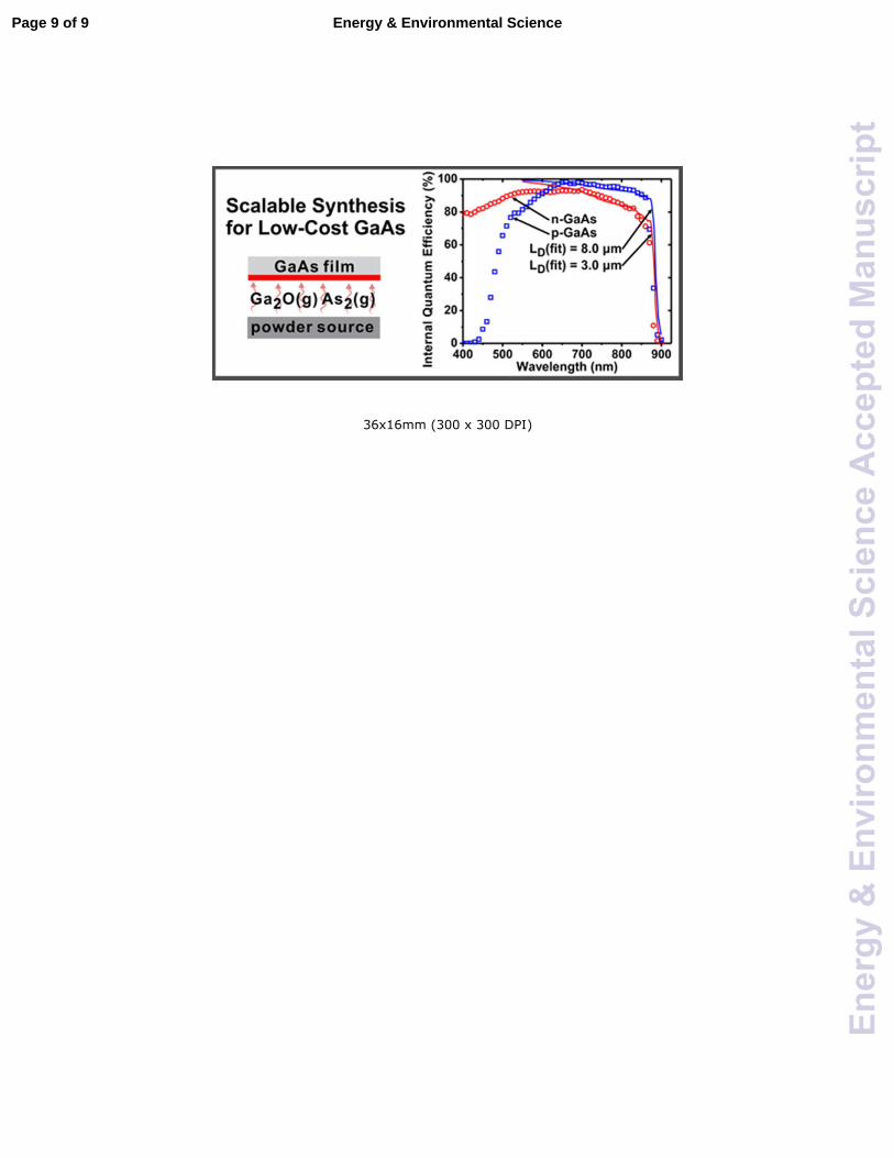
Conclusions
Epitaxial films of GaAs possessing a wide range of ND and NA were deposited via H2O-mediated CSVT with growth rate > 0.3 µm min-1 at ambient pressure from powdered GaAs precursors. ND and NA were measured and confirmed using complementary analyses which gave equivalent results (impedance spectroscopy, Hall Effect measurements, and TOF-SIMS). This is an important step toward the fabrication of more complex device architectures such as p-n junctions. The room temperature mobilities of CSVT GaAs films were similar to those produced in the literature using MOCVD, despite the relatively high growth rates and use of H2O vapor as a transport agent. Due to the high α(λ) of GaAs,55 the LD (2-3 µm for n-GaAs and 5-8 µm for p-GaAs) was sufficient to yield
Jsc ≈ 20 mA cm-2 which is near the one-sun limit (22.5 mA cm-
2) for specular GaAs with no anti-reflective coating in acetonitrile. For this µ e and LD we estimate an electron lifetime of τe ~ 7 ns for the NA = 1-2×1017 cm-3 p-GaAs films. According to previously published simulations28 using this lifetime, ƞ ≈ 25% single-junction photovoltaics could be fabricated if other device-engineering challenges (such as how to create rectifying solid-state junctions and passivate the surfaces) can be solved. Initial efforts to produce GaAs p-n junction PV solar cells using CSVT have produced promising results with Voc > 0.9 V and Φint > 0.9, but they are beyond the scope of this study.59 In addition to the high capital cost associated with MOCVD production of GaAs, lattice-matched substrates are also expensive relative to Si wafers. Tandem architectures which utilize the larger indirect band-gap and smaller lattice constant (closer to Si) of GaAsxP1-x could yield ƞ > 35% devices on Si substrates if challenges associated with the thermal and lattice mismatch can be addressed.60 Growth techniques such as selective area epitaxy12 and the synthesis and use of engineered strain relaxation areas61 may be required for such efforts.
Acknowledgements
This work was supported by the Department of Energy (DOE) SunShot Initiative BRIDGE program (DE-EE0005957). AR acknowledges support from the Julie and Rocky Dixon Graduate Innovation Fellowship. AG acknowledges support from a NSF Graduate Research Fellowship (DGE-0829517). SB acknowledges support from Research Corporation for Science Advancement as a Cottrell Scholar. We acknowledge support from the user program at the Molecular Foundry, Lawrence Berkeley National Laboratory, with funding from the U.S. DOE Office of Science, Office of Basic Energy Sciences under Contract DE-AC02-05CH1123. The CAMCOR shared instrument facilities are supported by grants from the W.M Keck Foundation, the M.J. Murdock Charitable Trust, ONAMI, and NSF. The SUNRISE Photovoltaic Laboratory is supported by Oregon Built Environment and Sustainable Technologies. Assistance from Fuding Lin, Adam Smith, Stephen Golledge, Fred Stevie, Kris Johnson, Jeff Garmin, John Boosinger, Cliff Dax, Alex Negrete, Richard Cramer, Solomon Levinrad, Athavan Nadarajah, Lena Trotochaud, Matthew Kast, Sangeun Chun, Michaela Burke, T.J. Mills, Adam Batchellor and David Senkovich is acknowledged.
Notes and References
1. O. D. Miller, E. Yablonovitch and S. R. Kurtz, IEEE J. Photovolt.,
2012, 2, 303-311.
2. W. Xufeng, M. R. Khan, J. L. Gray, M. A. Alam and M. S.
Lundstrom, IEEE J. Photovolt., 2013, 3, 737-744.
3. L. S. Mattos, S. R. Scully, M. Syfu, E. Olson, Y. Linlin, C. Ling, B.
M. Kayes and H. Gang, Proc. 38th IEEE Photovolt. Spec. Conf.,
2012, 3187-3190.
Page 7 of 9 Energy & Environmental Science
Ene
rgy
&E
nvir
onm
enta
lSci
ence
Acc
epte
dM
anus
crip
t

ARTICLE Journal Name
8 | J. Name., 2012, 00, 1-3 This journal is © The Royal Society of Chemistry 2012
4. M. A. Green, K. Emery, Y. Hishikawa, W. Warta and E. D. Dunlop,
Prog. Photovolt. Res. Appl., 2014, 22, 1-9.
5. E. Yablonovitch, O. D. Miller and S. R. Kurtz, Proc. 38th IEEE
Photovolt. Spec. Conf., 2012, 1556-1559.
6. M. Bosi and C. Pelosi, Prog. Photovolt. Res. Appl., 2007, 15, 51-68.
7. G. Perrier, R. Philippe and J. P. Dodelet, J. Mater. Res., 1988, 3,
1031-1042.
8. F. H. Nicoll, J. Electrochem. Soc., 1963, 110, 1165-1167.
9. E. Sirtl, J. Phys. Chem. Solids, 1963, 24, 1285-1289.
10. P. Robinson, RCA Rev, 1963, 24, 574-584.
11. M. Hammadi, J. C. Bourgoin and H. Samic, J. Mater. Sci.-Mater.
Electron., 1999, 10, 399-402.
12. M. G. Mauk, B. W. Feyock and J. E. Cotter, J. Cryst. Growth, 2001,
225, 528-533.
13. M. G. Mauk, A. N. Tata and B. W. Feyock, J. Cryst. Growth, 2001,
225, 359-365.
14. S. R. Kurtz and R. McConnell, AIP Conf. Proc., 1997, 404, 191-205.
15. R. Venkatasubramanian, B. O'Quinn and E. Siivola, AIP Conf. Proc.,
1997, 394, 259-270.
16. S. M. Vernon, S. P. Tobin, V. E. Haven, L. M. Geoffroy and M. M.
Sanfacon, Proc. 22nd IEEE Photovolt. Spec. Conf., 1991, 353-357
vol.351.
17. M. G. Mauk, J. R. Balliet and B. W. Feyock, J. Cryst. Growth, 2003,
250, 50-56.
18. M. G. Astles, Liquid-Phase Epitaxial Growth of III—V Compound
Semiconductor Materials and their Device Applications, Wiley-VCH
Verlag GmbH, 1990.
19. M. G. Mauk, B. W. Feyock, R. B. Hall, K. D. Cavanaugh and J. E.
Cotter, Proc. 26th IEEE Photovolt. Spec. Conf., 1997, 511-514.
20. F. Silva-Andrade, A. Ilinskii, F. Chavez, T. Prutskij, F. Tenorio, Y.
Bravo-Garcia and R. Pena-Sierra, Mod. Phys. Lett. B, 2001, 15, 752-
755.
21. P. A. Hoss, L. Murray and J. Rivera, J. Electrochem. Soc., 1968, 115,
553-556.
22. A. J. Ritenour and S. W. Boettcher, Proc. 38th IEEE Photovolt. Spec.
Conf., 2012, 913-917.
23. A. J. Ritenour, R. C. Cramer, S. Levinrad and S. W. Boettcher, ACS
Appl. Mater. Interfaces, 2012, 4, 69-73.
24. C. M. Gronet and N. S. Lewis, Appl. Phys. Lett., 1983, 43, 115-117.
25. R. Purohit, J. Mater. Sci., 1968, 3, 330-332.
26. W. Walukiewicz, L. Lagowski, L. Jastrzebski, M. Lichtensteiger and
H. C. Gatos, J. Appl. Phys., 1979, 50, 899-908.
27. M. Sotoodeh, A. Khalid and A. Rezazadeh, J. Appl. Phys., 2000, 87,
2890-2900.
28. J. W. Boucher, A. J. Ritenour and S. W. Boettcher, Proc. SPIE, 2013,
87250Z.
29. H. J. Scheel and P. Capper, eds., Crystal Growth Technology, Wiley-
VCH, 2008.
30. V. Rideout, Solid-State Electron., 1975, 18, 541-550.
31. L. G. Casagrande, A. Juang and N. S. Lewis, J. Phys. Chem. B, 2000,
104, 5436-5447.
32. F. R. F. Fan and A. J. Bard, J. Am. Chem. Soc., 1980, 102, 3677-
3683.
33. P. A. Kohl and A. J. Bard, J. Electrochem. Soc., 1979, 126, 59-67.
34. A. J. Ritenour, S. Levinrad, C. Bradley, R. C. Cramer and S. W.
Boettcher, ACS Nano, 2013.
35. K. E. Pomykal, A. M. Fajardo and N. S. Lewis, J. Phys.
Chem., 1995, 99, 8302-8310.
36. K. Gelderman, L. Lee and S. Donne, J. Chem. Educ., 2007, 84, 685.
37. S. M. Sze, Physics of Semiconductor Devices, John Wiley & Sons,
New York, 1981.
38. L. Van der Pauw, Philips Technical Review, 1958, 20, 220-224.
39. R. G. Wilson, F. A. Stevie and C. W. Magee, Secondary ion mass
spectrometry: a practical handbook for depth profiling and bulk
impurity analysis, Wiley New York, 1989.
40. B. Akamatsu, J. Henoc and P. Henoc, J. Appl. Phys., 1981, 52,
7245-7250.
41. B. J. Skromme, C. J. Sandroff, E. Yablonovitch and T. Gmitter,
Appl. Phys. Lett., 1987, 51, 2022-2024.
42. J. Bourgoin, D. Stievenard, D. Deresmes and J. Mimila Arroyo, J.
Appl. Phys., 1991, 69, 284-290.
43. C. Le Bel, D. Cossement, J. P. Dodelet, R. Leonelli, Y. DePuydt and
P. Bertrand, J. Appl. Phys., 1993, 73, 1288-1296.
44. E. Koskiahde, D. Cossement, R. Paynter, J. P. Dodelet, A. Jean and
B. A. Lombos, Can. J. Phys., 1989, 67, 251-258.
45. G. Gottlieb, J. Electrochem. Soc., 1965, 112, 192-196.
46. D. Cossement, J. P. Dodelet, T. Bretagnon, A. Jean and B. A.
Lombos, J. Electrochem. Soc., 1991, 138, 830-834.
47. L. G. Casagrande, B. J. Tufts and N. S. Lewis, J. Phys. Chem., 1991,
95, 1373-1380.
48. D. L. Rode and S. Knight, Physical Review B, 1971, 3, 2534-2541.
49. E. F. Schubert, Doping in III-V semiconductors, Cambridge Univ
Press, 1993.
50. G. K. Schweitzer and L. L. Pesterfield, The Aqueous Chemistry of
the Elements, Oxfort University Press, 2010.
51. W. W. Gӓrtner, Phys. Rev., 1959, 116, 84.
52. B. J. Tufts, I. L. Abrahams, L. G. Casagrande and N. S. Lewis, J.
Phys. Chem., 1989, 93, 3260-3269.
53. C. Xiang, G. M. Kimball, R. L. Grimm, B. S. Brunschwig, H. A.
Atwater and N. S. Lewis, Energ. Environ. Sci., 2011, 4, 1311-1318.
54. S. Adachi, Physical Properties of III-V Semiconductor Compounds,
John Wiley & Sons, First edn., 1992.
55. E. D. Palik, ed., Handbook of Optical Constants of Solids, Academic
Press, Inc., 1985.
56. S. R. Lunt, G. N. Ryba, P. G. Santangelo and N. S. Lewis, J. Appl.
Phys., 1991, 70, 7449-7467.
57. M. R. Brozel and G. Stillman, Properties of gallium arsenide, IET,
1996.
58. E. Fahrenkrug, J. Gu and S. Maldonado, J. Am. Chem. Soc., 2012,
135, 330-339.
59. J. W. Boucher, A. J. Ritenour, A. L. Greenaway, S. Aloni and S. W.
Boettcher, Proc. 40th IEEE Photovolt. Spec. Conf., 2014.
60. J. Faucher, A. Gerger, S. Tomasulo, C. Ebert, A. Lochtefeld, A.
Barnett and M. Lee, Appl. Phys. Lett., 2013, 103, 191901.
61. K. J. Schmieder, A. Gerger, M. Diaz, Z. Pulwin, C. Ebert, A.
Lochtefeld, R. Opila and A. Barnett, Proc. 38th IEEE Photovolt.
Spec. Conf., 2012, 968-973.
Page 8 of 9Energy & Environmental Science
Ene
rgy
&E
nvir
onm
enta
lSci
ence
Acc
epte
dM
anus
crip
t
36x16mm (300 x 300 DPI)
Page 9 of 9 Energy & Environmental Science
Ene
rgy
&E
nvir
onm
enta
lSci
ence
Acc
epte
dM
anus
crip
t