Figure II-2.2: Typical Steel Reinforced Elastomeric Bearing ...
Upload
independentCategory
view
0download
0
Purdue UniversityPurdue e-Pubs
Birck and NCN Publications Birck Nanotechnology Center
8-2012
A Batch-Fabricated Single-Layer ElastomericActuator With Corrugated SurfaceTeimour MalekiPurdue University, Birck Nanotechnology Center, [email protected]
Girish ChitnisPurdue University, Birck Nanotechnology Center, [email protected]
Albert KimPurdue University, Birck Nanotechnology Center, [email protected]
Babak ZiaiePurdue University, Birck Nanotechnology Center, [email protected]
Follow this and additional works at: http://docs.lib.purdue.edu/nanopubPart of the Nanoscience and Nanotechnology Commons
This document has been made available through Purdue e-Pubs, a service of the Purdue University Libraries. Please contact [email protected] foradditional information.
Maleki, Teimour; Chitnis, Girish; Kim, Albert; and Ziaie, Babak, "A Batch-Fabricated Single-Layer Elastomeric Actuator WithCorrugated Surface" (2012). Birck and NCN Publications. Paper 880.http://docs.lib.purdue.edu/nanopub/880
JOURNAL OF MICROELECTROMECHANICAL SYSTEMS, VOL. 21, NO. 4, AUGUST 2012 859
A Batch-Fabricated Single-Layer ElastomericActuator With Corrugated Surface
Teimour Maleki, Member, IEEE, Girish Chitnis, Albert Kim, and Babak Ziaie, Senior Member, IEEE
Abstract—In this paper, we report on the first laser-micromachined batch-fabricated single-layer elastomeric actuatorwith a corrugated surface profile. The structural material ofthe cantilever actuator is a single [polydimethylsiloxane (PDMS)]layer, and electrodes are soft lithographically patterned conductivecarbon grease. The asymmetric corrugated surface provides abending moment in a single PDMS layer without the need fora second inactive layer. An actuator which is 5 mm long, 1 mmwide, and 80 µm thick can generate up to 2-mm out-of-planedisplacement with zero applied force and 15 µN at zero de-flection while consuming 20 µW of static power when actuatedwith 500 V. [2011-0159]
Index Terms—Carbon grease, elastomeric actuators, elec-trostrictive polymers, laser micromachining, polydimethylsiloxane(PDMS).
I. INTRODUCTION
LOW-COST lightweight out-of-plane actuators are indis-pensable elements in a variety of robotics and biomedical
applications [1]–[4]. Electrostatic, magnetic, thermal, pneu-matic, piezoelectric, and several other actuation mechanisms,each with their unique advantages and disadvantages, havebeen used to implement such actuators [5]–[14]. Dielectricelastomer (DE) actuators are a new emerging class of electro-mechanical transducers with exceptional properties such aslarge strains, fast response, high efficiency/performance, lowcost, high fracture toughness, and inherent vibration damping[15]–[18]. These properties enable DE actuators to be a poten-tial candidate in large range of applications including artificialmuscle, microelectromechanical systems (MEMS), smart skin,and haptic displays [19]–[21]. One drawback of DE actuatorsis their high actuation voltages (in the kilovolt range). Severalgroups have attempted to address this issue (i.e., reducing theactuation voltage or increasing the strain for a given voltage)by various means such as modification of material properties,engineering new materials, improving electrode geometry, andmechanical contraptions such as film prestretching [22]–[27].Additional difficulty concerning DE actuators is their nonbatch-
Manuscript received May 22, 2011; revised February 8, 2012; acceptedMarch 14, 2012. Date of publication April 26, 2012; date of current versionJuly 27, 2012. Subject Editor F. Ayazi.
T. Maleki and A. Kim are with the Birck Nanotechnology Center, PurdueUniversity, West Lafayette, IN 47907 USA (e-mail: [email protected];[email protected]).
G. Chitnis is with Purdue University, West Lafayette, IN 47907 USA (e-mail:[email protected]).
B. Ziaie is with the School of Electrical and Computer Engineering, PurdueUniversity, West Lafayette, IN 47907 USA (e-mail: [email protected]).
Color versions of one or more of the figures in this paper are available onlineat http://ieeexplore.ieee.org.
Digital Object Identifier 10.1109/JMEMS.2012.2192909
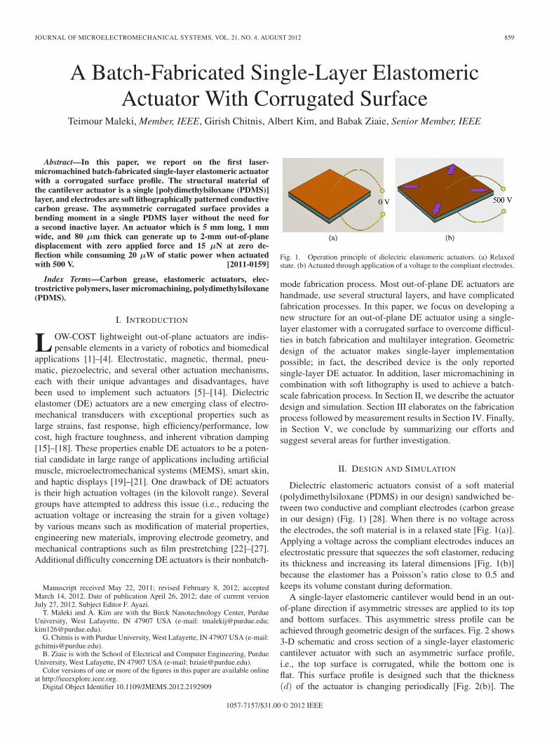
Fig. 1. Operation principle of dielectric elastomeric actuators. (a) Relaxedstate. (b) Actuated through application of a voltage to the compliant electrodes.
mode fabrication process. Most out-of-plane DE actuators arehandmade, use several structural layers, and have complicatedfabrication processes. In this paper, we focus on developing anew structure for an out-of-plane DE actuator using a single-layer elastomer with a corrugated surface to overcome difficul-ties in batch fabrication and multilayer integration. Geometricdesign of the actuator makes single-layer implementationpossible; in fact, the described device is the only reportedsingle-layer DE actuator. In addition, laser micromachining incombination with soft lithography is used to achieve a batch-scale fabrication process. In Section II, we describe the actuatordesign and simulation. Section III elaborates on the fabricationprocess followed by measurement results in Section IV. Finally,in Section V, we conclude by summarizing our efforts andsuggest several areas for further investigation.
II. DESIGN AND SIMULATION
Dielectric elastomeric actuators consist of a soft material(polydimethylsiloxane (PDMS) in our design) sandwiched be-tween two conductive and compliant electrodes (carbon greasein our design) (Fig. 1) [28]. When there is no voltage acrossthe electrodes, the soft material is in a relaxed state [Fig. 1(a)].Applying a voltage across the compliant electrodes induces anelectrostatic pressure that squeezes the soft elastomer, reducingits thickness and increasing its lateral dimensions [Fig. 1(b)]because the elastomer has a Poisson’s ratio close to 0.5 andkeeps its volume constant during deformation.
A single-layer elastomeric cantilever would bend in an out-of-plane direction if asymmetric stresses are applied to its topand bottom surfaces. This asymmetric stress profile can beachieved through geometric design of the surfaces. Fig. 2 shows3-D schematic and cross section of a single-layer elastomericcantilever actuator with such an asymmetric surface profile,i.e., the top surface is corrugated, while the bottom one isflat. This surface profile is designed such that the thickness(d) of the actuator is changing periodically [Fig. 2(b)]. The
1057-7157/$31.00 © 2012 IEEE
860 JOURNAL OF MICROELECTROMECHANICAL SYSTEMS, VOL. 21, NO. 4, AUGUST 2012
Fig. 2. (a) Three-dimensional schematic and (b) cross-sectional view of asingle-layer elastomeric actuator with an asymmetric surface profile.
structure thickness can be thought of as a superposition of twocomponents, a constant term (t) with a square wave (magnitudeA and frequency ω) superposition representing the corrugation.When a constant voltage is applied across top and bottomelectrodes, the resulting transverse stress in the elastomer canbe approximated as
σ = −12εε0
V 2
(t ± A)2(1)
where ε is the elastomer dielectric constant, εo is the airpermeability, and V is the applied voltage. The asymmetricsurface profile induces a nonuniform transverse compressionand longitudinal expansion, resulting in a bending moment inthe cantilever.
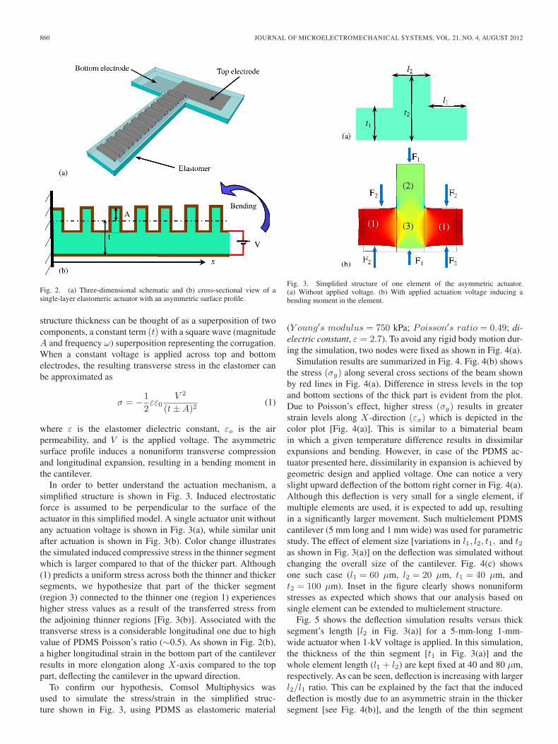
In order to better understand the actuation mechanism, asimplified structure is shown in Fig. 3. Induced electrostaticforce is assumed to be perpendicular to the surface of theactuator in this simplified model. A single actuator unit withoutany actuation voltage is shown in Fig. 3(a), while similar unitafter actuation is shown in Fig. 3(b). Color change illustratesthe simulated induced compressive stress in the thinner segmentwhich is larger compared to that of the thicker part. Although(1) predicts a uniform stress across both the thinner and thickersegments, we hypothesize that part of the thicker segment(region 3) connected to the thinner one (region 1) experienceshigher stress values as a result of the transferred stress fromthe adjoining thinner regions [Fig. 3(b)]. Associated with thetransverse stress is a considerable longitudinal one due to highvalue of PDMS Poisson’s ratio (∼0.5). As shown in Fig. 2(b),a higher longitudinal strain in the bottom part of the cantileverresults in more elongation along X-axis compared to the toppart, deflecting the cantilever in the upward direction.
To confirm our hypothesis, Comsol Multiphysics wasused to simulate the stress/strain in the simplified struc-ture shown in Fig. 3, using PDMS as elastomeric material
Fig. 3. Simplified structure of one element of the asymmetric actuator.(a) Without applied voltage. (b) With applied actuation voltage inducing abending moment in the element.
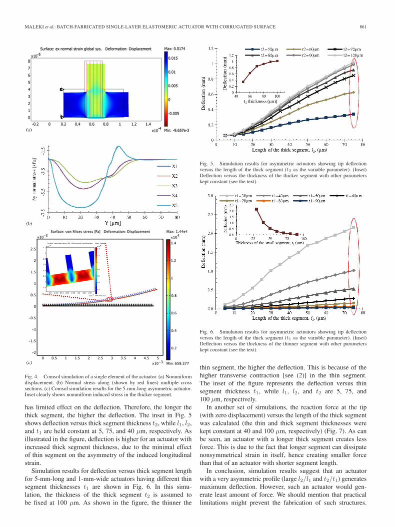
(Y oung′s modulus = 750 kPa; Poisson′s ratio = 0.49; di-electric constant, ε = 2.7). To avoid any rigid body motion dur-ing the simulation, two nodes were fixed as shown in Fig. 4(a).
Simulation results are summarized in Fig. 4. Fig. 4(b) showsthe stress (σy) along several cross sections of the beam shownby red lines in Fig. 4(a). Difference in stress levels in the topand bottom sections of the thick part is evident from the plot.Due to Poisson’s effect, higher stress (σy) results in greaterstrain levels along X-direction (εx) which is depicted in thecolor plot [Fig. 4(a)]. This is similar to a bimaterial beamin which a given temperature difference results in dissimilarexpansions and bending. However, in case of the PDMS ac-tuator presented here, dissimilarity in expansion is achieved bygeometric design and applied voltage. One can notice a veryslight upward deflection of the bottom right corner in Fig. 4(a).Although this deflection is very small for a single element, ifmultiple elements are used, it is expected to add up, resultingin a significantly larger movement. Such multielement PDMScantilever (5 mm long and 1 mm wide) was used for parametricstudy. The effect of element size [variations in l1, l2, t1, and t2as shown in Fig. 3(a)] on the deflection was simulated withoutchanging the overall size of the cantilever. Fig. 4(c) showsone such case (l1 = 60 µm, l2 = 20 µm, t1 = 40 µm, andt2 = 100 µm). Inset in the figure clearly shows nonuniformstresses as expected which shows that our analysis based onsingle element can be extended to multielement structure.
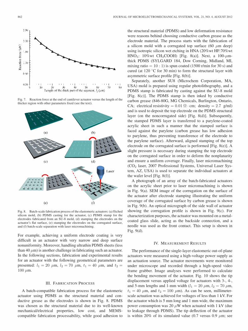
Fig. 5 shows the deflection simulation results versus thicksegment’s length [l2 in Fig. 3(a)] for a 5-mm-long 1-mm-wide actuator when 1-kV voltage is applied. In this simulation,the thickness of the thin segment [t1 in Fig. 3(a)] and thewhole element length (l1 + l2) are kept fixed at 40 and 80 µm,respectively. As can be seen, deflection is increasing with largerl2/l1 ratio. This can be explained by the fact that the induceddeflection is mostly due to an asymmetric strain in the thickersegment [see Fig. 4(b)], and the length of the thin segment
MALEKI et al.: BATCH-FABRICATED SINGLE-LAYER ELASTOMERIC ACTUATOR WITH CORRUGATED SURFACE 861
Fig. 4. Comsol simulation of a single element of the actuator. (a) Nonuniformdisplacement. (b) Normal stress along (shown by red lines) multiple crosssections. (c) Comsol simulation results for the 5-mm-long asymmetric actuator.Inset clearly shows nonuniform induced stress in the thicker segment.
has limited effect on the deflection. Therefore, the longer thethick segment, the higher the deflection. The inset in Fig. 5shows deflection versus thick segment thickness t2, while l1, l2,and t1 are held constant at 5, 75, and 40 µm, respectively. Asillustrated in the figure, deflection is higher for an actuator withincreased thick segment thickness, due to the minimal effectof thin segment on the asymmetry of the induced longitudinalstrain.
Simulation results for deflection versus thick segment lengthfor 5-mm-long and 1-mm-wide actuators having different thinsegment thicknesses t1 are shown in Fig. 6. In this simu-lation, the thickness of the thick segment t2 is assumed tobe fixed at 100 µm. As shown in the figure, the thinner the
Fig. 5. Simulation results for asymmetric actuators showing tip deflectionversus the length of the thick segment (t2 as the variable parameter). (Inset)Deflection versus the thickness of the thicker segment with other parameterskept constant (see the text).
Fig. 6. Simulation results for asymmetric actuators showing tip deflectionversus the length of the thick segment (t1 as the variable parameter). (Inset)Deflection versus the thickness of the thinner segment with other parameterskept constant (see the text).
thin segment, the higher the deflection. This is because of thehigher transverse contraction [see (2)] in the thin segment.The inset of the figure represents the deflection versus thinsegment thickness t1, while l1, l2, and t2 are 5, 75, and100 µm, respectively.
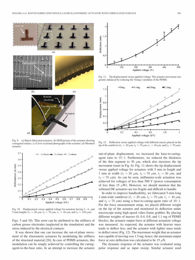
In another set of simulations, the reaction force at the tip(with zero displacement) versus the length of the thick segmentwas calculated (the thin and thick segment thicknesses werekept constant at 40 and 100 µm, respectively) (Fig. 7). As canbe seen, an actuator with a longer thick segment creates lessforce. This is due to the fact that longer segment can dissipatenonsymmetrical strain in itself, hence creating smaller forcethan that of an actuator with shorter segment length.
In conclusion, simulation results suggest that an actuatorwith a very asymmetric profile (large l2/l1 and t2/t1) generatesmaximum deflection. However, such an actuator would gen-erate least amount of force. We should mention that practicallimitations might prevent the fabrication of such structures.
862 JOURNAL OF MICROELECTROMECHANICAL SYSTEMS, VOL. 21, NO. 4, AUGUST 2012
Fig. 7. Reaction force at the end of cantilever actuator versus the length of thethicker region with other parameters fixed (see the text).
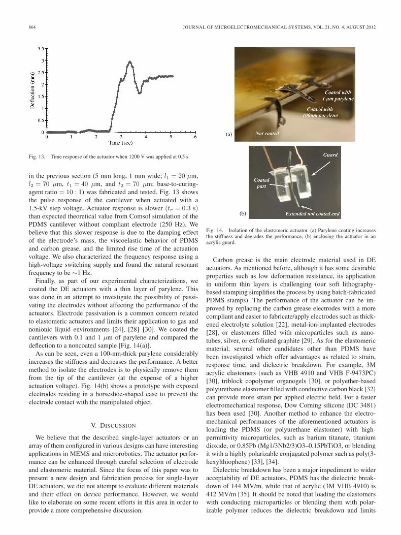
Fig. 8. Batch-scale fabrication process of the elastomeric actuators: (a) Etchedsilicon mold, (b) PDMS casting for the actuator, (c) PDMS stamp for theelectrodes fabricated from an SU-8 mold, (d) stamping the electrodes on theactuator’s flat surface, (e) stamping the electrodes on the corrugated surface,and (f) batch-scale separation with laser micromachining.
For example, achieving a uniform electrode coating is verydifficult in an actuator with very narrow and deep surfacenonuniformity. Moreover, handling ultrathin PDMS sheets (lessthan 40 µm) is another challenge in fabricating such an actuator.In the following sections, fabrication and experimental resultsfor an actuator with the following geometrical parameters arepresented: l1 = 20 µm, l2 = 70 µm, t1 = 40 µm, and t2 =100 µm.
III. FABRICATION PROCESS
A batch-compatible fabrication process for the elastomericactuator using PDMS as the structural material and con-ductive grease as the electrodes is shown in Fig. 8. PDMSwas chosen as the structural material due to its well-knownmechanical/electrical properties, low cost, and MEMS-compatible fabrication processability, while good adhesion to
the structural material (PDMS) and low deformation resistancewere reasons behind choosing conductive carbon grease as theelectrode material. The process starts with the fabrication ofa silicon mold with a corrugated top surface (60 µm deep)using isotropic silicon wet etching in HNA (20%wt HF:70%wtHNO3: 10%wt CH3COOH) [Fig. 8(a)]. Next, a 100-µm-thick PDMS (SYLGARD 184, Dow Corning, Midland, MI,mixing ratio = 10 : 1) is spun coated (1500 r/min for 30 s) andcured (at 120 C for 30 min) to form the structural layer withasymmetric surface profile [Fig. 8(b)].
Separately, another SU8 (Microchem Corporation, MA,USA) mold is prepared using regular photolithography, and aPDMS stamp is fabricated by casting against the SU-8 mold[Fig. 8(c)]. The PDMS stamp is then inked by conductivecarbon grease (846-80G, MG Chemicals, Burlington, Ontario,CA; electrical resistivity = 0.01 Ω · cm; density = 2.7 g/ml)and is used to deposit the top electrode on the PDMS structurallayer (on the noncorrugated side) [Fig. 8(d)]. Subsequently,the stamped PDMS layer is transferred to a parylene-coatedacrylic sheet in such a manner that the stamped surface isfaced against the parylene (carbon grease has low adhesionto parylene, thus preventing transference of the electrode tothe parylene surface). Afterward, aligned stamping of the topelectrode on the corrugated surface is performed [Fig. 8(e)]. Aslight pressure is necessary during stamping the top electrodeon the corrugated surface in order to deform the nonplanarityand ensure a uniform coverage. Finally, laser micromachining(CO2 laser, 2007 Professional Systems, Universal Laser Sys-tem, AZ, USA) is used to separate the individual actuators atthe wafer level [Fig. 8(f)].
A photograph of an array of the batch-fabricated actuatorson the acrylic sheet prior to laser micromachining is shownin Fig. 9(a). SEM image of the corrugation on the surface ofthe actuator after electrode stamping illustrating the uniformcoverage of the corrugated surface by carbon grease is shownin Fig. 9(b). An optical micrograph of the side wall of actuatorshowing the corrugation profile is shown in Fig. 9(c). Forcharacterization purposes, the actuator was mounted on a metal-coated glass slide, acting as the backside connection, and aneedle was used as the front contact. This setup is shown inFig. 9(d).
IV. MEASUREMENT RESULTS
The performance of the single-layer elastomeric out-of-planeactuators were measured using a high-voltage power supply asan actuation source. The actuator movements were monitoredunder microscope and recorded through a high-speed videoframe grabber. Image analyses were performed to calculatethe bending movement of the actuator. Fig. 10 shows the tipdisplacement versus applied voltage for actuators with 3-, 4-,and 5-mm lengths and 1-mm width (l1 = 20 µm, l2 = 70 µm,t1 = 40 µm, and t2 = 100 µm). As can be seen, millimeter-scale actuation was achieved for voltages of less than 1 kV. Forthe actuator which is 5 mm long and 1 mm wide, the maximumpower consumption was 20 µW when actuated with 1 kV (dueto leakage through PDMS). The tip deflection of the actuatoris within 20% of its simulated value (0.7 versus 0.9 µm; see
MALEKI et al.: BATCH-FABRICATED SINGLE-LAYER ELASTOMERIC ACTUATOR WITH CORRUGATED SURFACE 863
Fig. 9. (a) Batch-fabricated actuators. (b) SEM picture of the actuator showingcorrugated surface. (c) Cross-sectional photograph of the actuator. (d) Mountedactuator.
Fig. 10. Displacement versus applied voltage for actuators having 3-, 4-, and5-mm lengths (l1 = 20 µm, l2 = 70 µm, t1 = 40 µm, and t2 = 100 µm).
Figs. 5 and 10). This error can be attributed to the stiffness ofcarbon grease electrodes (neglected in the simulation) and thestress induced by the electrical contacts.
It was shown that one can increase the out-of-plane move-ment of the elastomeric actuators by modulating the stiffnessof the structural material [26]. In case of PDMS actuators, thismodulation can be simply achieved by controlling the curing-agent-to-the-base ratio. In an attempt to increase the actuator
Fig. 11. Tip displacement versus applied voltage. The actuator movement wasgreatly enhanced by reducing the Young’s modulus of the PDMS.
Fig. 12. Deflection versus applied voltage with different masses placed on thetip of the cantilever (l1 = 20 µm, l2 = 70 µm, t1 = 40 µm, and t2 = 70 µm).
out-of-plane displacement, we increased the base-to-curing-agent ratio to 15 : 1. Furthermore, we reduced the thicknessof the thin segment to 30 µm, which also increases the tipmovement (inset in Fig. 6). Fig. 11 shows the tip displacementversus applied voltage for actuators with 5 mm in length and1 mm in width (l1 = 20 µm, l2 = 70 µm, t1 = 30 µm, andt2 = 70 µm). As can be seen, millimeter-scale actuation wasachieved for voltages of less than 500 V (power consumptionof less than 15 µW). However, we should mention that thesoftened DE actuators are too fragile and difficult to handle.
In order to improve handleability, we fabricated 5-mm-long1-mm-wide cantilever (l1 = 20 µm, l2 = 70 µm, t1 = 40 µm,and t2 = 70 µm) using a base-to-curing-agent ratio of 10 : 1.For the force measurement setup, we placed different weighton the tip of the actuator and monitored its deflection undermicroscope using high-speed video frame grabber. By placingdifferent weights of masses (0, 0.4, 0.8, and 1.1 mg of PDMSblocks), the actuator output force at different actuation voltagewas measured. As expected, the actuator with heavier masstends to deflect less, and the actuator with lighter mass tendsto deflect more (Fig. 12). The maximum weight that an actuatorwas capable of moving was 1.5 mg; hence, the maximum outputforce at zero deflection was calculated to be 15 µN.
The dynamic response of the actuator was evaluated usingpulse response and ac input sweep. Similar actuator used
864 JOURNAL OF MICROELECTROMECHANICAL SYSTEMS, VOL. 21, NO. 4, AUGUST 2012
Fig. 13. Time response of the actuator when 1200 V was applied at 0.5 s.
in the previous section (5 mm long, 1 mm wide; l1 = 20 µm,l2 = 70 µm, t1 = 40 µm, and t2 = 70 µm; base-to-curing-agent ratio = 10 : 1) was fabricated and tested. Fig. 13 showsthe pulse response of the cantilever when actuated with a1.5-kV step voltage. Actuator response is slower (tr = 0.3 s)than expected theoretical value from Comsol simulation of thePDMS cantilever without compliant electrode (250 Hz). Webelieve that this slower response is due to the damping effectof the electrode’s mass, the viscoelastic behavior of PDMSand carbon grease, and the limited rise time of the actuationvoltage. We also characterized the frequency response using ahigh-voltage switching supply and found the natural resonantfrequency to be ∼1 Hz.
Finally, as part of our experimental characterizations, wecoated the DE actuators with a thin layer of parylene. Thiswas done in an attempt to investigate the possibility of passi-vating the electrodes without affecting the performance of theactuators. Electrode passivation is a common concern relatedto elastomeric actuators and limits their application to gas andnonionic liquid environments [24], [28]–[30]. We coated thecantilevers with 0.1 and 1 µm of parylene and compared thedeflection to a noncoated sample [Fig. 14(a)].
As can be seen, even a 100-nm-thick parylene considerablyincreases the stiffness and decreases the performance. A bettermethod to isolate the electrodes is to physically remove themfrom the tip of the cantilever (at the expense of a higheractuation voltage). Fig. 14(b) shows a prototype with exposedelectrodes residing in a horseshoe-shaped case to prevent theelectrode contact with the manipulated object.
V. DISCUSSION
We believe that the described single-layer actuators or anarray of them configured in various designs can have interestingapplications in MEMS and microrobotics. The actuator perfor-mance can be enhanced through careful selection of electrodeand elastomeric material. Since the focus of this paper was topresent a new design and fabrication process for single-layerDE actuators, we did not attempt to evaluate different materialsand their effect on device performance. However, we wouldlike to elaborate on some recent efforts in this area in order toprovide a more comprehensive discussion.
Fig. 14. Isolation of the elastomeric actuator. (a) Parylene coating increasesthe stiffness and degrades the performance, (b) enclosing the actuator in anacrylic guard.
Carbon grease is the main electrode material used in DEactuators. As mentioned before, although it has some desirableproperties such as low deformation resistance, its applicationin uniform thin layers is challenging (our soft lithography-based stamping simplifies the process by using batch-fabricatedPDMS stamps). The performance of the actuator can be im-proved by replacing the carbon grease electrodes with a morecompliant and easier to fabricate/apply electrodes such as thick-ened electrolyte solution [22], metal-ion-implanted electrodes[28], or elastomers filled with microparticles such as nano-tubes, silver, or exfoliated graphite [29]. As for the elastomericmaterial, several other candidates other than PDMS havebeen investigated which offer advantages as related to strain,response time, and dielectric breakdown. For example, 3Macrylic elastomers (such as VHB 4910 and VHB F-9473PC)[30], triblock copolymer organogels [30], or polyether-basedpolyurethane elastomer filled with conductive carbon black [32]can provide more strain per applied electric field. For a fasterelectromechanical response, Dow Corning silicone (DC 3481)has been used [30]. Another method to enhance the electro-mechanical performances of the aforementioned actuators isloading the PDMS (or polyurethane elastomer) with high-permittivity microparticles, such as barium titanate, titaniumdioxide, or 0.85Pb (Mg1/3Nb2/3)O3–0.15PbTiO3, or blendingit with a highly polarizable conjugated polymer such as poly(3-hexylthiophene) [33], [34].
Dielectric breakdown has been a major impediment to wideracceptability of DE actuators. PDMS has the dielectric break-down of 144 MV/m, while that of acrylic (3M VHB 4910) is412 MV/m [35]. It should be noted that loading the elastomerswith conducting microparticles or blending them with polar-izable polymer reduces the dielectric breakdown and limits
MALEKI et al.: BATCH-FABRICATED SINGLE-LAYER ELASTOMERIC ACTUATOR WITH CORRUGATED SURFACE 865
the maximum operating voltage [33], whereas nonconductingmicroparticles result in a higher dielectric breakdown [36].
VI. CONCLUSION
In conclusion, a batch fabrication process for a single-layerelastomeric actuator based on asymmetric surface profile hasbeen presented. Comsol simulations were performed showingthat a more nonuniform profile would generate a greater deflec-tion. Successful fabrication and characterization of three differ-ent sizes of actuators with geometry optimized for maximumout-of-plane deflection were presented. There was a reasonableagreement between the measurements and the Comsol simu-lation results (within 20%). Cantilever beams actuated withvoltages as low as 500 V could achieve millimeter-scale out-of-plane displacements. A 5-mm-long actuator was capable ofgenerating 15-µN force when actuated with 500 V and con-sumed less than 20 µw of power. Although a simple cantileverbeam was presented in this paper, similar concept can be ap-plied to several other geometrical designs such as membranes,double-clamped beams, and spiral structures. Applications ofthis technology can include micropumps, microvalves, andminiaturized manipulators.
ACKNOWLEDGMENT
The authors would like to thank the staff at the BirckNanotechnology Center, Purdue University, for their assis-tance in fabrication. The authors would also like to thankProf. C. Savran for his help with laser micromachining.
REFERENCES
[1] M. T. Azar, Microactuators: Electrical, Magnetic, Thermal, Optical, Me-chanical, Chemical and Smart Structures. New York: Springer-Verlag,1997.
[2] H. Janoch, Ed., Actuators: Basics and Applications. New York:Springer-Verlag, 2010.
[3] H. Janoch, Ed., Adaptronics and Smart Structures: Basics, Materials,Design, and Applications. NY: Springer-Verlag, 2010.
[4] R. D. Howe and Y. Matsuka, “Robotic for surgery,” Annu. Rev. Biomed.Eng., vol. 1, pp. 211–240, 1999.
[5] H. Kim, A. Ucok, and K. Najafi, “Large-deflection stacked multi-electrode electrostatic actuator,” in Proc. 11th Solid-State Sens., Actuator,Microsyst. Workshop, Hilton Head Island, SC, 2004, pp. 340–343.
[6] J. D. Grade, H. Jerman, and T. W. Kenny, “Design of large deflectionelectrostatic actuators,” J. Microelectromech. Syst., vol. 12, no. 3, pp. 335–343, Jun. 2003.
[7] C. Liu, T. Tsao, G. B. Lee, J. T. S. Leu, Y. W. Yi, Y. C. Tai, and C. M. Ho,“Out-of-plane magnetic actuators with electroplated permalloy for fluiddynamics control,” Sens. Actuators A, Phys., vol. 78, no. 2/3, pp. 190–197, Dec. 1999.
[8] Y. A. Pimpin, Y. Suzuki, and N. Kasagi, “Microelectrostrictive actu-ator with large out-of-plane deformation for flow-control application,”J. Microelectromech. Syst., vol. 16, no. 3, pp. 753–764, Jun. 2007.
[9] A. Michael, C. Y. Kwok, K. Yu, and M. R. Mackenzie, “A novel bistabletwo-way actuated out-of-plane electrothermal microbridge,” J. Micro-electromech. Syst., vol. 17, no. 1, pp. 58–69, Feb. 2008.
[10] D. Girbau, M. A. Llamas, J. Casals-Terré, X. Simó-Selvas, L. Pradell,and A. Lázaro, “A low-power-consumption out-of-plane electrother-mal actuator,” J. Microelectromech. Syst., vol. 16, no. 3, pp. 719–727,Jun. 2007.
[11] W. C. Chen, C. C. Chu, J. Hsieh, and W. Fang, “A reliable single-layerout-of-plane micromachined thermal actuator,” Sens. Actuators A, Phys.,vol. 103, no. 1/2, pp. 48–58, 2003.
[12] Y. Lu and C. J. Kim, “Micro-finger articulation by pneumatic paryleneballoons,” in Proc. 12th Int. Conf. Solid State Sens., Actuators Microsyst.,Boston, MA, 2003, pp. 276–279.
[13] J. Juuti, K. Kordás, R. Lonnakko, V. P. Moilanen, and S. Leppävuori, “Me-chanically amplified large displacement piezoelectric actuators,” Sens.Actuators A, Phys., vol. 120, no. 1, pp. 225–231, Apr. 2005.
[14] V. Monturet and B. Nogarede, “Optimal dimensioning of a piezoelec-tric bimorph actuator,” Eur. J. Appl. Phys., vol. 17, no. 2, pp. 107–118,Feb. 2002.
[15] F. Carpi, D. D. Rossi, R. Kornbluh, and R. E. Pelrine, Eds., DielectricElastomers as Electromechanical Transducers: Fundamentals, Materials,Devices, Models and Applications of an Emerging Electroactive PolymerTechnology. New York: Elsevier, 2008.
[16] A. O’Halloran, F. O’Malley, and P. McHugh, “A review on dielectricelastomer actuators, technology, applications, and challenges,” J. Appl.Phys., vol. 104, no. 7, pp. 071101-1–071101-10, Oct. 2008.
[17] J. S. Plante and S. Dubowsky, “On the properties of dielectric elastomeractuators and their design implications,” Smart Mater. Struct., vol. 16,no. 2, pp. s227–S236, Apr. 2007.
[18] R. Kornbluh, R. Pelrine, Q. Pei, R. Heydt, S. Stanford, S. Oh, andJ. Eckerle, “Electroelastomers: Applications of dielectric elastomer trans-ducers for actuation, generation and smart structures,” in Proc. SPIE, SanDiego, CA, 2002, pp. 254–270.
[19] F. Carpi, G. Frediani, A. Mannini, and D. D. Rossi, “Contractile and buck-ling actuators based on dielectric elastomers: Devices and applications,”Adv. Sci. Technol., vol. 61, pp. 186–191, 2008.
[20] R. H. Baughman, “Playing nature’s game with artificial muscles,” Sci-ence, vol. 308, no. 5718, pp. 63–65, Apr. 2005.
[21] R. Pe1rine, P. S. Larsen, R. Kornbluh, R. Heydt, G. Kofod, and Q. Pei,“Applications of dielectric elastomer actuators,” in Proc. SPIE, NewportBeach, CA, 2001, vol. 4329, pp. 335–349.
[22] F. Carpi, P. Chiarelli, A. Mazzoldi, and D. D. Rossi, “Electromechani-cal characterization of dielectric elastomer planar actuators: Comparativeevaluation of different electrode materials and different counter loads,”Sens. Actuators A, Phys., vol. 107, pp. 85–95, 2003.
[23] R. Kornbluh and R. Pelrine, “High-performance acrylic and siliconeelastomers,” in Dielectric Elastomers as Electromechanical Transduc-ers: Fundamentals, Materials, Devices, Models and Applications of anEmerging Electroactive Polymer Technology. New York: Elsevier, 2008,pp. 33–42.
[24] R. Pelrine, R. Kornbluh, Q. Pei, and J. Joseph, “High-speed electricallyactuated elastomers with strain greater than 100%,” Science, vol. 287,no. 5454, pp. 836–839, Feb. 2000.
[25] R. Pelrine, R. Kornbluh, and G. Kofod, “High-strain actuator materialsbased on dielectric elastomers,” Adv. Mater., vol. 12, no. 16, pp. 1223–1225, Aug. 2000.
[26] T. Maleki, G. Chitnis, and B. Ziaie, “A batch-fabricated laser-micromachined PDMS actuator with stamped carbon grease electrodes,”J. Micromech. Microeng., vol. 21, no. 2, p. 027002, Feb. 2011.
[27] R. Pelrine, R. Kornbluh, J. Joseph, R. Heydt, Q. Pei, and S. Chiba, “High-field deformation of elastomeric dielectrics for actuators,” Mater. Sci.Eng., C, vol. 11, no. 2, pp. 89–100, Nov. 2000.
[28] S. Rosset, M. Niklaus, P. Dubois, and H. R. Shea, “Mechanical char-acterization of a dielectric elastomer microactuator with ion-implantedelectrodes,” Sens. Actuators A, Phys., vol. 144, no. 1, pp. 185–193, 2008.
[29] M. Kujawski, J. D. Pearse, and E. Smela, “Elastomers filled with exfoli-ated graphite as compliant electrodes,” Carbon, vol. 48, no. 9, pp. 2409–2417, Aug. 2010.
[30] S. Michel, X. Q. Zhang, M. Wissler, C. Lowe, and G. Kovacs, “A com-parison between silicone and acrylic elastomers as dielectric materials inelectroactive polymer actuators,” Polym. Int., vol. 59, no. 3, pp. 391–399,Mar. 2010.
[31] R. Shankar, A. K. Krishnan, T. K. Ghosh, and R. J. Spontak, “Tri-block copolymer organogels as high-performance dielectric elastomers,”Macromolecules, vol. 41, no. 16, pp. 6100–6109, Aug. 2008.
[32] K. Wongtimnoi, B. Guiffard, A. Bogner-Van de Moortèle, L. Seveyrat,C. Gauthier, and J.-Y. Cavaillé, “Improvement of electrostrictive proper-ties of a polyether-based polyurethane elastomer filled with conductivecarbon black,” Composites Sci. Technol., vol. 71, no. 6, pp. 885–892,Apr. 2011.
[33] G. Gallone, F. Galantini, and F. Carpi, “Perspectives for new dielec-tric elastomers with improved electromechanical actuation performance:Composites versus blends,” Polym. Int., vol. 59, pp. 400–406, 2010.
[34] F. Carpi, G. Gallone, F. Galantini, and D. D. Rossi, “Silicone-poly(hexylthiophene) blends as elastomers with enhanced electromechanicaltransduction properties,” Adv. Funct. Mater., vol. 18, no. 2, pp. 235–241,Jan. 2008.
866 JOURNAL OF MICROELECTROMECHANICAL SYSTEMS, VOL. 21, NO. 4, AUGUST 2012
[35] P. Brochu and Q. Pei, “Advances in dielectric elastomers for actuators andartificial muscles,” Macromol. Rapid Commun., vol. 31, no. 1, pp. 10–36,Jan. 2010.
[36] G. Kofod, H. Stoyanov, M. Kollosche, S. Risse, H. Ragusch,D. N. McCarthy, R. Waché, D. Rychkov, and M. Dansachmüller, “Mole-cular level materials design for improvements of actuation propertiesof dielectric elastomer actuators,” in Proc. SPIE, 2011, vol. 7976,pp. 79760J-1–79760J-12.
Teimour Maleki (M’09) received the B.Sc. degreein biomedical engineering from Amirkabir Univer-sity of Technology, Tehran, Iran, in 2000, the M.Sc.degree in electrical engineering from the Universityof Tehran, Tehran, in 2003, and the Ph.D. degree inelectrical engineering from Purdue University, WestLafayette, IN, in 2010.
He is currently a Research Assistant Pro-fessor with the Birck Nanotechnology Center,Purdue University. His focus is on developingmicroelectromechanical-systems-enabled point-of-
care systems for healthcare and implantable microdevices.
Girish Chitnis received the B.S. degree in mechani-cal engineering from the Indian Institute of Technol-ogy Bombay, Mumbai, India, in 2007. In 2007, hejoined Purdue University, West Lafayette, IN, wherehe is currently working toward the Ph.D. degree inengineering.
His research interests are related to micro-electromechanical systems and their biomedicalapplications.
Albert Kim was born in Delaware in 1983. Hereceived the B.S. and M.S. degrees from PurdueUniversity, West Lafayette, IN, where he is cur-rently working toward the Ph.D. degree in electricalengineering.
He is currently a member of a research team,ZBML, that is developing biomedical devices atthe Birck Nanotechnology Center, Purdue Univer-sity. His interests include design and fabricationof implantable devices for energy scavenging fromacoustic waves and liquid-based microtransponders.
Babak Ziaie (A’95–M’00–SM’07) received thePh.D. degree in electrical engineering from the Uni-versity of Michigan, Ann Arbor, in 1994.
From 1995 to 1999, he was a Postdoctoral Fel-low and an Assistant Research Scientist with theCenter for Integrated Microsystems, University ofMichigan. He subsequently joined the Electrical andComputer Engineering Department, University ofMinnesota, Minneapolis, as an Assistant Professor(1999–2004). Since January 2005, he has been withthe School of Electrical and Computer Engineering,
Purdue University, West Lafayette, IN, where he is currently a Professor. Hisresearch interests are related to the biomedical applications of microelectro-mechanical systems and microsystems (bioMEMS).
Copyright © 2022 FDOKUMEN