Interfacial rheology of coextruded elastomeric and amorphous glass thermoplastic polyurethanes
Upload
independentCategory
view
4download
0
Purdue UniversityPurdue e-Pubs
ECE Faculty Publications Electrical and Computer Engineering
2009
A biaxial stretchable interconnect with liquid-alloy-covered joints on elastomeric substrateKim Hyun-Joong
T. Maleki
Wei Pinghung
B. Ziaie
This document has been made available through Purdue e-Pubs, a service of the Purdue University Libraries. Please contact [email protected] foradditional information.
Hyun-Joong, Kim; Maleki, T.; Pinghung, Wei; and Ziaie, B., "A biaxial stretchable interconnect with liquid-alloy-covered joints onelastomeric substrate" (2009). ECE Faculty Publications. Paper 11.http://docs.lib.purdue.edu/ecepubs/11

138 JOURNAL OF MICROELECTROMECHANICAL SYSTEMS, VOL. 18, NO. 1, FEBRUARY 2009
A Biaxial Stretchable Interconnect WithLiquid-Alloy-Covered Joints on
Elastomeric SubstrateHyun-Joong Kim, Teimour Maleki, Pinghung Wei, and Babak Ziaie, Senior Member, IEEE
Abstract—This paper reports a biaxial stretchable intercon-nect on an elastomeric substrate. To increase the stretchabilityof interconnects, a 2-D diamond-shaped geometry of gold on apolydimethylsiloxane substrate was adopted in which the poten-tially breakable points were covered with room temperature liquidalloy. Finite element model simulations were performed to iden-tify the most vulnerable points subjected to stress concentrationand optimize the design process. Simulations also indicated anoptimum gold thickness and linewidth that result in a minimumstress when the substrate is stretched. Four different geometrieswere designed, fabricated, and characterized. These included:1) 2-D diamond-shaped gold lines connected at circular junctionswith an intersection angle of 90◦; 2) 2-D diamond-shaped goldlines connected at circular junctions with intersection angles of120◦ and 60◦; 3) 2-D diamond-shaped gold lines separated atcircular junctions with an intersection angle of 90◦; and 4) 2-Ddiamond-shaped gold lines separated at circular junctions withintersection angles of 120◦ and 60◦. A maximum stretchability(ΔL/L) of ∼60% was achieved for the design in which the linesand circles were separated and had intersection angles of 120◦ and60◦. A resistance variation of (ΔR/R) ∼30% was measured forthis configuration. [2008-0248]
Index Terms—Polydimethylsiloxane (PDMS), room tempera-ture liquid alloy, smart garment, stretchable interconnect, wear-able electronics.
I. INTRODUCTION
IN THE PAST decade, flexible/conformal electronics hasgained considerable attention for its applications in areas
such as displays, sensitive skin, e-textile, and wearable elec-tronics [1]–[3]. Traditional and nontraditional fabrication tech-nologies such as screen printing, lamination, ink-jet deposition,roll-to-roll printing, solution casting, and soft lithography havebeen used to fabricate flexible/conformal electronics on variouspolymeric substrates (e.g., polyethylene terephthalate, poly-ethylene naphthalate, polycarbonate, and polyimide to name afew). Among the aforementioned applications, flexible displayshave begun to enter the commercial market. Companies such asE.ink, LG-Phillips LCD, and Siemens have developed flexible
Manuscript received September 30, 2008. First published January 22, 2009;current version published February 4, 2009. Subject Editor C. Liu.
H.-J. Kim is with the Etch and Clean Division, Applied Materials,Sunnyvale, CA 94085 USA.
T. Maleki, P. Wei, and B. Ziaie are with Purdue University, West Lafayette,IN 47907 USA (e-mail: [email protected]).
Color versions of one or more of the figures in this paper are available onlineat http://ieeexplore.ieee.org.
Digital Object Identifier 10.1109/JMEMS.2008.2011118
displays currently used in various consumer and medical prod-ucts. This success required a concentrated R&D effort to solveproblems associated with: 1) appropriate substrate material;2) integration of active components and interconnects; and3) packaging [4].
A critical component of certain flexible electronic systems(e.g., wearable sensors and smart garment) which require de-formation into arbitrary shapes is the multiaxial stretchableinterconnect. This requires a flexible/conformal substrate thatcan incorporate interconnected active electronics/sensors andbe able to withstand multiaxial deformation when subjectedto stretching, bending, and twisting. Conductive elastomers(i.e., metal particles embedded in an elastomer) are widelyused for stretchable interconnections, but the conductivity ismuch lower than metals and tend to change significantly withstrain [5]. Several other technologies have been reported forimproving the stretchability of interconnects. An example isthe work by Lacour et al. [6] in which a thin gold filmis deposited on a prestretched polydimethylsiloxane (PDMS)substrate. Upon release of the strain, a controlled sinusoidalsurface pattern forms which enhances the stretchability. Inanother effort, Gray et al. [7] micromachined electroplated goldwires with a sinusoidal geometry and encapsulated them insidea thin PDMS layer capped with another PDMS. Chen et al. [8]designed a two-axis bendable/flexible skin using an interwo-ven structure on a parylene-C substrate. These methods sufferfrom several shortcomings such as: 1) uniaxial stretchability;2) limited stretchability; 3) complicated fabrication process;and 4) inability to accommodate electronic components whichare by nature nonstretchable.
In this paper, a simple fabrication technology is discussedin order to realize a biaxial stretchable interconnect with largestrain tolerance capability using a 2-D network of diamond-shaped gold traces on an elastomeric substrate. Junctions sus-ceptible to breakage are covered by room temperature liquidalloy, thus increasing the performance. In addition, liquid alloyreservoirs are designed to house the active surface mountcomponent pins/legs (e.g., LED in our case), thus providingstretchability for nonstretchable components. In Sections IIand III, we describe the design, simulation, and fabricationprocess of the 2-D diamond-shaped biaxial stretchable inter-connects. In Section IV, test and characterization results aredescribed followed by conclusions in Section V. Some of theresults reported in this paper were previously presented atTransducers 2007 [9].
1057-7157/$25.00 © 2009 IEEE

KIM et al.: BIAXIAL STRETCHABLE INTERCONNECT WITH LIQUID-ALLOY-COVERED JOINTS ON ELASTOMERIC SUBSTRATE 139
Fig. 1. Structure of the biaxial stretchable interconnect with liquid-alloy-covered joints.
II. DESIGN AND SIMULATION
Fig. 1 shows a schematic view of the biaxially stretchableinterconnects. It consists of three PDMS layers including:1) a base layer supporting the diamond-shaped gold traces;2) a middle layer with liquid-alloy-filled holes; and 3) a topcapping layer. Two-dimensional diamond-shaped gold traces onthe PDMS layer have unique advantages including: 1) biaxialstretchablity due to their symmetrical geometry; 2) smallerstress as compare to a straight-line under the same substratestrain; and 3) lower overall electrical resistance (at the expenseof a larger area). It should be mentioned that we recentlypresented a design with completely filled microchannels [10].Although there are some advantages to the method describedin previous approach, the current design uses less liquid alloythus considerably reducing the cost. In addition, the theoreticalanalysis presented in this paper is important in designing struc-tures with metallic thin films on elastomeric substrates and willgreatly benefit the MEMS community.
It is known that free standing metallic thin films typicallyshow a fracture strain of ∼1%–2% [11]. This however canbe increased to several percent if the metallic film is attachedto an elastomeric substrate [12]; the reason is the ability ofthe elastomer to absorb part of the stress and prevent localelongation of the metallic film. As previously mentioned, thediamond shape structure allows even a greater strain throughgeometrical accommodation. Assuming an initial square unitcell and a strong/perfect adhesion between the metal and theelastomer, (1) can be used to represent the metallic strain
εmetal =
√(A + εxA)2 + (A − εyA)2 − A
√2
A√
2(1)
where A is the initial length of the square, εmetal is the strain ofthe metallic diagonal line, εx is the substrate strain (stretch) inthe x-direction, and εy is the substrate strain (shrinkage) in they-direction. Assuming a Poisson’s ratio of 0.5 for the elastomer,(1) can be rewritten as
εmetal =
√(1 + εx)2 + (1 − 0.5εx)2 −√
2√2
. (2)
As shown, even though elastomer can be subjected to a largestrain, the metallic diagonal line only experiences a fraction ofthat. For example, a 50% longitudinal strain in the elastomerresults in only 18.6% strain in the metal.
Finite Element Analysis (COMSOL Multiphysics) simula-tions were performed to investigate the stress distribution in
Fig. 2. (a) FEM and (b) stress distribution in gold interconnects (0.7 µm thick)on a PDMS (250 µm thick) substrate subjected to 20% strain.
gold lines attached to the elastomeric base. Fig. 2(a) showsthe finite element model (FEM) of patterned gold on PDMSsubstrate used in the simulations. In order to simplify thesimulation, we exploited the symmetry of the structure andsimulated only a quarter of the model [the white square inFig. 2(a)]. For stretch loading simulations, force was appliedin the (x, −x) direction, and resulting strain in the gold lineswas evaluated as a function of substrate strain. Fig. 2(b) showsthe simulation results of stress distribution in the gold traces(0.7 μm thick and 30 μm wide, connecting circles have a radiusof 100 μm) subjected to 20% substrate (250-μm-thick PDMS)strain. As expected, stress concentrates at the junctions betweengold traces and central connecting circle (see the zoom-in viewat the top of the figure). Although the value of maximumstress at the intersection regions exceeds the gold thin-film yieldstrength (160–220 MPa [13]), the presence of PDMS allows alarger plastic deformation than the freely suspended films. Weshould mention that as long as the PDMS thickness is muchlarger than that of the gold lines, its variation does not affectthe stress distribution in the metallic conductor.
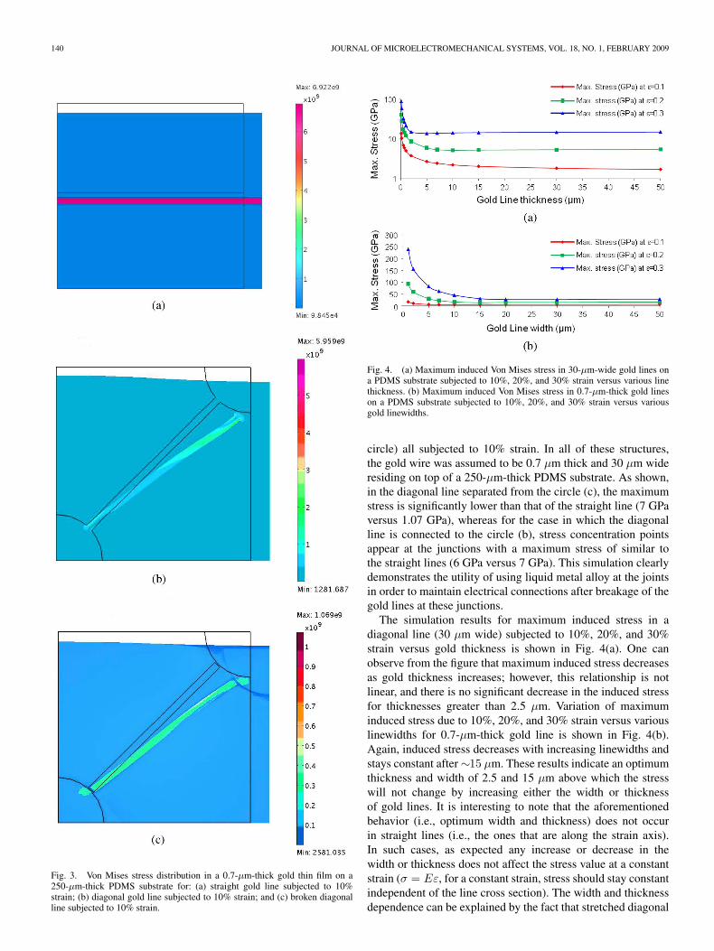
In spite of the difficulty in predicting the ultimate strengthof gold films bonded to an elastomeric substrate, one can gainvaluable insight by simulating several different configurations/conditions. Fig. 3 shows the stress pattern for a straight line,a diagonal line connected to a circle, and a diagonal linedisconnected at the maximum stress points (junction to the
140 JOURNAL OF MICROELECTROMECHANICAL SYSTEMS, VOL. 18, NO. 1, FEBRUARY 2009
Fig. 3. Von Mises stress distribution in a 0.7-µm-thick gold thin film on a250-µm-thick PDMS substrate for: (a) straight gold line subjected to 10%strain; (b) diagonal gold line subjected to 10% strain; and (c) broken diagonalline subjected to 10% strain.
Fig. 4. (a) Maximum induced Von Mises stress in 30-µm-wide gold lines ona PDMS substrate subjected to 10%, 20%, and 30% strain versus various linethickness. (b) Maximum induced Von Mises stress in 0.7-µm-thick gold lineson a PDMS substrate subjected to 10%, 20%, and 30% strain versus variousgold linewidths.
circle) all subjected to 10% strain. In all of these structures,the gold wire was assumed to be 0.7 μm thick and 30 μm wideresiding on top of a 250-μm-thick PDMS substrate. As shown,in the diagonal line separated from the circle (c), the maximumstress is significantly lower than that of the straight line (7 GPaversus 1.07 GPa), whereas for the case in which the diagonalline is connected to the circle (b), stress concentration pointsappear at the junctions with a maximum stress of similar tothe straight lines (6 GPa versus 7 GPa). This simulation clearlydemonstrates the utility of using liquid metal alloy at the jointsin order to maintain electrical connections after breakage of thegold lines at these junctions.
The simulation results for maximum induced stress in adiagonal line (30 μm wide) subjected to 10%, 20%, and 30%strain versus gold thickness is shown in Fig. 4(a). One canobserve from the figure that maximum induced stress decreasesas gold thickness increases; however, this relationship is notlinear, and there is no significant decrease in the induced stressfor thicknesses greater than 2.5 μm. Variation of maximuminduced stress due to 10%, 20%, and 30% strain versus variouslinewidths for 0.7-μm-thick gold line is shown in Fig. 4(b).Again, induced stress decreases with increasing linewidths andstays constant after ∼15 μm. These results indicate an optimumthickness and width of 2.5 and 15 μm above which the stresswill not change by increasing either the width or thicknessof gold lines. It is interesting to note that the aforementionedbehavior (i.e., optimum width and thickness) does not occurin straight lines (i.e., the ones that are along the strain axis).In such cases, as expected any increase or decrease in thewidth or thickness does not affect the stress value at a constantstrain (σ = Eε, for a constant strain, stress should stay constantindependent of the line cross section). The width and thicknessdependence can be explained by the fact that stretched diagonal

KIM et al.: BIAXIAL STRETCHABLE INTERCONNECT WITH LIQUID-ALLOY-COVERED JOINTS ON ELASTOMERIC SUBSTRATE 141
Fig. 5. Deformation of (top) 10- and (bottom) 30-µm-wide lines subjected to20% strain.
lines deform laterally in such a way to accommodate theapplied stress. Thinner and narrower lines deform more henceresulting in the aforementioned behavior. Fig. 5 shows 10- and30-μm-wide lines subjected to 20% strain. As shown, the 10 μmline deforms to an S shape configuration with more pronouncedcurvatures than the 30-μm-wide line (maximum stress for the10-μm line is ∼16 GPa, whereas the 30-μm line sustains amaximum stress of ∼5 GPa).
Finally, before discussing the fabrication process, it is in-structive to calculate the total resistance of the interconnection.Fig. 6(a) shows the schematic of an interconnect segment.Resistivity of Ga/In liquid alloy (20 μΩ · cm) is almost tentimes higher than that of gold (2.2 μΩ · cm); however, thethickness of liquid alloy circle (140 μm in our design) is200 times larger than that of gold (0.7 μm in our design).Therefore, the calculated resistance value of the gold circle ismuch higher than that of liquid alloy plug (R1 � R2); hence,the resistance of gold circle can be ignored since it is in parallelwith the liquid alloy. Gold lines and liquid alloy circles areconnected in series with the resistance of the circles being muchsmaller than that of lines (R � R2, alloys of 200-μm diameter
Fig. 6. Resistance network of a stretchable interconnect. (a) Resistance ofeach component. (b) Simplified total resistance of interconnect.
and 140-μm height as compared to 1000-μm gold straight lineshaving 30-μm width and 0.7-μm thickness). Fig. 6(b) showsa simplified model for the total resistance of the stretchableinterconnects. As argued above, the straight gold line segmentsdominate the resistance with the resistance value for eachsegment being R/2. In addition, the existence of multiple pathsincreases the interconnects current-carrying capacity.
III. FABRICATION PROCESS
A schematic view of the fabrication process is shown inFig. 7. A thin gold film (2000 Å) was first deposited on asilicon wafer (100 p-type). As will be seen later, this gold layerallows an easy separation of the final structure. Fresh PDMS(Sylgard 184, Dow corning, mixing ratio = 10 : 1) was pre-pared and spun coated on gold-deposited silicon wafer at200 r/min for 1 min (thickness of PDMS after curing for10 min in 90 ◦C oven was around 480 μm) [Fig. 7(a)]. A goldfilm of 0.7 μm was then directly deposited on the base PDMSlayer without any adhesion layer [Fig. 7(b)]. Deposited goldfilm was then patterned to form 2-D diamond-shaped tracesusing wet etchant (TFA, Transene Company, Inc.) [Fig. 7(c)].
A second PDMS layer was separately prepared by castingonto a SU-8 (Microchem Corporation, Newton, MA) master(SU-8 2100 was spun coated onto a silicon wafer at 2000 r/minfor 30 s, and patterned through standard lithography). Thethickness of fabricated SU-8 master was ∼140 μm. Prior toPDMS casting, the SU8 surface was treated with trichlorosi-lane (Sigma-Aldrich Corporation) for easy release [13]. FreshPDMS (mixing ratio = 10 : 1) was casted onto the SU-8mold and cured at room temperature for 48 h. Lower curingtemperature reduced the deformation (shrinkage) of thePDMS [14]. A transparency film was then used to form

142 JOURNAL OF MICROELECTROMECHANICAL SYSTEMS, VOL. 18, NO. 1, FEBRUARY 2009
Fig. 7. Fabrication process for biaxial stretchable interconnect. (a) Goldsacrificial film and first PDMS layer deposition. (b) Gold interconnect layerdeposition. (c) Gold interconnect layer patterning. (d) Bonding of the secondPDMS layer with reservoir holes. (e) Screen printing of room-temperatureliquid alloy onto the holes. (f) Attaching the third PDMS layer. (g) Releasingthe structure from the silicon wafer.
SU-8 master/PDMS/transparency stack, which was subse-quently pressurized with a heavy weight (∼2-lb steel) [15].After curing, PDMS was detached from the SU-8 mold. Athin PDMS membrane (∼10 μm thick) still remained afterpeeling off even though a heavy weight was applied duringthe curing process. This thin PDMS membrane was removedthrough a wet etching (Tetrabutylammonium fluoride andN-Methylpyrrolidinone, 3:1, v/v, NMP/75% TBAF in water)step [16]. The second PDMS was bonded to the first one withthe circular openings aligned to the gold line intersectionson the first PDMS layer using a microscopic flip-chip aligner[Fig. 7(d)].
Each hole was then filled with room-temperature liquidalloy (Gallium/Indium = 75.5/24.5, Indium Corporation, liq-uidus temperature ≥ 15.7 ◦C) by screen printing technique[Fig. 7(e)]. Alternatively, one can fill the holes with an auto-mated dispenser. The base metallic gold trace is necessary inorder to fill the holes since room-temperature liquid alloy doesnot wet the PDMS layer. After screen printing, the surface of thesecond PDMS was cleaned with isopropyl alcohol to removethe liquid alloy residues. The cured third PDMS layer (1 mmthick, using a rubber spacer to control the thickness) was then
Fig. 8. Fabricated 2-D diamond-shaped stretchable interconnect.
attached on top of the second layer to cap the whole structure[Fig. 7(f)]. Finally, the fabricated structure was released fromthe silicon wafer by dripping tap water onto the Au-siliconinterface [Fig. 7(g)] [17]. Fig. 8 shows an optical micrographof the fabricated biaxial stretchable interconnect.
The fabrication method outlined above was meant to demon-strate a proof of concept and can be used in small scalelaboratory settings. However, one can envision an automatedmanufacturing process capable of roll-to-roll production ofstretchable interconnects. An example would be sheets of elas-tomeric substrates (this does not have to be PDMS as long asit has desirable stretchability) onto which interconnect layercan be deposited through a shadow mask using a vacuumweb coater. Liquid alloy holes then can be filled through aninked roller blade. Some of these methods are currently usedto manufacture flexible displays and other low-cost organicelectronics.
IV. TEST AND CHARACTERIZATION
A. Measurement Setup
Fabricated stretchable interconnects were bridged over twomicropositioning stages (Newport 460 A, 13-mm travel range)on an optical table. Mounting blocks were placed on eachend of PDMS platform and tightened with screws for stableclamping. Fixed stretchable interconnect was then stretched inone-direction by using a micromanipulator (increasing the dis-tance between micropositioning stages). Four-point resistancemeasurements were performed to cancel out the resistance ofexternal measurement wires and their contact resistance withthe liquid alloy reservoirs. To measure the resistance variations,a constant current of 30 mA was applied to interconnect, and thevoltage variations were recorded by a high-precision voltmeterat incremental lengths of ΔL.
B. Measured Data and Discussion
Since it is well known that Ga alloys react with many metals,before any actual stretch experiment, we measured the goldsheet resistance (ρs) before and after applying Ga/In liquidalloy. Four-point probe method was used for measuring sheetresistance [Fig. 9(a)]. Applied voltage was chosen to be 5 V,and the value of R14 was fixed at 1 kΩ. Sheet resistance can becalculated using
ρs ≈ π
ln(2)× V23
I14= 4.523 × V23
I14(3)
where I14 is the current through R14. Table I shows measuredvoltages, currents, and calculated sheet resistances before and
KIM et al.: BIAXIAL STRETCHABLE INTERCONNECT WITH LIQUID-ALLOY-COVERED JOINTS ON ELASTOMERIC SUBSTRATE 143
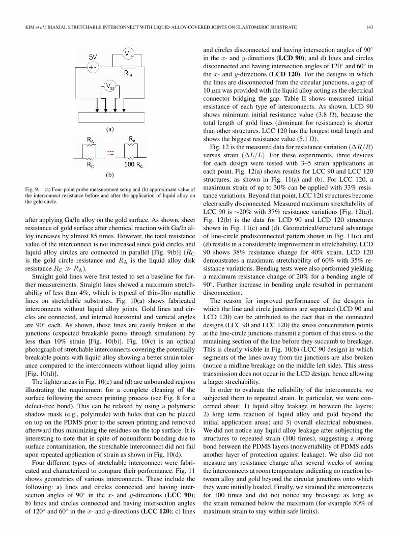
Fig. 9. (a) Four-point probe measurement setup and (b) approximate value ofthe interconnect resistance before and after the application of liquid alloy onthe gold circle.
after applying Ga/In alloy on the gold surface. As shown, sheetresistance of gold surface after chemical reaction with Ga/In al-loy increases by almost 85 times. However, the total resistancevalue of the interconnect is not increased since gold circles andliquid alloy circles are connected in parallel [Fig. 9(b)] (RC
is the gold circle resistance and RA is the liquid alloy diskresistance RC � RA).
Straight gold lines were first tested to set a baseline for fur-ther measurements. Straight lines showed a maximum stretch-ability of less than 4%, which is typical of thin-film metalliclines on stretchable substrates. Fig. 10(a) shows fabricatedinterconnects without liquid alloy joints. Gold lines and cir-cles are connected, and internal horizontal and vertical anglesare 90◦ each. As shown, these lines are easily broken at thejunctions (expected breakable points through simulation) byless than 10% strain [Fig. 10(b)]. Fig. 10(c) is an opticalphotograph of stretchable interconnects covering the potentiallybreakable points with liquid alloy showing a better strain toler-ance compared to the interconnects without liquid alloy joints[Fig. 10(d)].
The lighter areas in Fig. 10(c) and (d) are unbounded regionsillustrating the requirement for a complete cleaning of thesurface following the screen printing process (see Fig. 8 for adefect-free bond). This can be relaxed by using a polymericshadow mask (e.g., polyimide) with holes that can be placedon top on the PDMS prior to the screen printing and removedafterward thus minimizing the residues on the top surface. It isinteresting to note that in spite of nonuniform bonding due tosurface contamination, the stretchable interconnect did not failupon repeated application of strain as shown in Fig. 10(d).
Four different types of stretchable interconnect were fabri-cated and characterized to compare their performance. Fig. 11shows geometries of various interconnects. These include thefollowing: a) lines and circles connected and having inter-section angles of 90◦ in the x- and y-directions (LCC 90);b) lines and circles connected and having intersection anglesof 120◦ and 60◦ in the x- and y-directions (LCC 120); c) lines
and circles disconnected and having intersection angles of 90◦
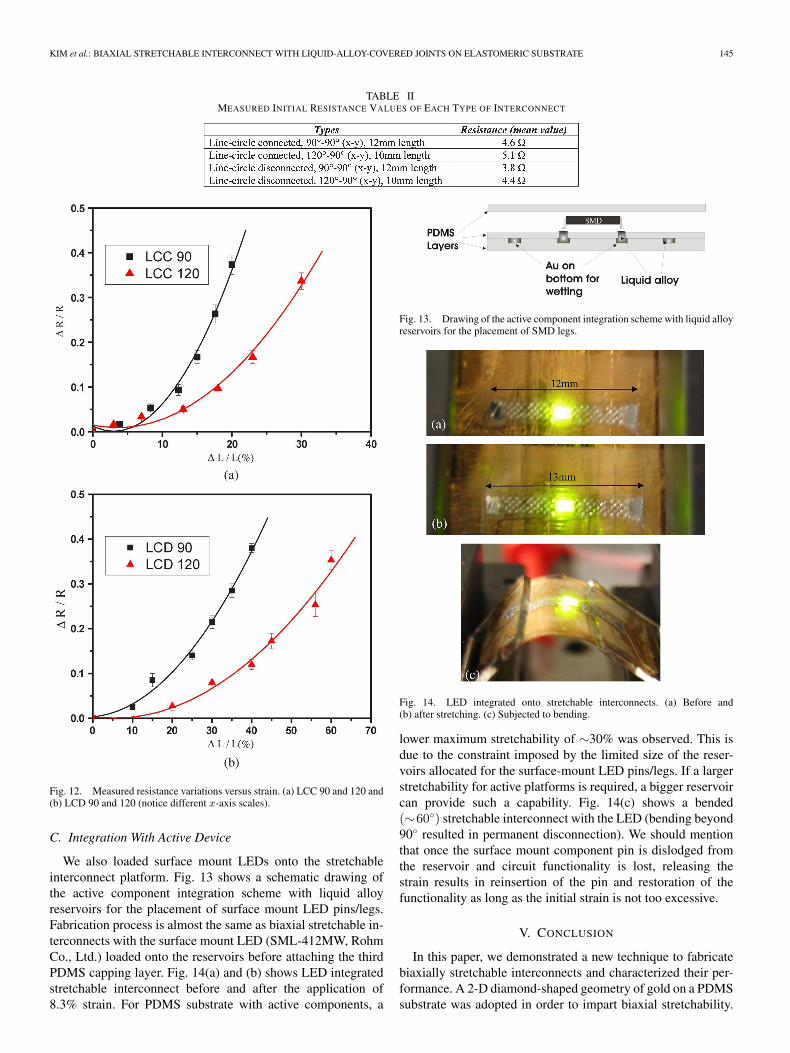
in the x- and y-directions (LCD 90); and d) lines and circlesdisconnected and having intersection angles of 120◦ and 60◦ inthe x- and y-directions (LCD 120). For the designs in whichthe lines are disconnected from the circular junctions, a gap of10 μm was provided with the liquid alloy acting as the electricalconnector bridging the gap. Table II shows measured initialresistance of each type of interconnects. As shown, LCD 90shows minimum initial resistance value (3.8 Ω), because thetotal length of gold lines (dominant for resistance) is shorterthan other structures. LCC 120 has the longest total length andshows the biggest resistance value (5.1 Ω).
Fig. 12 is the measured data for resistance variation (ΔR/R)versus strain (ΔL/L). For these experiments, three devicesfor each design were tested with 3–5 strain applications ateach point. Fig. 12(a) shows results for LCC 90 and LCC 120structures, as shown in Fig. 11(a) and (b). For LCC 120, amaximum strain of up to 30% can be applied with 33% resis-tance variations. Beyond that point, LCC 120 structures becomeelectrically disconnected. Measured maximum stretchability ofLCC 90 is ∼20% with 37% resistance variations [Fig. 12(a)].Fig. 12(b) is the data for LCD 90 and LCD 120 structuresshown in Fig. 11(c) and (d). Geometrical/structural advantageof line-circle predisconnected pattern shown in Fig. 11(c) and(d) results in a considerable improvement in stretchability. LCD90 shows 38% resistance change for 40% strain. LCD 120demonstrates a maximum stretchability of 60% with 35% re-sistance variations. Bending tests were also performed yieldinga maximum resistance change of 20% for a bending angle of90◦. Further increase in bending angle resulted in permanentdisconnection.
The reason for improved performance of the designs inwhich the line and circle junctions are separated (LCD 90 andLCD 120) can be attributed to the fact that in the connecteddesigns (LCC 90 and LCC 120) the stress concentration pointsat the line-circle junctions transmit a portion of that stress to theremaining section of the line before they succumb to breakage.This is clearly visible in Fig. 10(b) (LCC 90 design) in whichsegments of the lines away from the junctions are also broken(notice a midline breakage on the middle left side). This stresstransmission does not occur in the LCD design, hence allowinga larger strechability.
In order to evaluate the reliability of the interconnects, wesubjected them to repeated strain. In particular, we were con-cerned about: 1) liquid alloy leakage in between the layers;2) long term reaction of liquid alloy and gold beyond theinitial application areas; and 3) overall electrical robustness.We did not notice any liquid alloy leakage after subjecting thestructures to repeated strain (100 times), suggesting a strongbond between the PDMS layers (nonwettability of PDMS addsanother layer of protection against leakage). We also did notmeasure any resistance change after several weeks of storingthe interconnects at room temperature indicating no reaction be-tween alloy and gold beyond the circular junctions onto whichthey were initially loaded. Finally, we strained the interconnectsfor 100 times and did not notice any breakage as long asthe strain remained below the maximum (for example 50% ofmaximum strain to stay within safe limits).

144 JOURNAL OF MICROELECTROMECHANICAL SYSTEMS, VOL. 18, NO. 1, FEBRUARY 2009
TABLE IMEASURED VOLTAGE, CURRENT, AND CALCULATED SHEET RESISTANCE
Fig. 10. Photograph of several interconnects. (a) Interconnect without liquid alloy joints (unstretched). (b) Interconnect shown in (a) broken junctions with 10%strain. (c) Interconnect with liquid alloy joints. (d) Stable connection for the interconnect shown in (c) under 20% strain.
Fig. 11. Geometries of four different types of interconnects.
KIM et al.: BIAXIAL STRETCHABLE INTERCONNECT WITH LIQUID-ALLOY-COVERED JOINTS ON ELASTOMERIC SUBSTRATE 145
TABLE IIMEASURED INITIAL RESISTANCE VALUES OF EACH TYPE OF INTERCONNECT
Fig. 12. Measured resistance variations versus strain. (a) LCC 90 and 120 and(b) LCD 90 and 120 (notice different x-axis scales).
C. Integration With Active Device
We also loaded surface mount LEDs onto the stretchableinterconnect platform. Fig. 13 shows a schematic drawing ofthe active component integration scheme with liquid alloyreservoirs for the placement of surface mount LED pins/legs.Fabrication process is almost the same as biaxial stretchable in-terconnects with the surface mount LED (SML-412MW, RohmCo., Ltd.) loaded onto the reservoirs before attaching the thirdPDMS capping layer. Fig. 14(a) and (b) shows LED integratedstretchable interconnect before and after the application of8.3% strain. For PDMS substrate with active components, a
Fig. 13. Drawing of the active component integration scheme with liquid alloyreservoirs for the placement of SMD legs.
Fig. 14. LED integrated onto stretchable interconnects. (a) Before and(b) after stretching. (c) Subjected to bending.
lower maximum stretchability of ∼30% was observed. This isdue to the constraint imposed by the limited size of the reser-voirs allocated for the surface-mount LED pins/legs. If a largerstretchability for active platforms is required, a bigger reservoircan provide such a capability. Fig. 14(c) shows a bended(∼60◦) stretchable interconnect with the LED (bending beyond90◦ resulted in permanent disconnection). We should mentionthat once the surface mount component pin is dislodged fromthe reservoir and circuit functionality is lost, releasing thestrain results in reinsertion of the pin and restoration of thefunctionality as long as the initial strain is not too excessive.
V. CONCLUSION
In this paper, we demonstrated a new technique to fabricatebiaxially stretchable interconnects and characterized their per-formance. A 2-D diamond-shaped geometry of gold on a PDMSsubstrate was adopted in order to impart biaxial stretchability.
146 JOURNAL OF MICROELECTROMECHANICAL SYSTEMS, VOL. 18, NO. 1, FEBRUARY 2009
In addition, potentially breakable points were covered withroom temperature liquid alloy to increase the functionality.Four different geometries having different intersection anglesand line-circle joint structure were designed, fabricated, andcharacterized. A maximum stretchability of 60% with 35%resistance variations was achieved for the 2-D diamond-shapedgold lines separated at circular junctions with intersectionangles of 120◦ and 60◦. Finally, we also demonstrated thepossibility of integrating active components onto the biaxialstretchable interconnect platform with stable functionality uponstretching and bending.
ACKNOWLEDGMENT
The authors would like to thank Dr. K.-S. Lim (Universityof Minnesota), Dr. K. Lee (Purdue University), and H. Park(Purdue University) for their valuable advice and assistance.
REFERENCES
[1] G. P. Crawford, Flexible Flat Panel Displays. Hoboken, NJ: Wiley,2005.
[2] V. J. Lumelsky, M. S. Shur, and S. Wagner, “Sensitive skin,” IEEE SensorsJ., vol. 1, no. 1, pp. 41–51, Jun. 2001.
[3] T. Martin, M. Jones, J. Edmison, and R. Shenoy, “Towards a designframework for wearable electronic textiles,” in Proc. 7th IEEE Int. Symp.Wearable Comput., 2003, pp. 190–199.
[4] A. Nathan and B. R. Chalamala, “Flexible electronics technology,Part II: Materials and devices,” Proc. IEEE, vol. 93, no. 8, pp. 1391–1393,Aug. 2005.
[5] T. Tamai, “Electrical properties of conductive elastomer as electricalcontact material,” IEEE Trans. Compon., Hybrids, Manuf. Technol.,vol. CHMT-5, no. 1, pp. 56–61, Mar. 1981.
[6] S. P. Lacour, J. Jones, Z. Suo, and S. Wagner, “Design and performanceof thin metal film interconnects for skin-like electronic circuits,” IEEEElectron Device Lett., vol. 25, no. 4, pp. 326–334, Apr. 2004.
[7] D. S. Gray, J. Tien, and C. S. Chen, “High-conductivity elastomericelectronics,” Adv. Mater., vol. 16, no. 5, pp. 393–397, Mar. 2004.
[8] N. Chen, J. Engel, S. Pandya, and C. Liu, “Flexible skin with two-axis bending capability made using weaving-by-lithography fabricationmethod,” in Proc. IEEE Int. Conf. MEMS, Istanbul, Turkey, 2006,pp. 330–333.
[9] H.-J. Kim, M. Zhang, and B. Ziaie, “A biaxially stretchable interconnectwith liquid alloy joints on flexible substrate,” in Proc. 14th Int. Conf.Solid-State Sensors Actuators, Lyon, France, Jun. 2007, pp. 1597–1600.
[10] H. Kim, C. Son, and B. Ziaie, “A multiaxial stretchable interconnect usingliquid-alloy-filled elastomeric microchannels,” Appl. Phys. Lett., vol. 92,no. 1, p. 011 904, Jan. 2008.
[11] H. Huang and F. Spaepen, “Tensile testing of free-standing Cu, Ag andAl thin films and Ag/Cu multilayers,” Acta Mater., vol. 48, no. 12,pp. 3261–3269, Jul. 2000.
[12] S. P. Lacour, J. Jones, S. Wagner, T. Li, and Z. Suo, “Stretchableinterconnects for elastic electronic surfaces,” Proc. IEEE, vol. 93, no. 8,pp. 1459–1467, Aug. 2005.
[13] K. W. Roh, K. Lim, H. Kim, and J. H. Hahn, “Poly(dimethylsiloxane)microchip for precolumn reaction and micellar electrokineticchromatography of biogenic amines,” Electrophoresis, vol. 23, no. 7/8,pp. 1129–1137, Apr. 2002.
[14] J.-S. Kim and D. R. Knapp, “Miniaturized multichannel electrosprayionization emitters on poly(dimethylsiloxane) microfluidic devices,”Electrophoresis, vol. 22, no. 18, pp. 3993–3999, Oct. 2001.
[15] B. H. Jo, L. M. Van Lerberghe, K. M. Motsegood, and D. J. Beebe,“Three-dimensional micro-channel fabrication in polydimethylsiloxane(PDMS) elastomer,” J. Microelectromech. Syst., vol. 9, no. 1, pp. 76–81,Mar. 2000.
[16] S. Takayama, E. Ostuni, X. Qian, J. C. McDonald, X. Jiang, P. LeDuc,M. H. Wu, D. E. Ingber, and G. M. Whitesides, “Topographical mi-cropatterning of poly(dimethylsiloxane) using laminar flows of liquids incapillaries,” Adv. Mater., vol. 13, no. 8, pp. 570–574, Apr. 2001.
[17] K. S. Lim, W.-J. Chang, Y.-M. Koo, and R. Bashir, “Reliablefabrication method of transferable micron scale metal pattern forpoly(dimethylsiloxane) metallization,” Lab Chip, vol. 6, no. 4, pp. 578–580, Apr. 2006.
Hyun-Joong Kim received the B.S. and M.S. de-grees in electronics engineering from Inchon Na-tional University, Inchon, Korea, in 1996 and 1998,respectively, the M.S. degree in electrical and com-puter engineering from the University of Minnesota,Minneapolis, in 2004, and the Ph.D. degree in elec-trical and computer engineering from Purdue Univer-sity, West Lafayette, IN, in 2008.
He is currently a Senior Process Engineer withthe Etch and Clean Division, Applied Materials,Sunnyvale, CA, conducting etch process research
and development in DRAM and flash memory devices. His research interestsinclude the design and fabrication of PVDF-based ultrasound transducer arraysand fabrication technology development for stretchable interconnects for flexi-ble electronics.
Teimour Maleki received the B.Sc. degree in bio-medical engineering from Amirkabir University ofTechnology, Tehran, Iran, in 2000, and the M.Sc. de-gree in electrical engineering from the University ofTehran, Tehran, in 2003. He is currently working to-ward the Ph.D. degree in electrical and computer en-gineering at Purdue University, West Lafayette, IN.
From 2001 to 2005, he was a Research Assistantwith the Thin Film Laboratory, University of Tehran,where he worked on MEMS technology (i.e., devel-oped anisotropic etching of silicon and polymers and
created membranes for sensors). Since 2006, he has been a Research Assistantwith the Birck Nanotechnology Center, Purdue University. His research inter-ests include biomedical applications of MEMS and, specifically, implantablewireless sensors.
Pinghung Wei was born in Tainan, Taiwan, in1985. He received the B.S. degree in electrical andcomputer engineering from Purdue University, WestLafayette, IN, in 2006. He is currently working to-ward the Ph.D. degree in electrical and computerengineering at Purdue University.
His research interests include integrated flexi-ble electrode systems and packaging techniques forneural sensing and recording.
Babak Ziaie (A’95–M’00–SM’07) received thePh.D. degree in electrical engineering from the Uni-versity of Michigan, Ann Arbor, in 1994. His dis-sertation was related to the design and developmentof an implantable single-channel microstimulator forfunctional neuromuscular stimulation.
From 1995 to 1999, he was a Postdoctoral Fellowand an Assistant Research Scientist with the Centerfor Integrated Microsystems (CIMS), University ofMichigan. From 1999 to 2004, he was an Assis-tant Professor with the Department of Electrical and
Computer Engineering, University of Minnesota, Minneapolis. Since January2005, he has been with the School of Electrical and Computer Engineering,Purdue University, West Lafayette, IN, where he is currently an AssociateProfessor. His research interests include biomedical applications of MEMS andmicrosystems (BioMEMS), which include implantable wireless microsystems,smart polymers for physiological sensing and active flow control, microma-chined interfaces with the central nervous system, biomimetic sensors andactuators, and ultrasensitive sensors for biological (molecular and cellular)applications.
Dr. Ziaie is a member of the American Association for the Advancement ofScience. He was the recipient of the NSF Career Award in Biomedical Engi-neering (2001) and the McKnight Endowment Fund Award for TechnologicalInnovations in Neuroscience (2002).
Copyright © 2022 FDOKUMEN