

Electrospun TiO2 nanofibre-based gas sensors fabricated by AC electrophoresis deposition
Upload
khangminh22Category
view
0download
0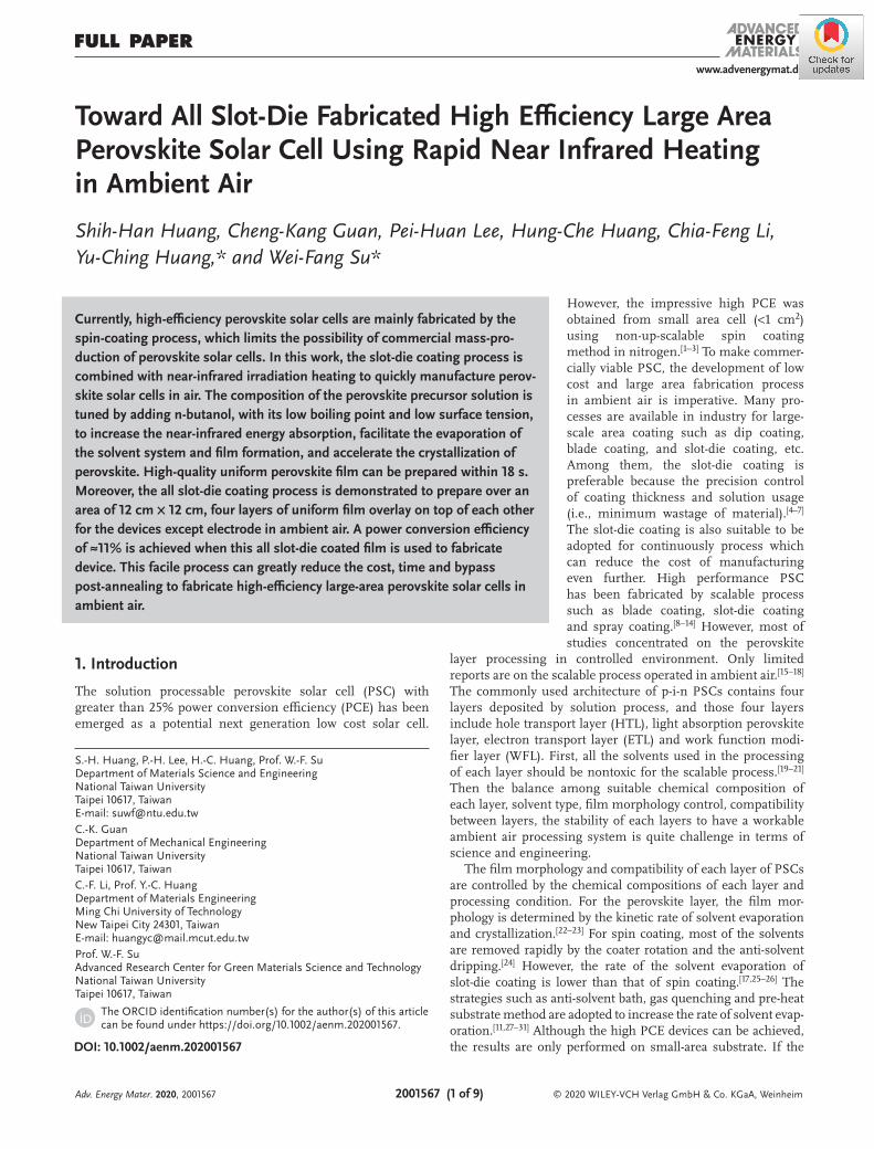
www.advenergymat.de
2001567 (1 of 9) © 2020 WILEY-VCH Verlag GmbH & Co. KGaA, Weinheim
Full PaPer
Toward All Slot-Die Fabricated High Efficiency Large Area Perovskite Solar Cell Using Rapid Near Infrared Heating in Ambient Air
Shih-Han Huang, Cheng-Kang Guan, Pei-Huan Lee, Hung-Che Huang, Chia-Feng Li, Yu-Ching Huang,* and Wei-Fang Su*
DOI: 10.1002/aenm.202001567
However, the impressive high PCE was obtained from small area cell (<1 cm2) using non-up-scalable spin coating method in nitrogen.[1–3] To make commer-cially viable PSC, the development of low cost and large area fabrication process in ambient air is imperative. Many pro-cesses are available in industry for large-scale area coating such as dip coating, blade coating, and slot-die coating, etc. Among them, the slot-die coating is preferable because the precision control of coating thickness and solution usage (i.e., minimum wastage of material).[4–7] The slot-die coating is also suitable to be adopted for continuously process which can reduce the cost of manufacturing even further. High performance PSC has been fabricated by scalable process such as blade coating, slot-die coating and spray coating.[8–14] However, most of studies concentrated on the perovskite
layer processing in controlled environment. Only limited reports are on the scalable process operated in ambient air.[15–18] The commonly used architecture of p-i-n PSCs contains four layers deposited by solution process, and those four layers include hole transport layer (HTL), light absorption perovskite layer, electron transport layer (ETL) and work function modi-fier layer (WFL). First, all the solvents used in the processing of each layer should be nontoxic for the scalable process.[19–21] Then the balance among suitable chemical composition of each layer, solvent type, film morphology control, compatibility between layers, the stability of each layers to have a workable ambient air processing system is quite challenge in terms of science and engineering.
The film morphology and compatibility of each layer of PSCs are controlled by the chemical compositions of each layer and processing condition. For the perovskite layer, the film mor-phology is determined by the kinetic rate of solvent evaporation and crystallization.[22–23] For spin coating, most of the solvents are removed rapidly by the coater rotation and the anti-solvent dripping.[24] However, the rate of the solvent evaporation of slot-die coating is lower than that of spin coating.[17,25–26] The strategies such as anti-solvent bath, gas quenching and pre-heat substrate method are adopted to increase the rate of solvent evap-oration.[11,27–31] Although the high PCE devices can be achieved, the results are only performed on small-area substrate. If the
Currently, high-efficiency perovskite solar cells are mainly fabricated by the spin-coating process, which limits the possibility of commercial mass-pro-duction of perovskite solar cells. In this work, the slot-die coating process is combined with near-infrared irradiation heating to quickly manufacture perov-skite solar cells in air. The composition of the perovskite precursor solution is tuned by adding n-butanol, with its low boiling point and low surface tension, to increase the near-infrared energy absorption, facilitate the evaporation of the solvent system and film formation, and accelerate the crystallization of perovskite. High-quality uniform perovskite film can be prepared within 18 s. Moreover, the all slot-die coating process is demonstrated to prepare over an area of 12 cm × 12 cm, four layers of uniform film overlay on top of each other for the devices except electrode in ambient air. A power conversion efficiency of ≈11% is achieved when this all slot-die coated film is used to fabricate device. This facile process can greatly reduce the cost, time and bypass post-annealing to fabricate high-efficiency large-area perovskite solar cells in ambient air.
S.-H. Huang, P.-H. Lee, H.-C. Huang, Prof. W.-F. SuDepartment of Materials Science and EngineeringNational Taiwan UniversityTaipei 10617, TaiwanE-mail: [email protected]. GuanDepartment of Mechanical EngineeringNational Taiwan UniversityTaipei 10617, TaiwanC.-F. Li, Prof. Y.-C. HuangDepartment of Materials EngineeringMing Chi University of TechnologyNew Taipei City 24301, TaiwanE-mail: [email protected]. W.-F. SuAdvanced Research Center for Green Materials Science and TechnologyNational Taiwan UniversityTaipei 10617, Taiwan
The ORCID identification number(s) for the author(s) of this article can be found under https://doi.org/10.1002/aenm.202001567.
1. Introduction
The solution processable perovskite solar cell (PSC) with greater than 25% power conversion efficiency (PCE) has been emerged as a potential next generation low cost solar cell.
Adv. Energy Mater. 2020, 2001567
www.advenergymat.dewww.advancedsciencenews.com
© 2020 WILEY-VCH Verlag GmbH & Co. KGaA, Weinheim2001567 (2 of 9)
area of the substrate is increased, new processing parameters will need to be optimized. Because of the poor thermal conduc-tivity of glass substrate, the pre-heat substrate method requires long time of at least several minutes to balance the temperature of large-area film evenly using conventional heating which hin-ders the development of continuous process line.
Near-infrared irradiation (NIR) heating is a promising approach for rapid highly efficient heating. Fluorine doped tin oxide (FTO) exhibits high absorption in NIR region. Thus, the high temperature can be reached in a matter of few seconds, as compare with conventional heating.[32–35] The NIR heating was explored by us before to replace conventional heating for post-annealing of perovskite film.[36] This approach leads to the formation of good crystalline perovskite film with high PCE of devices. We would like to further advance the technology using rapid NIR to fabricate high crystalline films of hole transport layer and perovskite layer from wet film to solid film simultane-ously without any post-annealing. The NIR drying the ETL and WFL is also explored.
In this work, we firstly used the rapid NIR heating process to slot-die coat perovskite layer on top of the NiOx layer on FTO substrate with an area of 12 cm × 12 cm. For the purpose to evaluate the film quality for device application, we cut the large-area slot-die coated films into 2 cm × 2 cm, then we fabricated the testing devices with an area of 0.09 cm2. The high quality of large area perovskite layer was prepared by adding n-butanol in the perovskite precursor to enhance its NIR absorption, wet-tability and evaporation through rapid NIR heating. The device can achieve the highest PCE of 14.30% using films of slot-die coated NiOx/perovskite and spin-coated [6,6]-phenyl-C61-butyric acid methyl ester (PCBM)/polyethyleneimine (PEI). Further-more, we used the rapid NIR heating process to successfully fabricate an area of 12 cm × 12 cm four layers of uniform film overlay on top of each other on FTO substrate for p-i-n devices except electrode. The four layers are NiOx as HTL, MAPbI3 as perovskite layer, PCBM as ETL and tetrabutylammonium hydroxide (TBAOH) as WFL. Each layer is uniform prepared
within 20 s except HTL. The activation energy of NiOx crystalli-zation is one order of higher than that of the perovskite layer, [37] so it takes 216 s to process. The fabrication of commonly used PEI as WFL was not successfully deposited by using slot-die regardless hot plate (HP) heating or NIR heating because the isopropyl alcohol (IPA) of PEI solution cannot evaporate off fast enough; it penetrates into PCBM layer and attacks the perov-skite layer. The PEI polymer contains many active hydrogens of primary and secondary amine, which retards the evapora-tion of IPA. On the contrary, TBAOH does not contain active hydrogen as PEI. Thus, TBAOH is a good candidate for WFL in the slot-die process. When four layers of large-area slot-die coated films were used to fabricate devices (area: 0.09 cm2) and module (6 cells in series and unit cell area: 0.63 cm2), the PCE of ≈11% and 10.34% can be obtained, respectively. This simpli-fied process of no post-annealing has potential to become a viable commercial production procedure with fast production rate and energy conservation to meet the demands of low cost, large area and high quality perovskite solar cell.
2. Results and Discussion
All of the films prepared in this study are carried out by solu-tion process of slot-die coating in ambient air. To eliminate the health hazard to the operator during the coating process, we used environmental benign solvents to prepare four coating solutions. The selection of solvents were determined according to Hansen solubility parameter and donor number of sol-vents.[19–21] There are ethanol for NiOx HTL, a solvent mixture (1:9 by vol%) of γ-butylrolactone (GBL) and dimethyl sulfoxide (DMSO) for perovskite layer, o-xylene for PCBM and isopro-panol for WFL of PEI or TBAOH. To demonstrate the novelty of rapid NIR heating over thermal heating for large-area slot-die coating process, we carried out in parallel of the two heating methods: HP and NIR. The structures of device and slot-die machine are shown in Figure 1a,b, respectively. Figure 1c,d
Figure 1. a) Device structure of PSCs, and b) slot-die coating machine with NIR heating. Schematic diagram of slot-die coated perovskite layer fabri-cated by c) hot plate heating (HP-PSC) and d) NIR heating (NIR-PSC). J–V curves of PSCs with e) HP-PSCs and f) NIR-PSCs.
Adv. Energy Mater. 2020, 2001567
www.advenergymat.dewww.advancedsciencenews.com
© 2020 WILEY-VCH Verlag GmbH & Co. KGaA, Weinheim2001567 (3 of 9)
illustrates the schematic diagrams of two heating methods for slot-die coating. The J–V curves of the devices fabricated using either hot-plate (HP-PSCs) or NIR (NIR-PSCs) processed film are shown in Figure 1e,f, respectively. The relative photovoltaic characteristics are summarized in Tables 1 and 2. We tuned the temperature of hot plate from 110 to 180 °C, and we can observe the hot plate temperature is very critical to the PCE of HP-PSCs (Figure 1e). When the temperature of hot plate is higher than 150 °C, the PSCs exhibit the PCE over 10%, the highest PCE of 13.09% is achieved at the temperature of 170 °C. As the hot plate temperature is lower than 130 °C, the Voc of slot-die coated PSCs dramatically reduces to <0.5 V, and thus resulted in the low PCE of <4%. Figure S1 (Supporting Information) shows photographic images of the perovskite films deposited on 4 cm × 4 cm NiOx coated FTO substrate at different hot-plate tem-perature. The photos were taken by look over the film through the ceiling fluorescent lights. The film deposited below 130 °C exhibits a very rough surface morphology and extremely nonuniform. Such a rough layer makes the subsequent layers, like PCBM and PEI, difficult to be deposited completely on top of the perovskite layer, and thus reduced the Voc greatly.[6] Our previous study indicated that the thermal energy from NIR irradiation is mainly absorbed by the FTO substrate when the NIR heating was used to anneal NiOx layer. [38] Therefore, we firstly tuned the NIR irradiation time to make the tempera-ture of the NIR-heated FTO substrate close to the hot plate temperature. Temperature of FTO substrate was obtained by directly measuring the FTO surface with a thermocouple. The temperature of NIR-heated FTO substrate corresponding to the different NIR irradiation time is summarized in Table S1 (Supporting Information). Figure 1f shows the PCEs of slot-die coated PSCs by using NIR heating process. The PCEs of the slot-die coated PSCs gradually enhance with the increasing
NIR irradiation time, and the highest PCE of NIR-PSCs can be achieved to ≈10% as the NIR irradiation time is 17.5 s. Although the PCE of the NIR-slot-die coated PSCs is still lower than that of HP-slot-die coated PSCs, the result still demonstrates that the NIR heating process has potential in slot-die coated PSCs.
The transformation time from wet film to solid film is critical to achieve high crystalline perovskite, thus high PCE of PSC. Therefore, we adjusted the transformation time care-fully by using hot plate or NIR to heat the FTO substrate as shown in the above study. The efficiency of NIR heating pro-cess is mainly related to the extent of NIR absorption of the heated materials. In addition to the FTO substrate, the solvent used in the perovskite precursor solution absorbs NIR irradia-tion energy as well. The difference in heat transfer of thermal heating and NIR heating is illustrated in Figure 2a. The NIR energy absorbed by perovskite precursor solution heats the perovskite wet film directly and thus accelerates the transfor-mation of wet film to dry film. Therefore, we speculate that if the solvent used in the perovskite precursor can absorb the NIR energy very effectively, the PCE of PSCs using NIR-slot-die coated films can be further improved. Figure 2b shows the NIR irradiation wavelength and absorption spectrum of glass, FTO, DMSO and GBL, and the DMSO and GBL are the host solvents for the perovskite precursor solution. From the absorp-tion spectrum, we can find that DMSO and GBL absorb some NIR irradiation energy as well. We would like to add other sol-vents in the perovskite precursor to increase their NIR absorp-tion; however, one needs to note that the perovskite precursor solution made from the ternary solvents should exhibit good solution stability. The alcoholic solvent was chosen as the ter-nary solvent for the perovskite precursor due to its large absorp-tion at 1400–1800 nm and its low surface tension for good film wettability. Both methanol and n-butanol can increase the absorption in NIR region, but the addition of methanol made the perovskite precursor precipitated out easily (Figure S2, Sup-porting Information). Thus, we selected n-butanol as ternary solvent in the following study, and the absorption spectrum of n-butanol is shown in Figure 2b. The effects of n-butanol on the characteristics of precursor solution, film and crystal forma-tion of perovskite are carefully investigated. First, we studied the changes of absorption of perovskite precursor solution by varying the amount of n-butanol from 0 to 50 vol%. The absorption spectrum of each solution is very similar; however, the precipitation occurs with the solution containing 20 vol% n-butanol as shown in Figure S3a (Supporting Information). Then, we evaluated the effects of n-butanol amount on the changes of crystal structure of perovskite using X-ray diffraction (XRD). Figure S3b (Supporting Information) shows that the intensity of perovskite peak at 14.10° is reduced and the inten-sity of PbI2 peak at 12.67° is increased after adding more than 10 vol% n-butanol. Furthermore, the presence of precipitate at high concentration, indicates that the solubility of n-butanol in perovskite precursor solution is limited. The formation of complex from precursor and solvents was examined by Fourier-transform infrared spectroscopy (FTIR). We prepared the com-plex by adding anti-solvent of chloroform into the precursor solution containing different amount of n-butanol. Figure S3c (Supporting Information) reveals the characteristic IR peaks of the complex was not shifted with the addition of n-butanol
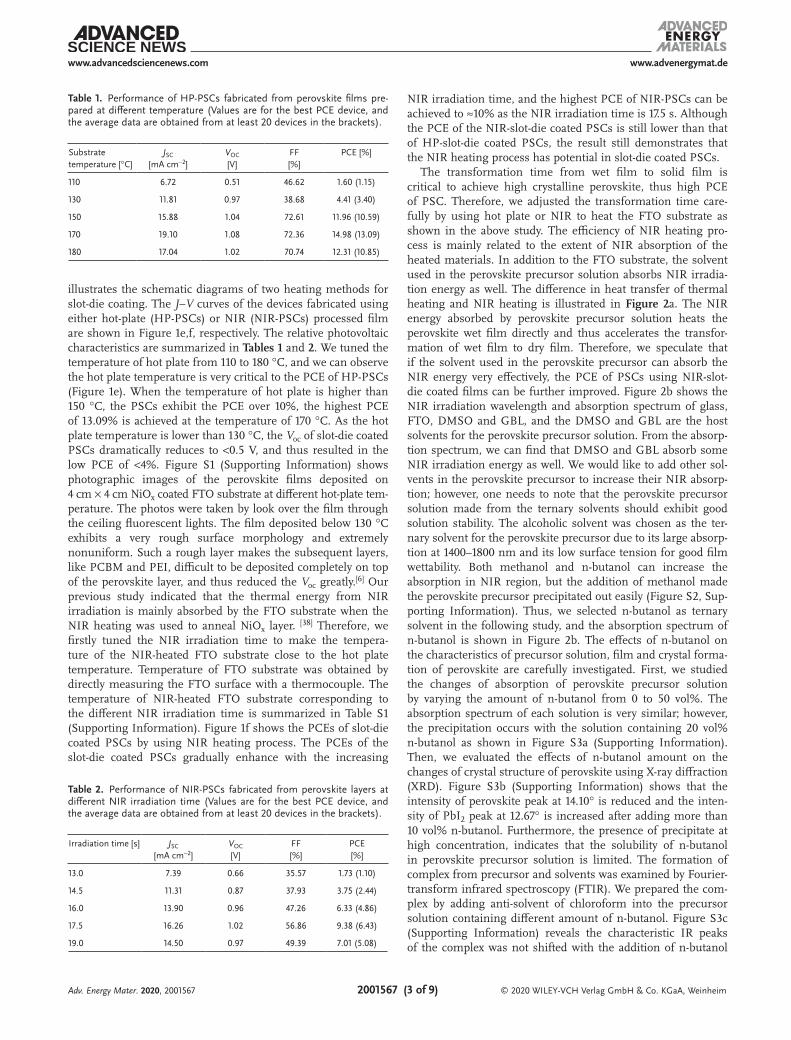
Table 1. Performance of HP-PSCs fabricated from perovskite films pre-pared at different temperature (Values are for the best PCE device, and the average data are obtained from at least 20 devices in the brackets).
Substrate temperature [°C]
JSC [mA cm−2]
VOC [V]
FF [%]
PCE [%]
110 6.72 0.51 46.62 1.60 (1.15)
130 11.81 0.97 38.68 4.41 (3.40)
150 15.88 1.04 72.61 11.96 (10.59)
170 19.10 1.08 72.36 14.98 (13.09)
180 17.04 1.02 70.74 12.31 (10.85)
Table 2. Performance of NIR-PSCs fabricated from perovskite layers at different NIR irradiation time (Values are for the best PCE device, and the average data are obtained from at least 20 devices in the brackets).
Irradiation time [s] JSC [mA cm−2]
VOC [V]
FF [%]
PCE [%]
13.0 7.39 0.66 35.57 1.73 (1.10)
14.5 11.31 0.87 37.93 3.75 (2.44)
16.0 13.90 0.96 47.26 6.33 (4.86)
17.5 16.26 1.02 56.86 9.38 (6.43)
19.0 14.50 0.97 49.39 7.01 (5.08)
Adv. Energy Mater. 2020, 2001567

www.advenergymat.dewww.advancedsciencenews.com
© 2020 WILEY-VCH Verlag GmbH & Co. KGaA, Weinheim2001567 (4 of 9)
which implies that there is no complex formation.[39–41] Thus the low boiling point of n-butanol facilitate the evaporation of ternary solvent system and accelerate the crystallization of perovskite. Therefore, the amount of n-butanol was optimized and fixed at 10 vol%. The perovskite precursor solution was pre-pared using the ternary solvent mixture of GBL:DMSO:n-butanol (1:8:1 vol%) in the following study. The J–V curves and related photovoltaic characteristics of devices fabricated from perov-skite films prepared from this solvent system are shown in Figure 3a and Table 3, respectively. Within 14.5 s NIR irradia-tion, the PCE of device can be increased from 3.75% to 10.31% using the perovskite layer fabricated from precursor solution containing n-butanol. These results prove our speculation of increased NIR absorption from n-butanol. The PCE of devices can be further increased to 12.13% with a longer irradiation of 16 s by enhancing the evaporation and crystallization of perov-skite layer. Figure S4 (Supporting Information) shows the SEM images of NIR-slot-die coated perovskite films from two dif-ferent solvent compositions of perovskite precursor solution at
different NIR irradiation time. These results show that the films fabricated from the solution of ternary solvent system exhibit denser morphology in a shorter irradiation time. Moreover, the larger perovskite grain presented in the films indicates the fast growth of perovskite crystal using the precursor solution con-taining n-butanol because more NIR energy was absorbed by solution. Furthermore, all the NIR-slot-die coated PSCs fabri-cated using this precursor solution of ternary solvent system have high Voc, implying the good surface coverage of the NIR-slot-die coated perovskite layer. For comparison, the ternary solvent system was also investigated in the hot plate heating process. Figure 3b show the J–V curves of devices fabricated using different solution composition and different heating methods. The detailed processing parameters and photovoltaic characteristics are shown in Table S2 (Supporting Information). The HP-slot-die coated devices fabricated from the precursor solution of ternary solvent system exhibit a similar PCE trend as compared to the devices from the binary solvent system, which indicates that the n-butanol has little effect on the PCE
Figure 2. a) Schematic diagrams of two kinds of heating methods. b) NIR irradiation wavelength and absorption spectra of FTO and solvents.
Figure 3. a) J–V curves of NIR-PSCs fabricated from perovskite film prepared by precursor containing 10 vol% n-butanol at different NIR irradiation time. b) J–V curves of NIR-PSC and HP-PSC fabricated from perovskite films prepared by different perovskite precursor solutions.
Adv. Energy Mater. 2020, 2001567

www.advenergymat.dewww.advancedsciencenews.com
© 2020 WILEY-VCH Verlag GmbH & Co. KGaA, Weinheim2001567 (5 of 9)
of PSCs fabricated by the hot-plate process. The results further confirm the improved PCE of PSCs by NIR heating is due to increased NIR absorption from n-butanol.
To further study the effect of n-butanol addition on the phys-ical characteristics of slot-die coated films and devices, we con-ducted detailed investigations using photoluminescence (PL), time-resolved PL (TRPL), atomic force microscopy (AFM), and XRD. Figure 4a shows the addition of n-butanol has little effect on the PL intensity of HP-slot-die coated films. On the contrary, the PL intensity of NIR-slot-die coated films can be enhanced by adding 10 vol% n-butanol. The increased PL intensity implies that the film quality of NIR-slot-die coated film is improved using ternary system, which is consistent with the results of PCE (Table S2, Supporting Information). We further used TRPL to determine the charge carrier lifetime of these perovskite films fabricated with and without n-butanol, as shown in Figure 4b.
The decays follow a second-order exponential decay, and the car-rier lifetime (τavg) is obtained by fitting data, according to litera-ture.[42] The τavg of HP-slot-die coated perovskite films fabricated from the precursors with and without 10 vol% n-butanol does not change much at 31.95 and 33.60 ns, respectively. Thus, the quality of the film by HP does not improve using n-butanol. The τavg of NIR-slot-die coated perovskite films are 2.96 and 14.84 ns respectively for the films fabricated from the precursors without and with 10 vol% n-butanol.
The addition of low surface tension n-butanol is expected to improve the wettability of precursor solution on the NiOx coated FTO substrate during the slot-die coating process. The proper-ties of solvents in the ternary system are summarized in Table S3 (Supporting Information). Figure S5 (Supporting Informa-tion) shows the measurements of contact angle of the films fabricated from different concentration perovskite precursor containing 10 vol% n-butanol. The contact angles for precursor solutions are indeed reduced by the addition n-butanol. Thus, smoother films are expected. Figure 4c shows the AFM images of the slot-die coated films. The HP-slot-die coated films have large crystals, which may imply the film is denser than the NIR-slot-die coated films. The results are consistent with the higher carrier lifetime of HP-slot-die coated films from the study of PL and TRPL. The roughness of HP-slot-die coated film is slightly reduced from 88.4 to 83.5 nm using n-butanol. The roughness of NIR-slot-die coated film was greatly reduced from 78.4 to 50.1 nm with less defects using n-butanol. Thus, the rough-ness of slot-die coated films is reduced using n-butanol. The XRD patterns of slot-die coated films are shown in Figure 4d. The crystallization characteristics of the HP-slot-die coated
Table 3. Performance of NIR-PSCs fabricated from perovskite layers pre-pared using precursor solution containing 10 vol% n-butanol at different NIR irradiation time (Values are for the best PCE device, and the average data are obtained from at least 20 devices in the brackets).
Irradiation time [s]
JSC [mA cm−2]
VOC [V]
FF [%]
PCE [%]
13.0 10.84 0.94 36.63 3.73 (2.10)
14.5 15.12 0.98 69.34 10.31 (7.31)
16.0 15.52 1.05 74.33 12.13 (9.61)
17.5 14.26 1.04 70.95 10.55 (8.21)
19.0 13.00 1.03 33.56 4.50 (2.92)
Figure 4. Characterization of HP-slot-die coated perovskite films and NIR-perovskite films fabricated from the solution without and with 10 vol% n-butanol a) PL spectra, b) TRPL spectra, c) AFM images, and d) XRD patterns.
Adv. Energy Mater. 2020, 2001567
www.advenergymat.dewww.advancedsciencenews.com
© 2020 WILEY-VCH Verlag GmbH & Co. KGaA, Weinheim2001567 (6 of 9)
perovskite films are not affected using n-butanol. In contrast, the intensity of XRD peaks of perovskite is increased but the intensity of PbI2 peak is decreased for the NIR-slot-die coated perovskite films using n-butanol. In a short summary, the addi-tion of low boiling point and low surface tension n-butanol in perovskite precursor solution increases the NIR absorp-tion, facilitates the evaporation of ternary solvent system and accelerates the crystallization of perovskite using rapid NIR. In Figure S6 (Supporting Information), the unencapsulated devices were stored in dry air (25 °C and RH 30–40%). After 220 h, the PCE of NIR-PSCs fabricated from without and with 10 vol% n-butanol were remained at 64% and 87% of the initial PCE, respectively. It implies that adding n-butanol improves the morphology and crystal structure of perovskite films fabricated by NIR heating. Compare to HP-PSCs, the PCE can be main-tained over 93% of the initial PCE due to the larger grain size of the perovskite film, which expects to have better long-term stability.
The PCEs of devices significantly improve to ≈12% from NIR-slot-die coated perovskite layer prepared by precursor solu-tion containing n-butanol. The thickness of the perovskite layer is about 700 nm, which is obviously thicker than the optimal thickness of perovskite layer by spin coating (300–400 nm).[38] Therefore, we tried to adjust the coating parameters of slot-die process to further increase the device performance by lowering the thickness to 350 nm. Table S4 and Figure S7 (Supporting
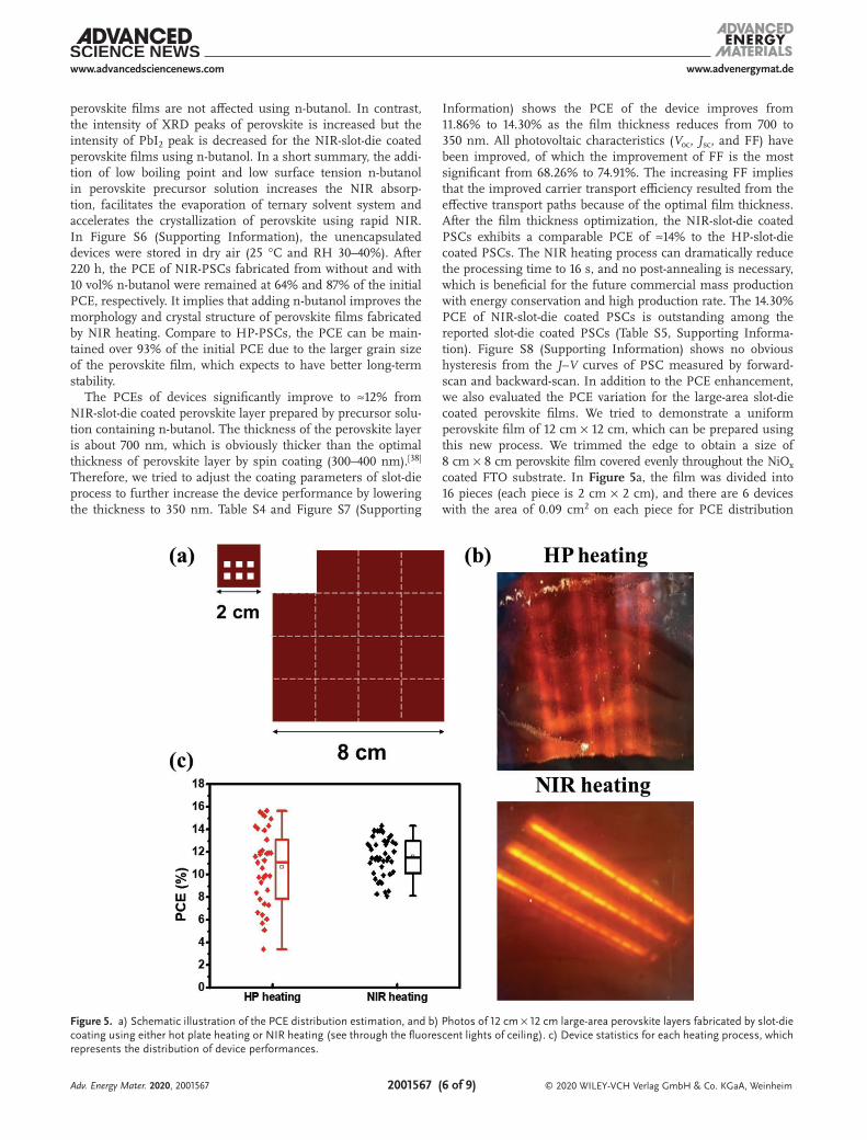
Information) shows the PCE of the device improves from 11.86% to 14.30% as the film thickness reduces from 700 to 350 nm. All photovoltaic characteristics (Voc, Jsc, and FF) have been improved, of which the improvement of FF is the most significant from 68.26% to 74.91%. The increasing FF implies that the improved carrier transport efficiency resulted from the effective transport paths because of the optimal film thickness. After the film thickness optimization, the NIR-slot-die coated PSCs exhibits a comparable PCE of ≈14% to the HP-slot-die coated PSCs. The NIR heating process can dramatically reduce the processing time to 16 s, and no post-annealing is necessary, which is beneficial for the future commercial mass production with energy conservation and high production rate. The 14.30% PCE of NIR-slot-die coated PSCs is outstanding among the reported slot-die coated PSCs (Table S5, Supporting Informa-tion). Figure S8 (Supporting Information) shows no obvious hysteresis from the J–V curves of PSC measured by forward-scan and backward-scan. In addition to the PCE enhancement, we also evaluated the PCE variation for the large-area slot-die coated perovskite films. We tried to demonstrate a uniform perovskite film of 12 cm × 12 cm, which can be prepared using this new process. We trimmed the edge to obtain a size of 8 cm × 8 cm perovskite film covered evenly throughout the NiOx coated FTO substrate. In Figure 5a, the film was divided into 16 pieces (each piece is 2 cm × 2 cm), and there are 6 devices with the area of 0.09 cm2 on each piece for PCE distribution
Figure 5. a) Schematic illustration of the PCE distribution estimation, and b) Photos of 12 cm × 12 cm large-area perovskite layers fabricated by slot-die coating using either hot plate heating or NIR heating (see through the fluorescent lights of ceiling). c) Device statistics for each heating process, which represents the distribution of device performances.
Adv. Energy Mater. 2020, 2001567

www.advenergymat.dewww.advancedsciencenews.com
© 2020 WILEY-VCH Verlag GmbH & Co. KGaA, Weinheim2001567 (7 of 9)
estimation. Figure 5b,c shows the pictures of the large-area perovskite films deposited either by HP-slot-die or NIR-slot-die process, and the corresponding PCE distribution. Compared with the HP-slot-die coated film, the NIR-slot-die coated film exhibits high uniformity, and its efficiency distribution is nar-rower. We speculate that there is a certain degree of FTO thick-ness difference when the large-area FTO deposited on a glass substrate. The FTO thickness variation would result in dif-ferent heat transfer capabilities at various points of large-area FTO substrate. However, the NIR heating process is to directly heat the perovskite wet film, so the heat uniformity is mainly affected by the film thickness of perovskite layer. If the uni-formity of slot-die coated film can be well controlled, the PCE variation can be effectively minimized. Therefore, our results show that the NIR-heating process is more suitable for large-area and rapid commercial mass production manufacture. Fur-thermore, we also fabricated large-area module of 4 cm × 4 cm consisting of six cells (0.3 cm × 2.1 cm for each cell) connected in series by the NIR-heated slot-die coated process. The pic-ture and the related J–V curve of the module are shown in Figure 6a. The module exhibits a promising PCE of 10.34% with Voc of 5.73 V, Jsc of 2.85 mA cm−2, and FF of 63.34%. The reducing PCE of module may be resulted from the connected loss of each cell and the resist loss caused by the long carrier transport path on the large-area FTO substrate.
As a final goal of this research, we would like to demon-strate all slot-die coated PSCs. The abovementioned studies were mainly focus on the optimization of the slot-die param-eters for the perovskite layer in the device structure of FTO/NiOx/Perovskite/PCBM/PEI/Ag. We further investigated the slot-die coated PCBM layer and PEI layer separately. The J–V curves and performance are presented in Figure 6b and Table S6 (Supporting Information). When the devices with a slot-die coated PCBM layer and spin-coated PEI layer, the PCE of the devices is 11.42% with Voc of 1.04 V, Jsc of 17.01 mA cm−2, and FF of 64.57%. Then, we slot-die coated the PEI layer on top of the PCBM layer to complete the fully slot-die coated devices, but the PCE of all slot-die coated PSCs is significantly reduced to 6.74% due to the decreasing FF and Voc. The chemical structure of PEI (Figure S9, Supporting Information) contains many active hydrogens from primary amine and secondary amine functional groups, which are highly reactive toward perovskite materials.[43] The low FF and Voc are resulted from this action. This phenomenon is not observed for spin-coated PEI due to
the short residence time on top of the perovskite/PCBM layer. However, when the PEI layer is deposited by slot-die coating, the time from wet film to dry film is long enough to let the solution reacting with the adjacent layer. Therefore, this result indicates that the PEI is not suitable for the slot-die coated process. As shown in Figure S9 (Supporting Information), TBAOH does not contain active hydrogen as PEI. Thus, we replaced the PEI by TBAOH, the PCE of 10.96% is reached for the devices fabricated from all slot-die coated four layers on FTO substrate. The result is similar to that of devices fabricated from slot-die coated three layers plus spin-coated PEI (Table S6, Supporting Information). To the best of our knowledge, the PCE of ≈11% is the highest value of devices (area 0.09 cm2) obtained from fully slot-die coated films with large coating area of 12 cm × 12 cm at present.
3. Conclusion
We demonstrate the process, which combines the rapid NIR heating and slot-die coating to manufacture high-effi-ciency large-area PSCs in ambient air. By adding n-butanol to increase the NIR absorption and wettability of perovskite precursor solution, the large-area (12 cm × 12 cm) perovskite film can be uniformly deposited in a very short time (<20 s), and the NIR-slot-die coated PSCs exhibit a comparable PCE of 14.30% to that of HP-slot-die coated PSCs. In addition to the PCE improvement, the NIR-slot-die coated PSCs exhibit a smaller PCE distribution than that of the HP-slot-die coated PSCs, which indicates that the NIR heating process is more suitable for large-area process of PSCs. Furthermore, we fully slot-die coated the four layers, including ETL, active layer, HTL and WFL, on top of each other for PSCs except electrode, and we replace the commonly used PEI by TBAOH as the WFL of slot-die coated PSCs. The highest PCE of 10.96% can be achieved for the PSCs with all slot-die coated four layers. This facile process provides opportunities toward rapid and energy conservation one-step mass production of high-effi-ciency large-area PSCs in ambient air without post-annealing.
4. Experimental SectionPreparation of Solutions for Slot-Die Coating: For hole transport
layer, the TMAOH-assisted NiOx precursor solution, was prepared according to the procedure reported in the literature in ambient air.[37]
Figure 6. J–V curves of a) NIR-slot-die coated PSC module (6 cells in series and unit cell area: 0.63 cm2), and b) Comparison of fabricated devices (area: 0.09 cm2) using different process for WFL (PEI and TBAOH) PSCs. (SP = spin coating, SD = slot-die coating).
Adv. Energy Mater. 2020, 2001567
www.advenergymat.dewww.advancedsciencenews.com
© 2020 WILEY-VCH Verlag GmbH & Co. KGaA, Weinheim2001567 (8 of 9)
Typically, 74.6 mg nickel acetate tetrahydrate (Ni(CH3COO)2·4H2O, 99.0%, Showa Chemical) was dissolved in 1 mL of ethanol (anhydrous, Fisher Chemical). The solution was then stirred at 60 °C until it became transparent. After adding 18 µL of ethanolamine (99%, ACROS Organic), the 1 mL of green solution was mixed with 200 µL of TMAOH solution, which containing 54 mg tetramethylammonium hydroxide pentahydrate (TMAOH, ≧97%, Sigma-Aldrich) in 1 mL ethanol. Then, the solution was filtered with 0.22 µm poly(1,1,2,2-tetrafluoroethylene) (PTFE) before using them. The following solutions were prepared in nitrogen for 4 h before using them. For thick perovskite layer (700 nm), 0.6 m perovskite precursor solution were prepared following the procedure. Briefly, 276 mg lead iodide (PbI2, 99%, ACROS Organic), 96 mg methylammonium iodide (MAI, STAREK scientific Co. Ltd.) and 0.18 mg polyethylene glycol (PEG, Mw 6k, ACROS Organic) were dissolved in the solvent mixtures of γ-butyrolactone (GBL, 99+%, ACROS Organic) and dimethyl sulfoxide (DMSO, 99.7+%, ACORS Organic) with the volume ratio of 1 to 9. For thin perovskite layer (350 nm), the concentration of perovskite precursor solution was reduced to 0.4 m. The phenyl-C61-butyric acid methyl ester (PCBM, 99.5%, Solenne B.V.) was used as the electron transporting layer. The concentration of 20 mg mL−1 in chlorobenzene (CB, 99+%, ACROS Organic) for spin coating and 15 mg mL−1 in o-xylene (99% pure, ACROS Organic) for slot-die coating, respectively. Two kind solutions of work function modifier were prepared in isopropanol (IPA, 99.5%, ACROS Organic). The concentration of 0.1 wt% of polyethyleneimine (PEI, branched, Average Mn 10k, Sigma-Aldrich) for spin coating and 0.05 wt% tetrabutylammonium hydroxide 30-hydrate (TBAOH, 99%, Sigma-Aldrich) for slot-die coating.
Large Area Film Fabrication for Perovskite Solar Cell Using Slot-Die: The large area film of 12 cm × 12 cm containing four layers including HTL, perovskite, ETL and WF modifier was prepared on the transparent electrode using an automated slot-die machine (MK-20, E-Sun Company, Taiwan). The coating process was carried out in ambient air. First, the fluorine doped tin oxide, 12 cm × 12 cm, coated glass substrates (TEC7, Hartford) were washed by ultrasonic bath for 15 min using detergent solution, methanol and isopropanol, respectively. The substrates were blown dry with nitrogen, then treated with UV-–Ozone for 15 min. For parameters of slot-die coating, the height of the upstream and downstream lips was in the range of 180–200 µm for the slot-die head, which contains a 100 µm shim inside the die. The solution feeding rate, the coating speed, and the power of NIR for drying and crystallization were optimized for each layer. The wet film of NiOx precursor solution was controlled at the coating speed of 1 m min−1 and the feeding rate of 1.2 mL min−1. Then the dry and crystalline film of NiOx was obtained by passing through the 3 kW near-infrared lamp (NIR) at the speed of 0.06 m min−1. Then wet film of perovskite precursor solution was applied on top of NiOx film at the coating speed of 0.45 m min−1 and the feeding rate of 1.2 mL min−1. The wet film was dried and crystallized by passing through the 6 kW NIR at various speeds (the details will be discussed in the section of Results and Discussion). The third layer, PCBM ETL wet film was applied at the coating speed of 0.4 m min−1 and the feeding rate of 1.2 mL min−1. The PCBM wet film was dried and crystallized after moving through the 3 kW NIR at the speed of 1.5 m min−1. The fourth layer: wet film of TBAOH WF layer was coated at the speed of 0.5 m min−1 with feeding rate of 1.2 mL min−1. The TBAOH film was then dried by passing through the 3 kW NIR at 2.2 m min−1. For the device fabrication, the slot-die coated four-layer film was cut into 2 cm × 2 cm, then 100 nm of silver electrodes was deposited on the top of WF layer with an active area of 0.09 cm2 by using thermal evaporation. The spin coating process of ETL and WFL on large area film containing HTL and perovskite layer was also used initially to fabricate the solar cell. The 12 cm × 12 cm film containing FTO, NiOX and perovskite layers were cut to 2 cm × 2 cm of substrate size before the deposition of PCBM and PEI layer. Then, the 50 µL of PCBM solution and 50 µL of PEI solution were spin-coated on the film at 1000 rpm for 30 s and 3000 rpm for 30 s, respectively in nitrogen.
Module Fabrication: The modules design with six sub-cells connected in series by P1, P2, and P3 interconnections. For the P1 lines, the FTO
substrate was ablated by a laser scriber with 532 nm laser (Laser Marking, CL Technology Co., Ltd.), and the interval distance between P1 line was 0.5 cm. After depositing HTL, perovskite, ETL and WFL, the P2 lines were formed by mechanical scribing. Then, a 100 nm silver electrode was thermally evaporated followed by the mechanical scribing P3 lines. The sub-cell width of module was 0.3 cm, which width is limited by the distance of moving stage.
Characterization of Perovskite Films and Devices: The processing temperature for perovskite layer was measured by the digital thermal couple (I-7018Z, ICP Das). The surface morphology of the film was studied by SEM (JSM-7610F, Jeol) and atomic force microscopy (Dimension-3100 Multimode, Digital Instruments). The current–voltage curves of devices were measured by using a source meter (Keithley 2410) with 100 mW cm−2 illumination of AM 1.5 solar simulator (YSS-150A, Yamashita Denso). The absorption spectra of perovskite precursor solutions were recorded by UV–vis photometers (V700, JASCO). The IR spectra of perovskite complex from different solutions was performed by FTIR (Spectrum 100, Perkin Elmer). The crystal structures of perovskite films were characterized using an X-ray diffractometer (XRD, TTRAX iii, Rigaku). The photoluminescence spectra and time-resolved PL were performed by exciting perovskite with a 532 nm diode laser (LDH-P-C-405, PicoQuant). The TRPL was recorded by a system (UniDRON-plus, UniNano Tech).
Supporting InformationSupporting Information is available from the Wiley Online Library or from the author.
AcknowledgementsThis work was financially supported by the Ministry of Science and Technology of Taiwan (MOST 109-3116-F-002-001-CC2, 108-2119-M-002-005, 106-2923-M-002-004-MY3, 107-2218-E-131-007-MY3, 108-3116-F-002-002-CC2), Academia Sinica (AS-SS-109-55). The authors are grateful for the design and manufacturing of slot-die machine combined with near-infrared heating from Professor Bin-Juine Huang, Department of Mechanical Engineering, National Taiwan University. Partially financial supported is also appreciated by the “Advanced Research Center for Green Materials Science and Technology” from The Featured Areas Research Center Program within the framework of the Higher Education Sprout Project by the grants of MOST 109-2634-F-002-042 and Ministry of Education in Taiwan (ME 109L9006).
Conflict of InterestThe authors declare no conflict of interest.
Keywordsambient air, large-area, near-infrared irradiation, perovskite solar cells, slot-die coating
Received: May 8, 2020Revised: June 17, 2020
Published online:
[1] D.-Y. Son, J.-W. Lee, Y. J. Choi, I.-H. Jang, S. Lee, P. J. Yoo, H. Shin, N. Ahn, M. Choi, D. Kim, N.-G. Park, Nat. Energy 2016, 1, 16081.
[2] M. Saliba, J.-P. Correa-Baena, C. M. Wolff, M. Stolterfoht, N. Phung, S. Albrecht, D. Neher, A. Abate, Chem. Mat. 2018, 30, 4193.
Adv. Energy Mater. 2020, 2001567
www.advenergymat.dewww.advancedsciencenews.com
© 2020 WILEY-VCH Verlag GmbH & Co. KGaA, Weinheim2001567 (9 of 9)
[3] W. S. Yang, B.-W. Park, E. H. Jung, N. J. Jeon, Y. C. Kim, D. U. Lee, S. S. Shin, J. Seo, E. K. Kim, J. H. Noh, S. I. Seok, Science 2017, 356, 1376.
[4] H.-C. Liao, P. Guo, C.-P. Hsu, M. Lin, B. Wang, L. Zeng, W. Huang, C. M. M. Soe, W.-F. Su, M. J. Bedzyk, M. R. Wasielewski, A. Facchetti, R. P. H. Chang, M. G. Kanatzidis, T. J. Marks, Adv. Energy Mater. 2017, 7, 1601660.
[5] Y. Deng, E. Peng, Y. Shao, Z. Xiao, Q. Dong, J. Huang, Energy Environ. Sci. 2015, 8, 1544.
[6] G. Cotella, J. Baker, D. Worsley, F. De Rossi, C. Pleydell-Pearce, M. Carnie, T. Watson, Sol. Energy Mater. Sol. Cells 2017, 159, 362.
[7] F. Huang, M. Li, P. Siffalovic, G. Cao, J. Tian, Energy Environ. Sci. 2019, 12, 518.
[8] W.-Q. Wu, Q. Wang, Y. Fang, Y. Shao, S. Tang, Y. Deng, H. Lu, Y. Liu, T. Li, Z. Yang, A. Gruverman, J. Huang, Nat. Commun. 2018, 9, 1625.
[9] Y. Deng, X. Zheng, Y. Bai, Q. Wang, J. Zhao, J. Huang, Nat. Energy 2018, 3, 560.
[10] W.-Q. Wu, Z. Yang, P. N. Rudd, Y. Shao, X. Dai, H. Wei, J. Zhao, Y. Fang, Q. Wang, Y. Liu, Y. Deng, X. Xiao, Y. Feng, J. Huang, Sci. Adv. 2019, 5, eaav8925.
[11] J. B. Whitaker, D. H. Kim, BryonW. Larson, F. Zhang, J. J. Berry, M. F. A. M. van Hest, K. Zhu, Sustainable Energy Fuels 2018, 2, 2442.
[12] F. Di Giacomo, S. Shanmugam, H. Fledderus, B. J. Bruijnaers, W. J. H. Verhees, M. S. Dorenkamper, S. C. Veenstra, W. Qiu, R. Gehlhaar, T. Merckx, T. Aernouts, R. Andriessen, Y. Galagan, Sol. Energy Mater. Sol. Cells 2018, 181, 53.
[13] Y. Zheng, J. Kong, D. Huang, W. Shi, L. McMillon-Brown, H. E. Katz, J. Yu, A. D. Taylor, Nanoscale 2018, 10, 11342.
[14] M. Park, W. Cho, G. Lee, S. C. Hong, M.-C. Kim, J. Yoon, N. Ahn, M. Choi, Small 2019, 15, 1804005.
[15] D. K. Mohamad, J. Griffin, C. Bracher, A. T. Barrows, D. G. Lidzey, Adv. Energy Mater. 2016, 6, 1600994.
[16] D. Vak, K. Hwang, A. Faulks, Y.-S. Jung, N. Clark, D.-Y. Kim, G. J. Wilson, S. E. Watkins, Adv. Energy Mater. 2015, 5, 1401539.
[17] K. Hwang, Y.-S. Jung, Y.-J. Heo, F. H. Scholes, S. E. Watkins, J. Subbiah, D. J. Jones, D.-Y. Kim, D. Vak, Adv. Mater. 2015, 27, 1241.
[18] J.-E. Kim, Y.-S. Jung, Y.-J. Heo, K. Hwang, T. Qin, D.-Y. Kim, D. Vak, Sol. Energy Mater. Sol. Cells 2018, 179, 80.
[19] J. Wang, F. Di Giacomo, J. Brüls, H. Gorter, I. Katsouras, P. Groen, R. A. J. Janssen, R. Andriessen, Y. Galagan, Sol. RRL 2017, 1, 1700091.
[20] F. Isabelli, F. Di Giacomo, H. Gorter, F. Brunetti, P. Groen, R. Andriessen, Y. Galagan, ACS Appl. Energy Mater. 2018, 1, 6056.
[21] K. L. Gardner, J. G. Tait, T. Merckx, W. Qiu, U. W. Paetzold, L. Kootstra, M. Jaysankar, R. Gehlhaar, D. Cheyns, P. Heremans, J. Poortmans, Adv. Energy Mater. 2016, 6, 1600386.
[22] C.-Y. Chang, Y.-C. Huang, C.-S. Tsao, W.-F. Su, ACS Appl. Mater. Interfaces 2016, 8, 26712.
[23] C.-Y. Chang, C.-P. Wang, R. Raja, L. Wang, C.-S. Tsao, W.-F. Su, J. Mater. Chem. A 2018, 6, 4179.
[24] Y. Zhong, R. Munir, J. Li, M.-C. Tang, M. R. Niazi, D.-M. Smilgies, K. Zhao, A. Amassian, ACS Energy Lett. 2018, 3, 1078.
[25] N.-G. Park, K. Zhu, Nat. Rev. Mater. 2020, 5, 333.[26] R. Patidar, D. Burkitt, K. Hooper, D. Richards, T. Watson, Mater.
Today Commun. 2020, 22, 100808.[27] F. D. Giacomo, H. Fledderus, H. Gorter, G. Kirchner, I. d. Vries,
I. Dogan, W. Verhees, V. Zardetto, M. Najafi, D. Zhang, H. Lifka, Y. Galagan, T. Aernouts, S. Veenstra, P. Groen, R. Andriesse, presented at 2018 IEEE 7th World Conference on Photovoltaic Energy Conversion (WCPEC) (A Joint Conference of 45th IEEE PVSC, 28th PVSEC & 34th EU PVSEC), Waikoloa Village, HI, USA 2018, p. 2795.
[28] D. Lee, Y.-S. Jung, Y.-J. Heo, S. Lee, K. Hwang, Y.-J. Jeon, J.-E. Kim, J. Park, G. Y. Jung, D.-Y. Kim, ACS Appl. Mater. Interfaces 2018, 10, 16133.
[29] C. Zuo, D. Vak, D. Angmo, L. Ding, M. Gao, Nano Energy 2018, 46, 185.
[30] Y. Galagan, F. Di Giacomo, H. Gorter, G. Kirchner, I. de Vries, R. Andriessen, P. Groen, Adv. Energy Mater. 2018, 8, 1801935.
[31] J.-E. Kim, S.-S. Kim, C. Zuo, M. Gao, D. Vak, D.-Y. Kim, Adv. Funct. Mater. 2019, 29, 1809194.
[32] J. Troughton, C. Charbonneau, M. J. Carnie, M. L. Davies, D. A. Worsley, T. M. Watson, J. Mater. Chem. A 2015, 3, 9123.
[33] J. Troughton, M. J. Carnie, M. L. Davies, C. Charbonneau, E. H. Jewell, D. A. Worsley, T. M. Watson, J. Mater. Chem. A 2016, 4, 3471.
[34] S. Sanchez, X. Hua, N. Phung, U. Steiner, A. Abate, Adv. Energy Mater. 2018, 8, 1702915.
[35] S. Sánchez, M. Vallés-Pelarda, J.-A. Alberola-Borràs, R. Vidal, J. J. Jerónimo-Rendón, M. Saliba, P. P. Boix, I. Mora-Seró, Mater. Today 2019, 31, 39.
[36] Y.-C. Huang, C.-F. Li, Z.-H. Huang, P.-H. Liu, C.-S. Tsao, Sol. Energy 2019, 177, 255.
[37] M.-H. Jao, C.-C. Cheng, C.-F. Lu, K.-C. Hsiao, W.-F. Su, J. Mater. Chem. C 2018, 6, 9941.
[38] P.-H. Lee, B.-T. Li, C.-F. Lee, Z.-H. Huang, Y.-C. Huang, W.-F. Su, Sol. Energy Mater. Sol. Cells 2020, 208, 110352.
[39] N. Ahn, D. Y. Son, I. H. Jang, S. M. Kang, M. Choi, N. G. Park, J. Am. Chem. Soc. 2015, 137, 8696.
[40] X. Guo, C. McCleese, C. Kolodziej, A. C. S. Samia, Y. Zhao, C. Burda, Dalton Trans. 2016, 45, 3806.
[41] H. Wang, X. Zhang, Q. Wu, F. Cao, D. Yang, Y. Shang, Z. Ning, W. Zhang, W. Zheng, Y. Yan, S. V. Kershaw, L. Zhang, A. L. Rogach, X. Yang, Nat. Commun. 2019, 10, 665.
[42] S.-H. Huang, K.-Y. Tian, H.-C. Huang, C.-F. Li, W.-C. Chu, K.-M. Lee, Y.-C. Huang, W.-F. Su, ACS Appl. Mater. Interfaces 2020, 12, 26041.
[43] R. A. Kerner, T. H. Schloemer, P. Schulz, J. J. Berry, J. Schwartz, A. Sellinger, B. P. Rand, J. Mater. Chem. C 2019, 7, 5251.
Adv. Energy Mater. 2020, 2001567
Copyright © 2022 FDOKUMEN