Recent advances in printable thermoelectric devices
14
Recent advances in printable thermoelectric devices: materials, printing techniques, and applications Md Sharafat Hossain, * a Tianzhi Li, a Yang Yu, a Jason Yong, a Je-Hyeong Bahk b and Efstratios Skafidas a Thermoelectric devices have great potential as a sustainable energy conversion technology to harvest waste heat and perform spot cooling with high reliability. However, most of the thermoelectric devices use toxic and expensive materials, which limits their application. These materials also require high- temperature fabrication processes, limiting their compatibility with flexible, bio-compatible substrate. Printing electronics is an exciting new technique for fabrication that has enabled a wide array of biocompatible and conformable systems. Being able to print thermoelectric devices allows them to be custom made with much lower cost for their specific application. Significant effort has been directed toward utilizing polymers and other bio-friendly materials for low-cost, lightweight, and flexible thermoelectric devices. Fortunately, many of these materials can be printed using low-temperature printing processes, enabling their fabrication on biocompatible substrates. This review aims to report the recent progress in developing high performance thermoelectric inks for various printing techniques. In addition to the usual thermoelectric performance measures, we also consider the attributes of flexibility and the processing temperatures. Finally, recent advancement of printed device structures is discussed which aims to maximize the temperature difference across the junctions. Introduction The eld of thermoelectrics (TE) has the potential to address two considerable problems in electronic system design. Firstly, thermoelectric generators (TEGs) have the potential to power electronic devices using waste heat and without the need for chemical-based energy storage. Secondly, small-scale thermo- electric coolers can be used to cool down hot-spots in power- dense integrated circuits (ICs). The generated heat density in some high-performance processors can exceed that of a nuclear reactor. 1 The ability to efficiently extract heat helps maintain the chip performance and increases the reliability of these devices. Wearable electronic devices and sensors especially benet from TEGs since they can harvest energy from naturally-occurring heat sources such as the human body. However, due to their low-efficiency, toxicity, and high material costs, this eld is yet to nd broader applicability. Conventional macro-scale TEGs are made from ingots that are diced typically into mm-sized pallets, which are then electrically connected with metal electrodes and sandwiched between two ceramic plates. 2 This process involves very high temperatures, expensive equipment and thus not suitable for applications requiring exible substrates. 3,4 Moreover, the materials that can be processed using conventional techniques are limited. On the other hand, one of the emerging fabrication methods for exible devices is additive manufacturing, such as printing. 5 Researchers have fabricated thin-lm transistors, 6 LEDs, 7 solar cells, 8 memristors, 9 articial neural networks 10 using printing technologies. The advantage of printing includes low-temperature vacuum-less process, low-cost equipment, low material wastage, and applicability to exible substrates. 11 Considerable research has been directed to improve the printing technology for the mass production of electronic devices. 12 Some of the persistent challenges are: the low achievable resolution that current printable methodologies can achieve, the rough surface of the substrates, and the non- uniform thickness of the deposited layers of materials, which detrimentally affect the performance of the fabricated transistors. In contrast to transistors, where the gate length is inversely proportional to maximum switching speed and maximum frequency with a power gain, TEGs do not have as stringent resolution requirements. Most of the TEGs are mm-to-cm scale devices which makes printing an attractive alternative fabrica- tion technique. However, in most cases, the performance of the a Department of Electrical and Electronic Engineering, ARC Research Hub for Graphene Enabled Industry Transformation, The University of Melbourne, Parkville, 3010, Australia. E-mail: [email protected] b Department of Mechanical and Materials Engineering, Department of Electrical Engineering and Computer Science, The University of Cincinnati, Cincinnati, OH 45221, USA Cite this: RSC Adv. , 2020, 10, 8421 Received 22nd November 2019 Accepted 3rd February 2020 DOI: 10.1039/c9ra09801a rsc.li/rsc-advances This journal is © The Royal Society of Chemistry 2020 RSC Adv. , 2020, 10, 8421–8434 | 8421 RSC Advances REVIEW Open Access Article. Published on 26 February 2020. Downloaded on 1/26/2022 10:18:54 AM. This article is licensed under a Creative Commons Attribution 3.0 Unported Licence. View Article Online View Journal | View Issue
-
Upload
khangminh22 -
Category
Documents
-
view
4 -
download
0
Transcript of Recent advances in printable thermoelectric devices

RSC Advances
REVIEW
Ope
n A
cces
s A
rtic
le. P
ublis
hed
on 2
6 Fe
brua
ry 2
020.
Dow
nloa
ded
on 1
/26/
2022
10:
18:5
4 A
M.
Thi
s ar
ticle
is li
cens
ed u
nder
a C
reat
ive
Com
mon
s A
ttrib
utio
n 3.
0 U
npor
ted
Lic
ence
.
View Article OnlineView Journal | View Issue
Recent advances
aDepartment of Electrical and Electronic Eng
Enabled Industry Transformation, The Un
Australia. E-mail: [email protected] of Mechanical and Materials
Engineering and Computer Science, The U
45221, USA
Cite this: RSC Adv., 2020, 10, 8421
Received 22nd November 2019Accepted 3rd February 2020
DOI: 10.1039/c9ra09801a
rsc.li/rsc-advances
This journal is © The Royal Society o
in printable thermoelectricdevices: materials, printing techniques, andapplications
Md Sharafat Hossain, *a Tianzhi Li,a Yang Yu,a Jason Yong, a Je-Hyeong Bahkb
and Efstratios Skafidasa
Thermoelectric devices have great potential as a sustainable energy conversion technology to harvest
waste heat and perform spot cooling with high reliability. However, most of the thermoelectric devices
use toxic and expensive materials, which limits their application. These materials also require high-
temperature fabrication processes, limiting their compatibility with flexible, bio-compatible substrate.
Printing electronics is an exciting new technique for fabrication that has enabled a wide array of
biocompatible and conformable systems. Being able to print thermoelectric devices allows them to be
custom made with much lower cost for their specific application. Significant effort has been directed
toward utilizing polymers and other bio-friendly materials for low-cost, lightweight, and flexible
thermoelectric devices. Fortunately, many of these materials can be printed using low-temperature
printing processes, enabling their fabrication on biocompatible substrates. This review aims to report the
recent progress in developing high performance thermoelectric inks for various printing techniques. In
addition to the usual thermoelectric performance measures, we also consider the attributes of flexibility
and the processing temperatures. Finally, recent advancement of printed device structures is discussed
which aims to maximize the temperature difference across the junctions.
Introduction
The eld of thermoelectrics (TE) has the potential to addresstwo considerable problems in electronic system design. Firstly,thermoelectric generators (TEGs) have the potential to powerelectronic devices using waste heat and without the need forchemical-based energy storage. Secondly, small-scale thermo-electric coolers can be used to cool down hot-spots in power-dense integrated circuits (ICs). The generated heat density insome high-performance processors can exceed that of a nuclearreactor.1 The ability to efficiently extract heat helpsmaintain thechip performance and increases the reliability of these devices.Wearable electronic devices and sensors especially benet fromTEGs since they can harvest energy from naturally-occurringheat sources such as the human body. However, due to theirlow-efficiency, toxicity, and high material costs, this eld is yetto nd broader applicability.
Conventional macro-scale TEGs are made from ingots thatare diced typically into mm-sized pallets, which are then
ineering, ARC Research Hub for Graphene
iversity of Melbourne, Parkville, 3010,
au
Engineering, Department of Electrical
niversity of Cincinnati, Cincinnati, OH
f Chemistry 2020
electrically connected with metal electrodes and sandwichedbetween two ceramic plates.2 This process involves very hightemperatures, expensive equipment and thus not suitable forapplications requiring exible substrates.3,4 Moreover, thematerials that can be processed using conventional techniquesare limited. On the other hand, one of the emerging fabricationmethods for exible devices is additive manufacturing, such asprinting.5 Researchers have fabricated thin-lm transistors,6
LEDs,7 solar cells,8 memristors,9 articial neural networks10
using printing technologies. The advantage of printing includeslow-temperature vacuum-less process, low-cost equipment, lowmaterial wastage, and applicability to exible substrates.11
Considerable research has been directed to improve theprinting technology for the mass production of electronicdevices.12 Some of the persistent challenges are: the lowachievable resolution that current printable methodologies canachieve, the rough surface of the substrates, and the non-uniform thickness of the deposited layers of materials, whichdetrimentally affect the performance of the fabricatedtransistors.
In contrast to transistors, where the gate length is inverselyproportional to maximum switching speed and maximumfrequency with a power gain, TEGs do not have as stringentresolution requirements. Most of the TEGs are mm-to-cm scaledevices which makes printing an attractive alternative fabrica-tion technique. However, in most cases, the performance of the
RSC Adv., 2020, 10, 8421–8434 | 8421
RSC Advances Review
Ope
n A
cces
s A
rtic
le. P
ublis
hed
on 2
6 Fe
brua
ry 2
020.
Dow
nloa
ded
on 1
/26/
2022
10:
18:5
4 A
M.
Thi
s ar
ticle
is li
cens
ed u
nder
a C
reat
ive
Com
mon
s A
ttrib
utio
n 3.
0 U
npor
ted
Lic
ence
.View Article Online
printed devices are substantially lower compared to their bulkcounterparts.
This review focuses on TEGs that have been fabricated usingprinting technologies. We concentrate on TEGs that operate atroom temperature which are suitable for energy harvestingfrom body heat. We start by introducing the theory behindthermoelectricity and the methodologies that are available toenhance their performance. We review electronic deviceprinting methodologies and present printed TEGs reported inscientic literature and compare their performance. Finally, wediscuss various device structures that are utilized to maximizeperformance for printed TEGs.
Fundamentals of thermoelectricity
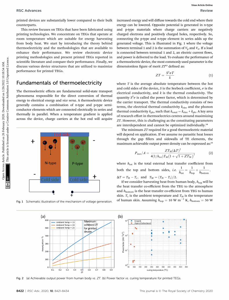
The thermoelectric effects are fundamental solid-state transportphenomena responsible for the direct conversion of thermalenergy to electrical energy and vice versa. A thermoelectric devicegenerally contains a combination of n-type and p-type semi-conductor elements which are connected electrically in series andthermally in parallel. When a temperature gradient is appliedacross the device, charge carriers at the hot end will acquire
Fig. 1 Schematic illustration of the mechanism of voltage generation.
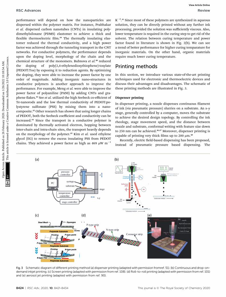
Fig. 2 (a) Achievable output power from human body vs. ZT. (b) Power
8422 | RSC Adv., 2020, 10, 8421–8434
increased energy and will diffuse towards the cold end where theirenergy can be lowered. Opposite potential is generated in n-typeand p-type materials where charge carriers are negativelycharged electrons and positively charged holes, respectively. So,connecting the p-type and n-type element in series adds up thegenerated voltage. This is illustrated in Fig. 1 where the voltagebetween terminal 1 and 2 is the summation of Vp and Vn. If a loadis connected between terminal 1 and 2, an electric current ows,and power is delivered to the load. To evaluate the performance ofa thermoelectric device, themost commonly used parameter is thedimensionless gure of merit ZT13 dened as:
ZT ¼ S2sT
k(1)
where T is the average absolute temperature between the hotand cold sides of the device, S is the Seebeck coefficient, s is theelectrical conductivity, and k is the thermal conductivity. Thequantity S2s is called the power factor, which is determined bythe carrier transport. The thermal conductivity consists of twoterms, the electrical thermal conductivity kelec and the phononthermal conductivity kph, such that ktotal ¼ kelec + kph. A key areaof research effort in thermoelectrics centres aroundmaximizingZT. However, this is challenging as the constituting parametersare interdependent and cannot be optimized individually.14
The minimum ZT required for a good thermoelectric materialwill depend on application. If we assume no parasitic heat lossesthrough the gap llers and sidewalls of TE elements, themaximum achievable output power density can be expressed as:15
Pmax=A ¼ ZTMðDTÞ24ð1=htotÞTM
�1þ ffiffiffiffiffiffiffiffiffiffiffiffiffiffiffiffiffiffiffi
1þ ZTM
p �2 (2)
where htot is the total external heat transfer coefficient from
both the top and bottom sides, i.e.1htot
¼ 1htop
þ 1hbottom
;
DT ¼ TH � Tc; and TM ¼ ðTH � TcÞ=2.If we consider harvesting heat from human body, htop will be
the heat transfer co-efficient from the TEG to the atmosphereand hbottom is the heat transfer co-efficient from TEG to humanskin. Tc is the ambient temperature and TH is the temperatureof human skin. Assuming htop ¼ 10 W m�2 K, hbottom ¼ 50 W
factor vs. curing temperature for printed TEGs.
This journal is © The Royal Society of Chemistry 2020

Review RSC Advances
Ope
n A
cces
s A
rtic
le. P
ublis
hed
on 2
6 Fe
brua
ry 2
020.
Dow
nloa
ded
on 1
/26/
2022
10:
18:5
4 A
M.
Thi
s ar
ticle
is li
cens
ed u
nder
a C
reat
ive
Com
mon
s A
ttrib
utio
n 3.
0 U
npor
ted
Lic
ence
.View Article Online
m�2 K (ref. 16) and Th ¼ 36 �C, Fig. 2(a) shows the relationbetween ZT and maximum output power density achievablewhen harvesting heat from the human body. For this applica-tion, when the ambient temperature is 20 �C, an output powerdensity of 200 mW cm�2 can be achieved with state of the artprinted TEG.
Optimizing thermoelectric materials
Some of the complexity associated with optimizing thecomponents of ZT is discussed here. Electrical conductivity isdened by s ¼ enm, where e is the charge of electrons, n is thecarrier concentration and m is the carrier mobility. Carriermobility can be dened as m ¼ es/m. Here s is mean scatteringtime of the carrier and m is the effective mass. So, conductivitycan be increased by increasing the carrier concentration (n).However, For metal and degenerate semi-conductors, the See-beck coefficient drops with increasing carrier concentration.Consequently, optimization of the carrier concentration iscritical to obtain the best performance. Another importantparameter is the effective charge carrier mass. Higher m isrelated to a at band near the Fermi surface, which increasesthe Seebeck coefficient. However, the higher m will lower thecarrier mobility (m). As mobility is directly proportional toconductivity, lowering carrier mobility will decrease theconductivity. Finally, based on eqn (1), a good thermoelectricmaterial should have high electrical conductivity yet lowthermal conductivity. A direct relationship between electronicthermal conductivity (kelec) and (s) further complicates mate-rials optimization.
There has been signicant research effort focussed on opti-mizing the parameters in eqn (1) to maximize ZT. Apart fromthe well-known thermoelectric material such as Bi2Te3 orSb2Te3, other complex materials including chalcogenides,clathrates, oxides, skutterudites, half-Heusler alloys have beeninvestigated.4 However, most of these materials operate effi-ciently at temperatures much higher than that of the humanbody. Apart from looking for alternate materials, one of themost successful approaches to improve ZT has been to reducethe phonon thermal conductivity without the signicantreduction of the power factor.17,18 This strategy has been ach-ieved via nanostructuring,19,20 embedding nanoparticles intosemiconductors21 or using nanocomposites instead of bulkmaterials.22 The performance improvement is due to the selec-tive scattering of electrons and phonons at interfaces.23 Mahanand Sofo investigated the effect of the transmission function ofcharge carriers on the power factor of thermoelectric materialsand suggested that a delta-like transmission function canimprove the power factor.24 Heremans et al.25 doped PbTe withTl, which introduced resonant energy levels within the valenceband to create sharp delta-like density of states to improve thepower-factor. Another popular method to enhance the Seebeckcoefficient is via energy ltering. By introducing an energybarrier, low energy electrons can be preferentially scatteredwhile high energy electrons are less affected, thereby enhancingthe entropy transport through the material.21 Zebarjadi et al.proposed the modulation doping scheme to enhance the power
This journal is © The Royal Society of Chemistry 2020
factor, where charge carriers are donated from dopants that areconned within the second phase grains to the matrix occu-pying the majority volume.26 Due to the lower scattering in thematrix region void of dopant impurities, the electrical conduc-tivity of the two-phase composite was higher than that of theconventionally doped matrix, resulting in an enhanced powerfactor. Finally, Boukai et al.18 proposed and implemented thepossibility of utilizing the phonon drag effect27–29 to enhance theSeebeck coefficient at low temperatures. Recently it has beenshowed that phonon drag could prevail at a higher temperaturefor lower dimensional materials like silicon nanowires resultingin a very high ZT.18
When it comes to the printing of TE devices, precursormaterials need to be converted to functional inks that areprintable. This adds an extra optimization step for printedTEGs. To date, most of the printed room temperature inorganicTEGs have used Bi2Te3, Sb2Te3 and their alloys. Other inorganicmaterials used in printed TE include Bi2TexSe3�x, Ca3Co4O9 andZnO doped In2O3.30 There are two common approaches toprepare functional inks using these materials. One includes ballmilling the inorganic materials to nanoparticle forms, thendispersing them in aqueous solutions or polymer matrices.Aer printing the ink, a curing step is needed to get rid of thesolvent or polymer. Another method is to use precursors of thefunctional materials as inks. Once printed, a reaction step isneeded on the substrate to convert the precursor to the desiredmaterial. A popular example of this method is the sol–gelprocess to print metal oxides.31 Precursor solution of metal saltsis converted to gel via hydrolysis and printed on a substrate.Post-processing like sintering converts the gel to a thin lm ofmetal oxide. In both methods, the quality of the printed lmdepends on how densely packed the nano-particles are in thenal lm. This is directly related to the curing/sintering step.Typically, the higher the temperature is used for the curing/sintering, the less solvent/polymer remains in the lm. Also,higher temperatures densify the lm. Unfortunately, most ofthe exible substrates used cannot withstand high tempera-tures. So the range of substrate that can be used becomeslimited. This makes the curing temperature another optimiza-tion parameter. Recently, photonic sintering has beenproposed, where UV light is used to sinter the ink withoutadditional heat treatments.32
Apart from the inorganic materials, several organic polymershave been investigated for thermoelectric applications.33–36 Oneadvantage of organic polymers in printing is low curingtemperature.37,38 This enables them to be printed in a widerange of substrates. However, the thermoelectric parameters,conductivity and Seebeck co-efficient, of organic polymers islower than established in-organic materials. Consequently,several unique approaches have been proposed by the researchcommunity to enhance the thermoelectric performance oforganic materials.39–41
Both conducting and non-conducting polymers are utilizedto fabricate thermoelectric devices. Non-conducting polymersare generally used as matrices, where thermoelectric nano-particles are added as the active material. Apart from the ther-moelectric performance of the nanoparticles, the ink
RSC Adv., 2020, 10, 8421–8434 | 8423
RSC Advances Review
Ope
n A
cces
s A
rtic
le. P
ublis
hed
on 2
6 Fe
brua
ry 2
020.
Dow
nloa
ded
on 1
/26/
2022
10:
18:5
4 A
M.
Thi
s ar
ticle
is li
cens
ed u
nder
a C
reat
ive
Com
mon
s A
ttrib
utio
n 3.
0 U
npor
ted
Lic
ence
.View Article Online
performance will depend on how the nanoparticles aredispersed within the polymer matrix. For instance, Prabhakaret al. dispersed carbon nanotubes (CNTs) in insulating poly-dimethylsiloxane (PDMS) elastomer to achieve a thick andexible thermoelectric lm.39 The thermally insulating elas-tomer reduced the thermal conductivity, and a high powerfactor was achieved through the tunneling transport in the CNTnetworks. For conductive polymers, the performance dependsupon the doping level, morphology of the chain and thechemical structure of the monomers. Bubnova et al.40 reducedthe doping of poly(3,4-ethylenedioxythiophene)-tosylate(PEDOT:Tos) by exposing it to reduction agents. By optimizingthe doping, they were able to increase the power factor by oneorder of magnitude. Adding inorganic nano-structures inconductive polymers is another approach to improve theperformance. For example, Meng et al. were able to improve thepower factor of polyaniline (PANI) by adding CNTs and gra-phene akes.42 See et al. utilized the high Seebeck co-efficient ofTe-nanorods and the low thermal conductivity of PEDOT:po-lystyrene sulfonate (PSS) by mixing them into a nano-composite.43 Other research has shown that using longer chainsof PEDOT, both the Seebeck coefficient and conductivity can beincreased.44 Since the transport in a conductive polymer isdominated by thermally activated electron, hopping betweeninter-chain and intra-chain sites, the transport heavily dependson the morphology of the polymer.45 Kim et al. used ethyleneglycol (EG) to remove the excess insulating PSS from PEDOTchains. They achieved a power factor as high as 469 mW m�1
Fig. 3 Schematic diagram of different printingmethod (a) dispenser printdemand inkjet printing. (c) Screen printing (adaptedwith permission fromand (e) aerosol jet printing (adapted with permission from ref. 90).
8424 | RSC Adv., 2020, 10, 8421–8434
K�2.41 Since most of these polymers are synthesized in aqueoussolution, they can be directly printed without any further inkprocessing, provided the solution was sufficiently viscous. Also,lower temperature is required in the curing step to get rid of thesolvent. The relation between curing temperature and powerfactor found in literature is shown in Fig. 2(b). We can seea trend of better performance for higher curing temparature forinorganic materials. On the other hand, organic materialsrequire much lower curing temperature.
Printing methods
In this section, we introduce various state-of-the-art printingtechniques used for electronic and thermoelectric devices anddiscuss their advantages and disadvantages. The schematic ofthese printing methods are illustrated in Fig. 3.
Dispenser printing
In dispenser printing, a nozzle dispenses continuous lamentof ink (via pneumatic pressure) slurries on a substrate. An x–ystage, generally controlled by a computer, moves the substrateto achieve the desired design topology. By controlling the inkrheology, stage movement speed, and the distance betweennozzle and substrate, conformal writing with feature size downto 250 nm can be achieved.46,47 Moreover, dispenser printing iscapable of printing very thick lms up to 200 mm.48
Recently, electric eld-based dispensing has been proposed,instead of pneumatic pressure based dispensing. The
ing (adapted with permission fromref. 51). (b) Continuous and drop-on-ref. 108). (d) Roll-to-roll printing (adaptedwith permission from ref. 101)
This journal is © The Royal Society of Chemistry 2020

Table 1 Dispenser printed TEGs
p-Type n-Type Max temp. (�C) SubstratePerformance(mW m�1 K�2) Ref.
Sb2Te3-epoxy resin composite Bi2Te3-epoxy resin composite 250 Polymide subsrate p-Type: 150 48n-Type: 130
Sb2Te3-epoxy composite Bi2Te3-epoxy composite 350 Glass p-Type: 840 53n-Type: 150
— Mechanical alloyed Bi2Te3 (1% Se) 350 Flex-PCB n-Type: 300 56Bi0.5Sb1.5Te3 with 8 wt%extra Te-epoxy
Bi-epoxy composite 250 — n-Type: 90 59p-Type: 5
— Bi2Te2.7Se0.3 Selective laser melting — n-Type: 1500 58p-Type Bi2Te3 n-Type Bi2Te3 100 PDMS thick lm — 34
Review RSC Advances
Ope
n A
cces
s A
rtic
le. P
ublis
hed
on 2
6 Fe
brua
ry 2
020.
Dow
nloa
ded
on 1
/26/
2022
10:
18:5
4 A
M.
Thi
s ar
ticle
is li
cens
ed u
nder
a C
reat
ive
Com
mon
s A
ttrib
utio
n 3.
0 U
npor
ted
Lic
ence
.View Article Online
electrohydrodynamic (EHD) deposition technique relies onapplying an electric eld to create the force to propel ink fromthe nozzle onto the target substrate. By using high-frequencypulses for the EHD system, a high spatial resolution down to100 nm was achieved.49 Using this technique, researchers haveprinted thin-lm transistors,50 light-emitting diodes,51 mem-ristors,9 articial neural networks10 and QLEDs.52
The main advantage of dispenser printing is low materialwastage and mask free patterning. However, preparing thehighly concentrated and viscous ink is challenging.
One of the rst reported printed TEGs was dispenser printedn-type Bi2Te3 and p-type Sb2Te3.48,53,54 A polymer binder wasused to make pastes, which was then dispenser printed ona polyimide substrate. Due to the lower temperature toleranceof the polyimide substrate, the device was cured at a relativelylow temperature, 250 �C. The device performance was twoorders of magnitude lower than bulk due to the presence ofpolymer binder in the system, which reduces the electricalconductivity. The same group later explored several techniquesto improve the performance, including mechanical alloying andSe and Te doping.55,56 They also integrated their dispenserprinted devices with disperser printed micro-batteries demon-strating a complete power supply for a wearable sensornetwork.57 Wu et al. combined selective laser melting (SLM)with dispenser printing to achieve device performance compa-rable to bulk manufacturing technique.58 However, using SLMcomplicates the fabrication process signicantly. The dispenserprinting method was also utilized to fabricated cross-planeTEGs. Jo et al. utilized thick PDMS lm with holes as mold.34
p-Type and n-type Bi2Te3 mixed with a polymer binder, wasdispenser printed to ll up the holes. The device was annealedat 100 �C. Their 50 � 50 mm device was able to generate 2.1 mWpower at a 19 K temperature difference (Table 1).
Inkjet printing
Inkjet printing is a derivative of dispenser printing where inkdrops exit the nozzle by a dynamic process. Inkjet printing isgenerally categorized into the continuous inkjet and the drop-on-demand (DoD) method. Due to its material relevance forthermoelectric device fabrication, we will primarily focus onDoD printing. By controlling the contraction expansion of thepiezoelectric actuator, individual ink droplets can be jetted out
This journal is © The Royal Society of Chemistry 2020
from the nozzle forming the desired pattern on the substrate.The printed pattern can be easily modied by changing thedigital le that controls the actuator. The printability dependson the nozzle radius and viscosity, density and surface tensionof the ink.60
Inkjet printing has been intensely investigated as a low costfabrication technique for the electronics industry. Chen et al.have demonstrated fully inkjet-printed transistors with mobilityof approximately 1 cm2 V�1 s�1 and an on-to-off ratio of �107.6
Liu et al. demonstrated inkjet printed QLEDs reaching themaximum luminance of 89 500 cd cm�2.61 Furthermore,researchers have investigated the viability of inkjet-printedimage sensors.62
In spite of the wide application, commercial products usinginkjet printed materials are not currently widely available. Thiscan be attributed to the following: (1) when the size of theparticles contained in ink is in the order of nozzle diameter, theprinter nozzle gets easily clogged, affecting the printing pattern.Since printing resolution depends on the nozzle size, usinga larger nozzle to avoiding clogging affects the achievableresolution. (2) Droplets form a ‘coffee ring’ on the substratecaused by non-uniform drying of the ink. The centre of thecoffee ring is thinner than the edge leading to non-uniformityand undesirable device characteristics. There have beenseveral efforts to minimize non-uniform printing, includingelectrowetting,63 eddies,64 and particle trapping.65 However,these methods have not been thoroughly investigated in thecontext of ink-jet printing.
Inkjet printing is another highly used method to printthermoelectric devices (Table 2). Since the lms are thin, mostof the inkjet printed TEGs are planar device. Both inorganic,polymer and carbon based materials have been printed usingink-jet printed techniques. One of the rst reported inkjetprinted inorganic TEGs were fabricated using p-type Sb1.5Bi0.5-Te3 nanoparticles and n-type Bi2Te2.7Se0.3 nanoparticles basedinks.66 Commercial stabilizer was used to formulate aqueoussolutions of the nanoparticles and aco-solvent was used toachieve the viscosity and surface tension suitable for inkjetprinting. The Ag nanoparticle-based electrodes were also inkjetprintedmaking the device fully printed. The group was also ableto print the TEGs on exible polyamide substrate. They couldachieve a power factor of 77 mW m�1 K�2 for n-type and 183 mW
RSC Adv., 2020, 10, 8421–8434 | 8425

Table 2 List of inkjet printed TEGs
p-Type n-Type Max temp. Substrate Performance (mW m�1 K�2) Ref.
Sb1.5Bi0.5Te3 Bi2Te2.7Se0.3 400 �C Glass/polymide p-Type: 183 66n-Type: 77
Bi2Te3 nanowires 400 �C Glass n-Type: 163 67(Bi0.5Sb1.5Te3) nanowires (Bi2Te3) nanowires 450 �C Polymide p-Type: 180 68
n-Type: 110(PEDOT:PSS-ink), ZnO-ink — 150 �C Glass — 70PAA doped carbon nanotube (CNT) PEI doped carbon nanotube (CNT) 85 �C Flexible cable p-Type: 129 37
n-Type: 135PEDOT:PSS (PEDOT)xV2O5 100 �C Photo-paper p-Type: 17.12 38
n-Type: 2.0PEDOT:Tos — 110 �C Silicon substrate p-Type: 324 40(Poly[Cux(Cu-ett)])/PVDF Poly[Kx(Ni-ett)]/PVDF 90 �C PET p-Type: 1.92 71
n-Type: 1.58
RSC Advances Review
Ope
n A
cces
s A
rtic
le. P
ublis
hed
on 2
6 Fe
brua
ry 2
020.
Dow
nloa
ded
on 1
/26/
2022
10:
18:5
4 A
M.
Thi
s ar
ticle
is li
cens
ed u
nder
a C
reat
ive
Com
mon
s A
ttrib
utio
n 3.
0 U
npor
ted
Lic
ence
.View Article Online
m�1 K�2 for p-type materials. Unfortunately, the processrequires a high annealing temperature of 400 �C, necessary todecompose the polymeric stabilizer making it unsuitable formany exible substrates.
Chen et al. was able to improve the performance of n-typematerial utilizing nano-structuring effect. Their Bi2Te3 nano-wires based n-type ink could achieve a power factor of 163 mWm�1 K�2 at room temperature.67 The same group recently usednanowires for both n-type and p-type material as well asprinting them on exible polymide substrates.68 Their n-typeand p-type ink consisted of BiTe and Bi0.5Sb1.5Te3 nanowiresand a eutectic gallium–indium (EGaIn) liquid metal as theelectrode. Even though they did not use any stabilizer, a highannealing temperature of 450 �C was required to sinter the ink.
One solution to high annealing temperature is to usepolymer-based organic thermoelectric material. By controllingthe oxidation of PEDOT:Tos, Bubnova et al. were able to achievemuch higher power factor compared to many printed inorganicTEGs using annealing temperature of only 110 �C.69 SincePEDOT:Tos in not soluble, a solution of EDOT monomer andoxidant (Fe(Tos)3) were inkjet printed on a warm Ag electrode tofacilitate in situ polymerization to fabricate the TE leg. Otherreports on PEDOT based inkjet printed device include mixingwith inorganic nanoparticles. Besganz et al. mixed ZnO nano-particle with PEDOT:PSS-ink and varied its concentration.70 Theresults showed mixing 20% ZnO improves the performancecompared to pure PEDOT:PSS, but adding more ZnO degradesthe performance. A lower annealing temperature of 150 �C wasalso used, which might be too low for the activation of ZnO.
Most of the conductive polymers are p-type material. To thisend, Ferhat et al. inkjet printed composite of PEDOT and V2O5,5H2O gel that performed as the n-type component of the TEG.38
Detergent additives (Triton X-100) were used to control theviscosity of the ink. PEDOT:PSS, (PEDOT)xV2O5 and silver inkwas printed on photo paper to constitute the n-type leg, p-typeleg and electrodes. Because the device was all polymer based,an annealing temperature of 100 �C was sufficient to cure thedevice. Here, the power factor of the n-type leg was two orders ofmagnitude lower compared to other printed inorganic mate-rials. Moreover, the PEDOT:PSS was not optimized resulting insignicantly lower power factor for p-type leg.
8426 | RSC Adv., 2020, 10, 8421–8434
On a different front, carbon-based inks showed promisingperformance as inkjet printed devices. Park et al. used CNT asboth p-type and n-type legs by doping with PAA and PEIrespectively.37 They controlled the doping to obtain optimalcarrier concentration and achieved power factor of 129 and 135for p-type and n-type legs. This is comparable to inkjet printedinorganic device making them a promising candidate for fullyprinted TEGs. The annealing temperature of the ink was 85 �Ceven though the electrodes were cured at 120 �C.
Jiao et al. inkjet printed insoluble and infusible metal coor-dination polymers.71 Both n (poly[Kx(Ni-ett)]/PVDF)- and p-type(poly[Cux(Cu-ett)]/PVDF) composites were obtained by ball-milling. The composite material maintained the performanceof bulk reaching PF of 1.92 and 1.58 mWm�1 K�2 at 400 K for n-and p-type composite respectively.
Screen printing
Screen printing is a popular technique that has been widelyused in commercial printing processes. Recently, this techniquehas found popularity in electronics applications.72 Typically,stencils or patternedmesh are used as the template. Viscous inkis forced through the mesh using a squeegee type device. Thedeposition resolution and thickness of the pattern depends onthe viscosity of the ink used and the density of the mesh. A 100mm thick layer with a 100 mm resolution can be achieved with anink viscosity of 50 pascal.73 Researchers have demonstratedmass production capabilities of photovoltaic cells,74 RFantennas75 and light emitting diodes76 using the screen printingmethod.
The advantage of screen printing, as compared to otherprinting methods, include the broader range of availablesubstrates and inks that are compatible with this method. Thedisadvantage of this method includes high viscosity require-ment of the ink and the relative longer drying time. Moreover,the screen printed lm is known to have a rough surface and aresusceptible to cracking and delamination.74,77
Screen printing is one of the most popular methods used toprint thermoelectric devices (Table 3). Both organic and inor-ganic inks has been used in conjunction with this method. Therst reported screen printed TEG contained p-type Sb and n-type Bi0.85Sb0.15.78 The authors investigated different binders
This journal is © The Royal Society of Chemistry 2020

Table 3 Screen printed TEGs
p-Type n-Type Max temp. Substrate Performance (mW m�1 K�2) Ref.
Sb Bi0.85Sb0.15 — Kapton p-Type: 10 78n-Type: 90
Bi0.5Sb1.5Te3 Bi2Sb0.3Te2.7 250 �C Al2O3 p-Type: 10 79n-Type: 50
Bi2Te3 500 �C SiO2/Si n-Type: 30 82ZnSb CoSb3 500 �C p-Type: 370 85
n-Type: 50Sb2Te3 Bi3.2Sb1.8 250 �C Kapton p-Type: 215 84
n-Type: 141Silver Nickel 350 �C PolyimidePEDOT:PSS + 5% ethylene glycol — 70 �C Paper p-Type: 25 87CNT–polystyrene composite — — Polyethylene naphthalate lm p-Type: 0.15 88Ca3Co4O9 (ZnO)5In2O3 1400 �C Alumina p-Type: 1.6 30
n-Type: 1.4Sb2Te3 Bi2Te3 530 �C Glass fabric p-Type: 1200 86
n-Type: 1175
Table 4 Aerosol jet/spray printed TEGs
p-Type n-Type Max temp. SubstratePerformance(mW m�1 K�2) Ref.
H2SO4 treated tellurium-PEDOT:PSShybrid composite
120 �C Glass or exible polyimide p-Type: 284 92
CNT doped P3HT Polymide p-Type: 325 93Sb2Te3 + MWCNT + PEDOT:PSS p-Type: 41 94BiTe2.7Se0.3 nanoplate Photonic sinteritng p-Type: 730 95
Review RSC Advances
Ope
n A
cces
s A
rtic
le. P
ublis
hed
on 2
6 Fe
brua
ry 2
020.
Dow
nloa
ded
on 1
/26/
2022
10:
18:5
4 A
M.
Thi
s ar
ticle
is li
cens
ed u
nder
a C
reat
ive
Com
mon
s A
ttrib
utio
n 3.
0 U
npor
ted
Lic
ence
.View Article Online
including ethylene glycol, 2-component epoxy glue and PMMA,and could achieve a power factor of 90 mWK�2 m�1. Kapton tapewas used as the substrate and were able to coil up the devices,demonstrating their mechanical exibility. However, none ofthe curing conditions were described. Research effort79–85 hasimproved the performance of BiTe and BiSb based TEGs andlowered the curing temperature by optimizing the ink, usingsuitable binder additive, mechanical alloying, and doping.Curing temperature as low as 250 �C has been able to achievepower factors of 215 mW m�1 K�2 and 141 mW m�1 K�2 for p-type Sb2Te3 and n-type Bi3.2Sb1.8.84 Kim et al. proposed a novelsubstrate-less TEG by screen printing Bi2Te3 and Sb2Te3 pasteon glass fabric.86 Since this method does not use any substrate,a high curing temperature of 530 �C was used. As a result theycould achieve higher power factors of 1066 mW m�1 K�2 for n-type and 1166 mW m�1 K�2 for p-type material.
Apart from BiTe and BiSb based TEGs, Rudez et al. screenprinted Ca3Co4O9 as p-type leg and a (ZnO)5In2O3 as n-type legto print TEGs on alumina substrate.30 They also screen printedthe electrodes making it a fully printed TEG device. However,because of the ink formulation, the process required very hightemperatures of up to 1400 �C.
Similar to other printing techniques, by using organic andcarbon-based material lower curing temperature can be ach-ieved. Wei et al. demonstrated screen printing process to printPEDOT:PSS on paper.87 Their inks consisted of aqueousPEDOT:PSS with 5% ethylene glycol. Their curing temperature
This journal is © The Royal Society of Chemistry 2020
was 150 �C. Their paper substrate was thermally stablecompared to other polymer based substrate approaches.Moreover, their aqueous solution had better wettability onpaper substrates. Suemori et al. used ink composed of CNT anddissolved polystyrene in 1,2-dichlorobenzene to screen print onpolyethylene naphthalate substrate.88 However, the process isnot fully printable since vacuum deposition was used to formthe electrodes.
Aerosol jet and spray printing
Aerosol jet printing is another popular method for printableelectronics. In this method, an atomizer aerosolizes the ink intoliquid particles of size ranging from 20 nm to 5 mm. Inert gas orcompressed airow is used to transfer the ink particle to thesubstrate. Several electronic devices, including thin lm tran-sistor displays89 and solar cells,90 have been printed usingaerosol jet/spray printing.
The main advantage of spray printing is the higher allowabledistance between print head and substrate making it possible toprint on non-at and non-smooth substrates. The achievableresolution is higher than inkjet printing.91 However, edgesharpness in lower and localized crystallization caused by thesheath gas can detrimentally affect the bonding layer quality(Table 4).
Canlin et al.94 used an aerosol-jet printing technique tofabricate TEG on exible substrates. The unique ink consistedof well-dispersed high-S Sb2Te3 nanoakes, high-conductive
RSC Adv., 2020, 10, 8421–8434 | 8427
Table 5 Brush painted and roll-to-roll printed TEGs
p-Type n-Type Max temp. SubstratePerformance(mW m�1 K�2) Ref.
Brush paint BiSbTe Sb2Te3-basedchalcogenidometalate(ChaM) for n-type BiTeSe
— Polyimide — 98
— Bi2Te2.7Se0.3 400 �C — 99Roll-to-roll PEDOT:PSS 140 �C PET foil — 100
PEDOT:PSS n-Doped graphene Plasma treated plastic — 101SWCNT/PEDOT:PSS SWCNT/PVP Infrared heating Polyimide p-Type: 0.02 102
n-Type: 0.24
RSC Advances Review
Ope
n A
cces
s A
rtic
le. P
ublis
hed
on 2
6 Fe
brua
ry 2
020.
Dow
nloa
ded
on 1
/26/
2022
10:
18:5
4 A
M.
Thi
s ar
ticle
is li
cens
ed u
nder
a C
reat
ive
Com
mon
s A
ttrib
utio
n 3.
0 U
npor
ted
Lic
ence
.View Article Online
multi-walled carbon nanotubes (MWCNTs) and PEDOT:PSS.Using optimal composition and surface treatment, powerfactors of �41 mW m�1 K�2, were achieved. Recently, Mortazaet al.95 achieved a record high power factor of 730 mW m�1 K�2
for Bi2Te2.7Se0.3 nanoplate based inks using a combination ofaerosol jet printing and photonic sintering. Cheon et al. usedspray painting techniques to print the nanocomposite of CNTand P3HT.93 They used a nozzle diameter of 200 mm and
Table 6 Comparison among different printing methods
Method Details Speed
Dispenser printing -Stage needs to be movedbased on the pattern
Slow
-Mask free method
-Needs preussre or electriceld for ink dispension
Inkjet printing -Mask free method Slow
-Nozzle moves based onpattern-Non-contact printing,protects substrate fromcontamination or damage
Screen printing -Stencil or mesh needed asmask
Moderate
-A squeegee type device isused to force ink through themesh
Roll-to-roll printing -Stencil or mesh needed asmask
Fast
-A rotary structure needed tomove the substrate-Hard contact compressionis used to transfer the ink tothe substrate
Aerosol jet printing -Compressed air owrequired
Slow
-Non-contact printing,protects substrate fromcontamination or damage-Larger nozzle size cantolerate larger ink particles
Brush painting -Stencil/mask needed Slow
-Cheapmethod, brush needsto be moved manually ovarthe stencil
8428 | RSC Adv., 2020, 10, 8421–8434
polyamide was used as the substrate. The p-type composite wasable to produce a power factor of 325 � 101 mW m�1 K�2. Baseet al. treated tellurium-PEDOT:PSS composite with H2SO4 andspray printed them. By optimizing the H2SO4 treatment, theyachieved a power factor of 284 mW m�1 K�2. Till now, only p-type material has been aereosol jet printed, leaving room forfurther research on n-type material.
Ink compatibility Printed structure
-Compatible for bothorganic and inorganic inks
-Only prints on at surface
-Larger particle size canblock nozzle
-Multiple run needed toprint vertical structure-Small feature size can beachieved
-Compatible for bothorganic and inorganic inks
-Only prints on at surface
-Larger particle size canblock nozzle
-Printing vertical structurenot possible
-Low viscosity low volatility -Small feature size can beachieved
-Highly viscous ink needed -Can print on non-atsurface
-No limitation about particlesize
-Can print thick lm-Small feature size cannot beachieved
-Medium to highly viscousink needed
-Can print on exible surface
-No limitation about particlesize
-Printing layers on top ofeach other is difficult due toalignment issues
-Inks needs to be volatile Can print on non-atsubstrate
-High viscous ink needed -Can print on non-atsubstrate-Small feature size cannot beachieved-Can print thick lm
This journal is © The Royal Society of Chemistry 2020

Review RSC Advances
Ope
n A
cces
s A
rtic
le. P
ublis
hed
on 2
6 Fe
brua
ry 2
020.
Dow
nloa
ded
on 1
/26/
2022
10:
18:5
4 A
M.
Thi
s ar
ticle
is li
cens
ed u
nder
a C
reat
ive
Com
mon
s A
ttrib
utio
n 3.
0 U
npor
ted
Lic
ence
.View Article Online
Roll-to-roll printing
Roll-to-roll printing is similar to the screen printing technique,where a rotary screen is used for continuous processing of theweb (substrate). Hard contact compression is used to transferthe ink to the substrate. This is a high resolution and highthroughput process and has been widely used to fabricate bothactive and passive electronic devices.96 Dilfer et al. demon-strated a fully R2R printed metal oxide thin lm transistor.97
Moreover, R2R printing has been used to fabricate solar cells8
and light emitting diode.7
The main advantage of R2R printing is the high throughput,making it the most lucrative printing technique for high volumeproduction. However, making a multilayer device ischallenging.
Even though roll to roll printing method is becomingincreasingly popular for applications like solar cell, and transis-tors, it is not yet widely investigated for TEGs (Table 5).Søndergaard et al. used PEDOT:PSS and silver ink to print 18 000serially connected TEG legs.100 The printing was undertaken onPET foil in a three step process that included printing the bottomelectrode, PEDOT:PSS and the top electrode. They achieveda speed of 300 junctions per minute, demonstrating mass pro-ducibility of these TEGs. However, the measured Seebeck co-efficient of their devices was much lower than other reportedvalues. This difference can be attributed to the their unoptimizedPEDOT:PSS solution.
Zhang et al. used roll to roll printing to print both p-type andn-type legs.101 PEDOT:PSS mixed with DMSO was used as the p-type ink and n-doped graphene was used as the n-type ink. Theyused three sequential rollers to transfer the complete patternsimultaneously. Their printing speed was 15–20 mm min�1.Their research monograph did not characterize the perfor-mance of individual legs of the TEGs but reported an overalloutput power of 0.24 mW m�2 at a temperature of 10 �C. Singlewall carbon nanotubes were also used as inks in roll-to-rollprinting.102 They used infrared heating to sinter the ink. Inthis process only the inks can be selectively heated withoutheating up the substrate. This method can enable the usage ofsubstrates that cannot withstand high temperature sintering.
To our knowledge, no inorganic material has been used inroll-to-roll printed TEGs. Moreover, the performance in the roll-to-roll printed TEGs are signicantly lower than TEGs reportedby other printing technique using the same material. Thisopens up a signicant research opportunity in this eld.
Brush printing
Brush painting is a simple and cheap method which requiresa template and brush to print pattern on a substrate.99 Thethickness of the lm depends on parameters such as theviscosity of the ink and the brush speed. This method isdesirable for proof of concept experiments since it doesn'trequire expensive equipment or setup, but it is limited by lowresolution and speed. Moreover, a template is required whichrequires an extra fabrication step.
Park et al. proposed brush printing to print on surface of anygeometrical shape.98 Their brush printing method utilized
This journal is © The Royal Society of Chemistry 2020
Bi2Te3 based organic ink which used Sb2Te3 chalcogenidome-talate as a sintering aid. Using this printing method, theresearchers were able to print directly on hemisphere surface.Another reported TEG using brush printing method utilizedcustom designed Bi2Te2.7Se0.3 based ink. The lms were 100–150 mm thick making the device suitable for through planedevice (Table 6).99
Device and application
In this section, we present different structures of TEGs and theirproposed application. The main design challenge in a TEG is tomaximize the temperature difference across the junctions.Keeping this in mind, we have categorized TEGs into twogroups: (1) planar TEGs where the junctions are on the sameplane as the substrate and (2) through-plane TEGs where thejunctions are in the cross-plane direction of the substrate. Inmost of the heat sources, like the human body or a hot pipe, thesurface remains at the same temperature. So, to createa temperature difference across planar devices, researchershave proposed innovative device designs such as corrugation,origami, z-scheme folding and vertical staking.103–106 Here wefocus on techniques that have been implemented usingprinting methods.
One solution to create temperature difference across planardevice is to put the device vertically on the hot surface. Iezziet al. placed planar TEGs vertically on a hot plate. The TEGswere able to power a RFduino and send temperature reading toa cell phone.107 Qingshuo et al. printed planar thermocouple onpaper, then stacked up to 300 pieces of papers, and used themvertically between the hot and cold surface87 (Fig. 4(a)). Thestacked papers were connected via copper sheet or wires. As theoutput voltage was low, a step up converter was used. Fora 100 �C temperature difference, this device generated enoughenergy to power an LED. The group later rened their methodusing thermal lamination to achieve an output power of 24 mWcm�2 at 50 �C temperature difference.108 Wang et al. proposeda similar approach of stacking planar TEG.57 Using 250 ther-mocouples, they could generate 203.5 mW of power at 20 �Ctemperature difference. They used both the planes of thesubstrate (Fig. 4(b)). Thermoelectric elements were printed onthe top layer, and connectors were printed on the bottom layerwhile through hole vias were used to connect between thelayers. The group also printed micro-batteries and used theTEGs to charge them. Another reported approach is to organizethe TE element radially, keeping the heat source at centre. Yuanet al. screen printed BiTe based TE legs radially and useda radio-isotope at the centre to create temperature difference.109
Madan et al. also proposed radially oriented planar TEGs, asshown in Fig. 4(d). A power density of 1230 mW cm�2 at 70 K wasachieved from the radial TEG.54 Menon et al. used a mixture ofradial arrangement and stacking.110 However, they could onlyreach 15 nW cm�2 at 45 K temperature difference mainly due tothe low-efficiency material used. Another popular technique toutilize planar TEG is to coil them up.78 Cao et al. used theirscreen-printed TEG to coil up into a cylinder.111 Their outputpower was 12.7 nW cm�2 for 20 �C temperature difference. It
RSC Adv., 2020, 10, 8421–8434 | 8429
Table 7 Performance comparison of different orientation of planar TEGs
Orientation Printing method Material Output (mW cm�2) Ref.
Vertical stacking Screen printing PEDOT:PSS 24, DT ¼ 50 K 108Vertical stacking Dispenser printing Bi2Te3 and Sb2Te3 57Radial arrangement Dispenser printing Bi and Bi0.5Sb1.5Te3 1230, DT ¼ 70 K 54Radial arrangement Screen printing BiTe 109Radial arrangement + stacking Brush painting Polymer based 0.015, DT ¼ 45 K 110Coil up Screen printing BiTe/SbTe 0.012, DT ¼ 20 K 111Folded structure Dispenser printing Polymer-based 0.001, DT ¼ 10 K 92
Fig. 4 Device made from planar TEG (a) schematic illustration of planar TEG stacked vertically (adapted with permission form ref. 87). (b)Dispenser printed vertically stacked planar TEG on flexible substrate (adapted with permission from ref. 55). (c) Schematic illustration of thefolded structure proposesd in ref. 91. (d) Radially oriented planar TEG (adapted with permission from ref. 52).
RSC Advances Review
Ope
n A
cces
s A
rtic
le. P
ublis
hed
on 2
6 Fe
brua
ry 2
020.
Dow
nloa
ded
on 1
/26/
2022
10:
18:5
4 A
M.
Thi
s ar
ticle
is li
cens
ed u
nder
a C
reat
ive
Com
mon
s A
ttrib
utio
n 3.
0 U
npor
ted
Lic
ence
.View Article Online
should be noted that the inside of the cylinder was hollow,which reduced the output power density. Bending radius is animportant factor for coiled up TEGs that will dictate how closelythe thermocouples can be packed.111 Bae et al. proposed anothernovel structure of folding their TEGs, which are dispenserprinted on exible substrate as shown schematically in Fig.4(c).92 They could achieve an output power of 1 nW cm�2 fora temperature difference of 10 �C (Table 7).
In through-plane TEGs thermoelectric elements are grownvertically to the plane of the substrate. They generally consist oftwo planes, where temperature difference can be applied. All theconventional TEGs are through-plane devices. However,printing through plane devices is challenging since most of theprinting technique prints very thin lms.
Jo et al. used a PMMA mould to make holes in PDMS thicklm and dispenser printed TE inks in the holes34 (Fig. 5(a)). Thethickness of the device was 4 mm. PDMS was chosen due to itsdesireable properties of exibility and electrically and thermally
8430 | RSC Adv., 2020, 10, 8421–8434
insulating behavior. Their device was able to generate 84 nWcm�2 at 19 �C temperature difference. Recently, Zhang et al.were able to print through-plane 3-D TEGs using roll to rollprinting.102 Their device reached an output power density of1.49 mW m�2 at 25 �C temperature difference. They alsodemonstrated an integrated body heat harvester that can poweran LED. A coin-sized supercapacitor was used to boost thegenerated voltage. Kim et al. used extrusion based printing to 3-D print through-plane TEGs.112 The method was capable ofprinting TEGs on any geometries. They demonstrated a real-world application by 3-D printing half ring TEGs of analumina pipe (Fig. 5(c)). The device achieved an output powerdensity of 1.42 mW cm�2 at a temperature difference of 39 �C.Another innovative technique is to use fabric as the printingsubstrate. The ink ltrates through the fabric via capillary effectwhilst the fabric acts as a support structure. So, no externalsubstrate is needed. Kim et al. screen printed such TEGs onglass fabric.86 Their device reached 3.5 mW cm�2 for 50 �C
This journal is © The Royal Society of Chemistry 2020

Fig. 5 Through plane TEGs (a) through plane TEG embedded in PDMS substrate (adapted with permission from ref. 34). (b) Band-aid stylethrough plane TEG (adapted with permission from ref. 86). (c) Schematic illustration of the process of 3-d printing TEG on hot pipe (adapted withpermission from ref. 111). (d) Schematic illustration of screen printed CNT based TEG (adapted with permission from ref. 88).
Review RSC Advances
Ope
n A
cces
s A
rtic
le. P
ublis
hed
on 2
6 Fe
brua
ry 2
020.
Dow
nloa
ded
on 1
/26/
2022
10:
18:5
4 A
M.
Thi
s ar
ticle
is li
cens
ed u
nder
a C
reat
ive
Com
mon
s A
ttrib
utio
n 3.
0 U
npor
ted
Lic
ence
.View Article Online
temperature difference (Fig. 5(b)). Soumeri et al. used CNT–polystyrene composite to fabricate exible and lightweight TEGas shown in Fig. 5(d) achieving output power of 55 mW m�2 at70 �C temperature difference.88
Conclusions
The eld of thermoelectricity relies on optimizing the parame-ters that have opposing performance effects. Printing thesethermoelectric materials involves further optimization of theink and printing techniques. Researchers have investigatedvarious thermoelectric materials, substrates and methods withthe aim of increase the efficiency of the TEGs. Notwithstandingthe excellent progress, there remains signicant room to furtherimprove performance and optimise inks, especially those basedon organic materials. In terms of inorganic material, the key toimprove performance will be to develop inks that require lowercuring temperature. With the increasing demand for wearableelectronics and the great promise for TEGs to power them, thereis signicant scope for improvements in this exciting researcheld.
This journal is © The Royal Society of Chemistry 2020
Conflicts of interest
There are no conicts to declare.
Acknowledgements
The authors acknowledge the support from the Australianresearch Council under Linkage Scheme with the grant ARCResearch Hub for Graphene Enabled Industry Transformation,funding under Industrial Transformation Research HubIH150100003. J.-H. Bahk is thankful for the nancial supportfrom NSF under Grant DMR-1905571.
References
1 A. Vassighi andM. Sachdev, Thermal and power managementof integrated circuits, Springer Science & Business Media,2006.
2 J. R. Lim, J. F. Whitacre, J. P. Fleurial, C. K. Huang,M. A. Ryan and N. V. Myung, Adv. Mater., 2005, 17(12),1488–1492.
RSC Adv., 2020, 10, 8421–8434 | 8431

RSC Advances Review
Ope
n A
cces
s A
rtic
le. P
ublis
hed
on 2
6 Fe
brua
ry 2
020.
Dow
nloa
ded
on 1
/26/
2022
10:
18:5
4 A
M.
Thi
s ar
ticle
is li
cens
ed u
nder
a C
reat
ive
Com
mon
s A
ttrib
utio
n 3.
0 U
npor
ted
Lic
ence
.View Article Online
3 Q. Zhang, Y. Sun, W. Xu and D. Zhu, Adv. Mater., 2014,26(40), 6829–6851.
4 S. LeBlanc, S. K. Yee, M. L. Scullin, C. Dames andK. E. Goodson, Renewable Sustainable Energy Rev., 2014,32, 313–327.
5 P. C. Joshi, R. R. Dehoff, C. E. Duty, W. H. Peter, R. D. Ott,L. J. Love and C. A. Blue, in Direct digital additivemanufacturing technologies: Path towards hybrid integration,2012 Future of Instrumentation International Workshop(FIIW) Proceedings, IEEE, 2012, pp. 1–4.
6 P. Chen, Y. Fu, R. Aminirad, C. Wang, J. Zhang, K. Wang,K. Galatsis and C. Zhou,Nano Lett., 2011, 11(12), 5301–5308.
7 A. Sandstrom, H. F. Dam, F. C. Krebs and L. Edman, Nat.Commun., 2012, 3, 1002.
8 R. Søndergaard, M. Hosel, D. Angmo, T. T. Larsen-Olsenand F. C. Krebs, Mater. Today, 2012, 15(1–2), 36–49.
9 J. Yong, B. Hassan, Y. Liang, K. Ganesan, R. Rajasekharan,R. Evans, G. Egan, O. Kavehei, J. Li and G. Chana, Sci. Rep.,2017, 7(1), 14731.
10 J. Yong, Y. Liang, Y. Yu, B. Hassan, S. Hossain, K. Ganesan,R. R. Unnithan, R. Evans, G. Egan and G. Chana, ACS Appl.Mater. Interfaces, 2019, 17521–17530.
11 S. Khan, L. Lorenzelli and R. S. Dahiya, IEEE Sens. J., 2014,15(6), 3164–3185.
12 D. R. Gamota, P. Brazis, K. Kalyanasundaram and J. Zhang,Printed organic and molecular electronics, Springer Science &Business Media, 2013.
13 G. D. Mahan, APL Mater., 2016, 4(10), 104806.14 D. M. Rowe, CRC Handbook of Thermoelectrics, CRC Press,
1995.15 C. Goupil, Continuum theory and modeling of thermoelectric
elements, John Wiley & Sons, 2015.16 J.-H. Bahk, H. Fang, K. Yazawa and A. Shakouri, J. Mater.
Chem. C, 2015, 3(40), 10362–10374.17 R. Venkatasubramanian, E. Siivola, T. Colpitts and
B. O'Quinn, Nature, 2001, 413(6856), 597–602.18 A. I. Boukai, Y. Bunimovich, T.-K. Jamil, Y. Jen-Kan,
W. A. Goddard Iii and J. R. Heath, Nature, 2008,451(7175), 168–171.
19 M. Sharafat Hossain, F. Al-Dirini, F. M. Hossain andE. Skadas, Sci. Rep., 2015, 5, 11297.
20 M. S. Hossain, D. H. Huynh, L. Jiang, S. Rahman,P. D. Nguyen, F. Al-Dirini, F. Hossain, J.-H. Bahk andE. Skadas, Nanoscale, 2018, 10(10), 4786–4792.
21 W. Kim, J. Zide, A. Gossard, D. Klenov, S. Stemmer,A. Shakouri and A. Majumdar, Phys. Rev. Lett., 2006, 96(4),045901.
22 A. F. May, J.-P. Fleurial and G. Snyder, Phys. Rev. B: Condens.Matter Mater. Phys., 2008, 78(12), 125205.
23 D. M. Rowe, Thermoelectrics handbook: macro to nano, CRCpress, 2018.
24 G. D. Mahan and J. O. Sofo, Proc. Natl. Acad. Sci. U. S. A.,1996, 93(15), 7436–7439.
25 J. P. Heremans, V. Jovovic, E. S. Toberer, A. Saramat,K. Kurosaki, A. Charoenphakdee, S. Yamanaka andG. Snyder, Science, 2008, 321(5888), 554–557.
8432 | RSC Adv., 2020, 10, 8421–8434
26 M. Zebarjadi, G. Joshi, G. Zhu, B. Yu, A. Minnich, Y. Lan,X. Wang, M. Dresselhaus, Z. Ren and G. Chen, Nano Lett.,2011, 11(6), 2225–2230.
27 H. J. Goldsmid, Thermoelectric refrigeration, Plenum Press,1964.
28 C. Herring, Phys. Rev., 1954, 96(5), 1163–1187.29 D. Emin, Effects of Charge Carriers'Interactions on Seebeck
Coefficients, in Thermoelectrics Handbook, CRC Press, 2005,p. 5.
30 R. Rudez, P. Markowski, M. Presecnik, M. Kosir, A. Dziedzicand S. Bernik, Ceram. Int., 2015, 41(10), 13201–13209.
31 R. Sui and P. Charpentier, Chem. Rev., 2012, 112(6), 3057–3082.
32 R. Danaei, T. Varghese, M. Ahmadzadeh, J. McCloy,C. Hollar, M. Sadeq Saleh, J. Park, Y. Zhang and R. Panat,Adv. Eng. Mater., 2019, 21(1), 1800800.
33 J. L. Blackburn, A. J. Ferguson, C. Cho and J. C. Grunlan,Adv. Mater., 2018, 30(11), 1704386.
34 S. Jo, M. Kim, M. Kim and Y.-J. Kim, Electron. Lett., 2012,48(16), 1015–1017.
35 M. He, F. Qiu and Z. Lin, Energy Environ. Sci., 2013, 6(5),1352–1361.
36 G. Chen, W. Xu and D. Zhu, J. Mater. Chem. C, 2017, 5(18),4350–4360.
37 K. T. Park, J. Choi, B. Lee, Y. Ko, K. Jo, Y. M. Lee, J. A. Lim,C. R. Park and H. Kim, J. Mater. Chem. A, 2018, 6(40), 19727–19734.
38 S. Ferhat, C. Domain, J. Vidal, D. Noel, B. Ratier andB. Lucas, Sustainable Energy Fuels, 2018, 2(1), 199–208.
39 R. Prabhakar, M. S. Hossain, W. Zheng, P. K. Athikam,Y. Zhang, Y.-Y. Hsieh, E. Skadas, Y. Wu, V. Shanov andJ.-H. Bahk, ACS Appl. Energy Mater., 2019, 2(4), 2419–2426.
40 O. Bubnova, Z. U. Khan, A. Malti, S. Braun, M. Fahlman,M. Berggren and X. Crispin, Nat. Mater., 2011, 10(6), 429.
41 G. H. Kim, L. Shao, K. Zhang and K. P. Pipe, Nat. Mater.,2013, 12(8), 719.
42 C. Meng, C. Liu and S. Fan, Adv. Mater., 2010, 22(4), 535–539.
43 K. C. See, J. P. Feser, C. E. Chen, A. Majumdar, J. J. Urbanand R. A. Segalman, Nano Lett., 2010, 10(11), 4664–4667.
44 Z. Fan, D. Du, H. Yao and J. Ouyang, ACS Appl. Mater.Interfaces, 2017, 9(13), 11732–11738.
45 R. Noriega, J. Rivnay, K. Vandewal, F. P. Koch, N. Stingelin,P. Smith, M. F. Toney and A. Salleo, Nat. Mater., 2013,12(11), 1038.
46 D. B. Chrisey and A. Pique, Chapter 1 - Introduction toDirect-Write Technologies for Rapid Prototyping, inDirect-Write Technologies for Rapid Prototyping, ed. A.Pique, Academic Press, San Diego, 2002, pp. 1–13.
47 M. Vaezi, H. Seitz and S. Yang, Int. J. Adv. Manuf. Technol.,2013, 67(5), 1721–1754.
48 A. Chen, D. Madan, P. K. Wright and J. W. Evans, J.Micromech. Microeng., 2011, 21(10), 104006.
49 J. Yong, Y. Liang, Y. Yu, B. Hassan, M. S. Hossain,K. Ganesan, R. R. Unnithan, R. Evans, G. Egan, G. Chana,B. Nasr and E. Skadas, ACS Appl. Mater. Interfaces, 2019,11(19), 17521–17530.
This journal is © The Royal Society of Chemistry 2020
Review RSC Advances
Ope
n A
cces
s A
rtic
le. P
ublis
hed
on 2
6 Fe
brua
ry 2
020.
Dow
nloa
ded
on 1
/26/
2022
10:
18:5
4 A
M.
Thi
s ar
ticle
is li
cens
ed u
nder
a C
reat
ive
Com
mon
s A
ttrib
utio
n 3.
0 U
npor
ted
Lic
ence
.View Article Online
50 S. Y. Kim, K. Kim, Y. H. Hwang, J. Park, J. Jang, Y. Nam,Y. Kang, M. Kim, H. J. Park, Z. Lee, J. Choi, Y. Kim,S. Jeong, B. S. Bae and J. U. Park, Nanoscale, 2016, 8(39),17113–17121.
51 K. Kim, G. Kim, B. R. Lee, S. Ji, S.-Y. Kim, B. W. An,M. H. Song and J.-U. Park, Nanoscale, 2015, 7(32), 13410–13415.
52 B. H. Kim, M. S. Onses, J. B. Lim, S. Nam, N. Oh, H. Kim,K. J. Yu, J. W. Lee, J.-H. Kim, S.-K. Kang, C. H. Lee, J. Lee,J. H. Shin, N. H. Kim, C. Leal, M. Shim and J. A. Rogers,Nano Lett., 2015, 15(2), 969–973.
53 D. Madan, A. Chen, P. K. Wright and J. W. Evans, J. Appl.Phys., 2011, 109(3), 034904.
54 D. Madan, Z. Wang, A. Chen, R. Winslow, P. K. Wright andJ. W. Evans, Appl. Phys. Lett., 2014, 104(1), 013902.
55 D. Madan, Z. Wang, P. K. Wright and J. W. Evans, Appl.Energy, 2015, 156, 587–592.
56 D. Madan, Z. Wang, A. Chen, R.-c. Juang, J. Keist,P. K. Wright and J. W. Evans, ACS Appl. Mater. Interfaces,2012, 4(11), 6117–6124.
57 Z. Wang, A. Chen, R. Winslow, D. Madan, R. Juang, M. Nill,J. Evans and P. Wright, J. Micromech. Microeng., 2012, 22(9),094001.
58 K. Wu, Y. Yan, J. Zhang, Y. Mao, H. Xie, J. Yang, Q. Zhang,C. Uher and X. Tang, Phys. Status Solidi RRL, 2017, 11(6),1700067.
59 D. Madan, Z. Wang, A. Chen, R. Winslow, P. K. Wright andJ. W. Evans, Appl. Phys. Lett., 2014, 104(1), 013902.
60 P. Calvert, Chem. Mater., 2001, 13(10), 3299–3305.61 Y. Liu, F. Li, Z. Xu, C. Zheng, T. Guo, X. Xie, L. Qian, D. Fu
and X. Yan, ACS Appl. Mater. Interfaces, 2017, 9(30), 25506–25512.
62 M. Kim, H.-J. Ha, H.-J. Yun, I.-K. You, K.-J. Baeg, Y.-H. Kimand B.-K. Ju, Org. Electron., 2014, 15(11), 2677–2684.
63 D. Mampallil, H. B. Eral, D. van den Ende and F. Mugele,So Matter, 2012, 8(41), 10614–10617.
64 T. Still, P. J. Yunker and A. G. Yodh, Langmuir, 2012, 28(11),4984–4988.
65 M. Anyfantakis, Z. Geng, M. Morel, S. Rudiuk and D. Baigl,Langmuir, 2015, 31(14), 4113–4120.
66 Z. Lu, M. Layani, X. Zhao, L. P. Tan, T. Sun, S. Fan, Q. Yan,S. Magdassi and H. H. Hng, Small, 2014, 10(17), 3551–3554.
67 B. Chen, S. R. Das, W. Zheng, B. Zhu, B. Xu, S. Hong, C. Sun,X. Wang, Y. Wu and J. C. Claussen, Adv. Electron. Mater.,2017, 3(4), 1600524.
68 B. Chen, M. Kruse, B. Xu, R. Tutika, W. Zheng,M. D. Bartlett, Y. Wu and J. C. Claussen, Nanoscale, 2019,11(12), 5222–5230.
69 O. Bubnova, Z. U. Khan, A. Malti, S. Braun, M. Fahlman,M. Berggren and X. Crispin, Nat. Mater., 2011, 10, 429.
70 A. Besganz, V. Zollmer, R. Kun, E. Pal, L. Walder andM. Busse, Procedia Technology, 2014, 15, 99–106.
71 F. Jiao, C.-a. Di, Y. Sun, P. Sheng, W. Xu and D. Zhu, Philos.Trans. R. Soc., A, 2014, 372(2013), 20130008.
72 S. Ito and Y. Mikami, Pure Appl. Chem., 2011, 83(11), 2089–2106.
This journal is © The Royal Society of Chemistry 2020
73 J. Daniel, in Printed Electronics: Technologies, Challenges,and Applications,Palo Alto Research Center, PARC,International Workshop on Flexible Printed Electronics,Muju Resort, Korea, September, 2010, pp. 8–10.
74 F. C. Krebs, M. Jørgensen, K. Norrman, O. Hagemann,J. Alstrup, T. D. Nielsen, J. Fyenbo, K. Larsen andJ. Kristensen, Sol. Energy Mater. Sol. Cells, 2009, 93(4),422–441.
75 D.-Y. Shin, Y. Lee and C. H. Kim, Thin Solid Films, 2009,517(21), 6112–6118.
76 T. Sekitani, H. Nakajima, H. Maeda, T. Fukushima, T. Aida,K. Hata and T. Someya, Nat. Mater., 2009, 8(6), 494.
77 R. Rudez, J. Pavlic and S. Bernik, J. Eur. Ceram. Soc., 2015,35(11), 3013–3023.
78 J. Weber, K. Potje-Kamloth, F. Haase, P. Detemple,F. Volklein and T. Doll, Sens. Actuators, A, 2006, 132(1),325–330.
79 C. Navone, M. Soulier, M. Plissonnier and A. Seiler, J.Electron. Mater., 2010, 39(9), 1755–1759.
80 C. Navone, M. Soulier, J. Testard, J. Simon and T. Caroff, J.Electron. Mater., 2011, 40(5), 789–793.
81 T. Varghese, C. Hollar, J. Richardson, N. Kempf, C. Han,P. Gamarachchi, D. Estrada, R. J. Mehta and Y. Zhang,Sci. Rep., 2016, 6, 33135.
82 J. H. We, S. J. Kim, G. S. Kim and B. Cho, J. Alloys Compd.,2013, 552, 107–110.
83 S. Shin, R. Kumar, J. W. Roh, D.-S. Ko, H.-S. Kim, S. I. Kim,L. Yin, S. M. Schlossberg, S. Cui, J.-M. You, S. Kwon,J. Zheng, J. Wang and R. Chen, Sci. Rep., 2017, 7(1), 7317.
84 Z. Cao, E. Koukharenko, M. Tudor, R. Torah and S. Beeby,Sens. Actuators, A, 2016, 238, 196–206.
85 H.-B. Lee, H. J. Yang, J. H. We, K. Kim, K. C. Choi andB. Cho, J. Electron. Mater., 2011, 40(5), 615–619.
86 S. J. Kim, J. H. We and B. J. Cho, Energy Environ. Sci., 2014,7(6), 1959–1965.
87 Q. Wei, M. Mukaida, K. Kirihara, Y. Naitoh and T. Ishida,RSC Adv., 2014, 4(54), 28802–28806.
88 K. Suemori, S. Hoshino and T. Kamata, Appl. Phys. Lett.,2013, 103(15), 153902.
89 L. Zhou, J. Zhuang, M. Song, W. Su and Z. Cui, J. Phys. D:Appl. Phys., 2014, 47(11), 115504.
90 S. Bag, J. R. Deneault and M. F. Durstock, Adv. EnergyMater., 2017, 7(20), 1701151.
91 T. Seifert, E. Sowade, F. Roscher, M. Wiemer, T. Gessnerand R. R. Baumann, Ind. Eng. Chem. Res., 2015, 54(2),769–779.
92 E. J. Bae, Y. H. Kang, K.-S. Jang and S. Y. Cho, Sci. Rep., 2016,6, 18805.
93 C. T. Hong, Y. H. Kang, J. Ryu, S. Y. Cho and K.-S. Jang, J.Mater. Chem. A, 2015, 3(43), 21428–21433.
94 C. Ou, A. L. Sangle, T. Chalklen, Q. Jing, V. Narayan andS. Kar-Narayan, APL Mater., 2018, 6(9), 096101.
95 M. Saeidi-Javash, W. Kuang, C. Dun and Y. Zhang, Adv.Funct. Mater., 2019, 29(35), 1901930.
96 S. H. Ahn and L. J. Guo, Adv. Mater., 2008, 20(11), 2044–2049.
RSC Adv., 2020, 10, 8421–8434 | 8433

RSC Advances Review
Ope
n A
cces
s A
rtic
le. P
ublis
hed
on 2
6 Fe
brua
ry 2
020.
Dow
nloa
ded
on 1
/26/
2022
10:
18:5
4 A
M.
Thi
s ar
ticle
is li
cens
ed u
nder
a C
reat
ive
Com
mon
s A
ttrib
utio
n 3.
0 U
npor
ted
Lic
ence
.View Article Online
97 S. Dilfer, R. C. Hoffmann and E. Dorsam, Appl. Surf. Sci.,2014, 320, 634–642.
98 S. H. Park, S. Jo, B. Kwon, F. Kim, H. W. Ban, J. E. Lee,D. H. Gu, S. H. Lee, Y. Hwang, J.-S. Kim, D.-B. Hyun,S. Lee, K. J. Choi, W. Jo and J. S. Son, Nat. Commun.,2016, 7, 13403.
99 X. Liu, W.-y. Zhao, H.-y. Zhou, X. Mu, D.-q. He, W.-t. Zhu,P. Wei, H. Wu and Q.-j. Zhang, J. Electron. Mater., 2016,45(3), 1328–1335.
100 R. R. Søndergaard, M. Hosel, N. Espinosa, M. Jørgensenand F. C. Krebs, Energy Sci. Eng., 2013, 1(2), 81–88.
101 Z. Zhang, J. Qiu and S. Wang, Manuf. Lett., 2016, 8, 6–10.102 Z. Zhang, B. Wang, J. Qiu and S. Wang, Manuf. Lett., 2019,
21, 28–34.103 T. Sun, J. L. Peavey, M. David Shelby, S. Ferguson and
B. T. O'Connor, Energy Convers. Manage., 2015, 103, 674–680.
104 O. Owoyele, S. Ferguson and B. T. O'Connor, Appl. Energy,2015, 147, 184–191.
8434 | RSC Adv., 2020, 10, 8421–8434
105 S. L. Kim, K. Choi, A. Tazebay and C. Yu, ACS Nano, 2014,8(3), 2377–2386.
106 C. A. Hewitt, A. B. Kaiser, S. Roth, M. Craps, R. Czerw andD. L. Carroll, Nano Lett., 2012, 12(3), 1307–1310.
107 B. Iezzi, K. Ankireddy, J. Twiddy, M. D. Losego and J. S. Jur,Appl. Energy, 2017, 208, 758–765.
108 M. Mukaida, Q. Wei and T. J. S. M. Ishida, Synth. Met., 2017,225, 64–69.
109 Z. Yuan, X. Tang, Z. Xu, J. Li, W. Chen, K. Liu, Y. Liu andZ. Zhang, Appl. Energy, 2018, 225, 746–754.
110 A. K. Menon, O. Meek, A. J. Eng and S. K. Yee, J. Appl. Polym.Sci., 2017, 134(3), 44060.
111 Z. Cao, E. Koukharenko, R. N. Torah, J. Tudor andS. P. Beeby, J. Phys. Conf. Ser., 2014, 557, 012016.
112 F. Kim, B. Kwon, Y. Eom, J. E. Lee, S. Park, S. Jo, S. H. Park,B.-S. Kim, H. J. Im and M. H. Lee, Nat. Energy, 2018, 3(4),301.
This journal is © The Royal Society of Chemistry 2020