Thermoelectric properties of electrodeposited CuNi alloys on Si
Upload
khangminh22Category
view
0download
0
HAL Id: tel-03551787https://tel.archives-ouvertes.fr/tel-03551787
Submitted on 1 Feb 2022
HAL is a multi-disciplinary open accessarchive for the deposit and dissemination of sci-entific research documents, whether they are pub-lished or not. The documents may come fromteaching and research institutions in France orabroad, or from public or private research centers.
L’archive ouverte pluridisciplinaire HAL, estdestinée au dépôt et à la diffusion de documentsscientifiques de niveau recherche, publiés ou non,émanant des établissements d’enseignement et derecherche français ou étrangers, des laboratoirespublics ou privés.
Investigation of thermoelectric properties ofmagnesium-based metal alloys coatings deposited by
sputtering processMahsasadat Safavi
To cite this version:Mahsasadat Safavi. Investigation of thermoelectric properties of magnesium-based metal alloys coat-ings deposited by sputtering process. Other. Université Bourgogne Franche-Comté, 2021. English.NNT : 2021UBFCA005. tel-03551787

Investigation of thermoelectric properties of magnesium-based metal alloy coatings deposited by sputtering process
Mahsasadat SAFAVI

2

THESE DE DOCTORAT DE L’UNIVERSITE BOURGOGNE FRANCHE-COMTE
Université de Technologie Belfort-Montbéliard
Ecole doctorale n°37
Sciences Pour l'Ingénieur et Microtechniques
Doctorat en Sciences pour l’Ingénieur
Par
Mahsasadat SAFAVI
Investigation of thermoelectric properties of magnesium-based metal alloy coatings deposited by sputtering process
Présentée le 31 mars 2021
Devant le Jury :
Bertrand LENOIR Président Professeur des Universités, Université de Lorraine
Nicole FRETY Rapporteur Professeur des Universités, Université de Montpellier
Angélique BOUSQUET Rapporteur MCF (HDR), Université Clermont Auvergne
Corinne NOUVEAU Examinateur MCF (HDR), Arts et Métiers Sciences et Technologies, Paris
Alain BILLARD Examinateur Professeur des Universités, Université Bourgogne Franche-Comté
Nicolas MARTIN Directeur de thèse Professeur des Universités, Université Bourgogne Franche-Comté Mohammad ARAB POUR YAZDI Codirecteur de thèse Ingénieur de Recherche, Université Bourgogne Franche-Comté

ii
Titre : Etude des propriétés thermoélectriques de revêtements d’alliages métalliques à base de
magnésium déposés par pulvérisation cathodique.
Mots clés : thermoélectrique ; Mg2X; couche mince; solution solide, pulvérisation cathodique
Résumé : Les matériaux thermoélectriques ont
suscité un intérêt mondial, grâce à leur capacité à
convertir directement l’énergie thermique en
électrique de manière propre et renouvelable. Mg2X
(X = Si, Sn, Ge) et leurs solutions solides attirent plus
d’attention en raison de leur stabilité thermique, faible
coût, non-toxicité, abondance dans la croûte terrestre,
faible densité et leur potentiel pour fournir à la fois la
conduction de type n ou p pour des applications dans
une gamme de températures modérées. La plupart des
études menées sur ces matériaux sont limitées aux
matériaux de type n et en massif, tandis que pour le
développement d’un bon générateur thermoélectrique
les matériaux performants de type n et p sont
nécessaires. En plus, des matériaux développés en
couches minces sont essentiels pour réduire la taille
des dispositifs thermoélectriques actuels afin de les
utiliser dans des applications miniaturisées comme
microsystèmes électromécaniques et Internet des
objets. Cette thèse vise à développer et à améliorer les
performances thermoélectriques des alliages de type
p à base de Mg en utilisant différentes stratégies,
y compris la synthèse sous forme de couches minces,
déficientes en magnésium, ou dopées, et des solutions
solides. Dans ce travail, des films minces ont été
déposés par pulvérisation cathodique magnétron et le
rôle de la composition chimique et de la modification
structurale sur les propriétés électroniques et
thermoélectriques des films ont été étudiés.
L’influence du dopage en Cu sur les films Mg2Sn
stoechométriques et sur les couches minces
déficientes en Mg a été étudiée comme une stratégie
pour améliorer les performances thermoélectriques
dans le système Mg2Sn. De celle manière, les
performances thermoélectriques de Mg2Si1-xSnx, ont
été étudiées en fonction de la composition et la
microstructure du film. L’effet du dopage avec Ge sur
Mg2Si0.35Sn0.65 de type p a été discuté en détails. Les
couches minces Mg2Ge et Mg2Ge1-xSnx ont été
synthétisées pour explorer le rôle de la substitution de
Ge dans le transport électronique et les propriétés
thermoélectriques de ces composés. Enfin, la stabilité
thermique des films a été étudiée après recuit sous
vide (10-4 Pa) à des températures allant de l’ambiante
jusqu’au 600 °C.
Title: Investigation of thermoelectric properties of magnesium-based metal alloy coatings deposited
by sputtering process
Keywords: Thermoelectric; Mg2X; Thin Film; Solid Solution, Magnetron sputtering
Abstract: Thermoelectric materials have drawn
global interest, according to their ability to convert
directly thermal to electrical energy, thus providing a
clean and renewable supply of energy. Mg2X (X = Si,
Sn, Ge) and their solid solutions attract more
attention due to their thermal stability, low cost, non-
toxicity, constituent abundance in the earth’s crust,
low density and their potential for providing both n
and p-type conductions in a moderate temperature
range of applications. Most of the studies focused on
these materials are limited to n-type and as a bulk,
while for developing a good thermoelectric generator
both n- and p-type materials are required.
Furthermore, thin film materials are required to
reduce the size of current thermoelectric devices in
order to address them in miniaturized applications
like Micro Electro-Mechanical Systems and Internet
of Things.
This thesis aims at developing and improving
thermoelectric performances of p-type Mg-based by
employing different strategies, including thin films
synthesis, magnesium deficiency, doping, and solid
solutions. In this work, thin films were deposited by
magnetron sputtering and the role of chemical
composition and structural modification on their
electronic transport and thermoelectric properties
were investigated. The influence of Cu-doping on
stoichiometry and Mg-deficiency Mg2Sn thin films
were studied as a strategy to enhance thermoelectric
performances in the Mg2Sn system. Such
thermoelectric performances of Mg2Si1-xSnx, were
investigated as a function of the film composition and
microstructure. The effect of Ge-doping on p-type
Mg2Si0.35Sn0.65 was discussed in detail. Mg2Ge and
Mg2Ge1-xSnx thin films were synthesized to explore
the role of Ge substitution in electronic transport and
thermoelectric properties of these compounds.
Finally, the thermal stability of the films was studied
after annealing in vacuum (10-4 Pa) at different
temperatures from RT to 600°C.
Université Bourgogne Franche-Comté 32, avenue de l’Observatoire 25000 Besançon

iii
A mes parents,
A Mohammad
Et à tous ceux qui m’ont soutenu pendant ces années.

Remerciements
Je dois l’aboutissement de cette thèse au concours de mon directeur de thèse, de co-
directeur, des équipes de recherche qui m’ont accueilli, des membres du jury, de mon époux
et de toute ma famille. Je tiens à exprimer ma reconnaissance et ma gratitude à chacun
d’eux.
Je tiens en particulier à remercier Monsieur Nicolas MARTIN, directeur de thèse, pour avoir
dirigé mes travaux de thèse et m’avoir permis de réaliser l’ensemble de ces recherches et
aussi pour ses conseils et son suivi au cours de ma thèse.
Je remercie particulièrement, Monsieur Mohammad ARAB POUR YAZDI pour avoir co-dirigé
ces travaux et pour m'avoir fait bénéficier de son savoir et de sa rigueur méthodologique
dans l'avancement d'un projet scientifique.
Je tiens également à exprimer ma reconnaissance à Mesdames Nicole FRETY et Angélique
BOUSQUET, qui m’ont fait l’honneur d’être les rapporteurs de cette thèse. Mes gratitudes
portent également à Madame Corinne NOUVEAU, Monsieur Bertrand LENOIR et Monsieur
Alain BILLARD qui ont accepté d’être les examinateurs de cette thèse. Je leur exprime ma
gratitude pour s’être rendus disponibles en dépit de leurs occupations.
Mes remerciements vont également à tous les membres de l’équipe MINAMAS du
laboratoire Femto-ST, pour m’avoir accueilli dans leurs structures de recherche. Je souhaite
exprimer ma gratitude envers monsieur Pascal Briois, et monsieur Eric Aubry.
Je remercie également les techniciens, les ingénieurs et les secrétaires qui ont participé
directement ou indirectement au bon déroulement de ces travaux de recherche et à leur
aboutissement, praticulièrement : monsieur Christian Petitot, monsieur Khalid Neffaa,
Madame Emmanuelle Arcens.
Je remercie également mes collègues doctorants et mes amis pour les bons moments passés
ensemble, Huan Luo, Shutong Lai, Xiaolei Ye.
Je remercie tout naturellement et très chaleureusement mes parents pour leur patience,
leur soutien, leurs encouragements et leurs aides précieuses tout au long de ma vie. Sans
eux je n'en serais pas arrivé là.
Je ne saurais terminer sans dire un Grand Merci tout particulier à mon époux Mohammad
qui, à tout moment, même très difficile, a su m’apporter réconfort et amour durant toutes
ces années de thèse. Je ne peux pas oublier également toute ma famille, ma sœur, Mona,
mon frère, Mostafa, pour leur précieux soutien et leur encouragement sans cesse.
Respectueusement
Mahsa

v
Sommaire
Abbreviation and Symbols .............................................................................................................. vi
General Introduction ...........................................................................................................................1
Chapter 1 ...........................................................................................................................................3
Chapter 2 .........................................................................................................................................53
Chapter 3 .........................................................................................................................................75
Chapter 4 .......................................................................................................................................105
Conclusion and Perspectives ...........................................................................................................138
Scientific production .......................................................................................................................142

vi
Abbreviation and Symbols
a.m.u. Atomic Mass Unit (kg)
CBM Conduction Band Minimum
𝐶𝐻 Heavy Conduction Band
𝐶𝐿 Light Conduction Band
DOS Density Of States
EDS Energy-Dispersive X-ray Spectroscopy
IBAD Ion-Beam-Assisted Deposition
IOT Internet Of Things
MBE Molecular Beam Epitaxy
MEMS Micro-Electro-Mechanical Systems
MOCVD Metal-Organic Chemical Vapor Deposition
NIST National Institute of Standards and Technologies
PLD Pulsed Laser Deposition
PVD Physical Vapor Deposition
RF Radio Frequency
SEM Scanning Electron Microscope
TFA Thin Film Analyzer
VBM Valance Band Maximum
XRD X-Ray Diffraction
ZT Figure of merit
𝜎 Electrical conductivity (S m-1)
µ𝐻 Carrier Mobility (m2 V-1 s-1)
Magnetic field (T)
𝑒 Electronic charge (1.6 × 10⁻¹⁹ As)
𝐸𝑒𝑚𝑓 Electromotive force (V)
𝐸𝑔 Band gap energy (eV)
J Local current (A m-2)
𝐾𝐵 Boltzman Constant (6.63 × 10⁻³⁴ J s)
𝑘𝑡 Total thermal conductivity (W m-1 K-1)
𝑘𝑒𝑙 Electronic thermal conductivity (W m-1 K-1)
𝑘𝑙𝑎𝑡 Lattice thermal conductivity (W m-1 K-1)
L Lornez number (2.4 × 10⁻⁸ J2 K-2 C-2)
𝑚∗ Effective mass (kg)
𝑛 Carrier concentration (m-3)
PF Power factor (W m-1 K-1)
𝑅𝐻 Hall coefficient (Ω m T-1)
S Seebeck coefficient (V K-1 or µV K-1)
sccm Standard cubic centimeters per minute
∆𝑉 Difference in voltage (V)
𝑉𝐻 Hall voltage (V)

General Introduction
Since 1800, with the Industrial Revolution, fossil fuel consumption has grown significantly and
in 2019 reached 135,807 terawatt-hours. Fossil fuel consumption was widely criticized as a
finite resource and being a contributor to climate change. Moreover, the statistical result shows
that more than 60% of energy waste, mostly in the form of heat. So, today the objective is not
only reducing fuel consumption, but also is extremely important to use energy more efficiently.
Thermoelectric materials enable to convert directly thermal to electrical energy and vice versa,
thus have drawn attention as a potential clean and renewable supply of energy for resolving the
power crisis. This conversion has several advantages due to their solid-state operation, gas free
emissions, maintenance-free operation without any moving parts, noise and chemical reaction,
no damage to the environment, small size, feasibility of application in the wide temperature
range and finally high reliability.
Nowadays, the wide variety of thermoelectric materials have been known, some of them have
been used for decades, while others are a result of more recent researches. The thermoelectric
materials can be classified based on different aspects such as their optimal operating
temperature range, crystal structure, cost, and conversion efficiency.
Intermetallic compounds of Mg2X (X = Si, Sn, Ge) and their solid solutions have attracted much
interest due to their thermoelectric performance in the middle-temperature range, low density,
their thermal stability, non-toxic elements, and providing both n and p-type conductions. Till
now most of the studies on these group of materials are limited to n-type and as a bulk, while
for developing a good thermoelectric generator both n- and p-type materials are required, and
it is important both of these can be fabricated from similar material system to reduce any
thermal stress mismatch which can lead to failure of thermoelectric module. On the other hand,
synthesis of the materials in form of thin films should be interesting as two points of view: first,
the overall thermoelectric performance could be improved by controlling the micro and nano
structure. Second, from the application perspective, the thermoelectric thin films reduce the size
of current thermoelectric devices in order to address them in miniaturized applications like
Micro Electronic and Mechanical Systems and Internet of Things.
Within this context, the main objective of this Ph.D. thesis is developing and improving
thermoelectric performances of p-type Mg-based by employing different strategies, including
thin films, magnesium deficiency, doping, and solid solutions.
This manuscript is divided into four chapters:
Chapter I introduces brief history of thermoelectricity, application, principles of
thermoelectric, and art of selecting thermoelectric materials. Mg2X (X= Si, Sn, Ge) compounds
and their solid solutions are entirely studied as potential candidates for thermoelectric

General Introduction 2
applications. Finally, the different strategies for enhancing the thermoelectric performances of
these groups of materials are discussed in detail.
Chapter II presents the principle of magnetron sputtering used for film preparation and the
experimental details and characterization techniques used in this Ph.D. project. Furthermore,
the deposition equipment, selected substrates, and measurements parameters are discussed.
Chapter III, Mg-Sn thin films (21 ≤ at. % Sn ≤ 42.5) are deposited by magnetron co-sputtering
of Mg and Sn targets in an argon atmosphere. This part aims at investigating the role of chemical
composition and structural modification on the films electronic transport and thermoelectric
properties. In parallel, thermal stability of the film has been studied after annealing in vacuum
(10-4 Pa) at different temperatures. Moreover, Cu-doping impact on stoichiometry and Mg-
deficiency thin films is chosen as a strategy to enhance thermoelectric performances of Mg2Sn
system. Two groups of Cu-doped thin films with different [Mg]/[Sn] atomic ratios are deposited
by magnetron co-sputtering of Mg, Sn and Cu targets in an argon atmosphere. Their structures
and morphologies are studied as a function of the Cu atomic concentration. The film charge
carrier’s concentration and mobility are measured to explain the electronic transport behavior
as a function of the film composition and morphology. The effects of Mg-deficiency and Cu-
doping on the thermoelectric properties of both groups are discussed in a range of temperatures:
30-200 °C.
Chapter IV is devoted to Mg2Si1-xSnx and Mg2Ge1-xSnx solid solutions. This chapter is
composed by three parts. In the first part, Mg2Si1-xSnx solid solutions are deposited by
magnetron co-sputtering of Mg, Si and Sn targets in an argon atmosphere in the aim of
investigating the influence of chemical composition on the films electronic transport and
thermoelectric properties. Moreover, thermal stability of the film is studied after annealing in
vacuum (10-4 Pa) at different temperatures. In the second part, p-type Mg2Si0.35Sn0.65 is selected
and doped by different Ge atomic concentrations, in order to enhance ZT in the system. The
Ge-doped Mg2Si0.35Sn0.65 thin films are synthesized by magnetron co-sputtering of Mg, Si, Sn
and Ge targets in an argon atmosphere. Their structures and morphologies are studied as a
function of the Ge atomic concentration. The film charge carrier concentration and their
mobility are measured to explain the electronic transport behavior as a function of the film
composition. The effects of Ge-doping on the thermoelectric properties of MgSi0.35Sn0.65 are
discussed in a range of temperatures: 30-200 °C. Thermal stability of the film is investigated
after annealing in vacuum (10-4 Pa) at different temperatures. In the last part, Mg2Ge and
Mg2Ge1-xSnx thin films are deposited by magnetron co-sputtering of Mg, Ge and Sn targets in
an argon atmosphere. The influence of chemical composition on the films electronic transport
and thermoelectric properties is discussed. Finally, thermal stability of the film is studied after
annealing in vacuum (10-4 Pa) at different temperatures.

Chapter 1
Introduction to thermoelectric: survey of the
state-of-the-art materials
Table of contents
I.1 Introduction .................................................................................................................................... 6
I.2 History ............................................................................................................................................ 6
I.3 Application of thermoelectric materials ......................................................................................... 8
I.4 Thermoelectric modules ............................................................................................................... 10
I.5 The principle of thermoelectric .................................................................................................... 11
I.5.1 The Seebeck effect : ............................................................................................................. 11
I.5.2 Peltier effect ......................................................................................................................... 12
I.6 Thermoelectric efficiency ............................................................................................................. 13
I.7 Factor affecting thermoelectricity ................................................................................................. 14
I.7.1 Seebeck coefficient .............................................................................................................. 14
I.7.2 Electrical conductivity ......................................................................................................... 14
I.7.3 Thermal conductivity ........................................................................................................... 15
I.7.4 Carrier concentration ........................................................................................................... 16
I.8 Thermoelectric Materials .............................................................................................................. 16
I.8.1 Low temperature (˂ 250 °C) ......................................................................................................... 17
I.8.2 Moderate temperature (250 °C- 650 °C) ...................................................................................... 18
I.8.3 High temperature (>650 °C) ......................................................................................................... 21
I.9 Magnesium-based thermoelectric materials ................................................................................. 24
I.9.1 Mg2Sn compounds ............................................................................................................... 26
I.9.2 Mg2Si compounds ................................................................................................................ 27
I.9.3 Mg2Ge compounds and its solid solutions ........................................................................... 29
I.9.4 Mg2Si1-XSnX compounds ...................................................................................................... 31
I.10 Strategies to improve ZT of Mg2X thermoelectric materials ........................................................ 32
I.10.1 Alloying ............................................................................................................................... 33
I.10.2 Solid solution ....................................................................................................................... 34
I.10.3 Dimension reduction ............................................................................................................ 34
I.10.4 Nanostructuring.................................................................................................................... 36
I.10.5 Band engineering ................................................................................................................. 36
I.10.6 Microstructural defects ........................................................................................................ 37
I.11 Conclusion .................................................................................................................................... 40
I.12 References .................................................................................................................................... 42

List of Figures
Figure I. 1: Evolution in the number of thermoelectric articles (source Web of Science/ last update:
07/01/2021). .................................................................................................................................... 8
Figure I. 2 : Evolution in the number of regard thin films in thermoelectric articles (source Web of
Science/ last update: 07/01/2021). .................................................................................................. 8
Figure I. 3 : Radio powered by thermoelectric module using the heat of kerosene lamp [Beretta et al.,
2019]. .............................................................................................................................................. 9
Figure I. 4 : Configuration of a general-purpose heat source radioisotope thermoelectric generators
(GPHS-RTG) using SiGe thermoelectric elements [Yang et al., 2006]. ........................................ 9
Figure I. 5 : Thermoelectric generator in BMW, [Ando Junior et al., 2018] ........................................ 10
Figure I. 6 : a) Schematic illustration of a TEG module power by body, b) Matrix power watch by
Boukai [Jaziri et al., 2020]. ........................................................................................................... 10
Figure I. 7 : Thermoelectric module showing of charge flow on both cooling and power generation
[Zebarjadi et al., 2012].................................................................................................................. 11
Figure I. 8 : Schematic of the Seebeck effect for the power generation. An applied temperature
difference causes charge carrier in the material (holes or electrons) to diffuse from the hot side to
cold side, leading to a current flux through the circuit [Zhang et al., 2015]. ................................ 12
Figure I. 9 : Schematic of Peltier effect for the active refrigeration. Heat develops at the upper junction
and is absorbed at lower junction when a current is made to flow the circuit [Zhang et al., 2015].
...................................................................................................................................................... 13
Figure I. 10 : Conversion efficiency of thermoelectric materials as a function of the average ZT
[Zhang et al., 2015]. ...................................................................................................................... 14
Figure I. 11 : Optimizing ZT through carrier concentration tuning [Gayner et al., 2016] .................... 16
Figure I. 12 : Layered structure of Bi2Te3.Bi are octahedrally coordinated by Te, residing on two
inequivalent sites, defining here by tone and notation [Witting et al., 2019]. .............................. 17
Figure I. 13 : ZT vs. temperature for bulk Bi2Te3 with different methods of preparation [Kanatzidis,
2010]. ............................................................................................................................................ 18
Figure I. 14 : Crystal structure of PbTe [Xiao et al., 2018] ................................................................... 19
Figure I. 15 : ZT vs. temperature for p and n-type PbTe [Xiao et al., 2018]......................................... 19
Figure I. 16 : Unit cell of the Skutterudite, defined by Oftedal et al. in 1928; a) crystalline structure
described by Kjekshus et al. in 1974, where the octahedral coordination of the metal atom is
drawn; b) for both images, transition metals are represented by red spheres, nonmetallic atoms by
yellow spheres and the voids in the structure or the filled atoms by light blue spheres [Rull-Bravo
et al., 2015]. .................................................................................................................................. 20
Figure I. 17 : ZT vs. temperature for p and n-type skutterudites: .......................................................... 20
Figure I. 18 : Crystal structure of type-I clathrates: polyhedral view showing two types of polyhedral
cages tetrakaidecahedra (yellow) and pentagonal dodechehedra (blue) [Dolyniuk et al., 2016]. 21
Figure I. 19 : ZT vs. temperature for some high-performance thermoelectric clathrates [Beretta et al.,
2019]. ............................................................................................................................................ 21
Figure I. 20 : The crystal structure of HH alloys [Shi et al., 2016]. ...................................................... 22
Figure I. 21 : ZT vs. temperature for several HH alloys [Shi et al., 2016]. ........................................... 22
Figure I. 22 : The crystal structure of NaxCoO2[Shi et al., 2016] .......................................................... 23
Figure I. 23 : ZT vs. temperature for several oxide compounds [Shi et al., 2016]. ............................... 23
Figure I. 24 : ZT vs. temperature for several SiGe-alloys [Shi et al., 2016] ......................................... 24
Figure I. 25 : Crystal structure of Mg2X (X=Si, Sn, Ge) ....................................................................... 24
Figure I. 26 : Simplified band structure of Mg2X (X=Si, Sn, Ge) compounds. CH, CL and V signify the
heavy conduction band, light conduction band and valence band, respectively [Santos et al.,
2018]. ............................................................................................................................................ 25
Figure I. 27 : Mg-Sn phase diagram [Nayeb-hashemi et al., 1984] ...................................................... 26
Figure I. 28 : Mg-Si phase diagram [Nayeb-hashemi et al., 1984] ....................................................... 27
Figure I. 29 : Mg-Ge phase diagram [Yan et al., 2010] ........................................................................ 29
Figure I. 30 : Calculated phase diagram of the Mg2Ge-Mg2Sn section with experimental data [Jung et
al., 2010] ....................................................................................................................................... 30
Figure I. 31 : Optimized phase diagram of the Mg2Sn-Mg2Si binary section in the Mg-Si-Sn system
[Jung et al., 2007] ......................................................................................................................... 31

Figure I. 32 : Lattice thermal conductivity as a function of the composition of magnesium-based
ternary alloys at room temperature [Bashir et al., 2014] .............................................................. 34
Figure I. 33 : Electronic density of states for a) a bulk 3D crystalline semiconductor, b) a 2D quantum
well, c) a 1D nanowire (nanotube), and d) 0D quantum dot [Dresselhaus et al., 2007]. .............. 35
Figure I. 34 : Schematic diagram illustrating various phonon scattering mechanism in nanograined
thermoelectric materials [Vineis et al., 2010]. .............................................................................. 36
Figure I. 35 : Relative position of the heavy and light conduction band vs. Sn content for Mg2Si1-XSnX.
The red dotted line shows energy variation for the heavy conduction band as the Sn content
increases, while the blue and black dotted lines represent the motions of the light conduction
band and the valence band, respectively. Colored dots present the calculated data for different Sn
Contents [Liu et al., 2012]. ........................................................................................................... 37
Figure I. 36 : Schematic views for (a) point defects, (b) dislocations, (c) stacking faults, (d) grain
boundaries, (e) twin boundary, and (f) nanoprecipitate [Mao et al., 2018] .................................. 38
Figure I. 37 : Atomic chemical potential (Mg or Sn) dependence of the calculated formation energies
for impurities (Cu, Ag, and Au) in Mg2Sn. The solid and dashed line refer to impurities are
substituted on Mg and Sn site, respectively [Tani et al., 2012]. ................................................... 39
List of Tables
Table I.1 : Heat source and temperature range of thermoelectric materials [Neeli et al., 2016] ........... 17
Table I.2 : Figure of merit ZT for some polymers [Neeli et al., 2016] ................................................. 18
Table I.3 : Properties of Mg2X (X=Si, Sn, Ge) [Zaitsev et al., 2006] ................................................... 25
Table I.4 : Some parameters of electron structure for Mg2X compounds [Zaitsev et al., 2016] ........... 25
Table I. 5 : Outline of studies focused on Mg2Sn compounds .............................................................. 26
Table I. 6 : Outline of published studies on Mg2Si compounds ............................................................ 28
Table I. 7 : Outline of published studies on Mg2Ge compounds ........................................................... 30
Table I. 8 : Outline of published studies on Mg2Si1-XSnX compounds .................................................. 32
Table I. 9 : Fermi level shift induced by the most stable defects in Mg2X (X= Si, Ge, Sn) ................. 38

Introduction to thermoelectric: survey of the state-of-the-art materials 6
I.1 Introduction
Nowadays, environmental problems such as global warming, climate-changing, greenhouse gas
emission, ozone layer depletion, acid rains are enlarged as a consequence of extensive fossil
fuel consumption. According to the statistical data, more than 60% of energy waste mostly in
the form of heat. Thermoelectric materials have attracted global interest due to their ability to
convert directly thermal to electrical energy and vice versa, thus providing a clean and
renewable supply of energy. This conversion has numerous advantages because of their solid-
state operation, gas free emissions, maintenance-free operation without any moving parts, noise
and chemical reaction, no damage to the environment, small size, feasibility of application in
the wide temperature range and finally high reliability [Lalonde et al., 2011].
This chapter is devoted to the brief history of thermoelectricity, application, principles of
thermoelectric, and selecting thermoelectric materials. In the following, the Mg-based alloys
are studied as potential candidates for thermoelectric applications and the different strategies
for improving the thermoelectric performances of these groups of materials will be discussed.
I.2 History
The thermoelectricity phenomenon was observed almost two centuries ago. In 1821, the
German scientist named Thomas Johann Seebeck discovered that a compass needle deflected
by a circuit made from two dissimilar metals with junctions at different temperatures. This
phenomenon is called the Seebeck effect. Later, in 1834, the French scientist named Jean-
Charles Athanase Peltier discovered the Peltier effect which is the reverse of the Seebeck effect.
In 1856, William Thomson explained that electrical current can be produced as a result of
temperature gradient in a single homogeneous conductor which is known as Thomson effect.
In 1912, for the first time, Edmund Altenkirch offered the concept of “thermoelectric figure of
merit”. He showed that good thermoelectric materials should exhibit high electrical
conductivity, large Seebeck coefficient value, and low thermal conductivity. The high Seebeck
coefficients certify a large thermovoltage, the high electrical conductivity is essential to
minimize the Joule heating effect and the low thermal conductivity is needed to create a large
temperature gradient. In 1928, Felix Bloch reported that the electrical conductivity in metals is
affected by the thermal vibration of the lattice and the existence of impurities. Later in 1931,
Alan Herries Wilson extended Bloch’s theory to semiconductors and insulators. He suggested
that, for these groups of materials, the electrical conductivity should be dependent on
temperature. At lower temperatures, the conductivity decreases due to the limited number of
carrier concentration. In the same year, Sommerfeld and Frank investigated thermoelectric
phenomena in metals based on the revised free-electron theory of metals. They obtained the
equations of thermal conductivity, electrical conductivity and Thomson coefficient [Bulusu et
al., 2008; Gayner et al., 2016].
In 1947, Maria Telkes invented a thermoelectric generator based on PbS and ZnSb, showing a
conversion efficiency higher than 5% when operating under a temperature difference of 400 K
[Telkes, 1947].

Introduction to thermoelectric: survey of the state-of-the-art materials 7
In 1952, Abram Ioffé stated that the thermal conductivity of semiconductors is related to their
position in the periodic table. In other words, elements with large atomic weights have low
thermal conductivity (also low thermal conductivity is observed for low-density materials).
Two years later, in 1954, Julian Goldsmid studied the variation of electrical conductivity with
the crystal structure and electron mobility. He found out that electron mobility affected the
thermoelectric properties of a material. He reported that the ratio of electron mobility to thermal
conductivity is a function of atomic weight. In 1956, Ioffé hypothesized that the figure of merit
for semiconducting thermoelectric material can be improved by alloying with an isomorphous
substance (materials having the same crystalline structures) by reducing the thermal
conductivity without affecting carrier concentrations. Ioffé proposed the figure of merit ZT as
a measure to quantify the performance of thermoelectric materials [Bulusu et al., 2008].
In 1959, Chasmar and Stratton defined a material factor, often referred to as the material quality
factor which is represented by β. The material factor is a parameter which depends only on the
physical properties of the semiconductors such as carrier mobility, effective mass, temperature,
doping, and thermal conductivity. They showed that a large bandgap semiconductor can’t be
considered as a good thermoelectric material duo to low carrier mobility and high thermal
conductivity [Chasmar et al., 1959]. In 1961, Howard Littman and Burton Davidson presented
the reason for the lack of an upper limit for ZT based on irreversible thermodynamics [Littman
et al., 1961].
In the same year, Nikitin at Ioffé Institute showed that the compounds of Mg2BIV (BIV =Si, Sn,
Ge) have favorable physical and chemical properties and can be considered as candidates for
the development of new efficient thermoelectric materials [Zaitsev et al., 2006].
In 1962, Simon studied the optimum ZT value in two band semiconductors as a function of the
minimum bandgap (Eg). Later, in 1993, Mildred Dresselhaus and Hicks remarked low
dimensional structures (materials with nanostructuration) have higher ZT value compared to
bulk materials according to their lower thermal conductivity [Hicks et al., 1993]. Consequently,
some thin film technologies were selected to miniaturized traditional bulk thermoelectric
devices. In 1994, Slack and Tsoukala proposed the concept of ‘Phonon-Glass Electron-Crystal’
(PGEC) related to the thermoelectric materials. According to this concept, the ideal
thermoelectric materials should conduct electricity and heat like crystal and glass, respectively
at the same time [Slack et al., 1994].
From 1995, NASA, Jet Propulsion Laboratory (JPL), Massachusetts Institute of Technology
(MIT-Lincoln Labs), Michigan states University and other organizations developed a new
generation of thermoelectric materials. These materials are generally small-sized structures,
such as two-dimensional like thin films, one-dimensional like nanowires to achieve a higher
figure of merit [Ando Junior et al., 2018]. In 1999, Stark and Strodeur produced thin films based
on bismuth telluride as new generation of thermoelectric materials in order to address them in
micro and sensor systems [Stark et al., 1999]. Nanocomposites were introduced as innovative
thermoelectric materials. In 2012, Biswas et al. presented an approach consisting in band

Introduction to thermoelectric: survey of the state-of-the-art materials 8
engineering and nanostructuring to produce high-performance bulk materials [Biswas et al.,
2012].
Since 2000, the number of publications in thermoelectric has grown exponentially except 2020
as a result of coronavirous pandemic. The figure I.1 and I.2 present the rate of published papers
in thermoelectric and regard thin films in thermoelectric by year, respectively.
Figure I. 1: Evolution in the number of thermoelectric articles (source Web of Science/ last update:
07/01/2021).
Figure I. 2: Evolution in the number of regard thin films in thermoelectric articles (source Web of
Science/ last update: 07/01/2021).
I.3 Application of thermoelectric materials
Thermoelectric materials are currently used in different temperature ranges in diverse
applications. They have numerous applications such as automotive waste heat recovery [Choi
et al., 2007], deep space exploration probes [Lukowicz et al., 2016], military system [Champier,
2017], domestic applications [Tassou et al., 2010], cooling computers and recharging devices
[Taylor et al., 2008] and internet of things [Lopez et al., 2017]. Some examples of applications
will be presented below.

Introduction to thermoelectric: survey of the state-of-the-art materials 9
In 1948, U.S.S.R. introduced radio which can function with heat provided by the kerosene lamp.
As it is shown in figure I.3 a tube consisting of thermo-elements (ZnSb/Constantan) is located
above the kerosene lamp which provides a large amount of heat as lighting. As a result, the
inside of the tube is heated by the hot combustion gases and the outside is cooled by means of
a set of radiators. The temperature difference created in this way is about 250-300 °C, which
gives a few watts of electrical energy for feeding a radio receiver set [Ioffe, 1957].
Figure I. 3: Radio powered by thermoelectric module using the heat of kerosene lamp [Beretta et al.,
2019].
Since 1961, the National Aeronautics and Space Administration’s (NASA) Spacecraft and deep
space probes benefit Radioisotope Thermoelectric Generators (RTGs). RTGs generate the
electrical power using a thermoelectric converter which is able to convert the heat released from
nuclear decay of radioisotope (Plutonium-238) into electricity. RTGs have been successfully
used in several space mission like Apollo lunar mission; Pioneer 10 and 11; Voyager 1 and 2
(launched in 1977); Ulysses; Galileo and Cassini [Yang et al., 2006].
Figure I. 4: Configuration of a general-purpose heat source radioisotope thermoelectric generators
(GPHS-RTG) using SiGe thermoelectric elements [Yang et al., 2006].
In 2005, the BMW company introduced BMW series 5 E60, which benefits thermoelectric
materials located in its exhaust with the capability to generate electric power of 500 W, with a
temperature gradient of 207 °C, in order to recharge the batteries. The thermoelectric materials
were embedded in the engine, where the temperature is higher, in order to obtain higher electric
power [Ando Junior et al., 2018].

Introduction to thermoelectric: survey of the state-of-the-art materials 10
Figure I. 5: Thermoelectric generator in BMW, [Ando Junior et al., 2018]
In 2017, Boukai introduced “Matrix Power Watch” as the first smart watch monitoring powered
by Thermoelectric Generator (TEG) [Jaziri et al., 2020].
Figure I. 6: a) Schematic illustration of a TEG module power by body, b) Matrix power watch by
Boukai [Jaziri et al., 2020].
The thermoelectric materials are also promising for micro-source power devices such as
wireless sensors, portable devices, and so on. In these cases, the thermoelectric modules are not
only suitable, but they are also the best possible choice in some of devices.
I.4 Thermoelectric modules
The Peltier and Seebeck effects are origin of thermoelectric refrigerant and thermoelectric
power generation devices, respectively. A thermoelectric module is consisting of p (containing
free holes) and n (containing free electron) legs which are connected thermally in parallel and
electrically in series. The p and n legs are attached by an interconnect metal with Seebeck
coefficient almost zero (like copper) and the series of legs are set in between a heat source and
heat absorbent (figure I.7). Each thermoelectric module consists of several tens to hundreds of
pairs of thermoelectric couples. Once an electrical current is passed through the thermoelectric
module, heat is absorbed at the cold side of the module and rejected at the hot side, so the device
acts as a cooler. On the other hand, if an external temperature difference applied to the module,
electrical power will be given to an external load and device acts as a power generation
[Zebarjadi et al., 2012].

Introduction to thermoelectric: survey of the state-of-the-art materials 11
Figure I. 7: Thermoelectric module showing of charge flow on both cooling and power generation
[Zebarjadi et al., 2012].
I.5 The principle of thermoelectric
The thermoelectric effect is based on two fundamental principles: the Seebeck effect and the
Peltier effect, which are related to the principle of energy conversion, from thermal energy to
electricity or vice versa [Ahmed et al., 2015].
I.5.1 The Seebeck effect :
The Seebeck effect observed where an applied temperature drives the charge carriers (electrons
or holes) in the material to diffuse from the hot side to the cold side, leads to a current flux
through the circuit. This current and electromotive force existing in the joint circuit is called
the thermo-current and thermo-electromotive force, respectively. Increasing the voltage
difference (ΔV) rises the temperature difference (ΔT) between the two dissimilar material
joints. It worth noting that the relation between the Seebeck voltage and the temperature is
linear only for small changes of temperature. For larger temperature ranges, it becomes non-
linear.
The Seebeck coefficient is related to the intrinsic properties of the materials. This coefficient is
relatively low for materials like metals, 10 µV K-1, or less, while it would be much larger around
± 100 µV K-1 and higher for most of the semiconductors.
𝐽 = 𝜎(∆𝑉 + 𝐸𝑒𝑚𝑓) (I.1)

Introduction to thermoelectric: survey of the state-of-the-art materials 12
Where J, 𝜎, 𝛥𝑉,𝐸𝑒𝑚𝑓 are local current (A m-2), electrical conductivity (S m-1), the difference in
voltage (V) and electromotive force (V), respectively.
In general, Seebeck effect is described locally by the creation of an electromotive force:
𝐸𝑒𝑚𝑓 = −𝑆𝛻𝑇 (I.2)
Where S is the Seebeck coefficient (V K-1) and ∇T the temperature gradient.
If the system reaches steady-state, J=0 (A m-2), then the voltage is given simply by the
electromotive force:
−∆𝑉 = 𝑆∆𝑇 (I.3)
Where 𝛥𝑉 is the difference in voltage (V), and 𝛥𝑇 the difference in temperature (K). [Bell,
2008; Szczech et al., 2011; Elskeikh et al., 2014].
Figure I. 8: Schematic of the Seebeck effect for the power generation. An applied temperature
difference causes charge carrier in the material (holes or electrons) to diffuse from the hot side to cold
side, leading to a current flux through the circuit [Zhang et al., 2015].
I.5.2 Peltier effect
Peltier effect observed when the current exists in the circuit, the joint of two dissimilar
conductors rejects or absorbs the heat depending on the direction of the current. This
phenomenon is mainly due to the difference of the Fermi energies between two materials. The
capacity of the heat rejection or absorption is related to the property of the two dissimilar
conductors and the temperature of the joint.
= (𝛱𝐴 − 𝛱𝐵)𝐼 (I.4)
Where is the heat generated at the junction per unit time (W), 𝛱𝐴(𝛱𝐵) the Peltier coefficient
of conductors A and B (V m-1), and 𝐼 the electric current (A) [Szczech et al., 2011; He et al.,
2015].

Introduction to thermoelectric: survey of the state-of-the-art materials 13
Figure I. 9: Schematic of Peltier effect for the active refrigeration. Heat develops at the upper junction
and is absorbed at lower junction when a current is made to flow the circuit [Zhang et al., 2015].
I.6 Thermoelectric efficiency
The efficiency of a material in thermoelectric generator (cooler) is defined by their power
factor, which is calculated by its Seebeck coefficient and its electrical conductivity for a given
temperature difference:
𝑃𝑜𝑤𝑒𝑟𝑓𝑎𝑐𝑡𝑜𝑟 = 𝑃𝐹 = 𝑠2𝜎 (I.5)
As equation I.5 indicates the dimension of power factor should be in W m−1 K−2 where S is the
Seebeck coefficient (V K−1), σ the electrical conductivity (S m−1), respectively.
The dimensionless figure of merit (ZT) has been considered as a design parameter to show the
efficiency of the thermoelectric materials (equation I.6).
𝑍𝑇 =𝑆2𝜎
𝐾𝑇𝑇
(I.6)
Where S is the Seebeck coefficient (V K−1), σ the electrical conductivity (S m−1), 𝐾𝑇 the total
thermal conductivity (W m−1 K−1) and T the absolute temperature (K).
For the thermoelectric module, the maximum efficiency (𝜂𝑚𝑎𝑥) is given by equation I.7:
𝜂 =𝑇ℎ − 𝑇𝑐
𝑇ℎ
√1 + 𝑍𝑇𝑚 − 1
√1 + 𝑍𝑇𝑚 +𝑇𝑐𝑇ℎ
(I.7)
Where 𝑍𝑇𝑚 is the average ZT of temperature drop, 𝑇ℎ the temperature of the heat source (hot
side), and 𝑇𝑐 the temperature of the cold side [Zebarjadi et al., 2012; Liu et al., 2019].
Figure I.10 indicates that a higher average ZT accompanied by a large temperature difference
will lead to the highest conversion efficiency, which can be comparable to traditional heat
engines [Zhang et al., 2015].

Introduction to thermoelectric: survey of the state-of-the-art materials 14
Commercial thermoelectric materials exhibit ZT about the unit. At the laboratory scale, ZT
reaches about 2. As can be seen in figure I.10, only thermoelectric materials with ZT value
above 2, are able to convert waste heat to a useful electrical energy [Han et al., 2014].
Figure I. 10: Conversion efficiency of thermoelectric materials as a function of the average ZT [Zhang
et al., 2015].
I.7 Factor affecting thermoelectricity
The thermoelectric figure of merit ZT determines the performance of thermoelectric material.
To obtain a high value of ZT, a large power factor and low thermal conductivity are inquired.
The figure of merit ZT is a function of S, 𝜎, and 𝚱 which are coupled and strongly dependent
on many fundamental properties such as electronic structure, material’s crystal structure, and
carrier concentration. Harmonizing the effects of these overlapping dependencies to improve
ZT is a significant challenge [Madsen, 2006; Zheng, 2008].
I.7.1 Seebeck coefficient
The figure of merit ZT is proportional to the square of the Seebeck coefficient. Therefore,
enhancing the Seebeck coefficient plays an important role on improving ZT. The Seebeck
coefficient relies on the electronic band structure of the materials and the density of states
(DOS) in the range of Fermi level. Higher DOS and moderate carrier concentration will
generate a larger Seebeck coefficient. The sign of Seebeck coefficient is determined by the type
of the charge carriers (holes or electrons) [Sharma et al., 2017].
I.7.2 Electrical conductivity
The electrical conductivity of a material is given by the following equation:
𝜎 = 𝑛𝑒µ (I.8)
Where, σ is the electrical conductivity (S m−1), n the charge carrier concentration (m-3), e the
electronic charge (1.6×10⁻¹⁹ A s) and µ the mobility of the charge carriers (m2 V-1 s-1) which are
determined from Hall experiments. The charge mobility expressed as the following equation:

Introduction to thermoelectric: survey of the state-of-the-art materials 15
µ =𝑞(𝜏)
𝑚∗
(I.9)
Where, q is the elementary charge (1.6× 10⁻¹⁹ A s), 𝜏 the relaxation time (s) and 𝑚∗ the effective
mass (kg).
The carrier mobility and concentration depend on the temperature. In semiconductors,
conductivity rises with temperature. The conductivity is also affected by various types of
impurities in the material which act as a barrier to the flow of the electrons and scatters them in
the crystal lattice [Pichanuskorn et al., 2010; Sharma et al., 2017].
I.7.3 Thermal conductivity
Thermal conductivity is defined as the ability of a material to conduct heat by lattice vibrations
or phonons. Thermal conductivity is also a function of temperature and can be stated as:
𝑄 = −𝐾𝑙 (𝑑𝑇
𝑑𝑥)
(I.10)
Where Q is the amount of the heat flow through the material, 𝑑𝑇
𝑑𝑥 is the thermal gradient across
the material and 𝐾𝑙 is the coefficient of thermal conductivity of the material. The negative sign
shows that heat flows from the hot to the cold side. The total thermal conductivity 𝐾𝑇 (W m−1
K−1) of a material is given by:
𝐾𝑇 = 𝐾𝑒𝑙 + 𝐾𝑙𝑎𝑡 (I.11)
Where 𝐾𝑒𝑙 is the electronic contribution to the thermal conductivity of the material and 𝐾𝑙𝑎𝑡 is
owing to the lattice vibrations.
The Weidemann-Franz law expresses that electronic thermal conductivity is related to the
Lorenz number according to the relation (I.12):
𝐾𝑒𝑙 = 𝐿𝜎𝑇 = 𝐿𝑛𝑒µ𝑇 (I.12)
Where σ is electrical conductivity (S m-1), T the absolute temperature (K), and L the Lorenz
number (2.4×10⁻⁸ J2 K-2 C-2). It can be noticed that 𝐾𝑒𝑙 is a function of σ and T and thus from
equation I.8, the 𝐾𝑒𝑙 also depends on charge carrier concentration (m-3) and carrier mobility (m2
V-1 s-1) .
The lattice contribution of thermal conductivity depends on the phonon vibration
characteristics. According to the kinetic theory of the gases:
𝐾𝑙𝑎𝑡 =1
3𝐶𝑣𝑙
(I.13)

Introduction to thermoelectric: survey of the state-of-the-art materials 16
Where C is the heat capacity of the metal (J K-1), v the velocity of phonon vibrations (m s-1) and
l is the mean scattering free path of phonons (m) [Sharma et al., 2017].
I.7.4 Carrier concentration
Figure I.11 indicates the evaluation of thermoelectric properties as a function of the carrier
concentration in insulators, semiconductors, and metals. The electrical conductivity increases
with carrier concentration, limited by mobility at high concentrations. The Seebeck coefficient
decreases with carrier concentration as it is inversely proportional to the carrier concentration.
The thermal conductivity is almost constant and determined by lattice scattering phenomena
until at high concentration charge carriers, they contribute to increase the thermal conductivity.
High conductivity in metals leads to lower Seebeck coefficient which creates lower power
factor compare to semiconductors. On the other hand, an increase in the electronic thermal
conductivity of metals when temperature rises as high electron carrier concentration degrades
the ZT value. The low electrical conductivity in insulators make them unsuitable for
thermoelectric applications. The high charge carrier mobility and moderate carrier
concentration (1018 - 1020 cm-3) in semiconductors make them appropriate for thermoelectric
applications [Wood, 1988; Gayner et al., 2016].
Figure I. 11: Optimizing ZT through carrier concentration tuning [Gayner et al., 2016]
I.8 Thermoelectric Materials
Nowadays, by increasing the number of potential fields of application, thermoelectric materials
are now facing a new challenge which is introducing and developing more efficient, non-toxic
and sustainable compounds to obtain more practical and green technology.
Today, there is a wide variety known of thermoelectric materials. Some of them have been used
for decades while others are the result of more recent researches. Thermoelectric materials can
be categorized by considering different aspects such as their crystal structure, conversion
efficiency, cost, and temperature range.

Introduction to thermoelectric: survey of the state-of-the-art materials 17
According to the optimal working temperature, the thermoelectric materials can be classified
into three classes. The table I.1 shows the temperatures classes and the source of heat for each
temperature range [Neeli et al., 2016]:
Table I.1: Heat source and temperature range of thermoelectric materials [Neeli et al., 2016]
Temperature range (°C) Heat source
Low temperature
(˂250 °C)
Condenser ovens, air compressors, air conditioning/ refrigeration,
furnace doors, electric circuits, etc.
Moderate temperature
(250 °C- 650 °C)
Gas turbines exhaust, steam boilers exhaust, drying and baking
ovens, automobile exhausts, etc.
High temperature
(>650 °C)
Steal heating furnace, metal refining furnace, satellite launching
places, aerospace applications and natural decay of radio-isotope
(Pu238)
In the following parts, we briefly review some thermoelectric materials as a function of their
operation temperatures.
I.8.1 Low temperature (˂ 250 °C)
• (Bi,Sb)2(Te,Se)3 based materials: Bi2Te3, Sb2Te3, Bi2Se3 have been known as very
effective semiconductor with a narrow band gap of approximately 0.15 eV, for energy
conversion in the room temperature range. They adopt the tetradymite structure, which is
in the rhombohedral crystal system 𝑅3𝑚 space group. This material is often described as
having a distorted rock-salt structure with a repeat of five layers Te (1)-Bi-Te (2)-Bi-Te (1)
that are held together via van der Waals interactions. Figure I.12 present crystal structure of
these groups of materials [Chen et al., 2014; Witting et al., 2019].
Figure I. 12: Layered structure of Bi2Te3.Bi are octahedrally coordinated by Te, residing on two
inequivalent sites, defining here by tone and notation [Witting et al., 2019].
The high ZT = 1.56 at 27 °C have been reported for the bulk p-type Bi0.53Sb1.48Te3 synthesized
by melt spinning technique followed by a quick spark plasma sintering [Xie et al., 2009].
The ZT vs. temperature for bulk Bi2Te3 with different methods of preparation is summarized in
figure I.13.

Introduction to thermoelectric: survey of the state-of-the-art materials 18
Figure I. 13: ZT vs. temperature for bulk Bi2Te3 with different methods of preparation [Kanatzidis,
2010].
They are limited by their toxicity and thermal stability. The bismuth telluride is vaporized at
400 °C as the following reaction:
𝐵𝑖2𝑇𝑒3 → 2𝐵𝑖𝑇𝑒(𝑔) +1
2𝑇𝑒(𝑔)
(I.14)
Which limited its performance up to 300 °C [Skomedal, 2016].
• Polymers: For developing flexible and bio-compatible thermoelectric devices, a special
class of materials such as an electronic conducting polymer is required. This group of
materials is limited due to their low efficiency in energy conversion. It is possible to
improve the ZT value of polymers through enhancing the electronic properties of polymers
via doping with suitable elements and produce organic/inorganic nanocomposite. Table I.2
summarizes ZT values for some polymers at room temperature [Sun et al., 2015].
Table I.2: Figure of merit ZT for some polymers [Neeli et al., 2016]
Polymer ZT (room temperature)
Polythiophene 0.0066
Polypyrole 0.002
Polyaniline 0.051
Polyacetylene 0.47-0.38
Poly (3,4, ethylene dioxytiophen) PEDOT 0.25
Poly (styrnesulphonate) doping in PEDOT 0.42
I.8.2 Moderate temperature (250 °C- 650 °C)
• Group IV-VI tellurides: PbTe has adopted the NaCl-type crystal structure with a space
group of 𝐹𝑚3𝑚. The unit cell is a face-centered cube and all sites have six-coordinate atoms
as presented in figure I.14. It has a direct bandgap ranging about 0.27-041 eV [Xiao et al.,
2018, Beretta et al., 2019].

Introduction to thermoelectric: survey of the state-of-the-art materials 19
Figure I. 14: Crystal structure of PbTe [Xiao et al., 2018]
To obtain p-type PbTe, alkali metals like Li, Na, K can be used as acceptor dopants. In n-type
PbTe, elements such as I and Br (doping on Te sites) and Sb, Bi, Al, Ga, and In (doping on Pb
sites) are selected as donor dopants. The ZT vs. temperature for those p and n-type PbTe is
summarized in figure I.15. These materials are limited due to the toxicity of Pb and Te [Pei et
al., 2010; Xiao et al., 2018; Beretta et al., 2019].
Figure I. 15: ZT vs. temperature for p and n-type PbTe [Xiao et al., 2018]
• Skutterudites: Their name is derived from a town called Skuterdasen in Norway where
minerals with this structure such as CoAs3 were discovered in the middle 18th century, used
as a cobalt-blue pigment in the porcelain industry. The general formula of skutterudites is
TPn3 where T is a group IX transition metal such as Co, Rh, or Ir and Pn a nonmetallic atom
such as P, As, or Sb. These compounds are crystallized in the body-centered-cubic structure
(space group: Im3). The unit cell is composed of 32 atoms. The crystal structure of these
atoms has two large voids per unit cells which can be filled by a variety of foreign atoms.
The foreign element acts as a rattle and reduces thermal conductivity due to decreasing the
group velocity of phonons. The filler atoms are selected from lanthanides, actinides, alkali
earth, and even from boron or carbon groups. This generates are called filled or partially
filled skutterudite with general formula RxT4Pn12 where R is filler atom and x shows the
fractional occupancy on the available void site. Figure I.16 presents the crystal structure of
skutterudite [Nolas et al., 1998; Rull-Bravo et al., 2015].

Introduction to thermoelectric: survey of the state-of-the-art materials 20
Figure I. 16: Unit cell of the Skutterudite, defined by Oftedal et al. in 1928; a) crystalline structure
described by Kjekshus et al. in 1974, where the octahedral coordination of the metal atom is drawn; b)
for both images, transition metals are represented by red spheres, nonmetallic atoms by yellow spheres
and the voids in the structure or the filled atoms by light blue spheres [Rull-Bravo et al., 2015].
The ZT vs. temperature for those p and n-type skutterudites which reach a significantly high ZT
is summarized in figure I.17.
Figure I. 17: ZT vs. temperature for p and n-type skutterudites:
DD0.7Fe3CoSb12*, DD0.59Fe2.7Co1.3Sb11.8Sn0.2*: DD stand for didymium a natural double filler
consisting of 4.76 % Pr and 95.24 % Nd [Rogl et al., 2017].
• Clathrates: The terms “Clathrates” comes from the Latin word for lattice “Clathri” and the
term “Clatratus” which means protected by a cross bar. Clathrates are periodic solids in
which tetrahedrally coordinated atoms form cages that surround a metal atom. The general
formula AxByC46-Y, where B and C are tetrahedrally bonded to make a framework that forms
cages around the guest atoms A. These materials are considered as “PGCE” materials, as
the metal atoms rattle inside its cage, which reduces the lattice thermal conductivity, while
the electrical conductivity takes place mostly through the frame and not affected by the
guest atom. The clathrates are divided into nine class (I-IX) according to their cage
structure, space group, and intermetallic representing. The most interesting type of

Introduction to thermoelectric: survey of the state-of-the-art materials 21
clathrates in thermoelectric applications is type-I, which its crystal structure is shown in
figure I.18 [Iversen et al., 2000; Takabatake et al., 2014; Dolyniuk et al., 2016].
Figure I. 18 : Crystal structure of type-I clathrates: polyhedral view showing two types of polyhedral
cages tetrakaidecahedra (yellow) and pentagonal dodechehedra (blue) [Dolyniuk et al., 2016].
The ZT vs. temperature for some clathrates is presented in figure I.19.
Figure I. 19: ZT vs. temperature for some high-performance thermoelectric clathrates [Beretta et al.,
2019].
• Mg2BIV (Si, Sn, Ge) -Solid solution: As this thesis devoted to Mg-based alloys and their
solid solution, a review of their principle properties, including their thermoelectric
properties, will be presented in detail in section I.9.
I.8.3 High temperature (>650 °C)
• Half-Heussler compounds: Half-Heussler (HH) alloys are semiconducting structure with
the general formula of XYZ, where X is a transition metal, a noble metal or a rare-earth
element, Y is a noble metal or a transition metal and Z is the main group element. They
crystallized in the MgAgAs-type structure with the space group 𝐹43𝑚(figure I.20) while its
bandgap is in the range of 0.1-0.5 eV.

Introduction to thermoelectric: survey of the state-of-the-art materials 22
Figure I. 20: The crystal structure of HH alloys [Shi et al., 2016].
The cubic structure in HH, guaranties the high electronic transport properties and also large
thermal conductivity. Therefore, for optimizing the thermoelectric performance of HH alloys,
some techniques such as introducing nano-scale composite and increasing the phonon scattering
on the boundaries are used to degrade their thermal conductivity [Yan et al., 2012; Alam et al.,
2013; Rogl et al., 2017; Shi et al., 2016 ]. The ZT vs. temperature for some HH alloys is
presented in figure I.21.
Figure I. 21: ZT vs. temperature for several HH alloys [Shi et al., 2016].
• Oxides: The most obvious characters of oxide compounds are their thermal and chemical
stability at elevated temperatures. Despite the low thermal conductivity, they have never been
considered as a positional candidate for thermoelectric application due to their low electrical
conductivity till NaCo2O4-like oxide discovered that show good promising thermoelectric
properties.
The oxide compound examined for thermoelectric applications includes both narrow bandgap
(NaxCoO2, BiCuSeO, Ca3Co4O9, CaMnO3, SrTiO3), and wide bandgap (ZnO-based, SnO2-
based, In2O3-based). The electronic properties can be tuned from insulator behavior to metallic
behavior by manipulating their chemical composition via doping and their crystal structure. The
current research is focused on Co-based layered oxides such as Ca3Co4O9 and BiSr3Co2Oy that
crystallize in misfit-layered structures. Na2Co2O4 is the simplest type of layered structure
(figure I.22), with an alternating layer of CoO2 and disordered Na atoms. The CoO2 layers act

Introduction to thermoelectric: survey of the state-of-the-art materials 23
as good electron conductors while the sodium layer disturbs phonon transport through the
matrix [Shi et al., 2016].
Figure I. 22: The crystal structure of NaxCoO2[Shi et al., 2016]
The ZT vs. temperature for some oxide compounds is presented in figure I.23.
Figure I. 23: ZT vs. temperature for several oxide compounds [Shi et al., 2016].
• Silicon-Germanium-based alloys: SiGe alloys are broadly used as thermoelectric material for
high-temperature applications such as RTGs due to their high thermal stability. They have the
same crystal structure as diamond. They crystallize in the 𝐹𝑑3𝑚 space group, possessing the
face-centered cubic Bravais lattice. Doping with boron, phosphorus (or arsenic) leads to p-type
and n-type, respectively [Shi et al., 2016].
The ZT vs. temperature for several SiGe-alloys is presented in figure I.24.

Introduction to thermoelectric: survey of the state-of-the-art materials 24
Figure I. 24: ZT vs. temperature for several SiGe-alloys [Shi et al., 2016]
I.9 Magnesium-based thermoelectric materials
Mg2X (X= Si, Sn, Ge) compounds receive huge interest regarding their thermal stability, low
cost, non-toxicity, constituent abundance in the earth’s crust, environmentally friendly, low
density, and providing both n and p-type conductions.
According to the classical theory of the thermoelectric materials presented by Vining, the figure
of merit ZT is proportional to parameter given by the following equation:
= (𝑇
300)(𝑚
∗
𝑚𝑒⁄ )
32⁄ (
µ𝐾𝑙𝑎𝑡
⁄ ) (I.15)
Where T is the absolute temperature (K), 𝑚∗effective mass (Kg), 𝑚𝑒 carrier mass, µ carrier
mobility (m2 V-1 s-1), and 𝐾𝑙𝑎𝑡 lattice thermal conductivity (W m-1 K-1), respectively. For
simplicity, the unit of will be omitted throughout this paragraph. The value of the factor of
Mg2X (3.7-14) is larger than 𝛽-FeSi2 (0.05-0.8) and SiGe (1.2-2.6). Therefore, it is expected
that the Mg2X system will achieve a higher ZT [Tani, et al. 2008; Gao et al., 2011].
Mg2X compounds are crystallized in the anti-fluorite structure (space group: 𝐹𝑚3𝑚), CaF2-
type. The unit cell is composed of 12 atoms. In Mg2X structures, the X-4 occupies the face-
centered cubic (fcc) and Mg place in the tetrahedral site. Therefore, each atom of the X group
is surrounded by eight magnesium atoms in a regular cube [Grosch et al., 1996; Liu et al.,
2012].
Figure I. 25: Crystal structure of Mg2X (X=Si, Sn, Ge)

Introduction to thermoelectric: survey of the state-of-the-art materials 25
Table I.3 shows the basic properties of Mg2X compounds. These compounds especially Mg2Si,
have very low density. Therefore, the ratio of (ZT/density) for Mg2Si is the highest among
commercial thermoelectric materials. This is an advantage for applications, where weight is a
significant factor.
Table I.3: Properties of Mg2X (X=Si, Sn, Ge) [Zaitsev et al., 2006]
Compound Density
gcm-3
Melting point
K
Spacing
A°
Klat*, (300K)
Wm-1K-1
Mg2Si 1.88 1375 6.338 7.9
Mg2Ge 3.09 1388 6.3839 6.6
Mg2Sn 3.59 1051 6.756 5.9
Table I. 4 shows some electron structure parameters of Mg2X (X = Si, Sn, Ge) compounds. The
band structure of these compounds was studied theoretically and experimentally. Their valence
band is similar to silicon or germanium, with the valence band maximum (VBM) and the Ƭ
point in the Brillouin zone and the conduction band minimum (CBM) at X. The CBM is
considered as having a split band, where the light (CL) and heavy (CH) band are separated by
an energy offset (ΔE). The figure I.26 presents the simplified band structure of Mg2X
compounds [Zaitsev et al., 2006; Santos et al., 2018].
Table I.4: Some parameters of electron structure for Mg2X compounds [Zaitsev et al., 2016]
Compound E0 (0 K)
eV
E0
eV
E1
eV
E2
eV mn/m0 mp/m0
µn (300 K)
cm2V-1s-1
µp (300 K)
cm2V-1s-1
Mg2Si 0.77 - 0.4 - 0.5 0.9 405 65
Mg2Ge 0.74 1.8 0.58 0.20 0.18 0.31 530 110
Mg2Sn 0.35 - 0.16 - 1.2 1.3 320 260
Figure I. 26: Simplified band structure of Mg2X (X=Si, Sn, Ge) compounds. CH, CL and V signify the
heavy conduction band, light conduction band and valence band, respectively [Santos et al., 2018].
The high ZT in Mg2Si can be related to high electron and low hole mobility. Mg2Ge has the
highest electron mobility, but the electron to hole mobility ratio is lower in comparison with
Mg2Si. Mg2Sn has the highest effective mass of DOS (Density Of States). Among Mg2X
compounds, Mg2Sn has the highest hole mobility with a small difference between electron and
hole mobility. This suggests that p-type thermoelectric based on Mg2X alloys should contain a
large fraction of Mg2Sn.

Introduction to thermoelectric: survey of the state-of-the-art materials 26
I.9.1 Mg2Sn compounds
The Mg2Sn compound belongs to the class of Zintl phases. The Zintl phases are compounds
which contain two (or more) main groups metals with a large difference in electronegativity
according to Zintl, Klemm and Busmann concept. It has numerous applications such as
Hydrogenation catalyst, Li-ion batteries, and so on [Claus et al., 2006]. Figure I.27 shows the
Mg-Sn phase diagram.
Figure I. 27: Mg-Sn phase diagram [Nayeb-hashemi et al., 1984]
Table I. 5: Outline of studies focused on Mg2Sn compounds
Author
[Ref.]
Compound Dopant Method of
preparation
Type ZT
Max
PF Max
Wm-1K-1
Temperature °C
Song et
al.,
2007
Mg2Sn - Bulk mechanical
alloying, hot
pressing
p 0.02 - 147
Chen et
al.,
2009
Mg2Sn Ag
(2 at. %)
Modified vertical
Bridgman
p - 4×10⁻³ 147
Chen et
al.,
2010
Mg2Sn Ag
(0.5 at. %)
Rocking
Bridgman
furnace
p 0.3 - 200
Le-
Quoc et
al.,
2011
Mg2Sn Ag
(1 at. %)
Co-sputtering
assisted by multi-
dipolar
microwave
plasma
p - 5×10⁻³ Room
temperature
Choi et
al.,
2012
Mg2Sn Ag
Vacuum melting
and spark plasma
sintering (SPS)
p 0.18 327

Introduction to thermoelectric: survey of the state-of-the-art materials 27
An et
al.,
2012
Mg2Sn
Ag
(1 mol%)
Spark plasma
sintering (SPS)
p - 1.4×10⁻³ 52
Varma
et al.,
2018
Mg2Sn Ag
Radio frequency
induction casting
under Ar
atmosphere
p 0.055 - 50
Tani et
al.,
2019
Mg2Sn Li2CO3
(2.5 mol. %)
Chemical
reduction and
spark plasma
sintering (SPS)
p 0.25 - 401
Tani et
al.,
2019
Mg2Sn Sb2O3
(2.5 mol. %)
Chemical
reduction and
spark plasma
sintering (SPS)
n 0.058 - 301
Tani et
al.,
2019
Mg2Sn
- Radio frequency
magnetron
sputtering
p - 8.5×10⁻⁴ 246
I.9.2 Mg2Si compounds
Mg2Si is a dark blue compound [Stathokostopoulos et al., 2013]. The density is relatively low
(1.88 gcm-3) for this compound while its melting point is rather high (1081 °C). According to
its light weight and high thermophysical properties (such as high melting point and Young’s
modulus (120 GPa), it can be considered as a promising candidate for applications in
electrochemical devices as alternative anode material in rechargeable lithium batteries,
photovoltaic, near-infrared sensing and thermoelectric energy conversion at temperatures
ranging from 227 to 527 °C [Ioannou et al., 2012; Li et al., 2012; Gordin et al., 2018]. Figure
I.28 shows the Mg-Si phase diagram.
Figure I. 28: Mg-Si phase diagram [Nayeb-hashemi et al., 1984]

Introduction to thermoelectric: survey of the state-of-the-art materials 28
Table I. 6 : Outline of published studies on Mg2Si compounds
Author
[Ref.] Compound Dopant Method of preparation Type ZT Max
Temperature
°C
Tani et al.,
2005 Mg2Si
Bi
spark plasma sintering
(SPS) n 0.86 589
Song et al.,
2007 Mg2Si -
Bulk mechanical
alloying, hot pressing n 0.13 380
Tani et al.,
2007 Mg2Si
P
spark plasma sintering
(SPS) n 0.33 592
Akasaka et
al., 2007 Mg2Si - Vertical Bridgman n 0.17 383
Zhang et
al., 2008 Mg2Si -
Vacuum melting & Hot
pressing n 0.41 387
Zhang et
al., 2008 Mg2Si Ca
Vacuum melting & Hot
pressing n 0.34 387
Choi et al.,
2011 Mg2Si
Bi (2 a.t. %)
Vacuum melting &
spark plasma sintering
(SPS)
n 0.74 567
Meng et
al., 2011
Mg2Si
Y
(2000 ppm)
Filed- activated &
pressure- assisted
synthesis (FAPAS)
n 0.23 327
Zhou et al.,
2011 Mg2Si
-
Solid state reaction &
Microwave radiation
techniques
n 0.13 327
You et al.,
2011 Mg2Si Bi
Solid state reaction,
Mechanical radiations,
Consolidation via hot
pressing (HP)
n 0.7 550
Sakamoto
et al., 2011 Mg2Si -
Plasma activated
sintering technique n 0.6 588
Bux et al.,
2011 Mg2Si
Bi
Ball milling, high-
pressure sintering n 0.7 502
Fiameni et
al., 2012 Mg2Si
Bi,
SWCNHs*
Ball milling, thermal
treatment & spark
plasma sintering (SPS)
n 0.39 600
Hayastu et
al., 2012 Mg2Si
Ni (5Wt %),
Sb
Plasma activated
sintering n 0.97 577
Berthebaud
et al., 2013 Mg2Si Ag
Microwave irradiation
followed spark plasma
sintering
p 0.35 497
Berthebaud
et al., 2013 Mg2Si Sb
Microwave irradiation
followed spark plasma
sintering
n 0.7 497
Tani et al.,
2013 Mg2Si Al
Reduction reaction with
Al2O3 and SPS n 0.58 592
Tani et al.,
2013 Mg2Si Bi
Reduction reaction with
Bi2O3 and SPS n 0.68 592

Introduction to thermoelectric: survey of the state-of-the-art materials 29
Tani et al.,
2013 Mg2Si Sb
Reduction reaction with
Sb2O3 and SPS n 0.63 592
Hu et al.,
2014 Mg2Si Al
Solid state reaction and
SPS n 0.58 571
Ioannou et
al., 2014 Mg2Si Bi
Ball milling, thermal
treatment n 0.68 537
Arai et al.,
2015 Mg2Si0.995Ge0.05 Sb, Ge
Spark plasma sintering
(SPS) n 0.74 483
Chen et al.,
2015 Mg2Si Bi (1 a.t. %)
Spark plasma sintering
(SPS) n 0.6 502
Kim et al.,
2016 Mg2Si Al, Bi
Solid state reaction,
spark plasma sintering,
hot press
n 1.02 600
Kim et al.,
2017 Mg2Si Bi, Al
Hot pressing, spark
plasma sintering (SPS) n 0.98 600
Kitagawa et
al., 2018 Mg2Si Sb
Si sludge, pulse-current
sintering n 0.66 570
Li et al.,
2018 Mg2Si Sb
High pressure spark
plasma sintering (SPS) n 0.94 602
SWCNHs*: Single Wall Carbon Nanohorns
I.9.3 Mg2Ge compounds and its solid solutions
Mg2Ge compound is an interesting material for technological applications as an infrared
detector in the wavelength range 1.2-1.8 µm for optical fibers and also thermoelectric
applications [Kaur et al., 2016]. Figure I.29 shows the Mg-Ge phase diagram.
Figure I. 29: Mg-Ge phase diagram [Yan et al., 2010]

Introduction to thermoelectric: survey of the state-of-the-art materials 30
Mg2Ge compounds are limited due to their deliquescent problem, which leads to decompose in
water or humid air, and should be stored with special care [Gao et al., 2015]. Mg2Ge1-xSix and
Mg2Ge1-xSnx are investigated as potential thermoelectric candidates. Among the solid solutions
Mg2Ge1-xSnx, despite their high thermal conductivity, are most interesting p-type candidate due
to their favorable hole to electron mobility ratio [Fedorov et al., 2006]. The bandgap of Mg2Ge1-
xSnx decrease with raising x, i.e. the bandgap is about 0.52 eV for Mg2Ge0.4Sn0.6, and 0.46 eV
for Mg2Ge0.2Sn0.8, respectively [Jiang et al., 2013; Ryu et al., 2019]. The best band convergence
for Mg2Ge1-xSnx is observed while the x=0.75[Liu et al., 2015].
Figures I.30 shows the Mg2Ge-Mg2Sn phase diagram [Jung et al., 2010].
Figure I. 30: Calculated phase diagram of the Mg2Ge-Mg2Sn section with experimental data [Jung et
al., 2010]
Table I. 7 : Outline of published studies on Mg2Ge compounds and its solid solutions
Author
[Ref.]
Compound Dopant Method of
preparation
Type ZT PF
Wm-1K-1
Temperature °C
Mars et
al.,
2009
Mg2Si0.6Ge0.4Bi0.02 Bi Tantalum-tube
weld melting in
and hot pressing
n 1.0 - 527
Mars et
al.,
2009
Mg2Si0.6Ge0.4Ag0.02 Ag
Melting in
tantalum crucibles
and hot pressing
p 0.26 - 647
Chuang
et al.,
2010
Mg2Ge Ag
Magnetron co-
sputtering
p - 10-5 427
Jiang et
al.,
2013
Mg2Ge0.6Sn0.4 Ag Ta-tube melting,
pulverized and hot
pressing
p 0.38 - 402
Gao et
al.,
2015
Mg2.2Ge1-xSbx Sb
Tantalum-tube
weld melting in
and hot pressing
n 0.2 - 467

Introduction to thermoelectric: survey of the state-of-the-art materials 31
Liu et
al.,
2015
Mg2Sn0.75Ge0.25 -
Ball milling and
Hot pressing
n 1.4 - 450
Santos
et al.,
2017
Mg2Ge
Bi One step reaction
Ge with MgH2 and
Spark plasma
sintering (SPS)
n 0.32 - 477
Yuan et
al.,
2019
Mg2Ge0.6Sn0.4 Li
Ball milling and
Hot pressing
p 0.75 - 450
I.9.4 Mg2Si1-XSnX solid solutions
The Mg2(Si, Sn) is a solid solution formed by two isostructural Mg2Si and Mg2Sn. The solid
solution Mg2Si1-XSnX form while some of the Si atoms in the Mg2Si unit cell are replaced by
Sn atoms. As Mg2Si1-XSnX follows Vegard’s law, the lattice constant and band gap of it can be
calculated by a linear combination of the properties of Mg2Si and Mg2Sn [Bahk et al., 2014;
Jang et al., 2018].
In the equilibrium phase diagram of the Mg2Si-Mg2Sn pseudo binary system, the Mg2Si1−xSnx
has an immiscibility gap between x = 0.4-0.6 or x = 0.2-0.7 and the Sn-rich phase coexists with
the Si-rich phase in this composition range as shown in figure I.31 [Kim, 2018].
Figure I. 31 : Optimized phase diagram of the Mg2Sn-Mg2Si binary section in the Mg-Si-Sn system
[Jung et al., 2007]
The power output per unit mass of Mg2Si1-XSnX compounds can be also higher than many
known thermoelectric material systems. For example, the density of Mg2Si0.4Sn0.6 is only 2.9 g
cm-3, much lower than that of PbTe (8.27 g cm-3), Bi2Te3 (7.93 g cm-3) and CoSb3 (7.625 g cm-
3) and it can be compared with Si0.8Ge0.2 (2.93 g cm-3) [Bashir et al., 2014].

Introduction to thermoelectric: survey of the state-of-the-art materials 32
Table I. 8: Outline of published studies on Mg2Si1-XSnX compounds
Author
[Ref.] Compound Dopant
Method of
preparation Type ZT Max
Temperature
°C
Song et
al., 2007 Mg2Si0.6Sn0.4 -
Bulk mechanical
alloying, hot pressing P 0.13 380
Zhang et
al., 2008 Mg2Si0.6Sn0.4 Sb
Melting, Ball milling,
hot pressing n 1.1 507
Zhang et
al., 2008 Mg2-xLax(SiSn)
La
X=0.005
Melting, Ball milling,
hot pressing n 0.81 537
Tani et al.,
2008 Mg2Si0.9Sn0.1 Al
Spark plasma
sintering n 0.68 591
Liu et al.,
2011 Mg2(1+x)Si0.5Sn0.5 Sb
Solid state reaction,
spark plasma sintering n 1.25 527
Gao et al.,
2011 Mg2Si0.7Sn0.3 Sb
Melting, Solid-state
reaction, Hot press
sintering
n 0.55 347
Gao et al.,
2011 Mg2Si0.5-XSn0.5
Sb
X=0.013 B2O3 flux in air n 0.9 507
Khan et
al., 2013 Mg2Si0.55Sn0.4Ge0.05
Bi
Powder method, ball-
milling n 1.4 480
Khan et
al., 2013 Mg2Si0.55Sn0.4Ge0.05
Sb
Powder method, ball-
milling n 1.2 489
Zhang et
al.,2013 Mg2Si0.6Sn0.4 Bi
Melt spinning, Spark
plasma sintering
(SPS)
n 1.2 300
Liu et al.,
2013 Mg2.16Si0.4Sn0.6 Bi
Solid state reaction,
spark plasma sintering n 1.4 527
Gao et al.,
2014 Mg2.2Si0.7Sn0.3 Sb
B2O3 flux, Hot-
pressing n 1.1 487
Du et al.,
2015 Mg2(1+x)Si0.2Ge0.1Sn0.7 Sb B2O3 flux and SPS n 0.94 507
Zheng et
al., 2016 Mg2Si0.6Sn0.4 Sb
Mechanical alloying,
Spark plasma
sintering (SPS)
n 1.4 400
Tang et al.,
2016 Mg2(1-x)Li2xSi0.4Sn0.6
Li
X=0.07
Melt spining, Spark
plasma sintering
(SPS)
p 0.58 487
Tang et al.,
2017 Mg2-xAgxSi0.4Sn0.6
Ag
X=0.05
Melt spining, Spark
plasma sintering
(SPS)
p 0.45 417
Jang et al.,
2018 Mg2Si0.6Sn0.4
Sb
B2O3 encapsulation
method
n 0.55 480
Li et al.,
2018 Mg2Si0.35Sn0.65 Sb
High temperature-
gradient solidification n 1.3 457
I.10 Strategies to improve ZT of Mg2X thermoelectric materials
The enhancement of ZT in thermoelectric materials is challenging due to the interdependency
of thermoelectric parameters. Most of the strategies are developed to improve ZT by means of

Introduction to thermoelectric: survey of the state-of-the-art materials 33
the power factor (𝑆2𝜎) by optimizing carrier concentration or reducing lattice thermal
conductivity) by introducing the scattering centers or creating a combined effect of both factors.
These parameters are the function of scattering factor (r), carrier effective mass (𝑚∗), and
carrier mobility (µ), and their interdependency limit ZT ≈ 1 in bulk materials. Based on the
kinetic definition the Seebeck coefficient is the energy difference between the Fermi energy
and the average energy of the mobile carrier. If the carrier concentration (n) is increased, the
Fermi energy, as well as the average energy, rises. However, the Fermi energy increases more
quickly than the average energy when carrier concentration is raised. As a result, the Seebeck
coefficient decreases, dragging the power factor down rapidly. Therefore, in attempting to
improve ZT for most homogeneous materials, the carrier concentration increases the electrical
conductivity but reduces the Seebeck coefficient.
The individual relationships between the Seebeck coefficient, electrical conductivity, thermal
conductivity, and carrier concentration (electrons or holes) in a degenerate semiconductor can
be expressed as:
𝑆 =8𝜋2𝐾𝐵
2
3𝑒ℎ2𝑚∗𝑇 (
𝜋
3𝑛)
23
(I.16)
where 𝐾𝐵 is the Boltzmann constant (1.38×10⁻²³ J K-1), e the electronic charge (1.6×10⁻¹⁹ A s),
ℎ the Planck’s constant (6.63×10⁻³⁴ J s), 𝑚∗ effective mass (kg) and n the charge carrier
concentration (m-3). By considering equations (I.8), (I.9), and (I.12), the importance of
controlling carrier concentration is highlighted. Therefore, a good thermoelectric material must
have a large power factor, high effective mass, high mobility, and low lattice thermal
conductivity which are forming the concept of ‘Phonon-Glass Electron-Crystal’ previously
discussed in section I.2. This generally occurs in heavily doped semiconductors with optimum
carrier concentration between 1019 and 1021 cm-3 [Slack et al., 1994; Alam et al., 2013; Bashir
et al., 2014; Kim et al., 2020].
For improving ZT of Mg-based thermoelectric materials some methods are suggested such as
alloying [Gayner et al., 2016], solid solutions [Jiang et al., 2014], nanostructuring [Cederkrantz
et al., 2012], band engineering [Liu et al., 2012], magnesium deficiency [Santos et al., 2017]
and dimension reduction [Vineis et al., 2010; Arab Pour Yazdi et al., 2018] which are discussed
in this section.
I.10.1 Alloying
Alloying is known as atomic substitution of one element by one or more isoelectronic elements
by aiming of creating point defects. In this way, the crystal structure is remaining, while the
increased atomic mass contrast favors phonon scattering which can reduce the thermal
conductivity without affecting the electrical conductivity due to the difference in the
wavelength of phonon and electrons [Alam et al., 2013; Gayner et al., 2016; Kaur et al., 2017;
Santos et al., 2018].

Introduction to thermoelectric: survey of the state-of-the-art materials 34
The dominated scattering mechanism can be determined by the Hall mobility dependence forms
as a function of the temperature. The Hall mobility changes with temperature following form
µ~𝑇3
2⁄ or µ~𝑇−3
2⁄ , while the ionized impurity and acoustical phonon scattering are dominated,
respectively. The Hall mobility changes with temperature following µ~𝑇1
2⁄ or µ~𝑇−1
2⁄ , if the
alloy or optical phonon scattering are dominated, respectively. The Hall mobility changes with
temperature following µ~𝑇0 in the case of neutral impurity scattering [Bashir et al., 2014; Chen
et al., 2015; Mao et al., 2018].
I.10.2 Solid solution
Historically, the most successful strategy to improve ZT has been to modify the promising
compound by introducing point defects through the synthesis of isostructural solid solutions.
The solid solution features make changes in the crystal lattice (i.e., disorder) which produces
strong phonon scattering centers and reduce thermal conductivity [Kanatzidis, 2010].
Solid solutions of Mg2X (X= Si, Sn, Ge) pseudo-binary compounds: Mg2Si1-XSnX, Mg2Si1-
XGeX, and Mg2Ge1-XSnX have attracted interest due to huge effect of alloying on their lattice
thermal conductivity. The mass-difference scattering considers as the main mechanism for
decreasing the lattice thermal conductivity. Therefore, the large mass difference between Si
(28.1 a.m.u), Ge (72.6 a.m.u) and Sn (118.71 a.m.u) guaranties the reduction of thermal
conductivity. Figure I.32 shows the thermal conductivity reduction for magnesium-based
ternary alloys. The most significant thermal conductivity reduction occurs while the atomic
mass difference is greater.
Mg2Si-Mg2Sn pseudo-binaries are the most interesting compounds for thermoelectric
applications.
Figure I. 32: Lattice thermal conductivity as a function of the composition of magnesium-based
ternary alloys at room temperature [Bashir et al., 2014]
I.10.3 Dimension reduction
As previously mentioned in section I.2, Dresselhaus and Hicks, brought up the new concept of
selectively and separately modifying thermoelectric material properties based on the dimension
reduction of materials from bulk (3D) to thin film (2D), wire (1D) and dot (0D). They

Introduction to thermoelectric: survey of the state-of-the-art materials 35
theoretically showed that by using two-, one-, or zero-dimensional structures made of
conventional one could obtain a significant increase in the figure of merit (ZT ≈ 2.6).
By reduction of the dimension of the materials, the new physical phenomenon appeared which
is offering the possibility of varying independently Seebeck coefficient, electrical conductivity,
and thermal conductivity. In their theory, the improvement of ZT is mainly based on two effects:
• Quantum confinement effect on electronic density of states (D.O.S.) which enhances
the Seebeck coefficient.
• Scattering of phonons which reduces the thermal conductivity.
Figure I.33 shows that the reduction of materials dimension from bulk (3D) to quantum dot
(0D) is enhanced by the density of states (DOS) given by the presence of peaks displaying the
quantum confinement.
By considering the Beth-Sommerfeld expansion for the Seebeck coefficient:
𝑆 =𝜋2
3
𝐾𝐵
𝑒(𝐾𝐵𝑇) [
1
𝑛(𝐸)
𝑑𝑛(𝐸)
𝑑(𝐸)+
1
µ(𝐸)
𝑑µ(𝐸)
𝑑𝐸]𝐸=𝐸𝐹
(I.17)
where 𝐾𝐵 is the Boltzmann constant (1.38×10⁻²³ J K-1) , e the elementary charge (1.6× 10⁻¹⁹ A
s), n(E) the carrier density (m3) at the energy E, 𝜇(𝐸) the mobility, and the 𝐸𝐹 presents the Fermi
energy. Based on equation (I.17), the Seebeck coefficient is directly proportional to the
derivative of the density of states which is dependent on the energy. So the enhancement of the
state density allows increasing the Seebeck coefficient [Dresselhaus et al., 2007].
Figure I. 33: Electronic density of states for a) a bulk 3D crystalline semiconductor, b) a 2D quantum
well, c) a 1D nanowire (nanotube), and d) 0D quantum dot [Dresselhaus et al., 2007].
In two dimensional (2D) materials like thin films, the layer interfaces can act as scatter centers
for phonons which end in the reduction of thermal conductivity, but the thickness of the layer
should be less than the phonon mean free path. Therefore, thin films offer higher ZT value
compared to bulk materials [Vineis et al., 2010].
Besides, thin film materials with optimized ZT are capable to reduce the size of current
thermoelectric devices in order to address them in miniaturized applications like Micro

Introduction to thermoelectric: survey of the state-of-the-art materials 36
Electronic and Mechanical Systems (MEMS) [Gould et al., 2011] and Internet of Things (IoT)
[Lopez et al., 2017].
Different methods were suggested for producing thermoelectric thin films such as flash
evaporation [Zhao et al., 2012], pulsed laser deposition (PLD) [Yamada et al., 2007; Chen et
al., 2016], electrochemical deposition [Park et al., 2009], metal-organic chemical vapor
deposition (MOCVD) [You et al., 2012], sputtering [Liu et al., 2011; Zhao et al., 2014; Zhao
et al., 2015; Bellanger et al., 2015; Arab Pour Yazdi et al., 2018] and molecular beam epitaxy
(MBE) [Daniel et al., 2015].
I.10.4 Nanostructuring
Nanoscience and nanotechnology are developing fields which give information about materials
containing building blocks with at least one dimension in size less than 100 nm.
Nanostructuring is a set of structure modifications at the nanoscale and also known as the one
of the most effective approaches to improve the thermoelectric properties of the materials. This
approach includes nanocomposite, reduction of grain size, and super lattices.
Nanostructuring can raise the density of states near the Fermi level through quantum
confinement thus enhancing the Seebeck coefficient. Besides, as mean free path of the electrons
is much shorter than that of phonons in heavily doped semiconductors, nanostructuring aims at
introducing a large density of interfaces in which phonons over a large mean free path range
can be scattered more effectively than electrons as presented in figure I.34 [Vineis et al., 2010;
Chen et al., 2012].
Figure I. 34: Schematic diagram illustrating various phonon scattering mechanism in nanograined
thermoelectric materials [Vineis et al., 2010].
I.10.5 Band engineering
In low dimensional materials, band engineering considers as quantum confinement effect which
leads to the modification of band structure. Band engineering such as resonant level and band
convergence can be obtained as a result of alloying or chemical doping in bulk materials
[Bourgeois et al., 2013; Saparamadu et al., 2017; Mao et al., 2018]. Doping offers to control
the semiconducting properties through adjusting carrier concentration which has a direct
influence on electrical conductivity and Seebeck coefficient [Ioannou et al., 2014].

Introduction to thermoelectric: survey of the state-of-the-art materials 37
Mg2X (X= Si, Sn, Ge) compounds have two conduction bands with a small band offset. In
Mg2Sn, the relative positions of the light (CL) and heavy (CH) conduction bands are inversed
comparing to Mg2Si and Mg2Ge, so by tuning the chemical composition of Mg2Si1-XSnX,
Mg2Si1-XGeX solid solutions, the band offset can be controlled and at certain composition like
Mg2Sn0.7Si0.3 effective band convergence is obtained as shown in figure I.35 [Liu et al., 2012;
Liu et al., 2015; Mao et al., 2018; Kim et al., 2020].
Figure I. 35: Relative position of the heavy and light conduction band vs. Sn content for Mg2Si1-XSnX.
The red dotted line shows energy variation for the heavy conduction band as the Sn content increases,
while the blue and black dotted lines represent the motions of the light conduction band and the
valence band, respectively. Colored dots present the calculated data for different Sn Contents [Liu et
al., 2012].
Band engineering was used too for Mg2Sn1-xGex compounds and in bulk Mg2Sn0.75Ge0.25, high
ZT = 1.4 at 450 °C was obtained as a result of effective band convergence [Liu et al., 2015].
I.10.6 Microstructural defects
Microstructural defects such as point defects, dislocations, stacking faults, grain boundaries,
twin boundaries and nanoprecipitate (figure I.36) can directly impact the thermoelectric
parameters due to their influence on the transport of electrons and phonons. They can disrupt
the phonon propagation by distorting the ideal crystal structures.
The microstructural defects can cause shortening the phonon mean free path which could span
from a few angstroms up to several hundred nanometers. By designing defects with
characteristic dimensions in a board range, phonons with different wavelengths can be
effectively scattered, thus the lattice thermal conductivity can be reduced [Mao et al., 2018].

Introduction to thermoelectric: survey of the state-of-the-art materials 38
Figure I. 36: Schematic views for (a) point defects, (b) dislocations, (c) stacking faults, (d) grain
boundaries, (e) twin boundary, and (f) nanoprecipitate [Mao et al., 2018]
Kato et al. [Kato et al., 2009] studied the point defects in Mg2Si by density functional theory
and proposed the major defect points in both Mg-poor and Mg-rich system as donor-like Mg
interstitials.
Viennois et al. [Viennois et al., 2012] discussed the stability of the native defects in the parent
compounds Mg2X (X=Si, Sn, Ge) with antifluorite structures. They have calculated the
formation energy of:
1. Interstitial defects in the center of the supercell of 96 atoms
2. Vacancies (mono-, bi-, and tri- vacancies)
3. Antisite defects
The calculations have been carried out for the neutral case, for example without adding any
additional charge on the defects. The favorable defects in the Mg2X are not the same as a result
of the difference in the nature of X. The favorable defects for Mg2X compounds are summarized
in table I.9.
Table I. 9: Fermi level shift induced by the most stable defects in Mg2X (X= Si, Ge, Sn)
Compounds Defect type in Mg2X Fermi level shift (eV)
Mg2Si
𝑉𝑀𝑔𝑆𝑖 : bi-vacancies
𝐼𝑀𝑔: Interstitial defect
𝑉𝑀𝑔2𝑆𝑖: tri-vacancies
0
0.46
-0.14
Mg2Ge
𝑉𝑀𝑔: Mg vacancy
𝑉𝑀𝑔𝐺𝑒: bi-vacancies
𝐺𝑒𝑀𝑔: Antisite defect
-0.2
-0.16
0
Mg2Sn
𝑉𝑀𝑔: Mg vacancy
𝑆𝑛𝑀𝑔: Antisite defect
𝐼𝑀𝑔: Interstitial defect
-0.17
0
0.125

Introduction to thermoelectric: survey of the state-of-the-art materials 39
They noted that when going from X=Si to X=Sn the 𝑉𝑀𝑔 becomes more favorable. They also
found out that the p-type doping is induced by 𝑉𝑀𝑔 vacancy and the 𝑉𝑀𝑔2𝑋 tri-vacancies and that
n-type doping is induced by the 𝐼𝑀𝑔 Interstitial defect. The intrinsic n-type doping in pure Mg2Si
can be attributed to the presence of Mg atoms in the interstitial positions because it is the most
stable defect, while in the cases of Mg2Ge and Mg2Sn another type of the defects is more stable,
p-type doping becomes more possible for them which is not naturally probable for pure Mg2Si.
Liu et al. reported on the influence of intrinsic point defects on the electronic transport
properties of Mg2X (X = Si, Ge, Sn) systems. They showed that Mg vacancies and interstitial
Mg are assumed to be the main defects in Mg2X compounds according to their relatively low
formation energies. Mg vacancies and interstitial Mg behave as acceptor and donor sites,
respectively, so it can tune the carrier concentration [Liu et al., 2016].
Tani and Kido studied the formation energy and the atomic structure of impurities in Mg2Sn
using first-principles plane-wave total energy calculations. In the Mg-site substitution, the order
of the formation energies of these impurities was Au < Ag < Cu. In the Sn-site substitution, the
order of the formation energies of these impurities was Au < (Ag, Cu). Figure I.37 shows the
atomic chemical potential (Mg or Sn) dependence of the calculated formation energies for
group IB impurities (Cu, Ag, and Au) in Mg2Sn. In Mg-rich system the Cu substitution occurs
on Sn-site mainly, as it has lower formation energy, while in Sn-rich system the Cu substitution
on Mg-site becomes more probable [Tani et al., 2012] .
Figure I. 37: Atomic chemical potential (Mg or Sn) dependence of the calculated formation energies
for impurities (Cu, Ag, and Au) in Mg2Sn. The solid and dashed line refer to impurities are substituted
on Mg and Sn site, respectively [Tani et al., 2012].

Introduction to thermoelectric: survey of the state-of-the-art materials 40
I.11 Conclusion
Extensive fossil fuel consumption lead to environmental problems such as global warming,
climate-changing, greenhouse gas emission, ozone layer depletion, acid rains are enlarged.
Thermoelectric materials have attracted global interest according to their ability to convert
directly thermal to electrical energy and vice versa, thus providing a clean and renewable supply
of energy.
The efficiency of thermoelectric materials refers to their dimensionless figure of merit (ZT),
which depends on the temperature (K), the square of the Seebeck coefficient (V K-1), the
electrical conductivity (S m-1), and the inverse of total thermal conductivity (W m-1 K-1).
In this chapter, thermoelectric phenomena and materials development were discussed.
According to the optimal working temperature, the thermoelectric materials can be classified
into three classes; low temperature, moderate temperature and high temperature.
The Mg2X (X = Si, Sn, Ge) and their solid solutions attract more attention due to their thermal
stability, low cost, none toxicity, constituent abundance in the earth’s crust, low density and
their potential for providing both n and p-type conductions and so on in moderate temperature
range.
Some strategies are developed to improve ZT of Mg-based thermoelectric materials such as
alloying, solid solutions, dimension reduction, nanostructuring, band engineering, and micro
structural defects. Alloying and solid solution lead to lower thermal conductivity without
affecting the electrical conductivity by introducing the point defects. Many works are focused
on bulk materials, while thin films are required for the integration of thermoelectric materials
in miniaturized devices and optimizing ZT in compliance with the low thermal conductivity of
low dimensional structures. Different methods were proposed for producing thermoelectric thin
films such as flash evaporation, pulsed laser deposition, electrochemical deposition, metal-
organic chemical vapor deposition, sputtering and molecular beam epitaxy. Nanostructuring
includes nanocomposite, reduction of grain size, and super lattices. This approach can raise the
density of states near the Fermi level through quantum confinement thus enhanced the Seebeck
coefficient. Moreover, as mean free path of the electrons is much shorter than that of phonons
in heavily doped semiconductors, nanostructuring employs to introduce a large density of
interfaces in which phonons over a large mean free path range can be scattered more effectively
than electrons. Band engineering includes band convergence, doping and resonant states.
Doping offers to control the semiconducting properties through adjusting carrier concentration
which has a direct influence on electrical conductivity and Seebeck coefficient. Microstructural
defects such as point defects, dislocations, stacking faults, twin boundaries, grain boundaries,
and nanostructures which can directly impact the thermoelectric parameters due to their
influence on the transport of electrons and phonons. They can disrupt the phonon propagation
by distorting the ideal crystal structures. The influence of intrinsic point defects on the
electronic transport properties of Mg2X (X = Si, Ge, Sn) systems was discussed. Mg vacancies
and interstitials are assumed to be the main defects in Mg2X compounds according to their

Introduction to thermoelectric: survey of the state-of-the-art materials 41
relatively low formation energies. Mg vacancies and interstitials behave as acceptor and donor
sites, respectively, so it can tune the carrier concentration.

Introduction to thermoelectric: survey of the state-of-the-art materials 42
I.12 References
Ahmed, A., & Han, S. (2015). Thermoelectric properties of cobalt-antimonide thin films
prepared by radio frequency co-sputtering. Thin Solid Films, 587, 150-155.
Akasaka, M., Iida, T., Nemoto, T., Soga, J., Sato, J., Makino, K., Fukanor, M., & Takanashi,
Y. (2007). Non-wetting crystal growth of Mg2Si by vertical Bridgman method and
thermoelectric characteristics. Journal of Crystal Growth, 304, 196-201.
Alam, H., & Ramakrishna, S. (2013). A review on the enhancement of figure of merit from
bulk to nano-thermoelectric materials. Nano Energy, 2, 190-212.
An, T. H., Choi, S. M., Kim, I. H., Kim, S. U., Seo, W. S., Kim, J. Y., & C. Park, (2012).
Thermoelectric properties of a doped Mg2Sn system. Renewable Energy, 42, 23-27.
Ando Junior, O. H., Maran, A. L. O., & Henao, N. C. (2018). A review of the development
and applications of thermoelectric microgenerators for energy harvesting. Renewable and
Sustainable Energy Reviews, 91, 376-393.
Arab Pour Yazdi, M., Martin, N., Petitot, C., Neffaa, K., Palmino, F., Cherioux, F., & Billard,
A. (2018). Influence of sputtering parameters on structural, electrical and thermoelectric
properties of Mg-Si coatings. Coatings, 8, 380-395.
Arai, K. Sasaki, A., Kimori, Y., Iida, M., Nakamura, T., Yamaguchi, Y., Fujimoto, K., Tamura,
R., Iida, T., & Nishio, K. (2015). Thermoelectric properties of Sb-doped Mg2(Si0.95Ge0.05)
synthesized by spark plasma sintering. Materials Science and Engineering B: Solid-State
Materials for Advanced Technology, 195, 45-49.
Bahk, J. H., Bian, Z., & Shakouri, A. (2014). Electron transport modeling and energy filtering
for efficient thermoelectric Mg2Si1-xSnx solid solutions. Physical Review B - Condensed Matter
and Materials Physics, 89, 075204-075217.
Bashir, M. B. A., Mohd Said, S., Sabri, M. F. M., Shnawah, D. A., & Elsheikh, M. H. (2014).
Recent advances on Mg2Si1-xSnx materials for thermoelectric generation. Renewable and
Sustainable Energy Reviews, 37, 569-584.
Bell, L. E. (2008). Cooling, heating, generating, and recovering waste heat with thermoelectric
systems. Science, 321, 1457-1461.
Bellanger, P., Gorsse, S., Bernard-Granger, G., Navone, C., Redjaimia, A., & Vivès, S. (2015).
Effect of microstructure on the thermal conductivity of nanostructured Mg2(Si,Sn)
thermoelectric alloys: An experimental and modeling approach. Thin Solid Films, 95, 102-110.
Beretta, D., Neophytou, N., Hodges, J. M., Kanatzidis, M. G., Narducci, D., Martin-Gonzalez,
M., Beekman, M., Balke, B., Cerretti, G., Tremel, W., Zevalkink, A., Hofmann, A. I., Müller,
C., Dörling, B., Campoy-Quiles, M., & Caironi, M. (2019). Thermoelectrics: From history, a
window to the future. Materials Science and Engineering R: Reports, 138, 210-255.
Berthebaud, D., & Gascoin, F. (2013). Microwaved assisted fast synthesis of n and p-doped
Mg2Si. Journal of Solid State Chemistry, 202, 61-64.

Introduction to thermoelectric: survey of the state-of-the-art materials 43
Biswas, K., He, J., Blum, I. D., Wu, C. I., Hogan, T. P., Seidman, D. N., Dravid, V. P., &
Kanatzidis, M. G. (2012). High-performance bulk thermoelectrics with all-scale hierarchical
architectures. Nature, 489, 414-418.
Bourgeois, J., Tobola, J., Wiendlocha, B., Chaput, L., Zwolenski, P., Berthebaud, D., Gascoin,
F., Recour, Q., & Scherrer, H. (2013). Study of electron, phonon and crystal stability versus
thermoelectric properties in Mg2X (X = Si, Sn) compounds and their alloys. Functional
Materials Letters, 6, 1340005-1340019.
Bulusu, A. I., & Walker, D. G. (2008). Review of electronic transport models for thermoelectric
materials. Superlattices and Microstructures, 44, 1-36.
Bux, S. K., Yeung, M. T., Toberer, E. S., Snyder, G. J., Kaner, R. B., & Fleurial, J. P. (2011).
Mechanochemical synthesis and thermoelectric properties of high quality magnesium silicide.
Journal of Materials Chemistry, 21, 12259-12266.
Cederkrantz, D., Farahi, N., Borup, K. A., Iversen, B. B., Nygren, M., & Palmqvist, A. E.C.
(2012). Enhanced thermoelectric properties of Mg2Si by addition of TiO2 nanoparticles.
Journal of Applied Physics, 111, 023701-023708.
Champier, D. (2017). Thermoelectric generators: A review of applications. Energy Conversion
and Management, 140, 167-181.
Chasmar, R. P., & Stratton R. (1959). The thermoelectric figure of merit and its relation to
thermoelectric generators. Journal of Electronics and Controls, 7:1, 52-72.
Chen, H. Y., & Savvides, N. (2009). Microstructure and thermoelectric properties of n- and p-
type doped Mg2Sn compounds prepared by the modified Bridgman method. Journal of
Electronic Materials, 38, 1056-1060.
Chen, H. Y., & Savvides, N. (2010). High quality Mg2Sn crystals prepared by RF induction
melting. Journal of Crystal Growth, 312, 2328-2334.
Chen, J., Zhou, Y., Ke, X., Lv, Y., Li, Y., Populoh, S., Chen, N., Shi, X., Chen, L., & Jiang, Y.
(2016). Electrical transportation performances of Nb-SrTiO3 regulated by the anion related
chemical atmospheres. Materials and Design, 97, 7-12.
Chen, S. Zhang, X., Fan, W., Yi, T., Quach, D. V., Bux, S., Meng, Q., Kauzlarich, S. M., &
Munir, Z. A. (2015). One-step low temperature reactive consolidation of high purity
nanocrystalline Mg2Si. Journal of Alloys and Compounds, 625, 251-257.
Chen, S., Cai, K. F., Li, F. Y., & Shen, S. Z. (2014). The effect of Cu addition on the system
stability and thermoelectric properties of Bi2Te3. Journal of Electronic Materials, 43, 1966-
1971.
Chen, Z. G., Hana, G., Yanga, L., Cheng, L., & Zou, J. (2012). Nanostructured thermoelectric
materials: Current research and future challenge. Progress in Natural Science: Materials
International, 22, 17-21.
Choi, H. S., Yun, S., & Whang, K. (2007). Development of a temperature-controlled car-seat
system utilizing thermoelectric device. Applied Thermal Engineering, 304, 196-201.

Introduction to thermoelectric: survey of the state-of-the-art materials 44
Choi, S. M., An, T. H., Seo, W. S., Park, C., Kim, I. H., & Kim, S. U. (2012). Doping effects
on thermoelectric properties in the Mg2Sn system. Journal of Electronic Materials, 41, 1071-
1076.
Choi, S. M., Kim, K. H., Kim, I. H., Kim, S. U., & Seo, W. S. (2011). Thermoelectric properties
of the Bi-doped Mg2Si system. Current Applied Physics, 11, S388-S391.
Chuang, L., Savvides, N., Tan, T. T., & Li, S. (2010). Thermoelectric properties of Ag-doped
Mg2Ge thin films prepared by magnetron sputtering. Journal of Electronic Materials, 34, 1971-
1973.
Claus, P., Raif, F., Cavet, S., Demirel-Gülen, S., Randik, J., Schreyer, M., & Fässler, T. (2006).
From molecule to material: Mg2Sn as hydrogenation catalyst. Catalysis Communications, 7
618-622.
Daniel, M. V., Friedemann, M., Franke, J., Albrecht, M. (2015). Thermal stability of
thermoelectric CoSb3 skutterudite thin films. Thin Solid Films, 589, 203-208.
Dolyniuk, J. A., Owens-Baird, B., Wang, J., Zaikina, J. V., Kovnir, K. (2016). Clathrate
thermoelectrics. Materials Science and Engineering R: Reports, 108, 1-46.
Dresselhaus, M. S., Chen, G., Tan, M. Y., Yang, R., Lee, H., Wang, D., Ren, Z., Fleurial, J.
P., & Gogna, P. (2007). New directions for low-dimensional thermoelectric materials.
Advanced Materials, 19, 1043-1053.
Du, Z. L. H., Gao, L., & Cui, J. L. (2015). Thermoelectric performance of quaternary
Mg2(1+x)Si0.2Ge0.1Sn0.7 (0.06 ≤ x ≤ 0.12) solid solutions with band convergence. Current Applied
Physics, 15, 784-788.
Elsheikh, M. H., Shnawah, D. A., Sabri, M. F. M., Said, S. B. M., Haji Hassan, M., Ali Bashir,
M. B., & Mohamad, M. (2014). A review on thermoelectric renewable energy: Principle
parameters that affect their performance. Renewable and Sustainable Energy Reviews, 30, 337-
355.
Fedorov, M. I., Zaitsev, V. K., Fermin, I. S., Gurieva, E. A., Burkov, A. T., Konstantinov, P.
P., Vedernikov, M. V., Samunin, A. Y., Isachenko, G. N., & Shabaldin, A. A. (2006). Transport
properties of Mg2X0.4Sn0.6 (X= Si, Ge) with p-type conductivity. Physics of the Solid State, 48
1486-1490.
Fiameni, S., Battiston, S., Boldrini, S., Famengo, A., Agresti, F., Barison, S., & Fabrizio, M.
(2012). Synthesis and characterization of Bi-doped Mg2Si thermoelectric materials. Journal of
Solid State Chemistry, 193, 142-146.
Gao, H. L., Liu, X. X., Zhu, T. J., Yang, S. H., & Zhao, X. B. (2011). Effect of Sb doping on
the thermoelectric properties of Mg2Si0.7Sn0.3 solid solutions. Journal of Electronic Materials
40, 830-834.
Gao, H. L., Zhu, T. J., Zhao, X. B., & Dang, Y. (2015). Influence of Sb doping on
thermoelectric properties of Mg2Ge materials. Intermetallics, 56,33-36.

Introduction to thermoelectric: survey of the state-of-the-art materials 45
Gao, H., Zhu, T., Liu, X., Chen, L., & Zhao, X. (2011). Flux synthesis and thermoelectric
properties of eco-friendly Sb doped Mg2Si0.5Sn0.5 solid solutions for energy harvesting. Journal
of Materials Chemistry, 21, 5933-5937.
Gao, H., Zhu, T., Zhao, X., Deng, Y. (2014). Variations of thermoelectric properties of
Mg2.2Si1-ySny-0.013Sb0.013 materials with different Si/Sn ratios. Journal of Solid State Chemistry,
220, 157-162.
Gayner, C., & Kar, K. K. (2016). Recent advances in thermoelectric materials”, Progress in
Materials Science, 83, 330-382.
Gordin, A. S., & Sandhage, K. H. (2018). In situ high-temperature X-ray diffraction analysis
of Mg2Si formation kinetics via reaction of Mg films with Si single crystal substrates.
Intermetallics, 94, 200-209.
Gould, C. A., Shammas, N. Y. A., Grainger, S., & Taylor, I. (2011). Thermoelectric cooling of
microelectronic circuits and waste heat electrical power generation in a desktop personal
computer. Materials Science and Engineering B: Solid-State Materials for Advanced
Technology, 176, 316-325.
Grosch, G. H., & Range, K. J. (1996). Studies on AB2-type intermetallic compounds, I. Mg2Ge
and Mg2Sn: single-crystal structure refinement and ab initio calculations. Journal of Alloys and
Compounds, 235, 250-255.
Han, C., Li, Z., & Dou, S. (2014). Recent progress in thermoelectric materials. Chinese Science
Bulletin, 59, 2073-2091.
Hayatsu, Y., Iida, T., Sakamoto, T., Kurosaki, S., Nishio, K., Kogo, Y., & Takanashi, Y.
(2012). Fabrication of large sintered pellets of Sb-doped n-type Mg2Si using a plasma activated
sintering method. Journal of Solid State Chemistry, 193, 161-165.
He, R., Gahlawat, S., Guo, C., Chen, S., Dahal, T., Zhang, H., Liu, W., Zhang, Q., Chere, E.,
White, K., & Ren, Z. (2015). Studies on mechanical properties of thermoelectric materials by
nanoindentation. Physica Status Solidi (A) Applications and Materials Science, 212, 2191-
2195.
Hicks, L. D., & Dresselhaus M. S. (1993). Effect of quantum-well structures on the
thermoelectric figure of merit, Physical Review, 13, 12727-12731.
Hu, X., Mayson, D., & Barnett, M. R. (2014). Synthesis of Mg2Si for thermoelectric
applications using magnesium alloy and spark plasma sintering. Journal of Alloys and
Compounds, 589, 485-490.
Ioannou, M., Hatzikraniotis, E., Lioutas, C., Hassapis, T., Altantzis, T., Paraskevopoulos, K.
M., & Kyratsi, T. (2012). Fabrication of nanocrystalline Mg2Si via ball milling process:
Structural studies. Powder Technology, 217, 523-532.
Ioannou, M., Polymeris, G. S., Hatzikraniotis, E., Paraskevopoulos, K. M., & Kyratsi, T.
(2014). Effect of Bi-doping and Mg-excess on the thermoelectric properties of Mg2Si materials.
Journal of Physics and Chemistry of Solids, 75, 984-991.
Ioffe, A. F. (1957). Semiconductor elements and thermoelectric cooling. Infosearch.

Introduction to thermoelectric: survey of the state-of-the-art materials 46
Iversen, B. B. Palmqvist, A. E.C., Cox, D. E., Nolas, G. S., Stucky, G. D., Blake, N. P., &
Metiu, H. (2000). Why are clathrates good candidates for thermoelectric materials?. Journal of
Solid State Chemistry, 149, 455-458.
Jang, J., Ryu, B., Joo, S. J., Kim, B. S., Min, B. K., Lee, H. W., Park, S. D., Lee, H. S., & Lee,
J. E. (2018). Antimony-induced heterogeneous microstructure of Mg2Si0.6Sn0.4 thermoelectric
materials and their thermoelectric properties. Journal of Alloys and Compounds, 739, 129-138.
Jaziri, N., Boughamoura, A., Müller, J., Mezghani, B., Tounsi, F., & Ismail, M. (2020). A
comprehensive review of Thermoelectric Generators: Technologies and common applications.
Energy Reports, 6, 264-287.
Jiang, G., Chen, L., He, J., Gao, H., Du, Z., Zhao, X., Tritt, T. M., & Zhu, T. (2013). Improving
p-type thermoelectric performance of Mg2(Ge, Sn) compounds via solid solution and Ag
doping. Intermetallics, 32, 312-317.
Jiang, G., He, J., Zhu, T., Fu, C., Liu, X., Hu, L., & Zhao, X. (2014). High performance
Mg2(Si,Sn) solid solutions: A point defect chemistry approach to enhancing thermoelectric
properties. Advanced Functional Materials, 24, 3776-3781.
Jung, I. H., & Kim, J. (2010). Thermodynamic modeling of the Mg-Ge-Si, Mg-Ge-Sn, Mg-Pb-
Si and Mg-Pb-Sn system. Journal of Alloys and Compounds, 494, 137-147.
Jung, I. H., Kang, D. H., Park, W. J., Soga, J., Kim, N. J., & Ahn, S. H. (2007). Thermodynamic
modeling of the Mg-Si-Sn system. Calphad: Computer Coupling of Phase Diagrams and
Thermochemistry, 31, 192-200.
Kanatzidis, M. G. (2010). Nanostructured thermoelectrics: The new paradigm?. Chemistry of
Materials, 22, 648-659.
Kato, A., Yagi, T., & Fukusako, N. (2009). First-principles studies of intrinsic point defects in
magnesium silicide. Journal of Physics Condensed Matter, 21, 205801-205808.
Kaur, K., & Kumar, R. (2016). Ab-initio study of thermoelectric properties of Mg2Ge, AIP
Conference Proceedings, 1731, 120017(1)-120017(2).
Kaur, P., & Bera, C. (2017). Effect of alloying on thermal conductivity and thermoelectric
properties of CoAsS and CoSbS. Physical Chemistry Chemical Physics, 19, 24928-24933.
Khan, A. U., Vlachos, N., & Kyratsi, T. (2013). High thermoelectric figure of merit of Mg2Si
0.55Sn0.4Ge0.05 materials doped with Bi and Sb. Scripta Materialia, 69, 606-609.
Kim, G., Kim, J., Lee, H., Cho, S., Lyo, I., Noh, S., Kim, B. W., Kim, S. W., Lee, K. H., &
Lee, W. (2016). Co-doping of Al and Bi to control the transport properties for improving
thermoelectric performance of Mg2Si. Scripta Materialia, 116, 11-15.
Kim, G., Lee, H., Kim, J., Roh, J. W., Lyo, I., Kim, B. W., Lee, K. H., & Lee, W. (2017). Up-
scaled solid state reaction for synthesis of doped Mg2Si. Scripta Materialia, 128, 53-56.
Kim, G., Shin, H., Lee, J., & Lee, W. (2020). A Review on Silicide-Based Materials:
Thermoelectric and Mechanical Properties. Metals and Materials International, x, x-x.

Introduction to thermoelectric: survey of the state-of-the-art materials 47
Kim, I. H. (2018). Mg2BIV: Narrow gap thermoelectric semiconductors. Journal of the Korean
Physical Society, 72, 1095-1109.
Kitagawa, H., Takamoto, A., Imayasu, S., Kitagaki, M., & Isoda, Y. (2018). Preparation of
Mg2Si-based thermoelectric materials using waste silicon sludge as a source material. Materials
Science and Engineering B: Solid-State Materials for Advanced Technology, 231, 93-97.
Lalonde, A. D., Pei, Y., Wang, H., & Synder, C. J. (2011). Lead telluride alloy thermoelectrics.
Materials Today, 14, 526-532.
Le-Quoc, H., Lacoste, A., Hlil, E. K., Bès, A., Vinh, T. T., Fruchart, D., & Skryabina, N.
(2011). Thin films of thermoelectric compound Mg2Sn deposited by co-sputtering assisted by
multi-dipolar microwave plasma. Journal of Alloys and Compounds, 509, 9906-9911.
Li, J., Li, X., Cai, B., Chen, C., Zhang, Q., Zhao, Z., Zhang, L., Yu, F., Yu, D., Tian, Y., & Xu,
B. (2018). Enhanced thermoelectric performance of high pressure synthesized Sb-doped Mg2Si.
Journal of Alloys and Compounds, 741, 1148-1152.
Li, J., Luo, G., & Wei, F. (2012). Efficient production of Mg2Si in a fluidized-bed reactor.
Powder Technology, 229, 152-161.
Li, X. Li, S., Feng, S., & Zhong, H. (2018). Probing anisotropy of Seebeck coefficient and
enhanced thermoelectric performance of Mg2Si0.35Sn0.65 single crystal. Journal of Alloys and
Compounds, 739, 705-711.
Littman, H., & Davidson, B. (1961). Theoretical bound on the thermoelectric figure of merit
from irreversible thermodynamics. Journal of Applied Physics, 32, 217-219.
Liu, W. S., Kim, H. S., Chen, S., Jie, Q., Lv, B., Yao, M. L., Ren, Z. S., Opeil, C. P., Wilson,
S., Chu, C. W., & Ren, Z. F. (2015). N-type thermoelectric material Mg2Sn0.75Ge0.25 for high
power generation. Proceedings of the National Academy of Sciences of the United States of
America,112, 3269–3274.
Liu, W., & Bai, S. (2019). Thermoelectric interface materials: A perspective to the challenge
of thermoelectric power generation module. Journal of Materiomics, 5, 321-336.
Liu, W., Tan, X., Yin, K., Liu, H., Tang, X., Shi, J., Zhang, Q., & Uher, C. (2012). Convergence
of conduction bands as a means of enhancing thermoelectric performance of n-type Mg2Si1-
xSnx solid solutions. Physical Review Letters, 108, 166601-166606.
Liu, W., Tang, X., Li, H., Sharp, J., Zhou, X., & Uher, C. (2011). Optimized thermoelectric
properties of Sb-doped Mg2(1+ z)Si0.5- ySn0.5Sby through adjustment of the Mg content. Chemistry
of Materials, 23, 5256-5263.
Liu, W., Zhang, Q., Tang, X., Li, H., & Sharp, J. (2011). Thin films of thermoelectric
compound Mg2Sn deposited by co-sputtering assisted by multi-dipolar microwave plasma.
Journal of Electronic Materials, 40, 1062-1066.
Liu, W., Zhang, Q., Yin, K., Chi, H., Zhou, X., Tang, X., & Uher, C. (2013). High figure of
merit and thermoelectric properties of Bi-doped Mg2Si0.4Sn0.6 solid solutions. Journal of Solid
State Chemistry, 203, 333-339.

Introduction to thermoelectric: survey of the state-of-the-art materials 48
Liu, X., Xi, L., Qui, W., Yang, J., Zhu, T., Zhao, X., & Zhang, W. (2016). Significant roles of
intrinsic point defects in Mg2X (X= Si, Ge, Sn). Advanced Electronics Materials, 2, 1500284-
1500294.
Lopez, J., Rios, R., Bao, F., & Wang, G. (2017). Evolving privacy: From sensors to the Internet
of Things. Future Generation Computer Systems, 75, 46-57.
Lukowicz, V. M., Abbe, E., Schmiel, T., & Tajmar, M. (2016). Thermoelectric generators on
satellites-an approach for waste heat recovery in space. Energies, 9, 541-555.
Madsen, G. K. H., (2006), Automated search for new thermoelectric materials: The case of
LiZnSb. Journal of the American Chemical Society, 128, 12140-12146.
Mao, J., Liu, Z., Zhou, J., Zhu, H., Zhang, Q., Chen, G., & Ren, Z. (2018). Advances in
thermoelectrics. Advances in Physics, 67, 69-147.
Mars, K., Ihou-Mouko, H., Pont, G., Tobola, J., & Scherrer, H. (2009). Thermoelectric
properties and electronic structures of Bi- and Ag- doped Mg2Si1-xGex compounds. Journal of
Electronic Materials, 38, 1360-1364.
Meng, Q. S., Fan, W. H., Chen, R. X., & Munir, Z. A. (2011). Thermoelectric properties of Sc-
and Y-doped Mg2Si prepared by field-activated and pressure-assisted reactive sintering.
Journal of Alloys and Compounds, 509, 7922-7926.
Nayeb-Hashemi, A. A., & Clark, J. B. (1984). The Mg-Si (Magnesium-Silicon) system.
Bulletin of Alloy Phase Diagrams, 5, 584-592.
Nayeb-Hashemi, A. A., & Clark, J. B. (1984). The Mg-Sn (Magnesium-Tin) system. Bulletin
of Alloy Phase Diagrams, 5, 466-476.
Neeli, G., Kumar Behara, D., & Kumar, M. K. (2016). State of the art review on thermoelectric
materials. International Journal of Science and Research, 5,1833-1844.
Nolas, G. S., Cohn, J. L., & Slack, G. A. (1998). Effect of partial void filling on the lattice
thermal conductivity of skutterudites. Physical Review B, 58, 164-170.
Park, K., Choi, J. W., Kim, S. J., Kim, G. H., & Cho, Y. S. (2009). Zn1-xBixO (0 ≤ x ≤ 0.02)
for thermoelectric power generations. Journal of Alloys and Compounds, 485, 532-537.
Pei, Y., Lensch-Falk, J., Toberer, E. S., Medlin, D. L., & Snyder, G. J. (2011). High
thermoelectric performance in PbTe due to large nanoscale Ag2Te precipitates and La doping.
Advanced Functional Materials, 21, 241-249.
Pichanusakorn, P., & Bandaru, P. (2010). Nanostructured thermoelectrics. Materials Science
and Engineering R: Reports, 67, 19-63.
Rogl, G., & Rogl, P. (2017). Skutterudites, a most promising group of thermoelectric materials.
Current Opinion in Green and Sustainable Chemistry, 4, 50-57.
Rull-Bravo, M., Moure, A., Fernández, J. F., & Martín-González, M. (2015). Skutterudites as
thermoelectric materials: Revisited. RSC Advances, 5, 41653-41667.

Introduction to thermoelectric: survey of the state-of-the-art materials 49
Ryu, B., Park, S., Choi, E. A., Boor, J. D., Ziolkowski, P., Chung, J., & Park, S. D. (2019).
Hybrid-functional and quasi-particle calculation of band structures of Mg2Si, Mg2Ge, and
Mg2Sn. Korean Physical Society, 75, 144-152.
Sakamoto, T., Iida, T., Fukushima, N., Honda, Y., Tada, M., Taguchi, Y., Mito, Y., Taguchi,
H., & Takanashi, Y. (2011). Thermoelectric properties of the Bi-doped Mg2Si system. Thin
Solid Films, 519, 8528-8531.
Santos, R., Aminorroaya Yamini, S., & Dou, S. X. (2018). Recent progress in magnesium-
based thermoelectric materials. Journal of Materials Chemistry A, 6, 3328-3341.
Santos, R., Nancarrow, M., Dou, S. X., & Aminorroaya Yamini, S. (2017). Thermoelectric
performance of n-type Mg2Ge. Scientific Reports, 7, 1-7.
Saparamadu, U., Mao, J., Dahal, K., Zhang, H., Tian, F., Song, S., Liu, W., & Ren, Z. (2017).
The effect of charge carrier and doping site on thermoelectric properties of Mg2Sn0.75Ge0.25.
Current Opinion in Green and Sustainable Chemistry, 124, 528-535.
Sharma, A., Lee, J. H., Kim, K. H., & Jung, J. P. (2017). Recent advances in thermoelectric
power generation technology. Journal of the Microelectronics and Packaging Society, 24, 9-
16.
Shi, X., Chen, L., & Uher, C. (2016). Recent advances in high-performance bulk thermoelectric
materials. International Materials Reviews, 61, 379-415.
Skomedal, G. (2016). Thermal durability of novel thermoelectric materials for waste heat
recovery in space. Thesis of University of Agder.
Slack, G. A., & Tsoukala, V. G. (1994). Some properties of semiconducting IrSb3. Journal of
Applied Physics, 76, 1665-1671.
Song, R. B., Aizawa, T., & Sun, J. Q. (2007). Synthesis of Mg2Si1-xSnx solid solutions as
thermoelectric materials by bulk mechanical alloying and hot pressing. Materials Science and
Engineering B: Solid-State Materials for Advanced Technology, 136, 111-117.
Stark, I., & Strodeur, M. (1999). New micro thermoelectric devices based on Bismuth-
Telluride-type thin solid films. 18th International Conference on Thermoelectrics, 466-472.
Stathokostopoulos, D., Chaliampalias, D., Stefanaki, E. C., Polymeris, G., Pavlidou, E.,
Chrissafis, K., Hatzikraniotis, E., Paraskevopoulos, K. M., & Vourlias, G. (2013). Structure,
morphology and electrical properties of Mg2Si layers deposited by pack cementation. Applied
Surface Science, 285, 417-424.
Sun, K., Zhang, S., Li, P., Xia, Y., Zhang, X., Du, D., Isikgor, F. H., & Ouyang, J. (2015).
Review on application of PEDOTs and PEDOT:PSS in energy conversion and storge devices.
Journal of Materials Science: Materials in Electronics, 26, 4438-4462.
Szczech, J. R., Higgins, J. M., & Jin, S. (2011). Enhancement of the thermoelectric properties
in nanoscale and nanostructured materials. Journal of Materials Chemistry, 21, 4037-4055.

Introduction to thermoelectric: survey of the state-of-the-art materials 50
Takabatake, T., Suekuni, K., Nakayama, T., & Kaneshita, E. (2014). Phonon-glass electron-
crystal thermoelectric clathrates: Experiments and theory. Reviews of Modern Physics, 86, 669-
716.
Tang, X., Wang, G., Zheng, Y., Zhang, Y., Peng, K., Guo, L., Wang, S., Zeng, M., Dai, J.,
Wang, G., & Zhou, X. (2016). Ultra rapid fabrication of p-type Li-doped Mg2Si0.4Sn0.6
synthesized by unique melt spinning method. Scripta Materialia, 115, 52-56.
Tang, X., Zhang, Y., Zheng, Y., Peng, K., Huang, T., Lu, X., Wang, G., Wang, S., & Zhou, X.
(2017). Improving thermoelectric performance of p-type Ag-doped Mg2Si0.4Sn0.6 prepared by
unique melt spinning method. Applied Thermal Engineering, 111, 1396-1400.
Tani, J. I., & Ishikawa, H. (2019). Thermoelectric Properties Mg2Sn thin films fabricated using
radio frequency magnetron sputtering. Thin Solid Films, 692, 137601-137606.
Tani, J. I., & Kido, H. (2005). Thermoelectric properties of Bi-doped Mg2Si semiconductors.
Physica B: Condensed Matter, 364, 218-224.
Tani, J. I., & Kido, H. (2007). Thermoelectric properties of P-doped Mg2Si semiconductors,
Japanese Journal of Applied Physics, Part 1: Regular Papers and Short Notes and Review
Papers, 46, 3309-3314.
Tani, J. I., & Kido, H. (2008). First-principles and experimental studies of impurity doping into
Mg2Si. Intermetallics, 16, 418-423.
Tani, J. I., & Kido, H. (2008). Thermoelectric properties of Al-doped Mg2Si1-xSnx (x ≦ 0.1),
Journal of Alloys and Compounds, 446, 335-340.
Tani, J. I., & Kido, H. (2012). Impurity doping into Mg2Sn: A first-principles study. Physical
Review B - Condensed Matter and Materials Physics, 407, 3493–3498.
Tani, J. I., & Kido, H. (2013). Fabrication and thermoelectric properties of Mg2Si-based
composites using reduction reaction with additives. Intermetallics, 32, 72-80.
Tani, J. I., Shinagawa, T., & Chigane, M. (2019). Thermoelectric Properties of Impurity-Doped
Mg2Sn. Journal of Electronic Materials, 48, 3330-3335.
Tassou, S. A., Lewis, J. S., Ge, Y. T., Hadawey, A., & Chaer, I. (2010). A review of emerging
technologies for food refrigeration applications. Applied Thermal Engineering, 30, 263-276.
Taylor, R. A., & Solbrekken, G. L. (2008). Comprehensive system-level optimization of
thermoelectric devices for electronic cooling applications. IEEE Transactions on Components
and Packaging Technologies, 31, 23-31.
Telkes, M. (1947). The efficiency of thermoelectric generators. I*. Journal of Applied Physics,
18, 1116-1127.
Varma, R. R., Kada, S. R., & Barnett, M. R. (2018). Effect of magnesium and silver doping on
the thermoelectric performance of cast Mg2Sn alloys. Journal of Alloys and Compounds, 757,
142-149.

Introduction to thermoelectric: survey of the state-of-the-art materials 51
Viennois, R., Colinet, C., Jund, P. & Tédenac, J. C. (2012). Phase stability of ternary
antifluorite type compounds in the quasi-binary systems Mg2X-Mg2Y (X,Y = Si, Ge, Sn) via
ab-initio calculations. Intermetallics, 31, 145-151.
Vineis, C. J., Shakouri, A., Majumdar, A., & Kanatzidis, M. G. (2010). Nanostructured
thermoelectrics: Big efficiency gains from small features. Advanced Materials, 22, 3970-3980.
Witting, I. T., Chasapis, T. C., Ricci, F., Peters, M., Heinz, N. A., Hautier, G., & Snyder, G. J.
(2019). The thermoelectric properties of Bismuth Telluride. Advanced Electronic Materials, 5,
1800904-1800924.
Wood, C. (1988). Materials for thermoelectric energy conversion. Reports on Progress in
Physics, 51, 459-539.
Xiao, Y., & Zhao, L. D. (2018). Charge and phonon transport in PbTe-based thermoelectric
materials. Nature Partner Journals: Quantum Materials, 55, 1-12.
Xie, W., Tang, X., Yan, Y., Zhang, Q., & Tritt, T. M. (2009). Unique nanostructures and
enhanced thermoelectric performance of melt-spun BiSbTe alloys. Applied Physics Letters, 94,
102111-102114.
Yamada, Y. F., Ohtomo, A., & Kawasaki, M. (2007). Parallel syntheses and thermoelectric
properties of Ce-doped SrTiO3 thin films. Applied Surface Science, 254, 768-771.
Yan, H., Du, Y., Zhou, L., Xu, H., Zhang, L., & Liu, S. (2010). Reassessment of Mg-Ge binary
system using CALPHAD supported by first principles calculation. International Journal of
Materials Research, 101, 1489-1496.
Yan, X., Liu, W., Wang, H., Chen, S., Shiomi, J., Esfarjani, K., Wang, H., Wang, D., Chen, G.,
& Ren, Z. (2012). Stronger phonon scattering by larger differences in atomic mass and size in
p-type half-Heuslers Hf1-xTixCoSb0.8Sn0.2. Energy and Environmental Science, 5, 7543-7548.
Yang, J., & Caillat, T. (2006). Thermoelectric materials for space and automotive power
generation. MRS Bulletin, 31, 224-229.
You, H. W., Baek, S. H., Kim, K. C., Kwon, O. J., Kim, J. S., & Park, C. (2012). Growth and
thermoelectric properties of Bi2Te3 films deposited by modified MOCVD. Journal of Crystal
Growth, 346, 17-21.
You, S. W., & Kim, I. H. (2011). Solid-state synthesis and thermoelectric properties of Bi-
doped Mg2Si compounds. Current Applied Physics, 11, S392-S395.
Yuan, G., Han, S., Lei, X., Hu, J., Liu, W., Wang, Q., Chen, C., Zhang, Q., Zhang, Q., & Gu,
M. (2019). The enhancement of thermoelectric performance of p-type Li doped Mg2Ge0.4Sn0.6
by si addition. Scripta Materialia, 166, 122-127.
Zaitsev, N. K., Fedorov, M. I., Gurieva, E. A., Eremin, I. S., Konstantinov, P. P., Samunin, A.
Y., & Vedernikov, M. V. (2006). Highly effective Mg2Si1-xSnx thermoelectrics. Physical
Review B, 74, 045207-1-045207-5.

Introduction to thermoelectric: survey of the state-of-the-art materials 52
Zaitsev, V. K., Isachenko, G. N., & Burkov, A. T. (2016). Efficient thermoelectric materials
based on solid solutions of Mg2X compounds (X = Si, Ge, Sn). Thermoelectrics for Power
Generation - A Look at Trends in the Technology.
Zebarjadi, M., Esfarjani, K., Dresselhaus, M. S., Ren, Z. F., Chen, G. (2012). Perspectives on
thermoelectrics: From fundamentals to device applications. Energy and Environmental Science,
5, 5147-5162.
Zhang, Q., He, J., Zhao, X. B., Zhang, S. N., Zhu, T. J., Yin, H., & Tritt, T. M. (2008). In situ
synthesis and thermoelectric properties of La-doped Mg2(Si, Sn) composites”, Journal of
Physics D: Applied Physics, 41, 185103-185109.
Zhang, Q., He, J., Zhu, T. J., Zhang, S. N., Zhao, X. B., & Tritt, T. M. (2008). Thermoelectric
performance of Mg2-xCaxSi compounds. Journal of Alloys and Compounds, 464, 9-12.
Zhang, Q., Zhao, X. B., Yin, H., & Zhu, T. J. (2008). High figures of merit and natural
nanostructures in Mg2Si0.4Sn0.6 based thermoelectric materials. Applied Physics Letters, 93,
102109-102112.
Zhang, X., & Zhao, L. D. (2015). Thermoelectric materials: Energy conversion between heat
and electricity. Journal of Materiomics, 1, 92-105.
Zhang, X., Liu, H., Lu, Q., Zhang, J., & Zhang, F. (2013). Enhanced thermoelectric
performance of Mg2Si0.4Sn0.6 solid solutions by in nanostructures and minute Bi-doping.
Applied Physics Letters, 103, 063901-063905.
Zhao, D., Bai, S., Ma, Q., Zuo, M., & Teng, X. (2015). Protective properties of YSZ/Ti film
deposited on CoSb3 thermoelectric material. Corrosion Science, 98, 163-169.
Zhao, D., Zuo, M., & Geng, H. (2012). Enhanced thermoelectric performance of Ga-added
Bi0.5Sb1.5Te3 films by flash evaporation. Intermetallics, 31, 321-324.
Zhao, D., Zuo, M., Wang, Z., Teng, X., & Geng, H. (2014). Protective properties of magnetron-
sputtered Ti coating on CoSb3 thermoelectric material. Applied Surface Science, 305, 86-92.
Zheng, J. C. (2008). Recent advances on thermoelectric materials. Frontiers of Physics in
China, 3, 269-279.
Zheng, L., Zhang, X., Liu, H., Li, S., Zhou, Z., Lu, Q., Zhang, J., & Zhang, F. (2016).
Optimized nanostructure and thermoelectric performances of Mg2(Si0.4Sn0.6)Sbx solid solutions
by in situ nanophase generation. Journal of Alloys and Compounds, 671, 452-457.
Zhou, S. C., & Bai, C. G. (2011). Micowave direct synthesis and thermoelectric properties of
Mg2Si by solid-state reaction. Transaction of Nonferrous Metals Society of China (English
Edition), 21, 1785-1789.

Chapter 2
Thin films synthesis technique and
characterization devices
Table of contents
II.1 Introduction .................................................................................................................................. 55
II.2 Physical vapor deposition (PVD) ................................................................................................. 55
II.3 Magnetron sputtering .................................................................................................................... 56
II.3.1 Principle of magnetron sputtering ........................................................................................ 56
II.3.2 Description of the experimental device used in this study ................................................... 57
II.4 Characterization devices ............................................................................................................... 58
II.4.1 Measurement of film’s thickness ......................................................................................... 58
II.4.2 Morphological characterization and determination of the film composition ....................... 58
II.4.3 Structural characterization ................................................................................................... 58
II.4.4 Electronic transport properties ............................................................................................. 59
II.4.4.1 Principle of Hall effect measurement .......................................................................... 59
II.4.4.2 Description of the experimental device of Hall measurement ..................................... 60
II.4.5 Measurements of the thermoelectric properties of the coatings ........................................... 61
II.4.5.1 Electrical conductivity measurement .......................................................................... 61
II.4.5.2 Thermal conductivity measurement............................................................................. 63
II.4.5.3 Seebeck coefficient measurement: ............................................................................... 65
II.4.6 Thin Film Analyzer (TFA) for thermoelectric properties .................................................... 66
II.4.6.1 The second-generation chip: ....................................................................................... 66
II.4.6.2 Electrical conductivity measurement by TFA ............................................................. 67
II.4.6.3 Thermal conductivity measurement by TFA ................................................................ 68
II.4.6.4 Seebeck measurements by TFA ................................................................................... 68
II.4.6.5 Calculation of the figure of merit ZT........................................................................... 69
II.4.6.6 Description of the thermoelectric properties by TFA ................................................. 70
II.4.7 Bandgap measurement: ........................................................................................................ 70
II.5 Conclusion .................................................................................................................................... 71
II.6 References .................................................................................................................................... 72

List of Figures
Figure II. 1 : PVD processing techniques: (a) vacuum evaporation, (b) and (c) sputter deposition in a
plasma environment, (d) sputter deposition in a vacuum, (e) Ion plating in a plasma with a
thermal evaporation source, (f) Ion plating with a sputtering source, (g) Ion plating with an arc
vaporization source, and (h) Ion Beam-Assisted Deposition (IBAD) with a thermal evaporation
source and ion bombardment from an ion gun [Mattox, 2010] .................................................... 55
Figure II. 2 : Schematic diagram of the working principle of cathodic magnetron sputtering .............. 57
Figure II. 3 : a) magnetron sputtering device (Alcatel 604): 1- deposition chamber, 2- pulsed DC
supply, 3- gas flow control system, 4- vacuum system control, 5- DC supply (MDX 500,
Advanced Energy), b) internal deposition chamber with four targets and rotative substrate holder
...................................................................................................................................................... 58
Figure II. 4 : The applied external magnetic field, Bz, perpendicular to the direction of charge flow,
leads to accumulation of negative charges to gather on the left side and positive charges on the
right side. This induces an electric field Ey which balances Bz. The voltage across the sides is the
Hall voltage, VH , which is obviously different from the bar voltage, Vx , measured across the
length of the bar [Mirza et al., 2013]. ........................................................................................... 59
Figure II. 5 : Homemade Hall effect vs. Temperature setup with 4 probe configuration van der Pauw
method (NIST procedure) ............................................................................................................. 61
Figure II. 6 : Four-point probe configuration for electrical resistivity measurement of a) bulk samples
b) thin films on an insulating substrate. ........................................................................................ 62
Figure II. 7 : Sample of arbitrary shape with contacts for van der Pauw method ................................. 62
Figure II. 8 : Schematic of the experimental configuration for 3ω traditional method [Wang et al.,
2019] ............................................................................................................................................. 64
Figure II. 9 : TFA setup : 1) K-REG, 2) Electric Rack, 3) Turbo Pump 4) TFA unit, 5) PC and Monitor
...................................................................................................................................................... 66
Figure II. 10 : a) Front view of chip with functional structures for the Seebeck coefficient, van der
Pauw and 3ω thermal conductivity, b) chip covered by metal mask, c) chip with sample
deposited, ready to be measured. .................................................................................................. 67
Figure II. 11 : Setup with sample for thermal conductivity measurements [Manual-TFA] .................. 68
Figure II. 12 : Van der Pauw setup with heater and resistance thermometer on the larger membrane
[Manual-TFA] .............................................................................................................................. 69

Thin films synthesis technique and characterization devices 55
II.1 Introduction
In this chapter, the pulsed DC magnetron sputtering, and its principle will be discussed as one
of the physical vapor deposition technique used in this study for synthesis of thin films. The
characterization devices which are employed for the study of the structure and microstructure
of the thin films will be presented and finally, the different techniques for electronic transport
and thermoelectric properties measurements will be discussed in details.
II.2 Physical vapor deposition (PVD)
Physical vapor deposition (PVD) describes a variety of vacuum deposition methods which can
be used to develop thin films and coatings. PVD technique, as its name implies involves
physical deposition process in which atoms, ions or molecules of materials from its source are
vaporized by physical means (high-temperature vacuum or gaseous plasma) and transport in
the form of vapor through the vacuum or low-pressure gaseous environment from its source to
the substrate and the vapor undergoes condensation on the substrate to form a thin film.
There are several PVD methods, but the main categories of PVD processing can be classified
in arc vacuum deposition (evaporation), sputter deposition and ion plating as shown in figure
II.1.
Figure II. 1: PVD processing techniques: (a) vacuum evaporation, (b) and (c) sputter deposition in a
plasma environment, (d) sputter deposition in a vacuum, (e) Ion plating in a plasma with a thermal
evaporation source, (f) Ion plating with a sputtering source, (g) Ion plating with an arc vaporization
source, and (h) Ion Beam-Assisted Deposition (IBAD) with a thermal evaporation source and ion
bombardment from an ion gun [Mattox, 2010]

Thin films synthesis technique and characterization devices 56
II.3 Magnetron sputtering
Magnetron sputtering method is an improved film deposition technology, using direct current,
pulsed direct current or radio frequency (RF) as power supply, and has been widely employed
to large-scale producing of high-quality films [Huang et al., 2009; Fang et al., 2013]. It can be
used to deposit a very large number of metals, alloys, polymers, ceramic thin films onto a wide
range of substrate materials. The thickness of the deposited film by this technique can vary from
nanometer to a few tens of micrometers [Swan et al., 1988]. Magnetron sputtering has
numerous advantages such as high deposition rate, good reproducibility, obtaining films with a
high adhesion, easy way to control the film composition and homogeneity on a large-area
substrate, environmentally friendly [Mattox, 2010]. Furthermore, by magnetron sputtering the
deposition of materials with metastable phase is possible as it is able to synthesize materials
outside of thermodynamic equilibrium. Therefore, it finds a wide range of applications such as
hard, wear-resistance coatings, corrosion resistance coating, low friction coatings, decorative
coatings, and coating with specific electrical or optical properties for application in energy and
environment [Kelly et al., 2000; Constantin et al., 2011].
II.3.1 Principle of magnetron sputtering
Figure II.2 illustrates the schematic illustration of the cathodic magnetron sputtering. The
targets are placed parallel to the substrate holder. The reactor is pumped down by using the
pumping group (primary and secondary pumps) until the residual vacuum reaches a residual
pressure below 10−4 Pa before gas injection. For sputtering, low pressures are required for
several reasons as maintaining high ion energies, preventing too many atom-gas collisions after
ejection from the target, and provides reducing gaseous contamination of deposited films. The
inert gas (typically Ar) feeds into the reactor with a controlled flow rate in order to ignite a
plasma. Generally, the working pressure is kept between 0.1-10 Pa. The plasma is created since
the power supply generates the difference of potential between the target and the wall of the
reactor which acts as the anode. Due to the electrical field, the Ar+ ions are attracted by the
target (cathode), and makes the atoms ejected from the target. On the other hand, the secondary
electrons are produced which cause a further ionization of the Ar gas and maintains the plasma.
Two magnets are placed behind the target which help to constrain secondary electron motion
to the vicinity of the target as the magnetic field is parallel to the target surface and
perpendicular to the electrical field. Therefore, a dense plasma in the target region is obtained
as a result of the high ionization of the Ar. So, the ion bombardment of the target increases
which leads to a higher sputtering rate and deposition rate as well. Furthermore, by increasing
the ionization efficiency in the magnetron sputtering, some advantages exist such as lower
operating voltages (500 V, compared to 2 - 3 kV) than is possible in the basic sputtering method
and the discharge can be maintained at lower operating pressures (10-1 Pa, compared to 1 Pa).
However, two drawbacks appear during magnetron sputtering: first heterogeneous erosion of
the target. In fact, the magnetic field lines are confined right to the top of the magnets and the
sputtering of the target takes place preferentially at this place. Second, the significant

Thin films synthesis technique and characterization devices 57
bombardment of plasma ions causes heating of the target and damages the magnets. Therefore,
a cooling system is required [Kelly et al., 2000; Billard et al., 2005; Constantin et al., 2011].
Figure II. 2: Schematic diagram of the working principle of cathodic magnetron sputtering
II.3.2 Description of the experimental device used in this study
Figure II.3 shows the magnetron sputtering device (Alcatel 604) which was used for deposition
of all thin films in this work. The reactor was a 90 L cylinder Alcatel 604 SCM (CIT Alcatel,
Annecy, France) pumped down via a turbo molecular pump system that permitted a residual
vacuum below 10−4 Pa. Argon flow rate was controlled with a Brooks flowmeter and the
working pressure was measured by using a MKS Baratron gauge. There is possibility to use
four targets (ø 50 mm × 3 mm) at the same time in the sputtering process. The chamber was
equipped with circular planar and water-cooled magnetron sources and the rotating substrate
holder was placed parallel to these sources at about 60 mm. The targets were supplied with a
pulsed DC supply (Advanced Energy Pinnacle +) and DC supply (MDX 500, Advanced
Energy).
In this work, a special chip (second-generation chip) produced by Linseis, fused quartz (Verre
equipment) (76 mm × 26 mm × 1 mm), glass microscope slides (Rogo-Sampaic (RS) France)
(76 mm × 26 mm × 1 mm), and Alumina pellet (Keral 99- Kerafol Gmbh) were used as
substrates. Before each set, all substrates except the special chip were cleaned with alcohol,
soap and then rinsed with water.
The substrates were placed on the substrate holder at about 45 mm from the substrate holder
axis and all depositions were carried out at floating temperature (Tsubstrate < 70 °C).

Thin films synthesis technique and characterization devices 58
Figure II. 3: a) magnetron sputtering device (Alcatel 604): 1- deposition chamber, 2- pulsed DC
supply, 3- gas flow control system, 4- vacuum system control, 5- DC supply (MDX 500, Advanced
Energy), b) internal deposition chamber with four targets and rotative substrate holder
II.4 Characterization devices
II.4.1 Measurement of film’s thickness
The film’s thickness was measured by step method with an Altysurf Profilometer (Altysurf 500)
manufactured by Altimet society. Before each measurement, the calibration of the experimental
device was realized with a reference sample number 787569 accredited by CETIM
organization. The accuracy of the thickness measurement by Altysurf Profilometer is about ±
10 nm.
II.4.2 Morphological characterization and determination of the film composition
The morphology of the coatings on brittle fracture cross-section and on their top surface were
observed by a Scanning Electron Microscopy (Jeol JSM 7800F) Field Emission Gun Scanning
Electron Microscope (FEG-SEM). The microscope was equipped with Energy-Dispersive X-
ray Spectroscopy (EDS) for estimating the chemical composition of the films. For determining
the composition of the film, three different locations were randomly selected for EDS
measurements. Such measurements were obtained keeping constant all setting parameters. For
all selected zone magnification (×2000), probe current (2 nA) and working distance (100 mm)
were kept constant. The average atomic concentration was reported with addition of the errors
bar.
II.4.3 Structural characterization
The structural characterization of coatings was performed by Bragg-Brentano configuration X-
ray diffraction (XRD) using a BRUKER D8 focus diffractometer with a cobalt X-ray tube
(CoKα1+α2 radiations λ = 0.178897 nm) and equipped with a LynxEye linear detector.
Diffractograms were collected in air for 10 min in the 20°–80°, 2 angle range at a scan rate of
0.1°s-1.

Thin films synthesis technique and characterization devices 59
II.4.4 Electronic transport properties
In 1987, Edwin Hall discovered that when an electrical current passed through a metal or
semiconductor placed in a magnetic field, a voltage difference proportional to the current and
to the magnetic field is created across the material in a direction perpendicular to both the
current and magnetic fields. For the first time, he determined the sign of the charge carriers in
a conductor by this measurement.
By means of the Hall effect, the following items can be determined in the semiconductor
materials:
• Hall voltage (𝑉𝐻)
• Hall coefficient (𝑅𝐻)
• The nature of the majority type of charge carriers (whether a semiconductor is p-type or
n-type)
• The charge carrier density (carrier concentration per unit volume) in the semiconductor
crystal.
• The mobility of the charge carrier (µ𝐻)
II.4.4.1 Principle of Hall effect measurement
If the electric current along the x-axis and a magnetic field perpendicular along the z-axis are
applied to the conducting bar as shown in figure II.4, the charge carriers experience the Lorentz
force which is given by following equation:
𝐹 = 𝑒(𝑣 × ) (II.1)
Where e is the elementary charge (1.6 × 10⁻¹⁹ As), 𝑣 the charge velocity (m s-1) and the
magnetic field (T). Under the influence of the Lorentz force, the charge carrier’s path is
deflected to the one side of the bar, while the equal and opposite charge accumulate at the other
end. As a result of the accumulation of the charges at the ends of the bar, the electric field
developed along the y-axis which cancel out the magnetic field. At this point, charge begins to
flow straight line giving rise to the Hall voltage 𝑉𝐻 (V).
Figure II. 4: The applied external magnetic field, 𝑩𝒛, perpendicular to the direction of charge flow,
leads to accumulation of negative charges to gather on the left side and positive charges on the right
side. This induces an electric field 𝑬𝒚 which balances 𝑩𝒛. The voltage across the sides is the Hall
voltage, 𝑽𝑯 , which is obviously different from the bar voltage, 𝑽𝒙 , measured across the length of the
bar [Mirza et al., 2013].

Thin films synthesis technique and characterization devices 60
The Hall coefficient (𝑅𝐻) (Ω m T-1) is determined by measuring the developed field across the
y-axis:
𝑅𝐻 =𝐸𝑦
𝐵𝑧𝐽𝑥=
𝑉𝐻
𝐵
𝑑
𝐼 (II.2)
Where 𝐸𝑦 is the electric field (N C-1), which is known as the Hall field, 𝐵𝑧 the magnetic field
(T), 𝐽𝑥 the current density (A m-2) (y, z and x indicate the different directions), d the thickness
of the sample (m), I the supplied current (A) and finally B the applied magnetic field (T).
In metals or semiconductors with one type of carriers (electrons or holes) the carrier
concentration (n or 𝑝) (m-3) and the carrier mobility ( µ𝐻 ) (m2 V-1 s-1) are related to the Hall
coefficient and are given by the following equations:
𝑛(𝑝) = ±1
𝑒𝑅𝐻 (II.3)
and,
µ𝐻 = 𝑅𝐻𝜎 (II.4)
Where 𝜎 is the electrical conductivity (S m-1) of the sample [Mirza et al., 2013].
II.4.4.2 Description of the experimental device of Hall measurement
DC electrical resistivity, free carrier concentration and mobility were performed in air in the
temperature range 30-200 °C for the films deposited on glass slides by means of a homemade
system (figure II.5) based on the van der Pauw method (accuracy of measurement is about ±
5%). In order to warrant the ohmic behavior of the four contacts, I-V curves were systematically
plotted, and the linear evolution was checked for all van der Pauw combinations. Two cycles
of measurements were carried out on each sample. The first cycle started at 30 °C and the
sample was heated up to 200 °C with a ramp of 2 °C min-1 followed by 10 min stabilization at
200 °C. Afterward, the temperature was decreased with the same ramp down to 30 °C and the
second cycle continued with the same temperature profile as the first cycle. For charge carrier’s
mobility and concentration, a magnetic field of 0.8 T was perpendicularly applied to the sample
surface.

Thin films synthesis technique and characterization devices 61
Figure II. 5: Homemade Hall effect vs. Temperature setup with 4 probe configuration van der Pauw
method (NIST procedure)
II.4.5 Measurements of the thermoelectric properties of the coatings
As previously discussed in the chapter I, the efficiency of thermoelectric materials is determined
by the dimensionless figure of merit ZT which is defined by the following equation:
𝑍𝑇 =𝑆2𝜎
𝑘𝑡𝑇 (II.5)
Where S is the Seebeck coefficient (µV K−1), σ the electrical conductivity (S m−1), 𝑘𝑡 the total
thermal conductivity (Wm−1K−1) and T the absolute temperature (K). Therefore, for a complete
thermoelectric characterization, these parameters should be evaluated accurately as developing
thermoelectric materials for enhancing their ZT.
II.4.5.1 Electrical conductivity measurement
For measuring the electrical conductivity in bulk materials and thin films, the four-point probe
method and the van der Pauw technique can be used.
In-plane electrical conductivity can be determined via a four-point probe measurement. The
van der Pauw method is mostly known as one of the most effective and widely used methods
for measuring the resistivity of materials in the form of thin films.
• Four-point probe method:
In this case, the measurement is taken using four contacts. The schematic of four-point probe
method is shown in figure II.6 (a) and (b) for bulk and thin film samples, respectively. In this
method, the direct current is applied at the outer pads, while the voltage is measured at the inner
pads.

Thin films synthesis technique and characterization devices 62
Figure II. 6: Four-point probe configuration for electrical resistivity measurement of a) bulk samples
b) thin films on an insulating substrate.
The most common geometry is the in-line probes arrangement with equal probes spacing (s).
For a bulk material of semi-infinite thickness and probes far away from any boundary (figure
II.4. a), resistivity 𝜌 (Ω m) is simply calculated by:
𝜌 = 2𝜋𝑠∆𝑉
𝐼 (II.6)
where s is the probe spacing (m), I the applied current (A), and ∆𝑉 the measured voltage (V).
For thin semiconducting film on an insulating substrate (figure II.4. b) the equation II.6 is
replaced by:
𝜌 = 4.532𝑡∆𝑉
𝐼 (II.7)
For equation above to be valid, the thickness of the thin film (t) must be smaller than the half
of the probe spacing (𝑡 <𝑠
2).
This method eliminates errors from contact and spreading resistances [Li et al., 2012].
• van der Pauw method:
The main advantage of van der Pauw method is that it can accurately measure the electrical
resistivity of a sample with arbitrary shape as shown in figure II.7.
Figure II. 7: Sample of arbitrary shape with contacts for van der Pauw method
Apart from electrical resistivity, it can be also employed for mobility and sheet carrier density
measurements and for determining the type of the semiconductor (n- or p- type). Four contacts
are used again, which are placed in the periphery of the sample. Current is applied at two

Thin films synthesis technique and characterization devices 63
adjacent contacts and the voltage is measured in the remaining pads. Then, the resistivity of a
uniform sample with a defined thickness (t) is given by following equation:
𝜌 =𝜋𝑡
𝑙𝑛2
𝑅𝐴 + 𝑅𝐵
2𝑓 (II.8)
where 𝑅𝐴 =𝑉3−𝑉4
𝐼1,2, 𝑅𝐵 =
𝑉4−𝑉1
𝐼2,3, and f a correction factor, which is a function of the ratio:
(𝑅𝑓 − 1)
(𝑅𝑓 + 1)=
𝑓
2𝑎𝑟𝑐𝑐𝑜𝑠ℎ (
𝑒𝑥𝑝 (𝑙𝑛2𝑓)
2) (II.9)
With 𝑅𝑓 is given by:
𝑅𝑓 =𝑅𝐴
𝑅𝐵 (II.10)
In the case of symmetrical geometries, 𝑅𝐴 = 𝑅𝐵, and then 𝑅𝑓 = 1, and 𝑓 = 1, equation II. 10 is
simplified following:
𝜌 =𝜋𝑡
𝑙𝑛2𝑅𝐴 (II.11)
It’s worth to note that the electrical resistivity measurements are carried out in order to
characterize thermoelectric materials, thus the thermoelectric effects should be taken into
account during the measurements. Peltier effect can be significant during the electrical
measurement, presenting temperature gradients along the sample. This fact enforces an
additional thermoelectric potential at the contacts where the voltage is measured (Vmeasured) such
that:
𝑉𝑚𝑒𝑎𝑠𝑢𝑟𝑒𝑑 = 𝑉𝐼𝑅 + 𝑆∆𝑇 (II.12)
where VIR is the resistive voltage (V) and SΔΤ the thermovoltage induced by the temperature
difference that Peltier effect generates. For eliminating such errors, relatively fast
measurements should be developed (~ 2- 3 s) or altering the current direction during the
measurement, either using a fast-switching DC or AC current source. In this way, the Seebeck
voltage is practically subtracted if we get the average of measurements in two opposite
directions [Van der Pauw, 1958]
II.4.5.2 Thermal conductivity measurement
Based on the Fourier’s law, thermal conduction is defined as the rate of heat flow through a
square meter of a solid sample where a temperature gradient exists in the direction of heat flow
and it is given by following equation:

Thin films synthesis technique and characterization devices 64
𝑘 =−
𝑇 (II.13)
Where k is the thermal conductivity (W m-1 K-1), the heat flux (W m-2) across a unit section
perpendicular to the , and T is the absolute gradient temperature (K m-1).
There are several techniques to measure thermal conductivity, each is suitable for a limited
range of materials. There are two main categories of measurement techniques: steady-state and
transient. Steady-state techniques derive the thermal conductivity from measurements on the
state of a material once a steady-state temperature profile has been reached, whereas transient
techniques function on the instantaneous state of a system during the close to steady state. In
general, in all measurement methods the sample is heated (electrically or optically) and then
heat transport through the sample is measured. For accurate measurement of thermal
conductivity in thin films, electrothermal and optical measurement techniques can be employed.
The most common electrothermal approach is the 3-omega method (3𝜔 method) which was
established by Cahill and Pohl in 1980s. The 3𝜔 method is well-established method for
determining the thermal conductivity in thin films (> 100 nm) or superlattices and nanowires
[Jacquot et al., 2010].
• Principle of 3𝜔 method:
3𝜔 can be employed in both two or four probe configuration as shown in figure II.8.
Figure II. 8: Schematic of the experimental configuration for 3𝝎 traditional method [Wang et al.,
2019]
In the 3𝜔 method, a thin metallic strip which acts as a heater and thermometer laying on the
surface of the sample and according to the following equation:
𝐼ℎ(𝑡) = 𝐼ℎ𝑜(𝜔𝑡) (II.14)
An alternative current (ac) with angular frequency 𝜔 (rad s-1), and amplitude 𝐼ℎ𝑜 (A) is applied
to the strip. As a result of Joule heating, this current generates an oscillating heat source given
by the following equation:
(𝑡) =1
2𝐼ℎ𝑜2 (1 + 𝑐𝑜𝑠(2𝜔𝑡)) (II.15)

Thin films synthesis technique and characterization devices 65
Where 𝑅ℎ𝑜 is the resistance of the metallic resistor (Ω) at the reference temperature. The related
temperature rise is composed of two parts: dc part (∆𝑇𝐷𝐶 and a 2𝜔 modulated part) where 𝜑 is
the phase shift between the excitation current and temperature oscillations.
Considering linear dependence of the resistance of the metallic strip on temperature, the steady-
state harmonic oscillations in the heater generate harmonic variations in the resistance given
by:
𝑅ℎ(𝑡) = 𝑅ℎ𝑜 (II.16)
Where 𝛽ℎis the temperature coefficient of resistance (TCR) of the heater. The voltage drop
across the heater can be determined from Ohm’s law as:
𝑉ℎ(𝑡) = 𝐼ℎ𝑜𝑅ℎ𝑜 [(1 + 𝛽ℎ∆𝑇𝐷𝐶)𝑐𝑜𝑠(𝜔𝑡) +1
2𝛽ℎ|∆𝑇𝐴𝐶|𝑐𝑜𝑠(𝜔𝑡 + 𝜑)
+1
2𝛽ℎ|∆𝑇𝐴𝐶|𝑐𝑜𝑠 (3𝜔 + 𝜑)]
(II.17)
The 3ω voltage components are measured with a lock-in amplifier and used to determine
relating in-phase and out-of-phase temperature oscillations, from which the thermal
conductivity of the sample is extracted [Wang et al., 2019].
II.4.5.3 Seebeck coefficient measurement:
The Seebeck coefficient is the most significant parameter for enhancement of thermoelectric
property, since the ZT is proportional to the square of Seebeck coefficient. To measure the
Seebeck coefficient for both bulk and thin films, conventional methodology is used to set up a
temperature gradient across the sample under the test and measure the temperature and voltage
differences. The Seebeck coefficient given by following equation:
𝑆 =−𝛥𝑉
𝛥𝑇 (II.18)
Where 𝛥𝑉 is the difference in voltage (V), and 𝛥𝑇 the difference in temperature (K).
The basic conditions for obtaining an accurate Seebeck coefficient measurement are:
• Good electrical and thermal contacts
• Synchronous measurement of temperature and voltage
• Accurate measurement of small voltages and temperatures with removing external
parasitic contributions
Extracting reliably of Seebeck coefficient, especially when the sample is in the form of the thin
film, is not an easy task. Thus, a few factors are essential to take into account the accurate
Seebeck coefficient measurement in thin films:
• Thin films need a supporting substrate as they are not free-standing, which might affect
the temperature distribution.

Thin films synthesis technique and characterization devices 66
• For monitoring the thermovoltage in low dimensional systems, the finite-size metal
electrodes are needed.
• For high temperature measurement, the standard reference samples are lacking in
National Institute of Standards and Technology (NIST).
Since the superlattices are anisotropic, the direction of measurement (in-plane or perpendicular)
is vital. To obtain reliable results, all parameter measurements should be carried out in the same
direction [Borup et al., 2015; Wang et al., 2018].
II.4.6 Thin Film Analyzer (TFA) for thermoelectric properties
In the present work, Thin Film Analyzer (TFA) (figure II.9) designed by Linseis Co. was used to
measure all thermoelectric properties on the same sample and in one measurement run in order to
calculate in-plan ZT value. Linseis [Linseis et al., 2018] claimed that many error sources, like a
different sample deposition, which leads to composition, structure or thickness variations and heat
profiles difference, can be avoided and a high reliability of the results is possible to achieve while
all of the thermoelectric properties were measured on the same sample and in one measurement run.
In order to use TFA, all sample were deposited on the second-generation chips produced by
Linseis Co. In the following section, the structure of the 2nd generation chip and principle of
thermoelectric properties measurement by TFA will be discussed.
Figure II. 9: TFA setup: 1) K-REG, 2) Electric Rack, 3) Turbo Pump 4) TFA unit, 5) PC and Monitor
II.4.6.1 The second-generation chip:
The pre-structured measurement chips are used as the substrates for the thin film deposition.
These chips are 10 mm in the width and length (figure II.10 a). They are also called van der
Pauw (vdP) chip. The second-generation chips are produced with several lithographic
structuring and deposition steps such as reactive ion etching (RIE), atomic layer deposition
(ALD) and anisotropic etching of silicon in a clean room process. The chips are based on a
(100) Si substrate covered by Al2O3 passivation layer. The platinum electrodes and contact
material are used. The brown areas are only 100 nm thin SiNx membranes, which are used for
the Seebeck coefficient and thermal conductivity measurements. The pads 2, 3, 8, 9 are used
for van der Pauw measurements and they should be directly connected to the deposited samples.

Thin films synthesis technique and characterization devices 67
The pad 8 is also used for the Seebeck coefficient measurement and should be connected to
pads 1, 4, 5, 6 via the small contact VTH,H at the resistance located on large membrane. When
measuring an empty chip for determine the zero curve for thermal conductivity, these pads
should not be connected (open circuit). As noted, the pads 1, 4, 5, 6 are used to measure the
Seebeck coefficient. They act as a 4-terminal connected resistance thermometer, which
measures the temperature at the hot thermovoltage measurement point, located in the center of
the large membrane. The pads 7, 10, 11, 12, 13, 14 are used for the thermal conductivity
measurement. They are linked to measure the resistance of the heating stripes in 4-terminal
method. During the sample deposition, the contacts must be protected with foil or metal mask,
and only the active areas has to be left free for the film deposition (figure II.10 b).
Figure II. 10: a) Front view of chip with functional structures for the Seebeck coefficient, van der
Pauw and 𝟑𝝎 thermal conductivity, b) chip covered by metal mask, c) chip with sample deposited,
ready to be measured.
II.4.6.2 Electrical conductivity measurement by TFA
For measuring the electrical conductivity (𝜎) the van der Pauw method is employed in
combination with the needle contacts 2, 3, 8 and 9 as shown in figure II.10. For obtaining an
accurate measurement result, the thickness of the sample must be measured very precisely and
must be homogeneous.
For the electrical conductivity measurement, a current is applied between two contacts at one
edge and then the resultant voltage drop at the other edge is determined between the remaining
two contacts. The resistivity (𝜌 can be determined using the van der Pauw formula given by the
following equation:
𝑒𝑥𝑝 (−𝜋𝑑
𝜌. 𝑅23,98) + 𝑒𝑥𝑝 (
−𝜋𝑑
𝜌. 𝑅39,82) = 1 (II.19)
with,
𝑅23,98 =𝑉98
𝐼23 (II.20)
Where 𝑉98 = 𝜑9 − 𝜑8 is the corresponding voltage drop between the contacts 9 and 8 with their
electric potential 𝜑𝑖, 𝐼23 the applied current starting in contact 2 and ending in contact 3. Since
the electrical conductivity is the inverse value of the resistivity, it can be simply obtained from

Thin films synthesis technique and characterization devices 68
equation II.19. The accuracy of electrical resistivity measurement by TFA is ± 6% for most
materials.
II.4.6.3 Thermal conductivity measurement by TFA
To determine the thermal conductivity of thin film, a hotwire setup with a suspended membrane
is used as shown in small membrane in figure II.11. The membrane setup allows the
measurement of the in-plane thermal transport properties, which can be important data, when it
comes to anisotropic behavior, which most thin films show. Properties of the membrane such
as its thermal conductivity and thickness (t) should be considered due to the measurement
principle which is a differential measurement of covered chip by thin film (𝑘𝑚𝑒𝑎𝑠𝑢𝑟𝑒𝑑𝑡𝑚𝑒𝑎𝑠𝑢𝑟𝑒𝑑)
and the empty membrane (𝑘𝑀𝑡𝑀+𝑘𝑝𝑡𝑝). The membrane part can be corrected either with a zero
curve, which comes with the software, or can be measured independently with every empty
chip.
𝑘𝑚𝑒𝑎𝑠𝑢𝑟𝑒𝑑 × 𝑡𝑚𝑒𝑎𝑠𝑢𝑟𝑒𝑑=𝑘𝑀𝑡𝑀 + (𝑘𝑆𝑡𝑆 + 𝑘𝑃𝑡𝑃) (II.21)
Figure II. 11: Setup with sample for thermal conductivity measurements [Manual-TFA]
In this setup, the hot wire acts as a heater and temperature sensor at the same time. When a
certain heating power is applied to the hot strip, a heat flux in the direction from the hot wire to
surrounding border will be produced due to the Joule heating effect. The temperature rise of the
hot wire can be determined from their resistance, using a calibration curve, which will be
recorded by a thermocouple in the sample holder through the measurement procedure. The
thermal conductivity can be determined by knowing the applied heating power, the
corresponding temperature increase and the chip geometry. The same setup can also be used
for 3𝜔 technique which is more precise and faster than the DC method. The accuracy of thermal
conductivity measurements by TFA is ± 10 % for most materials.
II.4.6.4 Seebeck measurements by TFA
To determine the Seebeck coefficient of thin films, a resistance thermometer with a small
sample contact 𝑉𝑇𝐻,𝐻 has been structured near the heating stripe on the big membrane as shown
in figure II.12. This contact is electrically connected to contact 1, which is operated as the hot
contact for the thermovoltage measurement. Contact 8 is used as the cold contact, which is
placed on the bulk silicon and remains at 𝑇0, even when a temperature gradient is applied to the

Thin films synthesis technique and characterization devices 69
membrane. For the measurement, a current is applied to the heating stripe between the contacts
7 and 10, creating a temperature gradient along the membranes x-axis, starting at the heating
stripe and ending at the platinum border. For the temperature determination of the hot contact,
the resistance of the thermometer is measured in a 4-point configuration using the contacts 1,
4, 5, 6 (𝑇ℎ𝑜𝑡). The temperature coefficient of resistance is calibrated using a thermocouple
directly under the chip at thermal equilibrium conditions during the measurement routine. The
same thermocouple is also used for the determination of the cold contact temperature 𝑇𝑐𝑜𝑙𝑑 =
𝑇0.
𝑇ℎ𝑜𝑡 𝑉14
𝐼56 (II.22)
For the Seebeck measurement procedure at a certain temperature point, various temperature
gradients in the x-direction of the membrane are applied, and the temperature difference (∆𝑇 =
𝑇ℎ𝑜𝑡 − 𝑇𝑐𝑜𝑙𝑑 ) between contacts 1 (𝑉𝑇𝐻,𝐻) and 8 (𝑉𝑇𝐻,𝐶) is measured. The Seebeck coefficient can
then be evaluated using following equation:
𝑆 − 𝑆𝑝𝑡 =−𝑉𝑡ℎ
∆𝑇=
−(𝑉𝑇𝐻,𝐻 − 𝑉𝑇𝐻,𝐶)
𝑇ℎ𝑜𝑡 − 𝑇𝑐𝑜𝑙𝑑 (II.23)
where 𝑆𝑃𝑡 signifies the Seebeck coefficient of the platinum contacts. When the applied
temperature increase, at a certain temperature measurement point, is small enough to stay within
the constant regime of the samples Seebeck coefficient over temperature, the evaluation can
also be done by plotting the measured thermovoltage over the applied temperature gradient and
taking the slope of this graph as the Seebeck coefficient. The accuracy of the Seebeck
coefficient measurement by TFA is ± 7 % for most materials [Linseis et al., 2016; Linseis et
al., 2018].
Figure II. 12: Van der Pauw setup with heater and resistance thermometer on the larger membrane
[Manual-TFA]
II.4.6.5 Calculation of the figure of merit ZT
The figure of merit ZT can be calculated using equation II.5. By considering the accuracy of
the temperature measurement by TFA is ± 0.5 %, and equation II.5, and following equations:

Thin films synthesis technique and characterization devices 70
𝑙𝑛𝑍𝑇 = 2𝑙𝑛𝑆 + 𝑙𝑛𝜎 + 𝑙𝑛𝑇 − 𝑙𝑛𝐾 (II.24)
and,
𝛥𝑍𝑇
𝑍𝑇= 2
𝛥𝑆
𝑆+
𝛥𝜎
𝜎+
𝛥𝑇
𝑇−
𝛥𝐾
𝐾 (II.25)
Error for calculated ZT is given by:
∆𝑍𝑇 = 𝑍𝑇 [2𝛥𝑆
𝑆+
𝛥𝜎
𝜎+
𝛥𝑇
𝑇−
𝛥𝐾
𝐾] (II.26)
II.4.6.6 Description of the thermoelectric properties by TFA
Thin Film Analyzer (TFA) designed by Linseis Co. was used to measure all thermoelectric
properties of thin films deposited on the second-generation chips. In order to get a stabilization
of the film’s properties, all measurements related to thermoelectric properties were carried out
in three cycles consisting of a heating and cooling run in the temperature range from 30 °C to
200 °C in vacuum at about 10-4 Pa.
After inserting chip in the TFA, the correct installation of chip should be checked. It can be
tasted using the “Check connection” test from the TFA software. While the sample is connected
correctly to the chip and the chip is connected to the electronics, all 6 parameters should be
checked successfully. Afterward the appropriate current for the measurement run is determined.
For obtaining the accurate results in each run of the measurement, the resistance homogeneity
of the sample in eight different points in both vertical and horizontal directions is controlled. If
the test of the resistance homogeneity is successful, the chip is ready to be measured.
In each cycle of measurement, the sample was heated with a ramp of 1 °C.min-1. Afterward the
temperature decreased with the same ramp down to 30 °C. The second and third cycles
continued with the same temperature profile as the first cycle. The films electrical conductivity,
thermal conductivity and Seebeck coefficient were recorded for each 10 °C step. After three-
cycles of measurements (heating and cooling cycles) films was completely educated. In first
and second cycles, the difference was observed between heating and cooling curves which can
be explained by the microstructure changes and stress relaxation occurs during the annealing.
From the second cycle, following cycles are reproducible and the thermoelectric properties
follow the same dependence with temperature both during heating and cooling. To avoid some
confusing data, in this thesis, only the results collected for the third cycle of cooling were
reported.
II.4.7 Bandgap measurement:
The bandgap of the samples was estimated by using the normalized Kubelka-Munk function
representing the absorption coefficient, which was calculated from equation II.27.

Thin films synthesis technique and characterization devices 71
𝐹(𝑅(𝜆)) =(1 − 𝑅(𝜆))2
2𝑅(𝜆) (II.27)
Where R is the reflectance and the light wavelength (nm). Considering an indirect transition,
the band gap energy was determined by extrapolating to the energy-axis the straight portion of
the curve defined by the following formula:
(𝐹(𝑅)ℎ) = 𝐴(ℎ − 𝐸𝑔)2 (II.28)
Where h is the Plank’s constant (J s), the light frequency (s-1) and Eg the band-gap energy
(eV) [Guthrie et al., 1988].
The diffuse reflectance of the coating in the IR range was measured with a UV-visible-NIR
spectrophotometer (UV 3600, produced by Shimadzu) equipped with ISR-3100 integrating
sphere. Standard white board BaSO4 was used for the baseline.
II.5 Conclusion
In this chapter, the two main sections have been devoted to the thin film synthesis and
characterization. In the first part, the principle of magnetron sputtering is given, which is used
for thin film deposition in this work and the details of the sputtering reactor and the type of the
substrates that are used was explained.
In the second part, the methods and experimental instruments for characterization of thin films
were discussed in detail. The primary features of the films that have to be investigated are film’s
thickness (Profilometer), morphology (SEM), chemical composition (EDS), as well as the
crystalline structure (XRD), so these different characterizations device. The special attention
was paid to Hall effect measurement principle for determining the electronic transport
properties of the films. The Thin Film Analyzer (TFA) which is used for thermoelectric
properties measurement in this work, was presented. TFA was employed to measure all
thermoelectric properties on the same sample and in one measurement run in order to calculate
in-plan ZT value. It benefits van der Pauw and 3𝜔 methods for determining the electrical and
thermal conductivity, respectively. Finally, the bandgap measurement via normalized Kubelka-
Munk function is briefly discussed.

Thin films synthesis technique and characterization devices 72
II.6 References
Billard, A., & Perry, F. (2005). Pulvérisation cathodique magnétron. Techniques de
l’Ingénieur, M 1 645, 1-17.
Borup, K. A., De Boor, J., Wang, H., Drymiotis, F., Gascoin, F., Shi, X., Chen, L., Fedorov,
M. I., Müller, E., Iversen, B. B., & Snyder, G. J. (2015). Measuring thermoelectric transport
properties of materials. Energy and Environmental Science, 8, 423-435.
Constantin, D. G., Apreutesei, M., Arvinte, R., Marin, A., Andrei, O. C., & Munteanu, D.
(2011). magnetron sputtering technique used for coatings deposition; technologies and
applications. 7th International conference on Materials Science and Engineering, 29-33.
Fang, B., Zeng, Z., Yan, X., & Hu, Z. (2013). Effects of annealing on thermoelectric properties
of Sb2Te3 thin films prepared by radio frequency magnetron sputtering. Journal of Material
Science: Materials in Electronics, 24, 1105-1111.
Guthrie, A. J., Narayanaswamy, R., & Russell, D. A. (1988). Application of Kubelka-Munk
diffuse reflectance theory to optical fibre sensors. Analyst, 113, 457-461.
Huang, H., Luan, W. L., & Tu, S. T. (2009). Influence of anealing on thermoelectric properties
of bismuth telluride films grown via radiofrequency magnetron sputtering. Thin Solid Films,
517, 3731-3739.
Jacquot, A., Vollmer, F., Bayer, B., Jaegle, M., Ebling, D. G., & Böttner, H. (2010). Thermal
conductivity measurements on challenging samples by the 3 omega method. Journal of
Electronic Materials, 39, 1621-1626.
Kelly, P. J., & Arnell, R. D. (2000). Magnetron sputtering: A review of recent developments
and applications. Vacuum, 56, 159-172.
Li, J. C., Wang, Y., & Ba, D. C. (2012). Characterization of Semiconductor Surface
Conductivity by Using Microscopic Four-Point Probe Technique. Physics Procedia, 32, 347-
355.
Linseis, V., Völklein, F., Reith, H., Nielsch, K., & Woias, P. (2018). Advance platform for the
in-plane ZT measurement of thin films. Review of Scientific Instruments, 89, 015110-015100-
9.
Linseis, V., Völklein, F., Reith, H., Woias, P., & Nielsch, K. (2016). Platform for in-plane ZT
measurement and Hall coefficient determination of thin films in a temperature range from 120
K up to 450 K. Journal of Materials Research, 31, 3196-3204.
Mattox, D. M. (2010). Handbook of Physical Vapor Deposition (PVD) processing. Elsevier
Inc, Second edition, page:4.
Mirza, H., & Morris, D. (2013). Hall effect measurements for determining the band gap energy
of undoped germanium, including the conductivity, charge carrier type, concentration and
mobility for n-type and p-type doped germanium. Physical Review Journals, 1-10.
Swan, S. (1988). Magnetron Sputtering. Physics in Technology, 19, 67-75.

Thin films synthesis technique and characterization devices 73
Van der Pauw, L. J. (1958). A method of measuring the resistivity and Hall coefficient on
lamellae of arbitrary shape. Philips Technical Review, 20(8), 220–224.
Wang, C., Chen, F., Sun, K., Chen, R., Li, M., Zhou, X., Sun, Y., Chen, D., & Wang, G. (2018).
Contributed Review: Instruments for measuring Seebeck coefficient of thin film thermoelectric
materials: A mini-review. Review of Scientific Instruments, 89, 101501-101511.
Wang, H., Chu, W., & Chen, G. (2019). A Brief Review on Measuring Methods of Thermal
Conductivity of Organic and Hybrid Thermoelectric Materials. Advanced Electronic Materials,
5, 1900167-1900194.


Chapter 3 Investigation of Mg-deficiency and Cu-doping
impacts on Mg2Sn thin films properties
Table of contents
III.1 Introduction .................................................................................................................................. 77
III.2 Stoichiometry and Mg-deficiency Mg2Sn thin films .................................................................... 77
III.2.1 Structural and morphological characterization of Mg-Sn thin films .......................................... 78
III.2.2. Measurement of electronic transport properties of Mg2Sn thin films ................................... 81
III.2.3. Measurement of thermoelectric properties of Mg2Sn thin film ............................................ 84
III.2.4. Thermal stability of the Mg2Sn thin films ............................................................................. 86
III.3. Cu-doping impact on stoichiometry and Mg-deficiency thin films.............................................. 89
III.3.1. Structural and morphological characterization of Cu-doped Mg2Sn thin films .................... 90
III.3.2. Measurement of electronic transport properties of Cu-doped Mg2Sn thin films .................. 92
III.3.3. Measurement of optic bandgap of Cu-doped Mg2Sn thin films ............................................ 95
III.3.4. Measurement of thermoelectric properties of Cu-doped Mg2Sn thin films .......................... 97
III.4. Conclusion .................................................................................................................................. 101
III.5. References .................................................................................................................................. 103
List of Figures
Figure III. 1 : Evolution of the Sn atomic concentration in the films measured by Energy-Dispersive
X-ray Spectroscopy (EDS) vs. sputtering power ratio applied to each target. The red dotted line
is a guide for the eye. .................................................................................................................... 78
Figure III. 2 : a) XRD patterns of Mg-Sn coatings deposited on glass substrate as a function of the
atomic concentration of Sn. b) zoom area of 2θ = 34°-38°. c) zoom area of 2θ = 35°-50°. ......... 79
Figure III. 3 : SEM micrographs of Mg-Sn as-deposited films on glass substrate: Top surface images
vs. composition. ............................................................................................................................ 80
Figure III. 4 : SEM cross section micrographs of Mg-Sn thin films deposited on glass substrate. ....... 81
Figure III. 5 : DC electrical resistivity of Mg2Sn thin films vs. temperature ........................................ 82
Figure III. 6 : Carrier concentration of Mg2Sn thin films vs. temperature ............................................ 82
Figure III. 7 : Carrier mobility of Mg2Sn thin films vs. temperature .................................................... 83
Figure III. 8 : Carrier mobility vs. carrier concentration for Mg2Sn thin films ..................................... 83
Figure III. 9 : Electrical conductivity of Mg2Sn thin films measured by TFA device under vacuum vs.
temperature ................................................................................................................................... 84
Figure III. 10 : Seebeck coefficient of Mg2Sn thin films measured by TFA device in vacuum vs.
temperature ................................................................................................................................... 85

Figure III. 11 : Thermal conductivity of Mg2Sn thin films measured by TFA device in vacuum vs.
temperature ................................................................................................................................... 85
Figure III. 12 : Figure of merit ZT of Mg2Sn thin films measured by TFA device in vacuum vs.
temperature ................................................................................................................................... 86
Figure III. 13 : X-ray diffraction patterns of the film with 33.5 at. % Sn deposited on glass substrate
and post annealed in vacuum (10-4 Pa) for 2 h at different temperatures. .................................... 87
Figure III. 14 : X-ray diffraction patterns of the film with 36 at. % Sn deposited on glass substrate and
post annealed in vacuum (10-4 Pa) for 2 h at different temperatures. ........................................... 88
Figure III. 15 : (a) Top surface observation and (b) X-ray mapping of the film with 36 at. % Sn
deposited on glass substrate after 2 h annealing at 600°C under vacuum (10-4 Pa). .................... 88
Figure III. 16 : X-ray diffraction patterns of the film with 38 at. % Sn deposited on glass substrate and
post annealed under vacuum (10-4 Pa) for 2 h at different temperatures. ..................................... 89
Figure III. 17 : Evolution of the Sn atomic concentration in the films measured by Energy-Dispersive
X-ray Spectroscopy (EDS) vs. sputtering power ratio applied to Mg and Sn targets (figure III.1 was
repeated). The red dotted line is a guide for the eye. Sputtering parameters of closed symbols are
used in this part to investigate the effect of the Cu doping on stoichiometry and Mg deficiency thin
films. ............................................................................................................................................. 90
Figure III. 18 : XRD patterns of Mg-Sn coatings deposited on glass substrate as a function of the
atomic concentration of Cu. a) group I with ⌈Mg⌉Sn = 2, b) group II with ⌈Mg⌉Sn = 1.75 ....... 91
Figure III. 19 :SEM micrographs of deposited films on glass substrate and SEM cross section
micrographs vs. atomic concentration of Cu. a) group I with ⌈Mg⌉Sn = 2, b) group II with
⌈Mg⌉Sn = 1.75. ............................................................................................................................ 92
Figure III. 20 : Electrical conductivity of Cu doped (0, 0.5 and 1.5 at. % Cu) thin films of group I and
group II vs. temperature. ............................................................................................................... 93
Figure III. 21 : Carrier concentration of Cu doped Mg-Sn (0, 0.5 and 1.5 at. % Cu) thin films in groups
I and II vs. temperature. ................................................................................................................ 94
Figure III. 22 : Carrier mobility of Cu doped Mg-Sn (0, 0.5 and 1.5 at. % Cu) thin films in group I and
II vs. temperature. ......................................................................................................................... 95
Figure III. 23 : plot of lnσT1.3 as a function of reciprocal temperature for un-doped Mg2Sn in group I
(MgSn = 2) ................................................................................................................................... 96
Figure III. 24 : Kubelka-Munk transformed absorption spectra used to estimate the bandgap of Cu-
doped Mg-Sn (0, 0.5 and 1.5 at. % Cu) thin films a) in group I and b) in group II. ..................... 96
Figure III. 25 : Electrical conductivity of Cu doped Mg-Sn (0, 0.5 and 1.5 at. % Cu) thin films in
group I and II vs. temperature. ...................................................................................................... 97
Figure III. 26 : SEM micrographs of deposited films with 0.5 and 1.5 at. % Cu of group II on glass
substrate: As deposited and after 2h annealing in air and in vacuum. .......................................... 98
Figure III. 27 : a) X-ray diffraction patterns of the deposited films with 0.5 and 1.5 at. % Cu of group
II on glass substrate: As deposited and after 2h annealing in air and in vacuum, b) grain size of
the films with 0.5 and 1.5 at. % Cu of group II after 2h annealing in air and under vacuum. ...... 98
Figure III. 28 : Seebeck coefficient of Cu doped Mg-Sn (0, 0.5 and 1.5 at. % Cu) thin films in group I
and II vs. temperature. .................................................................................................................. 99
Figure III. 29 : Thermal conductivity of Cu doped Mg-Sn (0, 0.5 and 1.5 at. % Cu) thin films in group
I and II vs. temperature. .............................................................................................................. 100
Figure III. 30 : Figure of merit ZT of Cu doped Mg-Sn (0, 0.5 and 1.5 at. % Cu) thin films in group I
and II vs. temperature. ................................................................................................................ 101
List of Tables
Table III. 1 : Sputtering parameters used during deposition of Mg-Sn coatings. .................................. 78
Table III. 2: Sputtering parameters used during deposition of Cu-doped Mg2Sn coatings. .................. 89
Table III. 3 : Composition and thickness of deposited Cu-doped Mg2Sn thin films ............................. 90
Table III. 4 : Bandgap of thin films obtained by the Kubelka-Munk’s method (± 0.02 eV) ................. 96

Investigation of Mg-deficiency and Cu-doping impacts on Mg2Sn thin films properties 77
III.1 Introduction
Different strategies for improving ZT in chapter I, were discussed. Among these strategies, three
of them will be chosen in this chapter for studying their impacts on morphological, structural,
electronic and thermoelectric properties of Mg2Sn compound. These strategies will be:
• Thin film synthesis,
• Stoichiometry and Mg-deficiency thin films,
• Cu doping impact on stoichiometry and Mg-deficiency thin films.
In the first part, Mg-Sn thin films (21 ≤ at. % Sn ≤ 42.5) were successfully synthesized by
magnetron co-sputtering of Mg and Sn targets in an argon atmosphere. This part aims at
investigating the role of chemical composition and structural modification on the films
electronic transport and thermoelectric properties. In parallel, thermal stability of the film has
been studied after annealing in vacuum (10-4 Pa) at different temperatures.
In the second part, Cu-doping impact on stoichiometry and Mg-deficiency thin films is chosen
as a strategy to enhance ZT in the Mg2Sn system. Different elements such as Ni, Cu, Ag, Zn,
and In have been suggested as acceptor dopant in Mg2Sn. So far, the effect of Ag-doping on
thermoelectric properties of Mg2Sn have been studied by several groups as it effectively
enhanced the carrier concentration compared to undoped Mg2Sn [Choi et al., 2012; An et al.,
2012]. Two groups of thin films with different [Mg]/[Sn] atomic ratios were deposited by
magnetron co-sputtering of Mg, Sn and Cu targets in an argon atmosphere. Group I with
stoichiometric ratio [Mg]
[Sn]= 2 and group II with Mg-deficiency,
[Mg]
[Sn]= 1.75 were doped with Cu
concentrations of 0, 0.5 and 1.5 at.%. Their structures and morphologies were investigated as a
function of the Cu atomic concentration. The film charge carrier’s concentration and mobility
were measured to explain the electronic transport behavior as a function of the film composition
and morphology. The effects of Mg-deficiency and Cu-doping on the thermoelectric properties
of both groups were discussed in a range of temperatures: 30-200 °C.
III.2 Stoichiometry and Mg-deficiency Mg2Sn thin films
Mg-Sn thin films (21 ≤ at. % Sn ≤ 42.5) were successfully synthesized by magnetron co-
sputtering of Mg and Sn metallic targets in an argon atmosphere. The power was fixed at 70 W
for Mg target and was systematically changed on Sn target from 25 to 52 W to tune the coating
composition. Argon flow rate was 50 sccm and working pressure was kept at 0.41 Pa during
deposition. The substrates (Special chip produced by Linseis, as well as fused quartz and glass
microscope slides) were placed on the substrate holder at 60 mm from the substrate holder axis
and all depositions were carried out at floating temperature (Tsubstrate < 70 °C). The main
sputtering parameters are summarized in Table III.1.

Investigation of Mg-deficiency and Cu-doping impacts on Mg2Sn thin films properties 78
Table III. 1 : Sputtering parameters used during deposition of Mg-Sn coatings.
Figure III.1 shows the evolution of the atomic concentration of Sn measured by EDS analyses
for each coating deposited on fused quartz as a function of the power ratio applied to each target
(PSn/PMg) during the sputtering process. Three different zones of each coating were selected for
EDS measurements and the average concentration was calculated. It can be noted that EDS
analyses show relatively homogeneous composition on the entire surface of deposited thin
films. These results show that as the power ratio applied to each target (PSn/PMg) increases, films
become Sn- rich following a linear evolution.
Figure III. 1: Evolution of the Sn atomic concentration in the films measured by Energy-Dispersive X-
ray Spectroscopy (EDS) vs. sputtering power ratio applied to each target. The red dotted line is a guide
for the eye.
III.2.1 Structural and morphological characterization of Mg-Sn thin films
Figure III.2 presents the X-ray diffraction patterns of as-deposited coatings with different
atomic concentrations of Sn. The XRD results indicate that for coatings containing 21 ≤ at. %
Sn ≤ 25, cubic Mg2Sn (fcc) structure coexists with secondary phase of Mg with hexagonal
close-packed (hcp) structure related to (002) diffracted peak at 2 41°. For coatings containing
30 at. % up to 33.5 at. % Sn, the Mg (hcp) phase vanishes and well-crystallized stable Mg2Sn
(fcc) structure is obtained. For coatings with 35 ≤ at. % Sn ≤ 37.4, the existence of (211)
diffracted signal at 2 28.05° confirms the presence of a metastable orthorhombic Mg2Sn
structure in addition to the fcc Mg2Sn structure. In this range of compositions and because of
orthorhombic and cubic structures coexistence, the Full Width at Half Maximum (FWHM) of
the peaks increases, which corresponds to films with a poor crystallized state. The stoichiometry
Target
Discharge
Power Frequency Toff
Ar Flow
Rate
Working
Pressure
Run
Duration
Draw Distance
(DT-S)
(W) (kHz) (µs) (sccm) (Pa) (min) (mm)
Sn 25–52 50 4 50 0.41 20 60
Mg 70
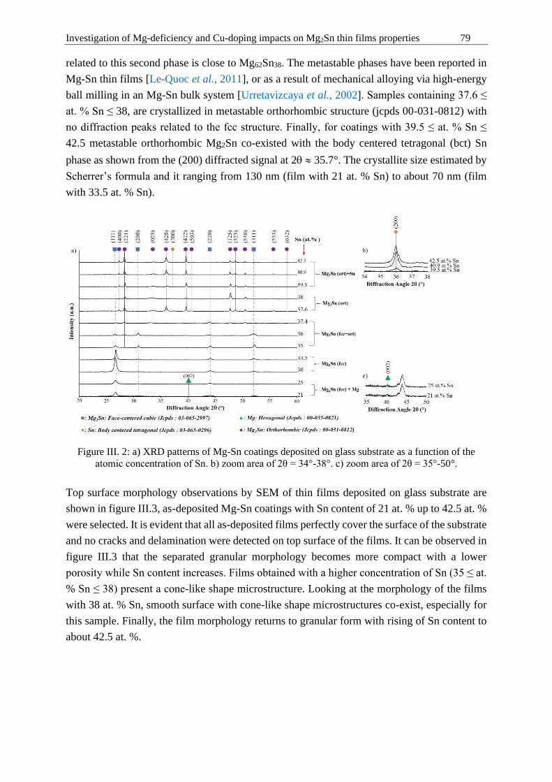
Investigation of Mg-deficiency and Cu-doping impacts on Mg2Sn thin films properties 79
related to this second phase is close to Mg62Sn38. The metastable phases have been reported in
Mg-Sn thin films [Le-Quoc et al., 2011], or as a result of mechanical alloying via high-energy
ball milling in an Mg-Sn bulk system [Urretavizcaya et al., 2002]. Samples containing 37.6 ≤
at. % Sn ≤ 38, are crystallized in metastable orthorhombic structure (jcpds 00-031-0812) with
no diffraction peaks related to the fcc structure. Finally, for coatings with 39.5 ≤ at. % Sn ≤
42.5 metastable orthorhombic Mg2Sn co-existed with the body centered tetragonal (bct) Sn
phase as shown from the (200) diffracted signal at 2 35.7°. The crystallite size estimated by
Scherrer’s formula and it ranging from 130 nm (film with 21 at. % Sn) to about 70 nm (film
with 33.5 at. % Sn).
Figure III. 2: a) XRD patterns of Mg-Sn coatings deposited on glass substrate as a function of the
atomic concentration of Sn. b) zoom area of 2θ = 34°-38°. c) zoom area of 2θ = 35°-50°.
Top surface morphology observations by SEM of thin films deposited on glass substrate are
shown in figure III.3, as-deposited Mg-Sn coatings with Sn content of 21 at. % up to 42.5 at. %
were selected. It is evident that all as-deposited films perfectly cover the surface of the substrate
and no cracks and delamination were detected on top surface of the films. It can be observed in
figure III.3 that the separated granular morphology becomes more compact with a lower
porosity while Sn content increases. Films obtained with a higher concentration of Sn (35 ≤ at.
% Sn ≤ 38) present a cone-like shape microstructure. Looking at the morphology of the films
with 38 at. % Sn, smooth surface with cone-like shape microstructures co-exist, especially for
this sample. Finally, the film morphology returns to granular form with rising of Sn content to
about 42.5 at. %.

Investigation of Mg-deficiency and Cu-doping impacts on Mg2Sn thin films properties 80
Figure III. 3: SEM micrographs of Mg-Sn as-deposited films on glass substrate: Top surface images
vs. composition.
Figure III.4 reveals brittle fracture cross section observations of the films as a function of Sn
atomic concentration. It can be seen that coatings containing 21 ≤ at. % Sn ≤ 25 present a
relatively more porous granular aspect compared to other samples. By increasing the atomic
concentration of Sn until 30-35 at. %, the morphology changes to slight columnar and becomes
denser. The coating with 36 at. % Sn exhibits a relatively dense columnar morphology with
submicron in-plan featured sizes. The coatings containing 38 ≤ at. % Sn ≤ 42.5 show a
completely dense and compact morphology. No cracks are detected and a good adhesion
between coating and substrate is observed. It is well known that, regarding to high energy of
sputtered atoms, adhesion of the films deposited by sputtering is much better than those
obtained with other deposition methods, e.g. by thermal evaporation [Le-Quoc et al., 2011].
The films thickness measured by SEM is relatively homogeneous with an average of about 1
µm. This value is in good agreement with those measured by profilometry. The deposition rate
is about 0.05 (µm. min-1).

Investigation of Mg-deficiency and Cu-doping impacts on Mg2Sn thin films properties 81
Figure III. 4: SEM cross section micrographs of Mg-Sn thin films deposited on glass substrate.
III.2.2. Measurement of electronic transport properties of Mg2Sn thin films
The electronic transport properties of Mg-Sn thin films vs. temperature, were measured by Hall
effect and in the air. Figure III.5 illustrates the dependency of DC electrical resistivity of the
films with Sn content of 33.5 at. % up to 42.5 at. % as a function of temperature. As shown for
the films with 33.5 at. % Sn, which are well-crystallized in fcc Mg2Sn structure, the electrical
resistivity decreases as the temperature rises. It is well known that the electrical resistivity of
semiconductor materials decreases with increasing temperature [Lardjane et al., 2015]. For the
films with 35 ≤ at. % Sn ≤ 37.6, where the crystal structure changes from cubic to orthorhombic
structure, the variation of electrical resistivity becomes quite constant as a function of the
temperature. For the coatings containing 39.5 ≤ at. % Sn ≤ 42.5 with the orthorhombic structure
and presence of Sn secondary phase, the electrical resistivity is enhanced by the temperature,
that is associated to the metallic behavior related to the excess of Sn atoms. It is important to
note that, especially for the sample with 36 at. % Sn, the electrical resistivity remains relatively
constant vs. temperature (between 30 °C and 200 °C) with a value of about 2.31×10⁻⁵ Ω m.

Investigation of Mg-deficiency and Cu-doping impacts on Mg2Sn thin films properties 82
Figure III. 5: DC electrical resistivity of Mg2Sn thin films vs. temperature
The variation of carrier concentration vs. temperature for the film with different Sn
concentrations is shown in figure III.6. It is important to highlight that the film carrier
concentration increases with Sn content in the films. Liu et al. [Liu et al., 2016] reported the
influence of intrinsic point defects on electronic transport properties of Mg2X (X = Si, Ge, Sn)
systems. They showed that Mg vacancies and interstitial Mg are assumed to be the main defects
in Mg2X compounds according to their relatively low formation energies. Mg vacancies and
interstitials Mg behave as acceptor and donor sites, respectively. We suppose that the increase
of carrier concentration in Mg2Sn films, while Sn content rises, can be explained by the
formation of Mg vacancies. The carrier concentration for all coatings is enhanced by increasing
the temperature and reaches the highest values (more than 1027 m-3) for the films containing
42.5 at. % Sn (the same order of magnitude of carrier concentrations in metals).
Figure III. 6: Carrier concentration of Mg2Sn thin films vs. temperature

Investigation of Mg-deficiency and Cu-doping impacts on Mg2Sn thin films properties 83
Figure III.7 shows the variation of carrier mobility of the films vs. temperature. The carrier
mobility of all films decreases while the temperature rises. The carrier mobility is relatively
low for the films adopting the Mg2Sn cubic structure (33.5 at. % Sn). As the formation of
metastable orthorhombic Mg2Sn begins, carrier mobility increases (35 ≤ at. % Sn ≤ 37.6) and
the highest carrier mobility is obtained for the single phase orthorhombic Mg2Sn with 37.6 at.
% Sn. Finally, a further increase of the Sn content (≥ 39.5 at. %) leads to a drastic decrease of
the film carrier mobility. It is assigned to the presence of secondary Sn phase in these samples
as detected by XRD patterns (figure III.2).
Figure III. 7: Carrier mobility of Mg2Sn thin films vs. temperature
Figure III.8 reveals the variation of carrier mobility as a function of the carrier concentration.
For all films, this ratio decreases by increasing the temperature. It is clear that the highest ratios
of carrier mobility to carrier concentration are obtained for the films exhibiting the
orthorhombic structure. With the presence of Sn secondary phase in the films (at. % Sn ≥ 39.5),
this ratio starts to decrease and the films tend to behave like a metallic compound.
Figure III. 8 : Carrier mobility vs. carrier concentration for Mg2Sn thin films

Investigation of Mg-deficiency and Cu-doping impacts on Mg2Sn thin films properties 84
III.2.3. Measurement of thermoelectric properties of Mg2Sn thin film
The thermoelectric properties were measured in vacuum (about 10-4 Pa) at different
temperatures using TFA device, on Linseis chips covered by Mg-Sn thin films.
Figure III.9 shows electrical conductivity of Mg2Sn thin films vs. temperature. The film
electrical conductivity decreases by increasing the atomic concentration of Sn from 21 to 33.5
at. % (Mg2Sn fcc structure). Then, the films conductivity enhances while the concentration of
Sn increases up to 42.5 at. % and the crystal structure changes to orthorhombic Mg2Sn structure.
Both samples with an excess of Mg or Sn show the highest values of electrical conductivity
(films with Sn = 21 at. % and Sn = 42.5 at. %, respectively). The highest electrical conductivity
is related to the coating containing 21 at. % Sn (6.2×10⁶ S m-1 at 30 °C).
Figure III. 9: Electrical conductivity of Mg2Sn thin films measured by TFA device under vacuum vs.
temperature
Figure III.10 shows the variations of Seebeck coefficient vs. temperature. For all coatings,
Seebeck coefficient is positive throughout the measured temperature range. All films are p-type
semiconductors [Du et al., 2015]. The Seebeck coefficient and carrier concentration are
inversely proportional. This can be explained based on the following equation:
𝑆 ∝ ±𝑘𝐵 (𝑟 − ln 𝑛) / 𝑒 (III.1)
Where kB is the Boltzmann’s constant (1.38×10⁻²³ J K-1), e the elementary charge (1.6×10⁻¹⁹ A
s), r is the scattering factor, and n the carrier concentration (m-3). The scattering factor r signifies
the exponent of the relaxation time vs. energy and is supposed to be constant. Therefore, as the
carrier concentration rises, the Seebeck coefficient decreases [Gao et al., 2011; An et al., 2012].
With respect to Le-Quoc et al. [Le-Quoc et al., 2012], the films with lower atomic concentration
of Sn, exhibits lower Seebeck coefficient and higher electrical conductivity. At room
temperature, the Seebeck coefficient varies from 2.1 µV K−1 to 174 µV K−1, which is at least
three times smaller than the value reported for the bulk Mg2Sn materials in the same
temperature range [Chen et al., 2009; Chen et al., 2010]. The films containing secondary phases
of Mg or Sn show relatively low Seebeck values compared to single phase Mg2Sn films. The

Investigation of Mg-deficiency and Cu-doping impacts on Mg2Sn thin films properties 85
coating with 35 ≤ at. % Sn ≤ 36 and containing a mixture of cubic and orthorhombic structures
exhibits the highest Seebeck coefficient (152 µV K−1) at high temperature. The sample with
cubic structure (at. % Sn ≈ 33.5) present the highest value of Seebeck coefficient (174 µV K−1)
at low temperature and while temperature rises, the coefficient decreases.
Figure III. 10: Seebeck coefficient of Mg2Sn thin films measured by TFA device in vacuum vs.
temperature
Figure III.11 represents the evolution of thermal conductivity of thin films vs. temperature. It
is clear that while eliminating the secondary phase of Mg and rising Sn concentration, the
thermal conductivity significantly reduces. The highest thermal conductivity is related to the
coating containing 21 at. % Sn (7.9 W m−1 K−1). The thermal conductivity for coating with 42.5
at. % Sn is more affected by the variation of temperature. As previously noted, lower thermal
conductivity value can be expected for deposited thin films with polycrystalline structure
compared to the same materials in bulk form. Chen and Savvides [Chen et al., 2010] reported
the thermal conductivity about 5-15 Wm-1K-1 for bulk Mg2Sn.
Figure III. 11: Thermal conductivity of Mg2Sn thin films measured by TFA device in vacuum vs.
temperature

Investigation of Mg-deficiency and Cu-doping impacts on Mg2Sn thin films properties 86
Figure III.12 indicates the variation of figure of merit (ZT) as a function of the temperature for
Mg-Sn thin films. The samples containing 21 at. % Sn up to 25 at. % Sn show low ZT values
as they behave like metal compounds due to the presence of Mg secondary phase. By increasing
the content of Sn from 30 at. % to 33.5 at. %, (samples with fcc structure and without secondary
phase of Sn), ZT values slightly enhance but remain relatively stable vs. temperature. By
changing the crystal structure from cubic to orthorhombic, (35 ≤ at. % Sn ≤ 38), the ZT values
notably enhance and as shown in figure III.12, ZT increases with temperature. The maximum
ZT value is obtained for thin films containing 36 at. % Sn with Mg2Sn cubic and orthorhombic
mixed crystal structures (ZT ~ 0.26 at 200 °C). The ZT slightly decreases for the film with 38
at. % Sn (with only the orthorhombic Mg2Sn structure) and drops in the case of the film with
42.5 at. % Sn (orthorhombic Mg2Sn structure + Sn secondary phase).
Figure III. 12: Figure of merit ZT of Mg2Sn thin films measured by TFA device in vacuum vs.
temperature
III.2.4. Thermal stability of the Mg2Sn thin films
As shown in section III.2.1, the Mg-Sn films structure is affected by the Sn atomic
concentration. It was shown that Mg2Sn structure was changed from stable face-centered cubic
to metastable orthorhombic structure while the content of Sn in the films increased. Three films
with different Sn atomic concentrations and crystal structure deposited on glass substrate were
selected and annealed in vacuum (10-4 Pa) at different temperatures (from 50 °C up to 600 °C
with an incremental step of 50 °C) with a dwell time of 2 hours. These films are:
• Mg-Sn (33.5 at. % Sn) with face centered cubic structure
• Mg-Sn (36 at. % Sn) with mixture of face centered cubic and orthorhombic structure
• Mg-Sn (38 at. % Sn) with orthorhombic structure
Such treatments were performed to determine the stability and structural decomposition
temperature limit for each sample.

Investigation of Mg-deficiency and Cu-doping impacts on Mg2Sn thin films properties 87
• Mg2Sn (Sn 33.5 at. %):
Figure III.13 shows the XRD patterns of the film with 33.5 at. % Sn after annealing treatments
up to 600 °C under vacuum. Until 500 °C, the face centered cubic structure (jcpds 03-065-2997)
remains. As the annealing temperature rises to 500 °C, the slight right shift of the diffraction
peaks appears in this film, which might be related to the stress relaxation during annealing
treatment. For temperatures higher than 500 °C, the cubic Mg2Sn structure vanishes and
decomposition of Mg2Sn phase occurs which is leading to Mg and Sn formation. The (200)
diffracted signal related to Sn phase (jcpds 03-065-0296) coexists with (100) and (110)
diffracted peaks of Mg related to (hcp) and (bcc) phases, respectively.
Figure III. 13: X-ray diffraction patterns of the film with 33.5 at. % Sn deposited on glass substrate
and post annealed in vacuum (10-4 Pa) for 2 h at different temperatures.
• Mg2Sn (36 at. % Sn):
Figure III.14 shows the XRD patterns of film with 36 at. % Sn, annealed in vacuum at different
temperatures up to 600 °C. Until 300 °C, the cubic Mg2Sn structure coexists with (211)
diffracted peak related to the metastable orthorhombic Mg2Sn phase. For temperatures in-
between 350-500 °C, the metastable orthorhombic phase disappears and the well-crystallized
stable cubic Mg2Sn structure is obtained. As this sample has a non-stoichiometric composition
(Sn-rich content) in the temperature above 350 °C, the excess of Sn begins to release with the
appearance of Sn secondary phase as shown by (200) diffracted signal related to Sn phase at 2θ
≈ 37°. For temperatures higher than 500 °C, the cubic Mg2Sn structure vanishes (decomposition
of Mg2Sn phase leading to Mg and Sn formation). The (200) diffracted signal related to Sn
phase (jcpds 03-065-0296) coexists with (100) and (110) diffracted peaks of Mg related to (hcp)
and (bcc) phases, respectively.

Investigation of Mg-deficiency and Cu-doping impacts on Mg2Sn thin films properties 88
Figure III. 14: X-ray diffraction patterns of the film with 36 at. % Sn deposited on glass substrate and
post annealed in vacuum (10-4 Pa) for 2 h at different temperatures.
Figure III.15 shows the top surface observation (a) and X-ray mapping (b) of the film with 36
at. % Sn deposited on a glass substrate after 2 h annealing at 600 °C under vacuum (10-4 Pa). It
is noticeable that the film morphology completely changed. Sn atoms segregated from Mg2Sn
layer and an entirely film decomposition happened. As confirmed by X-ray mapping image
heterogeneous Sn and Mg areas are formed. This result is in good agreement with XRD patterns
of this sample after an annealing at the temperature above 500 °C (figure III.14).
Figure III. 15 : (a) Top surface observation and (b) X-ray mapping of the film with 36 at. % Sn
deposited on glass substrate after 2 h annealing at 600°C under vacuum (10-4 Pa).
• Mg2Sn (38 at. % Sn):
Figure III.16 shows the XRD patterns of the film with 38 at. % Sn after annealing treatments
up to 600 °C under vacuum. Until 150 °C, the orthorhombic Mg2Sn structure remains. As this
sample has a non-stoichiometric composition (Sn-rich content) in the temperature above 200
°C, the excess of Sn begins to release with the appearance of Sn secondary phase ((200)
diffracted signal related to Sn phase is detected at 2θ ≈ 37°). For temperatures in-between 300-

Investigation of Mg-deficiency and Cu-doping impacts on Mg2Sn thin films properties 89
400 °C, the cubic Mg2Sn structure coexists with (211) and (200) diffracted peaks related to the
metastable orthorhombic Mg2Sn phase and Sn secondary phase, respectively.
For temperatures 450-500 °C, the cubic Mg2Sn structure coexists with the metastable
orthorhombic Mg2Sn phase and body centered tetragonal Sn phase. Furthermore, the diffracted
peaks (100) and (110) related to Mg (hcp) and (bcc) phases respectively, appear in this
temperature range.
For temperatures higher than 550 °C, the cubic and orthorhombic Mg2Sn structures vanish
(decomposition of Mg2Sn phase leading to Mg and Sn formation). The (200) diffracted signal
related to Sn phase (jcpds 03-065-0296) coexists with (100) and (110) diffracted peaks of Mg
related to (hcp) and (bcc) phases, respectively.
Figure III. 16: X-ray diffraction patterns of the film with 38 at. % Sn deposited on glass substrate and
post annealed under vacuum (10-4 Pa) for 2 h at different temperatures.
III.3. Cu-doping impact on stoichiometry and Mg-deficiency thin films
Cu-doped Mg-Sn coatings were synthesized by co-sputtering of Mg, Sn and Cu (purity 99.9 at.
%, = 50 mm, thickness= 3 mm) targets in a pure argon atmosphere. The Mg and Sn targets
were powered by pulsed (DC) power supplies (Pinnacle, Advanced Energy). The Cu target was
powered by DC power supply (MDX 500, Advanced Energy). The main sputtering parameters
are summarized in Table III.2
Table III. 2: Sputtering parameters used during deposition of Cu-doped Mg2Sn coatings.
Target
Discharge
Power Frequency Toff
Ar Flow
Rate
Working
Pressure
Run
Duration
Draw
Distance
(DT-S)
(W) (kHz) (µs) (sccm) (Pa) (min) (mm)
Sn 50 and 56 50
50
0
4
4
0
50 0.41 20 60 Mg
Cu
73
0→1

Investigation of Mg-deficiency and Cu-doping impacts on Mg2Sn thin films properties 90
Figure III.17 repeats the evolution of the atomic concentration of Sn measured by EDS analyses
for each coating deposited on fused quartz as a function of the power ratio applied to each target
(PSn/PMg) presented in the previous part of this study (figure III.1). In this part, the sputtering
parameters of closed symbols are selected and the power discharge on Cu target was adjusted
to investigate the effect of the Cu doping (0, 0.5 and 1.5 at. % Cu) on stoichiometry and Mg
deficiency thin films.
Figure III. 17: Evolution of the Sn atomic concentration in the films measured by Energy-Dispersive
X-ray Spectroscopy (EDS) vs. sputtering power ratio applied to Mg and Sn targets (figure III.1 was
repeated). The red dotted line is a guide for the eye. Sputtering parameters of closed symbols are used in
this part to investigate the effect of the Cu doping on stoichiometry and Mg deficiency thin films.
Table III.3 shows the thickness and composition of both groups of samples. The chemical
composition of coatings deposited on fused quartz were measured by EDS analyses. Three
different zones of each coating were selected for EDS measurements and the average
concentration was calculated. EDS analyses show relatively homogeneous composition on the
entire surface of deposited thin films.
Table III. 3 : Composition and thickness of deposited Cu-doped Mg2Sn thin films
Group no. Sample
no.
Mg content
(at. %)
Sn content
(at. %)
⌈𝑴𝒈⌉
[𝑺𝒏]
Cu content
(at. %)
Thickness
(±20 nm)
Group I
Sample # 1 67±1 33±1 2 0.0 1000
Sample # 2 67±1 33±1 2 0.5 970
Sample # 3 66±1 33±1 2 1.5 1200
Group II
Sample # 4 64±1 36±1 1.75 0.0 1000
Sample # 5 63±1 36±1 1.75 0.5 1100
Sample # 6 63±1 35±1 1.75 1.5 1100
III.3.1. Structural and morphological characterization of Cu-doped Mg2Sn thin films
Figure III.18 displays the X-ray diffraction patterns of both groups as a function of Cu atomic
concentrations. The XRD results show a well-crystallized stable cubic (fcc) Mg2Sn structure
for undoped films of group I. For Cu doped films of group I, the diffracted peaks of cubic
Mg2Sn phase (jcpds 03-065-2997) coexists with (422) and (221) very weak diffracted signals

Investigation of Mg-deficiency and Cu-doping impacts on Mg2Sn thin films properties 91
related to the metastable orthorhombic Mg2Sn phase (jcpds 00-031-0812). For all samples of
group II, the diffracted peaks of cubic Mg2Sn (jcpds 03-065-2997) coexist with (400), (221)
and (422) diffracted signals corresponding to the metastable orthorhombic phase (jcpds 00-031-
0812). Assuming a stoichiometry close to Mg62Sn38, the proportion of orthorhombic phase
determined from the chemical content of the film is less than 5% in the undoped samples of
group I and reaches 57 % in the undoped sample of group II. In addition, it is worth of noting
that the cubic phase in group I crystallizes mostly along the (111) preferential direction while
this preferential direction becomes less important in group II. For all doped films of both
groups, even with a large amount of Cu (as high as 1.5 at. %), no traces of secondary phase
related to Cu is observed.
Figure III. 18: XRD patterns of Mg-Sn coatings deposited on glass substrate as a function of the
atomic concentration of Cu. a) group I with ⌈Mg⌉
[Sn]= 2, b) group II with
⌈Mg⌉
[Sn]= 1.75
Figure III.19 reveals top surface morphology and brittle fracture cross-section observations of
thin films deposited on glass substrates by SEM. For group I, the granular morphology with a
lateral grain size of about 70 nm is evident for the undoped samples and by raising the content
of Cu, separated granular morphology becomes more compact with a lower porosity and cone-
like shape microstructures. The brittle fracture cross section observation of undoped film in
group I, shows a relatively dense morphology with some porosities and open spaces. The
structure becomes more columnar with a less porous microstructures for the films with 0.5 and
1.5 at. % of Cu of group I.
The small cone-like morphology can be seen for undoped films of group II. By Cu-doping, the
smooth surface with a larger cone-like shape is observed for the other films of group II. The
undoped thin film of group II, exhibits a relatively dense and columnar morphology. The films
with 0.5 and 1.5 at. % Cu of group II show a more compact and larger columnar morphology.
It is worth noting that all samples perfectly cover the surface of the substrate and no cracks and
delamination were detected on the top surface of the films, and a good adhesion between films
and substrate was observed.

Investigation of Mg-deficiency and Cu-doping impacts on Mg2Sn thin films properties 92
Figure III. 19: SEM micrographs of deposited films on glass substrate and SEM cross section
micrographs vs. atomic concentration of Cu. a) group I with ⌈Mg⌉
[Sn]= 2, b) group II with
⌈Mg⌉
[Sn]= 1.75.
III.3.2. Measurement of electronic transport properties of Cu-doped Mg2Sn thin films
The electronic transport properties of Cu-doped Mg2Sn thin films vs. temperature were
measured in air by Hall effect. The temperature dependence of electrical conductivity is shown
in figure III.20. For all films, the electrical conductivity increases with the temperature. No
changes corresponding to some chemical or structural modifications occur in the films. In group
I, by raising the Cu content in the films, the electrical conductivity increases. For the film with
1.5 at. % Cu of group I, the electrical conductivity reaches 1.89×10⁴ S m-1 at 200 °C while for
undoped sample of this group, it does not exceed 1.53×10⁴ S m-1 at 200 °C. It is worth to note
that for all samples of group I, the electrical conductivity increases with temperature which
indicates a semiconducting-like behaviors. In group II, undoped and doped films with 1.5 at. %
Cu show the highest electrical conductivity (4.5×10⁴ S m-1 at 200 °C). The film with 0.5 at. %
Cu has a relatively low electrical conductivity (2.26×10⁴ S m-1 at 200 °C) in group II. For the
undoped film of group II, the electrical conductivity remains constant vs. temperature.

Investigation of Mg-deficiency and Cu-doping impacts on Mg2Sn thin films properties 93
Figure III. 20 : Electrical conductivity of Cu doped (0, 0.5 and 1.5 at. % Cu) thin films of group I and
group II vs. temperature.
Figure III.21 shows the variation of carrier concentration vs. temperature for all samples. For
the undoped films of group I, the carrier concentration is relatively constant while for Cu-doped
samples, the carrier concentration increases with temperature. The carrier concentration is close
to 4×1026 m-3 at 200 °C for the film of group I with 1.5 at. % Cu. Surprisingly, the undoped
sample of group II exhibits the highest carrier concentration when increasing temperature and
the lowest carrier concentration is obtained for the sample with 0.5 at. % Cu in this group. The
carrier concentration gradually increases with temperature for all films of group II. As
previously discussed in III.2.2., Liu et al. [Liu et al., 2016] reported the effect of intrinsic point
defects on electronic transport properties of Mg2X (X = Si, Ge, Sn) systems. They showed that
Mg vacancies and interstitial Mg are supposed to be the main defects in Mg2X compounds due
to their relatively low formation energies. Mg vacancies and interstitials behave as acceptor and
donor sites, respectively. As a consequence, the higher value of carrier concentration for
undoped Mg2Sn films of group II compared with the undoped films of group I can be explained
by the formation of Mg vacancies which is more probable in the films containing an excess of
Sn. Furthermore, Tani and Kido [Tani et al., 2012] studied the formation energy of impurities
in Mg2Sn. They reported the Cu-substitution preference on Mg-site or Sn-site is highly
dependent on Sn content in Mg2Sn system. In the case of Sn-rich Mg2Sn materials (such
compounds are similar to that of group II), Cu substitution occurs mainly in Mg-sites and
reduces the carrier concentration. Choi et al. [Choi et al., 2012] assumed that in Sn-rich systems,
Cu atoms are trapped at the grain boundary and do not react with the Mg2Sn matrix which
probably happens for the films of group II as the grain boundary increases due to the coexistence
of two phases in this group. They also supposed that Cu atoms do not substitute to Sn atoms,
but react with Sn atoms, forming CuxSny trace phase. Furthermore, the formation of this new
second phase disturbs the formation of the p-type Mg-deficient in Mg2Sn phase. As shown in
figure III.18.b, by increasing the Cu-doping in films of group II, the intensity of the cubic phase
increases compared to the undoped films of this group. It can be assumed that by forming

Investigation of Mg-deficiency and Cu-doping impacts on Mg2Sn thin films properties 94
CuxSny trace phase (not detectable by XRD analysis), the Mg/Sn ratio changes, and these
samples are not Sn-rich enough compared to the undoped films of this group. These may also
explain why there is no enhancement of the carrier concentration in the films of group II by Cu
doping. In group I, it is supposed that Cu reacts with Mg and leads to Mg-deficient state. The
orthorhombic phase is formed (figure III.18.a) and consequently improves the carrier
concentration in films of group I. Despite these considerations, the evolution of the carrier
concentration with the Cu content in group II is still an open question.
Figure III. 21: Carrier concentration of Cu doped Mg-Sn (0, 0.5 and 1.5 at. % Cu) thin films in groups
I and II vs. temperature.
The temperature dependence of carrier mobility for all samples is shown in figure III.22. The
higher carrier mobility is observed for the films of group II explaining the higher electrical
conductivity of the group II. It was already observed in section III.2.2. that the metastable
orthorhombic phase exhibits a higher carrier mobility than the cubic Mg2Sn phase. The carrier
mobility for the undoped film of group I containing the fcc structure is nearly unaffected by the
temperature while it slightly decreases for doped-films of this group, probably due to the charge
carriers scattering on the Cu ions with their increasing content, and/or because of their “open”
morphology. As a result, carrier mobility in Cu-doped or Mg-deficient thin films is more
sensitive to the film composition and defects than temperature.
The electronic transport mechanisms are then ruled by chemical and structural defects than
electron-phonon scattering as typically described in many semiconducting materials containing
a low concentration of defects. That’s explain why the conductivity slope is smaller for the
coating containing 1.5 at. % Cu than for the undoped coating. In undoped Mg2Sn systems, the
carrier mobility is relatively low for the films with the cubic structure (group I), carrier mobility
increases in undoped films of group II because of the formation of metastable orthorhombic
Mg2Sn. It is important to remember that the highest carrier mobility is observed for the single
phase orthorhombic Mg2Sn (figure III.7). In group II, the lowest carrier mobility is obtained for

Investigation of Mg-deficiency and Cu-doping impacts on Mg2Sn thin films properties 95
undoped films, and in contrary with the behavior of the films in group I, it can be observed that
the Cu doping in the films of group II leads to an enhancement of the carrier mobility.
Figure III. 22: Carrier mobility of Cu doped Mg-Sn (0, 0.5 and 1.5 at. % Cu) thin films in group I and
II vs. temperature.
III.3.3. Measurement of optic bandgap of Cu-doped Mg2Sn thin films
From Hall effects measurements, resistivity and Hall coefficient are connected via the following
relation:
𝜌 =1
𝑅𝐻𝑒 (III.2)
Where RH is the Hall coefficient (Ω m T-1), e the elementary charge (1.6×10⁻¹⁹ As) and ρ the
hole carrier concentration (m-3) which is extracted from the measured Hall coefficient. The Hall
mobility µH (m2 V-1 s-1) is given by the following equation:
µ𝐻 = 𝑅𝐻 . 𝜎 (III.3)
Where σ is the electrical conductivity (S m-1). Assuming that in the intrinsic temperature range,
the hole concentration ρ of a semiconductor is almost equal to the electron concentration:
𝜌 = 𝑛 = 2(𝐾𝐵 𝑇
2𝜋ћ2)3
2⁄ (𝑚𝑒 𝑚ℎ)3
4⁄ exp(−𝐸𝑔
2𝐾𝐵 𝑇) (III.4)
Where KB is the Boltzmann constant (1.38×10⁻²³ J K-1), ћ the reduced Planck’s constant
(1.05×10⁻³⁴ J s), me the effective mass of electron (kg), mhthe effective mass of hole and Eg the
bandgap (eV). The hole and electron mobilities both vary as Tr. Then by combining equations
(III.3-III.4), plotting ln[σT-(r+1.5)] vs. T-1 is linear with -Eg
2KB as the slope [Chen et al., 2010]. By
using the experimental data, the undoped sample in group I, r takes -2.8 and by plotting the

Investigation of Mg-deficiency and Cu-doping impacts on Mg2Sn thin films properties 96
ln[σT1.3] vs. 1000/T, the bandgap energy is about 0.30 eV, which is in good agreement with the
literature (figure III.23) [Savvides et al., 2010].
Figure III. 23 : plot of ln(σT1.3) as a function of reciprocal temperature for un-doped Mg2Sn in group I
([Mg]
[Sn]= 2)
For other samples, the calculated bandgap energy is not relevant. Figure III.24 shows the
Kubelka-Munk transformed absorption spectra for both groups.
Figure III. 24 : Kubelka-Munk transformed absorption spectra used to estimate the bandgap of Cu-
doped Mg-Sn (0, 0.5 and 1.5 at. % Cu) thin films a) in group I and b) in group II.
The optical bandgap estimation for all samples by using the Kubelka-Munk method are
summarized in table III.4.
Table III. 4 : Bandgap of thin films obtained by the Kubelka-Munk’s method (± 0.02 eV)
Samples Group I Bandgap (eV) Samples Group II Bandgap (eV)
0 at. % Cu 0.46 0 at. % Cu 0.47
0.5 at. % Cu 0.47 0.5 at. % Cu 0.48
1.5 at. % Cu 0.48 1.5 at. % Cu 0.47
The optical bandgap energy of undoped stoichiometric Mg2Sn is about 0.46 eV, which is a little
higher than previously reported values (0.33-0.36 eV) [Tani et al., 2012]. When the charge

Investigation of Mg-deficiency and Cu-doping impacts on Mg2Sn thin films properties 97
carrier concentration increases with the Cu content in stoichiometric films of group I, the
apparent optical bandgap energy slightly increases as well. In the case of group II, the optical
bandgap remains quite constant with Cu doping. Again, the optical bandgap behavior vs. Cu
doping is unclear, probably due to the alteration of the optical properties with the crystallization
of the orthorhombic phase induced by the Mg content lowering.
III.3.4. Measurement of thermoelectric properties of Cu-doped Mg2Sn thin films
The thermoelectric properties were measured in vacuum (about 10-4 Pa) at different
temperatures by means of TFA device on Linseis chip covered by undoped or Cu-doped Mg-
Sn thin films.
For group I, the electrical conductivity increases by raising the Cu concentration (figure III.25).
For group II, the conductivity is relatively the same for undoped films and sample doped with
0.5 at. % Cu but surprisingly in the case of the film doped with 1.5 at. % Cu, the electrical
conductivity decreases. It is right to note that all samples of group II display the highest
electrical conductivity over the entire temperature range compared to the samples of group I.
Electrical conductivity of the films measured in vacuum displays lower values compare to
measurements performed in air.
Figure III. 25: Electrical conductivity of Cu doped Mg-Sn (0, 0.5 and 1.5 at. % Cu) thin films in group
I and II vs. temperature.
The same dependencies of the film’s electrical conductivity vs. temperature are observed in
vacuum and air for the films of group I. The films are thermally activated, and Cu doping in
stoichiometric compounds leads to higher electrical conductivity. However, in the groups II,
the electrical conductivity variations vs. temperature in air and vacuum do not exhibit the
similar behaviors while Cu concentration increases. Therefore, samples with 0.5 and 1.5 at. %
Cu of group II, deposited on glass substrate were annealed in vacuum (10-4 Pa) and in air at 200
°C for 2 hours. Such treatments were performed to better understand the difference between

Investigation of Mg-deficiency and Cu-doping impacts on Mg2Sn thin films properties 98
electrical conductivity values measured in air and in vacuum in this group. Figure III.26
illustrates top surface morphology observations by SEM of annealed films. The film containing
0.5 at. % Cu remains compact after annealing (air and vacuum) while the sample with 1.5 at.
% Cu only remains compact in air. With 1.5 at. % Cu and after annealing under vacuum, the
films become more columnar with separated open spaces. As expected, the film with a compact
morphology should lead to a better electrical and thermal conductivity [Le-Quoc et al., 2012].
Figure III. 26: SEM micrographs of deposited films with 0.5 and 1.5 at. % Cu of group II on glass
substrate: As deposited and after 2h annealing in air and in vacuum.
The crystallographic structure of samples with 0.5 and 1.5 at. % Cu of group II, after annealing
at 200 °C for 2 hours under in air and vacuum was checked by XRD analysis as shown in figure
III.27. The crystallite size was estimated using Scherrer's formula. In the case of the sample
with 1.5 at. % Cu annealed under vacuum, the crystallite size decreases when annealing
temperature rises. Consequently, the difference between electrical conductivity values
measured in air and in vacuum can be related to this unusual variation of crystallite size.
Figure III. 27 : a) X-ray diffraction patterns of the deposited films with 0.5 and 1.5 at. % Cu of group
II on glass substrate: As deposited and after 2h annealing in air and in vacuum, b) grain size of the
films with 0.5 and 1.5 at. % Cu of group II after 2h annealing in air and under vacuum.

Investigation of Mg-deficiency and Cu-doping impacts on Mg2Sn thin films properties 99
Figure III.28 presents the variation of the Seebeck coefficient vs. temperature. All samples can
be considered as p-type conductors since the Seebeck coefficient is positive throughout the
temperature range. The highest value of Seebeck coefficient belongs to undoped films with S
close to 174 µV K-1 at 30 °C. The Seebeck coefficient decreases with temperature for undoped
Mg2Sn films of group I. For the sample containing 0.5 at. % Cu (group I), the Seebeck
coefficient first slightly increases up to 100 °C and then decreases. The Seebeck coefficient for
sample with 0.5 at. % Cu of group I reaches the same value as the undoped film at 120 °C and
remains higher than it for the upper temperature. For the film with 1.5 at. % Cu of group I, the
Seebeck coefficient increases with temperature and never exceeds 97 µV K-1. This sample
shows the lowest Seebeck coefficient, despite Cu doping. In group II, the undoped sample and
the film with 0.5 at. % Cu show relatively the same Seebeck coefficient through the temperature
range. The sample with 1.5 at. % Cu presents the highest Seebeck coefficient of group II with
S = 130 µV K-1 at 30 °C. It is also interesting to note some correlations between the evolution
of the carrier concentration (Figure III.21) and Seebeck coefficient (Figure III.27) as a function
of the temperature and Cu concentration. It is commonly reported that the Seebeck coefficient
of semiconductors typically decreases when the concentration of charge carriers increases
[Levin, 2016]. Assuming a simple model of electron transport, Seebeck coefficient S is
inversely proportional to the hole concentration p (S 1/p2/3) for a given temperature [Snyder
et al., 2008]. Our results well agree with these theoretical models where Cu-doped Mg2Sn films
exhibit a clear decrease of Seebeck coefficient as the hole concentration rises and by changing
the temperature, particularly for the films of group I.
Figure III. 28: Seebeck coefficient of Cu doped Mg-Sn (0, 0.5 and 1.5 at. % Cu) thin films in group I
and II vs. temperature.
Figure III.29 illustrates the thermal conductivity for all samples as a function of the temperature.
For group I, the thermal conductivity increases with Cu doping. The sample with 1.5 at. % Cu
shows the highest thermal conductivity of about 1.85 W m-1 K-1. For undoped sample, the

Investigation of Mg-deficiency and Cu-doping impacts on Mg2Sn thin films properties 100
thermal conductivity raises with temperature. The film with 0.5 at. % Cu exhibits a relatively
constant thermal conductivity until 140 °C. In group II, the thermal conductivity of undoped
sample drops with temperature till 150 °C and goes up again. For the sample with 0.5 at. % Cu
of group II, the thermal conductivity rises as the temperature reaches 140 °C and then reduces.
The sample containing 1.5 at. % Cu offers the lowest thermal conductivity. For this sample, the
thermal conductivity decreases till 60 °C and then for temperature above goes up.
Figure III. 29: Thermal conductivity of Cu doped Mg-Sn (0, 0.5 and 1.5 at. % Cu) thin films in group I
and II vs. temperature.
Figure III.30 shows the variation of figure of merit ZT vs. temperature for all thin films. For the
samples of group I, ZT is the highest with 0.07 at 200 °C. This ZT value is related to the sample
with 0.5 at. % Cu, which is about four times more than the ZT for undoped sample of this group.
This enhanced ZT value is related to a high and stable Seebeck coefficient combined with
moderate electrical conductivity. The ZT value of the film containing 1.5 at. % Cu of group I is
almost the same as the undoped film of the same group, because of the limited Seebeck
coefficient. The samples of group II show higher ZT values. The highest ZT of group II is
obtained for undoped and doped with 0.5 at. % Cu which is about 0.27 at 200 °C. The sample
with 1.5 at. % Cu shows higher ZT values at a lower temperature compared with other samples
of the same group. It is believed that these ZT improvements of group II are due to the
metastable phase exhibiting higher electrical mobility rather than the change in the preferential
orientation of the cubic phase.

Investigation of Mg-deficiency and Cu-doping impacts on Mg2Sn thin films properties 101
Figure III. 30: Figure of merit ZT of Cu doped Mg-Sn (0, 0.5 and 1.5 at. % Cu) thin films in group I
and II vs. temperature.
III.4. Conclusion
In the first part of this chapter, Mg-Sn thin films (21 ≤ at. % Sn ≤ 42.5) were successfully
deposited by magnetron co-sputtering in an argon atmosphere. The film structure is strongly
affected by the Sn atomic concentration. Thin films containing 21≤ at. % Sn ≤ 25 have fcc
Mg2Sn structure with a secondary phase of Mg. The latter vanishes and fcc Mg2Sn structure
remains stable in the range of 30 ˂ at. % Sn < 33.5. Thin films with 35 ≤ at. % Sn ≤ 37.4 exhibit
a mixture of cubic and orthorhombic Mg2Sn phases. Films with 37.6 up to 38 at. % Sn adopt
the orthorhombic Mg2Sn structure and finally for the coatings containing 39.5≤ at. % Sn ≤ 42.5,
orthorhombic Mg2Sn structure with secondary phase of Sn co-exist. Thermal stability of the
Mg-Sn films with different crystal structure was studied under vacuum. Such treatments were
performed to determine the stability and structural decomposition temperature limit for each
sample. In this group the film with 33.5 at. % Sn (fcc) showed the highest thermal stability. For,
this sample till 500 °C, the face centered cubic structure remains. For temperatures higher than
500 °C, the cubic Mg2Sn structure vanishes and decomposition of Mg2Sn phase occurs which
is leading to Mg and Sn formation. For the film with 36 at. % Sn (fcc + orthorhombic) until
300°C, the mixed structure remains stable. The orthorhombic phase transforms to cubic while
annealing temperature increases from 350 °C to 500 °C and the secondary phase of Sn began
to form. Finally, at temperatures higher than 500 °C, Mg2Sn thin film completely decomposes
into Mg and Sn. For the sample with 38 at. % Sn (orthorhombic), till 150 °C, the orthorhombic
Mg2Sn structure remains. As this sample has a non-stoichiometric composition (Sn-rich
content) in the temperature above 200 °C, the excess of Sn begins to release as Sn secondary
phase. For temperatures in-between 300-400 °C, the cubic Mg2Sn structure coexists with the
metastable orthorhombic Mg2Sn phase and Sn secondary phase, respectively. For temperatures
450-500 °C, the cubic Mg2Sn structure coexists with the metastable orthorhombic Mg2Sn phase
Investigation of Mg-deficiency and Cu-doping impacts on Mg2Sn thin films properties 102
and body centered tetragonal Sn phase. For temperatures higher than 550 °C, the cubic and
orthorhombic Mg2Sn structures vanish and decomposition of Mg2Sn phase was leading to Mg
and Sn formation.
Thermoelectric properties of the films with different structures were discussed as a function of
the temperature. With formation of orthorhombic Mg2Sn structure, ZT value is enhanced
compared to that of the film with cubic Mg2Sn structure. ZT values increase with temperature
for orthorhombic Mg2Sn coatings. The highest values of ZT = 0.26 is obtained at 200 °C while
cubic and orthorhombic Mg2Sn phases (36 at. % Sn) coexist in the films.
In the second part of this chapter, two groups of Mg-Sn thin films were deposited by co-
sputtering of Mg, Sn and Cu targets in an argon atmosphere. The effect of Mg-deficiency and
Cu-doping on thermoelectric properties of Mg-Sn was studied. Group I with ⌈Mg⌉/[Sn] =2 and
group II with ⌈Mg⌉/[Sn] =1.75 were doped by different Cu concentrations (0, 0.5 and 1.5 at.
%). Only the film with 0 at. % Cu of group I showed a stable face-centered cubic structure. For
other samples in both groups, a mixture of face-centered cubic and metastable orthorhombic
phases coexists. The thermoelectric properties of both groups were discussed in a wide range
of temperatures (30-200 °C) to investigate the influence of Cu-doping. It is shown that the Cu
introduction in stoichiometric and cubic Mg2Sn compound improves the electronic properties,
as expected, but also the thermal conductivity and in contrast to the decrease of the Seebeck
coefficients leading to the improvement of the thermoelectric properties in a restraint range.
The highest ZT value of about 0.07 was obtained at 200 °C with 0.5 at. % of Cu in group I. The
films of group II with a Mg-deficiency shows a different behavior. They exhibit higher
electrical conductivities due to a better carrier mobility. Thermal conductivities and Seebeck
coefficients of the same order of magnitude than in stoichiometric films were obtained in group
II. These features develop higher thermoelectric properties, almost 4 times higher (ZT = 0.27 at
200 °C for the film doped with 0.5 at. % of Cu). It is believed that the mixture of cubic and
orthorhombic phases contributes to the achievement of a higher carrier mobility.
Thermoelectric properties of the Mg2Sn films improved while a mixture of cubic and
orthorhombic coexist.

Investigation of Mg-deficiency and Cu-doping impacts on Mg2Sn thin films properties 103
III.5. References
An, T. H., Choi, S. M., Kim, I. H., Kim, S. U., Seo, W. S., Kim, J. Y., & C. Park, (2012).
Thermoelectric properties of a doped Mg2Sn system. Renewable Energy, 42, 23-27.
Chen, H. Y., & Savvides, N. (2009). Microstructure and thermoelectric properties of n- and p-
type doped Mg2Sn compounds prepared by the modified Bridgman method. Journal of
Electronic Materials, 38, 1056-1060.
Chen, H. Y., & Savvides, N. (2010). High quality Mg2Sn crystals prepared by RF induction
melting. Journal of Crystal Growth, 312, 2328-2334.
Chen, H. Y., Savvides, N., Dasgupta, T., Stiewe, C., & Mueller, E. (2010). Electronic and
thermal transport properties of Mg2Sn crystals containing finely dispersed eutectic structures.
Physica Status Solidi a, 207, 2523–2531.
Choi, S. M., An, T. H., Seo, W. S., Park, C., Kim, I. H., & Kim, S. U. (2012). Doping effects
on thermoelectric properties in the Mg2Sn system. Journal of Electronic Materials, 41, 1071-
1076.
Du, Z. L. H., Gao, L., & Cui, J. L. (2015). Thermoelectric performance of quaternary
Mg2(1+x)Si0.2Ge0.1Sn0.7 (0.06 ≤ x ≤ 0.12) solid solutions with band convergence. Current Applied
Physics, 15, 784-788.
Gao, H. L., Liu, X. X., Zhu, T. J., Yang, S. H., & Zhao, X. B. (2011). Effect of Sb doping on
the thermoelectric properties of Mg2Si0.7Sn0.3 solid solutions. Journal of Electronic Materials
40, 830-834.
Lardjane, S., Arab Pour Yazdi, M., Martin, N., Bellourd, C., Fenineche, N. E., Schuler, A.,
Merad, G., & Billard, A. (2015). Structural, electrical and magnetic characterization of in-situ
crystallized ZnO:Co thin films synthesized by reactive magnetron sputtering. Materials
Chemistry and Physics,161, 26-34.
Le-Quoc, H., Lacoste, A., Béchu, S., Bès, A., Bourgault, D., & Fruchart, D. (2012). Deposition
of thin films of Mg2Si1-xSnx solid solution by plasma-assisted co-sputtering. Journal of Alloys
and Compounds, 538, 73–78.
Le-Quoc, H., Lacoste, A., Hlil, E. K., Bès, A., Vinh, T. T., Fruchart, D., & Skryabina, N.
(2011). Thin films of thermoelectric compound Mg2Sn deposited by co-sputtering assisted by
multi-dipolar microwave plasma. Journal of Alloys and Compounds, 509, 9906-9911.
Levin, E. M. (2016). Charge carrier effective mass and concentration derived from combination
of Seebeck coefficient and 125Te NMR measurements in complex tellurides. Physical Review B
- Condensed Matter and Materials Physics, 93, 245202.
Liu, X., Xi, L., Qiu, W., Yang, J., Zhu, T., Zhao, X., & Zhang, W. (2016). Significant roles of
intrinsic point defects in Mg2X (X = Si, Ge, Sn) thermoelectric materials. Advanced Electronic
Materials, 2, 1500284-1500294.
Savvides, N., & Chen, H. Y. (2010). Thermal conductivity and other transport properties of
Mg2Sn: Ag crystals. Journal of Electronic Materials, 39, 2136–2141.

Investigation of Mg-deficiency and Cu-doping impacts on Mg2Sn thin films properties 104
Snyder, G. J., & Toberer, E. S. (2008). Complex thermoelectric materials. Nature materials, 7,
105-114.
Tani, J. I., & Kido, H. (2012). Impurity doping into Mg2Sn: A first-principles study. Physical
Review B - Condensed Matter and Materials Physics, 407, 3493–3498.
Urretavizcaya, G., & Meyer, G. O. (2002). Metastable hexagonal Mg2Sn obtained by
mechanical alloying. Journal of Alloys and Compounds, 339, 211–215.

Chapter 4
Thermoelectric performance of Mg2Si1-xSnx
and Mg2Ge1-xSnx solid solutions
Table of contents
IV.1. Introduction ................................................................................................................................ 108
IV.2. Mg2Si1-xSnx thin films ................................................................................................................ 108
IV.2.1 Structural and morphological characterization of Mg2Si1-xSnx thin films ................................ 110
IV.2.2. Measurement of electronic transport properties of Mg2Si1-xSnx thin films ......................... 111
IV.2.3. Measurement of thermoelectric properties of Mg2Si1-xSnx thin film .................................. 113
IV.2.4. Thermal stability of the Mg2Si1-xSnx thin films .................................................................. 116
IV.3. Ge-doped Mg2Si0.35Sn0.65 thin films ........................................................................................... 117
IV.3.1. Structural and morphological characterization of Ge-doped Mg2Si0.35Sn0.65 thin films ...... 117
IV.3.2. Measurement of electronic transport properties of Ge-doped Mg2Si0.35Sn0.65 thin films .... 119
IV.3.3. Measurement of thermoelectric properties of Ge-doped Mg2Si0.35Sn0.65 thin films ............ 121
IV.3.4. Thermal stability of the Ge-doped Mg2Si0.35Sn0.65 thin films .............................................. 123
IV.4. Mg2Ge1-xSnx thin films ............................................................................................................... 124
IV.4.1 Structural characterization and thermal stability of the Mg2Ge1-xSnx thin films .................. 125
IV.4.2 Morphological characterization of Mg2Ge1-xSnx thin films ................................................. 127
IV.4.3. Measurement of electronic transport properties of Mg2Ge1-xSnx thin films........................ 128
IV.4.4. Measurement of thermoelectric properties of Mg2Ge1-xSnx thin films ............................... 130
IV.5. Conclusion ................................................................................................................................. 133
IV.6. References .................................................................................................................................. 135
List of Figures
Figure IV. 1: Evolution of stoichiometric ratio of Mg, Si, and Sn in Mg2Si1-xSnx thin films vs. sputtering power ratio applied on each target ............................................................................. 109
Figure IV. 2: a) X-ray diffraction patterns for thin films of Mg2Si1-xSnx, b) Evolution of Mg2Si1-xSnx
lattice parameters (a) vs. Sn concentration, and c) Evolution of Mg2Si1-xSnx crystallite size
estimated by Scherrer's formula vs. Sn concentration ................................................................ 110
Figure IV. 3: SEM micrographs of films deposited on glass substrate (a-c) and SEM cross section
micrographs (d-f) of Mg2Si1-xSnx with different compositions. .................................................. 111
Figure IV. 4: DC electrical resistivity vs. temperature of Mg2Si1-xSnx thin films measured in air. .... 112
Figure IV. 5: Carrier concentration vs. temperature of Mg2Si1-xSnx thin films in air. ......................... 112

Figure IV. 6: Carrier mobility vs. temperature of Mg2Si1-xSnx thin films in air. ................................. 113
Figure IV. 7: Electrical conductivity vs. temperature of Mg2Si1-xSnx thin films measured in vacuum by
TFA device. ................................................................................................................................ 113
Figure IV. 8: X-ray diffraction patterns for thin films after 2 h annealing in air and in vacuum: a)
Mg2Si0.7Sn0.3, b) Mg2Si0.35Sn0.65 and c) Mg2Si0.3Sn0.7 ................................................................. 114
Figure IV. 9: Seebeck coefficient vs. temperature of Mg2Si1-xSnx thin films measured by TFA device
in vacuum. .................................................................................................................................. 114
Figure IV. 10: Thermal conductivity vs. temperature of Mg2Si1-xSnx thin films measured by TFA
device in vacuum. ....................................................................................................................... 115
Figure IV. 11: Figure of merit (ZT) of Mg2Si1-xSnx thin films measured by TFA device in vacuum vs.
temperature (a) Zoom area of ZT variation vs. Temperature (b) ................................................ 115
Figure IV. 12: X-ray diffraction patterns of the Mg2Si1-xSnx thin films deposited on glass substrate and
post annealed in vacuum (10-4 Pa) for 2 h at different temperatures: a) Mg2Si0.7Sn0.3, b)
Mg2Si0.35Sn0.65, and c) Mg2Si0.3Sn0.7 ........................................................................................... 116
Figure IV. 13: XRD patterns of Ge-doped Mg2Si0.35Sn0.65 coatings deposited on glass substrate as a
function of the Ge atomic concentration. ................................................................................... 118
Figure IV. 14: SEM micrographs of Mg2Si0.35Sn0.65 thin films doped with different Ge concentrations
deposited on glass substrate (a-d) and SEM cross section micrographs (e-h) vs. Ge atomic
concentration. ............................................................................................................................. 119
Figure IV. 15: DC electrical conductivity of Ge-doped Mg2Si0.35Sn0.65 thin films vs. temperature
measured in air by hall effect ...................................................................................................... 120
Figure IV. 16: Carrier concentration vs. temperature of Ge-doped Mg2Si0.35Sn0.65 thin films in air. .. 120
Figure IV. 17: Carrier mobility vs. temperature of Ge-doped Mg2Si0.35Sn0.65 thin films in air. .......... 121
Figure IV. 18: Electrical conductivity vs. temperature of Ge-doped Mg2Si0.35Sn0.65 thin films measured
by TFA device in vacuum........................................................................................................... 121
Figure IV. 19: Seebeck coefficient vs. temperature of Ge-doped Mg2Si0.35Sn0.65 thin films measured by
TFA device in vacuum. .............................................................................................................. 122
Figure IV. 20: Thermal conductivity of Ge-doped Mg2Si0.35Sn0.65 thin films measured by TFA device
in vacuum vs. temperature .......................................................................................................... 123
Figure IV. 21 : Figure of merit (ZT) vs. temperature of Ge-doped Mg2Si0.35Sn0.65 thin films measured
by TFA device in vacuum (a) and zoom of ZT variation vs. temperature (b) ............................ 123
Figure IV. 22: X-ray diffraction patterns of the Ge-doped Mg2Si0.35Sn0.65 thin films deposited on glass
substrate and post annealed in vacuum (10-4 Pa) for 2 h at different temperatures. Doped with: a)
1 at. % Ge, b) 4 at. % Ge, and c) 7 at. % Ge .............................................................................. 124
Figure IV. 23: X-ray diffraction patterns of as deposited Mg2Ge1-xSnx on glass substrate and post
annealed in vacuum (10-4 Pa) for 2 h at different temperatures. a) Mg2Ge, b) Mg2Ge0.5Sn0.5, c)
Mg2Ge0.3Sn0.7, and d) Mg2Sn. ..................................................................................................... 126
Figure IV. 24 : X-ray diffraction patterns for thin films of Mg2Ge1-xSnx. ........................................... 127
Figure IV. 25: SEM micrographs of films deposited on glass substrate (a-d) and SEM cross section
micrographs (e-h) of Mg2Ge1-xSnx with different compositions. ................................................ 128
Figure IV. 26: DC electrical conductivity of Mg2Ge1-xSnx thin films vs. temperature ....................... 129
Figure IV. 27: Carrier concentration of Mg2Ge1-xSnx thin films vs. temperature ................................ 129
Figure IV. 28: Carrier mobility vs. temperature of Mg2Ge1-xSnx thin films. ....................................... 130
Figure IV. 29: Electrical resistivity vs. temperature of Mg2Ge1-xSnx thin films measured by TFA
device under vacuum. ................................................................................................................. 131
Figure IV. 30 : Seebeck coefficient vs. temperature of Mg2Ge1-xSnx thin films measured by TFA
device in vacuum. ....................................................................................................................... 131
Figure IV. 31 : Thermal conductivity vs. temperature of Mg2Ge1-xSnx thin films measured by TFA
device in vacuum. ....................................................................................................................... 132
Figure IV. 32: Figure of merit (ZT) vs. temperature of Mg2Ge1-xSnx thin films measured by TFA
device in vacuum. ....................................................................................................................... 132

List of Tables
Table IV. 1 : Sputtering parameters used during deposition of Mg2Si1-xSnx coatings. ....................... 108
Table IV. 2 : Composition and thickness of deposited Mg2Si1-xSnx thin films ................................... 109
Table IV. 3 : Bandgap of Mg2Si1-xSnx thin films obtained by Kubelka-Munk’s method ( 0.02 eV) 109
Table IV. 4 : Sputtering parameters used during deposition of Ge-doped Mg2Si0.35Sn0.65 coatings. ... 117
Table IV. 5 : Composition and thickness of Ge-doped Mg2Si0.35Sn0.65 ............................................... 117
Table IV. 6 : Sputtering parameters used during deposition of Mg2Ge1-xSnx coatings. ...................... 125
Table IV. 7 : Composition and thickness of Mg2Ge1-xSnx thin films .................................................. 125

Thermoelectric performance of Mg2Si1-xSnx and Mg2Sn1-xGex solid solutions 108
IV.1. Introduction
Different strategies for improving ZT was discussed in chapter I.9. As previously noted, one of
the strategies to improve ZT was the structural modification of promising compounds by
introducing point defects through the isostructural solid solutions formation. The solid solution
features make changes in the crystal lattice (i.e., disorder) which produces strong phonon
scattering centers and reduce thermal conductivity [Kanatzidis, 2010].
In the first part of this chapter, Mg2Si1-xSnx solid solutions thin films were synthesized by
magnetron co-sputtering of Mg, Sn and Si targets in an argon atmosphere. The aim of this
investigation is to understand the influence of chemical composition on the films electronic
transport and thermoelectric properties. Thermal stability of the films was studied after
annealing in vacuum (10-4 Pa) at different temperatures.
In the second part Mg2Si0.35Sn0.65 has been selected and doped by different atomic
concentrations of Ge (0, 1, 4, and 7 at. %), in order to improve ZT in the system. The structure
and morphology of the films were investigated as a function of the Ge atomic concentration.
The film charge carrier concentration and mobility were measured to explain the electronic
transport behavior and the effect of Ge-doping on thermoelectric properties of Mg2Si0.35Sn0.65
were discussed in a range of temperatures: 30-200 °C. Thermal stability of Ge doped films were
explored after annealing in vacuum (10-4 Pa) at different temperatures.
In the last part, Mg2Ge1-xSnx (x = 0, 0.5, 0.7) thin films were deposited by magnetron co-
sputtering of Mg, Sn and Ge targets in an argon atmosphere. The thermal stability of the film
was examined after annealing in vacuum (10-4 Pa) at different temperatures. The influence of
chemical composition and crystal structure on the films electronic transport and thermoelectric
properties was discussed.
IV.2. Mg2Si1-xSnx thin films
For obtaining thin films Mg2Si1-xSnx (x= 0.3, 0.65, 0.7) with different chemical compositions,
the power was fixed at 50 W for Mg target, 20 W for Sn target and was systematically changed
on Si target from 44 to 85 W to tune the coating composition. Argon flow rate was 50 sccm and
working pressure was kept at 0.41 Pa during deposition. Substrates (Special chip produced by
Linseis, as well as alumina pellet and glass microscope slides) were placed on the substrate
holder at 60 mm from the substrate holder axis and all depositions were carried out at floating
temperature (Tsubstrate < 70 °C). The main sputtering parameters are summarized in Table IV.1.
Table IV. 1: Sputtering parameters used during deposition of Mg2Si1-xSnx coatings.
Ar flow rate (sccm) 50 Target Mg Sn Si
Working pressure (Pa) 0.41 Discharge power (W) 50 20 44→85
Draw distance (DT-S) (mm) 60 Frequency (kHz) 50 50 50
Run duration (min) 25 𝑻𝒐𝒇𝒇 (µs) 4 4 4

Thermoelectric performance of Mg2Si1-xSnx and Mg2Sn1-xGex solid solutions 109
Table IV.2 shows the chemical composition and thickness of all coatings measured by EDS
analyses and profilometer, respectively. Three different zones of each coating deposited on
alumina pellet were selected for EDS measurements and the average concentration was
calculated. It can be noted that EDS analyses show relatively homogeneous composition on the
entire surface of deposited thin films. According to the film thickness the average rate of
deposition is about 2.5 µm h-1.
Table IV. 2: Composition and thickness of deposited Mg2Si1-xSnx thin films
Sample no. Mg content
(at. %)
Si content
(at. %)
Sn content
(at. %)
Nominal
composition
Thickness
(±20 nm)
Sample # 1 67 ±1 22 ± 0.5 11± 0.5 Mg2Si0.7Sn0.3 0.82
Sample # 2 67 ± 1 12 ± 0.5 21 ± 0.5 Mg2Si0.35Sn0.65 0.87
Sample # 3 67 ± 1 11 ± 0.5 22 ± 0.5 Mg2Si0.3Sn0.7 0.87
Figure IV.1 illustrates the stoichiometric ratio of Mg, Si, and Sn of all films deposited on
alumina pellet measured by EDS measurements as a function of applied power to each target
𝑃𝑆𝑖/(𝑃𝑀𝑔 + 𝑃𝑆𝑛) during sputtering process. For all films [Mg]/([Si]+[Sn]) is kept almost about
2. These results show that as the applied power ratio 𝑃𝑆𝑖/(𝑃𝑀𝑔 + 𝑃𝑆𝑛) increases, films become
Si-rich following a linear evolution.
Figure IV. 1: Evolution of stoichiometric ratio of Mg, Si, and Sn in Mg2Si1-xSnx thin films vs. sputtering power ratio applied on each target
The optical bandgap estimation for Mg2Si1-xSnx thin films by using the Kubelka-Munk method
are summarized in table IV.3.
Table IV. 3 : Bandgap of Mg2Si1-xSnx thin films obtained by Kubelka-Munk’s method ( 0.02 eV)
Sample Bandgap (eV) by Kubelka-
Munk
Bandgap (eV)
[Santos et al., 2018]
Mg2Si0.7Sn0.3 0.54 0.5 Mg2Si0.35Sn0.65 0.46 0.46 Mg2Si0.3Sn0.7 0.48 0.5

Thermoelectric performance of Mg2Si1-xSnx and Mg2Sn1-xGex solid solutions 110
For the antifluorite structure of Mg2Sn and Mg2Si the band gap energy is reported about 0.35
eV and 0.77 eV, respectively. The bandgap energy, highly depends on the composition in solid
solution Mg2Si1-xSnx and has a nonlinear character. Theoretically, the lower bandgap energy
can be expected for the Sn-rich films [Zaitsev et al, 2006; Liu et al., 2012; Santos et al., 2018].
As it is shown in table IV.3, the best bandgap convergence occurs in Mg2Si0.35Sn0.65 films with
the same value reported by Santos et al. [Santos et al., 2018].
IV.2.1 Structural and morphological characterization of Mg2Si1-xSnx thin films
Figure IV.2 a presents the X-ray diffraction patterns of as-deposited coatings. All diffraction
peaks are related to the face centered cubic (fcc) antifluorite structure with the space group
𝐹𝑚3𝑚 (jcpds: 01-089-4254). The most intense peak (2𝜃 ≈ 27°) is positioned between those
of Mg2Sn (jcpds: 03-065-2997) (2𝜃 ≈ 26°) and Mg2Si (jcpds: 03-065-9365) (2𝜃 ≈ 28°),
confirming the formation of the solid solutions. The peaks gradually shift towards lower angle
by increasing Sn content, as Sn has larger ionic radius than Si. The lattice parameter (a) is
calculated using Bragg’s equation and approximately follow Vegard’s law. The lattice
parameter increases almost linearly with raising the Sn content in the films (figure IV.2 b)
[Kamila et al., 2019]. Figure IV.2 c presents the evolution of crystallite size estimated by
Scherrer's formula for as-deposited films vs. Sn concentration (at. %). Mg2Si0.35Sn0.65 has the
largest crystallite size (~57 nm). Mg2Si0.3Sn0.7 and Mg2Si0.7Sn0.3 have relatively the same
crystallite size about 40 nm.
Figure IV. 2: a) X-ray diffraction patterns for thin films of Mg2Si1-xSnx, b) Evolution of Mg2Si1-xSnx
lattice parameters (a) vs. Sn concentration, and c) Evolution of Mg2Si1-xSnx crystallite size estimated
by Scherrer's formula vs. Sn concentration
Figure IV.3 reveals top surface morphology and brittle fracture cross section observations by
SEM of thin films deposited on glass substrates. The smooth surface with granular features was
observed for the film Mg2Si0.7Sn0.3. The granular morphology with some porosities and open
spaces can be seen for Mg2Si0.35Sn0.65. By increasing the Sn content, the morphology becomes

Thermoelectric performance of Mg2Si1-xSnx and Mg2Sn1-xGex solid solutions 111
more compact for Mg2Si0.3Sn0.7. Brittle fracture cross section observations show a relatively
dense columnar morphology for films Mg2Si0.7Sn0.3 and Mg2Si0.35Sn0.65. The film Mg2Si0.3Sn0.7
presents a dense featureless microstructure with no growing defects. All samples perfectly
cover the surface of the substrate and no cracks and delamination are detected on the top surface
of the films. A good adhesion between films and substrate is also observed.
Figure IV. 3: SEM micrographs of films deposited on glass substrate (a-c) and SEM cross section
micrographs (d-f) of Mg2Si1-xSnx with different compositions.
IV.2.2. Measurement of electronic transport properties of Mg2Si1-xSnx thin films
The electronic transport properties of Mg2Si1-xSnx thin films vs. temperature were measured in
air by Hall effect. Figure IV.4 presents the dependency of DC electrical conductivity of the
Mg2Si1-xSnx films as a function of the temperature. For all films, the electrical conductivity
increases with the temperature, which indicates a semiconducting-like behavior [Khan et al.,
2013]. Mg2Si0.7Sn0.3 shows the lowest electrical conductivity value. It does not exceed 1.4×10³
S m-1 at 200 °C because in Mg2Si1-xSnx solid solution electrical conductivity decreases by Si
content [Le-Quoc et al., 2012]. Surprisingly, Mg2Si0.35Sn0.65, displays higher electrical
conductivity throughout the measured temperature range compared with Mg2Si0.3Sn0.7 while the
Sn content is lower. This unusual behavior could be explained by the larger crystallite size of

Thermoelectric performance of Mg2Si1-xSnx and Mg2Sn1-xGex solid solutions 112
Mg2Si0.35Sn0.65 thin film (figure IV.2 c). The electrical conductivity value for this film is about
1.26×10³ S m-1 at 30 °C and reaches to 4.31×10³ S m-1 at 200 °C.
Figure IV. 4: DC electrical resistivity vs. temperature of Mg2Si1-xSnx thin films measured in air.
The variation of carrier concentration vs. temperature for the Mg2Si1-xSnx films is shown in
figure IV.5. The carrier concentration is improved by temperature for all films. For
Mg2Si0.3Sn0.7 and Mg2Si0.35Sn0.65, almost the same carrier concentration, about 7.5×1025 m-3 is
obtained at 40 °C. For the film Mg2Si0.35Sn0.65, the carrier concentration increases with sharper
slope, and reaches 5.6×1026m-3 at 170 °C. The Mg2Si0.7Sn0.3 film shows the lowest carrier
concentration throughout the measured temperature, and do not exceed 7.63×1025 m-3 at 200
°C.
Figure IV. 5: Carrier concentration vs. temperature of Mg2Si1-xSnx thin films in air.
Figure IV.6 presents the variation of carrier mobility vs. temperature for the Mg2Si1-xSnx films.
Mg2Si0.35Sn0.65 has the lowest carrier mobility (4.4×10⁻⁵ m2 V-1 s-1 at 30 °C). The highest carrier
mobility obtained for Mg2Si0.7Sn0.3 is about 9.9 × 10⁻⁵ m2 V-1 s-1 at 200 °C. As it can be seen in
figure IV.6, the variation of carrier mobility by temperature is insignificant for all samples. So,
we can conclude that electrical conductivity is ruled by the carrier concentration rather than
carrier mobility in these samples.

Thermoelectric performance of Mg2Si1-xSnx and Mg2Sn1-xGex solid solutions 113
Figure IV. 6: Carrier mobility vs. temperature of Mg2Si1-xSnx thin films in air.
IV.2.3. Measurement of thermoelectric properties of Mg2Si1-xSnx thin film
The thermoelectric properties were measured in vacuum (about 10-4 Pa) at different
temperatures using TFA device, on Linseis chips covered by Mg2Si1-xSnx thin films. The
temperature dependence of electrical conductivity for Mg2Si1-xSnx under vacuum are plotted in
figure IV.7. The electrical conductivity measured under vacuum raises with temperature for all
samples with the same trend of the electrical conductivity measured in air (figure IV.4).
Mg2Si0.35Sn0.65 shows the highest electrical conductivity (𝜎 ≈1.5×10³ S m-1 at 200 °C) and
Mg2Si0.7Sn0.3 exhibits the lowest electrical conductivity for the whole investigated temperature
range.
Figure IV. 7: Electrical conductivity vs. temperature of Mg2Si1-xSnx thin films measured in vacuum by
TFA device.
Mg2Si0.35Sn0.65 and Mg2Si0.3Sn0.7 exhibit a lower electrical conductivity in vacuum compared to
the same measurements performed in air. The crystallographic structure of all samples after
annealing at 200 °C for 2 hours in air and in vacuum was checked by XRD (figure IV.8). For
all samples, the films structures are relatively similar after annealing in air and in vacuum and
no secondary phases are observed. The average crystallite size was estimated using Scherrer's
formula. For Mg2Si0.35Sn0.65, the size is about 69 and 83 nm after annealing in vacuum and in
air, respectively. It is well known that, the electrical conductivity decreases by reducing the
crystallite size because of the carrier scattering enhancement at the grain boundaries [Satyala,
et al., 2012]. For Mg2Si0.3Sn0.7 and Mg2Si0.7Sn0.3 the average crystallite size was not changed

Thermoelectric performance of Mg2Si1-xSnx and Mg2Sn1-xGex solid solutions 114
significantly. Consequently, the difference between electrical conductivity values measured in
air and in vacuum for these samples should not be related to the variation of the average
crystallite size.
Figure IV. 8: X-ray diffraction patterns for thin films after 2 h annealing in air and in vacuum: a)
Mg2Si0.7Sn0.3, b) Mg2Si0.35Sn0.65 and c) Mg2Si0.3Sn0.7
The temperature dependence of Seebeck coefficient for Mg2Si1-xSnx are presented in figure
IV.9. The Seebeck coefficient is positive for Mg2Si0.3Sn0.7 and Mg2Si0.35Sn0.65 films showing
the p-type conduction. For these samples, the Seebeck coefficient value increases with
temperature up to 100 °C and then decreases. The Seebeck coefficient is negative throughout
the investigated temperature range for the film Mg2Si0.7Sn0.3, indicating an n-type conduction
for this film. For this sample, the absolute Seebeck coefficient value increases with temperature.
It is well known that the absolute Seebeck coefficient is proportional to the average energy of
electrons above the Fermi level. So the increase of the absolute Seebeck coefficient with
temperature occurs for the n-type sample of Mg2Si0.7Sn0.3. It can be related to this decrease of
Fermi level as the temperature raising [Gao et al., 2011]. The highest absolute Seebeck
coefficient of about 244 µV K-1 at 180 °C is obtained for n-type Mg2Si0.7Sn0.3.
Figure IV. 9: Seebeck coefficient vs. temperature of Mg2Si1-xSnx thin films measured by TFA device in
vacuum.
Figure IV.10 indicates the variation of thermal conductivity measured under vacuum by TFA
device vs. temperature for Mg2Si1-xSnx. The lowest thermal conductivity is observed for Mg2Si1-
xSnx compare to Mg2Sn thin films (paragraph III.2.3, figure III.11) due to effect of alloying on
their lattice thermal conductivity. The mass-difference scattering is considered as the main

Thermoelectric performance of Mg2Si1-xSnx and Mg2Sn1-xGex solid solutions 115
mechanism for decreasing the lattice thermal conductivity. Therefore, the large mass difference
between Si (28.1 a.m.u) and Sn (118.71 a.m.u) guaranties the reduction of thermal conductivity
[Bashir et al., 2014]. The lowest thermal conductivity of the solid solution (~ 1.8 W m-1 K-1) is
reported with a composition of 0.6 ≤ x ≤0.7, which is related to strong alloy scattering. The low
thermal conductivity can be expected for the thin films compared to the bulk material with the
same composition as the layer interfaces and the low grain size in thin films can act as scatter
centers for phonons [Vineis et al., 2010]. As shown by this figure, the thermal conductivity is
increased with temperature for Mg2Si0.3Sn0.7 and Mg2Si0.35Sn0.65 films. For Mg2Si0.7Sn0.3,
thermal conductivity is enhanced till 130 °C and then decreases drastically. This sample
exhibits the lowest thermal conductivity about 0.37 W m-1 K-1 at 30 °C, and it reaches 0.57 W
m-1 K-1 at 200 °C.
Figure IV. 10: Thermal conductivity vs. temperature of Mg2Si1-xSnx thin films measured by TFA
device in vacuum.
Figure IV.11 presents the temperature dependency of the figure of merit ZT of Mg2Si1-xSnx thin
films. The evolution of the ZT vs. temperature exhibits an exponential form for n-type
Mg2Si0.7Sn0.3 and reaches 3.6×10⁻² at 200 °C. The p-type Mg2Si0.3Sn0.7 has the lowest ZT all
over the temperature range. The ZT increases with temperature for this sample till 150 °C and
reaches 0.8×10⁻³ and then decreases. For another p-type Mg2Si0.35Sn0.65 film, the ZT enhances
with temperature till 160 °C and then remains quite constant (4×10⁻³ at 200 °C) for the rest of
the measured temperature range.
Figure IV. 11: Figure of merit (ZT) of Mg2Si1-xSnx thin films measured by TFA device in vacuum vs.
temperature (a) Zoom area of ZT variation vs. Temperature (b)

Thermoelectric performance of Mg2Si1-xSnx and Mg2Sn1-xGex solid solutions 116
IV.2.4. Thermal stability of the Mg2Si1-xSnx thin films
Mg2Si1-xSnx thin films deposited on glass substrate were annealed in vacuum (10-4 Pa) at
different temperatures (from 50 °C to 600 °C with an incremental step of 50 °C) with a dwell
time of 2 hours. Such treatments were performed to determine the stability and structural
decomposition temperature limit for each sample. Figure IV.12 illustrates the X-ray patterns of
the Mg2Si1-xSnx thin films after annealing treatments in vacuum up to 600 °C. Until 500 °C, the
face centered cubic structure (jcpds 01-089-4254) remains stable for all samples no matter of
their compositions. For the temperature in-between 300-450 °C, the (020) diffracted signal
related to Si phase (jcpds 01-089-9054) at 2θ ≈ 43° is only observed for Mg2Si0.7Sn0.3. At 550
°C, the cubic Mg2Si0.4Sn0.6 structure vanishes and decomposition of Mg2Si1-xSnx phase occurs
which corresponds to Mg, Si and Sn formation. The (200) diffracted signal related to Sn phase
(jcpds 03-065-0296) coexists with (110) diffracted peak of Mg related to (bcc) phase (jcpds 03-
065-0296) and (002) diffracted signal Si related to based-centered orthorhombic phase (jcpds
01-089-9054). For Mg2Si0.7Sn0.3 and Mg2Si0.3Sn0.7, the (200) diffracted peak of Si related to
hexagonal (jcpds 01-075-0841) is also observed.
Figure IV. 12: X-ray diffraction patterns of the Mg2Si1-xSnx thin films deposited on glass substrate and
post annealed in vacuum (10-4 Pa) for 2 h at different temperatures: a) Mg2Si0.7Sn0.3, b) Mg2Si0.35Sn0.65,
and c) Mg2Si0.3Sn0.7
As previously discussed, in paragraph I.9.4. (table I.8), many works have been focused on n-
type Mg2Si1-xSnx, while for developing a good thermoelectric generator, both n- and p-type
materials are required. It is important that both materials can be fabricated from similar

Thermoelectric performance of Mg2Si1-xSnx and Mg2Sn1-xGex solid solutions 117
compounds to reduce any thermal stress mismatch which can lead to failure of thermoelectric
module [An et al., 2012]. Therefore, for the next step, as Mg2Si0.35Sn0.65 shows p-type character
with higher ZT compare with other p-type film, this composition is selected and doped with Ge,
in order to improve its thermoelectric properties.
IV.3. Ge-doped Mg2Si0.35Sn0.65 thin films
For obtaining Ge-doped Mg2Si0.35Sn0.65 with different Ge concentrations, the power was fixed
at 50 W, 20 W, 50 W for Mg, Sn and Si targets, respectively. It was systematically changed on
Ge target from 2 to 4 W to tune the coating composition. The Mg, Si and Sn targets were
powered by pulsed direct current (DC) power supplies (Pinnacle, Advanced Energy), while the
Ge target was powered by DC power supply (MDX 500, Advanced Energy). The main
sputtering parameters are summarized in Table IV.4.
Table IV. 4 : Sputtering parameters used during deposition of Ge-doped Mg2Si0.35Sn0.65 coatings.
Ar flow rate (sccm) 50 Target Mg Sn Si Ge
Working pressure (Pa) 0.41 Discharge power (W) 50 20 50 2→4
Draw distance (DT-S) (mm) 60 Frequency (kHz) 50 50 50 0
Run duration (min) 25 𝑻𝒐𝒇𝒇 (µs) 4 4 4 0
Table IV.5 shows the chemical composition and thickness of each coatings measured by EDS
analyses and profilometer, respectively. Results obtained by EDS analyses confirms that a
relatively homogeneous composition is produced on the entire surface of deposited thin films.
Table IV. 5: Composition and thickness of Ge-doped Mg2Si0.35Sn0.65
Sample no. Mg Content
(at. %)
Si Content
(at .%)
Sn Content
(at. %)
Ge Content (at
.%)
Thickness
(µm) (±20nm)
Sample # 1 67±1 12±0.5 21±0.5 0 0.873
Sample # 2 67±1 10±0.5 22±0.5 1 ± 0.1 0.876
Sample # 3 65±1 10±0.5 21±0.5 4 ± 0.1 0.821
Sample # 4 64±1 11±0.5 18±0.5 7 ± 0.15 0.817
The optical bandgap energy for Ge-doped Mg2Si0.35Sn0.65 was determined by the Kubelka-
Munk’s method. The bandgap of undoped Mg2Si0.35Sn0.65 and the film with 1 at. % Ge is about
0.46 eV, which is in good agreement with literature [Santos et al., 2018]. By increasing Ge
content, the apparent optical bandgap energy increases as well. For the sample with 4 and 7 at.
% Ge, the bandgap values are about 0.56 and 0.52 eV, respectively.
IV.3.1. Structural and morphological characterization of Ge-doped Mg2Si0.35Sn0.65 thin
films
Figure IV.13 shows X-ray diffraction patterns of deposited films as a function of the Ge atomic
concentration. All diffraction peaks correspond to the face-centered cubic (fcc) antifluorite
structure with the space group 𝐹𝑚3𝑚 (jcpds: 01-089-4254). The most intense peak (2𝜃 ≈ 27°)
is located between those of Mg2Sn (jcpds: 03-065-2997) (2𝜃 ≈ 26°) and Mg2Si (jcpds: 03-065-
9365) (2𝜃 ≈ 28°), confirming the formation of the solid solutions. For all doped films and

Thermoelectric performance of Mg2Si1-xSnx and Mg2Sn1-xGex solid solutions 118
despite a large amount of Ge (as high as 7 at. %), no traces of a secondary phase related to Ge
is observed.
Figure IV. 13: XRD patterns of Ge-doped Mg2Si0.35Sn0.65 coatings deposited on glass substrate as a
function of the Ge atomic concentration.
Figure IV.14 reveals top surface morphology and brittle fracture cross section observations of
thin films deposited on glass substrates by SEM. The granular morphology with some porosities
and open spaces can be seen for undoped sample and film with 1 at. % of Ge. By increasing the
Ge content , the morphology becomes more compact.
Brittle fracture cross section observations show a relatively dense columnar morphology for
undoped and doped film with 1 at. % Ge. The film with 4 at. % of Ge has a denser microstructure
without distinct columns. For the film with 7 at. % Ge, the structure exhibits a dense and slightly
columnar structure. All samples perfectly cover the surface of the substrate and no cracks and
delamination were detected on the top surface of the films. A good adhesion between films and
substrate is also observed. The films’ thickness measured by SEM is relatively homogeneous,
and in good agreement with those measured by profilometry.

Thermoelectric performance of Mg2Si1-xSnx and Mg2Sn1-xGex solid solutions 119
Figure IV. 14: SEM micrographs of Mg2Si0.35Sn0.65 thin films doped with different Ge concentrations
deposited on glass substrate (a-d) and SEM cross section micrographs (e-h) vs. Ge atomic
concentration.
IV.3.2. Measurement of electronic transport properties of Ge-doped Mg2Si0.35Sn0.65 thin
films
The electronic transport properties of Ge-doped Mg2Si0.35Sn0.65 thin films vs. temperature were
measured in air by Hall effect. Figure IV.15 shows the variation of electrical conductivity as a
function of the temperature for Ge-doped Mg2Si0.35Sn0.65. For all films, the electrical
conductivity rises with the temperature, indicating a semiconducting-like behavior. With
addition of only 1 at. % of Ge, the film electrical conductivity decreases by about one order of
magnitude. This film shows the lowest electrical conductivity all over the measured temperature
range and finally reaches 1.31×10³ S m-1 at 200 °C. The undoped Mg2Si0.35Sn0.65 and the film
with 7 at. % Ge show almost the same electrical conductivity throughout the measured
temperature. The film with 4 at. % Ge exhibits the highest electrical conductivity at low
temperature and all over the measured temperature range. The highest electrical conductivity
for this sample is about 5.6×10³ S m-1 at 200 °C.

Thermoelectric performance of Mg2Si1-xSnx and Mg2Sn1-xGex solid solutions 120
Figure IV. 15: DC electrical conductivity of Ge-doped Mg2Si0.35Sn0.65 thin films vs. temperature
measured in air by hall effect
Figure IV.16 illustrates the temperature dependence of the carrier concentration of the thin
films. The carrier concentration rises with temperature for all samples. The undoped film
exhibits the highest carrier concentration value through the measured temperature range. The
lowest carrier concentration is obtained for the film with 1 at. % Ge at lower temperature and
does not exceed 3.0×1025 m-3. The carrier concentration increases with a sharp slope for the
sample with 7 at. % Ge and reaches to the same value as reported for the film with 4 at. % Ge
(7.7×1025 m-3 at 200 °C).
Figure IV. 16: Carrier concentration vs. temperature of Ge-doped Mg2Si0.35Sn0.65 thin films in air.
The variation of carrier mobility vs. temperature is shown in figure IV.17. The carrier mobility
rises by increasing Ge content. The film with 7 at. % Ge exhibits the highest carrier mobility at
the lower temperature while it drastically reduces with rising temperature. For the undoped
films and sample with 4 at. % Ge, the Hall mobility follows the form µ~𝑇0, determining neutral
impurity scattering mechanism, while for the film with 1 at. % Ge, the Hall mobility fits with
the µ~𝑇−1
2⁄ , signifying an optical phonon scattering mechanism. For the film with 7 at. % Ge,
the Hall mobility approximately follows µ~𝑇−3
2⁄ indicating that acoustical phonon is the
dominate scattering mechanism for this sample, respectively [Bashir et al., 2014; Chen et al.,
2015; Mao et al., 2018]. The highest carrier mobility is about 1.2×10⁻³ m2 V-1 S-1 at 30 °C for
the film with 7 at. % Ge.

Thermoelectric performance of Mg2Si1-xSnx and Mg2Sn1-xGex solid solutions 121
Figure IV. 17: Carrier mobility vs. temperature of Ge-doped Mg2Si0.35Sn0.65 thin films in air.
IV.3.3. Measurement of thermoelectric properties of Ge-doped Mg2Si0.35Sn0.65 thin films
The thermoelectric properties of Ge-doped Mg2Si0.35Sn0.65 were measured in vacuum (10-4 Pa)
at different temperatures by means of TFA device.
Figure IV.18 presents the temperature dependence of electrical conductivity for Ge-doped
Mg2Si0.35Sn0.65. The positive evolution of electrical conductivity for each film with temperature
happens due to an increase of the carrier concentration by intrinsic conduction which overcome
a decrease of the carrier mobility by electron-phonon scattering (figures IV.16 and 17). This
confirms that the films electrical conductivity vs. temperature is more affected by charge carrier
concentration than carrier mobility. The sample with 4 at. % Ge displays the highest electrical
conductivity in vacuum (6.5×10³ S m-1 at 200 °C).
Figure IV. 18: Electrical conductivity vs. temperature of Ge-doped Mg2Si0.35Sn0.65 thin films measured
by TFA device in vacuum.
Figure IV.19 reveals the variation of Seebeck coefficient vs. temperature for each sample. It’s
right to assume all films as a p-type semiconductor since the Seebeck coefficient is positive
throughout the temperature range. The undoped film exposes the lowest Seebeck coefficient
and addition of Ge leads to an improvement of the Seebeck coefficient.
The Seebeck coefficient and carrier concentration are inversely proportional. This can be
explained based on the following equation:

Thermoelectric performance of Mg2Si1-xSnx and Mg2Sn1-xGex solid solutions 122
𝑆 ∝ ±𝑘𝐵 (𝑟 − ln 𝑛)/𝑒 (IV.1)
Where 𝑘𝐵 is Boltzmann’s constant (1.38×10⁻²³ J K-1), e the elementary charge (1.6×10⁻¹⁹ As),
r is the scattering factor, and n the carrier concentration (m-3). The scattering factor r signifies
the exponent of the relaxation time vs. energy and is supposed to be constant. Therefore, as the
carrier concentration rises with temperature for each film, the Seebeck coefficient decreases
[Gao et al., 2011]. The film Seebeck coefficient increases about four times only with addition
of 1 at. % Ge and the highest Seebeck coefficient is about 248 µV K-1 at 30 °C for the film with
7 at. % Ge. For the films doped with 7 and 4 at. % Ge, the Seebeck coefficient decreases slightly
while for the film with 1 at. % Ge, it drops drastically with the temperature rising.
Figure IV. 19: Seebeck coefficient vs. temperature of Ge-doped Mg2Si0.35Sn0.65 thin films measured by
TFA device in vacuum.
Figure IV.20 illustrates the thermal conductivity for Ge-doped Mg2Si0.35Sn0.65 as a function of
the temperature. The thermal conductivity raises with temperature for the undoped film and
sample with 4 at. % Ge with neutral impurity scattering mechanism. The highest thermal
conductivity value (0.76 W m-1 K-1 at 200 °C) is obtained for the film with 4 at. % Ge. For the
samples with 1 and 7 at. % Ge, the thermal conductivity increases till 140 °C and then drops.
In the case of film with 1 at. % Ge, the low thermal conductivity is expected as this sample
shows the lowest electrical conductivity. For the films with 4 and 7 at. % Ge, both show a high
electrical conductivity. The difference in their thermal conductivity can be related to their
different carrier scattering mechanism. It is obvious that acoustical phonon scattering shows
stronger effect on the reduction of thermal conductivity via decreasing the thermal lattice
conductivity in the case of sample doped with 7 at. % Ge [Gao et al., 2011].
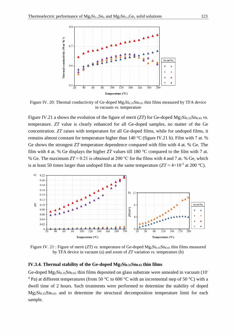
Thermoelectric performance of Mg2Si1-xSnx and Mg2Sn1-xGex solid solutions 123
Figure IV. 20: Thermal conductivity of Ge-doped Mg2Si0.35Sn0.65 thin films measured by TFA device
in vacuum vs. temperature
Figure IV.21 a shows the evolution of the figure of merit (ZT) for Ge-doped Mg2Si0.35Sn0.65 vs.
temperature. ZT value is clearly enhanced for all Ge-doped samples, no matter of the Ge
concentration. ZT raises with temperature for all Ge-doped films, while for undoped films, it
remains almost constant for temperature higher than 140 °C (figure IV.21 b). Film with 7 at. %
Ge shows the strongest ZT temperature dependence compared with film with 4 at. % Ge. The
film with 4 at. % Ge displays the higher ZT values till 180 °C compared to the film with 7 at.
% Ge. The maximum ZT ≈ 0.21 is obtained at 200 °C for the films with 4 and 7 at. % Ge, which
is at least 50 times larger than undoped film at the same temperature (ZT ≈ 4×10⁻³ at 200 °C).
Figure IV. 21 : Figure of merit (ZT) vs. temperature of Ge-doped Mg2Si0.35Sn0.65 thin films measured
by TFA device in vacuum (a) and zoom of ZT variation vs. temperature (b)
IV.3.4. Thermal stability of the Ge-doped Mg2Si0.35Sn0.65 thin films
Ge-doped Mg2Si0.35Sn0.65 thin films deposited on glass substrate were annealed in vacuum (10-
4 Pa) at different temperatures (from 50 °C to 600 °C with an incremental step of 50 °C) with a
dwell time of 2 hours. Such treatments were performed to determine the stability of doped
Mg2Si0.35Sn0.65 and to determine the structural decomposition temperature limit for each
sample.

Thermoelectric performance of Mg2Si1-xSnx and Mg2Sn1-xGex solid solutions 124
As shown in figure IV.22, until 550 °C, the face centered cubic structure (jcpds: 01-089-4254)
remains stable without any secondary phase for doped films with 1 at. % and 4 at. % of Ge
while for doped film with 7 at. % of Ge (figure IV.22) and for undoped film of Mg2Si0.35Sn0.65
at 550 °C, the fcc structure decomposition starts (see figure IV.12 b). At 600 °C, the cubic
Mg2Si0.4Sn0.6 structure vanishes for all samples and decomposition of Ge doped Mg2Si0.35Sn0.65
phase occurs which s leads to Mg, Si, Sn and Ge formation. The (200) diffracted signal related
to Sn (bct) phase (jcpds: 03-065-0296) coexists with (110) diffracted peak of Mg related to
(bcc) phase (jcpds: 03-065-0296) and (002) diffracted signal related to Si (based-centered
orthorhombic) phase (jcpds: 01-089-9054). The (220) diffracted peak related to Ge (fcc) phase
(jcpds: 03-065-9209) is also observed.
Figure IV. 22: X-ray diffraction patterns of the Ge-doped Mg2Si0.35Sn0.65 thin films deposited on glass
substrate and post annealed in vacuum (10-4 Pa) for 2 h at different temperatures. Doped with: a) 1 at.
% Ge, b) 4 at. % Ge, and c) 7 at. % Ge
IV.4. Mg2Ge1-xSnx thin films
Mg2Ge1-xSnx (x= 0, 0.5, 0.7) thin films were deposited by magnetron co-sputtering of Mg, Ge
and Sn targets in an argon atmosphere and the results are compared with Mg2Sn sample. The
power was fixed at 42 W for Mg target, 20 W for Sn target and was systematically changed on
Ge target from 6 to 17 W to tune the coating composition. The Mg and Sn targets were powered
by pulsed direct current (DC) power supplies (Pinnacle, Advanced Energy), while the Ge target
was powered by (DC) power supply (MDX 500, Advanced Energy). The main sputtering
parameters are summarized in Table IV.6.

Thermoelectric performance of Mg2Si1-xSnx and Mg2Sn1-xGex solid solutions 125
Table IV. 6 : Sputtering parameters used during deposition of Mg2Ge1-xSnx coatings.
Ar flow rate (sccm) 50 Target Mg Sn Ge
Working pressure (Pa) 0.41 Discharge power (W) 50 20 6→17
Draw distance (DT-S) (mm) 60 Frequency (kHz) 50 50 0
Run duration (min) 25 𝑻𝒐𝒇𝒇 (µs) 4 4 0
Table IV.7 shows the chemical composition and thickness of coatings measured by EDS
analyses and profilometer, respectively. Three different zones of each coating deposited on
quartz were selected for EDS measurements and the average concentration was calculated. It
can be noted that EDS analyses show relatively homogeneous composition on the entire surface
of deposited thin films.
Table IV. 7 : Composition and thickness of Mg2Ge1-xSnx thin films
Sample no. Mg content
(at. %)
Ge content
(at. %)
Sn content
(at. %)
Nominal
composition
Thickness(µm)
(±20 nm)
Sample # 1 67 ± 1 33 ± 0.5 0 Mg2Ge 0.42
Sample # 2 67 ± 1 16 ± 0.5 17 ± 0.5 Mg2Ge0.5Sn0.5 0.60
Sample # 3 67 ± 1 11 ± 0.5 22 ± 0.5 Mg2Ge0.3Sn0.7 0.77
Sample # 4* 67 ± 1 0 33 ± 0.5 Mg2Sn 1.0
* The results of Sample # 4 is repeated from chapter III, in the aim of a better comprehension of the
effect of Ge substitution in Mg2Ge1-xSnx solid solutions.
For the antifluorite structure of Mg2Sn and Mg2Ge, the band gap energy is about 0.35 eV and
0.74 eV, respectively. The bandgap energy highly depends on the composition in Mg2Ge1-xSnx
solid solution. Based on the first principal calculation and experimental results, the bandgap of
Mg2Ge1-xSnx decreases by increasing the x value [Jiang et al, 2013; Yuan et al., 2019]. The
optical bandgap energy for Mg2Ge1-xSnx was measured by the Kubelka-Munk method. The
bandgap of Mg2Ge is 0.85 eV, while Mg2Ge is not crystallized and exhibits an amorphous
structure. For the Mg2Ge0.3Sn0.7 film, the bandgap is 0.84 eV, which is higher than reported
value in the litritures. For Mg2Ge0.5Sn0.5 thin film, the bandgap is about 0.67 eV, which is in
good agreement with literature [Ryu et al., 2019].
IV.4.1 Structural characterization and thermal stability of the Mg2Ge1-xSnx thin films
Mg2Ge1-xSnx thin films deposited on glass substrate were annealed in vacuum (10-4 Pa) at
different temperatures (from 50 °C to 600 °C with an incremental step of 50 °C) with a dwell
time of 2 hours (figure IV.23 (a-d)). Such treatments were performed to determine the stability
and structural decomposition limit for each sample.
X-ray diffraction patterns of as-deposited Mg2Ge on glass substrate and annealed Mg2Ge in
vacuum (10-4 Pa) at different temperatures is presented in figure IV.23 (a). As deposited Mg2Ge
film is amorphous and such annealing treatments were performed to determine at which
temperature the Mg2Ge starts to crystallize and until which temperature it remains stable. Until
100 °C, the Mg2Ge has an amorphous state. The film crystallizes at 150 °C and diffracted peaks
are observed indicating the formation of the fcc Mg2Ge compound (jcpds: 01-086-1028). From
150 °C to 350 °C, the FWHM and peak intensity increases for Mg2Ge film with raising the
annealing temperature which indicates improvement of crystallinity. For this range of

Thermoelectric performance of Mg2Si1-xSnx and Mg2Sn1-xGex solid solutions 126
temperatures, a strong preferred orientation along (111) crystal plane can be observed. For
temperatures in-between 400-550 °C, the (200) diffraction signal appears but the (111) ones
always remains as a preferential orientated plane. At 600 °C, the preferential orientation is
changed from (111) to (200) crystal plane. It is worth to note that the Mg2Ge film with an
antifluorite structure (space group: 𝐹𝑚3𝑚) and face-centered cubic (fcc) lattice has usually a
preferred orientation along (200) plane [Chuang et al., 2012]. Figure IV.23 (b-c) illustrate te X-
ray diffraction patterns of the Mg2Ge0.5Sn0.5 and Mg2Ge0.3Sn0.7 thin films deposited on glass
substrate and post annealed in vacuum (10-4 Pa) for 2 h at different temperatures. Until 250 °C,
only the main peaks for Mg2Ge1-xSnx solid solutions are observed. For the temperature in-
between 300-500 °C, the main peaks of Mg2Ge1-xSnx solid solutions coexist with (200) and
(101) diffracted peaks related to Sn (bct) phase (jcpds: 03-065-0296). After annealing at 550
°C, Mg2Ge1-xSnx structure vanishes and decomposition phase occurs which leads to Mg, Sn and
Ge formation. The (200) diffracted signal related to Sn phase coexists with (110) diffracted
peak of Mg phase (jcpds: 03-065-0296), and (111) diffracted peak of Ge (jcpds: 03-065-9209).
Figure IV.23 (d) shows the XRD patterns of the Mg2Sn after annealing treatments up to 600 °C
in vacuum. Until 500 °C, the fcc structure (jcpds 03-065-2997) remains. For temperatures
higher than 500 °C, the cubic Mg2Sn structure vanishes and decomposition of Mg2Sn phase
occurs, which leads to Mg and Sn formation. The (200) diffracted signal related to Sn phase
(jcpds 03-065-0296) coexists with (100) and (110) diffracted peaks of Mg phase, respectively.
Figure IV. 23: X-ray diffraction patterns of as deposited Mg2Ge1-xSnx on glass substrate and post
annealed in vacuum (10-4 Pa) for 2 h at different temperatures. a) Mg2Ge, b) Mg2Ge0.5Sn0.5, c)
Mg2Ge0.3Sn0.7, and d) Mg2Sn.

Thermoelectric performance of Mg2Si1-xSnx and Mg2Sn1-xGex solid solutions 127
Figure IV.24 illustrates X-ray diffraction patterns of as-deposited Mg2Ge1-xSnx, which indicates
that the main peaks of all coatings correspond to the cubic antifluorite structure (space group:
𝐹𝑚3𝑚), CaF2-type. Since for both Mg2Ge0.5Sn0.5 and Mg2Ge0.3Sn0.7 solid solutions are formed
because the main peaks of Mg2Ge1-xSnx are situated between peaks of Mg2Ge and Mg2Sn.
Figure IV. 24 : X-ray diffraction patterns for thin films of Mg2Ge1-xSnx.
IV.4.2 Morphological characterization of Mg2Ge1-xSnx thin films
Figure IV.25 reveals top surface morphology and brittle fracture cross section observations of
thin films deposited on glass substrates by SEM. The granular morphology with some porosities
and open spaces can be seen for Mg2Sn. By increasing the Ge content, the morphology becomes
more compact. The smooth surface with granular features is observed for the Mg2Ge0.3Sn0.7
film. Mg2Ge0.5Sn0.5 reveals the smooth surface with cone-like features. For Mg2Ge the smooth
surface with granular features is viewed. The morphology becomes more compact for this
sample.
Brittle fracture cross-section observations show a relatively columnar morphology with some
open spaces for Mg2Sn. For Mg2Ge0.3Sn0.7, the morphology becomes more compact with a
dense feature. Mg2Ge0.5Sn0.5 film exhibits a dense and slightly columnar structure. Mg2Ge
reveals a glassy like morphology and the film becomes denser and more compact. By increasing
the Ge content in the films, the thickness of the film decreases. All samples perfectly cover the
surface of the substrate and no cracks and delamination were detected on the top surface of the
films. A good adhesion between films and substrate is also observed. The film thickness
measured by SEM is relatively homogeneous for all samples.

Thermoelectric performance of Mg2Si1-xSnx and Mg2Sn1-xGex solid solutions 128
Figure IV. 25: SEM micrographs of films deposited on glass substrate (a-d) and SEM cross section
micrographs (e-h) of Mg2Ge1-xSnx with different compositions.
IV.4.3. Measurement of electronic transport properties of Mg2Ge1-xSnx thin films
The electronic transport properties of Mg2Ge1-xSnx thin films vs. temperature were measured in
air by Hall effect. The electronic properties of the Mg2Ge film were measured for as deposited
(amorphous film) and after 2 hours annealing in vacuum at 400 °C (crystallized film), in order
to compare the results of amorphous and crystallized films. As the improved crystallinity in the
film leads to a reduction of crystal defects (like dislocations), so such a change in defect could
strongly affect the electronic transport properties of the films [Chuang et al., 2012]. Figure
IV.26 shows the temperature dependency of DC electrical conductivity for Mg2Ge1-xSnx thin
films. For all samples the electrical conductivity is enhanced by temperature indicating typical
behavior of semiconductors [Liu et al., 2013]. Amorphous Mg2Ge exhibits the lowest electrical
conductivity throughout the investigated temperature range, while after annealing at 400 °C the
electrical conductivity is improved for this sample. The electrical conductivity for crystallized
Mg2Ge is about 2.5 times higher than amorphous Mg2Ge at 200 °C. It is right to note that, slope
change happened for amorphous Mg2Ge electrical conductivity curve vs. temperature at about
120 °C. It can be related to the beginning of the film crystallization as reported in figure IV.23
(a). The highest electrical conductivity throughout the investigated temperature range was

Thermoelectric performance of Mg2Si1-xSnx and Mg2Sn1-xGex solid solutions 129
obtained for Mg2Ge0.3Sn0.7 with maximum value of about 1.76×10⁴ Sm-1 at 200 °C.
Mg2Ge0.5Sn0.5 shows higher electrical conductivity at temperature below 130 °C compare to
Mg2Sn. For a temperature higher than 130°C, both samples exhibit relatively the same electrical
conductivity.
Figure IV. 26: DC electrical conductivity of Mg2Ge1-xSnx thin films vs. temperature
Figure IV.27 presents the variation of carrier concentration vs. temperature for the Mg2Ge1-xSnx
films. The carrier concentration increases with a sharp slope as the temperature rises for
amorphous Mg2Ge. This sample shows the lowest carrier concentration for the temperature
below 120 °C because of its amorphous state but at higher than 120 °C, the film crystallization
process started, and the carrier concentration can reach the same order of magnitude to that of
the crystallized Mg2Ge film. The carrier concentration raises linearly with the temperature for
all crystallized films. It is important to highlight that Mg2Sn thin film presents higher carrier
concentration than Mg2Ge while in solid solution films carrier concentration increases with Ge
content. Mg2Ge0.5Sn0.5 thin film shows the highest carrier concentration throughout the
measured temperature range. The value reaches 3.2×1026 m-3 at 200 °C for this sample.
Figure IV. 27: Carrier concentration of Mg2Ge1-xSnx thin films vs. temperature
The variation of carrier mobility vs. temperature for the Mg2Ge1-xSnx films is shown in figure
IV.28. For all samples except as deposited Mg2Ge, the Hall mobility almost follows the form
µ~𝑇0, corresponding to a neutral impurity scattering mechanism. For as deposited Mg2Ge, the

Thermoelectric performance of Mg2Si1-xSnx and Mg2Sn1-xGex solid solutions 130
Hall mobility obeys the form µ~𝑇−3/2, indicating acoustical phonon is the dominating
scattering mechanism for this sample because of its amorphous state [Bashir et al., 2014; Chen
et al., 2015; Mao et al., 2018]. The well-crystallized Mg2Ge shows higher carrier mobility
compare with amorphous layer, which is in good agreement with literature [Chuang et al.,
2012]. The Hall coefficient is positive for both as deposited and well-crystallized Mg2Ge, which
indicte p-type conduction.The Mg2Sn exhibits the highest carrier mobility throughout the
measured temperature. The film carrier mobility decrease, while the Ge content in the film raise
for Mg2Ge1-xSnx solid solution compounds. The Mg2Ge1-xSnx films present higher carrier
mobility compare to the Mg2Si1-xSnx thin films (see section IV.2.2; figure IV.6). It is also worth
to note that the Mg2Ge1-xSnx films show lower carrier mobility compare to the Ge-doped
Mg2Si0.35Sn0.65 thin films (see section IV.3.2; figure IV.17).
Figure IV. 28: Carrier mobility vs. temperature of Mg2Ge1-xSnx thin films.
IV.4.4. Measurement of thermoelectric properties of Mg2Ge1-xSnx thin films
The thermoelectric properties were measured in vacuum (about 10-4 Pa) at different
temperatures using the TFA device on Linseis chips covered by Mg2Ge1-xSnx thin films. As
previously noted in section II.4.6.6, after inserting the chip in TFA device, the correct
installation of the chip and resistance homogeneity of deposited film on chip are tested in order
to obtain accurate results after measurements. The chip covered by Mg2Ge was failed in both
tests because of high film resistivity with its amorphous state, and the Mg2Ge crystallized film
on Linseis chip was broken during annealing treatment because of the stress relaxation during
annealing process.
Figures IV.29 illustrates the evolution of the electrical conductivity for Mg2Ge1-xSnx vs.
temperature in vacuum. The positive evolution of electrical conductivity with temperature is
observed for all films. Mg2Sn exhibits the lowest electrical conductivity over the whole
investigated temperature range. The electrical conductivity is improved by formation of
Mg2Ge1-xSnx solid solutions. The highest electrical conductivity of about 2.4×10⁴ S m-1 at 200
°C was obtained for Mg2Ge0.3Sn0.7 thin film.

Thermoelectric performance of Mg2Si1-xSnx and Mg2Sn1-xGex solid solutions 131
Figure IV. 29: Electrical resistivity vs. temperature of Mg2Ge1-xSnx thin films measured by TFA device
under vacuum.
Figure IV.30 shows the Seebeck coefficient for Mg2Ge1-xSnx thin films as a function of the
temperature. All samples exhibit a p-type semiconducting behavior since the Seebeck
coefficient is positive throughout the temperature range. Mg2Sn has the highest Seebeck
coefficient value about 174 µV K-1 at 30 °C. The Seebeck coefficient decreases with
temperature and reaches 122 µV K-1at 200 °C. For Mg2Ge0.5Sn0.5 and Mg2Ge0.3Sn0.7 films, the
Seebeck coefficient is enhanced with the temperature, and reaches 180 and 148 µV K-1 at 200
°C, respectively.
Figure IV. 30 : Seebeck coefficient vs. temperature of Mg2Ge1-xSnx thin films measured by TFA
device in vacuum.
Figure IV.31 reveals the variation of thermal conductivity vs. temperature for Mg2Ge1-xSnx thin
films measured by TFA device. Thermal conductivity decreases drastically by formation of
Mg2Ge1-xSnx solid solutions due to effect of alloying on their lattice thermal conductivity. The
mass difference scattering is the main mechanism for decreasing the lattice thermal
conductivity. Therefore, the mass difference between Ge (72.6 a.m.u) and Sn (118.71 a.m.u)
leads to the reduction of thermal conductivity [Bashir et al., 2014]. Compare with Mg2Si1-xSnx
(figure IV.10) and Ge-doped Mg2Si0.35Sn0.65 (figure IV.20), the thermal conductivity is higher
for Mg2Ge1-xSnx films. The mass difference between Si and Sn is huger in Mg2Si1-xSnx, and in
the case of Ge-doped Mg2Si0.35Sn0.65, the phonon scattering is enhanced by various precipitates

Thermoelectric performance of Mg2Si1-xSnx and Mg2Sn1-xGex solid solutions 132
[Bashir et al., 2014; Yuan et al., 2019]. The thermal conductivity increases with the temperature
for the Mg2Sn. The Mg2Sn exhibits the highest thermal conductivity of about 1.7 W m-1 K-1 at
200 °C. The thermal conductivity first increases till 140 °C and reaches a maximum value of
1.08 W m-1 K-1 for Mg2Ge0.3Sn0.7, and then decreases. The thermal conductivity remains quite
constant by the temperature for Mg2Ge0.5Sn0.5. This sample shows the lowest thermal
conductivity throughout the investigated temperature range and does not go over 0.73 Wm-1 K-
1.
Figure IV. 31 : Thermal conductivity vs. temperature of Mg2Ge1-xSnx thin films measured by TFA
device in vacuum.
The variation of figure of merit ZT for Mg2Ge1-xSnx vs. temperature is shown in figure IV.32.
The ZT is improved by the formation of Mg2Ge1-xSnx solid solutions. The evolution of ZT vs.
temperature is positive for all samples. The highest ZT~ 0.26 at 200 °C is obtained for the
Mg2Ge0.3Sn0.7, which is at least 6 times higher than ZT obtained for Mg2Sn at the same
temperature.
Figure IV. 32: Figure of merit (ZT) vs. temperature of Mg2Ge1-xSnx thin films measured by TFA
device in vacuum.

Thermoelectric performance of Mg2Si1-xSnx and Mg2Sn1-xGex solid solutions 133
IV.5. Conclusion
In the first part, Mg2Si1-xSnx solid solutions were deposited by magnetron co-sputtering of Mg,
Si and Sn targets in an argon atmosphere. All films adopted the stable face-centered cubic
structure. The influence of chemical composition on the electronic transport properties of
Mg2Si1-xSnx thin films was studied in the range of temperatures: 30-200 °C. Hall effect
measurements led to conclude that electrical conductivity is ruled by the carrier concentration
rather than carrier mobility in these samples. The thermoelectric properties of Mg2Si1-xSnx were
investigated in the range of temperatures: 30-200 °C. The Mg2Si0.3Sn0.7 and Mg2Si0.35Sn0.6 are
p-type semiconductors as the Seebeck coefficient is positive all over the measured temperature
range, while Mg2Si0.7Sn0.3 shows an n-type conduction. Thermal conductivity decreases
drastically due to the formation of Mg2Si1-xSnx solid solutions. This is assigned to the effect of
alloying on their lattice thermal conductivity. For Mg2Si0.7Sn0.3 thin film, thermal conductivity
is enhanced till 130 °C and then decreased drastically. This sample has the lowest thermal
conductivity of about 0.37 W m-1 K-1 at 30 °C, and it reaches 0.57 W m-1 K-1 at 200 °C. The
highest ZT ~ 3.6 × 10⁻² at 200 °C is obtained for n-type Mg2Si0.7Sn0.3 compound. For the p-type
Mg2Si0.35Sn0.65, ZT = 4×10⁻³ at 200 °C. Films deposited on glass substrate were annealed in
vacuum (10-4 Pa) at different temperatures to determine their thermal stability. Till 500 °C, the
face centered cubic structure (jcpds 01-089-4254) remains stable. At 600 °C, the cubic
Mg2Si0.4Sn0.6 structure vanishes and decomposition of Mg2Si1-xSnx phase occurs, which leads
to Mg, Si and Sn formation.
In the second part, the p-type Mg2Si0.35Sn0.65 is selected for doping with Ge, to enhance
thermoelectric properties of the films. Ge-doped (0, 1, 4, and 7 at. %) Mg2Si0.35Sn0.65 thin films
were deposited. The stable face-centered cubic structure was observed for all films. The
influence of Ge-doping on the thermoelectric properties of Mg2Si0.35Sn0.65 was studied in the
range of temperatures: 30-200 °C. By Ge-doping electrical conductivity and Seebeck
coefficient were both enhanced, which led to an improvement of thermoelectric performances
of thin films. The influence of carrier scattering mechanism on lattice thermal conductivity was
discussed. The results showed that a lower thermal conductivity was expected while the
acoustical phonon scattering mechanism prevails for the sample doped with 7 at. % Ge. The
film with 4 at. % Ge displayed the highest ZT values till 180 °C compared to other films and
finally the maximum ZT ~ 0.21 was reached at 200 °C for the films doped with 4 and 7 at. %
Ge. Ge-doped Mg2Si0.35Sn0.65 thin films deposited on glass substrate were annealed in vacuum
to determine the thermal stability of Mg2Si0.35Sn0.65 after Ge-doping. Until 550 °C, the face-
centered cubic structure (jcpds: 01-089-4254) is kept and at 600 °C, the cubic Mg2Si0.4Sn0.6
structure vanishes. Structure decomposition occurs, which leads to Mg, Si, Sn and Ge
formation. This group shows the highest thermal stability among the other studied samples in
this work.
In the last part, Mg2Ge1-xSnx (x= 0, 0.5, 0.7) thin films were deposited by magnetron co-
sputtering of Mg, Ge and Sn targets in an argon atmosphere. The results were compared with
Mg2Sn sample. Mg2Ge1-xSnx films adopts the cubic antifluorite (space group: 𝐹𝑚3𝑚), CaF2-
type. Mg2Ge0.5Sn0.5 and Mg2Ge0.3Sn0.7 solid solutions are situated between Mg2Ge and Mg2Sn.

Thermoelectric performance of Mg2Si1-xSnx and Mg2Sn1-xGex solid solutions 134
The thermal stability of the Mg2Ge1-xSnx was examined after annealing in vacuum at different
temperatures. Until 250 °C, only the main peaks for Mg2Ge1-xSnx solid solutions are observed.
For the temperature in-between 300-500 °C, the main peaks of Mg2Ge1-xSnx solid solutions
coexist with body-centered tetragonal Sn phase. From 550 °C, Mg2Ge1-xSnx structure vanishes
and decomposition phase occurs, which leads to Mg, Sn and Ge formation. Mg2Ge as deposited
was amorphous. Therefore, Mg2Ge on glass substrate was annealed in vacuum at different
temperatures to determine at which temperature the Mg2Ge starts to crystallize. The film
crystallization started at higher than 100 °C with formation of face-centered cubic Mg2Ge phase
(jcpds: 01-086-1028). The diffraction intensity increased with raising the annealing
temperature, which indicates improving crystallinity and texturing of the film. The influence of
chemical composition and structure on the films electronic transport was discussed. For all
samples except non-crystallized Mg2Ge, the Hall mobility almost follows the form µ~𝑇0,
corresponding to a neutral impurity scattering mechanism. For amorphous Mg2Ge, the Hall
mobility obeys the form µ~𝑇−3/2 , indicating acoustical phonon scattering mechanism for this
sample. The thermoelectric properties were investigated only for Mg2Ge1-xSnx thin films as
Mg2Ge, was failed in pre-measurement tests of TFA device. The results were compared with
Mg2Sn thin film. Mg2Ge1-xSnx is a p-type semiconductor due to the positive sign of Seebeck
coefficient. Thermal conductivity decreases drastically by formation of Mg2Ge1-xSnx solid
solutions compare to Mg2Sn due to the effect of alloying on their lattice thermal conductivity.
The highest ZT~ 0.26 at 200 °C was obtained for the Mg2Ge0.3Sn0.7, which was at least 6 times
higher than ZT obtained for Mg2Sn films at the same temperature.

Thermoelectric performance of Mg2Si1-xSnx and Mg2Sn1-xGex solid solutions 135
IV.6. References An, T. H., Park, C., Seo, W. S., Choi, S. M., Kim, I. H., & Kim, S. U. (2012). Enhancement of
p-type thermoelectric properties in an Mg2Sn system. Journal of Korean Physical Society, 60,
1717-1723.
Bashir, M. B. A., Mohd Said, S., Sabri, M. F. M., Shnawah, D. A., & Elsheikh, M. H. (2014).
Recent advances on Mg2Si1-xSnx materials for thermoelectric generation. Renewable and
Sustainable Energy Reviews, 37, 569-584.
Chen, S. Zhang, X., Fan, W., Yi, T., Quach, D. V., Bux, S., Meng, Q., Kauzlarich, S. M., &
Munir, Z. A. (2015). One-step low temperature reactive consolidation of high purity
nanocrystalline Mg2Si. Journal of Alloys and Compounds, 625, 251-257.
Chuang, L., Wang, D. Y., Tan, T. T., Assadi, M. H. N., & Li, S. (2012). Processing dependence
of structural and physical properties of Mg2Ge thin films prepared by pulsed laser deposition.
Thin Solid Films, 520, 6226-6229.
Gao, H. L., Liu, X. X., Zhu, T. J., Yang, S. H., & Zhao, X. B. (2011). Effect of Sb doping on
the thermoelectric properties of Mg2Si0.7Sn0.3 solid solutions. Journal of Electronic Materials
40, 830-834.
Gao, H., Zhu, T., Liu, X., Chen, L., & Zhao, X. (2011). Flux synthesis and thermoelectric
properties of eco-friendly Sb doped Mg2Si0.5Sn0.5 solid solutions for energy harvesting. Journal
of Materials Chemistry, 21, 5933-5937.
Jiang, G., Chen, L., He, J., Gao, H., Du, Z., Zhao, X., Tritt, T. M., & Zhu, T. (2013). Improving
p-type thermoelectric performance of Mg2(Ge, Sn) compounds via solid solution and Ag
doping. Intermetallics, 32, 312-317.
Kamila, H., Sankhla, A., Yasseri, M., Hoang, N. P., Farahi, N., Mueller, E., & de Boor, J.
(2019). Synthesis of p-type Mg2Si1-xSnx with x= 0-1 and optimization of the synthesis
parameters. Materials Today: Proceeding, 8, 546-555.
Kanatzidis, M. G. (2010). Nanostructured thermoelectrics: The new paradigm?. Chemistry of
Materials, 22, 648-659.
Khan, A. U., Vlachos, N., & Kyratsi, T. (2013). High thermoelectric figure of merit of Mg2Si
0.55Sn0.4Ge0.05 materials doped with Bi and Sb. Scripta Materialia, 69, 606-609.
Le-Quoc, H., Lacoste, A., Béchu, S., Bès, A., Bourgault, D., & Fruchart, D. (2012). Deposition
of thin films of Mg2Si1-xSnx solid solution by plasma-assisted co-sputtering. Journal of Alloys
and Compounds, 538, 73-78.
Liu, W., Tan, X., Yin, K., Liu, H., Tang, X., Shi, J., Zhang, Q., & Uher, C. (2012). Convergence
of conduction bands as a means of enhancing thermoelectric performance of n-type Mg2Si1-
xSnx solid solutions. Physical Review Letters, 108, 166601-166606.
Liu, W., Yin, K., Su, X., Li, H., Yan, Y., Tang, X., & Uher, C. (2013). Enhanced hole
concentration through Ga doping and excess of Mg and thermoelectric properties of p-type
Mg2(1+z)(Si0.3Sn0.7)1-yGay” Intermetallics, 32, 352-361.

Thermoelectric performance of Mg2Si1-xSnx and Mg2Sn1-xGex solid solutions 136
Mao, J., Liu, Z., Zhou, J., Zhu, H., Zhang, Q., Chen, G., & Ren, Z. (2018). Advances in
thermoelectrics. Advances in Physics, 67, 69-147.
Ryu, B., Park, S., Choi, E. A., Boor, J. D., Ziolkowski, P., Chung, J., & Park, S. D. (2019).
Hybrid-functional and quasi-particle calculation of band structures of Mg2Si, Mg2Ge, and
Mg2Sn. Korean Physical Society, 75, 144-152.
Santos, R., Aminorroaya Yamini, S., & Dou, S. X. (2018). Recent progress in magnesium-
based thermoelectric materials. Journal of Materials Chemistry A, 6, 3328-3341.
Satyala, N., & Vashaee, D. (2012). The effect of crystallite size on the thermoelectric properties
of bulk nanostructured magnesium silicide (Mg2Si) compounds. Applied Physics Letters, 100,
073107-1-073107-4.
Vineis, C. J., Shakouri, A., Majumdar, A., & Kanatzidis, M. G. (2010). Nanostructured
thermoelectrics: Big efficiency gains from small features. Advanced Materials, 22, 3970-3980.
Yuan, G., Han, S., Lei, X., Hu, J., Liu, W., Wang, Q., Chen, C., Zhang, Q., Zhang, Q., & Gu,
M. (2019). The enhancement of thermoelectric performance of p-type Li doped Mg2Ge0.4Sn0.6
by si addition. Scripta Materialia, 166, 122-127.
Zaitsev, N. K., Fedorov, M. I., Gurieva, E. A., Eremin, I. S., Konstantinov, P. P., Samunin, A.
Y., & Vedernikov, M. V. (2006). Highly effective Mg2Si1-xSnx thermoelectrics. Physical
Review B, 74, 045207-1-045207-5.

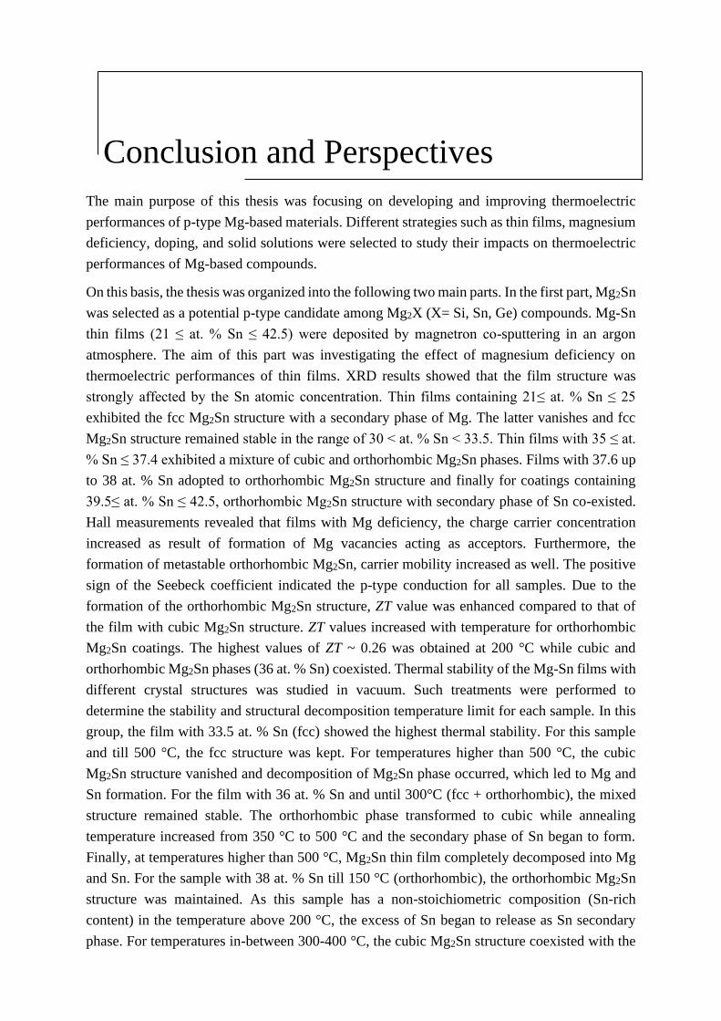
Conclusion and Perspectives
The main purpose of this thesis was focusing on developing and improving thermoelectric
performances of p-type Mg-based materials. Different strategies such as thin films, magnesium
deficiency, doping, and solid solutions were selected to study their impacts on thermoelectric
performances of Mg-based compounds.
On this basis, the thesis was organized into the following two main parts. In the first part, Mg2Sn
was selected as a potential p-type candidate among Mg2X (X= Si, Sn, Ge) compounds. Mg-Sn
thin films (21 ≤ at. % Sn ≤ 42.5) were deposited by magnetron co-sputtering in an argon
atmosphere. The aim of this part was investigating the effect of magnesium deficiency on
thermoelectric performances of thin films. XRD results showed that the film structure was
strongly affected by the Sn atomic concentration. Thin films containing 21≤ at. % Sn ≤ 25
exhibited the fcc Mg2Sn structure with a secondary phase of Mg. The latter vanishes and fcc
Mg2Sn structure remained stable in the range of 30 ˂ at. % Sn < 33.5. Thin films with 35 ≤ at.
% Sn ≤ 37.4 exhibited a mixture of cubic and orthorhombic Mg2Sn phases. Films with 37.6 up
to 38 at. % Sn adopted to orthorhombic Mg2Sn structure and finally for coatings containing
39.5≤ at. % Sn ≤ 42.5, orthorhombic Mg2Sn structure with secondary phase of Sn co-existed.
Hall measurements revealed that films with Mg deficiency, the charge carrier concentration
increased as result of formation of Mg vacancies acting as acceptors. Furthermore, the
formation of metastable orthorhombic Mg2Sn, carrier mobility increased as well. The positive
sign of the Seebeck coefficient indicated the p-type conduction for all samples. Due to the
formation of the orthorhombic Mg2Sn structure, ZT value was enhanced compared to that of
the film with cubic Mg2Sn structure. ZT values increased with temperature for orthorhombic
Mg2Sn coatings. The highest values of ZT ~ 0.26 was obtained at 200 °C while cubic and
orthorhombic Mg2Sn phases (36 at. % Sn) coexisted. Thermal stability of the Mg-Sn films with
different crystal structures was studied in vacuum. Such treatments were performed to
determine the stability and structural decomposition temperature limit for each sample. In this
group, the film with 33.5 at. % Sn (fcc) showed the highest thermal stability. For this sample
and till 500 °C, the fcc structure was kept. For temperatures higher than 500 °C, the cubic
Mg2Sn structure vanished and decomposition of Mg2Sn phase occurred, which led to Mg and
Sn formation. For the film with 36 at. % Sn and until 300°C (fcc + orthorhombic), the mixed
structure remained stable. The orthorhombic phase transformed to cubic while annealing
temperature increased from 350 °C to 500 °C and the secondary phase of Sn began to form.
Finally, at temperatures higher than 500 °C, Mg2Sn thin film completely decomposed into Mg
and Sn. For the sample with 38 at. % Sn till 150 °C (orthorhombic), the orthorhombic Mg2Sn
structure was maintained. As this sample has a non-stoichiometric composition (Sn-rich
content) in the temperature above 200 °C, the excess of Sn began to release as Sn secondary
phase. For temperatures in-between 300-400 °C, the cubic Mg2Sn structure coexisted with the
Conclusions and Perspectives 139
metastable orthorhombic Mg2Sn phase and Sn secondary phase, respectively. For temperatures
450-500 °C, the cubic Mg2Sn structure coexisted with the metastable orthorhombic Mg2Sn
phase and body centered tetragonal Sn phase. For temperatures higher than 550 °C, the cubic
and orthorhombic Mg2Sn structures vanished and decomposition of Mg2Sn phase led to Mg
and Sn formation.
In order to investigate the effect of Mg-deficiency and Cu-doping on thermoelectric properties
of Mg-Sn, two groups of Mg-Sn thin films were deposited by magnetron co-sputtering of Mg,
Sn and Cu targets in an argon atmosphere. Group I with ⌈𝑀𝑔⌉
[𝑆𝑛]= 2 and group II with
⌈𝑀𝑔⌉
[𝑆𝑛]= 1.75
were doped by different Cu concentrations (0, 0.5 and 1.5 at. %). Only the film of group I with
0 at. % Cu showed a stable fcc structure. For other samples of both groups, a mixture of fcc and
metastable orthorhombic phases coexisted. Thermoelectric properties of both groups were
measured in the temperature range 30-200 °C to investigate the influence of Cu-doping. It was
shown that the Cu introduction in stoichiometric Mg2Sn compound improved the electronic
properties, but also the thermal conductivity. On the other hand, Cu-doping reduced the Seebeck
coefficient leading to improved thermoelectric properties in a restraint range. The highest ZT ~
0.07 was obtained for films of group I at 200 °C with 0.5 at. % of Cu. Films of group II with a
Mg-deficiency showed a different behavior. They exhibited a higher electrical conductivity due
to a better carrier mobility, with a thermal conductivity and Seebeck coefficient of the same
order of magnitude than in stoichiometric films. As a result, enhanced thermoelectric properties,
almost 4 times higher (ZT = 0.27 at 200 °C with 0.5 at. % of Cu) were produced by means of
Mg-deficiency and Cu-doping of Mg2Sn thin films sputter-deposited. It is believed that the
mixture of cubic and orthorhombic phases contributed to the achievement of a higher carrier
mobility and better thermoelectric properties. These results proved the Mg-deficiency is more
effective strategy to improve thermoelectric performances rather than Cu-doping.
In the next part, the influence of the structural modification of Mg2X (X= Si, Sn, Ge) by solid
solutions formation was studied The solid solution features make changes in the crystal lattice
(i.e., disorder) which produces strong phonon scattering centers and reduce thermal
conductivity. Mg2Si1-xSnx solid solutions were deposited by magnetron co-sputtering of Mg, Si
and Sn targets in an argon atmosphere. All films adopted the stable fcc structure. The influence
of chemical composition on the electronic transport properties of Mg2Si1-xSnx thin films was
explored. Hall effect measurements led to conclude that electrical conductivity is ruled by
carrier concentration rather than carrier mobility in these samples. The thermoelectric
properties of Mg2Si1-xSnx were investigated by means of TFA. The Mg2Si0.3Sn0.7 and
Mg2Si0.35Sn0.65 exhibited a p-type behavior with a positive Seebeck coefficient throughout the
measured temperature range, while Mg2Si0.7Sn0.3 showed n-type conduction. Thermal
conductivity decreased drastically by formation of Mg2Si1-xSnx solid solutions due to effect of
alloying on their lattice thermal conductivity. The highest ZT ~ 3.6 × 10⁻² at 200 °C was obtained
for n-type Mg2Si0.7Sn0.3 compound. For the p-type Mg2Si0.35Sn0.65, ZT reached 4 × 10⁻³ at 200
°C. Films were annealed in vacuum (10-4 Pa) at different temperatures to determine their
stability and structural decomposition temperature limit. Till 500 °C, the fcc structure remained

Conclusions and Perspectives 140
stable. At 600 °C, the cubic Mg2Si0.4Sn0.6 structure vanished and decomposition of Mg2Si1-xSnx
phase occurred, which led to Mg, Si and Sn formation.
Ge-doped (0, 1, 4, and 7 at. %) Mg2Si0.35Sn0.65 thin films were deposited by magnetron co-
sputtering of Mg, Si, Sn and Ge targets in an argon atmosphere. The stable fcc structure was
observed for all films. The influence of Ge-doping on the thermoelectric properties of
Mg2Si0.35Sn0.65 was studied. By Ge-doping electrical conductivity and Seebeck coefficient were
both enhanced, which led to an improvement of thermoelectric performances of the films. The
influence of carrier scattering mechanism on lattice thermal conductivity was discussed. The
results showed that a lower thermal conductivity was expected while the acoustical phonon
scattering mechanism dominated for the sample doped with 7 at. % Ge. The film with 4 at. %
Ge displayed the highest ZT values till 180 °C compared to other films and finally the maximum
ZT ~ 0.21 was reached at 200 °C for the films doped with 4 and 7 at. % Ge. Ge-doped
Mg2Si0.35Sn0.65 thin films deposited on glass substrate were annealed in vacuum to determine
the stability Mg2Si0.35Sn0.65 after Ge-doping. Until 550 °C, the fcc structure remained and at
600 °C, the cubic Mg2Si0.4Sn0.6 structure vanished and structure decomposition occurred, which
led to Mg, Si, Sn and Ge formation. This group showed the highest thermal stability among the
other studied samples in this work. Mg2Ge1-xSnx (x= 0, 0.5, 0.7) thin films were deposited by
magnetron co-sputtering of Mg, Ge and Sn targets in an argon atmosphere and the results were
compared with Mg2Sn sample. The structure of Mg2Ge1-xSnx films is a cubic antifluorite (space
group: 𝐹𝑚3𝑚), CaF2-type. Since Mg2Ge0.5Sn0.5 and Mg2Ge0.3Sn0.7 solid solutions mains peaks
are between Mg2Ge and Mg2Sn. The thermal stability of the Mg2Ge1-xSnx was examined after
annealing in vacuum at different temperatures. Until 250 °C, only the main peaks related to
Mg2Ge1-xSnx solid solutions were observed. For temperatures in-between 300-500 °C, the main
peaks of Mg2Ge1-xSnx solid solutions coexisted with Sn secondary phase. From 550 °C,
Mg2Ge1-xSnx structure vanished and decomposition phase occurred, which led to Mg, Sn and
Ge formation. As-deposited Mg2Ge was amorphous. Therefore, Mg2Ge on glass substrate was
annealed in vacuum at different temperatures and the film crystallization started at temperatures
higher than 100 °C with the formation of fcc Mg2Ge. The diffraction intensity increased with
raising the annealing temperature, which indicates an improvement of crystallinity and
texturing of the film. The influence of chemical composition and structure on the films
electronic transport was discussed. The thermoelectric properties were investigated only for
Mg2Ge1-xSnx thin films as Mg2Ge, was failed in pre-measurement tests of TFA device and the
results were compared with Mg2Sn thin film. Mg2Ge1-xSnx exhibited a p-type behavior due to
the positive sign of Seebeck coefficient. Thermal conductivity decreased drastically related to
the formation of Mg2Ge1-xSnx solid solutions compare to Mg2Sn due to effect of alloying on
their lattice thermal conductivity. The highest ZT~ 0.26 at 200 °C was obtained for the
Mg2Ge0.3Sn0.7 which was at least 6 times higher than obtained ZT for Mg2Sn at the same
temperature.
In this work, the results of different strategies for enhancing thermoelectric performance of Mg-
based compounds were discussed. The Mg-deficiency in Mg-Sn system and Ge-doping Mg2Si1-
xSnx solid solutions proved to be the most effective strategy.

Conclusions and Perspectives 141
About the further studies, exploring new p-type dopants such as Ni, Cu, Ag, Zn, or introducing
nano particles as dopant. It is also possible to imagine deposition of Mg2Ge at higher
temperatures by magnetron sputtering, in order to favor crystallized films for measuring
thermoelectric properties by means of TFA. It is also possible to enhance thermoelectric
properties by nanostructuring i.e. Glancing Angle Deposition, or nano multilayer deposition.

Scientific production
Publications:
Thermoelectric performance of Ge-doped Mg2Si0.35Sn0.65 thin films
Safavi, M., Martin, N., Aubry, E., Linseis, V., Billiard, A., & Arab Pour Yazdi, M. (2021).
Journal of Materials Engineering and Performance, accepted.
Impacts of Cu-doping and Mg-deficiency on Mg2Sn thin films thermoelectric
properties
Safavi, M., Martin, N., Aubry, E., Linseis, V., Billiard, A., & Arab Pour Yazdi, M. (2021).
Journal of Electronic Materials, 50, 2738-2749.
Thermoelectric properties improvement in Mg2Sn thin films by structural
modification
Safavi, M., Martin, N., Linseis, V., Palmino, F., Cherioux, F., Billiard, A., & Arab Pour
Yazdi, M. (2019). Journal of Alloys and Compounds, 797, 1078-1085.
Oral presentation:
Impacts of Cu-doping and Mg-deficiency on Mg2Sn thin films thermoelectric properties
M. Safavi, N. Martin, V. Linseis, A. Billard, M. Arab Pour Yazdi, JNTE2019 (La Journée
thématique de thermoélectrique, 20-22 Janvier 2020, Metz-France
Posters:
Impact of Cu doping and Mg-deficient in Mg2Sn thin films thermoelectric properties
M. Safavi, N. Martin, V. Linseis, A. Billard, M. Arab Pour Yazdi, l’école thématique
Thermoélectricité, organisée par le GIS Thermoélectricité, 6 - 11 octobre 2019, La Bresse-
France.
Revêtements de Mg2Sn par pulvérisation cathodique magnétron : de la synthèse aux
propriétés thermoélectriques
M. Safavi, M. Arab Pour Yazdi, N. Martin, V. Linseis, F. Palmino, F. Cherioux, A. Billard
Matériaux 2014, 24-28 novembre 2018, Strasbourg-France.
Mg2Sn thin films prepared by magnetron sputtering: from synthesis to thermoelectric
properties
M. Safavi, N. Martin, V. Linseis, A. Billard, M. Arab Pour Yazdi, FEMTO-ST annual
conference, 26 juin 2018, Besançon-France

3

Copyright © 2022 FDOKUMEN