Transition metal oxides – Thermoelectric properties
95
1 Transition metal oxides- thermoelectric properties Sumeet Walia, a * Sivacarendran Balendhran, a Hussein Nili, a,b Serge Zhuiykov, c Gary Rosengarten, d Qing Hua Wang, e Madhu Bhaskaran, a,b Sharath Sriram, a,b Michael S. Strano e and Kourosh Kalantar-zadeh a * a School of Electrical and Computer Engineering, RMIT University, Melbourne, Australia b Functional Materials and Microsystems Research Group, RMIT University, Melbourne, Australia c Materials Science and Engineering Division, CSIRO, Highett, Victoria, Australia d School of Aerospace, Mechanical and Manufacturing Engineering,RMIT University, Melbourne, Australia e Department of Chemical Engineering, Massachusetts Institute of Technology, Cambridge, Massachusetts, USA. *Corresponding author emails: [email protected], and [email protected] RMIT University, GPO 2476, Melbourne-3000, Victoria, Australia. Ph: + 61-3-9925-3254 Abstract Transition metal oxides (TMOs) are a fascinating class of materials due to their wide rangingelectronic, chemical and mechanical properties. Additionally, they are gaining increasing attention for theirthermoelectric (TE) properties due to their high temperature stability,tunable electronic and phonon transport properties and well established synthesis techniques.In this article, we review TETMOs at cryogenic, ambient and high temperatures. An overview of strategies used for morphological, compostingand stoichiometric tuning of their key TEparametersis presented.Thisarticle also provides an outlook on the current and future prospects of implementing TMOs for a wide range of TE applications. Keywords: transition metal oxides, thermoelectric, Seebeck coefficient, electrical conductivity, thermal conductivity, doping, stoichiometry,compositing, nanostructuring
Transcript of Transition metal oxides – Thermoelectric properties

1
Transition metal oxides- thermoelectric properties
Sumeet Walia,a* Sivacarendran Balendhran,aHussein Nili,a,b Serge Zhuiykov,cGary
Rosengarten,dQing Hua Wang,eMadhu Bhaskaran,a,b Sharath Sriram,a,b Michael S.
Stranoeand Kourosh Kalantar-zadeha*
aSchool of Electrical and Computer Engineering, RMIT University, Melbourne, Australia
b Functional Materials and Microsystems Research Group, RMIT University, Melbourne, Australia
cMaterials Science and Engineering Division, CSIRO, Highett, Victoria, Australia
dSchool of Aerospace, Mechanical and Manufacturing Engineering,RMIT University, Melbourne, Australia
eDepartment of Chemical Engineering, Massachusetts Institute of Technology, Cambridge, Massachusetts,
USA.
*Corresponding author emails:[email protected],and [email protected]
RMIT University, GPO 2476, Melbourne-3000, Victoria, Australia.
Ph: + 61-3-9925-3254
Abstract
Transition metal oxides (TMOs) are a fascinating class of materials due to their wide
rangingelectronic, chemical and mechanical properties. Additionally, they are gaining
increasing attention for theirthermoelectric (TE) properties due to their high temperature
stability,tunable electronic and phonon transport properties and well established synthesis
techniques.In this article, we review TETMOs at cryogenic, ambient and high temperatures.
An overview of strategies used for morphological, compostingand stoichiometric tuning of
their key TEparametersis presented.Thisarticle also provides an outlook on the current and
future prospects of implementing TMOs for a wide range of TE applications.
Keywords: transition metal oxides, thermoelectric, Seebeck coefficient, electrical conductivity, thermal
conductivity, doping, stoichiometry,compositing, nanostructuring

2
Table of Contents
1 Introduction........................................................................................................................ 6
2 Basic principles of thermoelectricity in TMOs.................................................................... 8
2.1 Thermal conductivity κ ................................................................................................ 8
2.1.1 Bulk (3D) materials ............................................................................................... 8
2.1.2 2D materials ........................................................................................................ 10
2.1.3 1D materials ........................................................................................................ 11
2.1.4 0D materials ........................................................................................................ 12
2.2 Electrical conductivity σ ............................................................................................ 14
2.2.1 Bulk (3D) materials ............................................................................................. 15
2.2.2 2D materials ........................................................................................................ 15
2.2.3 1D materials ........................................................................................................ 16
2.2.4 0D materials ........................................................................................................ 17
2.3 Seebeck coefficient S ................................................................................................. 17
2.3.1 Bulk (3D) materials ............................................................................................. 17
2.3.2 2D materials ........................................................................................................ 18
2.3.3 1D materials ........................................................................................................ 19
2.3.4 0D materials ........................................................................................................ 20
3 Strategies to tune and alter TE parameters of TMOs......................................................... 21
3.1 Optimization using stoichiometry and doping techniques........................................... 22
3.2 Substructuring ........................................................................................................... 23
3.3 Nanostructuring ......................................................................................................... 25
3.4 Compositing .............................................................................................................. 27
4 Transition metal oxides and their TE properties................................................................ 27
4.1 Titanium oxides – TiOx.............................................................................................. 27
4.1.1 Crystal structure .................................................................................................. 27
4.1.2 TE properties of stoichiometric TiO2 ................................................................... 28
4.1.3 TE properties of non-stoichiometric, doped and composite TiOx.......................... 28
4.1.4 Methods of synthesis .......................................................................................... 32
4.2 Manganese oxides – MnOx........................................................................................ 33
4.2.1 Crystal structure .................................................................................................. 33
4.2.2 TE properties of stoichiometric MnO2 ................................................................. 33

3
4.2.3 TE properties of non-stoichiometric, doped and composite MnOx........................ 34
4.2.4 Methods of synthesis ........................................................................................... 36
4.3 Tungsten oxides – WOx ............................................................................................. 37
4.3.1 Crystal structure .................................................................................................. 37
4.3.2 TE properties of stoichiometric WO3................................................................... 37
4.3.3 TE properties of non-stoichiometric and doped WOx ........................................... 38
4.3.4 Methods of synthesis ........................................................................................... 40
4.4 Zinc oxides – ZnO ..................................................................................................... 40
4.4.1 Crystal structure .................................................................................................. 40
4.4.2 TE properties of stoichiometric ZnO.................................................................... 41
4.4.3 TE properties of non-stoichiometric and doped ZnO............................................ 42
4.4.4 Methods of synthesis ........................................................................................... 43
4.5 Copper oxides – Cu2O and CuO................................................................................. 44
4.5.1 Crystal structure .................................................................................................. 44
4.5.2 TE properties of stoichiometric copper oxides ..................................................... 45
4.5.3 TE properties of non-stoichiometric, doped and composite copper oxides............ 45
4.5.4 Methods of synthesis ........................................................................................... 47
4.6 Vanadium oxides ....................................................................................................... 49
4.6.1 Crystal structure .................................................................................................. 49
4.6.2 TE properties of stoichiometric V2O5 .................................................................. 49
4.6.3 TE properties of nanostructured, doped and composite V2O5 ............................... 49
4.6.4 Methods of synthesis ........................................................................................... 50
4.7 Cobalt oxides............................................................................................................. 52
4.7.1 Crystal structure .................................................................................................. 52
4.7.2 TE properties of stoichiometric cobalt oxides ...................................................... 52
4.7.3 TE properties of non-stoichiometric, doped, composite and nanostructured cobalt oxides .......................................................................................................................... 52
4.7.4 Methods of synthesis ........................................................................................... 55
4.8 Rhodium oxides – RhOx............................................................................................. 56
4.8.1 Crystal structure .................................................................................................. 56
4.8.2 TE properties of stoichiometric RhOx .................................................................. 56
4.8.3 TE properties of non-stoichiometric, composite and doped RhOx......................... 56
4.8.4 Methods of synthesis ........................................................................................... 58

4
4.9 Molybdenum oxides – MoOx ..................................................................................... 59
4.9.1 Crystal structure .................................................................................................. 59
4.9.2 TE properties of stoichiometric MoOx ................................................................. 59
4.9.3 TE properties of non-stoichiometric, doped and composite MoOx........................ 59
4.9.4 Methods of synthesis ........................................................................................... 60
4.10 Other transition metal oxides and their TE properties ............................................... 61
4.10.1 Iron oxides ........................................................................................................ 61
4.10.2 Chromium oxides .............................................................................................. 62
4.10.3 Scandium oxides ............................................................................................... 62
4.10.4 Zirconium oxides............................................................................................... 63
4.10.5 Cadmium oxides................................................................................................ 63
4.10.6 Nickel oxides..................................................................................................... 63
4.10.7 Iridium oxides ................................................................................................... 64
4.10.8 Other TMOs ...................................................................................................... 64
5 Applications of TE TMOs ................................................................................................ 65
5.1 Cooling and refrigeration ........................................................................................... 65
5.2 Energy harvesting from heat ...................................................................................... 67
5.3 Photovoltaic (PV) – solar thermoelectric generators (STEGs) and radioisotope thermoelectric generators (RITEGs) ................................................................................ 68
5.3.1 PV-STEG............................................................................................................ 68
5.3.2 RITEG ................................................................................................................ 69
5.4 Sensors ...................................................................................................................... 71
5.5 Thermopower wave sources....................................................................................... 72
6 Conclusion and future outlook.......................................................................................... 73
7 References ....................................................................................................................... 76

5
Nomenclature
Acronyms
TE Thermoelectric
TMOs Transition metal oxides
TPF Thermoelectric power factor
QDSL Quantum dot superlattice
SNW Segmented nanowire
DOS Density of states
2DEG Two-dimensional electron gas
RTA Relaxation time approximation
DFT Density functional theory
SPS Spark plasma sintering
EBE Electron beam evaporation
RF Radio frequency
PLD Pulsed laser deposition
ALD Atomic layer deposition
MBE Molecular beam epitaxy
CVD Chemical vapour deposition
MOCVD Metal organic chemical vapour deposition
VDWE Van der Waals epitaxy
SSR Solid state reaction
GPR Gas phase reaction
LPR Liquid phase reaction
STEG Solar thermoelectric generator
RITEG Radio isotope thermoelectric generator
LED Light emitting diode

6
1 Introduction
Thermoelectric (TE) materials are utilized for the conversion of a temperature gradient to a
voltage gradient and vice versa. TE materials are widely regarded as the materials that can
provide potential solutions for power generation and refrigeration technologies as well as
their future advancements[1-4]. Additionally, they offer opportunities for the development of
technologies in areas such as smart sensors, energy harvesting, and the new concept of
thermopower wave sources[5-9].
Transition metal oxides (TMOs)are a vast but conventionally less widely studied family of
TE materials, which include materials such as titanium, manganese, tungsten, zinc, copper,
vanadium, cobalt, rhodium, and molybdenum oxides. However, these materials are now
drawing increasing attention. Metal oxides can show a wide range of electronic properties
ranging from insulating to semiconducting and conducting[10]. Their electronic properties
can be engineered by changing their morphology, doping and stoichiometry. The phonon
generation and propagation propertiesin many TMOs are well understood and molecular
engineering methods have been developed for tuning them. Additionally, TMOs show a wide
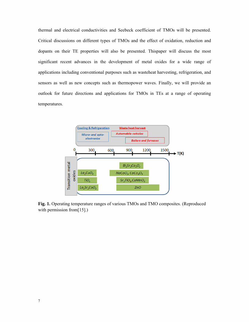
range of interesting thermal properties at cryogenic, ambient and high temperatures (Fig. 1).
Many TMOs offer high Seebeck coefficients, with desired thermal and electrical
conductivities and heat capacities, at targeted temperatures that can be exploited for different
applications[11-14]. Their abundance in nature is another important advantage for
technologies to be widely adopted.
Despite all the aforementioned promising properties, TMOs have yet to achieve their true
potential in the TE realm.This review article will provide a comprehensive outlook on the
TEproperties of various TMOs and assess their performance. Thecritical parameters of
thermal conductivity, electrical conductivity and Seebeck coefficient will be
thoroughlydiscussed. The effect of changing the morphology and nanostructuring on the
7
thermal and electrical conductivities and Seebeck coefficient of TMOs will be presented.
Critical discussions on different types of TMOs and the effect of oxidation, reduction and
dopants on their TE properties will also be presented. Thispaper will discuss the most
significant recent advances in the development of metal oxides for a wide range of
applications including conventional purposes such as wasteheat harvesting, refrigeration, and
sensors as well as new concepts such as thermopower waves. Finally, we will provide an
outlook for future directions and applications for TMOs in TEs at a range of operating
temperatures.
Fig. 1. Operating temperature ranges of various TMOs and TMO composites. (Reproduced with permission from[15].)

8
2 Basic principles of thermoelectricity in TMOs
The fundamental factors that govern TE properties are thermal conductivity (κ),electrical
conductivity (σ) and Seebeck coefficient (S). The performance of TE materialsis generally
assessed by the figures of merit (ZT) defined as S2σ/κ, and the thermoelectric power factor
(TPF) defined asS2σ. In this section, we present an overview of the main equations governing
the aforementioned TE parameters for bulk three dimensional (3D)and low dimensional (2D,
1D and 0D) structures.
2.1 Thermal conductivityκ
Thermal conductivity is the ability of a material to conduct heat. The main contributors to the
thermal conductivity are phonons and charge carriers (electrons and holes). The overall
thermal conductivity(κtotal)of a material is defined as:[16, 17]
= ℎ + (1)
where, κphononis the lattice thermal conductivity due to acoustic phonons travelling through
the crystal lattice and κelectron is the electronic thermal conductivity due to charge
carriers.Phonons and charge carriers can undergo scattering due to other phonons, lattice
defects, impurities, electrons, grain boundaries and interfaces[18]. Such scattering then
results in changes of thermal conductivity.The fundamentals of κphononand κelectronfor bulk as
well as low dimensional materials are discussed next.
2.1.1 Bulk (3D) materials
For semiconducting and insulating TMOs,acoustic phonons are the major contributorsto κtotal.
However, for highly doped and non-stoichiometric TMOs the electronic thermal conductivity
also plays an important role. For bulk materials, the kinetic theory of gases defines the
κphononand κelectron as:

9
ℎ = 13 ℎ (2a)
= 13 = (2b)
where υs is the velocity of sound, Cvis the heat capacity at constant volume, Lph is the phonon
mean free path, cv is the electronic specific heat per volume, v is the electron velocity that can
be assumed to be the Fermi velocity vF, Λ is the electron mean free path, L is the Lorenz
number (2.45×10⁻⁸ V2.K2), σ is the electrical conductivity, and T is the temperature in Kelvin.
Cv and υs are typically temperature independent forT> 300K; hence at high temperatures,
κphonon primarily depends on Lphand can be largely attributed to phonon-phonon
scattering[19].
On the other hand,κelectron depends on the electron mean free path.The Wiedemann-Franz law
as shown in Eq. 2b states that κelectron is directly proportional to σandT, so that any variation in
κelectron affectsσ. Hence,the only TE parameter that is independent of the electronic band
structureisκphonon.
In semiconducting and insulating TMOs, phonons are the majority contributors to κtotal,
making it possible to tune theirκtotalwith a negligible effect onσ. A comprehensive theoretical
analysis of κ has been provided elsewhere[17].In order to improve the performance of TE
materials for conventional applications such as cooling and energy scavenging, a reduction in
κphonon is desirable.In theory, the minimum κphonon is achieved when the mean free path of the
phonons is no more than the interatomic spacing of the constituent atoms[4].Limiting Lph by
confining phonons can help achieve this goal. Such a confinement can be obtained by
creating low dimensional materials, which are described next.

10
2.1.2 2Dmaterials
A two-dimensional (2D) quantum well structure consists of a very thin layer of material that
is nanometers thick in one dimension and semi-infinitely large in the other two dimensions.
2D quantum well structures arelikely to reduce theκtotalof TMOscompared to their bulk
counterparts because phonons mainlyscatter at the interfaces, while the motion of the
electrons can be confined parallel to the layers. κelectron2Dis a strong function of the thickness
of layers (W). For 2D quantum well structures,κphonon2D and κelectron2D along the x-axis (Fig.
2a) have been defined as:[20, 21]
ℎ 2 = 24
( − 1)20
2 = 22
2 /2 3 2 − 20
(3a)
(3b)
where, kB is the Boltzmann constant, h is the Planck constant, e is the electron charge, mx,y,z
are the three components of the effective mass, θ is the Debye temperature, ξ=hω/ kBT (hω
being the phonon energy), T is the absolute temperature, τ is the electron relaxation time and
is defined as τ=μxmx/e where μx is the mobility along the x-axis (Fig. 2a), v is the velocity of
sound, Fiare the Fermi-Dirac functionsand τc is the combined phonon relaxation time due to
all resistive processes (which include boundary scattering, mass difference scattering,
scattering at dislocations and Umklapp scattering processes),which is governed by the
Matthiessen’s rule (see ref.[21]for details). According to Eq. 3a, the theoretical value of
κphonon2D is strongly influenced by the phonon-phonon energy, its relaxation time τc, which is
a function of the quantum well dimension and temperature.
κelectron2D depends only on two effective mass components of the electrons as shown in Eq.3b.
This is because, unlike phonons,electrons can only move in a 2D motion parallel to the layers

11
due to the quantum confinement.Additionally, a stronger confinement (by decreasingW) is
expected to increase κelectron2D.However, the result of reducing W is generally a decrease in
the overall thermal conductivity. This is especially useful in engineering ZT when both
Seebeck coefficient and electrical conductivity of the material remain constant. There are
practical examples of employing 2D TMOs such as TiO2, cobalt oxides and manganese
oxides[22] which will be discussed in their relevant sections. The application of 2D TMOs
with increased ZT values[22]has been demonstrated in energy scavenging at elevated
temperatures that will also be discussed later.
2.1.3 1D materials
Hicks et al. developed a theoretical model and predicted that materials in 1D form (such as
quantum wires, nanobelts and nanorods) can result in further reduction of κelectron, compared
to bulk and 2D structures[23]. The thermal conductivity of phononsin 1D structureswere
theoretically modelled by Zou and Balandin.[24] The equations describing κphononand κelectron
for 1D structures are:[23, 24]
ℎ = 24
( − 1)20 × 1 − ( ( ), )
= 2 2/2 ( ) /2 2 5 /2 − 9 /22
/2
(4a)
(4b)
where, a is the width of a 1D structure with a square cross section, mx is the effective mass
component in the x direction (Fig. 2b), v is the phonon group velocity, T is the temperature, θ
is the Debye temperature, ξ=hω/ kBT (hω being the phonon energy), Λ is the phonon mean
free path (Λ(ξ)=v(ξ)τc(ξ)), η is the ratio between the wire width and Λ (η(ξ)=a/Λ(ξ)), p is a
parameter which characterizes the interface roughness and its effect on the phonon scattering.
12
The value of p represents the probability of a phonon undergoing diffusive scattering (refer to
[24] for additional details). Other parameters have been defined in Eq. 3a & 3b.
The theoretical ZT calculations using Eqs.4a and 4b for a 1D structure show that it strongly
depends on its width. For widths smaller than the thermal de Broglie wavelength ofthe
carriers, the ZT increases significantly with decreasing the width of the 1D structure.TMOs
such as ZnO and TiO2 havebeenextensively synthesised in 1D morphologies (nanorods,
nanoribons and nanotubes)[25, 26]and the thermal conductivity of such materials are strongly
affected by such morphological manipulations[25].
2.1.4 0D materials
Unlike 2D or 1D structures, the carriers in 0D structures such as quantum dots are confined in
all directions. The transport mechanism in 0D structures is thus different from others, in the
sense that unconventional conduction behaviour such as tunnelling is required to maintain its
electronic conductivity. Therefore, 0D structures such as quantum dot superlattices (QDSLs)
and segmented nanowires (SNWs) were proposed to provide a conduction pathway. As the
name suggests, such segmented structures consist of a series of interwoven quantum dotsof
two different materials(Fig.2c). The electronic transport along the wire axis occurs by
tunnelling between adjacent quantum dots. Furthermore, due to the wire boundaries and
interfaces between the quantum dots, the phonon conduction along the wire axis is impeded,
resulting in a reduced lattice thermal conductivity.
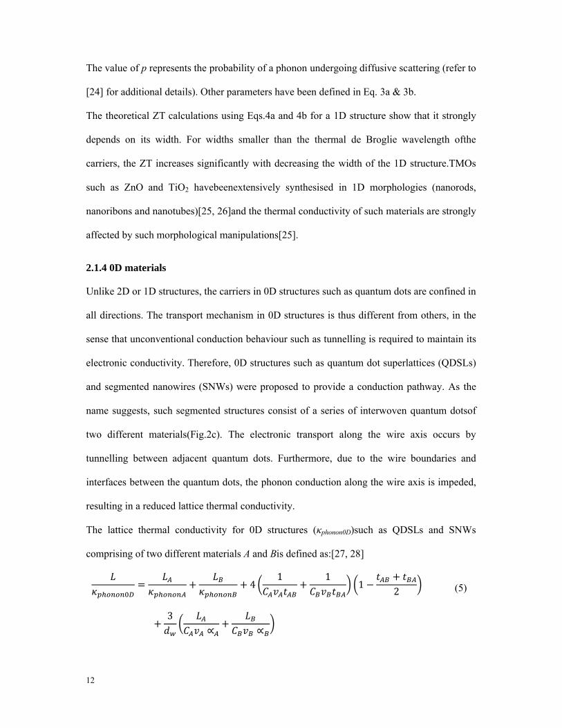
The lattice thermal conductivity for 0D structures (κphonon0D)such as QDSLs and SNWs
comprising of two different materials A and Bis defined as:[27, 28]
ℎ 0 = ℎ + ℎ + 1 + 1 1 − +
+ 3 ∝ + ∝
(5)

13
where, CA,B is the heat capacity, vA,B is the sound velocity of the nanodot material, LA,Bis the
length of the material’s segment, tABand tBAare the average transmissivity of phonons from
quantum dot A to B and vice versa, αA,B is the geometric factor that depends on the aspect
ratio (LA/dw or LB/dw) of the quantum dots in which dwis the diameter of the wire. The first
twoterms in Eq.5 account for the intrinsic phonon scattering events, while the third and fourth
terms account for the contribution of the segment interface and the wire boundary scattering
processes to the κphonon0D. It is evident that the segment length, the choice of materials A and
B, as well as the aspect ratio of the quantum dots play a vital role in determining κphonon0D and
hence, the design of the QDSL or SNW structure is the most important factor governing the
thermal properties. In order to quantify the electronic contribution of the thermal conductivity
(κelectron0D) in a QDSL or SNW structure, the Kroenig-Penney model is used. This model
determines the dispersion relation En,m(k) for the electrons that move along the axis in the n,m
sub-band of the wire experiencing a square periodic potential[29], wherek is a 1D wave
vector that describes the energies of these electrons in the square potential[28].The electronic
band structure of each sub-band is highly dependent on the segment length (LA or LB), the
potential barrier height and the transport effective masses[28].
The constant relaxation time approximation is used for calculating the following fundamental
integrals for the conduction band:[27]
( ) = 2 2 21, ( ) ( ,
,− ) − (6a)
, ( ) = ,(6b)
where, α=0,1 or 2, τ is the relaxation time of the carriers, EF is the Fermi energy, f(E) is the
Fermi-dirac distribution function and gn,m(E) is the density of states of the n,msub-band,which

14
is defined in Eq. 6b. The electronic component of thelattice thermal conductivity in 0D
structures (κelectron0D) is defined as:[27]
0 = 1 (2) − ( )2(0)
/2(7)
From Eq. 6a, b & 7, it is clear that κelectron0Dis strongly dependent on the diameter of the
SNWs, as well as the carrier relaxation time. However, as discussed before, the electronic
contribution towards the thermal conductivity in semiconducting TMOs is generallymuch
lower, compared to the phonon contribution at small diameters.The superlattice interfaces in
TMO-based 0D structures such as SNWs are expected to enhance the phonon scattering to
further suppress the thermal conductivity compared to the bulk form[30].
The above discussion shows that a reduction in the dimensionality of the system can result in
a reduced lattice thermal conductivity, due to the phonon mean free paths being limited by
the nanostructuring,and consequently increased phonon scattering. This can potentially
enhance the efficiency of TE TMOs for energy scavenging applications, while can increase
the performance of temperature sensors, which are based on such structures.
2.2 Electrical conductivityσ
The electrical conductivity of TMOs in bulk and low dimensional form has been extensively
studied[31-34]. Most TMOs exhibit low σ in their bulkdue to low mobilities of charge
carriers[35]. However, it has been shown that quantum confinement of these carriers alters
the electronic density of states (DOS). Various nanostructuring and doping techniques can be
employed to alter the carrier concentrations by adjusting the bandgap and surface energy in
TMOs[31].In this section, we will discuss the theoretical equations that govern the electrical
conductivity of TMOs in bulk and low dimensional forms.

15
2.2.1 Bulk (3D) materials
Forbulk TMOs, the electrical conductivity can be defined in a simplistic form as follows:[16,
29]
= ( ) ( ) = ( ) 2 ( )∗
(8)
where, n(E) is the density of carrierswhich is a function of the density of states g(E), e is the
electronic charge, μ(E) is the differential carrier mobility, τ(E) is the relaxation time and m* is
the carrier effective mass.
The m* of manyTE TMOs such as TiO2 and layered cobalt oxides isrelativelylarge.[16,
36]Additionally, they also suffer due to short relaxation times[37-39]. As a result, the charge
carrier mobilities of many TMOs are relatively small. The carrier concentrations of bulk
TMOs, which is affected by the thermionic effect, depend on their bandgap and temperature.
As a result, the carrier mobilities and concentrations in TMOs can be tuned using various
doping and nanostructuring techniques.
2.2.2 2D materials
The electrical conductivity of TMOs can be enhanced by fabricating quantum well structures,
which result in the quantum confinement of carriers. For a 2D quantum well structure
discussed previously in section 2.1.2, Hicks et al. defined the electrical conductivity (σ2D)
as:[20]
2 = 1 ∗ ∗ /2 0 2 (9)
where, W is the quantum well width, ∗and ∗ are the effective mass components in the x
and y direction (in the plane of the 2D material) respectively, F0 is the Fermi energy, e is the
electron charge, μx is the mobility, T is the temperature, kB is the Boltzmann constant and h is

16
the Planck’s constant.In such structures the electrons are confined only to a 2D motion that is
parallel to the layers. Eq.9 shows that a reduction in Wenhances σ2D. In TMOs, the Fermi
level can be adjusted using various doping techniques and methods that control
stoichiometry.In these materials, the Fermi level is a strong function of morphology and the
temperature[40].As expected, enhanced electrical conductivities have been demonstrated in
various 2D TMOs such as MoO3, CoO2 and ZnO nanobelts[41][42][43].
2.2.3 1D materials
In morphologies such as one-dimensional nanorods, nanotubes or nanobelts of TMOs,σ is
predicted to increase by reducing the cross sectional area of the structure. Such enhancement
is mainly due to increased charge carrier mobilities via changes in DOS[44, 45].σ in such 1D
structures is defined as:[23]
= 12 ( ∗) /2 /2 2
/2(10)
where, a is the width of a1D structurewith a square cross section, ∗ is the effective mass
component in the x direction. Other parameters have beendefined in Eq. 9.Additionally, σcan
be tuned by changing the Fermi level of the TMOs, which result in the carrier concentration
change as well[46][47].
TMOs such as TiO2and ZnO are widely synthesised in various 1D morphologies[25, 26]. As
predicted, σ in such quasi-1D structuresis shown to increase compared to the bulk forms[46].
The carrier concentrationsin such structures can be adjusted by the use of suitable dopants[46,
48].There are many good review articles that coverthe topic of electrical conductivity in
various 1D TE TMO structures[46, 49].

17
2.2.4 0D materials
QDSL or SNW structures, described in section 2.1.4,allow for electrical conduction through
mechanisms such as tunnelling or hopping. Well-separated discrete energy states of the
segments alter the fundamental properties such as DOS and bandgap energy in an alternating
manner along the 1D wire[50, 51].At the same time, the 0D characteristics, and in particular
the electrical conductivity, of each quantum dot is maintained by the energy differential of
the conduction or valence bands between the two constituent materials that form the
wire[28].The electrical conductivity for such 0D structures is defined as:[27, 28]
0 = 2 (0) (11)
K(α) is defined in Eq. 6a. It can be seen from Eq.11 that the σ0D is a strong function of the
diameter as well as the electronic DOS.An enhanced σ is expected in QDSL and SNW
structures with reducing diameters. This is mainly because of the increased carrier relaxation
times in such low dimensional structures[51].
2.3 Seebeck coefficientS
The Seebeck coefficient is the magnitude of the induced voltage divided bythe temperature
gradient across a material. The Seebeck effect is caused by charge-carrier diffusion and
phonon drag. Many TE TMOs such as TiO2, ZnO, CoO and MnO2exhibit large Seebeck
coefficients.High Svalues in TMOs usually arises from either high effective masses (m*)due
to electronic correlations[52]or from electron–electron interactions[53]. An enhancement in
the Sof TMOs can be achieved by altering the DOS through nanostructuring techniques. The
theory governing the S of bulk and low dimensional TE TMOs is presented in this section.
2.3.1 Bulk (3D) materials
For semiconducting TMOs in bulk form, the simplified Seebeck coefficient can be estimated
by the following expression:[16]

18
= 8 ∗ 2 23 2 3
2/(12)
where, n is the carrier concentration, m* is the carrier effective mass, e is the electronic
charge, T is the temperature, h is Planck’s constant and kB is the Boltzmann constant.
Eq.12 shows that a higherm*results in larger Seebeck coefficients. TMOs usually exhibit high
effective carrier masses, which explain the high S values observed in many TMOs. From Eq.
12 it is also predicted that in an increase in Talso enhancesS. Dramatically enhanced S has
been observed in many TMOs such as ZnO and MnO2 at elevated temperatures[5, 9]and will
be discussed in their relevant sections.
2.3.2 2D materials
2D quantum well structures can result in enhanced S of TE TMOs materials due to changes in
the Fermi energy of the carriers as well as the electronic DOS. For a 2D quantum well
structure,the Seebeck coefficient is defined as:[20]
2 = − 0 − 2∗
2∗ = 1 − 2 2 21 − 2 2
∗ 2
(13a)
(13b)
where, kB is the Boltzmann constant, e is the electron charge, EF is the Fermi energy, T is the
temperature, ∗ is the component of the effective mass, W is the quantum well width and Fi
are Fermi-Dirac functions. χ*2D is the reduced chemical potential for quasi-2D structures.
The decrease in W of the quantum well is predicted to result in an enhanced S as can be seen
from Eq. 13a &b. Additionally, the electron filtering (i.e. only high energy electrons can pass
while others are scattered)[54] in such low-dimensional heterostructures is expected to
decouple the S and σ, allowing fairly independent control over these properties. The

19
phenomenon of electron filtering is explained in more detail elsewhere[51, 55]. In 2D TMOs,
anincrease inShas been experimentally observed. Ohta et al. demonstrated dramatic
increasesinS(up to ~ 5 times) for 2D electron gas (2DEG) systems based ondoped TiO2 which
will be discussed in detail in Section 4.1.3[56, 57]. 2D layered cobalt oxides and rhodium
oxide also show higher S compared to their bulk forms[58, 59].
2.3.3 1D materials
TMOs are widely synthesised in various 1D morphologies[26, 60-62].Size reduction to a
single dimension is expected to enhance Sdue to the altered DOS. The S for a 1D structureis
defined as:[23]
= − 3 /2/2 −
(14)
where, Fi is the Fermi Dirac function, e is the electronic charge, kB is the Boltzmann constant
and η=ζ/kBT is the reduced chemical potential, in which ζ is the chemical potential relative to
the lowest bound state. In a 1D structure, Sis influenced by the Fermi level of the carriers
(Eq.14), which in turn is strongly influenced by the width of the 1D structure.(see ref.[23] for
details). Hence, an enhancement of Sis predictedwith decreasing width of the 1D structure.
Sis also a function of the energy derivative of the electronic DOS[35]. As the dimensionality
decreases, an increase in Seebeck coefficient is expected becauseofchanges in the DOS due to
quantum confinement[20, 21, 23, 63]. Due to theextensive information that is available about
the crystal structures of TMOs, such morphological tuning of the DOS can be conveniently
carried out. As predicted, the Sin 1D TE TMO such as ZnOnanowiresis shown to increase
due to quantum confinement[49] and exhibits a value of ~ –450 μV/K at room temperature.

20
2.3.4 0D materials
QDSL and SNW structures as described in section 2.1.4exhibit sharper DOS compared to
higher dimensional structures, due to the superlattice-like structure along the wire axis
(Fig. 2c). An electronic structure with sharp maxima in the DOS like this is predicted to be
the best for TE materials[50, 64].Due to their unique electronic band structure and sharp
density of states, an enhancement of S is expected in QDSLs and SNWs[50].
The Seebeck coefficient of a segmented nanowire is defined as:[27, 28]
0 = − 1 ( )(0) (15)
From Eq.6 a, b and 15it is obvious that a sharp maximumin the electronic DOS(Fig. 2d)will
result in a strong increase in the Seebeck coefficient.As the diameter is decreased, the size
quantisation effects prevail, resulting in an enhanced S. The increaseof Sin such 0D TMO
structures is expected to be more pronounced. Even though metal oxide based SNWs have
been synthesised[46, 65],there are no reports investigating their Seebeck coefficients. This
presents a vast potential for future work in the field of TE TMOs.
From the discussion in this section,it is evidentthat reducing the dimensionality of TMOs
offers opportunities to tunethe key TE parameters of κ, σ and S independently. There has been
a continuous development in thesynthesis techniques of TMOsand there is a vast amount of
information available about their crystal structure, phases and various morphologies. This
allows flexibility in their fabrication which can be carried out at both large and small scales
using liquid and gas phase deposition techniques, allowing tuning of their TE properties at
low dimensions to engineer TMOs with high TPFs and figures of merit. A recent review
article comprehensively discusses the latest developments in the synthesis of metal oxide
nanostructures[66].

21
Fig. 2.(a) A 2D quantum well structure with width square cross section of width a, (c)comprising of quantum dots (0D) of lengths LA and LB. (d) Energy dependence of the materials. ((c), (d) Reproduced with permission from
3 Strategies to tune and alter TE parameters of
The TE performance of TMOs is assessed on the basis of the application.
TMOs can be classified into four majorcategories: (1)c
scavenging from heat, (3) sensors and (4) t
discussed in detail insection 5.For cooling,
along with a lowκ is desirable[67
be either high or low depending
high TPF and benefit from a high
TMOs depends on the application.
Furthermore, a fundamental understanding of the carrier transport processes contributing to
the TE effect in TMOs is required. There are however, many complexities in determining the
A 2D quantum well structure with width W, (b) 1D conductor (nanowire)(c) a segmented nanowire superlattice of diameter
comprising of quantum dots (0D) of alternating materials A and B, with respective segment (d) Energy dependence of the electronic DOS in 3D, 2D, 1D and 0D
materials. ((c), (d) Reproduced with permission from [28] and [29].)
tune and alter TE parameters of TMOs
TMOs is assessed on the basis of the application. Applications
four majorcategories: (1)cooling and refrigeration,
) sensors and (4) thermopower wave sources, all of which will be
For cooling, refrigeration, and energy scavenging, a high TPF
67, 68]. Sensors generally require high Sand lowκ
ing on the type of sensor.Thermopower wave sources require
benefit from a highκ[5-7, 69]. Hence, the tuning of the key TE parameters in
TMOs depends on the application.
fundamental understanding of the carrier transport processes contributing to
the TE effect in TMOs is required. There are however, many complexities in determining the
(nanowire) with a a segmented nanowire superlattice of diameter dw
materials A and B, with respective segment and 0D
pplications of TE
ooling and refrigeration, (2) energy
which will be
energy scavenging, a high TPF
κ, while can
wave sources require a
the key TE parameters in
fundamental understanding of the carrier transport processes contributing to
the TE effect in TMOs is required. There are however, many complexities in determining the

22
key quantities in electron and phonon transport both theoretically and experimentally[70-
72].Tuning of transport properties of TE TMOs, such as reducing electronic thermal
conductivity[73] or reducing the bipolar effect[74, 75], is possible. In their recent review
papers, Minnich et al.[72] and Zebarjadi et al.[70] have extensively covered the challenges
and strategies for improving our understanding of carrier transport processes.
In this section, the techniques that are commonly used to alter the TE parameters of TMOs
are briefly discussed.
3.1 Optimization using stoichiometry and doping techniques
The incorporation of dopants and altering of stoichiometry are widely employed for
adjustingthe TE parameters of TMOs[76]. The type of application plays a crucial role in
determining the correct technique in this regard[77]. For cooling, refrigeration, heat
scavenging and sensing applications, methods that reduceκphonon are generally desirable.
Crystal disorder in the unit cell can be created by dopingor altering stoichiometry ofthe TMO
crystal lattice[34]. Such manipulations change the vibrational properties of the crystal and
influence κphonon[16] or by introducing additional scattering sites for phonons, thereby
limiting κphonon[78-82].κelectron is also affected by changing the stoichiometry and doping level
of the TE TMOs. κelectron depends on the electrical conductivity of TMOs (Eq. 2b) and is also
a function of the Fermi level and charge carrier concentration, which are directly affected by
changes of stoichiometry or incorporation of dopants[17].In many refrigerationand heat
scavenging applications, high electrical conductivity is desired,which generally directly
increases κelectron. However, this is not desirable as it enhances the exchange of heat between
two sides. Hence, doping, compositing and processes altering the oxygen deficiency can be
implemented to achieve the desired thermal conductivity. Conversely, in thermopower wave
sources, high TPF and κ are desirable. This can be achieved by the use of metallic dopants or
reducing the TMOs to a degree that the Seebeck coefficient is not compromised. Such

23
dopants result in enhanced TPFs in TMOs such asZnO and CoO2, which will be discussed in
details in sections 4.4 and 4.7 respectively[83-95][96].
After incorporating dopants and altering the stoichiometry, the most challenging issue is the
determination of electronic band structures[70]. Theoretical methodssuch as density
functional theory (DFT) can help;however, underestimation of the band gap by DFT
calculations generally results in inaccuracy of theoretical predictions of the Seebeck
coefficient and the bipolar effect[70]. Many methods have been developed to address this
issue, such as the dynamical mean-field theory (DMFT)[97] which has been successfully
applied to the case of TMOs[98].
The calculation of electron mobility and carrier lifetime is even more challenging. First
principles calculations can only be performed on limited supercell sizes and the inclusion of
long range potentials is difficult[70]. More importantly, inelastic scattering mechanisms at
the elevated operating temperatures of TE TMOs renders relaxation time approximations
(RTA) calculated from first-principles and DFT mostly invalid[99, 100]. The details of
carrier lifetime in many TE TMOs are still relatively unknown. Hence, an improved
fundamental understanding of the mechanisms governing the formation, stability, and
properties of interfaces is required[54].
3.2 Substructuring
In engineering TE TMOs, it is generally desirable to decouple κphonon andκelectron. For many
refrigeration and heat scavenging applications it is desired to adjust κphononwithout
affectingσ(hence κelectron). Substructuring (or segmentation) approaches are suggested to be
efficient for such manipulations. Substructuringrelies on a periodic arrangement of layers
withdifferent electron and phonon transport characteristics, resulting in a complex material
structure with distinct regions providing particular functionalities (Fig. 3). For many

24
refrigeration and heatscavenging applications, an ideal TE TMO would comprise a high
mobility semiconductor region entwined with a phonon scattering region that houses
disordered structures (dopants and lack of stoichiometry), without affecting the carrier
mobilities of the other region[16]. A detailed discussion on the substructuring approach is
provided in another review[16]. TMOs occurring as natural superlattices can provide an
independent control of transport properties, providing an excellent platform to engineer high
performance TE materials. TMOs such as the doped cobalt oxide systems are a classic
example of the benefits of substructuring approach, which will be discussed in detail
later[11]. Another advantage of TMOs is that theycan be fabricated in a variety of well-
studied structures and a large number of synthesis techniques to fabricate them in different
morphologies and structures have been well-established, making the substructuring approach
highly attractive in order to tune their TE parameters according to the desired application.
Fig. 3. Schematic depiction of the substructuring approach in doped cobalt oxide, comprising of ordered CoO2 layers that are separated by disordered layers (of Na dopant) to achieve a good electrical conductivity and poor phonon conductivity. (Reproduced with permission from[42].)

25
3.3 Nanostructuring
As discussed earlier, the S, σ and κ for conventional 3D crystalline TMOsare interrelated and
cannot be controlled independently. Any increase in σ results in an enhancedκelectron(Eq. 2b).
Additionally, a change in the Fermi level and carrier concentration affects both κelectron and
κphonon.
Atthe nanometer scale, there are significant changes to the electronics of TE TMOs(see
section 2), which allow for alternative techniques to control the S, σ and κ in a relatively
independent manner. In nanostructured materials, quantum confinement effects [51] and
surface properties become much more important, and result in properties that are changed
from those of the bulk forms.The quantum confinement of carriers in nanostructured TMOs is
predicted to enhance both their TPF and ZT (see section 2.2 and 2.3)[63]. Additionally, it is
well known that nanostructuring of TMOs alters their Fermi level and carrier
concentration.[31]Nanostructures also introduce additional scattering mechanisms. If the
spacing between the nanoparticles is larger than the electron mean free path (MFP), they will
act as an additional source of electron scattering in the host material. If however, the spacing
is smaller than the electron MFP, the scattering mechanisms will become much more
complex since the leakage of the electron wave into the nanoparticles is no longer
negligible.[70, 101]The nanostructuring technique has resulted in enhanced TPFs and ZTs in
TMOs such as TiO2, ZnO, cobalates and manganates which will be discussed in detail in
Section 4[56][91][102, 103].
In addition to the electronics of TMOs, their phonon propagation properties and as a
resultκphonon can be tunedviananostructuring (see section 2.1), resulting in enhanced phonon
scattering andaltered phonon mean free paths.[103]If the dimensions of semiconducting TE
TMOsare smaller than the mean free path of the phonons, but larger than the mean free path
of the charge carriers, a reduction in κphononcan be obtained due to boundary

26
scatterings,without affecting σ. Koumoto et al. have reviewed the progress in the
development of nanostructured TE TMOs[22].
Nanostructuring can be implemented to decrease the lattice thermal conductivity by
introducing many interfaces with spacing smaller than the phonon mean free path. Although
reducing lattice thermal conductivity through alloying and/or nanostructuring techniques has
been the most effective way to improve performance of TE TMOs for conventional
applications, details of phonon transport mechanisms are still not very well understood[72].
Even in bulk form, theoretical and experimental determination of quantities such as phonon
mean free path is still a challenge[72]. Phonon transport models based on Callaway model of
thermal conductivity[104] usually require adjusting various fitting parameters causing
inconsistency in the models fundamental predictions such as phonon’s wavelength and mean
free path. Calculations of the thermal conductivity and phonon mean free path in TE TMOs
using combined density functional theory (DFT) [105, 106] and molecular dynamics
(MD)[107-109] simulations on the other hand are difficult and computationally costly
because of the extremely complex crystal structure of alloys and misfit layered oxides.
Moreover, the introduction of many interfaces in the material via nanostructuring adds more
complexity to the problem.
The problem is even more complex in case of electron transport. In case of heavily doped
complex TE TMOs, the standard analysis based on the Boltzmann equation with the
assumption that the mean free path is much larger than the de Broglie wavelength leads to
inaccurate results[72, 110].Nanostructuring further complicates the problem as the interfaces
introduce complex scattering mechanisms that should be accounted for in theoretical
analysis[111]. Therefore, modeling the transport phenomena in bulk and nanostructured TE
TMOs would require more powerful tools such as the non-equilibrium Green’s functions with
the inclusion of electron wave effects[72].

27
3.4 Compositing
It is suggested that composites can be useful in controlling TE parameters of TMOs,as they
can be designed to show high density of the interfaces[112], that can be used for adjusting
both phonon and electron scattering. TMO composites’distinct advantagesare their cost
effectiveness and scalability[113]. An excellent review article discussing the impact of the
bulk composite engineering approacheson S, σ and κcan be seen in ref. [72]. Composites of
TMOs have resulted in enhanced TPFs, which will be discussed later in the relevant
sections[91, 114].
4 Transition metal oxides and their TE properties
In this section, the most common TMOs that have been investigated for their TE properties
will be discussed. An overview of their crystal structures and their TE properties in doped
and various stoichiometry conditions will be presented. Additionally, different synthesis
methods of these TE TMOs will be illustrated. For further information regarding the
structures, properties and syntheses of TMOs, the readers can refer to comprehensive text
books in this field[115-117].
4.1 Titanium oxides – TiOx
4.1.1 Crystal structure
TiO2 is one of the most investigated metal oxides for a wide variety of photocatalytic, TE,
solar cell, biosensing and gas sensing applications.TiO2 has a bandgap of ~3.2 eV in its
intrinsic form[118]. The most common polymorphs of TiO2 are anatase, rutile and brookite.
Rutile and anatase exhibit a tetragonal structure, while brookite is orthorhombic[119]. The
transformation with increasing temperature usually follows the sequence: anatase→
brookite→ rutile. Generally in between room temperature and 598 K anatase is the dominant
polymorph. Above 625 K, the anatase transforms to brookite[120]. Heating of titania in the

28
temperature range of 873 to 1275 K leads to an alteration of phase stabilities, and it
transforms almost completely to rutile. Many reviews on the various crystal structures, size
and temperature dependence of the different polymorphs as well as different morphologies of
stoichiometric and non-stoichiometric TiOx exists[119-121].
4.1.2 TE properties of stoichiometric TiO2
TiO2 can be synthesised in many different morphologies such as spheroidal nanocrystallites,
nanoparticles, nanotubes, nanosheets, nanofibers and epitaxial thin films[122]. The room
temperature S of crystalline TiO2 is reported to be approximately −600 μV/K, while σ of the
order of 103 S/m is observed, resulting in a TPF of 360 μW/m.K2. The κ at room temperature
is ~ 5.8 W/m.K and is reduced with increasing temperature (~ 2.8 W/m.K at
1073 K)[123].Owing to a moderate σ and high κ, the ZT in pure TiO2 is low (< 0.025)[123,
124]. However, non-stoichiometric TiO(2-x) has been demonstrated to be promising for TE
applications at both cryogenic [125] and elevated temperatures[124]. The TE properties of
reduced, oxidized and doped TiO2 are discussed next.
4.1.3 TE properties of non-stoichiometric, doped and composite TiOx
Non-stoichiometric TiOx can show fascinating TE properties both at elevated and cryogenic
temperatures. Tsuyomoto et al.have shown that TiOx (x=1.94) with an orthorhombic crystal
structure, exhibits a peak S of – 518 μV/K and σ of 2×10³ S/m at ~350 K. They demonstrated
that both S and σ increase with temperature, resulting in a TPF of ~540 μW/m.K2 at
343 K[126]. Interestingly, single crystal rutile TiO2 reduced to TiO(2-x)via annealing in H2 at
elevated temperatures as high as 1050 K shows exceptionally high TPFs at cryogenic
temperatures. TiO(2-x) generates enlarged phonon scattering by the defect planes, resulting in
low thermal conductivities (0.83 W/m.K). Fig. 4a &4b depict that TiO(2-x) can exhibit an
extraordinary S of up to –60,000 μV/K, with TPF and ZT of ~ 1.7×10⁴ μW/m.K2 and 0.1,
respectively, at temperatures in the range of 10 K[125]. Another study showed that non-

29
stoichiometric TiO(2-x) with a rutile crystalline structure, formed after annealing and reduction
in a carbon environment at 1373 K, demonstrates a TPF of 100 μW/m.K2 at temperatures of
up to 550 K[124]. Obviously, the introduction of oxygen vacancies in the TiO2 crystal result
in enhanced σ due to an increase in carrier concentration (Eq. 8). In contrast, a prolonged
oxidation of TiO2 at elevated temperatures, results in lower σ and S (– 600 to +150 μV/K) and
therefore low TPFs and ZTs (<0.1). Additionally, a transition from n-type to p-type is also
observed in the oxidation process, at temperatures around 1300 K[127].
In addition to the change of stoichiometry, the doping technique is usually employed to tune
the TE properties in TiO2. As discussed in section 3.1, metallic dopants are useful as they
result in enhanced electrical conductivities. Additionally, the doping process creates crystal
disorder, which reduces the lattice thermal conductivities. It has been shown that Na doped
titanate nanotubes (DTNTs) with a composition such as Na2-xHxTi3O7 result in TPFs ranging
between 174 - 280 μW/m.K2, and a peak ZT of 0.3, at elevated temperatures (745-1032
K).[128] 2% Nb doped, anatase, n-type TiO2 epitaxial films show a TPF and ZT of
250 μW/m.K2and 0.25, respectively, at 900 K[129]. Similar observations have also been
made by Sheppard et al. at elevated temperatures[130, 131].
Fig. 4. (a) Seebeck coefficient (red) and electrical resistivity (blue) of reduced single crystal rutile TiOx as a function of annealing temperature and (b) Seebeck coefficient as a function of temperature for a sample annealed in H2 at 1053 K. (Reproduced with permission from [125].)

30
A TiO2composite commonly investigated for its excellent TE properties is strontium titanate
(SrTiO3), also known as STO[1, 57, 132]. STO is a perovskite type oxide that exists in an
isotropic cubic crystal structure at temperatures above 100 K. Additionally, it shows a strong
structural tolerance to substitutional doping. Due to its d-band nature, the effective mass of
carriers is quite large in STO, resulting in a high S(Eq.12). Additionally, STO exhibits a very
high melting point (~2350 K), suggesting its stability at high temperatures[22].
In itspure form, STO is essentially an insulator; however, it can be tuned to be
semiconducting or metallic by substitutional doping with La3+ or Nb5+[57]. The highest TPF
and ZT for La and Nb doped STO single crystal has been reported to be 3600 μW/m.K2 and
0.1, respectively at room temperature, while the corresponding values at 1000 K, are
865 μW/m.K2 and 0.27, respectively (Fig. 5a-e)[133][1, 132][134]. A number of studies on
the TE properties of La and Nb doped STO thin films exist[129][134][135]. The ZT values
are limited primarily due to its high κ (∼11.0-3.2 W/m.K in the temperatures of 300-1000 K
respectively)[22]. This high κ value can be ascribed to the perovskite type structure of STO,
which even in the presence of dopant cations as point defects, lacks effective phonon
scattering centers.
Muta et al. suggested that a Ca2+ substitution at Sr2+ sites may result in reduced κ, as it is
established that such substitutions result in the introduction of defects that usually lower
κ[136]. However, Yamamoto et al.have reported that such an approach results in a dramatic
reduction of the TPF, which indicates that any further improvement in ZT is almost
impossible to achieve in a conventional 3D bulk state of STO[137].
A reduction in the STO dimensionality is a strategy that is predicted to enhance TE properties
by offering independent control of the key TE parameters (section 2). The fabrication of a
two-dimensional electron gas(2DEG) can be useful as it results in a 2D quantum confinement

31
of carriers. Ohta et al. utilized a high density 2DEG, which is confined within a layer of STO
that has a thickness of a unit cell (0.3905 nm)[56]. Such 2DEG is realized in
SrTiO3/SrTi0.8Nb0.2O3 superlattices and TiO2/SrTiO3 heterointerfaces. It was shown that in an
optimised state, a 2DEG exhibits a massive TPF of 1.0 × 10⁵ μW/m.K2. The resultant ZT at
room temperature was approximately 2.4 even if a κ value of a bulk single crystal STO is
used (12 W/m.K). A recently published review article discusses new developments in STO
based thermoelectrics in detail[78].

32
Fig. 5. (a) Electrical conductivity, (b) Seebeck coefficient, (c) thermal conductivity, (d) TPF and (e) ZT vs temperature for different concentrations of La dopant in STO thin films.(Reproduced with permission from [134].)
4.1.4 Methods of synthesis
Many different vapour chemical based methods have been used for forming TE TiO2
materials. Chemical synthesis which involves sol gel hydrolysis, electrochemical methods
such as anodization of Ti and hydrothermal synthesis have been commonly used for

33
producing doped or non-stoichiometric TiO2, as the concentration of dopants and
metal/oxygen ratios can be readily controlled in such methods[122],[138][128].
Vapour deposition techniques including sputtering and pulsed laser deposition (PLD) have
also been commonly used for forming highly crystalline TiO2 with predetermined
concentrationsof dopants[129]. STO thin films doped with both La and oxygen vacancies
have been shown to be synthesized using the PLD technique[134][139]. PLD can also be
used in forming 2DEG STO crystals comprised of superlattices of insulating/ Nb-doped
layers of STO to achieve very high TPF of 1.0 × 10⁵ μW/m.K2[56, 57].
4.2 Manganese oxides –MnOx
4.2.1 Crystal structure
MnO2, the most common form of manganese oxide, is a small bandgap (~ 1.3 eV), n-type
semiconductor and is widely used for electrodes in supercapacitors, electrochemical batteries
and microbial fuel cells[140]and as a catalytic material[141]. It exists in a number of
structural forms[142, 143]. The most common polymorphs are the α-MnO2 (psilomelane -
monoclinic structure) and β-MnO2 (pyrolusite-rutile structure)[140]. Other forms knownas δ-,
γ- and λ-MnO2 also exist, and differ in the way in which the MnO6 octahedra are linked[138,
144, 145]. A detailed study of various crystal phases of MnO2 is presented elsewhere[143].
4.2.2 TE properties of stoichiometric MnO2
β-MnO2 has been reported to be promising for TE applications at elevated temperatures[9,
142].Although, the semiconducting properties of α-, β- and γ-MnO2 have been studied in
detail,[146] their TE properties have not been widely investigated, and only a limited number
of studies exist. It has been reported that bulk and thin film β-MnO2 exhibit S of
approximately –300 μV/K and σ of 103 S/m, resulting in a TPF of 90 μW/m.K2[147].
34
Recently, Song et al. reported extremely high Seebeck coefficients in β-MnO2
nanopowder[142]. The S and σ of the MnO2 thin films have been shown to increase
dramatically with temperature[9].ASeebeck coefficient of approximately –1900 μV/K at a
temperature of 623 K has been demonstrated. The σ of the thin films at such elevated
temperatures is ~103 S/m, resulting in a TPF of 3600 μW/m.K2. The κ for MnO2 is reported to
be approximately 4 W/m.K[9].
Although the TPF of MnO2 is high, its ZT is still low. As suggested in section 3.3,
nanostructuring can be used to tune the TE properties of a material. MnO2 nanostructures
such as nanorods and nanowires have been synthesized via various methods[9, 142].
4.2.3 TE properties of non-stoichiometric, doped and composite MnOx
Doping and compositing are good strategies that can be used for increasing TE performance
of MnOxby introducing defects in the crystal structure, thereby impeding the lattice thermal
conduction. Polycrystalline, bi-layered LaSr2Mn2-xCoxO7 (x<0.2) has been reported to exhibit
extremely low TPFs[148]. However, the most commonly reported manganate stoichiometry
for TE applications is the perovskite type CaMnO3. It exhibits an orthorhombic symmetry in
which each Mn atom is surrounded by six Mn neighbours. It occurs in two anti-ferromagnetic
crystal phases: the A-type and G-type, out of which the G-type phase is more stable. The G-
type phase exhibits an indirect bandgap of 0.7 eV, which accounts for its perfect
semiconducting behaviour[149]. The mixed valent, perovskite electron doped manganite
CaMnO3 has been shown to be a promising n-type TE material, especially at high
temperatures[79]. This perovskite system exhibits S of –350 μV/K and σ of 50 S/m, resulting
in a TPF of 6.1 μW/m.K2, which is very low for TE applications. However, the electrical
conductivity of such an oxide can be enhanced by introducing suitable dopants[22].The
manganate may be doped on either site. The most commonly used dopant is ytterbium (Y) on
the calcium site and niobium (Nb) on the manganese site. The Y doping is particularly

35
beneficial as it results in a lower κ and has been shown to be the most effective dopant[78-
81].
A peak TPF of 300 μW/m.K2 has been reported in CaMn0.96Nb0.4O3 at 1000 K. The highest
reported value of ZT is 0.2 at 1000 K for the stoichiometry Ca1-xRxMnO3, which is much less
than the desired value of at least 1, to make it practically applicable in TE modules[150].
Unfortunately, it has been predicted, using the dynamical mean field theory, that ZT>1 in
electron doped CaMnO3 is rather unlikely to be achieved[79].
Koumoto et al. used a nanostructuring approach in an effort to enhance the TE performance
as predicted in section 3.3[22]. They showed that Ca0.9Yb0.1MnO3 nanoparticles synthesised
using gas phase reaction (GPR) show a higher TPF and ZT compared to those synthesised
using solid state reaction (SSR) or liquid phase reaction (LPR). This is because GPR
generally results in smaller and impurity-free particles due to the nature of the reaction
medium. The difference in the TE properties of the GPR and SSR synthesised nanoparticles
over a temperature range of 300 to 1100 K is shown in Fig. 6a-c. The highest value of the
TPF was 190 μW/m.K2 at 973 K, for the GPR synthesised nanoparticles, mainly due to lower
electrical resistivity. The change of ZT with temperature for the GPR and SSR synthesised
nanoparticles is shown in Fig. 6d. The maximum ZT value was 0.13 at 1073 K for particles
synthesised using the GPR, which was approximately 1.5 times higher compared to the one’s
synthesised using SSR at the same temperature[22]. In this case, there was no significant
enhancement in the TPF and ZT after nanostructuring.

36
Fig. 6. (a) Resistivity, (b) Seebeck coefficient, (c) TPF and (d) ZT of GPR (red) and SSR synthesised (black) Yb-doped CaMnO3 nanoparticles(Reproduced from [22].)
4.2.4 Methods of synthesis
Similar to other metal oxides, various liquid and gas phase synthesis techniques have been
used for forming MnO2. Electrochemical techniques such as anodization and
electrodeposition are some of the commonly used liquid phase methods[151-154]. Chemical
techniques such as the sol-gel and hydrothermal are also used to prepare crystalline α and β-
MnO2[155-157]. Vapour phase techniques such as PLD, atomic layer deposition (ALD) and
molecular beam epitaxy (MBE) have also been used to synthesise MnO2 thin films[158-160].

37
4.3 Tungsten oxides –WOx
4.3.1 Crystal structure
Tungsten oxides (WOx) are widely studied for sensing, chromicand photocatalytic
properties[60] andWO3 is the most commonly investigated stoichiometry of WOx.WO3is an
n-type TMO with aperovskite-like structure.It is well known for its variousproperties in a
non-stoichiometric form, as its lattice can supporta significant concentrationof oxygen
vacancies[60, 161]. Crystals of WO3 are formed by the corner and edge sharing of WO6
octahedra. Such corner sharing results in the following crystal phases: monoclinic I (γ),
monoclinic II (ε), triclinic (δ), orthorhombic (β), tetragonal (α) and cubic (although cubic is
not a commonly observed phase)[60]. Under different temperature conditions, bulk WO3
follows the following sequence: monoclinic II (ε-WO3 , <230 K) → triclinic (δ-WO3 , 230 to
290 K) → monoclinic I (γ-WO3 , 290 K to 603 K) → orthorhombic (β-WO3 , 603 K to
1013 K) → tetragonal (α-WO3 , >1013 K)[162, 163]. At room temperature,γ-WO3 is the most
stable crystal phase[60].The bandgap of WO3 ranges between 2.6-3.25 eV depending on the
crystal phase and size[60]. Tungsten oxide, which is synthesised or manipulated in liquid
media, is very commonly found in hydrated form (yH2O.WO3).
4.3.2 TE properties of stoichiometric WO3
There areonly a few studiesthat have examined the TE properties ofstoichiometric WO3and
WO3 hydrates[164, 165]. WO3 exhibitsσ ranging between 10–10–2 S/m depending on the
stoichiometry[166]. Additionally, σ is also influenced by the grain size, film thickness and
dopants. Hence, the electrical properties are strongly dependent on the synthesis techniques
and conditions[167].It has been shown that the S of WO3 hydrates is highly temperature
dependent and generally increases linearly with temperatures between sub-zeroto323 K.
Beyond 373 K,S decreases exponentially and it also gradually loses the water content at

38
higher temperatures. A peak Swith an absolute value of 480 μV/K is observed at 363 K[164].
Due to a low σ, the TPF is poor.
Hutchins et al. investigated the TE properties of α-WO3 films of different thicknesses (100-
500 nm)[168]. The S of the n-type WO3 thin films varies with temperature (Fig. 7a), with the
magnitude decreasingwith increasing the film thickness, attaining a maximum absolute value
of ~ 780 μV/K at a temperature of 350 K. Fig. 7b shows that σ of a 100 nm thickα-WO3 film
increases exponentially with temperature. The peak TPF of the α-WO3 films was reported to
be of the order of 1 μW/m.K2[168]. Additionally, Patil et al.demonstrated S of 600 µV/K in
stoichiometric WO3films at a temperature of 473 K[165]. The κof stoichiometric WO3 thin
films is1.63 W/m.K[169].Undoped WO3 films thus exhibit a maximum TPF of ~ 4 μW/m.K2,
which is rather too low to be considered for many TE applications except possibly in sensors
for measuring temperatures.
4.3.3 TE properties of non-stoichiometric and doped WOx
Non-stoichiometric tungsten oxides havenot shown any improvement in TE performance
compared to the stoichiometric counterparts owing to the poor σ[170]. However, using other
TMOs for doping WO3 appears to be an effective approach to manipulate its TE properties.
Recently, the TE properties of ZnO doped WO3 ceramics were investigated[161]. The
introduction of ZnO was shown to result in an increased σ, by approximately two orders of
magnitude, while causing only a slight drop in S. A ZnO doping concentration of 0.5 % was
found to be optimal, resulting in a maximum TPF of 1.34 μW/m.K2 at 973 K, which is
similar to the values reported in stoichiometric WO3and at least four orders of magnitude
higher than that of non-stoichiometric WO3[171]. The variation of TPF with temperature for
different levels of ZnO doping is shown in Fig. 7c.Aluminium oxide (Al2O3) doping has also
been shown to enhance σ of WO3 by a factor of 104[166]. Elevated σ was also observed by
adding Co3O4, MnO2, LiO2 and TiO2 dopants[172].

39
To make WO3 a viable TE TMO, nanostructured WO3needs to be investigated for its TE
properties.Although, WO3 nanostructures are widely synthesised and reported for other
applications, a detailed investigation of their TE properties has not been carried out.
Fig. 7. (a) Seebeck coefficient, (b) electrical conductivity variation with temperature for α-WO3 films and (c) TPF obtained for varying ZnO doping concentrations in WO3 ceramics. (Reproduced with permission from (a), (b) [168] and (c) [161].)

40
4.3.4 Methods of synthesis
Many liquid and vapour phase synthesis methods have been used to synthesise WO3. Due to a
high dependence of σ on the stoichiometry, the parameters of synthesis techniques play
important roles in determining the TE properties of WO3. The commonly used liquid phase
techniques to synthesise crystalline WO3 are sol-gel, hydrothermal synthesis and
electrochemical techniques such as anodization and electrodeposition[173-175][60, 176,
177].The most common vapour phase techniques include RF sputtering, PLD, electron beam
evaporation and thermal evaporation[60, 178, 179].A detailed review of synthesis techniques
for various WO3 is presented elsewhere[60].
4.4 Zinc oxides – ZnO
4.4.1 Crystal structure
ZnO is the most widely investigated TMO for a wide variety of photovoltaic, sensing,
optoelectronic, piezoelectric and TE applications[43, 180-183].ZnO is a direct bandgap
binary n-type semiconductor with a bandgap of 3.3 eV at room temperature and substantial
ionic character residing at the borderline between a covalent and an ionic
semiconductor[184]. It can show either a hexagonal wurtzite, cubic zinc-blende (which are
both tetrahedral) or rarely rocksalt structure (which is formed at very high
pressures)[43][184].In wurtzite structure, every Zn atom is surrounded by four oxygen atoms.
In zinc-blende structure,each oxygen atom is surrounded by four Zn atoms in a similar
fashion. At ambient temperatures and pressure wurtzite is the stable polymorph anda stable
zinc-blende structure is generallyobtained when ZnO is grown on cubic substrates[184].

41
4.4.2 TE properties of stoichiometric ZnO
ZnO is considered as a promising high temperature TE material and can be synthesised in a
variety of morphologies such as poly- and single crystal ceramics, epitaxial thin films,
nanorods, nanobelts, nanorings, hierarchical nanostructures[43].
At ambient temperatures, pure ZnO shows a TPF of ~800 µW/m.K2.However, it also exhibits
a high κ (~40 W/m.K). The κ of ZnO reduces at higher temperatures (~5 W/m.K at 1000 K).
This has been attributed to increased phonon scattering possibly as a result of large and
substantially anisotropic thermal expansion of ZnO[185]. Another study showed that
sputtered ZnO thin films can exhibit TPFs as high as 1.0×10³ μW/m.K2[5].
Although it is possible to reach low κ’s of 2-3 W/m.K at room temperature for nanograined
ZnO ceramics[186], these structures exhibit highly reduced σ and therefore, neither TPF or
ZTs improves. It has been postulated that the defects at grain boundaries are the major
contributor to the drop in σ[186].Overall, samples with larger grain sizes have been shown to
exhibit higher σ.
As expected, nanostructuring approaches for bulk doped and undoped ZnO have also been
shown to reduce κ[91, 186]. A large number of studies on TE properties of pure and doped
ZnO have been conducted on polycrystalline ceramics[84-86, 88-90, 92, 93, 187-198]. TE
properties of ZnO thin films[199-201] as well as nanostructures[87, 91, 94, 202, 203] have
also been targeted in a number of studies.Commonly, nanostructuring results in a significant
increase in S. As temperature increases, both S and σ are enhanced, resulting in higher TPFs
and ZTs.
Of more interest however, are the TE properties of doped and co-doped ZnO, where the TPF
and ZT can reach values as high as 1500 μW/m.K2 and 0.65 respectively, making ZnO a
viable candidate for a variety of TE applications.

42
4.4.3 TE properties of non-stoichiometric and doped ZnO
For heat scavenging applications,ZnO is commonly doped by n-type dopants such as Al, Ge,
Ni and Ti to achieve improved TE properties. Al is the most common dopant for ZnO[83-94].
Generally, Al doping increases the carrier mobility and reduces the phonon mean free path in
the crystal lattice of ZnO, resulting in higher σ and lower κ. ZT has been shown to increase to
as high as 0.30 at 1273 K for Al concentrations of ~0.02 and a high TPF of 1500 μW/m.K2
has been achieved at such elevated temperatures[83] Beneficial effects of Al doping can also
be described in terms of its contribution to the high c-axis compression of the ZnO lattice
leading to the increase in effective mass (m*), resulting in enhanced S(Eq. 12)[89].
The dependence of TE properties of Al-doped ZnO (AZO), on the grain structure and
secondary phases is further highlighted in a study by Jood et al[91].Bulk pellets, obtained by
cold-pressing and sintering the nanocrystals that comprise of ZnO nanograins with ZnAl2O4
nanoprecipitates, were shown to reduce κ to very low values (1.5 W/m.K at 300 K). These
nanocomposites also showed high σ and S, resulting in a significantly high TPF and ZT of
900 μW/m.K2 and 0.44 respectively, at 1000 K.
There are also reports of co-doping ZnO with Al and other n-type dopants. Co-doping of Fe,
Ni and Smmetals with AZO has not shown significant improvement in TE properties, with
the highest TPF and ZT of 675 μW/m.K2 and 0.126 respectively, for Ni-co-doped AZO at
1073 K[93]. On the other hand, co-doping of AZO with Ga resulted in significant
improvement in ZT. Ga co-doping seemed to increase the solubility of Al in ZnO and
strongly reduce the κvalue at 2 mol% of Ga. Also, much larger TPFs than those of AZO have
been observed in co-doped samples (Fig. 8). The ZT value Zn0.96Al0.02Ga0.02O reached a
maximum of 0.47 at 1000K and 0.65 at 1247 K, a significant enhancement over conventional
AZO[88].
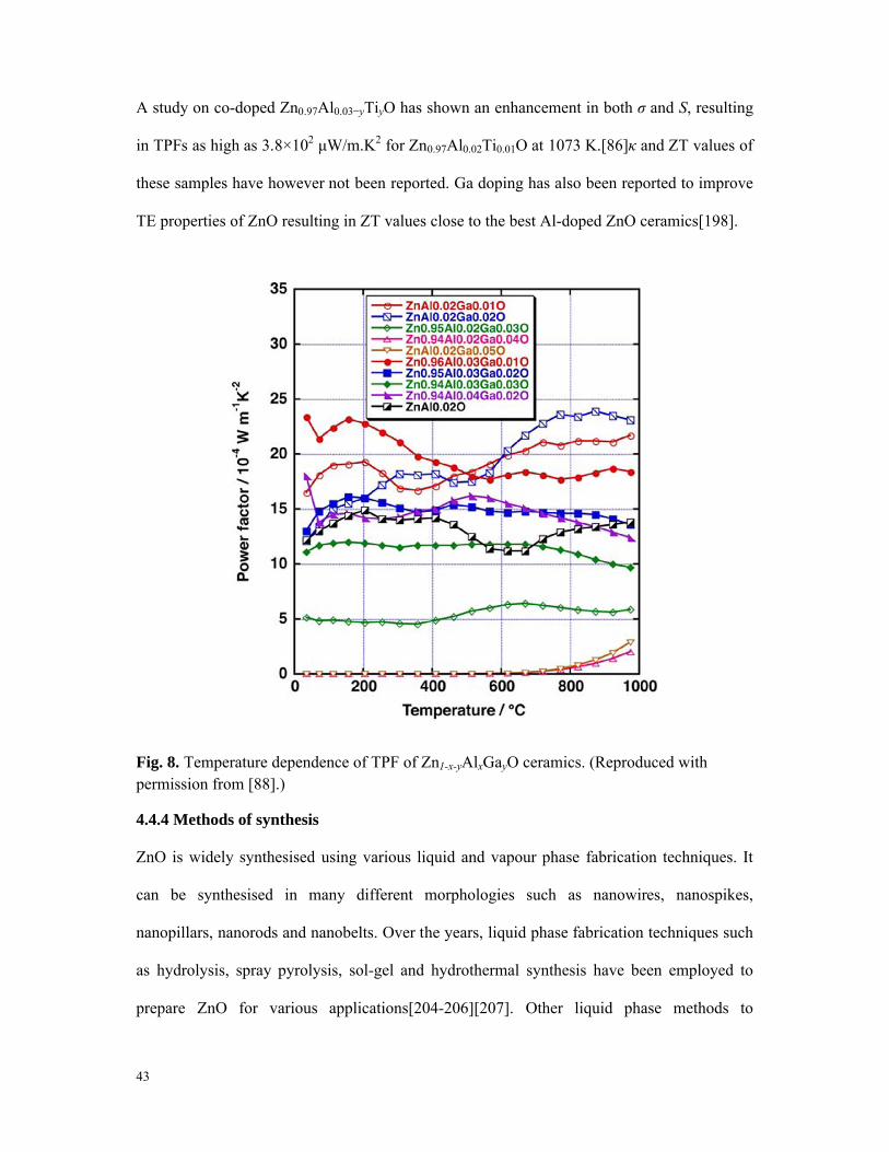
43
A study on co-doped Zn0.97Al0.03−yTiyO has shown an enhancement in both σ and S, resulting
in TPFs as high as 3.8×10² μW/m.K2 for Zn0.97Al0.02Ti0.01O at 1073 K.[86]κ and ZT values of
these samples have however not been reported. Ga doping has also been reported to improve
TE properties of ZnO resulting in ZT values close to the best Al-doped ZnO ceramics[198].
Fig. 8. Temperature dependence of TPF of Zn1-x-yAlxGayO ceramics. (Reproduced with permission from [88].)
4.4.4 Methods of synthesis
ZnO is widely synthesised using various liquid and vapour phase fabrication techniques. It
can be synthesised in many different morphologies such as nanowires, nanospikes,
nanopillars, nanorods and nanobelts. Over the years, liquid phase fabrication techniques such
as hydrolysis, spray pyrolysis, sol-gel and hydrothermal synthesis have been employed to
prepare ZnO for various applications[204-206][207]. Other liquid phase methods to

44
synthesise highly crystalline ZnO nanostructures include electrochemical techniques such as
anodization and electrodeposition[208, 209].
Vapour deposition techniques such as RF/DC sputtering, ALD and MBE as well as chemical
vapour deposition (CVD) technique and metal organic chemical vapour deposition
(MOCVD) have been used to synthesise pure as well as doped ZnO thin films[210-
213].Other techniques such as spark plasma sintering (SPS)and PLD have alsobeen widely
used to synthesise densified ZnO in a powdered form[170][214, 215].
4.5 Copper oxides– Cu2O and CuO
4.5.1 Crystal structure
Copper oxide occurs in two common phases:cuprous oxide (Cu2O) and cupric oxide
(CuO).Cu2O (copper(I) oxide) has been commonly used for application in solar
cells,catalysts, and sensors[216]. It exhibits a cubic crystal structure with a forbidden direct
bandgap of ~1.9-2.2 eV, making it very challenging to study quantum confinement effects or
modify its properties[217, 218]. Cu2O has also been shown to depart from stoichiometry
towards excess oxygen, leading to a p-type semiconducting natureand has been one of the
most studied materials in semiconducting physics[219].On the other hand, CuO (copper(II)
oxide) belongs to the monoclinic crystal system with a direct bandgap of 1.2-1.5 eV and has
been studied for photoconductive applications and is also the basis for several high
temperature superconductors[217, 220].In CuO, each Cu atom is coordinated by 4 oxygen
atoms in an approximately square planar configuration. In a pure state and good
stoichiometry, CuO behaves almost like an electrical insulator. However, non-stoichiometry
leads to important semiconducting characteristics[221].
45
4.5.2 TE properties of stoichiometric copper oxides
A limited number of studies have been carried out on the TE properties of copper oxides in
the 1990s. Jeong et al. examined the S and σ in uniaxially pressed CuO powder, which was
subsequently sintered at different temperatures[222]. The CuO sample sintered at 1273 K in
air, showed a peak S of ~650 μV/K between 400 to 500 K. Beyond 500 K, the S dropped
rapidly. The corresponding σ as seen from Fig. 9a was approximately 1 S/m, resulting in a
TPF of 0.42 μW/m.K2[222].
It has been shown that single crystal Cu2Oexhibits a high S at elevated temperatures
(~1050 μV/K at 923 K)[219].On the other hand, the S of CuO thin films has been shown to
change with varying film thicknesses (340 nm to 620 nm) and exhibits a maximum value of ~
500 μV/K for ~600 nm thick films (Fig. 9b)[221]. However, none of these works reported
electrical or thermal conductivities. The full TE properties of intrinsic copper oxides are yet
to be investigated.
4.5.3 TE properties of non-stoichiometric,doped and composite copper oxides
The doping technique has been shown to result in significant effect on the TE properties of
copper oxides. Koffyberg et al. have demonstrated the TE effect in polycrystalline samples of
Li doped CuO[223]. They have shown an average p-type S of 770 μV/K and σ of 6.25 S/m,
resulting in a TPF of 3.7 μW/m.K2[223].
It seems that the most commonly investigated copper oxide composite for its TE properties is
La2CuO4. It exhibits a simple layered structure comprising of 2D CuO2 planes in a unit cell
andis the parent compound for high temperature superconductivity, whichis related to the
excess oxygen content and the structural change as a result of phase transition[224]. This
layered structure makes the anisotropy of conduction very strong. Due to the anisotropic

46
nature of their electrical conduction, such composites are potential TE materials. A detailed
overview of its crystal phases is provided elsewhere[225].
For enhancing the TE properties of La2CuO4 metallic dopants can be incorporated.In this
regard, TE properties of La2-xRxCuO4 polycrystalline ceramics, where R can be Pr, Y or Nb
have been investigated[226]. In this study, it has been shown that the choice of dopants plays
a crucial role in determining the TE properties. Fig. 9c shows the variation of the TPF of La2-
xRxCuO4with temperature for different dopants. As can be seen, withincreasing temperature
the TPFs of all composites decrease, eventually becoming stable above 700 K[226]. Samples
show S ranging between 200 to 620 μV/K. Amongst them La1.98Y0.02CuO4 ceramics exhibit a
high TPF of 103 μW/m.K2. The maximum ZT was reported to be 0.17 at 330 K, which is
around 3 times higher than pure La2CuO4[226].
Studies on TE properties of n-type RE2CuO4 oxides, where RE is a rare earth element such as
neodymium, samarium or gadolinium,have shown TPFs and ZTsof the order of 10 μW/m.K2
and 0.005, respectively, at 950 K[227]. The electrical resistivities of such composites show a
negative temperature dependence and is at least a magnitude higher than many conventional
TE materials. Such RE2CuO4type oxides exhibit a highκof ~30 W/m.K at 300 K, which
dropsto ~ 8 W/m.K at 950 K[227], and can potentially be suitable for thermopower wave
applications.
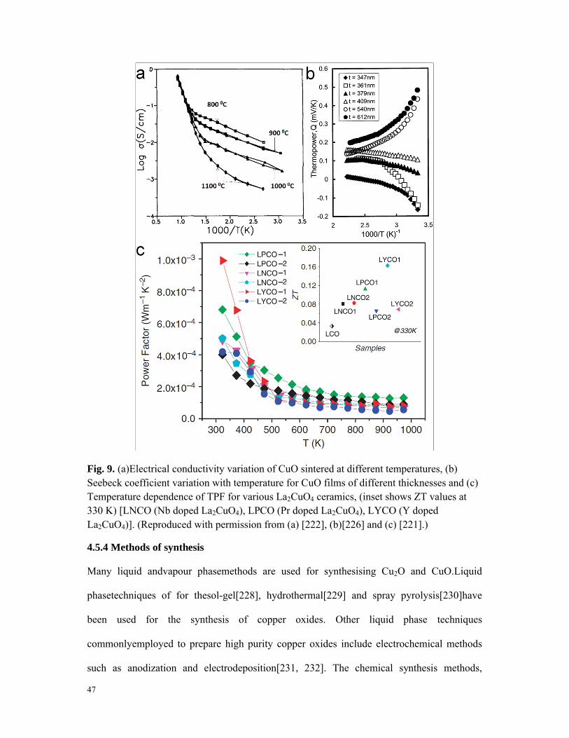
47
Fig. 9. (a)Electrical conductivity variation of CuO sintered at different temperatures, (b) Seebeck coefficient variation with temperature for CuO films of different thicknesses and (c) Temperature dependence of TPF for various La2CuO4 ceramics, (inset shows ZT values at 330 K) [LNCO (Nb doped La2CuO4), LPCO (Pr doped La2CuO4), LYCO (Y doped La2CuO4)]. (Reproduced with permission from (a) [222], (b)[226] and (c) [221].)
4.5.4 Methods of synthesis
Many liquid andvapour phasemethods are used for synthesising Cu2O and CuO.Liquid
phasetechniques of for thesol-gel[228], hydrothermal[229] and spray pyrolysis[230]have
been used for the synthesis of copper oxides. Other liquid phase techniques
commonlyemployed to prepare high purity copper oxides include electrochemical methods
such as anodization and electrodeposition[231, 232]. The chemical synthesis methods,

48
especially hydrothermal are much desired for many applications as they are low cost, offer
morphology control and facilitate low temperature synthesis and are therefore viable for large
scale production[229]. Additionally, they result in a departure from stoichiometry when it is
needed due to the introduction of point defects and impurities in the crystal lattice. Vapour
phase techniques such as RF sputtering, PLD, various evaporation approaches and MBE have
been demonstrated to synthesise crystalline copper oxide thin films at different oxygen
contents[220]. Additionally, the CVD technique has also been utilized to synthesise copper
oxides[233].
In most copper oxide synthesis methods a mixture of phases like Cu, Cu2O and CuO is
obtained. Post-deposition annealing or deposition at high temperature is usually needed to
achievethe desired phase.

49
4.6 Vanadium oxides
4.6.1 Crystal structure
Vanadium oxide existsin many phases that include VO, VO2, V2O3 or V2O5. However, only
V2O5 demonstrates TE properties and shows highly anisotropic n-type electrical
conduction[234]. It has a direct bandgap of ~2.4 eV and is a promising electrode material for
energy storage systems such as Li-ion batteries[235-238] and possesses a high ionic storage
capacity because of its layered structure[239]. Over the years, it has also been intensely
investigated for its electrochromic properties[240, 241]. Unlike other configurations of
vanadium oxide that have been known to exhibit multiple crystal phases, V2O5 exists only as
anorthorhombic crystal, which is fundamentally comprised of VO5 pyramids that form
alternating double chains along the b-axis[242].A detailed overview of the crystal structures
of all phases of vanadium oxide is provided elsewhere[242].
4.6.2 TE properties of stoichiometric V2O5
Kounavis et al.have demonstrated that V2O5 gels exhibit a room temperature TPF of
0.3 μW/m.K2[243]. V2O5 films synthesised by sol-gel method exhibitS of ~–200 μV/K, but
have very high resistances of the order of 103 to 104Ω[239]. Hence, it is evident that the σ of
V2O5 films requires significant enhancement for practical refrigeration and energy
scavenging applications.
4.6.3 TE properties of nanostructured,doped and composite V2O5
Bahgat et al.have synthesized highly oriented nanocrystalline, hydrated vanadium pentoxide,
(V2O5.nH2O) films of 200 nm thickness. The S and σ of such films have been shown to
increase with temperature, resulting in a peak TPF of 101.25 μW/m.K2 at 480 K(Fig. 10a &
b)[244].

50
Iwanaga et al.have studied the TE properties of V2O5 thin films and reported that the
introduction of metallic dopants (Na in this case)can improve the TPFvalues dramatically.
This is primarily due to an increase in σ by a factor of up to ~ 104. At the same time, the S
reducesto almost half itsvalue. The direct measurements of TPFhave shown an enhanced TPF
of 10 μW/m.K2 (compared to ~10–2 μW/m.K2 for pure V2O5 films) for 35 % Na doping[245].
Liu et al.have shown that polyethylene oxide (PEO) intercalated layered V2O5 xerogel
nanocomposites result in low TPFs.[246] PbO and ZnO based vandates have also been shown
to exhibit S of up to –400 μV/K at room temperature[247]. However, σ in such composites is
low, so they can possibly be used only in temperature sensors.
Fig. 10. Temperature dependence of (a) electrical conductivity, (b) Seebeck coefficient for the as-cast and heat treated films during heating and cooling cycles of hydrated V2O5. (Reproduced with permission from [244].)
4.6.4 Methods of synthesis
V2O5 films can be synthesised using various liquid and vapour phase
techniques[248].Commonly used liquid phase methods for the synthesis of V2O5 thin films
are the sol-gel and the hydrothermal synthesis technique in which hydrated forms are
obtained. The sol-gel synthesised hydrated nanocrystalline V2O5has been shown to exhibit

51
the highest TPF[244]. A melt quench technique has also been employed to dope various
concentrations of Na+ ions into sol-gel solutions and subsequently, thin films of Na
intercalated V2O5 can be prepared[243, 245]. Hydrothermal synthesisis often utilized to
synthesise V2O5 nanostructures such as nanotubes and nanowires[249, 250].Other liquid
phase methods include the electrodeposition and anodization techniques which have also
been shown to synthesise V2O5 nanostructures[251-253].
Vapour phase techniques such as RF sputtering[254], ALD[255] and PLD[256]have also
been shown to deposit crystalline V2O5 thin films of various phases. Additionally, the CVD
method has also been demonstrated to form highly crystalline V2O5 thin films[257].
However, there are few reports on the TE properties of V2O5 prepared using vapour
deposition techniques.

52
4.7 Cobalt oxides
4.7.1 Crystal structure
Cobalt oxide based materials have received great attention for their application in gas
sensing, heterogeneous catalysts, intercalation compounds for energy storages,
electrochromic devices and more recently asTE materials [258, 259]. Cobalt oxides
aregenerally found in twostable oxide compounds: Co3O4 and CoO. Co3O4 is the morestable
of these two. Both Co3O4 and CoO exhibit a cubic lattice. Co3O4 is a spinel with the presence
of both Co2+ and Co3+ ions in its lattice. Co3O4 exhibits a bandgap in the range of 1.4-1.8 eV,
while CoO has ahigher energy bandgap of 2.2-2.8 eV. Both Co3O4 and CoO are usually non-
stoichiometric with excess oxygen, leading to p-type semiconducting behaviours[259].
4.7.2 TE properties of stoichiometric cobalt oxides
So far, the TE properties of pure cobalt oxides have not been investigated widely, mainly due
to the fact that high resistivities result in a poor TE performance for many energy scavenging
applications. It has been shown that in a bulk form CoO exhibits a TPF of ~ 80 μW/m.K2 at
1000 K[260]. However, the use of various approaches suggested in section 3 such as the
addition of metallic dopants, substructuring, and reducing the dimensionality have made
doped cobalt oxides the best TMOs for various TE applications.
4.7.3 TE properties of non-stoichiometric, doped, composite and nanostructured cobalt
oxides
Rare-earth cobalt oxides (RECoO3) with perovskite crystal structures have been studied for
their TE properties for energy scavenging and cooling properties and have shown relatively
large figure of merits around the room temperature[82]. Their high-temperature performance
is however limited.
P-type cobalt oxide composites are among the TE metal oxides with the largest ZT values
reported todate. The most promising cobaltite composites for such TE applications are

53
NaxCoO2 and Ca3Co4O9[78].The high ZT values are associatedwiththeir crystal
structures,which consist of CoO2- planes composed of edge-sharing CoO6 octahedra, and
other structural components between these layers. NaxCoO2 exhibits a weak monoclininc
distortion with respect to the hexagonal unit cell caused by the ordering of a layer of sodium
ions in between CoO2 planes, while Ca3Co4O9 comprises of a distorted rock-salt type layer of
Ca2CoO3, which lowers thermal conductivity by shortening the phonon mean free path (Eq.
2a), and is located between two CdI2 type CoO2 layers that are mainly responsible for
providing the path for electrical conduction. Hence, these composites are a classic example of
substructuring, which is predicted to enhance TE performance (section 3.2).
Terasaki et al.are the pioneers of layered cobalt oxide base TE materials. They were the first
group to demonstrate large TPFs of the order of 5×10³ μW/m.K2 (compared to
4×10³ μW/m.K2 for Bi2Te3) and ZT as high as 0.75 in NaCo2O4 single crystals at room
temperature[11]. Fig. 11a & b show the variation of resistivity and S with temperature for the
NaCo2O4 single crystals[11].Subsequent studies have shown that
polycrystallineNaxCoO2exhibits TPF as high as 1.4×10³ μW/m.K2for x = 0.85 at room
temperature[261, 262]. For NaxCoO2, silver (Ag) doping results in the enhancement of
ZT[78]. Other metallic dopants such asCu[95] and Zn[96]have also been shown to increase
the TPFs, while Sr doping results in the improvement of ZT[263].PolycrystallineNaxCoO2
typically shows a peak ZT of ~0.11. However, recently, two-dimensional (2D) and stacked
NaxCoO2 nanostructures prepared by exfoliation/restacking method were reported to exhibit
enhanced TE properties for energy scavenging applications, as expected from the discussion
insection 2[264, 265]. The enhancement was attributed to the reduction of in-plane and cross-
plane thermal conductivities in the super-lattice like structures, resulting in enhanced TPFs
and ZTs of approximately 500 μW/m.K2 and 0.4, respectively.

54
On the other hand, undoped Ca3Co4O9exhibits σ, S, κ, TPF and ZT of 104 S/m, 150 µV/K,
2 W/m.K, 225 μW/m.K2 and 0.3,respectively, at elevated temperatures as large as 1000 K.
Although, the room temperature TPFs performance of Ca3Co4O9is inferior to NaxCoO2, it is
more commonly used in various TE applications due to its superior stability to compositional
changes and better performance at high temperatures[78].
Similar to NaxCoO2, the addition of Ag as a dopant[266, 267] or a second
phasecomposite[266, 268, 269]has been shown to improve TE properties of Ca3Co4O9. A
Ca2.7Ag0.3Co4O9/Ag-10 wt% composite showed an enhancedZT of 0.5 at 1000 K. Bismuth
(Bi) dopinghas also resulted in enhancedTPFs and reducedκ. However, the ZT of Bi-doped
samples, is not as high as those of Ag doped oxides.Ca2.75Gd0.25Co4O9 ceramics have also
been shown to exhibit TPF and ZT of 480 μW/m.K2 and 0.23 respectively, at 923 K (Fig.
11c)[270].It is seen that the Ca2.75Gd0.25Co4O9ceramics synthesised using the SPS method
exhibit slightly higher TPFs and ZTs compared to hot press (HP) synthesised samples (Fig.
11c).There are also reports on the doping of Ca3Co4O9 with transition metals[271, 272] such
as copper and nickel. Gallium addition has been demonstrated to improve TPFs and
ZTs[273]. Doping with lanthanum and lanthanide elements has also been studied but the TE
enhancements have notbeen as impressive[78].

55
Fig. 11. (a)Resistivity and (b) Seebeck coefficient variations with temperature for NaCo2O4
single crystals in plane (ρa) and out of plane (ρc) and (c) comparison of ZT and TPF for SPS and hot pressed (HP) synthesised Ca2.75Gd0.25Co4O9 samples. (Reproduced with permission from (a), (b) [11] and (c) [270].)
4.7.4 Methods of synthesis
Cobalt oxide can be synthesised using various liquid and vapour phase methods. Epitaxial
thin films are generally preferred as they result in highly oriented structures[1, 274, 275].
Liquid phase techniques such as spray pyrolysis, sol-gel and hydrothermalhave been
employed to fabricate cobalt oxide thin films as well as nanostructures in various
morphologies such as nanorods, hierarchical nanocolumns, nanocubes, nanowires and
nanorods [258, 276-278]. Although, other liquid phase methods such as electrodeposition
have also been employed[279]. An excellent review article summarises various liquid phase
synthesis techniques for fabricating cobalt oxide nanostructures[278].
Vapour phase methods that include MBE, PLD and EBEhave conventionally been used for
the growth of epitaxial Ca3Co4O9 films.For NaxCo2 films however, the volatility of sodium
ions poses difficulties in controlling stoichiometry. The CVD synthesis technique has been
shown to be advantageous since it allows accurate tailoring of system composition, structure,
morphology via suitable choice of a precursor compoundsand deposition conditions[258].

56
4.8 Rhodium oxides –RhOx
4.8.1 Crystal structure
Rhodium oxidesare generally found in two crystal oxide compounds: RhO2 and Rh2O3.RhO2
exhibits a tetragonal rutile structure,which transforms into corundum type α-
Rh2O3afterannealingabove 1000 K[280].Heating abovesuch temperatures results in a
transformation to orthorhombic type β-Rh2O3[281]. Rhodium oxides have been investigated
primarily for applications in catalytic chemistry, electrochromisms and as a conductive
transparent oxide[282-284].Additionally, misfit-layered rhodium oxides with two-
dimensional CdI2-type crystal structures, analogous to that of cobalt oxides, are among the
best candidates for forming p-type TE materials[59]. As in the case for cobalt oxides, their
superior thermopower properties originate from CdI2-type layers, which favour low spin state
of Rh3+/ Rh4+ with degeneracies of spin and orbital as the key factors[285]. The CdI2-type
layer has a hexagonal symmetry, while the misfit layer is generally a square lattice. However,
a layered Bi-Sr-Rh-O system with fluorite-type misfit layers with a trigonal symmetry has
also been reported to exhibit similar TE properties[59].
4.8.2 TE properties of stoichiometric RhOx
There are no reports ofstoichiometric RhOxbeing employed in TE systems. What follows is a
brief overview of the studies on rhodium oxide based metal oxide systems that are among the
best p-type TE TMOs.
4.8.3 TE properties of non-stoichiometric,composite and doped RhOx
Okada et al. initially reported the first synthesized misfit-layered rhodium based metal oxide
in polycrystalline form[286]. Samples of (Bi1-xPbx)1.8Sr2Rh1.6Oy (x=0, 0.1, 0.2) and
Bi1.8Ba2Rh1.9Oy were investigated for their TE properties, with the most promising results
being 125 µV/K, 213 S/m and 3.3 μW/m.K2 for S, σ and TPF, respectively, at room
temperature(see Fig. 12a-c). In another study, polycrystalline samples of Co and Rh mixed
57
solutions Bi1.7Ba2(Co1-zRhz)Oy with hexagonal (Co, Rh)O2 layers have been synthesized in an
effort to further alter the TE properties by decreasing κ[287]. Although κ was reduced in the
solid solution, the σ also dropped due to the distortions made by different ionic size elements
in (Co, Rh)O2 layers and therefore, TE performance did not improve.
Kobayashi et al.have synthesized rhodium oxide based single crystals in Br-Sr-Rh-O systems
with alternately stacked conductive RhOx and insulating in (Bi0.75Sr0.25)O1.5 fluorite-type
layers[59]. Interestingly, the misfit layer showed a trigonal symmetry with a rhombohedral
unit cell, rather than the square-lattice usually observed in other oxides. Room temperature S
of up to 63 µV/K and σ of 6.25×10⁴ S/m were obtained for Bi0.78Sr0.4RhO3+y crystals. The
TPF of such a compositewas estimated to be 248 µW/m.K2, which is comparable to the
values for cobalt oxide based systems[59]. Additionally, single crystals of Ba1.2Rh8O16 have
been shown to exhibit κ and ZT values of 3 W/m.K and 0.02 at 200 K, respectively[288].
A recent first principle investigation of layered KxRhO2composites based on ab-initio
calculations and Boltzmann transport theory has suggested that the material system has the
potential for exceptionally remarkable TE properties[289]. Calculations found large Seebeck
coefficients in the temperature range of 0 to 700 K for hydrated phase of KxRhO2. Moreover
a peak value of ZT = 0.3 is predicted for K7/8RhO2 at 100 K, which is higher than NaxCoO2
systems. Even at room temperature, TPFs higher than NaxCoO2 are predicted[289].

58
Fig. 12. Temperature (T) dependence of (a) resistivity (ρ), (b) Seebeck coefficient (S), and (c) thermal conductivity (κ) for Bi1.7Ba2(Co1−zRhz)Oy of varying rhodium concentration (z) (Reproduced with permission from [287].)
4.8.4 Methods of synthesis
Many liquid and vapour phase techniques are employed to synthesise rhodium oxides.
Amongst the liquid phase synthesis techniques, sol-gel and hydrothermal are the most
commonlyused methods to synthesise Rh2O3in various morphologies[290-292].Vapour phase
techniques such as RF sputtering, electron beam evaporation (EBE) and the CVD method are
used for preparing crystalline rhodium oxide thin films[293].Misfit, layered rhodium oxide
composites such as (Bi1-xPbx)1.8Sr2Rh1.6Oy are synthesised using the SSR technique[286,
287].It should be considered that RhO2 is insoluble even in hot aqua regia, hence solution
based synthesis techniques are not employed for forming RhO2. SSR is therefore commonly
utilised[294].

59
4.9 Molybdenum oxides –MoOx
4.9.1 Crystal structure
The most common stoichiometries of MoOx are MoO2 and MoO3. However, MoO3 is the
most widely investigated stoichiometry of MoOx for a variety of applications such as gas
sensing, photochromic devices, light emitting diodes (LEDs), batteries and organic solar
cells[238, 295-302].The most common crystal phases of MoO3 are the thermodynamically
stable α-MoO3 and the metastable β-MoO3[303-306]. Bulk α-MoO3exhibits an indirect
bandgap of ~3 eVandhas an orthorhombic crystal structure,that comprises of dual layered
planar crystals of distorted MoO6 octahedra that are held together by weak van der Waals
forces. β-MoO3 on the other hand comprises of MoO6 octahedra that share corners in all the
three dimensions, resulting in a monoclinic 3D structure[302, 307].At temperatures above
620 K, the β phase transforms into the more stable, layered α-MoO3 phase[303, 304].
4.9.2 TE properties of stoichiometric MoOx
There is no literature that reports the TE properties of stoichiometric molybdenum oxides,
primarily due to their low σ. However, incorporation of various dopantsand implementation
of MoOxcomposites have been shown to result in high TPFs.
4.9.3 TE properties of non-stoichiometric, doped and composite MoOx
Non-stoichiometric and doped molybdenum oxides have been shown to exhibit high TPFs.
Xu et al. investigated the TE properties of highly reduced molybdenum oxides (RMo8O14)
where R=La, Ce, Nd and Sm. Fig. 13a shows the TPFs of the fourcomposites atdifferent
temperatures. It is seen that NdMo8O18 exhibitsapeakTPF and ZT of 177 μW/m.K2 and 0.1,
respectively, at 1000 K. The κof the compositehas been reported to be 3.19 W/m.K at 322 K,
whichdrops to 2 W/m.K at 1164 K[308, 309].It is evident that the TPF is certainly large
enough to make these molybdenum oxide composites promising for high temperature energy
scavenging applications.

60
It has also been shown that the use of composites can result in enhanced TE performance as
suggested in section 3.4. A study reports that the TPFs of polyaniline (a typical conductive
polymer) molybdenum trioxide (PANI/MoO3) composites,is high. A maximum TPF of
~102 μW/m.K2was observed for 10 wt% of MoO3(Fig. 13b)[310].
Fig. 13. (a) Temperature dependence of TPF of RMo8O14 (R:La, Ce, Nd, Sm) pellets, and (b) electrical conductivity vs TPF of PANI/MoO3 composites vs MoO3 concentration in the composite. (Reproduced with permission from (a) [309] and (b) [310].)
4.9.4 Methods of synthesis
Similar to other TMOs, MoO3 can be synthesised using many different liquid and vapour
phase techniques. The commonly used liquid phase techniques include sol-gel, hydrothermal,
and electrodeposition[304]. Vapour phase techniques such as thermal evaporation, electron
beam epitaxy, PLD, RF/DC sputtering, MBE and van der Waal epitaxy (VDWE) have been
used for synthesising MoO3 in various thin film and nanostructured forms. Amongst these,
MBE and VDWE have been shown to synthesise ordered, layered MoO3 structures.
Additionally, CVD techniquesare also employed to synthesise crystalline MoO3. A detailed
overview of the synthesis techniques to produce various morphologies of MoO3 is provided
elsewhere[302].

61
4.10 Other transition metal oxides and their TE properties
In this section, we will discuss other TMOs, whose TE properties have not been widely
investigated. Most of these TMOsare wide bandgap materials, resulting in extremely poor
electrical conductivities. However, a few oxides such as iron oxide, cadmium oxide, nickel
oxide and doped zirconium oxide exhibit promising TE properties for various applications. In
this section, we provide a brief overview of the small number of reports on the TE properties
of the remaining TMOs in their stoichiometric and/or doped states.
4.10.1 Iron oxides
There are many known stable iron oxide stoichiometries available. Amongst them, Fe2O3is
the iron oxide compound that has been studied for its TE properties.An analysis ofa limited
number of reports suggests that Fe2O3 can potentially be a promising TMO for TE
applications at high temperatures as it exhibits high TPFs at room as well as elevated
temperatures
Fe2O3 thin films have been shown to exhibit peak S of 1650 μV/K in the temperature range of
270-290 K. A peak σof 5.5×10³ S/m has been reported in the same temperature range,
resulting in a high TPF of 1.5×10⁴ μW/m.K2[311].Li- doped α-Fe2O3has been reported to
exhibit a TPF of 5.5×10³μW/m.K2 at temperature over 800 K for which a κ of 4 W/m.K has
been reported[312]. Fe2O3-NiO compositeshave also been shown to exhibit high TPFs at
elevated temperatures(900 μW/m.K2 at 823 K)[313].Nanostructuring technique has been
predicted to enhance TE performance(section 3.3). Although, 1D electronic quantum
confinement has been demonstrated in α-Fe2O3 nanorods, they have not been examined for
their TE properties[314].

62
4.10.2 Chromium oxides
There exists many crystalline phases of chromium oxides however, Cr2O3 is the most stable
bulk form of this TMO,[315]with a few recent reports on its TE properties[311, 316].
Cr2O3thin films have been shown to exhibit S of 3500-4500 μV/K at room
temperature.However, we wish to add that such dramatically high S has not been confirmed
by any other study so far. A σof 5.8×10³ S/m has been reported for stoichiometric
Cr2O3[311].Another study demonstratesa TPF of 3.5 μW/m.K2 at a temperature of 1300 K in
Cr2O3[316].
The effect of TiO2 addition to Cr2O3 on its TE properties has also been investigated. A 2 %
TiO2 addition results in a slightly improved TPF of 5.6 μW/m.K2[317].
The TE properties of chromium oxide compoundssuch as CuCrO2have also been studied.A
maximum TPF and ZT of 236 μW/m.K2 and 0.1 at 1100 K has been
obtained[318].CrO0.1N0.9 polycrystalline samples have also been reported to show a TPF of
80 μW/m.K2 at 300 K[319].
The above discussion shows that sufficiently large TPFs have been demonstrated for Cr2O3
and its compounds. However, further studies are required to establish chromium oxide as a
viable TE TMO for many applications.
4.10.3 Scandium oxides
Scandium oxide is a wide band gap (6 eV) insulating material, and is therefore not useful for
TE conversion applications[118]. Doping can slightly improve electrical conduction;
however, it is still insufficient for any meaningful TE energy scavenging applications. Cu
doped scandium oxide epitaxial thin films exhibit S and σof 40 μV/K and 110 S/m,
respectively, at room temperature, resulting in extremely low TPF of 0.18 μW/m.K2[320].

63
4.10.4 Zirconium oxides
Zirconium oxidesare stable at extremely high temperatures and are generally used as ionic
conductors at such temperatures. As such these oxides are frequently used in oxygen sensors
and fuel cell membranes[321].ZrO2 is the most common crystal phase of zirconium oxides
which is found in three phases: a cubic phase with a fluorite structure that occurs at
temperatures >2850 K and transforms into a tetragonal phase at 2650 K, which on further
cooling transforms to a monoclinic phase[322]. It exhibits a wide bandgap of 5 eV[118].
Pure ZrO2 does not exhibit good TE properties due to its poor σ. However, ZrO2/CoSb3
nanocomposites show a peak S of 140 μV/K at 700 K for 5 % ZrO2 and a corresponding σand
κ of3.75×104 S/m and 2.75 W/m.K,respectively[114].The resulting TPF and ZT is
approximately 735 μW/m.K2 and 0.2, respectively. Therefore, it is obvious that the
incorporation of ZrO2 can potentially be a good approach for obtaining enhanced TE
properties for energy scavenging at elevated temperatures.
4.10.5 Cadmium oxides
Cadmium oxide is an n-type semiconductor, which exhibits a cubic rocksalt type crystal
structure with a direct bandgap of ~2.1 eV at room temperature[323]. A study of highly
crystalline CdO thin films have revealed high σ of the order of 105 S/m and a peak S of –
90 μV/K, resulting in a high TPF of ~800 μW/m.K2[324]. Another studyhas demonstrated a
TPF of 100 μW/m.K2 at 700 K[325]. Other studies on pure as well as doped CdO have
revealed similar order of magnitude TPFs[326-328]. Therefore, it is evident that CdO can
potentially be a viable n-type TE TMO at elevated temperatures.
4.10.6 Nickel oxides
Nickel oxide is a p-type semiconductor that exhibits a cubic rocksalt type crystal structure
with a rather large bandgap of 3.6-4.0 eV. Although the σ of stoichiometric NiO is extremely

64
low, Ni2+ vacancies are easily formed in undoped NiO, resulting in dramatic improvements in
σ[329].
In the past, a few studies have examined TE properties of NiO[330, 331]. One such
studyhasreported S, σ of 101 μV/K and 10–2 S/m respectively, at room temperature. The TPF
is extremely low primarily due to poor electrical conductivity[331].
The use of metallic dopants such as Li and Na has been shown to result in enhanced TE
properties[332][333]. Li doped NiO exhibitsTPFs of the order of 102 μW/m.K2at
temperatures exceeding 1000 K, suggesting its suitability as a promising metal oxide for
energy scavenging and thermopower wave sources[332].
4.10.7 Iridium oxides
IrO2 is the most stable phase of iridium oxidesand exhibits a TiO2 like rutile crystal structure.
The TE properties of pure IrO2 have not been examined. However, Ca-Ir-O composites have
been investigated for their TE properties by Keawprak et al[334-336]. They reported low
TPFs and ZTs(~35 μW/m.K2 and 0.01, respectively).
4.10.8 Other TMOs
Other transition metals such as Nb, La, Ac Y, Ta, Re, Hf, Ag and Te are usually employed as
dopants in other TE TMOs for tuning their various TE properties in order to achieve higher
TPFs and ZTs. However, reports on their stoichiometric TMOs are rare and yet to be fully
investigated.

65
5Applicationsof TE TMOs
As discussed in Section 3, the applications of TE TMOs can be classified into four major
categories. In this section, a brief description of such TMO-based TE applications is
provided.
5.1 Cooling and refrigeration
One of the practical implementationof TE materials is for cooling and refrigeration[3].TMOs
generally do not provide considerable efficiencies for cooling and refrigeration near room
temperatures. However, many of them including titanium oxide, copper oxide compounds
(La2CuO4) and doped cobalt oxides, are promising for cooling and refrigeration applications
at low temperatures due to their large TPFs at cryogenic temperatures[337, 338]. The
advantage of TMO-based cooling and refrigeration systems is their low cost and easy large-
scale fabrication.Many TMOs can be synthesised in low dimensions, using well-established
methods which were presented in Section 4,making them attractive for developing
micro/nano cooling devices[339].A schematic of such cooling devices is shown in Fig. 14,
and consists of complementary arrays of n-type and p-type TE TMOs, which are electrically
in series and thermally in parallel, transferring heat from one side of the module to
another[261]. The need for micro-domain cooling is driven largely by the shrinking size of
electronic devices.Most electronics and optoelectronic technologies require localised spot
cooling of small components and TE modules are capable of very localised
cooling[261].Such modules are extensivelyused for maintaining laser diodes at constant
temperatures in order to stabilise their operating wavelengths[340, 341].They are also widely
used for the temperature management of high power dissipating electronic equipment such as
ICs, microprocessors, charge coupled devices (CCD), IR cooling in optoelectronic systems,
air conditioners and laboratory cooling plates[67, 342, 343].Additionally, a reversal of the

66
current allows these devices to act as spot heaters as well, rendering them with additional
usage flexibility[344].
Military applications such as night vision systems and heat seeking missiles depend on
sensors in their infrared imaging systems. These sensors work efficiently at extremely low
temperatures. TE TMO based cooling systems can be used to produce suchlow temperatures
of the order of ~190 K in these devices[67, 345].Suchcooling devices are also increasingly
finding applications in the biological world. For a wide cryogenic implementation in the
biological world, TMOs due to their non-toxicity and biological compatibility are potentially
desirable.
Fig. 14.Pictorial representation of a TE cooling device. (Reproduced with permission from [261].)

67
5.2 Energy harvesting from heat
The application of TMOs for waste heat recovery is particularly attractive, given their
stability at very high temperatures,even though the maximum theoretical efficiencies for
TMOs in the high temperature regimes is in the range of 4-6%[346].Complex oxides such as
p-type layered cobaltites and n-type doped SrTiO3, CaMnO3 and ZnO are among the best
candidates for TE power generation modules operating at mid to high temperature ranges[12,
347, 348]. Among these, p-type Ca3Co4O9 (either undoped or doped with bismuth) and n-type
doped CaMnO3 are commonly used in TE modules. TMO TE modules are being increasingly
employed for waste heat recovery in vehicles by all major auto-makers in order to comply
with stricter emission requirements[78, 349]. SuchTE generators convert the waste heat from
the exhaust into useful power that can be used to operate the on-board electrical systems,
thereby increasing fuel efficiency[4]. Each kilogram of fuel saving reduces CO2 emissions by
3.16 kg. Additionally, the application of TMO TE modules in the industrial waste heat
recovery sector is also gaining increasing attention due to the tremendous economic and
environmental benefits that can be realised especially in the aluminium smelting, glass
manufacturing and cement production industries.
The first prototypes of power generation modules incorporating TMOs were reported by Shin
et al. in whichan output power of 14 mW was measured at a temperature gradient of 500 K
(1000 K on the hot side and 500 K on the cool side) and the efficiency was calculated to be
0.64%[350, 351].All-oxide TE modules were later developed by Matsubara et al. and
Funahashi et al. that generated output powers as large as 94.4 mW[352, 353]. Subsequently,
using the same p- and n-type oxides Funahashi et al.fabricated a module comprising of 140
oxide pairs on an alumina substrate resulting in an output power of 0.15 W with a
temperature gradient of 551 K[354]. The power generation efficiency was estimated to be
around 1.4%. A further improvement in the output power (0.28 W) was achieved through the

68
fabrication of a pipe-shaped module comprising 54 oxide pairs.[355]. Another plate-shaped
module fabricated using 8 pairs of p-type Co-394 and n-type CaMn0.98Mo0.02O3 (Mn-113)
bulks on alumina substrate reached an output power of 0.34 W[356]. Other studies with
cobalt and manganese based oxides have resulted in output powers of the same order[357-
360].
The nanostructuring approach has also been implemented to improve the performance of
TMO based TE modules. Such modules use nanostructured p-type cobalates, manganates or
n-type ZnO andhave been shown to generate powers as high as 0.4 W[361-363].
5.3 Photovoltaic (PV)–solar thermoelectric generators(STEGs) andradioisotope thermoelectric generators (RITEGs)
5.3.1 PV-STEG
Photovoltaic cells are widely deployed to harness solar energy and convert it to useful
electrical energy. An interesting idea to improve the efficiency of these cells is the
incorporation of TE devices, also known as solar thermoelectric generators (STEGs). These
TE-solar hybrid systems can take advantage of the IR part of the solar spectrum, which is not
effectively captured by conventional solar cells[364]. This idea was first proposed as early as
1954 by Telkes et al. and involves concentrating the solar energy to create heat which is
harnessed by the TE systems to convert it into electricity[365]. A schematic of a STEG is
shown in Fig. 15. The conversion efficiency of the STEG depends on the temperature
difference between the hot (TH) and the cold (TC) side. The cooling on the opposite side is
provided by circulating a liquid, which can simultaneously be utilised to drive a steam engine
or a heating system for auxiliary solar heat utilisation[366]. Solar concentrator systems have
been shown to achieve high temperatures of up to 1000 K[366]. At such high
temperatures,TMOsare highly desirable due to their high thermal stabilities and acceptable
ZT values. In fact, Robert et al. have shown that doped cobalt oxides are highly promising for

69
STEGs[366, 367]. Weidenkaff et al. and Tomes et al. have also demonstrated STEGs based
on TMOs such as cobalates, manganates and cuprates[102, 362].
5.3.2 RITEG
The use of radioisotope thermoelectric generators (RITEGs) for powering space missions has
been well established. This is because TE converters are extremely reliable for long operating
lifetimes. They are compact, rugged, adaptable, and radiation-resistant and they generate no
noise, vibrations or torque during the course of operation. Additionally, they do not need any
start up device[368]. Spacecraft that venture into the outer universe, where the availability of
solar energy is diminished, benefit from the durability and consistency of the electrical as
well as thermal energy derived from radioisotope energy sources[369]. The decay of
radioactive isotopes generates a significant amount of heat and it is highly desirable to use
this heat in spacecraft thermal control,as energy resources are limited. A detailed discussion
on the operation of these systems has been presented by Obrien et al[370].
The efficiency in such systems is highly sensitive to temperature and high operating
temperatures are desirable in order to achieve an effective radiative heat rejection. As such,
TE TMOs such as ZnO, ZrO2 and cobalt oxidesoffer promising alternatives for any stable and
cost effective RITEG development. Lange et al.have provided a comprehensive review on the
current state-of-the-art RITEG technology and also discussed the scope of future
improvements[368].

70
Fig. 15. Schematic of a solar thermoelectric generator (STEG), comprising of a solar concentrator and both p and n type TE elements.(Reproduced with permission from[371].)

71
5.4 Sensors
TMO-based TE transducers canbe implemented fora wide variety of sensingapplications. An
overview of the different sensing capabilities can be found in ref. [8]. In brief, they can be
widely used in measuring temperature[372-375], in measuring generated heat from chemical
reactions[376], in gas sensing [377-381]and biological sensing[376, 382]and be incorporated
into other sensing systems. In such sensors, a variation in the generated voltagesinduced due
to the Seebeck effect in TE materials are used to assess the sensor performance[383].
For TMO-based temperature sensors, a high S(to generate large output voltage hence
obtaining large signal to noise ratios) and low σ (to limit the wastage of energy),κ(to limit the
exchange of heat between the measurement point and the rest of the measurment system) are
desirable. This ensures that a high sensitivity is maintained for a prolonged time, without an
unnecessary exchange of heat.
TMOs such as ZnO, TiO2 CuO andV2O5have been employed in temperature sensors and
infrared detectors[372-375].
Additionally, such thermal sensorscan be used to detect various electrical, magnetic, chemical
and radiation signals[8, 384]. For high temperature sensing applications, TE TMOs such as
ZnO, TiO2, Fe2O3 and ZrO2 are highly desirable, as they offer high temperature stability and
high sensitivities at such elevated temperatures.TMO based sensors can also be integrated
with microfluidics to measure very small heat exchanges in biological fluids and biochemical
reactionsat a wide range of operatingtemperatures.It issuggested that TMOs such as ZnO can
also be ideal materials for such transducers due to their bio-compatibility and good TE
properties[43, 385].
The TE properties of TMOs are also exploited for sensing a wide variety of gases. TE gas
sensorsbased on TMOs such asNiO, Co3O4, TiO2 and Fe2O3have already been reported[377-

72
380]. Interestingly, such sensors can operate as both semiconducting and thermoelectric gas
sensors, providing unique output information for the operators.
5.5 Thermopower wave sources
Miniaturization of energy sources is a key challenge to overcome in order to develop the next
generation of micro/nano electronic devices. Current energy generation technologies cannot
be scaled down to the micro/nano level, while maintaining their energy discharge capabilities.
A novel concept of thermopower waves has been demonstratedto be highly promising for the
development of the next generation micro/nano scale power sources[5-7, 9, 386].In such
systems, thermopower waves are propagated along a TE system, which generally comprises
of a modest to high thermally conductive material. A pictorial representation of a thin film
thermopower device is shown in Fig. 16 a. As a result of the coupling of intense exothermic
chemical reaction to free charge carriers in the TE material, which should also be highly
electrically conducting, anoutput power is generated. A preferably modest to high κ of the
core TE material is required in such thermopower wave sources in order to facilitate the
sustained propagation of thermopower waves. High is needed to increase the output current
and as a result output power.Therefore, thermopower wave sources require materials with a
high TPF. TMOs such as ZnO and MnO2 have resulted in the highest voltage outputs
(500 mV and 1.8 V, respectively) (Fig. 16b & c)among all thermopower wave systems
reported so far[5-7, 9, 69, 386, 387].An added advantage is thatthe high temperature stability
of TMOs provides theopportunity of refuelling such systems, as the TE materials remain
largely intact after the reaction.

73
Fig. 16. (a)Schematic of thin film thermopower wave system and output voltage profiles for (b) ZnO and (c) MnO2 based thermopower wave sources. (Reproduced with permission from (b)[5] and (c)[9].)
6 Conclusion and future outlook
In summary, we presented a comprehensive analysis of various TMOs and their TE
properties. The article included an analysis of the theory governing the thermal and electrical
conductivities, and Seebeck coefficients of bulk and low dimensional TMOs. An overview of
the crystal structures of TMOs, along with various liquid and vapour phase techniques to
synthesise them were presented. The effects of stoichiometry alteration, doping, compositing,
and nanostructuring were discussed for target TE TMOs at cryogenic, ambient and elevated
temperatures, where applicable. Additionally, a description of TE TMOs’ major applications
was also provided. It was shown that TMOs exhibit promising TE properties that can be
exploited for a wide range of applications.
Modificationstrategies based on reducing dimensions of TMOs have already resulted in
enhanced TPFs and ZTs through engineering of their density of states. Enhanced ZTs can
certainly be achieved by nanostructuring, substructuring, compositing, doping and changing
the stoichiometry of TMOs. Theoretical grounds suggest that even higher ZTs can be
obtained. This will enable widespread implementation of such TMOs in a variety of highly
efficient cooling and refrigeration, energy scavenging, sensing and thermopower systems
even at micro/nano dimensions. Theoretical models predict extraordinary enhancements in

74
TPFs and figures of merits in TMO based segmented 1D (0D) structures such as QDSLs and
SNWs. However, such structures based on TMOs are still in their infancy and there is a need
to extensively investigate their TE properties. Such structures will potentially result in
dramatic improvements in TPFs and ZTs of TMOs, allowing their widespread
implementation.
TMOs offer exciting avenues to harness industrial waste heat, providing cost effective and
environmentally friendly electricity generation capabilities. Additionally, TMOs can also be
implemented in TE modules for scavenging waste heatfrom exhausts in automobiles and the
heat from the sun for useful power. The efficient implementation of such applications on a
large scale inevitably requires high operating temperature ranges for which TMOs are the
ideal candidate materials.
TMOswith high Seebeck coefficients and tunable electrical properties can be implemented in
temperature, gas and bio sensors with high sensitivities,for applications in which very small
heat generations or alteration of electrical and thermal properties should be detected. Many
TMOs are biocompatible so they are great candidates in bio-applications. They can also
endure low or high extremes of temperatures. TE TMOs can also be used to generate voltages
at low dimensions to detect very minute heat exchanges. Such heat exchanger systems can be
integrated with nanofluidics in many lab-on-a-chip applications.
The high TPFs of manyTMOs at elevated temperatures also makes them attractive materials
for thermopower wave sources. Already, TMOs such as ZnO and MnO2 have resulted in the
highest output voltages in such energy sources. Considering that significant enhancements in
TPF can be seen in TMOs, achieving output voltages as high as 10 V in thermopower wave
sources is not beyond possibility.

75
The environmental compatibility, low costand highly engineer-able properties are very
attractive features that TMOs offer. Alteration of stoichiometry, addition of dopants,
formation of composites, nanostructuring and substructuring approaches have already shown
their invaluable capabilities to adjust the TE parameters in many TMOs. However,there are
still many challenges to be addressed and a fundamental understanding of the TE parameters
in TMOs should be fully gained. The low efficiency of TMO-based TE materials is still their
major drawback for many applications. Therefore, incorporation of such TMOs into many TE
modules has been limited.
The transport phenomena at the boundaries and interfaces willrequire in-depth investigations
to enable further morphological tuning of electrical and thermal properties in TMOs, making
them viable candidates in a wide variety of TE applications. There are many unknowns
regarding the effects of oxygen deficiency and dopants in TMOs. The same can be said for
the effects of nanostructuring, substructuring and compositing. Still, the TE parameters of
many TMOs have not been measured at different temperatures. The effects of
superconductivity, junctions and environmental conditions have not been investigated for
many TMOs and should be studied to gain a complete understanding of their properties.We
believe that TMOs will play a pivotal role in the future development of applications such as
cooling, heat scavenging, sensing and thermopower wave sources.

76
Acknowledgements
The authors thank colleagues and collaborators who have contributed to aspects of research
reported in this work. M.B. and S.S. acknowledge fellowships from the Australian Research
Council through Discovery Projects DP1092717 and DP110100262, respectively.
7 References
[1] Ohta H, Sugiura K, Koumoto K. Recent progress in oxide thermoelectric materials: p-type Ca3CO4O9 and n-type SrTiO3. Inorg Chem 2008;47:8429-36.[2] Biswas K, He JQ, Blum ID, Wu CI, Hogan TP, Seidman DN, et al. High-performance bulk thermoelectrics with all-scale hierarchical architectures. Nature 2012;489:414-8.[3] Goldsmid HJ, Douglas RW. The use of semiconductors in thermoelectric refrigeration. Brit J Appl Phys 1954;5:386-90.[4] Tritt TM. Thermoelectric Phenomena, Materials, and Applications. In: Clarke DR, Fratzl P, editors. Ann Rev Mater Res 2011;412011:433-48.[5] Walia S, Weber R, Balendhran S, Yao D, Abrahamson JT, Zhuiykov S, et al. ZnO based thermopower wave sources. Chem Comm 2012;48:7462-4.[6] Walia S, Weber R, Latham K, Petersen P, Abrahamson JT, Strano MS, et al. Oscillatory Thermopower Waves Based on Bi2Te3 Films. Adv Funct Mater 2011;21:2072-9.[7] Walia S, Weber R, Sriram S, Bhaskaran M, Latham K, Zhuiykov S, et al. Sb2Te3 and Bi2Te3 based thermopower wave sources. Energ Environ Sci 2011;4:3558-64.[8] Riffat SB, Ma XL. Thermoelectrics: a review of present and potential applications. Appl Therm Eng 2003;23:913-35.[9] Walia S, Balendhran S, Yi P, Yao D, Zhuiykov S, Pannirselvam M, et al. MnO2 based Thermopower Wave Sources with Exceptionally large Output Voltages. J Phys Chem C2013;accepted.[10] Pickett WE. Electronic structure of the high-temperature oxide superconductors. Rev Mod Phys 1989;61:433-512.[11] Terasaki I, Sasago Y, Uchinokura K. Large thermoelectric power in NaCo2O4 single crystals. Phys Rev B 1997;56:12685-7.[12] Koumoto K, Terasaki I, Funahashi R. Complex Oxide Materials for Potential Thermoelectric Applications. MRS Bull 2006;31:206-10.[13] Terasaki I, Iwakawa M, Nakano T, Tsukuda A, Kobayashi W. Novel thermoelectric properties of complex transition-metal oxides. Dalton T 2010;39:1005-11.[14] Terasaki I. High-temperature oxide thermoelectrics. J Appl Phys 2011;110.[15] He J, Liu Y, Funahashi R. Oxide thermoelectrics: The challenges, progress, and outlook. J Mater Res 2011;26:1762.[16] Snyder GJ, Toberer ES. Complex thermoelectric materials. Nat Mater 2008;7:105-14.[17] Tritt TM. Thermal conductivity: theory, properties, and applications: Springer; 2005.[18] Balandin AA. Thermal properties of graphene and nanostructured carbon materials. Nat Mater 2011;10:569-81.[19] Keyes RW. High-temperature thermal conductivity of insulating crystals-Relationship to the melting point. Phys Rev 1959;115:564-7.

77
[20] Hicks LD, Dresselhaus MS. Effect of quantum-well structures on the thermoelectric figure of merit Phys Rev B 1993;47:12727-31.[21] Balandin A, Wang KL. Effect of phonon confinement on the thermoelectric figure of merit of quantum wells. J Appl Phys 1998;84:6149-53.[22] Koumoto K, Wang YF, Zhang RZ, Kosuga A, Funahashi R. Oxide Thermoelectric Materials: A Nanostructuring Approach. Ann Rev Mater Res2010;402010:363-94.[23] Hicks LD, Dresselhaus MS. Thermoelectric figure of merit of a one-dimensional conductor. Phys Rev B 1993;47:16631-4.[24] Zou J, Balandin A. Phonon heat conduction in a semiconductor nanowire. J Appl Phys2001;89:2932-8.[25] Law M, Goldberger J, Yang P. Semiconductor nanowires and nanotubes. Annu Rev Mater Res 2004;34:83-122.[26] Tian ZR, Voigt JA, Liu J, Mckenzie B, Mcdermott MJ, Rodriguez MA, et al. Complex and oriented ZnO nanostructures. Nat Mater 2003;2:821-6.[27] Lin YM, Rabin O, Dresselhaus MS. Segmented nanowires: a theoretical study of thermoelectric properties.Inter Conf on Thermoelectrics, Proceedings ICT 20022002:265-68.[28] Lin Y-M, Dresselhaus MS. Thermoelectric properties of superlattice nanowires. Phys Rev B 2003;68:075304.[29] Heremans JP. Low-dimensional thermoelectricity. Acta Phys Pol A 2005;108:609-34.[30] Yadav GG, Zhang G, Qiu B, Susoreny JA, Ruan X, Wu Y. Self-templated synthesis and thermal conductivity investigation for ultrathin perovskite oxide nanowires. Nanoscale2011;3:4078-81.[31] Tsuda N, Nasu K, Fujimori A, Siratori K. Electronic conduction in oxides. Springer; 2000.[32] Forro L, Chauvet O, Emin D, Zuppiroli L, Berger H, Levy F. High mobility n‐type charge carriers in large single crystals of anatase (TiO2). J Appl Phys 1994;75:633-5.[33] Tokura Y, Nagaosa N. Orbital physics in transition-metal oxides. Science 2000;288:462-8.[34] Henrich VE, Cox PA. The surface science of metal oxides. Cambridge University Press; 1996.[35] Shakouri A. Recent developments in semiconductor thermoelectric physics and materials. Mater Res 2011;41:399.[36] Forro L, Chauvet O, Emin D, Zuppiroli L, Berger H, Levy F. High mobility n type charge carriers in large single crystals of anatase (TiO2). J Appl Phys 1994;75:633-5.[37] Bauer C, Boschloo G, Mukhtar E, Hagfeldt A. Ultrafast relaxation dynamics of charge carriers relaxation in ZnO nanocrystalline thin films. Chem Phys Lett 2004;387:176-81.[38] Hendry E, Koeberg M, O'Regan B, Bonn M. Local field effects on electron transport in nanostructured TiO2 revealed by terahertz spectroscopy. Nano Lett 2006;6:755-9.[39] Johnson JC, Knutsen KP, Yan H, Law M, Zhang Y, Yang P, et al. Ultrafast carrier dynamics in single ZnO nanowire and nanoribbon lasers. Nano Lett 2004;4:197-204.[40] Canadell E, Whangbo MH. Conceptual aspects of structure-property correlations and electronic instabilities, with applications to low-dimensional transition-metal oxides. Chem Rev 1991;91:965-1034.[41] Balendhran S, Deng J, Ou JZ, Walia S, Scott J, Tang J, et al. Enhanced Charge Carrier Mobility in Two-Dimensional High Dielectric Molybdenum Oxide. Adv Mater 2013;25:109-14.[42] Takada K, Sakurai H, Takayama-Muromachi E, Izumi F, Dilanian RA, Sasaki T. Superconductivity in two-dimensional CoO2 layers. Nature 2003;422:53-5.

78
[43] Wang ZL. Zinc oxide nanostructures: growth, properties and applications. J Phys: Cond Matter 2004;16:R829.[44] Sakaki H. Scattering suppression and high-mobility effect of size-quantized electrons in ultrafine semiconductor wire structures. Jpn J Appl Phys 1980;19:L735-L8.[45] Ramayya EB, Vasileska D, Goodnick SM, Knezevic I. Electron Mobility in Silicon Nanowires. Nanotechnology IEEE Trans 2007;6:113-7.[46] Lu JG, Chang P, Fan Z. Quasi-one-dimensional metal oxide materials—Synthesis, properties and applications. Mat Sci Eng R: Rep 2006;52:49-91.[47] Hosono H. Ionic amorphous oxide semiconductors: Material design, carrier transport, and device application. J Non-Cryst solids. 2006;352:851-8.[48] Comini E, Baratto C, Faglia G, Ferroni M, Vomiero A, Sberveglieri G. Quasi-one dimensional metal oxide semiconductors: Preparation, characterization and application as chemical sensors. Prog Mat Sci 2009;54:1-67.[49] Vomiero A, Concina I, Comini E, Soldano C, Ferroni M, Faglia G, et al. One-dimensional nanostructured oxides for thermoelectric applications and excitonic solar cells. Nano Energy. 2012;1:372-90.[50] Wang RY, Feser JP, Lee J-S, Talapin DV, Segalman R, Majumdar A. Enhanced thermopower in PbSe nanocrystal quantum dot superlattices. Nano Lett 2008;8:2283-8.[51] Dresselhaus MS, Chen G, Tang MY, Yang RG, Lee H, Wang DZ, et al. New directions for low-dimensional thermoelectric materials. Adv Mater 2007;19:1043-53.[52] Limelette P, Hébert S, Hardy V, Frésard R, Simon C, Maignan A. Scaling behavior in thermoelectric misfit cobalt oxides. Phys Rev Lett 2006;97:46601.[53] Wang YY, Rogado NS, Cava RJ, Ong NP. Spin entropy as the likely source of enhanced thermopower in NaxCo2O4. Nature 2003;423:425-8.[54] Medlin D, Snyder G. Interfaces in bulk thermoelectric materials: A review for Current Opinion in Colloid and Interface Science. Curr Opin Colloid In 2009;14:226-35.[55] Zide JMO, Vashaee D, Bian ZX, Zeng G, Bowers JE, Shakouri A, et al. Demonstration of electron filtering to increase the Seebeck coefficient in In(0.53)Ga(0.47)As/In(0.53)Ga(0.28)Al(0.19)As superlattices. Phys Rev B 2006;74.[56] Ohta H, Kim S, Mune Y, Mizoguchi T, Nomura K, Ohta S, et al. Giant thermoelectric Seebeck coefficient of two-dimensional electron gas in SrTiO3. Nat Mater 2007;6:129-34.[57] Ohta H. Thermoelectrics based on strontium titanate. Mat Tod 2007;10:44-9.[58] Motohashi T, Naujalis E, Ueda R, Isawa K, Karppinen M, Yamauchi H. Simultaneously enhanced thermoelectric power and reduced resistivity of NaCoO by controlling Na nonstoichiometry. Appl Phys Lett 2001;79:1480.[59] Kobayashi W, Hébert S, Pelloquin D, Pérez O, Maignan A. Enhanced thermoelectric properties in a layered rhodium oxide with a trigonal symmetry. Phys Rev B2007;76:245102.[60] Zheng HD, Ou JZ, Strano MS, Kaner RB, Mitchell A, Kalantar-Zadeh K. Nanostructured Tungsten Oxide - Properties, Synthesis, and Applications. Adv Funct Mater 2011;21:2175-96.[61] Breedon M, Rahmani MB, Keshmiri S-H, Wlodarski W, Kalantar-zadeh K. Aqueous synthesis of interconnected ZnO nanowires using spray pyrolysis deposited seed layers. Mater Lett 2010;64:291-4.[62] Lou XW, Zeng HC. Hydrothermal synthesis of α-MoO3 nanorods via acidification of ammonium heptamolybdate tetrahydrate. Chem Mater 2002;14:4781-9.[63] Boukai AI, Bunimovich Y, Tahir-Kheli J, Yu JK, Goddard WA, Heath JR. Silicon nanowires as efficient thermoelectric materials. Nature 2008;451:168-71.[64] Mahan GD, Sofo JO. The best thermoelectric. P Natl Acad Sci USA. 1996;93:7436-9.

79
[65] Jie J, Wang G, Han X, Hou J. Synthesis and characterization of ZnO: In nanowires with superlattice structure. J Phys Chem B 2004;108:17027-31.[66] Devan RS, Patil RA, Lin JH, Ma YR. One-Dimensional Metal-Oxide Nanostructures: Recent Developments in Synthesis, Characterization, and Applications. Adv Funct Mater2012;22:3326-70.[67] Bell LE. Cooling, heating, generating power, and recovering waste heat with thermoelectric systems. Science 2008;321:1457-61.[68] Schieferdecker J, Quad R, Holzenkämpfer E, Schulze M. Infrared thermopile sensors with high sensitivity and very low temperature coefficient. Sensors and Actuat A: Phys1995;47:422-7.[69] Choi W, Hong S, Abrahamson JT, Han JH, Song C, Nair N, et al. Chemically driven carbon-nanotube-guided thermopower waves. Nat Mater 2010;9:423-9.[70] Zebarjadi M, Esfarjani K, Dresselhaus MS, Ren ZF, Chen G. Perspectives on thermoelectrics: from fundamentals to device applications. Energ Environ Sci 2012;5:5147-62.[71] Chiritescu C, Cahill DG, Nguyen N, Johnson D, Bodapati A, Keblinski P, et al. Ultralow Thermal Conductivity in Disordered, Layered WSe2 Crystals. Science 2007;315:351-3.[72] Minnich AJ, Dresselhaus MS, Ren ZF, Chen G. Bulk nanostructured thermoelectric materials: current research and future prospects. Energ Environ Sci 2009;2:466-79.[73] Mukerjee S, Moore JE. Doping dependence of thermopower and thermoelectricity in strongly correlated materials. Appl Phys Lett 2007;90:112107-3.[74] Nolas GS, Sharp J, Goldsmid J. Thermoelectrics: basic principles and new materials developments: Springer; 2001.[75] Poudel B, Hao Q, Ma Y, Lan Y, Minnich A, Yu B, et al. High-thermoelectric performance of nanostructured bismuth antimony telluride bulk alloys. Science2008;320:634-8.[76] Sootsman JR, Chung DY, Kanatzidis MG. New and Old Concepts in Thermoelectric Materials. Angew Chem-Int Ed 2009;48:8616-39.[77] Guilmeau E, Berardan D, Simon C, Maignan A, Raveau B, Ovono DO, et al. Tuning the transport and thermoelectric properties of In2O3 bulk ceramics through doping at In-site. J Appl Phys 2009;106:053715-7.[78] Fergus JW. Oxide materials for high temperature thermoelectric energy conversion. J Eur Cer Soc 2012;32:525-40.[79] Wang Y, Sui Y, Fan HJ, Wang XJ, Su YT, Su WH, et al. High Temperature Thermoelectric Response of Electron-Doped CaMnO3. Chem Mater 2009;21:4653-60.[80] Wang Y, Sui Y, Su WH. High temperature thermoelectric characteristics of Ca(0.9)R(0.1)MnO(3) (R=La, Pr, Yb). J Appl Phys 2008;104.[81] Wang Y, Sui Y, Wang XJ, Su WH. Enhancement of thermoelectric efficiency in (Ca, Dy)MnO3-(Ca, Yb)MnO3 solid solutions. Appl Phys Lett 2010;97.[82] Moon JW, Masuda Y, Seo WS, Koumoto K. Influence of ionic size of rare-earth site on the thermoelectric properties of RCoO3-type perovskite cobalt oxides. Mater Sci Eng B-Solid State Mater Adv Technol 2001;85:70-5.[83] Ohtaki M, Tsubota T, Eguchi K, Arai H. High-temperature thermoelectric properties of (Zn1-xAlx)O. J Appl Phys 1996;79:1816-8.[84] Fujishiro Y, Miyata M, Awano M, Maeda K. Characterization of thermoelectric metal oxide elements prepared by the pulse electric-current sintering method. J Am Ceram Soc2004;87:1890-4.[85] Kaga H, Kinemuchi Y, Yihnaz H, Watarl K, Nakano H, Nakano H, et al. Orientation dependence of transport property and microstructural characterization of Al-doped ZnO ceramics. Acta Mater 2007;55:4753-7.

80
[86] Park K, Ko KY, Seo WS, Cho WS, Kim JG, Kim JY. High-temperature thermoelectric properties of polycrystalline Zn1-x-yAlxTiyO ceramics. J Eur Ceram Soc 2007;27:813-7.[87] Cheng H, Xu XJ, Hng HH, Ma J. Characterization of Al-doped ZnO thermoelectric materials prepared by RF plasma powder processing and hot press sintering. Ceram Int2009;35:3067-72.[88] Ohtaki M, Araki K, Yamamoto K. High Thermoelectric Performance of Dually Doped ZnO Ceramics. J Electron Mater 2009;38:1234-8.[89] Wiff JP, Kinemuchi Y, Kaga H, Ito C, Watari K. Correlations between thermoelectricproperties and effective mass caused by lattice distortion in Al-doped ZnO ceramics. J Eur Ceram Soc 2009;29:1413-8.[90] Ma N, Li JF, Zhang BP, Lin YH, Ren LR, Chen GF. Microstructure and thermoelectric properties of Zn1-xAlxO ceramics fabricated by spark plasma sintering. J Phys Chem Solids2010;71:1344-9.[91] Jood P, Mehta RJ, Zhang YL, Peleckis G, Wang XL, Siegel RW, et al. Al-Doped Zinc Oxide Nanocomposites with Enhanced Thermoelectric Properties. Nano Lett 2011;11:4337-42.[92] Qu XR, Wang W, Lv SC, Jia DC. Thermoelectric properties and electronic structure of Al-doped ZnO. Solid State Commun 2011;151:332-6.[93] Yamaguchi H, Chonan Y, Oda M, Komiyama T, Aoyama T, Sugiyama S. Thermoelectric Properties of ZnO Ceramics Co-Doped with Al and Transition Metals. J Electron Mater 2011;40:723-7.[94] Teehan S, Efstathiadis H, Haldar P. Thermoelectric power factor enhancement of AZO/In-AZO quantum well multilayer structures as compared to bulk films. J Alloy Compd2012;539:129-36.[95] Park K, Jang K, Kwon HC, Kim JG, Cho WS. Influence of partial substitution of Cu for Co on the thermoelectric properties of NaCo2O4. J Alloy Compd 2006;419:213-9.[96] Park K, Lee J. Enhanced thermoelectric properties of NaCo2O4 by adding ZnO. MaterLett 2008;62:2366-8.[97] Georges A, Kotliar G, Krauth W, Rozenberg MJ. Dynamical mean-field theory of strongly correlated fermion systems and the limit of infinite dimensions. Rev Mod Phys1996;68:13.[98] Katsnelson MI, Lichtenstein AI. Electronic structure and magnetic properties of correlated metals. Eur Phys J - B 2002;30:9-15.[99] Restrepo O, Varga K, Pantelides S. First-principles calculations of electron mobilities in silicon: Phonon and Coulomb scattering. Appl Phys Lett 2009;94:212103--3.[100] Wang Z, Wang S, Obukhov S, Vast N, Sjakste J, Tyuterev V, et al. Thermoelectric transport properties of silicon: Toward an ab initio approach. Phys Rev B 2011;83:205208.[101] Zebarjadi M, Esfarjani K, Bian Z, Shakouri A. Low-Temperature Thermoelectric Power Factor Enhancement by Controlling Nanoparticle Size Distribution. Nano Lett2011;11:225.[102] Weidenkaff A, Robert R, Aguirre M, Bocher L, Lippert T, Canulescu S. Development of thermoelectric oxides for renewable energy conversion technologies. Renew Ener2008;33:342-7.[103] Weidenkaff A, Robert R, Aguirre MH, Bocher L, Schlapbach L. Nanostructured thermoelectric oxides with low thermal conductivity. Physica Status Solidi-Rapid Res Lett2007;1:247-9.[104] Callaway J. Model for Lattice Thermal Conductivity at Low Temperatures. Phys Rev1959;113:1046-51.[105] Broido D, Malorny M, Birner G, Mingo N, Stewart D. Intrinsic lattice thermal conductivity of semiconductors from first principles. Appl Phys Lett 2007;91:231922--3.

81
[106] Ward A, Broido D. Intrinsic phonon relaxation times from first-principles studies of the thermal conductivities of Si and Ge. Phys Rev B2010;81:085205.[107] de Koker N. Thermal conductivity of MgO periclase from equilibrium first principles molecular dynamics. Phys Rev Lett 2009;103:125902.[108] Esfarjani K, Stokes HT. Method to extract anharmonic force constants from first principles calculations. Phys Rev B 2008;77:144112.[109] Henry AS, Chen G. Spectral phonon transport properties of silicon based on molecular dynamics simulations and lattice dynamics. J Comput Theoretical Nanosci 2008;5:141-52.[110] Lundstrom M. Fundamentals of carrier transport: Cambridge University Press; 2009.[111] Vining CB. A model for the high‐temperature transport properties of heavily doped n‐type silicon‐germanium alloys. J Appl Physics 1991;69:331-41.[112] Yang RG, Chen G, Dresselhaus MS. Thermal conductivity of simple and tubular nanowire composites in the longitudinal direction. Phys Rev B 2005;72.[113] He J, Liu YF, Funahashi R. Oxide thermoelectrics: The challenges, progress, and outlook. Journal of Materials Research. 2011;26:1762-72.[114] Stiewe C, He Z, Platzek D, Karpinski G, Müller E, Li S, et al. Control of thermoelectric properties in ZrO2/CoSb3 nano‐dispersed composites. Materialwissenschaft und Werkstofftechnik. 2007;38:773-6.[115] Maekawa S, Tohyama T, Barnes SE, Ishihara S, Koshibae W, Khaliullin G. Physics of transition metal oxides: Springer; 2004.[116] Cox PA. Transition metal oxides: an introduction to their electronic structure and properties. Oxford Univ Pr; 2010.[117] Rao CNR, Raveau B. Transition Metal Oxides: Structure, Properties, and Synthesis of Ceramic Oxides. Wiley; 1998.[118] Emeline AV, Kataeva GV, Ryabchuk VK, Serpone N. Photostimulated generation of defects and surface reactions on a series of wide band gap metal-oxide solids. J Phys Chem B1999;103:9190-9.[119] Matsui M, Akaogi M. Molecular dynamics simulation of the structural and physical properties of the four polymorphs of TiO2. Molecular Simulation 1991;6:239-44.[120] Zhang HZ, Banfield JF. Understanding polymorphic phase transformation behavior during growth of nanocrystalline aggregates: Insights from TiO2. J Phys Chem B2000;104:3481-7.[121] Diebold U. The surface science of titanium dioxide. SurfSciRep 2003;48:53-229.[122] Bavykin DV, Friedrich JM, Walsh FC. Protonated titanates and TiO2 nanostructured materials: Synthesis, properties, and applications. Adv Mater 2006;18:2807-24.[123] He QY, Hao Q, Chen G, Poudel B, Wang XW, Wang DZ, et al. Thermoelectric property studies on bulk TiOx with x from 1 to 2. Appl Phys Lett 2007;91.[124] Lu Y, Hirohashi M, Sato K. Thermoelectric properties of non-stoichiometric titanium dioxide TiO2-x fabricated by reduction treatment using carbon powder. Mater Trans. 2006;47:1449-52.[125] Tang JK, Wang WD, Zhao GL, Li Q. Colossal positive Seebeck coefficient and low thermal conductivity in reduced TiO2. J Phys-CondMatter 2009;21.[126] Tsuyumoto I, Hosono T, Murata M. Thermoelectric power in nonstoichiometric orthorhombic titanium oxides. J Am Ceram Soc 2006;89:2301-3.[127] Bak T, Nowotny MK, Sheppard LR, Nowotny J. Effect of prolonged oxidation on semiconducting properties of titanium dioxide. J Phys Chem C 2008;112:13248-57.[128] Miao L, Tanemura S, Huang R, Liu CY, Huang CM, Xu G. Large Seebeck Coefficients of Protonated Titanate Nanotubes for High-Temperature Thermoelectric Conversion. ACS Appl Mater Interfaces 2010;2:2355-9.

82
[129] Kurita D, Ohta S, Sugiura K, Ohta H, Koumoto K. Carrier generation and transport properties of heavily Nb-doped anatase TiO2 epitaxial films at high temperatures. J Appl Phys 2006;100.[130] Sheppard LR, Bak T, Nowotny J. Electrical properties of niobium-doped titanium dioxide. 3. Thermoelectric power. J Phys Chem C 2008;112:611-7.[131] Sheppard LR, Bak T, Nowotny J. Electrical properties of niobium-doped titanium dioxide. 1. Defect disorder. J Phys Chem B 2006;110:22447-54.[132] Okuda T, Nakanishi K, Miyasaka S, Tokura Y. Large thermoelectric response of metallic perovskites: Sr1-xLaxTiO3 (0 <= x <= 0.1). Phys Rev B 2001;63.[133] Ohta S, Nomura T, Ohta H, Koumoto K. High-temperature carrier transport and thermoelectric properties of heavily La- or Nb-doped SrTiO3 single crystals. J Appl Phys2005;97.[134] Ravichandran J, Siemons W, Oh DW, Kardel JT, Chari A, Heijmerikx H, et al. High-temperature thermoelectric response of double-doped SrTiO3 epitaxial films. Phys Rev B2010;82.[135] Jalan B, Stemmer S. Large Seebeck coefficients and thermoelectric power factor of La-doped SrTiO3 thin films. Appl Phys Lett 2010;97.[136] Muta H, Kurosaki K, Yamanaka S. Thermoelectric properties of rare earth doped SrTiO3. J Alloy Compd 2003;350:292-5.[137] Yamamoto M, Ohta H, Koumoto K. Thermoelectric phase diagram in a CaTiO3-SrTiO3-BaTiO3 system. Appl Phys Lett 2007;90.[138] Lakshmi BB, Patrissi CJ, Martin CR. Sol-gel template synthesis of semiconductor oxide micro- and nanostructures. Chem Mater. 1997;9:2544-50.[139] Zhang LH, Tosho T, Okinaka N, Akiyama T. Thermoelectric properties of combustion-synthesized lanthanum-doped strontium titanate. Mater Trans 2007;48:1079-83.[140] Wei WF, Cui XW, Chen WX, Ivey DG. Manganese oxide-based materials as electrochemical supercapacitor electrodes. Chem Soc Rev 2011;40:1697-721.[141] Xiao W, Wang DL, Lou XW. Shape-Controlled Synthesis of MnO2 Nanostructures with Enhanced Electrocatalytic Activity for Oxygen Reduction. J Phys Chem C2010;114:1694-700.[142] Song FF, Wu LM, Liang S. Giant Seebeck coefficient thermoelectric device of MnO2
powder. Nanotechnology 2012;23.[143] Cockayne E, Li L. First-principles DFT+U studies of the atomic, electronic, and magnetic structure of alpha-MnO2 (cryptomelane). Chem Phys Lett 2012;544:53-8.[144] Post JE, Vondreele RB, Buseck PR. Symmetry and cation displacements in hollandites-Structure refinements of hollandite, cryptomelane and priderite. Acta Cryst Sect B-Struct Sci1982;38:1056-65.[145] Devaraj S, Munichandraiah N. Effect of crystallographic structure of MnO2 on its electrochemical capacitance properties. J Phys Chem C 2008;112:4406-17.[146] Preisler E. Semiconductor properties of manganese dioxide. J Appl Electrochem 1976;6:311-20.[147] Ul Islam A, Islam R, Khan KA. Studies on the thermoelectric effect in semiconducting MnO2 thin films. Journal of Materials Science-Materials in Electronics. 2005;16:203-7.[148] Ang R, Lu WJ, Zhang RL, Zhao BC, Zhu XB, Song WH, et al. Effects of Co doping in bilayered manganite LaSr2Mn2O7: Resistivity, thermoelectric power, and thermal conductivity. Phys Rev B 2005;72.[149] Zhang FP, Lu QM, Zhang X, Zhang JX. First principle investigation of electronic structure of CaMnO3 thermoelectric compound oxide. J Alloy Compd 2011;509:542-5.

83
[150] Flahaut D, Mihara T, Funahashi R, Nabeshima N, Lee K, Ohta H, et al. Thermoelectrical properties of A-site substituted Ca1-xRexMnO3 system. J Appl Phys2006;100.[151] Sato H, Enoki T, Isobe M, Ueda Y. Transport properties and magnetism of a helically Hund-coupled conductor: beta-MnO2. Phys Rev B 2000;61:3563-9.[152] Zhang X, Yang WS, Yang JJ, Evans DG. Synthesis and characterization of alpha-MnO2 nanowires: Self-assembly and phase transformation to beta-MnO2 microcrystals. JCryst Growth 2008;310:716-22.[153] Wang X, Li YD. Synthesis and formation mechanism of manganese dioxide nanowires/nanorods. Chem- Eur Jour 2003;9:300-6.[154] Devenney M, Donne S, Gorer S. Application of combinatorial methodologies to the synthesis and characterization of electrolytic manganese dioxide. J Appl Electrochem 2004;34:643-51.[155] Chou S, Cheng F, Chen J. Electrodeposition synthesis and electrochemical properties of nanostructured γ-MnO2 films. J PowerSour2006;162:727-34.[156] Dong B, Xue T, Xu C-L, Li H-L. Electrodeposition of mesoporous manganese dioxide films from lyotropic liquid crystalline phases. Micropor Mesopor Mat 2008;112:627-31.[157] Wang X, Wang X, Huang W, Sebastian P, Gamboa S. Sol–gel template synthesis of highly ordered MnO2 nanowire arrays. J PowerSour 2005;140:211-5.[158] Nilsen O, Fjellvåg H, Kjekshus A. Growth of manganese oxide thin films by atomic layer deposition. Thin Solid Films 2003;444:44-51.[159] Isber S, Majdalani E, Tabbal M, Christidis T, Zahraman K, Nsouli B. Study of manganese oxide thin films grown by pulsed laser deposition. Thin Solid Films2009;517:1592-5.[160] Guo LW, Peng DL, Makino H, Hanada T, Hong SK, Sumiyama K, et al. Structural characteristics and magnetic properties of MnO2 films grown by plasma-assisted molecular beam epitaxy. J Appl Phys 2001;90:351-4.[161] Wang HQ, Dong X, Peng SJ, Dong L, Wang Y. Improvement of thermoelectric properties of WO3 ceramics by ZnO addition. J Alloy Compd 2012;527:204-9.[162] Salje EKH, Rehmann S, Pobell F, Morris D, Knight KS, Herrmannsdorfer T, et al. Crystal structure and paramagnetic behaviour of epsilon-WO3-x. J Phys-Cond Matter. 1997;9:6563-77.[163] Vogt T, Woodward PM, Hunter BA. The high-temperature phases of WO3. J Sol State Chem 1999;144:209-15.[164] Goulding MR, Thomas CB. Transport properties of amorphous films of tungstic oxide sublimed under different conditions. Thin Solid Films 1979;62:175-88.[165] Patil PS, Patil PR, Ennaoui EA. Characterization of ultrasonic spray pyrolyzed tungsten oxide thin films. Thin Solid Films 2000;370:38-44.[166] Makarov VO, Trontelj M. Sintering and electrical conductivity of doped WO3. J Eur Cer Soc 1996;16:791-4.[167] Vemuri RS, Bharathi KK, Gullapalli SK, Ramana CV. Effect of Structure and Size on the Electrical Properties of Nanocrystalline WO3 Films. ACS Appl Mater Inter 2010;2:2623-8.[168] Hutchins MG, Abu-Alkhair O, El-Nahass MM, Abdel-Hady K. Electrical conduction mechanisms in thermally evaporated tungsten trioxide (WO3) thin films. J Phys-Cond Matter. 2006;18:9987-97.[169] Wang HT, Xu YB, Goto M, Tanaka Y, Yamazaki M, Kasahara A, et al. Thermal conductivity measurement of tungsten oxide nanoscale thin films. Mater Trans2006;47:1894-7.

84
[170] Molenda J, Kubik A. Transport properties and reactivity of tungsten trioxide. Solid State Ionics. 1999;117:57-64.[171] Wang HQ, Hua ZQ, Peng SJ, Dong X, Dong L, Wang Y. Effect of CeO2 on the thermoelectric properties of WO3-based ceramics. Cer Inter 2012;38:1133-7.[172] Patil PS, Mujawar SH, Inamdar AI, Shinde PS, Deshmukh HP, Sadale SB. Structural, electrical and optical properties of TiO2 doped WO3 thin films. Appl Surf Sci 2005;252:1643-50.[173] Marsen B, Miller EL, Paluselli D, Rocheleau RE. Progress in sputtered tungsten trioxide for photoelectrode applications. Int J Hydrogen Ener 2007;32:3110-5.[174] Cantalini C, Sun H, Faccio M, Pelino M, Santucci S, Lozzi L, et al. NO2 sensitivity of WO3 thin film obtained by high vacuum thermal evaporation. Sensors and Actuat B: Chem1996;31:81-7.[175] Breedon M, Spizzirri P, Taylor M, du Plessis J, McCulloch D, Zhu J, et al. Synthesis of Nanostructured Tungsten Oxide Thin Films: A Simple, Controllable, Inexpensive, Aqueous Sol− Gel Method. Cryst Growth & Des 2009;10:430-9.[176] Baeck S, Jaramillo T, Stucky G, McFarland E. Controlled electrodeposition of nanoparticulate tungsten oxide. Nano Lett 2002;2:831-4.[177] Kalantar-zadeh K, Sadek AZ, Zheng H, Bansal V, Bhargava SK, Wlodarski W, et al. Nanostructured WO3 films using high temperature anodization. Sensors and Actuat B: Chem2009;142:230-5.[178] Zhao Y, Feng Z-C, Liang Y. Pulsed laser deposition of WO3-base film for NO2 gas sensor application. Sensors and Actuat B: Chem 2000;66:171-3.[179] Sivakumar R, Gopalakrishnan R, Jayachandran M, Sanjeeviraja C. Preparation and characterization of electron beam evaporated WO3 thin films. Opt Mater 2007;29:679-87.[180] Buchine BA, Hughes WL, Degertekin FL, Wang ZL. Bulk acoustic resonator based on piezoelectric ZnO belts. Nano Lett 2006;6:1155-9.[181] He JH, Hsin CL, Liu J, Chen LJ, Wang ZL. Piezoelectric gated diode of a single ZnO nanowire. Adv Mater 2007;19:781-4.[182] Lu M-P, Song J, Lu M-Y, Chen M-T, Gao Y, Chen L-J, et al. Piezoelectric nanogenerator using p-type ZnO nanowire arrays. Nano Lett 2009;9:1223-7.[183] Wang ZL, Song J. Piezoelectric nanogenerators based on zinc oxide nanowire arrays. Science 2006;312:242-6.[184] Coleman V, Jagadish C. Basic properties and applications of ZnO. Zinc Oxide Bulk, Thin films and Nanostructures, Processing, Properties and Applications. 1st ed. Elsevier;2006.[185] Ong KP, Singh DJ, Wu P. Analysis of the thermoelectric properties of n-type ZnO. Phys Rev B 2011;83.[186] Kinemuchi Y, Mikami M, Kobayashi K, Watari K, Hotta Y. Thermoelectric Properties of Nanograined ZnO. J Electron Mater 2010;39:2059-63.[187] Fujishiro Y, Miyata M, Awano M, Maeda K. Effect of microstructural control on thermoelectric properties of hot-pressed aluminum-doped zinc oxide. J Am Ceram Soc2003;86:2063-6.[188] Kim KH, Shim SH, Shim KB, Niihara K, Hojo J. Microstructural and thermoelectric characteristics of zinc oxide-based thermoelectric materials fabricated using a spark plasma sintering process. J Am Ceram Soc 2005;88:628-32.[189] Park K, Ko KY. Effect of TiO2 on high-temperature thermoelectric properties of ZnO. J Alloy Compd 2007;430:200-4.[190] Park K, Seong JK. Influence of simultaneous addition of Sb2O3 and SnO2 on thermoelectric properties of Zn1-x-ySbxSnyO prepared by tape casting. J Alloy Compd2008;464:1-5.

85
[191] Park K, Seong JK, Kwon Y, Nahm S, Cho WS. Influence of SnO2 addition on the thermoelectric properties of Zn1-xSnxO(0.01 <= x <= 0.05). Mater Res Bull 2008;43:54-61.[192] Park K, Seong JK, Nahm S. Improvement of thermoelectric properties with the addition of Sb to ZnO. J Alloy Compd 2008;455:331-5.[193] Guilmeau E, Maignan A, Martin C. Thermoelectric Oxides: Effect of Doping inDelafossites and Zinc Oxide. J Electron Mater 2009;38:1104-8.[194] Park K, Seong JK, Kim GH. NiO added Zn1-xNixO (0 <= x <= 0.05) for thermoelectric power generation. J Alloy Compd 2009;473:423-7.[195] Berardan D, Byl C, Dragoe N. Influence of the Preparation Conditions on the Thermoelectric Properties of Al-Doped ZnO. J Am Ceram Soc 2010;93:2352-8.[196] Colder H, Guilmeau E, Harnois C, Marinel S, Retoux R, Savary E. Preparation of Ni-doped ZnO ceramics for thermoelectric applications. J Eur Ceram Soc 2011;31:2957-63.[197] Michiue Y, Mori T, Prytuliak A, Matsushita Y, Tanaka M, Kimizuka N. Electrical, optical, and thermoelectric properties of Ga2O3(ZnO)(9). RSC Adv 2011;1:1788-93.[198] Jung KH, Lee KH, Seo WS, Choi SM. An enhancement of a thermoelectric power factor in a Ga-doped ZnO system: A chemical compression by enlarged Ga solubility. Appl Phys Lett 2012;100.[199] Paul GK, Sen SK. Sol-gel preparation, characterization and studies on electrical and thermoelectrical properties of gallium doped zinc oxide films. Mater Lett 2002;57:742-6.[200] Gregoryz OJ, Amani M. Thermoelectric Properties of ZnxInyOx+1.5y Films. J Electrochem Soc 2011;158:J15-J9.[201] Seo DK, Shin S, Cho HH, Kong BH, Whang DM, Cho HK. Drastic improvement of oxide thermoelectric performance using thermal and plasma treatments of the InGaZnO thin films grown by sputtering. Acta Mater 2011;59:6743-50.[202] Shi LH, Chen J, Zhang G, Li BW. Thermoelectric figure of merit in Ga-doped 0001 ZnO nanowires. Phys Lett A. 2012;376:978-81.[203] Yang Y, Pradel KC, Jing Q, Wu JM, Zhang F, Zhou Y, et al. Thermoelectric Nanogenerators Based on Single Sb-Doped ZnO Micro/Nanobelts. ACS Nano 2012;6:6984-9.[204] Rodríguez-Gattorno G, Santiago-Jacinto P, Rendon-Vazquez L, Németh J, Dékány I, Díaz D. Novel synthesis pathway of ZnO nanoparticles from the spontaneous hydrolysis of zinc carboxylate salts. J Phys Chem B 2003;107:12597-604.[205] Caglar M, Ilican S, Caglar Y, Yakuphanoglu F. The effects of Al doping on the optical constants of ZnO thin films prepared by spray pyrolysis method. J Mater Sci-Mater El2008;19:704-8.[206] Zhang J, Sun L, Yin J, Su H, Liao C, Yan C. Control of ZnO morphology via a simple solution route. Chem Mater 2002;14:4172-7.[207] Kamalasanan M, Chandra S. Sol-gel synthesis of ZnO thin films. Thin Solid Films1996;288:112-5.[208] Choi K-S, Lichtenegger HC, Stucky GD, McFarland EW. Electrochemical synthesis of nanostructured ZnO films utilizing self-assembly of surfactant molecules at solid-liquid interfaces. J Am Chem Soc 2002;124:12402-3.[209] He S, Zheng M, Yao L, Yuan X, Li M, Ma L, et al. Preparation and properties of ZnO nanostructures by electrochemical anodization method. Appl Surf Sci 2010;256:2557-62.[210] Banerjee A, Ghosh C, Chattopadhyay K, Minoura H, Sarkar AK, Akiba A, et al. Low-temperature deposition of ZnO thin films on PET and glass substrates by DC-sputtering technique. Thin Solid Films 2006;496:112-6.[211] Yi G-C, Wang C, Park WI. ZnO nanorods: synthesis, characterization and applications. Semicond SciTech 2005;20:S22.

86
[212] Pung S-Y, Choy K-L, Hou X, Shan C. Preferential growth of ZnO thin films by the atomic layer deposition technique. Nanotechnology 2008;19:435609.[213] Gonzalez-Valls I, Lira-Cantu M. Vertically-aligned nanostructures of ZnO for excitonic solar cells: a review. Ener Environ Sci 2009;2:19-34.[214] Kim KH, Shim SH, Shim KB, Niihara K, Hojo J. Microstructural and Thermoelectric Characteristics of Zinc Oxide‐Based Thermoelectric Materials Fabricated Using a Spark Plasma Sintering Process. J Am Ceram Soc 2005;88:628-32.[215] Jin B, Im S, Lee S. Violet and UV luminescence emitted from ZnO thin films grown on sapphire by pulsed laser deposition. Thin Solid Films 2000;366:107-10.[216] Gou X, Wang G, Yang J, Park J, Wexler D. Chemical synthesis, characterisation and gas sensing performance of copper oxide nanoribbons. J Mater Chem 2008;18:965-9.[217] Ito T, Yamaguchi H, Okabe K, Masumi T. Single-crystal growth and characterization of Cu2O and CuO. J Mater Sci 1998;33:3555-66.[218] Yin M, Wu C-K, Lou Y, Burda C, Koberstein JT, Zhu Y, et al. Copper oxide nanocrystals. J Am Chem Soc 2005;127:9506-11.[219] Zirin MH, Trivich D. Thermoelectric effect in single-crystal cuprous oxide at high temperatures. J Chem Phys 1963;39:870-&.[220] Balamurugan B, Mehta B. Optical and structural properties of nanocrystalline copper oxide thin films prepared by activated reactive evaporation. Thin Solid Films 2001;396:90-6.[221] Muhibbullah M, Hakim MO, Choudhury MGM. Studies on Seebeck effect in spray deposited CuO thin film on glass substrate. Thin Solid Films 2003;423:103-7.[222] Jeong YK, Choi GM. Nonstoichiometry and electrical conduction of CuO. J Phys Chem Solids. 1996;57:81-4.[223] Koffyberg FP, Benko FA. A Photo-Electrochemical determination of the position of the conduction and valence band edges of p type CuO. J Appl Phys 1982;53:1173-7.[224] Yu JD, Inaguma Y, Itoh M, Oguni M, Kyomen T. Effect of oxygen content on the anomalies at successive phase transitions of La2CuO4+delta single crystal below 320 K. Phys Rev B 1996;54:7455-61.[225] Hord R, Luetkens H, Pascua G, Buckow A, Hofmann K, Krockenberger Y, et al. Enhanced two-dimensional behavior of metastable T-La2CuO4, the parent compound of electron-doped cuprate superconductors. Phys Rev B 2010;82.[226] Liu Y, Lin YH, Zhang BP, Zhu HM, Nan CW, Lan JL, et al. High-Temperature Thermoelectric Properties in the La2-xRxCuO4 (R: Pr, Y, Nb) Ceramics. J Am Ceram Soc2009;92:934-7.[227] Yamanaka S, Kobayashi H, Kurosaki K. Thermoelectric properties of layered rare earthcopper oxides. J Alloy Compd 2003;349:321-4.[228] Armelao L, Barreca D, Bertapelle M, Bottaro G, Sada C, Tondello E. A sol–gel approach to nanophasic copper oxide thin films. Thin Solid Films 2003;442:48-52.[229] Li S, Zhang H, Ji Y, Yang D. CuO nanodendrites synthesized by a novel hydrothermal route. Nanotechnology 2004;15:1428.[230] Kosugi T, Kaneko S. Novel Spray‐Pyrolysis Deposition of Cuprous Oxide Thin Films. J Am Ceram Soc 2005;81:3117-24.[231] Allam NK, Grimes CA. Electrochemical fabrication of complex copper oxide nanoarchitectures copper anodization in aqueous and non-aqueous electrolytes. Mat Lett2011;65:1949-55.[232] Switzer JA, Kothari HM, Poizot P, Nakanishi S, Bohannan EW. Enantiospecific electrodeposition of a chiral catalyst. Nature 2003;425:490-3.[233] Maruyama T. Copper oxide thin films prepared by chemical vapor deposition from copper dipivaloylmethanate. SolEner Mat Sol C 1998;56:85-92.

87
[234] Eyert V, Höck K-H. Electronic structure of V2O5: Role of octahedral deformations. Phys Rev B 1998;57:12727.[235] Cao AM, Hu JS, Liang HP, Wan LJ. Self-assembled vanadium pentoxide (V2O5) hollow microspheres from nanorods and their application in lithium-ion batteries. Angew Chem-Int Ed 2005;44:4391-5.[236] Sides CR, Martin CR. Nanostructured electrodes and the low-temperature performance of Li-ion batteries. Adv Mater 2005;17:125.[237] Liu J, Xia H, Xue DF, Lu L. Double-Shelled Nanocapsules of V2O5-Based Composites as High-Performance Anode and Cathode Materials for Li Ion Batteries. J Am Chem Soc 2009;131:12086-+.[238] Chernova NA, Roppolo M, Dillon AC, Whittingham MS. Layered vanadium and molybdenum oxides: batteries and electrochromics. J Mater Chem 2009;19:2526-52.[239] El Mandouh ZS, Selim MS. Physical properties of vanadium pentoxide sol gel films. Thin Solid Films 2000;371:259-63.[240] Talledo A, Granqvist CG. Electrochromic vanadium-pentoxide based films-Structural,Electrochemical and optical properties. J Appl Phys 1995;77:4655-66.[241] Xiong CR, Aliev AE, Gnade B, Balkus KJ. Fabrication of silver vanadium oxide and V2O5 nanowires for electrochromics. ACS Nano 2008;2:293-301.[242] Darling RB, Iwanaga S. Structure, properties, and MEMS and microelectronic applications of vanadium oxides. Sadhana-Academy Proc Eng Sci 2009;34:531-42.[243] Kounavis P, Vomvas A, Mytilineou E, Roilos M, Murawski L. Thermopower, conductivity and the Hall-effect in V2O5 gels. J Phys C-Sol State Phys 1988;21:967-73.[244] Bahgat AA, Ibrahim FA, El-Desoky MM. Electrical and optical properties of highly oriented nanocrystalline vanadium pentoxide. Thin Solid Films 2005;489:68-73.[245] Iwanaga S, Marciniak M, Darling RB, Ohuchi FS. Thermopower and electrical conductivity of sodium-doped V2O5 thin films. J Appl Phys 2007;101.[246] Liu YJ, Schindler JL, DeGroot DC, Kannewurf CR, Hirpo W, Kanatzidis MG. Synthesis, structure, and reactions of poly(ethylene oxide) V2O5 intercalative nanocomposites. Chem Mater 1996;8:525-34.[247] Ramesh KV, Sastry DL. Transport properties of ZnO substituted lead vanadate glass system at eutectic composition. Mat Sci Eng B 2006;126:66-73.[248] Beke S. A review of the growth of V2O5 films from 1885 to 2010. Thin Solid Films2011;519:1761-71.[249] Chirayil T, Zavalij PY, Whittingham MS. Hydrothermal synthesis of vanadium oxides. Chem Mater 1998;10:2629-40.[250] Pan D, Shuyuan Z, Chen Y, Hou J. Hydrothermal preparation of long nanowires of vanadium oxide. J Mater Res 2002;17:1981-4.[251] Takahashi K, Limmer SJ, Wang Y, Cao G. Synthesis and electrochemical properties of single-crystal V2O5 nanorod arrays by template-based electrodeposition. J Phys ChemB 2004;108:9795-800.[252] Takahashi K, Limmer SJ, Cao G. Template-based growth of V2O5 nanorods by electrodeposition. Optical Science and Technology, SPIE's 48th Annual Meeting: Inter SocOpt and Phot 2003. p. 33-42.[253] Stefanovich G, Pergament A, Velichko A, Stefanovich L. Anodic oxidation of vanadium and properties of vanadium oxide films. J Phys Cond Mat 2004;16:4013.[254] Navone C, Pereira-Ramos J, Baddour-Hadjean R, Salot R. High-capacity crystalline V2O5 thick films prepared by RF sputtering as positive electrodes for rechargeable lithium microbatteries. J Electrochem Soc 2006;153:A2287-A93.[255] Badot J-C, Mantoux A, Baffier N, Dubrunfaut O, Lincot D. Electrical properties of V2O5 thin films obtained by atomic layer deposition (ALD). J Mater Chem 2004;14:3411-5.

88
[256] Ramana C, Smith R, Hussain O, Julien C. Growth and surface characterization of V2O5 thin films made by pulsed-laser deposition. J Vac Sci Technol A 2004;22:2453-8.[257] Barreca D, Armelao L, Caccavale F, Di Noto V, Gregori A, Rizzi GA, et al. Highly oriented V2O5 nanocrystalline thin films by plasma-enhanced chemical vapor deposition. Chem Mater 2000;12:98-103.[258] Barreca D, Massignan C, Daolio S, Fabrizio M, Piccirillo C, Armelao L, et al. Composition and microstructure of cobalt oxide thin films obtained from a novel cobalt(II) precursor by chemical vapor deposition. Chem Mater 2001;13:588-93.[259] Wollenstein J, Burgmair M, Plescher G, Sulima T, Hildenbrand J, Bottner H, et al. Cobalt oxide based gas sensors on silicon substrate for operation at low temperatures. Sensors Actuat B-Chem. 2003;93:442-8.[260] Kowalski K, Ijjaali M, Bak T, Dupre B, Gleitzer C, Nowotny J, et al. Semiconducting Properties of CoO Thin Films. Ionics. 2001;7:394-9.[261] Tong XC. Thermoelectric Cooling Through Thermoelectric Materials. AdvMater for Thermal Manag Electron Pack2011. p. 477-525.[262] Lee M, Viciu L, Li L, Wang YY, Foo ML, Watauchi S, et al. Large enhancement of the thermopower in NaxCoO2 at high Na doping. Nat Mater 2006;5:537-40.[263] Nagira T, Ito M, Katsuyama S, Majima K, Nagai H. Thermoelectric properties of (Na1−
yMy)xCo2O4(M= K, Sr, Y, Nd, Sm and Yb; y= 0.01- 0.35). J. Alloy. Compd. 2003;348:263-9.[264] Kim JY, Kim JI, Seo WS. Exfoliation Route to Nanostructured Cobalt Oxide with Enhanced Thermoelectric Performance. Appl Phys Exp2011;4.[265] Kim J-Y, Kim J-I, Choi S-M, Lim YS, Seo W-S, Hwang HJ. Nanostructured thermoelectric cobalt oxide by exfoliation/restacking route. J Appl Phys 2012;112:113705-8.[266] Wang Y, Sui Y, Cheng J, Wang X, Su W. Comparison of the high temperature thermoelectric properties for Ag-doped and Ag-added Ca3Co4O9. J Alloy Compd2009;477:817-21.[267] Zhang F, Lu Q, Zhang J. Synthesis and high temperature thermoelectric properties of BaxAgyCa3− x− yCo4O9 compounds. J Alloy Compd 2009;484:550-4.[268] Song Y, Sun Q, Zhao L, Wang F, Jiang Z. Synthesis and thermoelectric power factor of (Ca0.95Bi0.05)3Co4O9/Ag composites. Mater Chem Phys 2009;113:645-9.[269] Wang Y, Sui Y, Cheng J, Wang X, Su W. Efficient room temperature thermoelectric characteristics of Ca3− xAgxCo4O9+ δ/Agy composites. J Phys D: Appl Phys 2008;41:045406.[270] Matsubara I, Funahashi R, Takeuchi T, Sodeoka S. Thermoelectric properties of spark plasma sintered Ca2.75Gd0.25Co4O9 ceramics. J Appl Phys 2001;90:462-5.[271] Yao Q, Wang D, Chen L, Shi X, Zhou M. Effects of partial substitution of transition metals for cobalt on the high-temperature thermoelectric properties of Ca3Co4O9+δ. J Appl Phys 2005;97:103905--5.[272] Wang Y, Sui Y, Wang X, Su W, Liu X. Enhanced high temperature thermoelectric characteristics of transition metals doped Ca3Co4O9+δ by cold high-pressure fabrication. J Appl Phys 2010;107:033708--9.[273] Nong N, Liu CJ, Ohtaki M. Improvement on the high temperature thermoelectric performance of Ga-doped misfit-layered Ca3Co4− xGaxO9+δ(x= 0, 0.05, 0.1, and 0.2). J Alloy Compd 2010;491:53-6.[274] Sugiura K, Ohta H, Nomura K, Hirano M, Hosono H, Koumoto K. High electrical conductivity of layered cobalt oxide Ca3Co4O9 epitaxial films grown by topotactic ion-exchange method. Appl Phys Lett2006;89:032111.[275] Sugiura K, Ohta H, Nomura K, Hirano M, Hosono H, Koumoto K. Fabrication and thermoelectric properties of layered cobaltite, gamma-Sr0.32Na0.21CoO2 epitaxial films. Appl Phys Lett 2006;88.

89
[276] Wang G, Shen X, Horvat J, Wang B, Liu H, Wexler D, et al. Hydrothermal synthesis and optical, magnetic, and supercapacitance properties of nanoporous cobalt oxide nanorods. J Phys Chem C2009;113:4357-61.[277] Shao Y, Sun J, Gao L. Hydrothermal Synthesis of Hierarchical Nanocolumns of Cobalt Hydroxide and Cobalt Oxide. J Phys Chem C 2009;113:6566-72.[278] Xie XW, Shen WJ. Morphology control of cobalt oxide nanocrystals for promoting their catalytic performance. Nanoscale. 2009;1:50-60.[279] Casella IG. Electrodeposition of cobalt oxide films from carbonate solutions containing Co (II)–tartrate complexes. Journal of Electroanalytical Chemistry. 2002;520:119-25.[280] Grillo ME. Stability of corundum- versus rutile-type structures of ruthenium and rhodium oxides. Phys Rev B 2004;70.[281] Music S, Saric A, Popovic S, Ivanda M. Formation and characterisation of nanosize alpha-Rh2O3 particles. JMolec Str2009;924-26:221-4.[282] Watson P, Somorjai G. The hydrogenation of carbon monoxide over rhodium oxide surfaces. J Catal 1981;72:347-63.[283] Dautremont-Smith W. Transition metal oxide electrochromic materials and displays: a review: Part 2: oxides with anodic coloration. Displays. 1982;3:67-80.[284] Ligthart DAJM, van Santen RA, Hensen EJM. Supported Rhodium Oxide Nanoparticles as Highly Active CO Oxidation Catalysts. Angew Chem Int Edit 2011;50:5306-10.[285] Koshibae W, Tsutsui K, Maekawa S. Thermopower in cobalt oxides. Phys Rev B2000;62:6869-72.[286] Okada S, Terasaki I. Physical properties of Bi-based rhodium oxides with RhO2
hexagonal layers. Jpn JAppl Phys Part 1-Reg Papers Brief Commun Rev Pap 2005;44:1834-7.[287] Okada S, Sakai A, Kanno T, Yotsuhashi S, Adachi H. Thermoelectric properties of bismuth based cobalt-rhodium oxides with hexagonal (Co,Rh)O2 layers. J Appl Phys2009;105.[288] Kobayashi W, Tamura W, Terasaki I. Thermal conductivity of thermoelectric rhodium oxides measured by a modified Harman method. J Phys Soc Jpn 2008;77.[289] Saeed Y, Singh N, Schwingenschlögl U. Colossal Thermoelectric Power Factor in K7/8RhO2. Adv Funct Mater 2012;22:2792-6.[290] Wang HH, Yan MM, Jiang ZY. Electrochromic properties of rhodium oxide films prepared by a sol-gel method. Thin Solid Films 2001;401:211-5.[291] Wang HH, Zhao CJ, Yan MM, Jiang ZY. Preparation of rhodium oxide films and its electrochromic study. Acta Chim Sin 2002;60:1203-8.[292] Moran-Miguelez E, Alario-Franco M. Hydrothermal synthesis and reactivity of rhodium dioxide and oxyhydroxide. Thermochimica Acta 1983;60:181-6.[293] Marot L, Mathys D, Temmerman GD, Oelhafen P. Characterization of sub-stoichiometric rhodium oxide deposited by magnetron sputtering. Surf Sci 2008;602:3375-80.[294] Muller O, Roy R. Formation and stability of the platinum and rhodium oxides at high oxygen pressures and the structures of Pt3O4, β-PtO2 and RhO2. J Less Common Metals. 1968;16:129-46.[295] Yao JN, Hashimoto K, Fujishima A. Photochromism induced in an electrolytically pretreated MoO3 thin film by visible light. Nature. 1992;355:624-6.[296] He T, Yao JN. Photochromism in composite and hybrid materials based on transition-metal oxides and polyoxometalates. Prog Mater Sci 2006;51:810-79.[297] Azad AM, Mhaisalkar SG, Birkefeld LD, Akbar SA, Goto KS. Behavior of a new ZrO2-MoO3 sensor for carbon-monoxide detection. J Electrochem Soc 1992;139:2913-20.

90
[298] Ouyang QY, Li L, Wang QS, Zhang Y, Wang TS, Meng FN, et al. Facile synthesis and enhanced H2S sensing performances of Fe-doped alpha-MoO3 micro-structures. Sensors Actuat B-Chem 2012;169:17-25.[299] Zhao DW, Sun XW, Jiang CY, Kyaw AKK, Lo GQ, Kwong DL. Efficient tandem organic solar cells with an Al/MoO3 intermediate layer. Appl Phys Lett 2008;93.[300] Cattin L, Dahou F, Lare Y, Morsli M, Tricot R, Houari S, et al. MoO3 surface passivation of the transparent anode in organic solar cells using ultrathin films. J Appl Phys2009;105.[301] Zhang FJ, Xu XW, Tang WH, Zhang J, Zhuo ZL, Wang J, et al. Recent development of the inverted configuration organic solar cells. Sol Energy Mat Sol C 2011;95:1785-99.[302] Balendhran S, Walia S, Nili H, Ou JZ, Zhuiykov S, Kaner RB, et al. Two-Dimensional Molybdenum Trioxide and Dichalcogenides. Adv Funct Mater 2013:10.1002/adfm.201300125.
[303] Carcia PF, McCarron EM. Synthesis and properties of thin-film polymorphs of molybdenum trioxide Thin Solid Films. 1987;155:53-63.[304] Di Yao D, Ou JZ, Latham K, Zhuiykov S, O'Mullane AP, Kalantar-zadeh K. Electrodeposited alpha- and beta-Phase MoO3 Films and Investigation of Their Gasochromic Properties. Cryst Growth Des 2012;12:1865-70.[305] Kalantar-zadeh K, Tang JS, Wang MS, Wang KL, Shailos A, Galatsis K, et al. Synthesis of nanometre-thick MoO3 sheets. Nanoscale 2009;2:429-33.[306] Scanlon DO, Watson GW, Payne DJ, Atkinson GR, Egdell RG, Law DSL. Theoretical and Experimental Study of the Electronic Structures of MoO3 and MoO2. J Phys Chem C2010;114:4636-45.[307] Scanlon DO, Watson GW, Payne D, Atkinson G, Egdell R, Law D. Theoretical and Experimental Study of the Electronic Structures of MoO3 and MoO2. J Phys Chem C2010;114:4636-45.[308] Xu JX, Sonne M, Pryds N, Kleinke H. Thermoelectric properties of molybdenum oxides LnMo(8)O(14)(Ln = La, Ce, Pr, Nd and Sm). J Alloy Compd 2010;489:353-6.[309] Xu JX, Sonne M, Yanangiya SI, Van Nong N, Pryds N, Nygren M, et al. High thermoelectric performance of reduced lanthanide molybdenum oxides densified by spark plasma sintering. J Alloy Compd 2010;500:22-5.[310] Anilkumar KR, Parveen A, Badiger GR, Prasad M. Thermoelectric Power Factor for Polyaniline/Molybdenum Trioxide Composites. Ferroelectrics 2009;386:88-93.[311] Mulenko SA. Synthesis of nanometric iron and chromium oxide films by reactive pulsed laser deposition for photo-thermo sensors. In: Veiko VP, Vartanyan TA, editors. Fundamentals of Laser-Assisted Micro- and Nanotechnologies 2010. Bellingham: Spie-Int Soc Optical Engineering; 2011.[312] Sugihara S, Suzuki C, Kameya R. High thermoelectric performance of metal substituted samples of α Fe2O3 and computation of their electronic structures by the DVXα method. Inter J Quantum Chem 2009;109:2788-92.[313] Rajendran S, Rao VS. An anomalous behaviour in the phase stability of the system Fe2O3 and NiO. JMater Sci 1994;29:5673-9.[314] Vayssieres L, Sathe C, Butorin SM, Shuh DK, Nordgren J, Guo J. One‐Dimensional Quantum‐Confinement Effect in α‐Fe2O3 Ultrafine Nanorod Arrays. Adv Mater 2005;17:2320-3.[315] Maldonado F, Novillo C, Stashans A. Ab initio calculation of chromium oxide containing Ti dopant. Chem Phys 2012;393:148-52.[316] Young EWA, Gerretsen JH, Dewit JHW. The oxygen partial pressure dependence of the defect structure of chromium(III) oxide. J Electrochem Soc 1987;134:2257-60.

91
[317] Nagai H, Ohbayashi K. Effect of TiO2 on the Sintering and the Electrical Conductivity of Cr2O3. J Am Ceram Soc 1989;72:400-3.[318] Hayashi K, Sato K, Nozaki T, Kajitani T. Effect of doping on thermoelectric properties of delafossite-type oxide CuCrO2. Jpn J Appl Phys 2008;47:59-63.[319] Tomes P, Logvinovich D, Hejtmanek J, Aguirre MH, Weidenkaff A. Magnetic influence on thermoelectric properties of CrO0.1N0.9. Acta Mater 2011;59:1134-40.[320] Kakehi Y, Satoh K, Yotsuya T, Ashida A, Yoshimura T, Fujimura N. Electrical and optical properties of excess oxygen intercalated CuScO2(0001) epitaxial films prepared by oxygen radical annealing. Thin Solid Films. 2008;516:5785-9.[321] Zhuiykov S. Electrochemistry of zirconia gas sensors: CRC Press; 2010.[322] Zandiehnadem F, Murray RA, Ching WY. Electronic structures of three phases of zirconium oxide. Physica B,C. 1988;150:19-24.[323] Jefferson PH, Hatfield S, Veal TD, King P, McConville CF, Zúñiga-Pérez J, et al. Bandgap and effective mass of epitaxial cadmium oxide. Appl Phys Lett 2008;92:022101--3.[324] Gurumurugan K, Mangalaraj D, Narayandass SK, Nakanishi Y. DC reactive magnetron sputtered CdO thin films. Mater Lett 1996;28:307-12.[325] Wright R. The Variation with Temperature of the Electrical Properties of a Degenerate Electronic Semiconductor as exemplified by Cadmium Oxide. P Phys Soc S-A. 2002;64:350.[326] Salunkhe RR, Dhawale DS, Gujar TP, Lokhande CD. Structural, electrical and optical studies of SILAR deposited cadmium oxide thin films: Annealing effect. Mater Res Bull2009;44:364-8.[327] Gurumurugan K, Mangalaraj D, Narayandass SK, Sekar K, Vallabhan CG. Characterization of transparent conducting CdO films deposited by spray pyrolysis. Semicond Sci Tech 1999;9:1827.[328] Li B, Zhang J. Electrical Conductivity of Cadmium Oxide—Antimony Oxide System Ceramics. J Am Ceram Soc 1989;72:2377-80.[329] Irwin MD, Buchholz DB, Hains AW, Chang RP, Marks TJ. p-Type semiconducting nickel oxide as an efficiency-enhancing anode interfacial layer in polymer bulk-heterojunction solar cells. P Natl Acad Sci USA. 2008;105:2783-7.[330] Parravano G. Thermoelectric Behavior of Nickel Oxide. J Chem Phys 1955;23:5.[331] Patil PS, Kadam LD. Preparation and characterization of spray pyrolyzed nickel oxide (NiO) thin films. Appl Surf Sci 2002;199:211-21.[332] Shin W, Murayama N. Li-doped nickel oxide as a thermoelectric material. Japanese Journal of Appl Phys 1999;38:L1336-L8.[333] Dutt MB, Banerjee R, Barua AK. Transport properties of Lithium and Sodium doped Nickel oxide. Physica Status Solidi a-Appl Res 1981;65:365-70.[334] Keawprak N, Tu R, Goto T. Thermoelectricity of CaIrO3 ceramics prepared by spark plasma sintering. J Cer Soc Jpn 2009;117:466-9.[335] Keawprak N, Tu R, Goto T. Thermoelectric Properties of Ca-Ir-O Compounds Prepared by Spark Plasma Sintering. Mater Trans 2009;50:853-8.[336] Keawprak N, Tu R, Goto T. Thermoelectric properties of Sr–Ir–O compounds preparedby spark plasma sintering. J Alloy Compd 2010;491:441-6.[337] Macklin WJ, Moseley PT. On the use of oxides for thermoelectric refrigeration. MatSci Eng B 1990;7:111-7.[338] Androulakis J, Migiakis P, Giapintzakis J. La0. 95Sr0. 05CoO3: An efficient room-temperature thermoelectric oxide. Arxiv preprint cond-mat/0312670. 2003.[339] Gross AJ, Hwang GS, Huang BL, Yang HX, Ghafouri N, Kim H, et al. Multistage Planar Thermoelectric Microcoolers. J Microelectromech S 2011;20:1201-10.

92
[340] Yang RQ, Hill CJ, Mansour K, Qiu YM, Soibel A, Muller RE, et al. Distributed feedback mid-IR interband cascade lasers at thermoelectric cooler temperatures. IEEE JourSel Topics in Quantum Electronics. 2007;13:1074-8.[341] DiSalvo FJ. Thermoelectric cooling and power generation. Science 1999;285:703-6.[342] Chein R, Huang GM. Thermoelectric cooler application in electronic cooling. Appl Therm Eng 2004;24:2207-17.[343] Sharp J, Bierschenk J, Lyon HB. Overview of solid-state thermoelectric refrigerators and possible applications to on-chip thermal management. Proceedings of the IEEE2006;94:1602-12.[344] Venkatasubramanian R, Siivola E, Colpitts T, O'Quinn B. Thin-film thermoelectric devices with high room-temperature figures of merit. Nature. 2001;413:597-602.[345] Macklin W, Moseley P. On the use of oxides for thermoelectric refrigeration. MatSciEng B 1990;7:111-7.[346] Jeffrey WF. Oxide materials for high temperature thermoelectric energy conversion. J Eur Ceram Soc 2012;32.[347] Ohtaki M. Recent aspects of oxide thermoelectric materials for power generation from mid-to-high temperature heat source. JCeram Soc Jpn 2011;119:770-5.[348] Doumerc JP, Blangero M, Pollet M, Carlier D, Darriet J, Delmas C, et al. Transition metal oxides for thermoelectric generation. In: Lin HT, Koumoto K, Kriven WM, Garcia E, Reimanis IE, Norton DP, et al., editors. Developments in Strategic Materials. Westerville: Amer Ceramic Soc 2009: 25-40.[349] Kawamoto H. R & D Trends in High Efficiency Thermoelectric Conversion Materials for Waste Heat Recovery. Science & Technology Trends 2009:54-69.[350] Shin W, Murayama N, Ikeda K, Sago S. Fabrication of oxide thermoelectric generator element. Jpn. J. Appl. Phys. Part 1 - Regul. Pap. Short Notes Rev Pap 2000;39:1254-5.[351] Shin W, Murayama N, Ikeda K, Sago S. Thermoelectric power generation using Li-doped NiO and (Ba, Sr) PbO3 module. J Power Sour 2001;103:80-5.[352] Matsubara I, Funahashi R, Takeuchi T, Sodeoka S, Shimizu T, Ueno K. Fabrication of an all-oxide thermoelectric power generator. Appl Phys Lett 2001;78:3627-9.[353] Funahashi R, Urata S, Mizuno K, Kouuchi T, Mikami M. CaBiCoO∕ LaBiNiO thermoelectric devices with high output power density. Appl Phys Lett 2004;85:1036.[354] Funahashi R, Mikami M, Mihara T, Urata S, Ando N. A portable thermoelectric-power-generating module composed of oxide devices. J Appl Phys 2006;99.[355] Funahashi R, Urata S. Fabrication and application of an oxide thermoelectric system. Int. J Appl Ceram Technol 2007;4:297-307.[356] Kosuga A, Urata S, Kurosaki K, Yamanaka S, Funahashi R. Mechanical Properties of Ca0.9Yb0.1MnO3/Ag Composites for n-Type Legs of ThermoelectricOxide Devices. Jpn J Appl Phys 2008;47:6399-403.[357] Reddy ES, Noudem J, Hebert S, Goupil C. Fabrication and properties of four-leg oxide thermoelectric modules. J Physics D: Appl Phys 2005;38:3751.[358] Noudem JG, Lemonnier S, Prevel M, Reddy ES, Guilmeau E, Goupil C. Thermoelectric ceramics for generators. J Eur Ceram Soc 2008;28.[359] Su HM, Jiang Y, Lan XZ, Liu XM, Zhong HH, Yu DB. Ca3-xBixCo4O9 and Ca1-
ySmyMnO3 thermoelectric materials and their power-generation devices. Phys Status Solidi A-Appl Mat 2011;208:147-55.[360] Lim CH, Choi SM, Seo WS, Park HH. A Power-Generation Test for Oxide-Based Thermoelectric Modules Using p-Type Ca3Co4O9 and n-Type Ca0.9Nd0.1MnO3 Legs. J Electron Mater 2012;41:1247-55.[361] Souma T, Ohtaki M, Ohnishi K, Shigeno M, Ohba Y, Shimozaki T. Power generation characteristics of oxide thermoelectric modules incorporating nanostructured ZnO sintered

93
materials. In: Kim I, editor. Proceedings Ict 07: Twenty-Sixth International Conference onThermoelectrics. New York: IEEE 2008. 38-41.[362] Tomes P, Trottmann M, Suter C, Aguirre MH, Steinfeld A, Haueter P, et al. Thermoelectric Oxide Modules (TOMs) for the Direct Conversion of Simulated Solar Radiation into Electrical Energy. Materials 2010;3:2801-14.[363] Choi SM, Lee KH, Lim CH, Seo WS. Oxide-based thermoelectric power generation module using p-type Ca3Co4O9 and n-type (ZnO)(7)In2O3 legs. Energy Conv Manag2011;52:335-9.[364] Tritt TM, Boettner H, Chen L. Thermoelectrics: Direct solar thermal energy conversion. MRS Bull 2008;33:366-8.[365] Telkes M. Solar thermoelectric generators. J Appl Phys 1954;25:765-77.[366] Robert R, Romer S, Reller A, Weidenkaff A. Nanostructured complex cobalt oxides as potential materials for solar thermoelectric power generators. Adv Eng Mater 2005;7:303-8.[367] Robert R, Bocher L, Sipos B, Döbeli M, Weidenkaff A. Ni-doped cobaltates as potential materials for high temperature solar thermoelectric converters. Prog Solid State Ch2007;35:447-55.[368] Lange RG, Carroll WP. Review of recent advances of radioisotope power systems. Energy Conv Manag 2008;49:393-401.[369] Williams HR, Ambrosi RM, Bannister NP, Samara-Ratna P, Sykes J. A conceptual spacecraft radioisotope thermoelectric and heating unit (RTHU). Int J Energ Res2012;36:1192-200.[370] O'Brien RC, Ambrosi RM, Bannister NP, Howe SD, Atkinson HV. Safe radioisotope thermoelectric generators and heat sources for space applications. J Nucl Mater2008;377:506-21.[371] Singh R, Tundee S, Akbarzadeh A. Electric power generation from solar pond using combined thermosyphon and thermoelectric modules. Sol Energy 2011;85:371-8.[372] Rajendra Kumar RT, Karunagaran B, Mangalaraj D, Narayandass SK, Manoravi P, Joseph M, et al. Pulsed laser deposited vanadium oxide thin films for uncooled infrared detectors. Sensors Actuat A - Phys 2003;107:62-7.[373] Ha T-J, Park H-H, Jung S-Y, Yoon S-J, Kim J-S, Jang HW. Effect of porosity on the Seebeck coefficient of mesoporous TiO2 thin films. Thin Solid Films 2010;518:7196-8.[374] Roediger T, Knauss H, Gaisbauer U, Kraemer E, Jenkins S, von Wolfersdorf J. Time-resolved heat transfer measurements on the tip wall of a ribbed channel using a novel heatflux sensor-part I: Sensor and benchmarks. J turbomach 2008;130.[375] Yang Y, Pradel KC, Jing Q, Wu JM, Zhang F, Zhou Y, et al. Thermoelectric Nanogenerators Based on Single Sb-Doped ZnO Micro/Nanobelts. Acs Nano. 2012;6:6984-9.[376] Janata J, Bezegh A. Chemical sensors. Anal chem 1988;60:62R-74R.[377] Matsumiya M, Qiu F, Shin W, Izu N, Matsubara I, Murayama N, et al. Thermoelectric CO Gas Sensor Using Thin-Film Catalyst of Au and Co3O4. J Electrochem Soc 2004;151:H7-H10.[378] Rettig F, Moos R. Direct thermoelectric gas sensors: Design aspects and first gas sensors. Sensors Actuat B - Chem. 2007;123:413-9.[379] Nishibori M, Shin W, Tajima K, Houlet LF, Izu N, Itoh T, et al. Thermoelectric gas sensor using Au loaded titania CO oxidation catalyst. JCeram Soc Jap 2007;115:37-41.[380] Shin W, Matsumiya M, Izu N, Murayama N. Hydrogen-selective thermoelectric gas sensor. Sensors and Actuators B: Chem 2003;93:304-8.[381] Sadek AZ, Choopun S, Wlodarski W, Ippolito SJ, Kalantar-zadeh K. Characterization of ZnO Nanobelt-Based Gas Sensor for H2, NO2 and Hydrocarbon sensing. Sensors Journal, IEEE 2007;7:919-24.

94
[382] Wang Z. Novel nanostructures of ZnO for nanoscale photonics, optoelectronics, piezoelectricity, and sensing. Appl Phys A 2007;88:7-15.[383] Simon I, Bârsan N, Bauer M, Weimar U. Micromachined metal oxide gas sensors: opportunities to improve sensor performance. Sensors Actuat B - Chem 2001;73:1-26.[384] Vanherwaarden AW, Sarro PM. Thermal sensors based on the Seebeck effect. SensorActuator 1986;10:321-46.[385] Darling RB, Iwanaga S. Structure, properties, and MEMS and microelectronic applications of vanadium oxides. Sadhana 2009;34:531-42.[386] Choi W, Abrahamson JT, Strano JM, Strano MS. Carbon nanotube-guided thermopower waves. Mater Today 2010;13:22-33.[387] Hong S, Kim W, Jeon S-J, Lim SC, Lee H-J, Hyun S, et al. Enhanced Electrical Potential of Thermoelectric Power Waves by Sb2Te3-Coated Multiwalled Carbon Nanotube Arrays. J Phys Chem C 2013.
Figure captions
Fig. 1. Operating temperature ranges of various TMOs and TMO composites. (Reproduced with permission from[15].)
Fig. 2. (a) A 2D quantum well structure with width W, (b) 1D conductor (nanowire) with a square cross section of width a, (c) a segmented nanowire superlattice of diameter dw
comprising of quantum dots (0D) of alternating materials A and B, with respective segment lengths LA and LB. (d) Energy dependence of the electronic DOS in 3D, 2D, 1D and 0D materials. ((c), (d) Reproduced with permission from [28] and [29].)
Fig. 3. Schematic depiction of the substructuring approach in doped cobalt oxide, comprising of ordered CoO2 layers that are separated by disordered layers (of Na dopant) to achieve a good electrical conductivity and poor phonon conductivity. (Reproduced with permission from[42].)
Fig. 4. (a) Seebeck coefficient (red) and electrical resistivity (blue) of reduced single crystal rutile TiOx as a function of annealing temperature and (b) Seebeck coefficient as a function of temperature for a sample annealed in H2 at 1053 K. (Reproduced with permission from [125].)
Fig. 5. (a) Electrical conductivity, (b) Seebeck coefficient, (c) thermal conductivity, (d) TPF and (e) ZT vs temperature for different concentrations of La dopant in STO thin films. (Reproduced with permission from [134].)
Fig. 6.(a) Resistivity, (b) Seebeck coefficient, (c) TPF and (d) ZT of GPR (red) and SSR synthesised (black) Yb-doped CaMnO3 nanoparticles(Reproduced from [22].)
Fig. 7. (a) Seebeck coefficient, (b) electrical conductivity variation with temperature for α-WO3 films and (c) TPF obtained for varying ZnO doping concentrations in WO3 ceramics. (Reproduced with permission from (a), (b) [168] and (c) [161].)

95
Fig. 8. Temperature dependence of TPF of Zn1-x-yAlxGayO ceramics. (Reproduced with permission from [88].)
Fig. 9. (a)Electrical conductivity variation of CuO sintered at different temperatures, (b) Seebeck coefficient variation with temperature for CuO films of different thicknesses and (c) Temperature dependence of TPF for various La2CuO4 ceramics, (inset shows ZT values at 330 K) [LNCO (Nb doped La2CuO4), LPCO (Pr doped La2CuO4), LYCO (Y doped La2CuO4)]. (Reproduced with permission from (a) [222], (b)[226] and (c) [221].)
Fig. 10. Temperature dependence of (a) electrical conductivity, (b) Seebeck coefficient for the as-cast and heat treated films during heating and cooling cycles of hydrated V2O5. (Reproduced with permission from [244].)
Fig. 11. (a)Resistivity and (b) Seebeck coefficient variations with temperature for NaCo2O4
single crystals in plane (ρa) and out of plane (ρc) and (c) comparison of ZT and TPF for SPS and hot pressed (HP) synthesised Ca2.75Gd0.25Co4O9 samples. (Reproduced with permission from (a), (b) [11] and (c) [270].)
Fig. 12. Temperature (T) dependence of (a) resistivity (ρ), (b) Seebeck coefficient (S), and (c) thermal conductivity (κ) for Bi1.7Ba2(Co1−zRhz)Oy of varying rhodium concentration (z) (Reproduced with permission from [287].)
Fig. 13. (a) Temperature dependence of TPF of RMo8O14 (R:La, Ce, Nd, Sm) pellets, and (b) electrical conductivity vs TPF of PANI/MoO3 composites vs MoO3 concentration in the composite. (Reproduced with permission from (a) [309] and (b) [310].)
Fig. 14. Pictorial representation of a TE cooling device. (Reproduced with permission from [261].)
Fig. 15. Schematic of a solar thermoelectric generator (STEG), comprising of a solar concentrator and both p and n type TE elements.(Reproduced with permission from[371].)
Fig. 16. (a)Schematic of thin film thermopower wave system and output voltage profiles for (b) ZnO and (c) MnO2 based thermopower wave sources. (Reproduced with permission from (b)[5] and (c)[9].)