Hybrid polymer/silicon materials for thermoelectric applications
310
HAL Id: tel-02724829 https://tel.archives-ouvertes.fr/tel-02724829 Submitted on 2 Jun 2020 HAL is a multi-disciplinary open access archive for the deposit and dissemination of sci- entific research documents, whether they are pub- lished or not. The documents may come from teaching and research institutions in France or abroad, or from public or private research centers. L’archive ouverte pluridisciplinaire HAL, est destinée au dépôt et à la diffusion de documents scientifiques de niveau recherche, publiés ou non, émanant des établissements d’enseignement et de recherche français ou étrangers, des laboratoires publics ou privés. Hybrid polymer/silicon materials for thermoelectric applications Geoffrey Prunet To cite this version: Geoffrey Prunet. Hybrid polymer/silicon materials for thermoelectric applications. Polymers. Uni- versité de Bordeaux, 2019. English. NNT : 2019BORD0223. tel-02724829
-
Upload
khangminh22 -
Category
Documents
-
view
1 -
download
0
Transcript of Hybrid polymer/silicon materials for thermoelectric applications

HAL Id: tel-02724829https://tel.archives-ouvertes.fr/tel-02724829
Submitted on 2 Jun 2020
HAL is a multi-disciplinary open accessarchive for the deposit and dissemination of sci-entific research documents, whether they are pub-lished or not. The documents may come fromteaching and research institutions in France orabroad, or from public or private research centers.
L’archive ouverte pluridisciplinaire HAL, estdestinée au dépôt et à la diffusion de documentsscientifiques de niveau recherche, publiés ou non,émanant des établissements d’enseignement et derecherche français ou étrangers, des laboratoirespublics ou privés.
Hybrid polymer/silicon materials for thermoelectricapplicationsGeoffrey Prunet
To cite this version:Geoffrey Prunet. Hybrid polymer/silicon materials for thermoelectric applications. Polymers. Uni-versité de Bordeaux, 2019. English. NNT : 2019BORD0223. tel-02724829
THÈSE PRÉSENTÉE
POUR OBTENIR LE GRADE DE
DOCTEUR DE
L’UNIVERSITÉ DE BORDEAUX
ÉCOLE DOCTORALE DES SCIENCES CHIMIQUES
SPÉCIALITÉ : Polymères
Par Geoffrey PRUNET
Hybrid polymer/silicon materials for thermoelectric
application
Matériaux polymères/silicium hybrides pour des applications
thermoélectriques
Sous la direction de : Prof. Georges HADZIIOANNOU et Dr Éric CLOUTET
Soutenue le 8 Novembre 2019
Membres du jury :
Prof. MAGLIONE Mario, ICMCB, Université de Bordeaux Président
Dr HEBERT Sylvie, CRISMAT, Université de Caen Rapportrice
Prof. MÜLLER Christian, Chalmers University of Technology, Sweden Rapporteur
Dr SÉGUY Isabelle, LAAS-CNRS, Toulouse Examinatrice
Prof. DILHAIRE Stefan, LOMA, Université de Bordeaux Invité
Prof. HADZIIOANNOU Georges, LCPO, Université de Bordeaux Directeur de thèse
Dr CLOUTET Eric, LCPO, Université de Bordeaux Directeur de thèse


“If you want to find the secrets of the universe, think in terms of energy, frequency and vibration.”
― Nikola Tesla


Acknowledgments - Remerciements
I would like to thank all the committee members: Prof. Mario Maglione, Dr Sylvie
Hébert, Prof. Chrisitian Müller, Dr Isabelle Séguy, Prof. Stéfan Dilhaire, Dr Eric Cloutet
and Prof. Georges Hadziioannou for agreeing to judge this work.
Je tiens à remercier mes deux directeurs de thèse, Prof. Georges Hadziioannou et
Dr Eric Cloutet pour m’avoir laissé l’opportunité de travailler sur ce sujet. Leur
confiance à mon égard, à travers l’autonomie qu’ils m’ont offert, m’a permis de
m’épanouir et de réussir à mener à bien ce projet. Je leur suis vraiment reconnaissant
des savoirs et de la rigueur scientifique qu’ils m’ont transmis. Leur passion des
polymères dans le domaine de l’électronique organique a su déteindre sur moi.
Je remercie ensuite mes encadrants « non officiels » comme je les nomme, Dr
Guillaume Fleury, Dr Eleni Pavlopoulou, Dr Stéphane Grauby et Prof. Stefan Dilhaire.
Guillaume, tu as su apporter ta rigueur au projet, collaborer avec toi m’a
grandement aidé et je t’en remercie. Eleni, je te remercie pour toute ton aide, ta
porte a toujours été ouverte quand j’en ai eu besoin. Stéphane et Stéfan, votre
amour de la mesure bien faite a permis de valider ces travaux. Votre aide à travers
nos réunions au LOMA m’a permis de mieux appréhender le sujet et de me remettre
en question pour mieux avancer.
Merci également aux autres permanents du LCPO – B8. Cyril Brochon, pour ta
bonne humeur et toutes tes anecdotes ! Gilles, pour toute ton aide en salle blanche,
ta camaraderie et nos superbes « discussions ». Mélanie, pour avoir su me garder
en vie dans le laboratoire. Ellena, pour ta bonne humeur et la super gestion de nos
missions et autres ! Enfin Aude, pour toute ton aide, ta présence a été essentielle et
a grandement facilité le déroulement de ma thèse.
Merci aux Prof. Mats Fahlman et Prof. Samson Jenekhe pour leurs collaborations.
Merci également Elorprinttec pour m’avoir permis l’accès à leur infrastructure,
l’équipement disponible au sein de cette salle blanche a grandement contribué aux
résultats et à la compréhension de ce projet.
Je tenais à remercier tous les B8ters, 300 pages supplémentaires ne suffirait pas
pour tous vous remercier. Tous les bons moments passés ensemble resteront gravés
en moi. J’espère pouvoir continuer à vous voir, au travail ou en dehors.
Big up au Bu3-West. Florent, malgré le peu de temps passé ensemble, j’ai
grandement apprécié ton sérieux et tes connaissances sur le thermoélectrique,
continue d’améliorer ton humour, tu es presque à mon niveau. Daniele, ta bonne
humeur et ton extravagance me manqueront. Camille, la plus vieille rescapée du
bureau, ton grain de folie a rendu cette thèse inoubliable, nos ateliers du Vendredi
me manqueront, vive le « photovoltaïme et le thermoélectrisme ». Enfin Solène, mon
binôme de thermoélectricité, tu as grandement contribué à la réussite de cette
thèse, ta présence m’a grandement aidé, tu es sans conteste l’âme du B8. Je suis
certain que toute les portes s’ouvriront pour toi au vue de ton implication et de ton
sérieux, Keep Calm and become Doctor Soso.
Merci aux membres de la soupe de Lotus ! Antoine, tes mollets musclés et ton
fair-play auront été un plaisir. Florian, ton amour ouvert de la culture geek et des
moustaches épaisses m’auront permis de ne pas passer pour un extra-terrestre au
laboratoire.
Mille merci à mes deux stagiaires pour leur travail et leur implication dans nos
projets communs. Amine, tes cornes de gazelles et ton humour auront illuminé mes
journées. Etienne, sans toi cette thèse n’aurait pas été aussi aboutie, tes résultats
sur les polymères de type p & n m’auront plus qu’aidé. J’ai grandement apprécié
ton sérieux et ta rigueur. Partager des passions communes aura rendu cette
aventure encore plus plaisante. C’est sans le moindre doute que tu trouveras
rapidement un poste.
Merci à mes amis, pour leur confiance et leur présence dans cette aventure.
Merci à ma famille, pour m’avoir soutenu et porté si loin. Je ne saurais comment
décrire ma gratitude envers vous.
Pour finir, je remercie ma femme, Emilie. Je ne serais pas devenu le Docteur et
l’homme que je suis sans son amour, son soutien et sa patience. Tu auras été ma
lumière dans mes moments de doute. Tu es mon passé, mon présent et mon avenir.
Jag älskar dig – 10.08.2019.


List of abbreviations
ix
List of abbreviations
ACN Acetronitrile
AFM Atomic force microscopy
Ag Silver
AgNO3 Silver nitrate
AOB Acridine orange base dye
AsF5 Arsenic pentafluoride
Au Gold
BBL Polybenzimidazobenzophenanthroline
BBT Benzobisthiadiazole
BCP Block copolymers
BDT Benzo[1,2-b:4,5-b′]-dithiophene
Bi2Te3 Bismuth Telluride
BTFMSI Bis(trifluoromethylsulfonyl)imide
C60 Fullerene
C8TBT Poly(N-9’-heptadecanyl-2,7-carbazole-alt-(4,7-bis(3-hexyk-thien-5-yl)-2,1,3-
benzothiadiazole -2’,2”-diyl)
CB Conduction band
CB Chlorobenzene
ClBDPPV Chlorine functionalized benzodifurandione-based poly(p-phenylene vinylele)
CNT Carbon nanotube
CoCp2 Cobaltocene
CPE Conjugated polyelectrolytes
Cu-BHT Copper benzenehexathiol complex
CSA Camphorsulfonic acid
CVD Chemical vapour deposition
DIO Diiodooctane
DMF Dimethyl fomamide
DMSO Dimethyl sulfoxide
DoS Density of State
EA Electron Affinity
EBSA 4-ethyl-benzenesulfonic acid
EDOT 3,4-ethyldioxythiphene
EG Ethylene glycol
ETT Ethenetetrathiolate
F2TCNQ Tetrathiafulvalene-difluorotetracyano-quinodimethane
F4TCNQ 2,3,5,6-Tetrafluoro-7,7,8,8-tetracyano-quinodimethane
F8TBT Poly((9,9-diotcylfluorene)-2,7-diyl-alt-(4,7-bis(3-hexylthien-5-yl)-2,1,3-
benzothiadiazole)-2’,2”-diyl)
FBDPPV Fluorine functionalized benzodifurandione-based poly(p-phenylene vinylele
FeCl3 Iron(III) chloride
Fe(CN)6 Ferricyanide
FTS (tridecafluoro-1,1,2,2-tetrahydrooctyl)trichlorosilane
GaAs Gallium arsenide
GHG Greenhouse gas
GIWAXS Grazing-incidence wide angle X-ray scattering
H2O2 Hydrogen peroxide
H2SO4 Sulfuric acid
HAuCl4 Tetrachloroauric acid
HCl Hydrochloric acid
HF Hydrogen fluoride
HM High molecular mass

List of abbreviations
x
HNO3 Nitric acid
HOMO Highest occupied molecular orbital
IE Ionization energy
IPA Isopropyl alcohol
ISC Short-circuit current
ITO Indium tin oxide
KOH Potassium hydroxide
KXNi-ett Kx(Ni-ethylenetetrathiolate)
LM Low molecular mass
LUMO Lowest unoccupied molecular orbital
MACE Metal-asssited chemical etching
MCEE Metal-catalyzed electoless etching
Mn3O4 Manganese oxide
N-DMBI 4-(1,3-dimethyl-2,3-dihydro1H-benzoimidazol-2-yl)phenyl)dimethylamine
N-DPBI 4-(1,3-dimethyl-2,3-dihydro-1H-benzimidazol-2-yl)-N,N-diphenylaniline
NaOH Sodium hydroxide
NbCl5 Niobium(V) chloride
NDI Naphthalenediimide
NDTI Naphtho[2,3-b:6,7-b]dithiophenediimi
NMR Nuclear Magnetic Resonnance
NOPF6 Nitrosonium hexafluorophosphate
NP Nanoparticles
NTCDA 1,4,5,8-Naphthalenetetracarboxylic dianhydride
NWs Nanowires
OH- Hydroxide ion
OPV Organic Photovoltaic
P3HT Poly(3-hexylthiophene)
PA Polyacetylene
PANi Polyaniline
PbTe Lead telluride
PBTTT Poly(2,5-bis(3-alkylthiophen-2-yl)thieno[3,2-b]thiophene)
PCBM Phenyl-C61-butyric acid methyl ester
PCDTBT Poly[N- 9'-heptadecanyl-2,7-carbazole-alt-5,5-(4,7-di-2-thienyl-2',1',3'-
benzothiadiazole]
PDPP3T Poly2,2′-[(2,5-bis(2-hexyldecyl)-3,6-dioxo-2,3,5,6- tetrahydropyrrolo[3,4-c
]pyrrole-1,4-diyl)dithiophene]- 5,5′-diyl-alt-thiophen-2,5-diyl
PCE Power conversion efficiency
PEG Poly(ethyleneglycol)
PEO Poly(ethylene oxide)
PET Polyethylene terephthalate
PF Power factor
PF6 Hexafluorophosphate
PEDOT Poly (3,4-ethylenedioxythiophene)
PNDIBS Naphthalenediimide-biselenophene copolymer
P(NDIOD-T2) or
PNDI(2OD2T)
PolyN,N′-bis(2-octyldodecyl)-1,4,5,8- napthalenedicarboximide-2,6-diyl]-alt-
5,5-(2,2bithiophene)
Pout Power output
PPV Polyphenylenevinylene
PPy Polypyrrole
pSi Porous silicon
PSS polystyrene sulfonate
PTB7 Poly[[4,8-bis[(2-ethylhexyl)oxy]benzo[1,2-b:4,5-b']dithiophene-2,6-diyl][3-
fluoro-2-[(2-ethylhexyl) carbonyl] thieno[3,4-b]thiophenediyl]]
PVD Physical vapour deposition
Pyr Pyridine

Table of abbreviations
xi
RSF Relative sensitivity factor
RTG Radioisotope thermoelectric generator
Sb2Te3 Antimony telluride
SEC Size exclusion chromatography
SEM Scanning electron microscopy
SHE Standard hydrogen electrode
Si Silicium
SiCl4 Silicon tetrachloride
SiH4 Silane
SiNWs Silicon nanowires
SiO2 Silicon oxide
SWCNT Single walled carbon nanotubes
Tb Boiling point temperature
TBAF Tetra-n-butyl ammonium fluoride
TCB 1,2,4-trichlorobenzene
TDEA Tetrakis(dimethylamino)ethylene)
TE Thermoelectric
Te Tellurium
TEG Thermoelectric generator
TEM Transmission electron miscroscopy
TFSI Bis(trifluoromethanesulfonyl)imide
THF Tetrahydrofurane
TiS2(HA)x Hexylammonium titanium disulfide
Tol Toluene
Tos Tosylate
TT 3-fluorothieno- [3,4-b]thiophene-2-carboxylate
TTF-TCNQ Tetrathiafulvene-tetracyanoquinodimethane complex
UPS Ultra-violet electron spectroscopy
UV-Vis-NIR Ultraviolet – visible – near infrared
VB Valence band
VHR Variable range hopping
VOC Open-circuit voltage
VPP Vapor phase polymerization
VLS Vapour-liquid-solid
WAXS Wide-angle X-ray scattering
XPS X-Ray photoelectron spectroscopy
XRD X-ray diffraction
ZrCl4 Zirconium(IV) chloride
ZT Figure of Merit
List of symbols
xii
List of symbols
a m².s-1 Carrier diffusivity
∆T K Temperature difference
ε F.m-1 Dielectric constant
E V.m-1 Electric field
Ef eV Fermi level energy
Eg eV Energy bandgap
Ev eV Vacuum energy level
η Thermoelectric efficiency
Isc A Short-circuit curent
J A/m² Current density
κ W/(m⋅K) Thermal condcutivity
K V.K-1 Thomson coefficient
kB J.K-1 Boltzmann constant = 1.380649×10⁻²³
λ m Wavelength
L W.Ω.K-2 Lorenz number = 2.44×10⁻⁸
Mn g.mol-1 Molar mass
µ m².V-1.s-1 Mobility
N m-3 Charge carrier density
ξ m Charge carrier localization length
Pe W Electric power
Π V Peltier coefficient
Q W Thermal (Heat) flux
q A.s Elementary charge = 1.602×10⁻¹⁹
ρ Ω.m Electrical resistivity
Rq m Roughness (Root Mean Squared)
σ S.m-1 Electrical conductivity
S V.K-1 Seebeck coefficient
τ s Relaxation time
T K Temperature
∇ T K Temperature gradient
ν m.s-1 Drift velocity
Voc V Open-circuit voltage
Φ eV Work function

Table of contents
xiii
Table of contents
Acknowledgments - Remerciements ............................................................................................. v
List of abbreviations ................................................................................................................ ix
List of symbols ........................................................................................................................ xii
Table of contents .................................................................................................................... xiii
Résumé .................................................................................................................................... 21
Objectifs ...................................................................................................................................................... 23
Chapitre 2 .................................................................................................................................................... 24
Chapitre 3 .................................................................................................................................................... 25
Chapitre 4 .................................................................................................................................................... 26
Chapitre 5 .................................................................................................................................................... 26
Conclusion ................................................................................................................................................... 27
General Introduction ............................................................................................................. 31
References ................................................................................................................................................... 35
Chapter 1 Thermoelectricity state of the art: From origin to recent device .................. 37
A Fundamentals of thermoelectric materials ......................................................................................... 38
Historic ............................................................................................................................................... 38
Thermoelectric effects........................................................................................................................ 39
2.1 Seebeck effect ............................................................................................................................... 40
2.2 Electrical conductivity................................................................................................................... 44
2.3 Thermal conductivity .................................................................................................................... 44
2.4 Figure of Merit ZT ........................................................................................................................ 45
Thermoelectric device ........................................................................................................................ 47
B Polymer thermoelectric ........................................................................................................................ 50
Introduction – Motivation .................................................................................................................. 50
p-Type thermoelectric material .......................................................................................................... 51
2.1 PEDOT material ............................................................................................................................ 53
Structural engineering – Morphology tuning ...................................................................... 53
Tuning of the doping level ................................................................................................... 55
2.2 Other p-type polymers ................................................................................................................... 57
Polyacetylene (PA) .............................................................................................................. 58

Table of contents
xiv
Polyaniline (PANI) .............................................................................................................. 58
Polypyrrole (PPy) ................................................................................................................ 59
Poly(3-hexylthiophene) (P3HT) ........................................................................................... 59
Other p-type polymer like PBTTT, PCDTBT, PTB7, … ...................................................... 61
i. Poly(2,5-bis(3-alkylthiophen-2-yl)thieno[3,2-b]thiophene) (PBTTT) .................................................................... 61
ii. Co-polymers ........................................................................................................................................................... 63
n-type “organic” material ................................................................................................................... 64
Afterword on polymer/organic n- & p-type materials ........................................................................ 67
4.1 Composite ..................................................................................................................................... 68
Polymer-inorganic composites ............................................................................................ 68
Polymer-“Carbon” composites ........................................................................................... 70
Polymer-Polymer composite ................................................................................................ 73
Thermoelectric devices (TEG) ........................................................................................................... 74
5.2 Applications .................................................................................................................................. 74
5.3 TEG polymer-based ...................................................................................................................... 75
5.4 TEG polymer-inorganic composite ............................................................................................... 77
C Conclusion ............................................................................................................................................. 79
References ................................................................................................................................................... 81
Chapter 2 Formulation and structural engineering of polymer films ............................... 89
A p-type polymer engineering ................................................................................................................. 93
PEDOT:Tos ....................................................................................................................................... 93
1.1 Structural engineering with high boiling point solvent ................................................................. 94
1.2 Thermoelectric properties enhancement by formulation with an organic base, pyridine ............ 100
1.3 Aging control .............................................................................................................................. 107
P3HT ................................................................................................................................................ 110
2.1 Solution-mixed doping method ................................................................................................... 111
2.2 Sequential doping method ........................................................................................................... 115
PCDTBT .......................................................................................................................................... 120
PTB7 ................................................................................................................................................ 125
B n-type materials engineering .............................................................................................................. 128
PCBM .............................................................................................................................................. 128
PNDIBS ........................................................................................................................................... 132
C Conclusion ........................................................................................................................................... 138
References ................................................................................................................................................. 139
Chapter 3 Hybrid polymer-inorganic material tailoring ................................................. 145
Hybrid PEDOT:Tos-silicon material ............................................................................................... 147
1.1 Seebeck coefficient ..................................................................................................................... 147

Table of contents
xv
1.2 Electrical conductivity................................................................................................................. 154
1.3 Power factor ................................................................................................................................ 157
Hybrid p-type polymer-silicon material ........................................................................................... 158
2.1 Seebeck coefficient ..................................................................................................................... 158
2.2 Electrical conductivity................................................................................................................. 160
2.3 Power factor ................................................................................................................................ 161
Hybrid n-type polymer-silicon material ........................................................................................... 163
3.1 Seebeck coefficient ..................................................................................................................... 163
3.2 Electrical conductivity................................................................................................................. 164
3.3 Power factor ................................................................................................................................ 165
D Conclusion ........................................................................................................................................... 167
References ................................................................................................................................................. 168
Chapter 4 Silicon nano-structuration: Interface influence on thermoelectric properties
................................................................................................................................................ 171
A Silicon nanowires ................................................................................................................................ 172
Theory and principle ........................................................................................................................ 172
Optimization of MACE procedure ................................................................................................... 176
2.1 Influence of noble metal and deposition method......................................................................... 176
2.2 Influence of silver nanoparticles concentration and etching time ............................................... 178
2.3 Influence of etching time in HF/H2O2 bath ................................................................................. 181
2.4 Influence of silicon intrinsic properties ....................................................................................... 182
2.5 Silicon nanowires and PEDOT:Tos hybrid material ................................................................... 185
B Porous silicon ...................................................................................................................................... 191
C Silicon pyramids.................................................................................................................................. 195
Theory and principle ........................................................................................................................ 195
1.1 Influence of isopropyl alcohol concentration .............................................................................. 196
1.2 Influence of potassium hydroxide concentration......................................................................... 197
1.3 Influence of etching time ............................................................................................................. 199
1.4 Silicon pyramids and PEDOT:Tos hybrid material ..................................................................... 200
D Conclusion ........................................................................................................................................... 206
................................................................................................................................................................... 206
References ................................................................................................................................................. 207
Chapter 5 Thermoelectric generator: Novel hybrid organic-inorganic approach ....... 211
A Fundamentals on Thermoelectric generators ................................................................................... 216
B Module design and architectures ....................................................................................................... 220
Flat bulk thermoelectric device ........................................................................................................ 221

Table of contents
xvi
Cylindrical Bulk thermoelectric device............................................................................................ 222
Thin film thermoelectric device ....................................................................................................... 223
C Manufacture of thermoelectric devices ............................................................................................. 224
TEG based on glass substrate ........................................................................................................... 225
TEG based on silicon substrate ........................................................................................................ 228
TEG on flexible PET ....................................................................................................................... 235
D Conclusion ........................................................................................................................................... 237
References ................................................................................................................................................. 238
General Conclusion .............................................................................................................. 241
Perspectives ........................................................................................................................... 243
References ................................................................................................................................................. 246
Publications and communications ...................................................................................... 247
Publications ............................................................................................................................................... 247
Communications ........................................................................................................................................ 247
Appendix I: Theoretical background ................................................................................ 249
A Thermoelectric theory ........................................................................................................................ 250
Peltier effect ..................................................................................................................................... 250
Thomson effect ................................................................................................................................ 251
Joule effect ....................................................................................................................................... 252
Full thermoelectric equations ........................................................................................................... 252
B Semi-conducting polymers theory ..................................................................................................... 254
Fundamentals on semi-conducting physics and band energy theory [5–8]. ........................................ 254
Conjugation ...................................................................................................................................... 261
C PEDOT:Tos formation mechanism ................................................................................................... 267
References ................................................................................................................................................. 268
Appendix II: Material and methods .................................................................................. 271
A Chemical materials ............................................................................................................................. 272
B Polymer synthesis ................................................................................................................................ 272
PEDOT:Tos formulations ................................................................................................................ 272
P3HT synthesis procedure ............................................................................................................... 274
PCDTBT synthesis procedure .......................................................................................................... 275
PTB7 synthesis procedure ................................................................................................................ 276
Substrates references ........................................................................................................................ 277

Table of contents
xvii
5.1 Glass substrates ........................................................................................................................... 277
5.2 Silicon substrates ......................................................................................................................... 277
C Material processing ............................................................................................................................ 278
Substrate cleaning and treatment: .................................................................................................... 278
P3HT ................................................................................................................................................ 278
2.1 Mixed-solution doping ................................................................................................................ 278
2.2 Sequential doping ........................................................................................................................ 278
PCDTBT .......................................................................................................................................... 278
PTB7 ................................................................................................................................................ 279
PCBM .............................................................................................................................................. 279
PNDBIS ........................................................................................................................................... 279
General comment ............................................................................................................................. 279
D Device architecture ............................................................................................................................. 281
Substrate cleaning ............................................................................................................................ 281
Devices for Seebeck coefficient and electrical conductivity measurement: .................................... 281
Thermoelectric generator ................................................................................................................. 282
E Silicon etching ..................................................................................................................................... 284
Preface ............................................................................................................................................. 284
Silicon nanowires ............................................................................................................................. 285
Porous silicon ................................................................................................................................... 286
Silicon pyramids .............................................................................................................................. 286
General comment ............................................................................................................................. 286
F Methods and characterizations .......................................................................................................... 287
Thickness measurement ................................................................................................................... 287
Electrical conductivity measurement ............................................................................................... 287
Seebeck coefficient measurement .................................................................................................... 291
Thermoelectric generator Power Output measurement .................................................................... 293
Thermal imaging .............................................................................................................................. 294
Grazing Incidence Wide Angle X-ray Scattering (GIWAXS) ......................................................... 294
X-ray Photoelectron Spectroscopy (XPS) and Ultraviolet Photoelectron Spectroscopy (UPS)....... 295
Oxidation level calculation .............................................................................................................. 296
Atomic Force Microscopy (AFM) ................................................................................................... 297
Scattering Electron Microscopy (SEM) ........................................................................................... 297
Transmission Electron Microscopy (TEM) ...................................................................................... 297
UV-Visible measurement (UV-Vis) ................................................................................................ 297
Nuclear Magnetic Resonance (NMR) .............................................................................................. 297
Size Exclusion Chromatography (SEC) ........................................................................................... 297
References ................................................................................................................................................. 298

Table of contents
xviii
Appendix III: Silicon nanowires as a filler ....................................................................... 301
A Preface ................................................................................................................................................. 302
B Silicon nanowires suspension ............................................................................................................. 302
C PEDOT:Tos/SiNWs film composite .................................................................................................. 304
D Conclusion ........................................................................................................................................... 306
References ................................................................................................................................................. 307

19

20

Résumé
21
Résumé
La nourriture et le chauffage sont des besoins fondamentaux pour les êtres humains. Le feu
a permis à l'homme d'améliorer sa condition de vie. Depuis, nous avons cherché à diversifier
nos moyens de production d’énergie, puis à les diversifier. Initialement, la principale source
d’énergie était la biomasse (bois, excréments d’animaux, etc.) via le feu. Cela a évolué au cours
de l'histoire avec, par exemple, avec l'utilisation des combustibles fossiles. Les sources se sont
ainsi diversifiées à travers les découvertes et les progrès techniques pour devenir les sources
d’énergie actuelles telles que : l’énergie mécanique par friction, l’énergie nucléaire par fission
ou l’énergie radiante via des capteurs solaires. Cette multitude de sources a permis une
utilisation généralisée de l'énergie à travers le monde.
Néanmoins, la production de chaleur associée résultante n'est pas toujours souhaitée. Une
grande partie reste encore inexploitée, et est libérée directement dans l'atmosphère. Chaque
année, le laboratoire national Lawrence Livermore (créé par UC Berkeley) a pour objectif de
répertorier la consommation d’énergie des États-Unis dans un diagramme de Sankey (Figure 1).
Ce diagramme comprend la source d’énergie initiale (nucléaire, pétrole, éolienne, etc.) ainsi
que l’utilisation finale (domestique, commerciale, etc.) de l’énergie produite (un quad simple
équivaut approximativement à 8 milliards de gallons d’essence).
Figure 1 : Diagramme de Sankey de la consommation des Etats-Unis en 2018

Résumé
22
Ce diagramme indique également l’énergie rejetée, ce qui représente l’énergie gaspillée. En
fait, 68% de toute l’énergie produite n’est pas exploité. Cela est principalement dû au fait que
les moteurs thermiques ont généralement un faible rendement d'environ 20 à 40%, même les
moteurs électriques gaspillent de l'énergie, leur efficacité étant de 85 à 90%. Un certain
pourcentage d'énergie est toujours libéré sous forme de chaleur, de son, de lumière ou d'autres
formes difficiles à exploiter. Cette énergie perdue peut être valorisée pour augmenter les
rendements énergétiques des systèmes. La récupération directe de chaleur pour le chauffage
n’est pas toujours pertinente, principalement en raison de la faible quantité d’énergie. Ce
problème est accentué lorsque les zones à chauffer sont trop éloignées du point de production
de chaleur.
Aujourd'hui, l’homme cherche principalement à gérer les énergies et leurs utilisations dans
une perspective de développement durable. Parmi les différentes énergies renouvelables, la
thermoélectricité semble être une solution de choix pour la conversion des pertes de chaleur en
électricité, et donc pour l'amélioration du rendement thermique. Cependant, comme l'a souligné
Cronin Vining, la thermoélectricité ne sera pas la solution à la crise énergétique mondiale. En
effet, en raison des faibles rendements, les dispositifs thermoélectriques seront utilisés pour des
applications personnelles, ou au mieux pour des pertes énergétiques de véhicules privés. Ainsi,
l'impact sur la crise énergétique mondiale serait considérablement moindre.
À cet égard, les chercheurs tentent constamment d'améliorer de manière significative les
propriétés des dispositifs thermoélectriques. Actuellement, les générateurs thermoélectriques
sont fabriqués à partir de matériaux inorganiques. Cependant, leurs hautes performances
n’effacent pas leurs défauts, tout comme leur faible abondance. Par exemple, le matériau
inorganique le plus utilisé dans les générateurs thermoélectriques (GTE), le tellurure de
bismuth - Bi2Te3, est composé des deux « métaux » parmi les plus rares de la Terre. De plus,
le poids est également une limitation pour les applications embarquées. Enfin, leur faible
aptitude au traitement, leur toxicité élevée et leur coût élevé (806 $/kg) sont problématiques
pour leur future généralisation.
Grâce à la découverte de Shirakawa, Mac Diarmid et Heeger en 1977, les polymères
conjugués oxydés ont acquis un comportement électrique similaire aux métaux, et ont pu être
utilisés comme matériaux innovants et concurrentiels pour les GTE. Les polymères conducteurs
ont déjà été utilisés dans divers domaines, tels que la fabrication de cellules solaires organiques
flexibles, de capteurs de lumière organique émettrice ou de divers capteurs souples. Au cours

Résumé
23
des 10 dernières années, les propriétés thermoélectriques des polymères conducteurs ont retenu
l'attention de la communauté scientifique. En effet, la force des polymères conducteurs réside
dans leur faible conductivité thermique, leur conductivité électrique élevée (avec un réglage
approprié de la structure), leur grande capacité de traitement (techniques d’impression) et leur
faible coût. Cependant, leur faible efficacité par rapport aux GTE inorganiques limite leur
application aux appareils de faible puissance à température ambiante. De nombreux efforts sont
déployés pour améliorer leurs propriétés.
Objectifs
Le but de ce doctorat a été de développer un générateur thermoélectrique efficace à base de
matériaux organiques pour des applications à température ambiante. Plusieurs pistes ont été
explorées dans ce travail, comme l’optimisation des paramètres de synthèse et de formulation
des matériaux organiques, ou encore l’association des matériaux organiques et inorganiques
pour former un matériau hybride thermoélectrique.
Dans ce manuscrit, le Chapitre 1 fournit une base théorique ainsi qu’une étude
bibliographique pour une meilleure compréhension de la thermoélectricité. Ainsi le Chapitre 1
résume les connaissances, la compréhension et l’utilisation des polymères dans le domaine de
la thermoélectricité en tant que matériau innovant.
Les chapitres suivants décrivent les travaux et les études réalisés au cours de cette thèse. Le
Chapitre 2 traite de l'optimisation des matériaux polymères et organiques pour la
thermoélectricité. Ces matériaux organiques ont été optimisés, et une nouvelle approche a été
développée dans notre laboratoire pour améliorer leurs propriétés thermoélectriques. Cette
dernière consistait en un couplage entre des matériaux organiques (conductivité électrique
élevée) et des matériaux inorganiques (coefficient Seebeck élevé) pour bénéficier des avantages
de chacun des matériaux. Ainsi le silicium a été utilisé comme substrat pour tirer parti de ses
propriétés thermoélectriques intéressantes. L’interface entre le matériau organique et le substrat
de silicium a été la clé de voûte de l’amélioration des propriétés thermoélectriques. Les résultats
obtenus sont décrits dans les Chapitres 3 et 4. Le Chapitre 5 décrit la fabrication et les
performances des GTE obtenues grâce aux travaux effectués dans les chapitres précédents.
Enfin, à la fin de manuscrit, différentes annexes fournissent des informations sur la théorique
des polymères conjugués, les procédures expérimentales et une étude menée en parallèle de ce
projet.

Résumé
24
Chapitre 2
Grâce à diverses modifications de traitement, les propriétés structurelles, électroniques et
thermoélectriques de divers polymères et matériaux organiques ont été optimisées. Les
polymères de type p synthétisés présentaient de meilleures performances thermoélectriques que
les matériaux de type n. Par exemple, dans le cas de PEDOT: Tos, un facteur de puissance élevé
de 240 µW/mK² a été atteint.
Un nouveau polymère prometteur, le PNDIBS, analogue au PNDI(2OD)2T, a été testé en
tant que matériau thermoélectrique de type n. Les performances thermoélectriques obtenues
pour ce matériau étaient comparables à celles du PNDI(2OD)2T, connues comme le matériau
de type n référence.
En outre, cette étude a montré l’importance du dopage des matériaux organiques. Dans la
plupart des cas, le facteur de puissance suivait une courbe en forme de cloche avec un maximum
pour une concentration précise en dopant.
Enfin, ces matériaux organiques serviront de « brique élémentaire » pour la conception d’un
générateur thermoélectrique. Les meilleures performances thermoélectriques de chaque
matériau sont résumées dans le tableau suivant (Tableau 1).
Material
Dopant
or
structural
agent
Concentration
(wt% - mol%)
S
(µV/K)
σ
(S/cm)
PF
(µW/m.K²)
Air
stability
PEDOT:Tos DMSO
Pyridine
3
3 44 1240 240 Stable
P3HT m. F4TCNQ 20 76 4.3 2.48 Stable
P3HT seq. F4TCNQ 10 127 0.87 1.40 Stable
PCDTBT FeCl3 50 37 60 8.21 Stable
PTB7 DIO 3 760 0.017 0.9 Stable
PCBM AOB
N-DPBI
10
5 -412 0.7 11.88 Instable
PNDIBS LMn N-DMBI 20 -167 8x10⁻⁴ 2.2x10⁻³ Instable
PNDIBS HMn N-DMBI 20 -189 9x10⁻⁴ 3.2x10⁻³ Instable
Tableau 1 : Performances thermoélectriques des meilleurs matériaux organiques

Résumé
25
Chapitre 3
L’influence de l’épaisseur de matériaux organiques sur les propriétés thermoélectriques de
substrats de silicium avec différents niveaux de dopage a été étudiée. Il a été démontré que le
coefficient Seebeck d’une telle jonction hybride pouvait être réglé en amplitude et en signe en
fonction du dopage du silicium et des propriétés des matériaux organiques (Figure 2). Ces
résultats ont pu être prédits grâce à un modèle basé sur un circuit électrique. Ce modèle est
utilisable pour une large gamme de matériaux organiques sur substrat inorganique. Il a
également été démontré que la conductivité électrique, et donc le facteur de puissance d’un
matériau inorganique nu, pouvait être améliorée en ajoutant des matériaux organiques
conducteurs. Ce phénomène a été étudié par des analyses UPS et XPS. L'hypothèse principale
de cette amélioration de propriété serait l’influence directe du type d'architecture du dispositif
utilisé. En fait, les électrodes ont été « prises en sandwich » entre le substrat de silicium et le
film mince de polymère. L'interface semble jouer un rôle important dans ces résultats. La
conductivité électrique et le facteur de puissance obtenus pour les dispositifs hybrides à base
de PEDOT:Tos et de silicium ont obtenu les meilleures performances. Dans le cas des
matériaux de type n, les performances obtenues sont supérieures à celles enregistrées dans la
littérature pour des matériaux de type n relativement stable à l’air.
0 2 4 6 8-1200
-800
-400
0
400
800
1200
n-type
PEDOT:Tos
0.05 S/cm
0.05 S/cm
0.7 S/cm
0.7 S/cm
20 S/cm
20 S/cm
50 S/cm
50 S/cm
See
bec
k C
oef
fici
ent
(µV
/K)
Number of layers
p-type
44 µV/K
Figure 2 : Coefficient Seebeck en fonction du nombre de couche de PEDOT :Tos.
Résumé
26
Chapitre 4
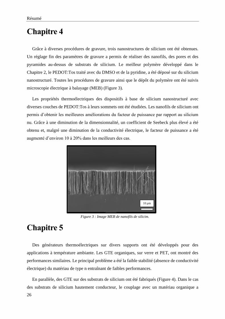
Grâce à diverses procédures de gravure, trois nanostructures de silicium ont été obtenues.
Un réglage fin des paramètres de gravure a permis de réaliser des nanofils, des pores et des
pyramides au-dessus de substrats de silicium. Le meilleur polymère développé dans le
Chapitre 2, le PEDOT:Tos traité avec du DMSO et de la pyridine, a été déposé sur du silicium
nanostructuré. Toutes les procédures de gravure ainsi que le dépôt du polymère ont été suivis
microscopie électrique à balayage (MEB) (Figure 3).
Les propriétés thermoélectriques des dispositifs à base de silicium nanostructuré avec
diverses couches de PEDOT:Tos à leurs sommets ont été étudiées. Les nanofils de silicium ont
permis d’obtenir les meilleures améliorations du facteur de puissance par rapport au silicium
nu. Grâce à une diminution de la dimensionnalité, un coefficient de Seebeck plus élevé a été
obtenu et, malgré une diminution de la conductivité électrique, le facteur de puissance a été
augmenté d’environ 10 à 20% dans les meilleurs des cas.
Chapitre 5
Des générateurs thermoélectriques sur divers supports ont été développés pour des
applications à température ambiante. Les GTE organiques, sur verre et PET, ont montré des
performances similaires. Le principal problème a été la faible stabilité (absence de conductivité
électrique) du matériau de type n entraînant de faibles performances.
En parallèle, des GTE sur des substrats de silicium ont été fabriqués (Figure 4). Dans le cas
des substrats de silicium hautement conducteur, le couplage avec un matériau organique a
10 µm
Figure 3 : Image MEB de nanofils de silicim.

Résumé
27
permis d’obtenir une amélioration des performances du dispositif. En nanostructurant la surface
du silicium, de meilleures performances ont été obtenues pour les générateurs
thermoélectriques hybrides PEDOT:Tos-silicium. Cette amélioration pourrait être expliquée en
partie par un transfert de charge à l'interface silicium-organique, ce qui a permis d'atteindre une
puissance record de 2350 nW pour un générateur à trois jambes à base de PEDOT:Tos sur
silicium nanostructuré sous un ΔT = 10 °C près de la température ambiante.
Malheureusement, cette amélioration n’a pas pu être vérifiée, même avec des techniques
analytiques poussées. Ces résultats sont en accord avec les études récentes sur les systèmes
hybrides. Les scientifiques se sont concentrés sur l'utilisation de diverses stratégies (transport
interfacial et effets structurels/morphologiques) pour améliorer les performances
thermoélectriques. Cependant, il s'est avéré difficile d'établir la physique fondamentale à
l'origine de ces améliorations de performance. La mise au point de matériaux et d'un dispositif
hybrides thermoélectriques de nouvelle génération nécessite une meilleure compréhension de
la physique du transporteur dans les systèmes multiphases complexes.
Conclusion
La thermoélectricité organique et hybride est un domaine qui est encore à ses balbutiements
et présente de nombreuses possibilités d’exploration. L'émergence récente des technologies de
communication, ainsi que les problèmes d'énergie et la menace du réchauffement climatique,
pourraient faire des dispositifs thermoélectriques organiques et hybrides un marché important.
Pour que les produits thermoélectriques trouvent leur place dans ce contexte de nouvelles
technologies émergentes, il est encore nécessaire de surmonter les obstacles liés aux
performances et aux processus de fabrication des dispositifs thermoélectriques.
Figure 4 : Photographie d’un générateur thermoélectrique hybride à base PEDOT:Tos sur substrat de silicium.
Résumé
28
L'objectif principal de ce doctorat, la fabrication d’un générateur thermoélectrique à base de
matériaux organiques a été abordée avec succès. La philosophie de ce travail était d’utiliser les
avantages des matériaux organiques et inorganiques pour atteindre des performances
thermoélectriques élevées.
Ainsi, les polymères de type p synthétisés ont été formulés avec divers agents dopants et
additifs pour optimiser leurs performances thermoélectriques. Quant aux matériaux organiques
de type n, ils ont également été optimisés et caractérisés, malgré leur faible stabilité à l'air. Ainsi
grâce à un réglage fin des propriétés électroniques, les meilleurs matériaux pour les séries de
type p & n ont été le PEDOT: Tos avec un facteur de puissance de 240 µW/mK² et PCBM avec
un facteur de puissance de 2,44 µW/mK.
Tous les matériaux organiques ont été combinés avec des substrats de silicium de type p et
n. Les propriétés thermoélectriques, le coefficient Seebeck, la conductivité électrique et le
facteur de puissance ont été mesurés pour chaque matériau hybride. Les résultats ont montré un
comportement intéressant avec l’augmentation de l'épaisseur de la couche de polymère. En fait,
les propriétés thermoélectriques pourraient être ajustées avec cette stratégie. Bien que l'origine
de ce comportement ne soit pas complètement clarifiée, il pourrait être envisagé comme un
phénomène de transfert de charge à l’interface.
La pénurie de matériaux thermoélectriques de type n (fortement liée à leur instabilité dans
l'air ambiant) a obligé à proposer de nouvelles approches de synthèse de ces matériaux. La
nouvelle approche, avec un substrat en silicium et un matériau organique à la surface, a permis
de développer un matériau de type n stable à l’air efficace pour les applications
thermoélectriques. En fait, les impuretés à l'intérieur du substrat de silicium ont grandement
influencé le type de porteur de charge dans le matériau hybride. Ainsi, avec du silicium dopé
négativement, les dispositifs correspondants étaient de type n (en ce qui concerne son
coefficient de Seebeck), malgré le dépôt de matière organique de type p. Le dispositif hybride
à base de PEDOT: Tos et de silicium de type n a atteint une valeur record de 0,65 mW/mK²,
l’une des meilleures valeurs pour les matériaux hybrides de type n.
Ensuite, la surface de silicium a été nanostructurée, donnant des indications supplémentaires
sur le rôle de l'interface sur les propriétés thermoélectriques. En fait, l’augmentation de la
surface spécifique a produit une amélioration des propriétés thermoélectriques par rapport au
silicium nu. Malgré l'utilisation exclusive de PEDOT:Tos, cette stratégie pourrait être appliquée
à n'importe quel matériau organique et la même amélioration devrait être obtenue.
Résumé
29
Enfin, des générateurs thermoélectriques ont été fabriqués à l'aide de ces systèmes hybrides.
La meilleure puissance de sortie, 2350 nW, a été obtenue pour un TEG à trois jambes constitué
de six couches PEDOT:Tos sur des nanofils de silicium avec une différence de températures de
10°C à température ambiante. Cette étude a été conçue pour aborder différents aspects et
problématiques de la thermoélectricité dans le domaine organique.

30

General Introduction
31
General Introduction
Food and heating are the basic needs of human beings. A long time ago fire allowed human
beings to improve their living conditions [1]. Since then we have sought to diversify our means
of producing thermal energy, and then to diversify the forms of energy. Initially, the main
source of thermal energy was biomass (wood, animal excrement ...) with fire. This has evolved
throughout history with, for example, the use of fossil fuels. The sources then diversified
through discovery and technical progress to be today’s wide energy sources including:
mechanical energy [2] via friction and shocks, nuclear energy [3] via fission, radiant energy [4]
via solar collectors or even geothermal energy [5] can, amongst other things, produce heat. This
multitude of sources allows widespread use of thermal energy and to be relatively well
distributed on Earth.
Nevertheless, the production of heat is not always desired. Much of it is untapped and
released directly into the atmosphere [6]. Every year, the Lawrence Livermore National
Laboratory (founded by UC Berkeley) aim to chart all U.S. energy use in one Sankey diagram
(Figure 1). This diagram includes the original energy source (i.e. nuclear, oil, wind, etc.) as well
as the ultimate end-use (i.e. residential, commercial, etc.) for the energy that was generated (a
single quad is roughly equivalent to 8 billion gallons of gasoline).
One interesting aspect of the diagram is that it also shows rejected energy, which represents
the energy that is wasted due to various inefficiencies. In fact, 68% of all energy generated is
not harnessed for any productive use. This is primarily due to the fact that gasoline engines are
usually only about 20-40% efficient, and even electric engines waste energy since they are
85- 90% efficient. A certain percentage of energy is always released as heat, sound, light, or
other forms that are hard for us to harness.

General Introduction
32
Figure 2 : Sankey diagram of U.S. energy consumption in 2018
This lost energy can be valorised in order to increase the energy yields of the systems. For
example, the heat generated by a process can be recovered and sent to areas that need to be
heated (homes, tertiary sector buildings, ...) [7]. Direct heat recovery for heating is not always
relevant, mainly because the amount of energy and the temperature level are not sufficient. This
problem is accentuated when the zones to be heated are too far from the point of heat
production.
Today, human beings seek mainly to manage energies and their uses in perspectives of
sustainable development. It is in this context that the various directives of the European
Commission can be summarized, which can be summed up by the "20-20-20" objective for
2020 [8]:
o Decrease greenhouse gas (GHG) emissions by 20% from 1990 emissions;
o Reduce energy consumption by 20% through improved energy efficiency;
o Achieve 20% renewable energy in the energy mix.
Recently, on January 22nd, 2014, a new proposal from the European Commission supporting
a reinforcement of this energy-climate policy was published [9]. The goal is to achieve a GHG
reduction of 40% and a 27% renewable energy rate by 2030.

General Introduction
33
Among the various renewable energies, thermoelectricity is the solution for the conversion
of heat losses into electricity, and therefore the improvement of thermal efficiency.
However, as pointed out by Cronin Vining, thermoelectricity will not be the only solution to
the global energy crisis [10]. Indeed, it underlines that in view of the yields, the thermoelectric
devices will be used for personal applications, or at best on the energetic losses of private
vehicles. Thus, the impact on the world energetic crisis would be considerably less.
In this regard, researchers are constantly trying to significantly improve the thermoelectric
device properties. Currently, thermoelectric generators are made from inorganic materials [11].
However, their high performance does not erase their defects, like their low abundance of
inorganic elements in earth’s crust and in oceans. For example, the most used inorganic material
in thermoelectric generators (TEGs), Bismuth Telluride - Bi2Te3, is composed of the Earth’s
two rarest “metals” [12]. Furthermore, weight is also a limitation for embedded applications.
Finally, their low processability, high toxicity and high cost ($806/kg) are problematic for
future device use [13].
Thanks to the discovery of Shirakawa, Mac Diarmid and Heeger in 1977, oxidized
conjugated polymers could behave electrically as a metal [14,15], and used as an innovative and
competing material for TEGs [16]. Conducting polymers have already been used in various fields
such as in the fabrication of flexible organic solar cells [17], flexible organic light emitting [18],
or flexible sensors [19]. In the past 10 years, the thermoelectric properties of conducting
polymers have gained a lot of attention from the scientific community [20]. Indeed, conducting
polymer’s strength lie in their intrinsic low thermal conductivity, a high electrical conductivity
(with a proper structure tuning), a high processability (printable techniques available) and low
cost [21– 25]. However, their low efficiency compare to inorganic TEGs limits their application
to low powered devices. Many efforts are being made to improve their properties.
The aim of this Ph.D. is to develop an efficient thermoelectric generator based on organic
materials. Several optimization routes have been investigated in this work, either by fine-tuning
of the synthetic parameters leading to the thermoelectric material or by associating organic and
inorganic materials in a thermoelectric composite.
In this manuscript, Chapter 1 provides a basic overview of thermoelectricity. Starting with a
brief history of thermoelectricity, as well as the basic theory of these related phenomena, some
highlights from the literature with a focus on state-of-the-art studies in this field will be
General Introduction
34
provided. Chapter 1 summarizes the knowledge and understanding of polymers in the
thermoelectric field, and their use as an innovative material in the thermoelectric generator.
The following Chapters describe the works and studies realized during this Ph. D. Chapter 2
discusses the optimization of polymer and organics materials for thermoelectricity. Most
famous p-type materials, such as PEDOT, P3HT, and PCDTBT were studied. Likewise, n-type
material, PCBM and a new polymer with selenium were used. When these organic materials
were optimized, a novel approach developed in our laboratory was used to enhance
thermoelectric properties. Silicon was used as a substrate to benefit from these properties. The
interface between the organic material and the silicon substrate was the point as a keystone to
achieving enhancement of thermoelectric properties, Chapter 3 and 4 described results
obtained.
The last Chapter 5, describes the fabrication of TEGs based on works previously done in
other Chapters. The production and characterization of various forms of thermoelectric
generators were developed. Finally, at the end of this manuscript, different appendices provide
some insights on the polymer theoretical background, the experimental procedures and other
parallel studies, respectively.

General Introduction
35
References
[1] L. Henry, La domestication du feu aux temps paléolithiques ; Odile Jacob : Paris, 2017.
[2] P. Breeze, Power Generation Technologies; Elsevier, 2014.
[3] K. Saidi and M. B. Mbarek, Progress in Nuclear Energy, 2016, 88, 364-374.
[4] G. L. Smith, K. J. Priestley, N. G. Loeb, B. A. Wielicki, T. P. Charlock, P. Minnis, D.
R. Doelling, D. A. Rutan, Adv. Space Res. 2011, 48, 254.
[5] J. Zhu, K. Hu, X. Lu, X. Huang, K. Liu, X. Wu, Energy 2015, 93, 466.
[6] H. Harde, Int. J. Atmospheric Sci. 2013, Article ID 503727, pp26.
[7] H. Jouhara, N. Khordehgah, S. Almahmoud, B. Delpech, A. Chauhan, S. A. Tassou,
Therm. Sci. Eng. Prog. 2018, 6, 268.
[8] European Commission, 2020 climate & energy package. Clim. Action - Eur. Comm.
2016.
[9] European Commission, 2030 climate & energy framework. Clim. Action - Eur. Comm.
2016.
[10] C. B. Vining, Nat. Mater. 2009, 8, 83.
[11] M.-K. Han, Y. Jin, D.-H. Lee, S.-J. Kim, Materials 2017, 10, 1235.
[12] O. Eibl, K. Nielsch, N. Peranio, F. Völklein, Thermoelectric Bi2Te3 Nanomaterials;
John Wiley & Sons, 2015.
[13] N. Lowhorn, W. K. Wong-Ng, J. Lu, E. L. Thomas, M. Otani, M. L. Green, N. Dilley,
J. Sharp, T. N. Tran, Appl. Phys. -Mater. Sci. Process. 2009, 96.
[14] A. J. Heeger, Rev. Mod. Phys. 2001, 73, 681.
[15] M. Geoghegan, G. Hadziioannou, Polymer Electronics; Oxford Master Series in
Physics; Oxford University Press: Oxford, New York, 2013.
[16] B. Russ, A. Glaudell, J. J. Urban, M. L. Chabinyc, R. A. Segalman, Nat. Rev. Mater.
2016, 1, 16050.
[17] A. I. Hofmann, W. T. T. Smaal, M. Mumtaz, D. Katsigiannopoulos, C. Brochon, F.
Schütze, O. R. Hild, E. Cloutet, G. Hadziioannou, Angew. Chem. Int. Ed. 2015, 54,
8506.
[18] M. Kuik, G.-J. A. H. Wetzelaer, H. T. Nicolai, N. I. Craciun, D. M. D. Leeuw, P. W.
M. Blom, Adv. Mater. 2014, 26, 512.
[19] K. M. Persson, R. Gabrielsson, A. Sawatdee, D. Nilsson, P. Konradsson, M. Berggren,
Langmuir 2014, 30, 6257.
[20] O. Bubnova, X. Crispin, Energy Environ. Sci. 2012, 5, 9345.
[21] X.-S. Wang, H.-P. Tang, X.-D. Li, X. Hua, Int. J. Mol. Sci. 2009, 10, 5257.
[22] T.-H. Le, Y. Kim, H. Yoon, Polymers 2017, 9, 150.
[23] M. Aldissi, Mol. Cryst. Liq. Cryst. Inc. Nonlinear Opt. 1988, 160, 121.
[24] C. Huang, X. Qian, R. Yang, Mater. Sci. Eng. R Rep. 2018, 132, 1.
[25] T. O. Magu, A. U. Agobi, L. Hitler, P. M. Dass, J. Chem. Rev. 2019, 1, 19.

36

Chapter 1 Thermoelectric state of the art
37
Chapter 1
Thermoelectricity state of the art:
From origin to recent device

Chapter 1 Thermoelectric state of the art
38
A Fundamentals of thermoelectric materials
Historic
Thermoelectricity began in 1794 with Alessandro Volta, when he highlighted the appearance
of a "force" under a temperature gradient thanks to glasses of water with iron and frog parts
(Figure 1) [1].
Figure 1: Volta’s experiment. A – Metal bow (iron), B – Glass full of water, C & D Frog parts immerged in
glasses.
It will take three decades for the interest of scientists for thermoelectricity to come back. In
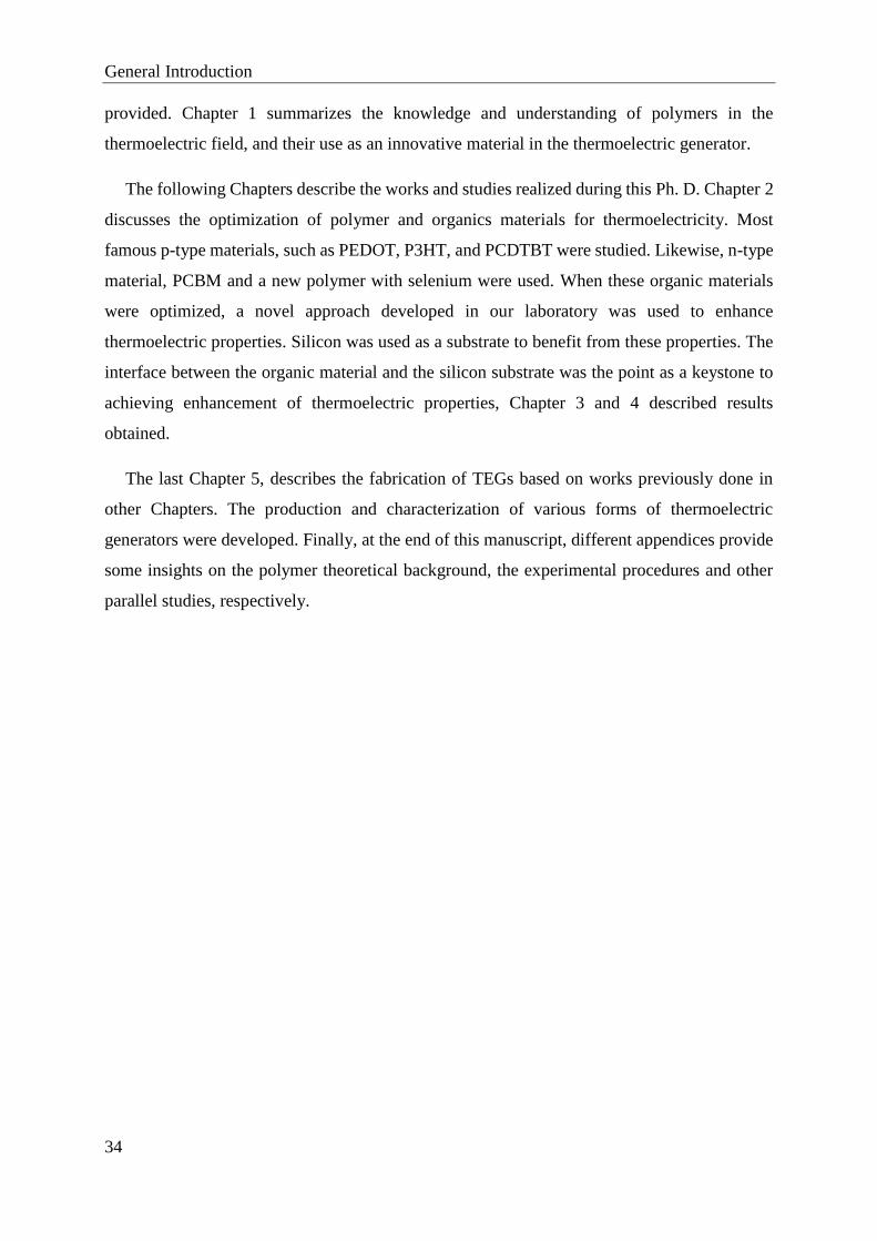
1821, Thomas Johann Seebeck shown that when a temperature gradient is applied to a circuit
built with two metallic conductors and a needle, the latter is deviated (Figure 2) [2]. Seebeck
mistakenly thinks that this effect is due to the magnetic field induced by the difference in
temperature and that it must be connected to the Earth's magnetic field. At the same time, Hans
Christian Oersted and Gustav Magnus tried to explain this phenomenon. First, Hans Christian
Oersted explained that the temperature gradient creates a potential difference so if the circuit is
closed and allows current flow, a magnetic field is induced [3]. Then Gustav Magnus discovered
the Seebeck voltage was independent on thermal distribution along the material junction, the
thermopower was a thermodynamic state function [4].
Chapter 1 Thermoelectric state of the art
39
Figure 2: Thomas Johann Seebeck first experiment
Few years after these discoveries, in 1834, Jean Peltier, realized that an electrical current
flow could produce or absorb heat at the junction of two metallic materials [5]. This phenomenon
was explained later by Emil Lenz, he put ice around a bismuth-antimony junction, and by
reversing electrical current flow, he melted the ice. So heating or cooling was dependent of
current direction flow [6]. Later, in 1840's, James Prescott Joule demonstrated an irreversible
phenomenon, when an electric current flowed in a material because of the internal resistance of
the material, heat is produced. This heat's quantity is related to the square of current intensity
and the internal resistance, it's called Joule effect [7].
It took twenty years, thanks to William Thomson (Lord Kelvin), to link Seebeck and Peltier
effects (Appendix I) with Kelvin equations. He also predicted a third phenomenon, called
Thomson effect (Appendix I). When a temperature gradient and an electrical current flow are
present simultaneously, heat emission or absorption could happen in material [8].
Volta, Seebeck, Peltier and Thomson (Lord Kelvin) are the pioneers in the field of
thermoelectricity. Their understanding of different phenomena has greatly contributed to the
current advances. However, due to the complexity of this phenomena, it's only in the next
century that for the first time an efficiency for a thermoelectric generator is calculated based on
Seebeck coefficient thanks to Edmund Altenkirch [9]. Later, he extended his calculation on
cooling and described optimal operating conditions for this devices.
Thermoelectric effects
This section introduces the fundamentals of thermoelectric effects, mainly focused on
Seebeck coefficient and electrical and thermal conductivity (i.e Figure of merit ZT), by a general
approach of their physics and in particular a focus on semiconductors material.

Chapter 1 Thermoelectric state of the art
40
Thermoelectricity combines two phenomena, the heat flux (“thermos”) and the electric
current (“electricity”) for a same material. Thermoelectric system can either harvest waste heat
to convert it in electricity or convert an applied voltage into a cooling or heating source. The
first effect, a temperature gradient results in the production of a voltage, is called Seebeck
coefficient (S). The other effect, opposed to Seebeck coefficient, the Peltier effect (Π) described
the presence of heating or cooling at the electrified junction of two conductors.
So thermoelectric effects link the fluxes between the current density 𝐽𝑒 , and heat carriers 𝐽𝑞 .
In order to explain this relation, electric current density equation (Ohm’s law) and heat
conduction (Fourrier’s Law) have to be considered [4–8].
Ohm’s law expresses current density 𝐽𝑒 through material and can be related to electrical
conductivity σ to a specific electric field :
𝐽𝑒 = σ E (1)
When a temperature gradient T is applied in the material, equation (1) becomes:
𝐽𝑒 = σ E − 𝜎𝑆 𝑇 (2)
Current density is expressed with two terms, one related to the electrical field and another
related to the temperature gradient that will induce an internal carrier diffusion. In the last term,
the Seebeck coefficient S appear and is expressed in volts per Kelvin (V/K). This parameter is
one of the most important parameter in thermoelectricity.
2.1 Seebeck effect
The Seebeck effect gains great interest in semiconductors field, as it allows for determination
of the type of the dominating charge carriers in a material as well as the relative position of the
Fermi level with respect to the transport level.

Chapter 1 Thermoelectric state of the art
41
Practically, when a temperature difference ∆T is applied on a material, a potential difference
ΔV is generated, which is proportional to this temperature difference ∆T. The proportionality is
given by an intrinsic material property called Seebeck coefficient S.
S = −∆𝑉
∆𝑇 (3)
Seebeck coefficient could be understood as follows: In a semiconductor, the energetic
distribution of free charge carriers is shifted to higher energy states upon heating. So, if one
side of the material is hotter than the other, the charge carriers on the hotter side have higher
energies. This leads to a displacement diffusion current towards cold side, resulting in a
charging of the two sides of the material. With increasing charge accumulation at the sides, an
electric field opposite to the diffusion current builds up, limiting the total voltage being
generated (Figure 3). If electrons are the dominating charge carriers, the cold side will be
charged negatively, whereas for hole dominated materials the cold side is charged positively.
Figure 3: Sketch illustrating the thermoelectric effect.
(a) n-type material (electrons) & (b) p-type (holes) material under a temperature gradient
Seebeck coefficient could be also explained by energy band diagram. In Figure 4, an
idealized n-type semi-conducting material is sandwiched between two metallic electrodes
(contacts are considered perfect) [10]. However, an energy barrier ΦCN at the interface is present,
it’s simply a difference between barrier energy of conduction band EC and Fermi level EF.

Chapter 1 Thermoelectric state of the art
42
Without temperature gradient (Figure 4 (a)), Fermi levels are aligned and no open-circuit
voltage is present (Voc = 0). On the other side, when temperature of metallic contact 2 increases
(T2 > T1), Fermi level on the same side will decrease towards Fermi level of the intrinsic
semi-conducting material (Figure 4 (b)). So electrons will cross more easily the energetic barrier
of the hot side. Because density of states appears at higher energy level than EC; average energy,
where electrons are localized, will be called Δx (Figure 4 (b)).
So temperature gradient generates a positive voltage on hot contact 2, creating a potential
difference ΔV following Fermi level difference between hot and cold contact:
EF2 = EF1 −𝑞𝛥𝑉 (4)
In an open-circuit, electrical current J is zero, so electrons can’t move. Generated voltage
adjusts to temperature difference to balance energy’s system and stop electron movement. Thus,
if J =0, the probability f1 to have an electron hoping form cold contact to EC +Δx is equal to the
probability f2 to have an electron hoping from hot contact to EC +Δx. This could be translated
by the following equation:
f1 = f2 → f1 [𝐸𝑐(0) + ∆𝑥] = f2 [𝐸𝑐(0) + ∆𝑥] (5)
Figure 4: Analysis of Seebeck effect with energy band diagrams.
(a) Without temperature gradient. (b) With a temperature gradient.

Chapter 1 Thermoelectric state of the art
43
By applying Fermi-Dirac distribution on f1 and f2, the equation becomes:
1
1+ⅇ(𝐸𝑐+𝛥𝑥−𝐸𝐹1)/𝑘𝐵𝑇1 =
1
1+ⅇ(𝐸𝑐+𝛥𝑥−𝐸𝐹2)/𝑘𝐵𝑇2 (6)
Which leads to:
(𝐸𝑐 + 𝛥𝑥 − 𝐸𝐹1)/𝑘𝐵𝑇1 = (𝐸𝑐 + 𝛥𝑥 − 𝐸𝐹1 + 𝑞𝛥𝑉)/𝑘𝐵𝑇2 (7)
The equation can be express as:
∆V = −(𝐸𝑐 + 𝛥𝑥 − 𝐸𝐹1)
q𝑇1 𝛥𝑇 (8)
Finally, Seebeck coefficient appears in the equation with S = ΔV / ΔT and can be written as:
S = −𝐸𝑐 − 𝐸𝐹1
q𝑇1−
𝛥𝑥
q𝑇1= −(
𝑘𝐵
𝑞) (
𝐸𝑐 − 𝐸𝐹1
𝑘𝐵𝑇1+
𝛥𝑥
𝑘𝐵𝑇1) (9)
S = (𝑘𝐵
𝑞) (
𝐸𝐹1 − 𝐸𝑉
𝑘𝐵𝑇1−
𝛥𝑥
𝑘𝐵𝑇1) (10)
By convention for semi-conductors, Seebeck coefficient is negative for n-type and positive
for p-type materials. Thanks to equation above, Seebeck coefficient is proportional to the
energy difference between band energy ((EC + Δx) or (EV - Δx)) and Fermi level energy. It means,
in case of highly degenerated materials, like metals or highly doped semi-conductors, Fermi
level is near EC (or EV) and so Seebeck coefficient tend to zero. Thus, semi-conducting materials
will have high Seebeck coefficient.
Chapter 1 Thermoelectric state of the art
44
2.2 Electrical conductivity
Electrical conductivity σ is also an important parameter in thermoelectric field. This is
material inherent property to conduct current, and is linked to charge carrier transport [11]. Based
on equation (1), electrical conductivity can be expressed as:
𝜎 =J
E (11)
In a homogenous material, current density J is equal to conduction current Jd.
In semi- conductors, current density is given by the following relation:
𝐽𝑑 = 𝐽𝑑𝑛 + 𝐽𝑑𝑝 = 𝑞(µ𝑛𝑛 + µ𝑝𝑝)𝐸 (12)
Where µn and µp are electrons and holes mobility, n & p are charge carrier concentration of
electrons and holes, and q is elementary charge. Thanks to the previous equations, electrical
conductivity is:
𝜎 = 𝑞(µ𝑛𝑛 + µ𝑝𝑝) (13)
Electrical conductivity thought electrical mobility is an important parameter for charge
carrier transport characterization and devices performances.
2.3 Thermal conductivity
The last important parameter that is involved in thermoelectricity is the thermal conductivity
[11]. Thermal conductivity κ is a thermal conduction without matter displacement that can be
defined as a ratio between heat flux density 𝐽𝑞 and temperature gradient 𝑇 based on Fourier’s
law:

Chapter 1 Thermoelectric state of the art
45
κ = −𝐽𝑞
𝑇 (14)
So dependence of thermal flux to temperature gradient shows that thermal energy transfer is
a random process based on diffusivity and particles collision inside the material. In case of
metals and heavily doped inorganic semi-conductors, κ is separated into two contributions, the
structural, κs, and the electronic contribution, κe, as the charge carriers of the material also
contribute to the propagation of the phonons in the material [6,7]. For metals the electronic
contribution is dominant in the thermal conductivity and is based on the fact that the charge
carriers are involved in both the heat and charge transport in the material [8]. So thermal
conductivity is expressed as:
κe = 𝜎𝐿𝑇 (15)
where L is Lorentz number depending on band structure, diffusivity and level of
degeneration. For metals the Lorenz number is equal to the Sommerfield value, and it is
commonly used to calculate the thermal conductivity from the electrical conductivity in
metals [7]. However, for inorganic semiconductors, the Lorenz number deviates from the
Sommerfield value, due to the introduction of disorder into the system [7].
2.4 Figure of Merit ZT
Thanks to Edmund Altenkirch in 1911 who introduced the concept of dimensionless unit
(Figure of merit, ZT), thermoelectric materials performance can be evaluated [12]. Then Abram
Fedorovich Ioffe, in 1931, applied successfully this concept to semiconductors materials [13].
Because only material properties are involved in ZT expression; the figure of merit express
material efficiency in heat-electricity conversion. ZT is the reference in the classification of
thermoelectric materials. The figure of merit is defined by following equation:

Chapter 1 Thermoelectric state of the art
46
𝑍𝑇 = 𝑆²𝜎
𝜅 𝑇 (16)
Where the electrical conductivity σ, Seebeck coefficient S, thermal conductivity κ of the
material and the operating temperature T (average temperature between the hot and cold sides)
are expressed [14]. The product in the numerator, S²σ, is known as the Power Factor (PF).
Sometimes PF is used to compare thermoelectric materials when κ is ignored because of its
weak evolution or difficulty to be measured.
Improving thermoelectric performance is fundamentally challenging because S and σ are
anti-correlated, and coupled with κ. The enhancement challenge is graphically illustrated in
Figure 5. The ZT relationship suggests that to improve performance one might aim to enhance
the electrical conductivity, which can be done, for example, by increasing the carrier
concentration, n (𝜎=𝑛𝑞𝜇). However, increasing the carrier concentration generally leads to a
reduction in the material’s Seebeck coefficient and an increase in the thermal conductivity. As
a result, improvements in ZT have been hard to achieve and limited to an optimization problem.
Useful thermoelectric materials are typically doped semiconductors or semi-metals that can
balance the thermal and electrical properties [14–18]. The ideal thermoelectric material, therefore
has very low κ and high 𝜎, which is often described as a “phonon-glass, electron-crystal” [18].
Figure 5: Seebeck coefficient, electrical conductivity, thermal conductivity and ZT as function of free carrier
concentration [15 - 17].

Chapter 1 Thermoelectric state of the art
47
The best thermoelectric material in 2016, with high ZT, were bismuth telluride alloys at low
temperature (ZT = 1.86 at 320K) and lead telluride at high temperature (ZT = 2.2 at 915K) [19].
Thermoelectric device
A thermoelectric device is composed of two thermoelectric materials, a n-type (electron
transporting) and a p-type (hole transporting) semiconductor, connected together electrically in
series and thermally in parallel. One n-type or p-type part is called “leg” or “plug”. The array
is sandwiched between electrically insulating heat spreaders on both the hot side and cold side.
Under an applied thermal gradient, charge carriers flow from the hot to the cold side, and the
resulting electrical potential can be harnessed as usable electricity (Figure 6 (a)). If operated in
reverse (flowing electricity through the material to generate a temperature difference),
thermoelectric effects can also be used for cooling applications as Peltier coolers (Figure 6 (b)).
This part is focused on power generation device. Device thermoelectric efficiency ηTE is
defined by the ratio between electric power produced Pe on thermic flux crossing hot side Qc
[14,20]. The equation is given below (equation (17)) and some hypothesis were made (more
details about this equation (17) in Chapter 5):
o Material thermoelectric properties are constant;
o Temperature on each side is uniform;
o All heat flux crosses thermoelectric materials from hot side to cold side;
o Electric contact between thermoelectric materials are supposed perfect.
Figure 6: Schematic principle of (a) Seebeck and (b) Peltier effects under a gradient of temperature

Chapter 1 Thermoelectric state of the art
48
𝜂𝑇𝐸 =
𝑃𝑒
𝑄𝑐=
𝑇𝐻− 𝑇𝐶
𝑇𝐻 .
𝑚𝑚 + 1
1 + (𝑚 + 1)𝑍 . 𝑇𝐶
−
𝑇𝐶
𝑇𝐻
2 . 𝑇𝐶 . (𝑚 + 1)
(17)
Where TH is the temperature at the hot junction, TC is the temperature at the cold junction
and m is the ratio between load electric resistance on internal electric resistance of the
thermoelectric module. By using an optimal value for m (mopt = √1 + 𝑍𝑇 ), shown by Ioffe [21],
device thermoelectric efficiency ηTE becomes maximal efficiency ηmax [22]:
𝜂𝑇𝐸 𝑚𝑎𝑥 =𝑃𝑒
𝑄𝑐=
𝑇𝐻− 𝑇𝐶
𝑇𝐻 .
√1 + 𝑍𝑇 − 1
√1 + 𝑍𝑇 + 1 (18)
In these equations, the term 𝑇𝐻− 𝑇𝐶
𝑇𝐻 is related to Carnot cycle efficiency for reversible process.
The second term is directly related to thermoelectric system (ZT) and has an huge influence on
thermoelectric efficiency 𝜂𝑇𝐸 value as this shown Figure 7. But, because thermoelectric cycle
isn’t a reversible process, that means conversion efficiency can’t achieve maximum Carnot
efficiency. This limitation is due to all irreversible process from ZT parameters.
Figure 7: Thermoelectric efficiency as function of temperature for different ZT value

Chapter 1 Thermoelectric state of the art
49
So performing thermoelectric material must have high ZT value in order to obtain the best
efficiency. Thanks to Figure 5, an overview of changes in physical characteristics as a function
of charge concentration is possible. Thus there exists an optimal charge density at the
maximization of ZT, and that corresponds to the field of semiconductors. For high temperature
applications, such as waste heat recovery from vehicle exhaust, only inorganic materials are
stable enough to be useful and active research is ongoing into a number of inorganic classes of
materials, including silicides, skutterudites, half Heusler alloys, inorganic clathrates, and oxides
[18]. At low operating temperatures (below 200°C), alloys of the inorganic semiconductor,
bismuth telluride (Bi2Te3), have long been the benchmark thermoelectric material with a ZT of
approximately 1 (which equates to ~5% efficiency at 100 K temperature difference) [18,23,24]. In
laboratory, a ZT higher than 2 was already obtained, but there are still a number of years before
this type of material will be available for the industry [25]. However, bismuth telluride is toxic,
not earth abundant, and fragile, resulting in rigid and brittle module architectures. Conducting
polymers and molecular semiconductors are an attractive earth abundant alternative for low
temperature applications.
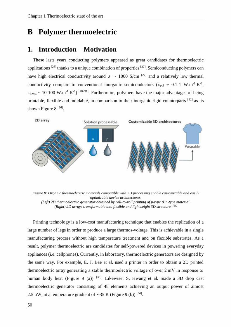
Chapter 1 Thermoelectric state of the art
50
B Polymer thermoelectric
Introduction – Motivation
These lasts years conducting polymers appeared as great candidates for thermoelectric
applications [26] thanks to a unique combination of properties [27]. Semiconducting polymers can
have high electrical conductivity around σ ~ 1000 S/cm [27] and a relatively low thermal
conductivity compare to conventional inorganic semiconductors (κpol ~ 0.1-1 W.m-1.K-1,
κinorg ~ 10-100 W.m-1.K-1) [28–31]. Furthermore, polymers have the major advantages of being
printable, flexible and moldable, in comparison to their inorganic rigid counterparts [32] as its
shown Figure 8 [26].
Printing technology is a low-cost manufacturing technique that enables the replication of a
large number of legs in order to produce a large thermos-voltage. This is achievable in a single
manufacturing process without high temperature treatment and on flexible substrates. As a
result, polymer thermoelectric are candidates for self-powered devices in powering everyday
appliances (i.e. cellphones). Currently, in laboratory, thermoelectric generators are designed by
the same way. For example, E. J. Bae et al. used a printer in order to obtain a 2D printed
thermoelectric array generating a stable thermoelectric voltage of over 2 mV in response to
human body heat (Figure 9 (a)) [33]. Likewise, S. Hwang et al. made a 3D drop cast
thermoelectric generator consisting of 48 elements achieving an output power of almost
2.5 μW, at a temperature gradient of ∼35 K (Figure 9 (b)) [34].
Figure 8: Organic thermoelectric materials compatible with 2D processing enable customizable and easily
optimizable device architectures.
(Left) 2D thermoelectric generator obtained by roll-to-roll printing of p-type & n-type material.
(Right) 2D arrays transformable into flexible and lightweight 3D structure. [26]

Chapter 1 Thermoelectric state of the art
51
Promising results were obtained thanks to rigorous strategic material design, in order to
compete with efficiencies of inorganic thermoelectric generator. However, the main
disadvantage of polymers is their lower thermoelectric efficiency in comparison to their
inorganic compartments. In the next parts, several reported strategies on the enhancement of
the thermoelectric properties of polymers (p- & n-type) are going to be reviewed.
p-Type thermoelectric material
At their beginning, conducting polymers were not envisioned as prospective thermoelectric
materials. The first conducting organic polymer to be extensively studied was
trans-polyacetylene [35–39]. Conductivities of 560 S.cm−1 and high carrier mobilities of
approximately 1 cm2.V−1.s−1, due to polyacetylene linearity, were reported when p-doped with
arsenic pentafluoride (AsF5). The first Seebeck measurement was done on this polyacetylene
to understand the nature of the charge carrier. By varying the doping level of polyacetylene,
Park et al., shown that the Seebeck coefficient decreases for high carrier concentrations [40].
Nevertheless, it’s only thirty years later that Hiroshige et al. reported the first demonstration of
the potential for polymers in thermoelectric (ZT = 0,1) by doping PPV with iodine [41].
The representative p-type thermoelectric polymer include poly(3,4-ethylenedioxythiopene)
(PEDOT), polythiophene derivatives (more particularly poly(3-hexylthiophene, P3HT),
polyaniline (PANi), polypyrrole, polyphenylenevinylene (PPV), polycarbazole (like poly[N-
9'-heptadecanyl-2,7-carbazole-alt-5,5-(4,7-di-2-thienyl-2',1',3'-benzothiadiazole], PCDTBT)
and poly(benzodithiophene) (like Poly[[4,8-bis[(2-ethylhexyl)oxy]benzo[1,2-b:4,5-
b']dithiophene-2,6-diyl][3-fluoro-2-[(2-ethylhexyl) carbonyl] thieno[3,4-b]thiophenediyl]],
PTB7) (Figure 10).
(a) (b)
Figure 9: (a) Image of a 32-legs planar thermoelectric generator on flexible PET substrate [33].
(b) Image of a 48 elements 3D thermoelectric generator on flexible PET substrate [34].
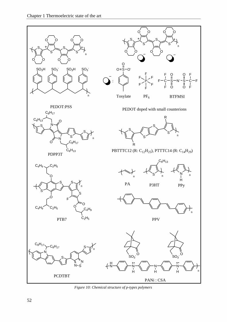
Chapter 1 Thermoelectric state of the art
52
S
O O
S
OO
S
O O
S
OO
n
SO3H SO3- SO3H SO3
-
n
S
O O
S
OO
S
O O
S
OO
n
:
n
S
C6H13
nN n
H
S
S
O
O
S
S
F
OOC2H5C4H9 C4H9
C2H5
C4H9 C2H5
n
N
C8H17 C8H17
S
N S
N
Sn
S O-O
O
P-FF
F
F
FFS N- S
O
O
C
F
F
F
O
O
C
F
F
F
S
S
S
S
R
R
n
n
NHN N N
H H H
SO3- O
SO3- O
n
PEDOT:PSS
Tosylate PF6 BTFMSI
PEDOT doped with small counterions
PBTTTC12 (R: C12H25), PTTTC14 (R: C14H29)
PTB7
PCDTBTPANi : CSA
PA PPy
PPV
P3HT
S N
N
C8H17
C6H13 O
O C8H17
C6H13
S
S
PDPP3T
n
Figure 10: Chemical structure of p-types polymers
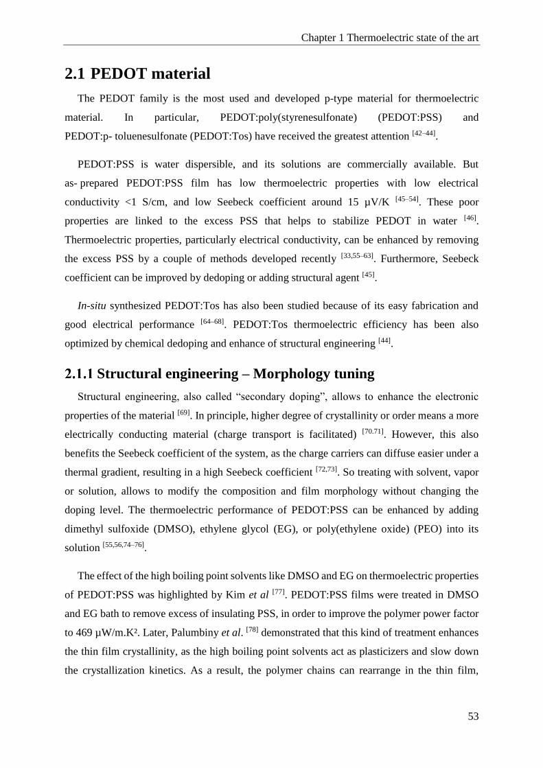
Chapter 1 Thermoelectric state of the art
53
2.1 PEDOT material
The PEDOT family is the most used and developed p-type material for thermoelectric
material. In particular, PEDOT:poly(styrenesulfonate) (PEDOT:PSS) and
PEDOT:p- toluenesulfonate (PEDOT:Tos) have received the greatest attention [42–44].
PEDOT:PSS is water dispersible, and its solutions are commercially available. But
as- prepared PEDOT:PSS film has low thermoelectric properties with low electrical
conductivity <1 S/cm, and low Seebeck coefficient around 15 µV/K [45–54]. These poor
properties are linked to the excess PSS that helps to stabilize PEDOT in water [46].
Thermoelectric properties, particularly electrical conductivity, can be enhanced by removing
the excess PSS by a couple of methods developed recently [33,55–63]. Furthermore, Seebeck
coefficient can be improved by dedoping or adding structural agent [45].
In-situ synthesized PEDOT:Tos has also been studied because of its easy fabrication and
good electrical performance [64–68]. PEDOT:Tos thermoelectric efficiency has been also
optimized by chemical dedoping and enhance of structural engineering [44].
Structural engineering – Morphology tuning
Structural engineering, also called “secondary doping”, allows to enhance the electronic
properties of the material [69]. In principle, higher degree of crystallinity or order means a more
electrically conducting material (charge transport is facilitated) [70.71]. However, this also
benefits the Seebeck coefficient of the system, as the charge carriers can diffuse easier under a
thermal gradient, resulting in a high Seebeck coefficient [72,73]. So treating with solvent, vapor
or solution, allows to modify the composition and film morphology without changing the
doping level. The thermoelectric performance of PEDOT:PSS can be enhanced by adding
dimethyl sulfoxide (DMSO), ethylene glycol (EG), or poly(ethylene oxide) (PEO) into its
solution [55,56,74–76].
The effect of the high boiling point solvents like DMSO and EG on thermoelectric properties
of PEDOT:PSS was highlighted by Kim et al [77]. PEDOT:PSS films were treated in DMSO
and EG bath to remove excess of insulating PSS, in order to improve the polymer power factor
to 469 µW/m.K². Later, Palumbiny et al. [78] demonstrated that this kind of treatment enhances
the thin film crystallinity, as the high boiling point solvents act as plasticizers and slow down
the crystallization kinetics. As a result, the polymer chains can rearrange in the thin film,
Chapter 1 Thermoelectric state of the art
54
increasing the degree of crystallinity and assisting the charge carrier transport in the system
(Figure 11) [51,78,79].
More explanation was given by Bubnova et al. [72] proposing that PEDOT derivatives with
increased crystallinity could behave as semimetals, thus having both a high electrical
conductivity and a high Seebeck coefficient. In PEDOT systems of high crystallinity, the
π- orbitals of the PEDOT units recombine into a bipolaron network, which broadens all the
π- orbitals of the polymer, thus increasing the slope at the density of states and the Seebeck
coefficient. As a result, vapor phase polymerized PEDOT:Tos films exhibit power factor as
high as 454 μW/m·K2. In recent years, more studies support the beneficial effect of crystallinity
on the thermoelectric properties of PEDOT derivatives [72,80–82].
Figure 11: Plasticizing effect agents on the PEDOT:PSS structure. When EG is added to PEDOT:PSS material
(b), the crystallization process is shown down resulting in better stacked chains, in comparison to the pure
material (a). When the thin films are further treated with an EG bath, the system recrystallize and shift from a
face-one to an edge-on configuration (c). [57] [78] [79]

Chapter 1 Thermoelectric state of the art
55
In their works, Petsagkourakis et al. correlated charge carrier mobility, thin film crystallinity
and thermoelectric properties of conducting polymers, PEDOT:Tos thin films [73]. Two
additives, DMSO, a high boiling point solvent, and pyridine, an organic base were mixed to the
polymer solution to enhance the degree of crystallinity of PEDOT:Tos thin films
(Figure 12 (b)). This treatment didn’t affect the oxidation level of the polymers, as proven by
X-Ray photoelectron spectroscopy (XPS) (Figure 12 (a)). So the conductivity of these samples
is directly related to the mobility, because the oxidation level is the same. A relationship
between Seebeck coefficient and charge carrier mobility was extracted for those films, S~μ0.2
(Figure 12 (c)).
Tuning of the doping level
One of the biggest concerns about thermoelectric development is the modest electrical
conductivity of intrinsic polymer materials (pristine PEDOT:PSS σ = 0.1 – 0.5 S/cm) [83]. In
case of PEDOT, it was shown that the thermoelectric properties of films could be enhanced by
(a) (b)
(c)
Figure 12: (a) The radially averaged intensity versus the scattering vector q for the various PEDOT :Tos
samples. A higher intensity in the peak corresponding to the (100) reflection is respective to a system of higher
degree of crystallinity. (b) XPS spectra of PEDOT:Tos samples with various solvent additives. (c) Extracted
relationship between Seebeck coefficicent and charge carrier mobility with constant oxidation levels. [73]

Chapter 1 Thermoelectric state of the art
56
removing the unionized portion of the counter-anion molecules, which reduces charge-carrier
mobility [84]. This process is called “de-doping”.
As reference study, Bubnova et al. optimized thermoelectric properties of PEDOT:Tos by
an exposure to reductive vapors. By de-doping the material, the Seebeck coefficient increased
while the electrical conductivity decreased, showing a similar behavior as inorganic materials
(Figure 13). The power factor was optimized from 38 to 324 µW/m.K², and a figure of merit of
0.25 at room temperature was obtained (thermal conductivity of 0.25 W/m.K²) [44].
The degree of de-doping in a material is heavily affected by the electrochemical potential
and the chemical nature of the reducing agent itself as shown by Massonnet et al. [85] upon
dipping films of PEDOT:PSS in different reducing agents like
tetrakis(dimethylamino)ethylene) (TDAE) or hydrazine. Khan et al. [86] shown the impact of
the pH on thermoelectric properties of PEDOT films (Figure 14). The pH of the solutions
impacted the electrical conductivity and the Seebeck coefficient, allowing for optimization of
the system. Later, Fan et al. [87] washed pristine PEDOT:PSS with sulfuric acid then a reducing
agent. The sulfuric acid increases the electrical conductivity both by oxidation and by changing
morphology. The power factor of PEDOT:PSS was enhance from 0.0045 µW/m.K2 to
334 µW/m.K2.
Figure 13: Electrical conductivity σ, Seebeck coefficient S, and the power factor σS², versus the oxidation levels
of the PEDOT:Tos films [44].

Chapter 1 Thermoelectric state of the art
57
Figure 14:UV-Vis spectra of acid and base treated PEDOT:Tos with respect the pH of the treating solution [41]
All previous works concerned conventional chemical redox reaction, an alternative approach
for doping optimization is electrochemical methods, offering a better control. A typical
electrochemical setup is composed of three electrodes: a working, a reference and a counter
electrode. This technique consists in depositing a polymer film by oxidation (anodic
polymerization) on the surface of a noble metal electrode (gold, platinum) [88]. The films
obtained by electrochemical polymerization are films whose properties and structure are better
defined and controlled. Parameters such as temperature, current density, frequency, electrolyte,
counter-ions for PEDOT could be used to modify the morphology and film properties [89].
Park et al. [90] synthesized PEDOT:Tos by this process, and obtained a record power factor of
1270 µW/m.K2. Another use was reported by Bubnova et al. [91] where an organic
electrochemical transistor was used to optimize their thermoelectric properties of PEDOT:PSS.
2.2 Other p-type polymers
Historically, the first conductive polymer was trans-polyacetylene [35–39], a “non-PEDOT
family” p-type polymer. Despite, PEDOT:PSS and derivatives are widely represented in
thermoelectric field, a lot of groups worked on other p-type polymers to obtain the best
thermoelectric generator. As in case of PEDOT, works have been carried out to improve the
thermoelectric properties of p-type polymers through an optimization of their morphology and
level of doping.

Chapter 1 Thermoelectric state of the art
58
Polyacetylene (PA)
When polyacetylene is doped with halogens such as chlorine, bromine or iodine vapors and
with pentafluoride (AsF5) the electrical conductivity could be further increase to 20.000 S/cm
[35,92,93]. Stretching also caused enhancement in conductivity from 3000 to 6000 S/cm in iodine
doped films [94]. Roth et al. were the first to measure thermoelectric properties of polyacetylene
doped with metal halides like FeCl3, ZrCl4 and NbCl5 [94,95]. Despite being the first polymer
showing “huge” electrical conductivity of 44 S/cm resulting in the highest power factor of
9.9 x10⁻⁴ µW/m.K2 after doping [96], polyacetylene is unsuitable for thermoelectric applications,
mainly due to its poor solubility and poor oxidative stability in air. Those promising results on
polyacetylene were the beginning for the course of more stable p-type materials under
atmospheric conditions.
Polyaniline (PANI)
Polyaniline (PANI) is a very popular conducting polymer because of its easy synthesis and
properties such as good stability, mechanical flexibility and solution processability. One
interesting property of polyaniline is ability to change Seebeck coefficient sign by varying pH
level of dopants or adding organic/inorganic groups [97–99]. Furthermore, polyaniline synthesis
is easy and can be carried out chemically or electrochemically, leading to materials with
differing electrical conductivities [100]. Because electrical conductivity depends upon its
oxidation states, and that polyaniline has three distinct oxidation states and acid/base doping
response, conductivity can be varied between 10-7 to 3 x10² S/cm [101,102].
The dependence of the doping concentration (HCl) on the thermoelectric properties of PANI
was studied by Li and co-workers and the maximum ZT value of 2.7 x10⁻⁴ at 423 K was achieved
[103]. Nath et al. used camphor sulphonic acid (CSA) to dope PANI and obtained high ZT value
of 0.77 and 2.17 at 45 K and 17 K [104]. The outcome of this study can be used for low
temperature devices like Peltier coolers. An alternative strategy to increase thermoelectric
properties was the cross-linking of monomer repeat units in polyaniline. Due to a better order
between chains, charge transport was improved so mobility and conductivity increased by
almost 25% compare to linear polymer [105].

Chapter 1 Thermoelectric state of the art
59
Polypyrrole (PPy)
Like polyaniline, polypyrrole (PPy) is a very popular conducting polymer. Polypyrroles are
a good choice for thermoelectric applications thanks to a good conductivity and mechanically
stable flexible films. It exists various ways to fabricate flexible conducting PPy film like
oxidative polymerization by using pyrrole monomers and iron(III) trichloride (FeCl3) or
electrochemically [106–108]. The electrochemical synthesis is often preferred because polymer
chains are directly doped, by (Fe(CN)6)-3 [109]. The best method is freezing interfacial
polymerization which allows to obtain high electrical conductivity of 2000 S/cm due to an
increase in order in polymeric structure [108]. The main drawback of these polymers could be
their low Seebeck coefficient at room temperature [110], best value of power factor reported was
3.9 μW/m.K2 [111].
Poly(3-hexylthiophene) (P3HT)
Regioregular P3HT is an alkylated derivative of polythiophene, and one of the most studied
conjugated polymers. He has an excellent solubility and film forming properties, moreover is
commercially available [112]. Without surprise, after P3HT successfully introduced into organic
photovoltaics and organic field effect transistors, many scientists were interested in exploiting
this polymer in thermoelectric field.
Crispin et al. were interested in evaluating the thermoelectric properties of P3HT film using
nitrosonium hexafluorophosphate (NOPF6) as dopant [38b]. The maximum power factor was
obtained at doping levels ranging from 20 to 31%, giving a power factor of 14 μW/m.K2. This
result was explained as following, at low doping levels the large PF6- anions prevent an ordered
structure within the P3HT, but with increasing doping levels the disorder within the polymer
matrix diminishes and so does the Seebeck coefficient, whilst the electrical conductivity
increases. Similarly, Zhu et al. doped P3HT with ferric salt of TFSI- in order to obtain power
factor of 20 μW/m.K2 [113].
More recently, scientist community shows more interested in organic dopant, such as the
electron acceptor 2,3,5,6-tetrafluoro-7,7,8,8-tetracyanoquinodimethane (F4TCNQ) [114–116].
Molecular dopants undergo ground-state charge transfer with their host semiconductor, yielding
polarons or bipolarons on the semiconductor [116-117]. The dopant anions remain in the film. One
main drawback is the solution processing of doped films, doping often results in drastically
reduced solubility of polymers, so mixed polymer:dopant solutions must be kept at high
temperatures and dilute concentrations to avoid aggregate [118,119]. With this conventional
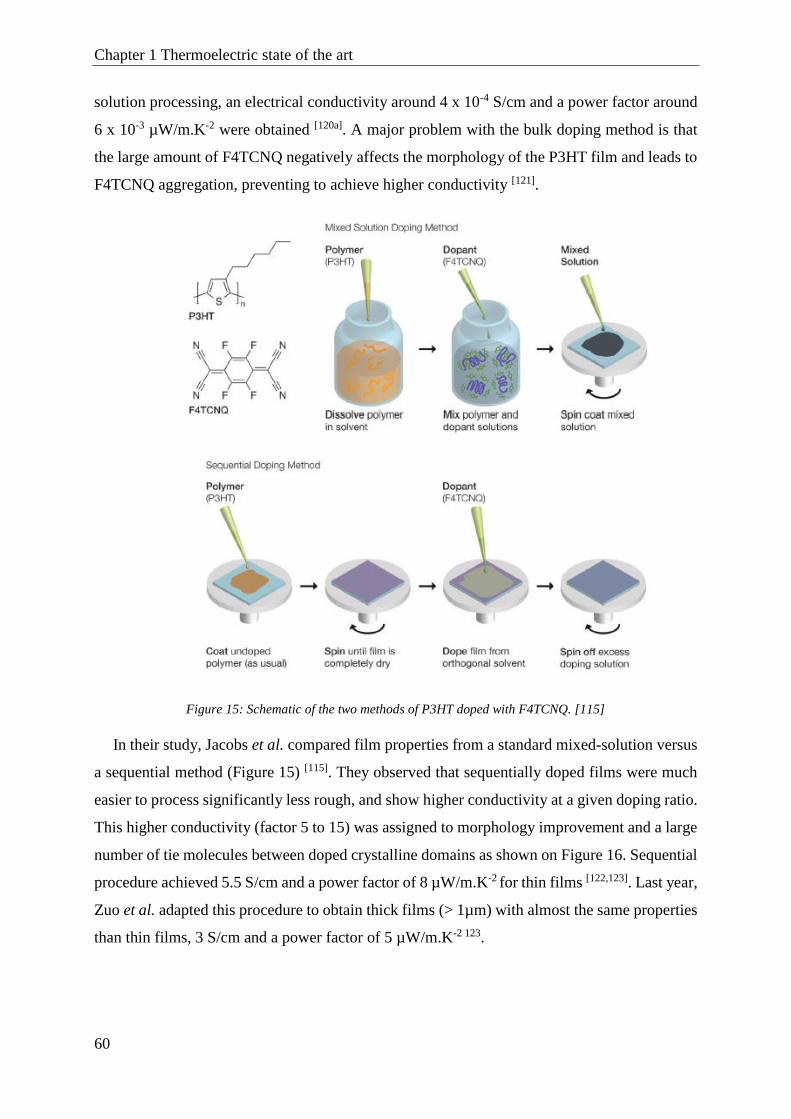
Chapter 1 Thermoelectric state of the art
60
solution processing, an electrical conductivity around 4 x 10⁻⁴ S/cm and a power factor around
6 x 10⁻³ µW/m.K-2 were obtained [120a]. A major problem with the bulk doping method is that
the large amount of F4TCNQ negatively affects the morphology of the P3HT film and leads to
F4TCNQ aggregation, preventing to achieve higher conductivity [121].
Figure 15: Schematic of the two methods of P3HT doped with F4TCNQ. [115]
In their study, Jacobs et al. compared film properties from a standard mixed-solution versus
a sequential method (Figure 15) [115]. They observed that sequentially doped films were much
easier to process significantly less rough, and show higher conductivity at a given doping ratio.
This higher conductivity (factor 5 to 15) was assigned to morphology improvement and a large
number of tie molecules between doped crystalline domains as shown on Figure 16. Sequential
procedure achieved 5.5 S/cm and a power factor of 8 µW/m.K-2 for thin films [122,123]. Last year,
Zuo et al. adapted this procedure to obtain thick films (> 1µm) with almost the same properties
than thin films, 3 S/cm and a power factor of 5 µW/m.K-2 123.
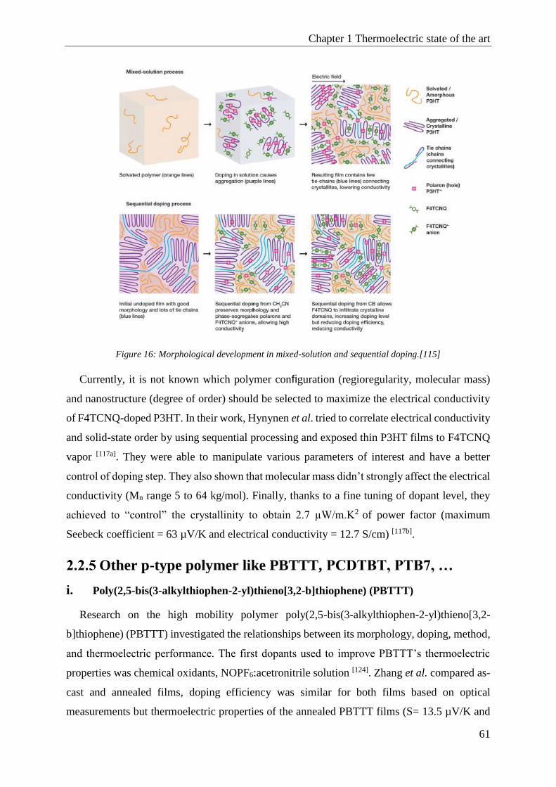
Chapter 1 Thermoelectric state of the art
61
Figure 16: Morphological development in mixed-solution and sequential doping.[115]
Currently, it is not known which polymer configuration (regioregularity, molecular mass)
and nanostructure (degree of order) should be selected to maximize the electrical conductivity
of F4TCNQ-doped P3HT. In their work, Hynynen et al. tried to correlate electrical conductivity
and solid-state order by using sequential processing and exposed thin P3HT films to F4TCNQ
vapor [117a]. They were able to manipulate various parameters of interest and have a better
control of doping step. They also shown that molecular mass didn’t strongly affect the electrical
conductivity (Mn range 5 to 64 kg/mol). Finally, thanks to a fine tuning of dopant level, they
achieved to “control” the crystallinity to obtain 2.7 µW/m.K2 of power factor (maximum
Seebeck coefficient = 63 µV/K and electrical conductivity = 12.7 S/cm) [117b].
Other p-type polymer like PBTTT, PCDTBT, PTB7, …
i. Poly(2,5-bis(3-alkylthiophen-2-yl)thieno[3,2-b]thiophene) (PBTTT)
Research on the high mobility polymer poly(2,5-bis(3-alkylthiophen-2-yl)thieno[3,2-
b]thiophene) (PBTTT) investigated the relationships between its morphology, doping, method,
and thermoelectric performance. The first dopants used to improve PBTTT’s thermoelectric
properties was chemical oxidants, NOPF6:acetronitrile solution [124]. Zhang et al. compared as-
cast and annealed films, doping efficiency was similar for both films based on optical
measurements but thermoelectric properties of the annealed PBTTT films (S= 13.5 µV/K and
Chapter 1 Thermoelectric state of the art
62
σ=55 S/cm) were higher than those of as-cast films (S= 11 µV/K and σ= 33 S/cm). The power
factor in annealed films was three times higher than as-cast films, which was attributed to the
increased structural ordering and domain size [124].
Later, acid dopants like (tridecafluoro-1,1,2,2-tetrahydrooctyl)trichlorosilane (FTS) and
4-ethyl-benzenesulfonic acid (EBSA) were used on PBTTT films [125]. The conductivity of
PBTTT films was increased to similar levels, 1000 S/cm and 1300 S/cm for FTS and EBSA.
However, the two doping agents led to different Seebeck coefficients, 33 µV/K for FTS and
25 µV/K for EBSA. So significantly different power factors were obtained, 110 µW/m.K² for
FTS and 25 µW/m.K² for EBSA, thanks to GIWAXS measurements on PBTTT films shown
that both doping agents generally preserved the edge-on structure of PBTTT crystallites and
that the changes in short-range order could not explain the difference in Seebeck coefficient
[125].
Like for P3HT, F4TCNQ was used for PBTTT and F4TCNQ solution-doped PBTTT has
reached a power factor of 1.3 µW/m.K² [126]. Vapor process with F4TCNQ on PBTTT films
shown a higher power factor of 32 µW/m.K² [127]. The increase resulted from a significant
difference in the electrical conductivity of the films. Vapor-doped films had more than hundred
times increase in conductivity compared to solution-doped films with comparable charge carrier
concentration [126,127]. This increase in conductivity was attributed to both a higher molar ratio
of F4TCNQ in the vapor-doped film. PBTTT was also been doped with 2,5-dufluoro-7,7,8,8-
tetracyanoquinodimethane (F2TCNQ), which has a smaller electron affinity than F4TCNQ.
Due to the lower doping efficiency, the vapor-doped film with F2TCNQ had a lower
conductivity of 36 S/cm and higher Seebeck of 140 µV/K. Despite the lower doping efficiency,
F2TCNQ vapor-doped film had a higher power factor, 70 µW/m.K² than the equivalent
F4TCNQ-doped film [127]. The Seebeck coefficient was not strongly dependent on morphology
at comparable carrier levels. These studies have begun to illuminate the connections between
dopant choice, morphology, and thermoelectric properties in PBTTT and suggest that further
improvement can be realized by increased charge carrier mobility and controlling dopant
concentration [127–129].

Chapter 1 Thermoelectric state of the art
63
ii. Co-polymers
Co-polymerization of donors and acceptors allow for tuning of the electronic properties of
semiconducting polymers. Some efforts have been made to measure and improve the
thermoelectric properties of these donor-acceptor copolymers, doping method, and processing
have not yet been well-explored in this class of polymers.
Several studies on copolymers’ thermoelectric properties have focused on carbazole-
containing copolymers. Copolymers of carbazole and three different acceptors were
synthesized and compared. Poly [N- 9'-heptadecanyl-2,7-carbazole-alt-5,5-(4,7-di-2-thienyl-
2',1',3'-benzothiadiazole] (PCDTBT) films doped with FeCl3 were found to have the highest
power factor, 19 µW/m.K², of the three polymers [130]. Later, the effect of the carbazole unit on
thermoelectric properties was studied by comparing the copolymers poly((9,9-dioctylfluorene)-
2,7-diyl-alt-(4,7-bis(3-hexylthien-5-yl)-2,1,3-benzothiadiazole)-2’,2”-diyl) (F8TBT) and
poly(N-9’-heptadecanyl-2,7-carbazole-alt-(4,7-bis(3-hexyk-thien-5-yl)-2,1,3-benzothiadiazole
-2’,2”-diyl) (C8TBT). F8TBT has a fluorine unit as the donor, while C8TBT has a carbazole
unit. Comparing the properties of these two polymers tests the effect of the nitrogen atom on
the thermoelectric properties. The doped C8TBT films had higher conductivity and Seebeck
coefficient than the doped F8TBT, leading to a higher power factor [131].
More recently, poly2,2′-[(2,5-bis(2-hexyldecyl)-3,6-dioxo-2,3,5,6- tetrahydropyrrolo [3,4-
c] pyrrole-1,4-diyl)dithiophene]- 5,5′-diyl-alt-thiophen-2,5-diyl (PDPP3T) films have
demonstrated a high power factor compared to other thiophene-containing polymers like P3HT
and PBTTT. The power factors of Fe(TFSI)3-doped PDPP3T, P3HT, and PBTTT were
compared [132]. PDPP3T’s optimum power factor of 25 µW/m.K² was higher than PBTTT,
14 µW/m.K², and comparable to P3HT, 30 µW/m.K². Although their power factors were
similar, PDPP3T films had a lower conductivity and higher Seebeck coefficient than other films
even at low doping levels (Figure 17) [89,132]. The optimized power factor obtained for PDPP3T
films was 276 µW/m.K². This great performance was attributed to the smaller volume of
dopants in the PDPP3T films compare to P3HT or PBTTT [133]. This increased power factor
suggests that methods of further improving the thermoelectric properties of donor-acceptor
copolymers will emerge as future research explores this broad class of polymers.

Chapter 1 Thermoelectric state of the art
64
Figure 17: (a) Seebeck coefficient versus the logarithm of electrical conductivity unifying P3HT, PBTTT,
PDPP3T, and PSBTBT. (b) Evolution in the slope S/T with Seebeck coefficients, the slope derived from linear-
fitting of the positive temperature dependence of Seebeck coefficients. [89][132]
n-type “organic” material
N-type polymers have not been as studied for thermoelectric applications as p-type
polymers. The stability of n-type polymers is related to the lowest unoccupied molecular orbital
(LUMO). The LUMO level can be lowered by introducing electron-withdrawing units in the
backbone or as side groups. A couple of n-type organic small molecules were reported, such as
naphthalenetetracarboxylic dianhydride [134], benzotriazole [135], perylene bisimide [136],
naphthodithiophenediimide [137], and fullerenes [138]. The representative n-type thermoelectric
polymer/molecule are presented Figure 18.
N-type doping of polymers is difficult because n-type dopants have small ionization
energies, making them more unstable and vulnerable to reactions with air [139]. Organic donor
molecules, such as 4-(1,3-dimethyl-2,3-dihydro1H-benzoimidazol-2-yl)phenyl)dimethylamine
(N-DMBI) [140a], tetra-n-butyl ammonium fluoride (TBAF) [140b], and cobaltocene (CoCp2) [140c],
were employed to dope these n-type molecules. Development of new types of stable dopants
and polymers with higher miscibility with dopants is currently under investigation [141].

Chapter 1 Thermoelectric state of the art
65
X
X
O O
OO
N
N
HN
NH
HN OO
OO
N
N
S
S
OO
O O
XX
R
R
R: Alkyl groups
X: H, F, Cl, CN
OCH3
O
S
Ni
S
S
S
n
X
. XK
S
S
S
S
S
S
CuCu
Cu
Cu Cu
Cu
X: O
N
N
R
R
OO
OO
S
S
NS
N
NS
N
N
R1
R2 O
O
O
O
O
NO
C18H37
C18H37
R2
R1
C18H37
C18H37
n
n
NN N
N
O O
n
N
N
OO
O O
C10H21
C8H17
C8H17
C10H21
n
C10H21
C12H25 C12H25
C10H21
BBL
P(NDIOD-T2)
BDPPV: R1 = H, R2 = H
CIBDPPV: R1 = Cl, R2 = H
FBPPV: R1 = H, R2 = F
KxNiett
CuBHT
C60PC60BM
R: R:
PNDTI-BBT-DT PNDTI-BBT-DP
NDTI
X: NH, NR
NTCDA
Benzotriazole
Perylene BisimideNDI
Figure 18: Chemical structure of n-types polymers
Chapter 1 Thermoelectric state of the art
66
Heeger was the first to report n-type behavior for polymer (S = -43.5 µV/K) with
polyacetylene doped with TBAF by electrochemical reduction [142]. Conjugated polymers with
metal atoms in the backbone can show n-type behavior and have good air stability [143–147].
Currently the best performance as n-type is an organometallic polymer based on metal-
ethenetetrathiolate (ETT), Poly(Ni-1,1,2,2-ethentetrathiolate) (poly(Ni-ETT)). As a pellet,
poly(Kx(Ni-ETT) reached power factors to 66 µW/m.K² [148], and 344 µW/m.K² in an
electrochemically polymerized poly(Ni-ETT) film [141]. Besides KxNiett, the thermoelectric
performance of other polymers with the Ni-S coordinate bonds, such as copper
benzenehexathiol complex (Cu-BHT), was investigated [149]. Cu-BHT can have a high electrical
conductivity over 1500 S/cm and a Seebeck coefficient of -4 to -10 μV/K. However, these
polymers are insoluble in common solvents and are difficult to process, limiting the ability to
study how they can be further optimized.
Later, Pei and co-workers introduced electron withdrawing elements like Cl and F to
p- phenylene vinylene (PPV) [150]. FBDPPV (fluorine functionalized benzodifurandione-based
poly(p-phenylene vinylele) (FBDPPV) doped with N-DMBI had a power factor of
28 µW/m.K² [151]. Like p-type polymers, n-type polymers thermoelectric properties also depend
on the morphology. Ma et al. investigated the effect of dopant on the crystallinity on FBDPPV
[152]. The GIWAXS indicates that the crystallinity of the polymer varies with the doping level
of N-DMBI. FBDPPV with the optimal doping level can exhibit an electrical conductivity of
6.2 S/cm, a Seebeck coefficient of −210 μV/K and a power factor of 25.5 μW/m.K². ClBDPPV
(chlorine functionalized benzodifurandione-based poly(p-phenylene vinylele) (ClDPPV) doped
with TBAF also demonstrated good air stability for a solution-processed n-type polymer.
Measured in air, doped films had a conductivity of 0.62 S/cm and power factor of
0.63 μW/m.K². After storage in air for one week, films retained a conductivity of 0.1 S/cm [153].
Another group of high-performance solution-processable n-type polymers are the
naphthalenediimide (NDI) copolymers. PolyN,N′-bis(2-octyldodecyl)-1,4,5,8-
napthalenedicarboximide-2,6-diyl]-alt-5,5-(2,2bithiophene) (P(NDIOD-T2) with the
electron-deficient imidazole groups is one of the most famous n-type polymers for
thermoelectric applications. The PNDIOD-T2 polymers in the doped state show better air
stability than PPV derivatives. Additionally, they can be dispersed in organic solvents like
1,2- dichlorobenzene and can be thus processed by solution processing techniques. Chabinyc
et al. investigated this polymer with different dopants including 4-(1,3-dimethyl-2,3-dihydro-
1H-benzimidazol-2-yl)-N,N-diphenylaniline (N-DPBI) and N-DMBI [154]. The optimally doped
Chapter 1 Thermoelectric state of the art
67
film had a power factor of 0.6 μW/m.K². Atomic force microscopy (AFM) images shown that
N-DMBI had largely aggregated on the films surface, only 1% of dopant molecules contributed
a free carrier in the film [154]. These results highlight the importance of dopant-polymer
miscibility in improving the thermometric performance of solution-processable n-type
polymers. Recent studies have tried to improve the miscibility of N-DMBI in PNDIOD-T2 by
replacing the alkyl chains of the NDI unit with PEG chains [155] or by adding polar side chains
to both the NDI and thiophene units [156]. Other studies worked on polymer solubility, inspired
by PVDIOD-T2, copolymers of naphtho[2,3-b:6,7-b]dithiophenediimide (NDTI) and
benzobisthiadiazole (BBT) units like PNDTIBBT-DT and PNDTI-BBT-DP were synthesized
[157]. They exhibit an electrical conductivity of 5 S/cm and a PF of 14 μW/m.K².
Conjugated polymers with ladder structures can have high solubility in organic solvents.
They were investigated as n-type TE polymers. Ladder-type polymers such as
polybenzimidazobenzophenanthroline (BBL) doped with TDAE was reported [158]. Although
its PF is only 0.43 μW/m.K², it is soluble in organic solvents like o-dichlorobenzene. Hence, it
can be processed in large scale like the p-type PEDOT:PSS.
These studies on n-type polymers with dopant show that the most crucial issues in improving
the thermoelectric properties are stability and the miscibility of the dopant in the polymer host.
Afterword on polymer/organic n- & p-type materials
Thermoelectric performance of polymer/organic n- & p-type materials could be summarized
in a graphical (Figure 19). Electrical conductivity and Seebeck coefficient are obviously
dependent on each other, Chabinyc and co-workers [126] suggested the empirical relation
S ∝ σ-1/4 (S²σ ∝ σ1/2) for p-type materials, confirmed by Kemerink and co-workers [121] for
n-type materials. In some cases, another exponent would result in a better fit of the experimental
data. Grey/white lines present a constant figure of merit ZT which was estimated assuming a
phonon contribution to the thermal conductivity of kph = 0.2 /m/K and the Wiedemann-Franz
law is obeyed. So κ follows σ evolution according to the Wiedemann-Franz law. This relation
between κ and σ is a limitation to obtain high ZT value, one possible strategy to surpass it could
be the decoupling of the electronic and thermal conductivity by creating heterogeneous
materials like nanocomposites with inorganic materials that enhance phonon scattering.
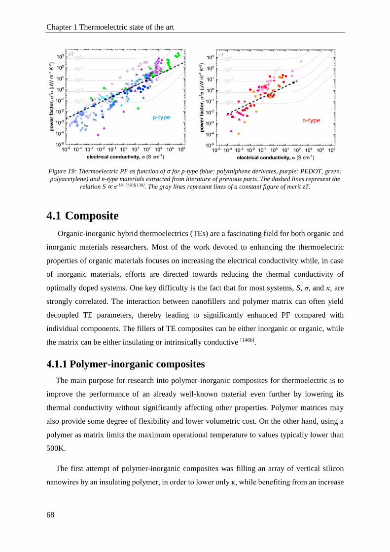
Chapter 1 Thermoelectric state of the art
68
4.1 Composite
Organic-inorganic hybrid thermoelectrics (TEs) are a fascinating field for both organic and
inorganic materials researchers. Most of the work devoted to enhancing the thermoelectric
properties of organic materials focuses on increasing the electrical conductivity while, in case
of inorganic materials, efforts are directed towards reducing the thermal conductivity of
optimally doped systems. One key difficulty is the fact that for most systems, S, σ, and κ, are
strongly correlated. The interaction between nanofillers and polymer matrix can often yield
decoupled TE parameters, thereby leading to significantly enhanced PF compared with
individual components. The fillers of TE composites can be either inorganic or organic, while
the matrix can be either insulating or intrinsically conductive [146b].
Polymer-inorganic composites
The main purpose for research into polymer-inorganic composites for thermoelectric is to
improve the performance of an already well-known material even further by lowering its
thermal conductivity without significantly affecting other properties. Polymer matrices may
also provide some degree of flexibility and lower volumetric cost. On the other hand, using a
polymer as matrix limits the maximum operational temperature to values typically lower than
500K.
The first attempt of polymer-inorganic composites was filling an array of vertical silicon
nanowires by an insulating polymer, in order to lower only κ, while benefiting from an increase
Figure 19: Thermoelectric PF as function of σ for p-type (blue: polythiphene derivates, purple: PEDOT, green:
polyacetylene) and n-type materials extracted from literature of previous parts. The dashed lines represent the
relation S ∝ σ-1/4 [130][138]. The gray lines represent lines of a constant figure of merit zT.

Chapter 1 Thermoelectric state of the art
69
in S due to the reduced dimensionality of the nanowires [159]. Unfortunately, σ strongly
decreased, making an unsuccessful attempt.
Later, PEDOT:PSS was used, instead of an insulating polymer, with ball-milled Bi2Te3, and
power factors of 131 and 80 μW/m.K² for p-type and n-type composites were obtained [160].
While this was an improvement over neat PEDOT:PSS, it remained below the performance of
bulk Bi2Te3, which was attributed to the contact resistance between the components.
In order to understand the increase in thermoelectric performance of polymer-inorganic
material composites, Qiu and col. worked on composites of P3HT and Bi2Te3 nanowires and
cited a doping dependent scattering of carriers as the reason of the improved power factor of
13.6 μW/m.K² [161]. This work suggests an energy-filtering at internal interfaces inducing an
increase in thermoelectric performance of polymer-composite composites. Low energy
charge-carriers are blocked, decreasing σ, otherwise S is increasing because the average energy
carried per charge increases. A study on Te nanowires, PEDOT:PSS and reduced graphene
composite confirms an energy filtering effect occurring at both of the distinct interfaces,
obtaining a power factor of 143 μW/m.K² [162].
On another side, Liang et al. shown that such an effect is not necessarily present. Thanks to
a rigorous control of FeCl3 dopant, they tuned energy barrier between P3HT and
Te- nanoparticles composites by 1eV. This change didn’t affect thermoelectric performance
and they concluded that energy filtering was not mandatory to explain it, a simple linear
combination of parallel and series transport was relevant [163].
Another keypoint in polymer-inorganic composite is thermal conductivity. Conventional
inorganic thermoelectric material possesses high thermal conductivities of
1.2 – 2.8 W/m.K [160,164], nearly one order of magnitude greater than polymers [165]. Thanks to
numerous interfaces in the polymer-inorganic composites, phonons scatters and thermoelectric
composite have a thermal conductivity close to that of the polymer matrix [120,121].
In case of p-type composites, a high ZT of 0.39 was obtained for PEDOT:PSS – Te nanowires
treated with H2SO4 [33]. Authors explained that a structural rearrangement of PEDOT:PSS, due
to the removal of PSS, induced the formation of a more crystalline structure and increased the
number of charge carriers enhancing of electrical conductivity of H2SO4-treated
Te-PEDOT:PSS. For n-type composites, Liang et al. dispersed a large amount of Ni nanowires
inside a PVDF matrix [153] exhibiting an electrical conductivity of 4701 S/cm and Seebeck

Chapter 1 Thermoelectric state of the art
70
coefficient of -20 µV/K, resulting in a power factor of 200 μW/m.K² which is a record for
n-type polymer-inorganic composites.
Polymer-“Carbon” composites
Nanostructured carbon allotropes like carbon nanotubes (CNT) and graphene can also be
used as fillers for thermoelectric composites [166–169]. Their main property is their high electrical
conductivity. Similar to the inorganic/organic thermoelectric composites, the carbon-based
thermoelectric composites have also shown decoupled Seebeck coefficient and electrical
conductivity. Furthermore, the thermal conductivity of the composites still remains low due to
the phonon scattering thus promising thermoelectric performance.
By looking the graphene properties, it’s not an obvious candidate for thermoelectric
application, due to its symmetric density of states without band gap, and its high thermal
conductivity. Nevertheless, Du et al. mixed PANI and graphene nanosheets in pellets and
observed a good power factor of 5.6 μW/m.K², due to a high µ in the composite [120b]. Another
study shown graphene utility in thermoelectric application, Wang and co-workers used
graphene with C60 and PEDOT:PSS to obtained a power factor of 32 μW/m.K² and a ZT of
0.067 [170]. Finally, another promising approach is the interface engineering in multilayer
structures. Promising results were obtained with a layer-by-layer assembly of CNTs and
graphene, stabilized in solution by PEDOT:PSS, and polyaniline which demonstrated power
factor of 1825 μW/m.K² [171] and 2710 μW/m.K² [172]. These high power factors were due to an
increase of mobility and the highly network between multilayers. The same layer-by-layer was
applied to n-type material, and a power factor of 190 μW/m.K² was achieved [173].
Carbon nanotubes are one of the most popular nanofillers for thermoelectric application.
Several approaches to organic thermoelectric CNT composites exist. The basic principles
include electronic percolation, secondary doping (through charge carrier mobility
modifications), energy filtering, interface engineering, improved CNT dispersion and chirality
selection, and multiple strategies for varying charge carrier concentration.
One of the first experiment between CNT and polymers was a simple composite of CNT and
PEDOT:PSS in gum Arabic matrix showing that σ can be partially decoupled from κ [174,175].
The underlying mechanism for this is the fact that electrons are transported through percolative
paths, while heat flows in parallel between the insulating matrix and minute amounts of the
conductive filler. The interfaces between both materials also have a strong influence, as we will

Chapter 1 Thermoelectric state of the art
71
see below. The gum arabic not only decreased κ of the final film, but also stabilized the CNTs
in solution, providing solution-processability. Building on low-κ CNT composites, the gum
arabic has been substituted with conducting and semiconducting polymers.
Later, Grunlan et al. used an optimized PEDOT:PSS – CNTs composites by using single
wall carbon nanotubes (SWCNTs) [176]. They managed to obtain water-processable and flexible
thin films with a low thermal conductivity of 0.4-0.7 W/m.K. A thin film composed of 85 wt%
SWNT achieves a power factor of 140 μW/m.K². The good modulation between CNTs and
polymer matrix was helpful and permitted the formation of highly electrically connecting but
thermally impeding CNT-PEDOT-CNT junctions (Figure 20).
Figure 20: Schematics of CNTs coated by PEDOT:PSS particles in exfoliated state (a) and an electrically
conductive junction formed between CNTs (b). SEM cross-sectional images of 20 w% SWNT film (c) and a 60
wt% SWNT film €. Images (d) and (f) are higher magnification images, marked by dotted boxes. The balance of
each films is PEDOT:PSS. [176]
Post-treatments were also exploited to enhance thermoelectric properties of composites
with CNTs, contributing to enhance more electrical conductivity than Seebeck coefficient. For
example, formic acid and DMSO were used to treat SWCNT/PEDOT:PSS composite [177].

Chapter 1 Thermoelectric state of the art
72
Thanks to this treatment, at the same CNT loading, films treated by DMSO and formic acid
shown an enhancement of power factor over 300 (464 and 407 μW/m.K²).
Composites were prepared directly by synthesizing conducting polymers in presence of
carbon fillers. Such synthesis is known as “template-directed in situ polymerization”, thanks to
the strong π-π interaction between the carbon lattice and the conjugated polymer backbone. A
series of studies on the direct synthesis of carbon-based thermoelectric composites was done by
Chen et al.. They performed the in situ polymerization of monomers, like EDOT [178], pyrrole
[179a], and tried various shapes, such as pie-like [178] and cable-like [179b] (Figure 21).
Their results indicate that the carbon nanofillers, the thickness of surface coating layers as
well as the nanostructures of the conducting polymers can affect the thermoelectric performance
of the composites. Additionally, of the contribution on thermoelectric properties, carbon
nanofillers assist the alignment of the polymer chains and thus increase also the thermoelectric
Figure 21: SEM images of (A) reduced graphene oxide (rGO) sheets & (B) PEDOT-rGO oxide [178]
SEM images MWCNT/Te nanorad composites with MWCNT contents (C) 1 wt%, (D) 3 wt% and (E) 5 wt% [179]

Chapter 1 Thermoelectric state of the art
73
properties. Composites of carbon fillers and PANi were prepared via an in situ polymerization
process [180,181], both of them shown higher Seebeck coefficient and power factors than neat
PANi. Pristine PANi films had a power factor of 5 μW/m.K² while the composite one exhibited
a power factor of 20 μW/m.K². Carbon fillers cause the PANi chains to align in a more ordered
manner as revealed by SEM, XRD, and Raman spectra (Figure 22).
Polymer-Polymer composite
Thermal conductivity being a problem for composite materials, scientists investigated
nanostructured polymers as nanofillers for thermoelectric composites. Thanks to the polymeric
nature of both the filler and matrix, a low thermal conductivity should be achieved. One of the
most used nanostructured polymers is PEDOT nanowires inside PEDOT matrix. By adding, a
few amount, 0.2 w% of PEDOT nanowires, composites can show a high power factor of
446.6 μW/m.K² with a Seebeck coefficient of 59.3 µV/K and σ = 1270 S/cm [182]. This high
power factor could be attributed to an interfacial energy filtering effect arising from the
interface (Figure 23).
Figure 22: (A) SEM image of SWNT/PANi composites with 25 wt% SWNT. (B) XRD patterns for SWNT/PANi
composites with different SWNT content (solid lines and dashed lines denote the peaks of PANi and SWNT).
(C) Raman spectra for SWNT/PANi composites with different SWNT content [181][182]

Chapter 1 Thermoelectric state of the art
74
Furthermore, blending two semiconducting polymers with different HOMO levels, the
density of states can be engineered by adding states close to Fermi level. An energy barrier is
introduced, decreasing σ and acts more effectively on the density of state with respect to energy,
leading to an increase in Seebeck coefficient [120]. To confirm the proposed mechanism, a blends
of P3HT and PTB7 or TQ1 were done and were obtained record values of Seebeck coefficient
near 1 mV/K [183]. This mechanism was also demonstrated on n-types blends of PCBM [184].
Thermoelectric devices (TEG)
5.2 Applications
The field of applications of thermoelectrics is large. Conversion of heat into electricity could
be used in various sectors, like health, defense, electronics, industry, renewable energy and
others. However, low ZT value is the main drawback of thermoelectricity to be spread
everywhere. Since 2014, thermoelectric generators have gained a lot of interest with benefits
around 40 million of US dollar [185], and in only two years benefits doubled to achieve 90 million
of US dollar. IDTechEx expects an annual benefit of 1 billion of US dollar in 2026 for
thermoelectric generators [185].
Internet of things will have a huge impact on technologies market, industries and society.
Wireless connected sensors will have more than billion interconnections with device and
objects. So sophisticated and ubiquitous networks in permanent communication will appear,
requiring more and more data to have an information with more precision, this phenomenon is
called Big Data. In 2020, more than 25 billion devices will be connected [186] requiring billions
of energy source.
Figure 23: AFM topography images of PEDOT NWs/PEDOT :PSS hybrid films with various PEDOT NW weight
fractions. (a) 0.1 wt%, (b) 0.2 wt%, (c) 0.5 wt%, (d) 1 wt% [182].

Chapter 1 Thermoelectric state of the art
75
Thermoelectric generators based on polymer could be one of this energy source with lots of
advantages:
o Flexibility and adaptability to sensor size;
o Maintenance not necessary;
o Lifetime;
o Compatibility with environment;
So Internet of thing could propel thermoelectricity from niche area to major market.
5.3 TEG polymer-based
Thermoelectric devices can be fabricated in vertical (bulk) or in lateral (thin films form).
The first thermoelectric device made with polymers used PEDOT:Tos as the p-type material
and TTF-TCNQ as the n-type in a bulk configuration. Bubnova et al. fabricated this first organic
thermoelectric module producing 0.128 µW with a temperature gradient of 10 K at room
temperature [44]. Later, others studies tried to utilize polymers for thermoelectric devices,
unfortunately, because n-type poor stability and efficiency, most reported devices used only
p- type thermoelectric interconnected in-series with metal paste like silver. Obviously, this kind
of devices shown lower efficiency than p-type/n-type configuration, but by managing the
number of legs and the device architecture, comparable results could be obtained.
Based on this model, screen printed thermoelectric devices on paper made with PEDOT:PSS
and silver connection, obtained a power output of 4 µW in a ΔT = 50 K [187]. Later, a
thermoelectric device, using PEDOT:PSS, was fabricated by thermal lamination at 373 K,
exhibiting a power output of 37 µW in a ΔT = 50 K at room temperature [188a]. The importance
of device architecture was further explored by Lee et al. [188b]. The authors compared the power
output of a vertical (drop-cast, thick film), and a horizontal (spin-coated, thin film) device.
Vertical thermoelectric device had up to 7 times higher power (175 nW @ ΔT = 50K) than
horizontal one. Cho et al. developed a flexible organic thermoelectric generator with
PEDOT:PSS in a chevron-structure (Figure 24) [189]. They managed to integrate 24 PEDOT:PSS
patterns with a high flexibility and obtained a power output of 1 µW at Δ=17.5 K in vertical
heat flow.

Chapter 1 Thermoelectric state of the art
76
Gordiz et al. suggested that a large number of thermoelectric legs would result in high
interconnect resistance that could eventually limit the device output [190]. By positioning the
thermoelectric legs in a hexagonal closed-packed layout, higher fill factor can be achieved that
lower the interconnect resistance and lead to higher power outputs.
Menon et al. proposed a new architecture, a radial thermoelectric device for polymer
thermoelectric device working under natural heat convection [190,191]. Authors managed to
produce 85 mV open circuit voltage and a power density of 15 nW/cm². Later, PEDOT:PSS
was coated on commercial fabrics [192] and silk yarn [193] to make more applicable polymer
thermoelectric devices. In the first study, wearable devices generated a voltage output of
4.3 mV at ΔT = 75 K. Meanwhile, the second one device with 26 legs gave an output voltage
of 35 mV at ΔT = 66 K. Li et al. [194] highlighted the importance of polymer structure to the
performance of a polymer thermoelectric device. In fact, by controlling the structure of free
standing PEDOT:PSS films, the authors reported a 5-leg module with thermo-voltage of 2 mV
at a temperature difference of 25 K.
Finally, photolithography method was used to fabricate a flexible organic module [195].
PEDOT:PSS and TTF-TCNQ were used as the p- & n-type materials. An output voltage of
250 mV, sufficient to drive electrical devices with a booster circuit, was realized at 80 K
temperature difference (Figure 25). However, the high contact resistance was a problem, and it
was proposed to design thermoelectric materials from the standpoints of expected module
structures and mass-production processes rather than optimize ZT of the material first [195].
Figure 24: Schematic description of the fabrication process of a chevron-structured TEG. [189]

Chapter 1 Thermoelectric state of the art
77
5.4 TEG polymer-inorganic composite
Various thermoelectric modules have been fabricated using organic-inorganic hybrid
materials, due to the advantages of flexibility that are conferred by the organic material and
high performance of inorganic material. In a slightly unusual device structure, flexible
transparent modules were reported, by using polyethylene terephthalate (PET) substrate onto
which, PEDOT:PSS and a hybrid indium tin oxide (ITO)-PEDOT:PSS material were deposited
as the p- & n-type legs, respectively. From 8 p-n pairs, a voltage output of 6.8 mV and power
output of 0.86 nW are generated with a temperature difference of around 20 K. The n-type
thermoelectric properties appear dominated by the ITO with no enhancement from the hybrid
effect, however, the authors propose that the PEDOT:PSS coating on top of ITO promotes
mechanical stability during the active bending of the module [196] .
Ferhat et al. made a flexible thermoelectric device on paper entirely fabricated using inkjet
printing. They used PEDOT:PSS as p-type and (TiS2(HA)x) as n-type legs, and obtained a
power output of 22.5 nW at Δ= 20 K for a small device area of 128 mm² [197]. Koumoto and
coworkers have fabricated a thermoelectric module composed of hybrid TiS2/organic
superlattice films and PEDOT:PSS film, as the n- and p-type materials, respectively. From five
p-n pairs, they obtain a voltage output of 33 mV with a maximum power density of 250 μW/cm2
under a temperature difference of 70 K [198].
Figure 25: Photograph and schematic image of the module. [195]
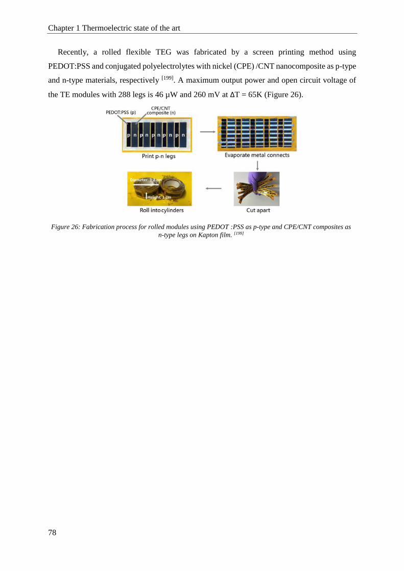
Chapter 1 Thermoelectric state of the art
78
Recently, a rolled flexible TEG was fabricated by a screen printing method using
PEDOT:PSS and conjugated polyelectrolytes with nickel (CPE) /CNT nanocomposite as p-type
and n-type materials, respectively [199]. A maximum output power and open circuit voltage of
the TE modules with 288 legs is 46 µW and 260 mV at ΔT = 65K (Figure 26).
Figure 26: Fabrication process for rolled modules using PEDOT :PSS as p-type and CPE/CNT composites as
n-type legs on Kapton film. [199]

Chapter 1 Thermoelectric state of the art
79
C Conclusion
Thermoelectricity is not a new phenomenon, nevertheless for the production of electricity,
it knows for ten years a renewed interest. Indeed, the direct conversion of heat into electricity
by the thermoelectric modules makes it possible to limit both the number and the complexity
of the elements that make up the TEG. It is, therefore, one of the most robust energy conversion
systems.
On the other hand, the field of thermoelectric polymers can still be considered in its infancy
with respect to the thermoelectric inorganic domain. Most reported studies involved p-type
materials, and the optimization of their thermoelectric properties. The keystone of this
optimization lies in the ability to fine-tuning to the electronic properties of materials via doping.
This challenge is the main axis of research for many groups as revealed by this state of the art.
Furthermore, for a fully functional thermoelectric generator, an n-type material is also
needed. To overcome the limited thermoelectric performance and stability of n-type material,
inorganic/organic composite could be developed. This alternative shown a high potential to
modulate the thermoelectric behavior from n-type material.
Finally, development for the fabrication of fully operational thermoelectric generator is
necessary. The evaluation of the Power Output delivered by such devices is crucial to evaluate
the “organic thermoelectric” technology.
The objective of this thesis work is to create a performant TEG for near room temperature.
As shown in this Chapter 1, polymers appeared as great candidates for thermoelectric
applications thanks to a unique combination of properties. It is essential to properly characterize
the thermoelectric properties of polymer material, and then enhance them by a fine tuning of
electronic structure with doping. Chapter 2 described thermoelectric properties optimization of
several famous polymers such as PEDOT:Tos, P3HT, PCDTBT and PTB7. Moreover, various
n-type materials were studied, particularly a n-type polymer from Prof. Jenekhe’s group, a
naphthalenediimide-biselenophene copolymer (PNDIBS). Then, in order to continue to
improve thermoelectric properties, a novel approach designed in our laboratory, coupling
inorganic semi-conducting substrate and organic materials, was developed (Chapter 3). The
interface between inorganic and organic material was studied, and the surface of the inorganic
substrate was etched to increase its specific surface area (Chapter 4). Silicon was chosen as
Chapter 1 Thermoelectric state of the art
80
inorganic semi-conducting substrate due to its high importance in electronic and industrial field,
its high range of impurities concentration (doping concentration) accessible and its good
thermoelectric properties (S ≈ 500-1200 µV/K when correctly doped) at room temperature.
Resulting hybrid silicon-polymer devices exhibit a significate improvement of thermoelectric
properties. These “novel” hybrid materials were used as building block for the fabrication of
performant TEG (Chapter 5).

Chapter 1 Thermoelectric state of the art
81
References
[1] L. I. Anatychuk, Journal of thermoelectricity No2, 2004, 5–11 (ISSN 1607-8829).
[2] T. J. Seebeck, Magnetische Polarisation der Metalle und Erze durch Temperature
Differenz, Leipzig, W. Engelmann, « Ostwald’s Klassiker Exakten Wissenschaften
vol.70 », 1895, 120 p.
[3] H. C. Ørsted, Der Geist in der Natur, München, Cotta, 1850.
[4] G. Magnus, Poggendorf’s Annalen der Physik, « Poggendorfs Ann. Phys vol.83 ».
1851, 469 p.
[5] J. C. Peltier, Nouvelles expériences sur la caloricité des courants électriques, « Ann.
Chim vol. I. IV. », 1834, 371–87.
[6] E. Lenz, Ueber einige Versuche im Gebiete des Galvanismus, St. Pétersb. « Acaf. Sci.
Bull, Ann. Phys. vol. III », 1838, 120, 342 p.
[7] J. P. J. Esq, On the heat evolved by metallic conductors of electricity, and in the cells
of a battery during electrolysis, Dublin, Lond. Edinb., « Philos. Mag. J. Sci. 3 » 1841,
19, 260 p.
[8] W. Thomson, On the Dynamical Theory of Heat Transfer, Edinburgh, Earth Environ.
Sci. Trans. R. Soc. Edinb. 1853, 20, 261 p.
[9] E. Altenkirch, Physikalische Zeitschrift, 1991, 12, 120.
[10] W. Brostow, G. Granowski, N. Hnatchuk, J. Sharp, J. White, J. Mater. Educ. 2014,
36, 175.
[11] C. Kittel, Introduction to Solid State Physics, Wiley India Pvt. Limited, « Seventh
Edition », 2007.
[12] M. V. Vedernikov, E. K. Iordanishvili, In Seventeenth International Conference on
Thermoelectrics. Proceedings ICT98 (Cat. No.98TH8365); IEEE: Nagoya, Japan,
1998; pp. 37–42.
[13] G. S. Nolas, J. Sharp, J. Goldsmid, Thermoelectrics: Basic Principles and New
Materials Developments, Berlin Heidelberg, Springer Series in Materials Science, «
Springer-Verlag », 2001.
[14] D. M. Rowe, Thermoelectrics Handbook: Macro to Nano, « CRC Press Book », 2006.
[15] P. R. Sangi Reddy, PhD Thesis: Transport of charge and energy in metal-molecule-
metal junctions, Univ. of California, Berkeley, 2007.
[16] R. Y.-S. Wang, PhD Thesis: Energy transport and conversion in nanostructured
materials, Univ. of California, Berkeley, 2008.
[17] S. K. Yee, PhD Thesis: Development of Organic-Inorganic Hybrid Thermoelectrics,
Univ. of California, Berkeley, 2013.
[18] G. J. Snyder, E. S. Toberer, Natur. Mater., 2008, 7, 105-114
[19] C. Uher, Material Aspect of Thermoelectricity, « CRC Press Book », 2016.
[20] H. J. Goldsmid, Introduction to Thermoelectricity, Berlin, Heidelberg, « Springer
Series in Materials Science », 2010, pp. 7–21.
[21] А. F. Ioffe, Semiconductor thermoelements, and Thermoelectric cooling, London, «
Infosearch First ed. », 1957.
[22] D. M. Rowe, Handbook of Thermoelectrics., « CRC Press Book », 1995.
[23] T. Caillat, J. Sakamoto, A. Jewell, C.-K. Huang, J. Cheng, J. Paik, P. Gogna, P.-J.
Fleurial, R. Ewell, “Status of skutterudite-based segmented thermoelectric technology
components development at JPL”, in STAIF 23rd Symposium on Space Nuclear Power
and Propulsion, Albuquerque, New Mexico, 2006.
Chapter 1 Thermoelectric state of the art
82
[24] T. Caillat, S. Firdosy, S. C. B. Li, J.-A. Paik, C.-K Huang, J. Cheng, J.-P. Fleurial, V.
Ravi, E. J. Brandon, “Advanced high-temperature thermoelectric devices”, in DOE
Thermoelectric Applications Workshop, 2009.
[25] R. L. Cataldo, G. L. Bennett, Radioisot. - Appl. Phys. Sci. 2011.
[26] B. Russ, A. Glaudell, J. J. Urban, M. L. Chabinyc, S. Segalman, Nature Reviews
Materials, 2016, 1.
[27] S. M. Haque, J. A. A. Rey, A. A. Masud, Y. Umar, R. Albarracin, Electrical Properties
of Different Polymeric Materials and their Applications: The Influence of Electric
Field Chapter 3, Boxue Du, « IntechOpen », 2017, 25 p.
[28] A. B. Robbins, A. J. Minnich, Appl. Phys. Lett. 2015, 107, 201908.
[29] C. L. Choy, Polymer 1977, 18, 984.
[30] C. L. Yaws, Viscosity, Thermal Conductivity, and Diffusivity of C1 to C100 Organics
and Ac to Zr Inorganics, « Transport Properties of Chemicals and Hydrocarbons - 1st
Edition », 2009, pp. 403-406.
[31] M. Culebras, C. M. Gómez, A. Cantarero, Materials 2014, 7, 6701.
[32] M. Orrill, S. LeBlanc, J. Appl. Polym. Sci. 2017, 134.
[33] E. J. Bae, Y. H. Kang, K.-S. Jang, S. Y. Cho, Sci. Rep. 2016, 6, 18805.
[34] S. Hwang, W. J. Potscavage, R. Nakamichi, C. Adachi, Org. Electron. 2016, 31, 31.
[35] C. K. Chiang, C. R. Fincher, Y. W. Park, A. J. Heeger, H. Shirakawa, E. J. Louis, S.
C. Gau, A. G. MacDiarmid, Phys. Rev. Lett. 1977, 39, 1098.
[36] H. Shirakawa, E. J. Louis, A. G. MacDiarmid, C. K. Chiang, and A. J. Heeger, Journal
of the Chemical Society, Chemical Communications, 1977, 578.
[37] W. P. Su, J. R. Schrieffer, A. J. Heeger, Phys. Rev. Lett. 1979, 42, 1698.
[38] (a) W. P. Su, J. R. Schrieffer, A. J. Heeger, Physical Review B, 1980, 22, 2099. (b) Y.
Xuan, Phys. Rev. B, 2010, 82, 115454-9.
[39] W. P. Su, J. R. Schrieffer, Proc. Natl. Acad. Sci. U. S. A. 1980, 77, 5626.
[40] Y. W. Park, A. Denenstein, C. K. Chiang, A. J. Heeger, A. G. MacDiarmid, Solid State
Commun. 1979, 29, 747.
[41] Y. Hiroshige, M. Ookawa, N. Toshima, Synthetic Metals, 2007, 157, 467-474.
[42] M. Scholdt, H. Do, J. Lang, A. Gall, A. Colsmann, U. Lemmer, J. D. Koenig, M.
Winkler, H. Boettner, J. Electron. Mater. 2010, 39, 1589.
[43] L. Groenendaal, F. Jonas, D. Freitag, H. Pielartzik, J. R. Reynolds, Advanced
Materials, 2000, 12, 481.
[44] O. Bubnova, Z. U. Khan, A. Malti, S. Braun, M. Fahlman, M. Berggren, X. Crispin,
Nat. Mat., 2011, 10, 429-433.
[45] S. Kirchmeyer, K. Reuter, J. Mater. Chem. 2005, 15, 2077.
[46] A. Elschnet, S. Kirchmeyer, W. Lovenich, U. MErker, K. Reuter, PEDOT: Principles
and Applications of an Intrinsically Conductive Polymer, Boca Raton, FL, USA, «
CRC Press Book », 2010.
[47] Y. Xia, J. Ouyang, ACS Appl. Mater. Interfaces 2012, 4, 4131.
[48] J. Ouyang, ACS Appl. Mater. Interfaces 2013, 5, 13082.
[49] J. Luo, D. Billep, T. Waechtler, T. Otto, M. Toader, O. Gordan, E. Sheremet, J. Martin,
M. Hietschold, D. R. T. Zahn, T. Gessner, J. Mater. Chem. A 2013, 1, 7576.
[50] J. Xiong, F. Jiang, W. Zhou, C. Liu, J. Xu, RSC Adv. 2015, 5, 60708.
[51] S. Liu, H. Deng, Y. Zhao, S. Ren, Q. Fu, RSC Adv. 2014, 5, 1910.
[52] L. Zhang, H. Deng, S. Liu, Q. Zhang, F. Chen, Q. Fu, RSC Adv. 2015, 5, 105592.
[53] S. Zhang, Z. Yu, P. Li, B. Li, F. H. Isikgor, D. Du, K. Sun, Y. Xia, J. Ouyang, Org.
Electron. 2016, 32, 149.
[54] Y. Xia, J. Fang, P. Li, B. Zhang, H. Yao, J. Chen, J. Ding, J. Ouyang, ACS Appl. Mater.
Interfaces 2017, 9, 19001.

Chapter 1 Thermoelectric state of the art
83
[55] F. Kong, C. Liu, H. Song, J. Xu, Y. Huang, H. Zhu, J. Wang, Synth. Met. 2013, 185–
186, 31.
[56] C. Yi, A. Wilhite, L. Zhang, R. Hu, S. S. C. Chuang, J. Zheng, X. Gong, ACS Appl.
Mater. Interfaces 2015, 7, 8984.
[57] D. A. Mengistie, C.-H. Chen, K. M. Boopathi, F. W. Pranoto, L.-J. Li, C.-W. Chu,
ACS Appl. Mater. Interfaces 2015, 7, 94.
[58] K. Sun, S. Zhang, P. Li, Y. Xia, X. Zhang, D. Du, F. H. Isikgor, J. Ouyang, J. Mater.
Sci. Mater. Electron. 2015, 26, 4438.
[59] Y. Xia, K. Sun, J. Chang, J. Ouyang, J. Mater. Chem. A 2015, 3, 15897.
[60] H. Shi, C. Liu, Q. Jiang, J. Xu, Adv. Electron. Mater. 2015, 1,1500017.
[61] Z. Yu, Y. Xia, D. Du, J. Ouyang, ACS Appl. Mater. Interfaces 2016, 8, 11629.
[62] Z. FAn, D. DU, Z. Yu, P. Li, Y. XIa, J. Ouyang, ACS Appl. Mater. Interfaces, 2016,
8, 23204
[63] S. Zhang, Y. Xia, J. Ouyang, Org. Electron., 2017, 45, 139.
[64] D. M. De Leeuw, P. A. Kraakman, P. F. G. Bongaerts, C. M. J. Mutsaers, D. B. M.
Klaassen, Synth. Met. 1994, 66, 263–273.
[65] G. Heywang, F. Jonas, Adv. Mater., 1992, 4, 116-118.
[66] M. Fabretto, K. Zuber, C. Hall, P. Murphy, Macromol. Rapid Commun, 2008, 29,
1403-1409.
[67] M. Fabretto, C. Jariego-Moncunill, J. -P. Autere, Polymer, 2011, 52, 1725-1730.
[68] B. Winther-Jensen, O. Winter-Jensen, M. Forsyth, D. R. MacFarlane, Science, 2008,
321, 671-674.
[69] R. Noriega, J. Rivnay, K. Vandewal, F. P. V. Koch, N. Stingelin, P. Smith, M. F.
Toney, A. Salleo, Nat. Mater. 2013, 12, 1038.
[70] I. Petsagkourakis et al., Scientific Reports, 2016, 6:30501.
[71] A. B. Kaiser, V. Skákalová, Chem. Soc. Rev. 2011, 40, 3786.
[72] O. Bubnova et al., Nat. Mater. 2014, 13, 190.
[73] I. Petsagkourakis et al., Organic Electronics, 2018, 52, 335-341
[74] J. Y. Kim, J. H. Jung, D. E. Lee, J. Joo, Synth. Met. 2002, 126, 311.
[75] C. Liu, B. Lu, J. Yan, J. Xu, R. Yue, Z. Zhu, S. Zhou, X. Hu, Z. Zhang, P. Chen, Synth.
Met. 2010, 160, 2481.
[76] F.-F. Kong, C.-C. Liu, J.-K. Xu, F.-X. Jiang, B.-Y. Lu, R.-R. Yue, G.-D. Liu, J.-M.
Wang, Chin. Phys. Lett. 2011, 28, 037201.
[77] G. H. Kim, L. Shao, R. Zhang, K. P. Pipe, Nat. Mater, 2013, 12, 719-723.
[78] C. M. Palumbiny et al., Adv. Mater., 2015, 27, 3391-3397.
[79] E. Liu, C. Liu, Z. Zhu, H. Shi, Q. Jiang, F. Jiang, J. Xu, J. Xiong, Y. Hu, J. Polym.
Res. 2015, 22, 240.
[80] N. Kishi, Y. Kondo, H. Kunieda, S. Hibi, Y. Sawada, J. Mater. Sci. Mater. Electron.
2018, 29, 4030.
[81] J. Wang, K. Cai, S. Shen, Organic Electronics, 2014, 15, 3087-3095.
[82] D. Beretta et al., ACS Appl. Mater. Interfaces, 2017, 9, 18151-18160.
[83] H. Yu, Soft Materials, 2018, 16:1, 31-36.
[84] S. H. Lee, H. Park, W. Son, H. H. Choi, J. H. Kim, J. Mater. Chem. A, 2014, 2, 13380.
[85] N. Massonnet, A. Carella, O. Jaudouin, P. Rannou, G. Laval, C. Celle, J.-P. Simonato,
J. Mater. Chem. C, 2014, 2, 1278.
[86] Z. U. Khan, O. Bubnova, M. J. Jafari, R. Brooke, X. Liu, R. Gabrielsson, T. Ederth,
D. R. Evans, J. W. Andreasen, M. Fahlman, X. Crispin, J. Mater. Chem. C, 2015, 3,
10616.
[87] Z. Fan, P. Li, J. Ouyang, Advanced Energy Materials, 2017, 7, 1602116.

Chapter 1 Thermoelectric state of the art
84
[88] K. Gurunathan, A. V. Murugan, R. Marimuthu, U. P. Mulik, D. P. Amalnerkar, Mater.
Chem. Phys., 1999, 61, 173.
[89] L. Zhang, T. Goto, I. Imae, Y. Sakurai, Y. Harima, J. Polym. Sci. Part B Polym. Phys.,
2017, 55, 524.
[90] T. Park, C. Park, B. Kim, H. Shin, E. Kim, Energy Environ. Sci., 2013, 6, 788.
[91] O. Bubnova, M. Berggren, X. Crispin, J. Am. Chem. Soc., 2012, 134, 16456-16459.
[92] J. L. Bredas, G. B. Street, Accounts of Chemical Research, 1985, 18, 309.
[93] N. Basescu, Z.-X. Liu, D. Moses, A. J. Heeger, H. Naarmann, N. Theophilou, Nature,
1987, 327, 403.
[94] R. Zuzok, A. B. Kaiser, W. Pukacki, S. Roth, J. Chem. Phys., 1991, 95, 1270.
[95] Y. W. Park, C. O. Yoon, B. C. Na, H. Shirakawa, K. Akagi, Synth. Met., 1991, 41, 27.
[96] H. Kaneko, T. Ishiguro, A. Takahashi, J. Tsukamoto, Synth. Met. 1993, 57, 4900.
[97] Y. W. Park, Y. S. Lee, C. Park, L. W. Shacklette, R. H. Baughman, Solid State
Commun., 1987, 63, 1063.
[98] Y. W. Park, J. S. Moon, M. K. Bak, J.-I. Jin, Synth. Met,. 1989, 29, 389.
[99] E. Dalas, S. Sakkopoulos, E. Vitoratos, J. Mater. Sci., 1994, 29, 4131.
[100] S. Bhadra, N. K. Singha, and D. Khastgir, Science, 2007, 104, 1900.
[101] B. Abad et al., Journal of Materials Chemistry A, 2013, 1, 10450-7.
[102] H. Yan, N. Sada, N. Toshima, J. Therm. Anal. Calorim. 2002, 69, 881.
[103] J. Li, X. Tang, H. Li, Y. Yan, Q. Zhang, Synth. Met. 2010, 160, 1153.
[104] C. Nath, A. Kumar, Y. -K. Kuo, G. S. Okram, Appl. Phys. Lett., 2014, 105, 133108-5.
[105] Y. Yang, S. Chen, L. Xu, Macromol. Rapid Commun. 2011, 32, 593.
[106] S. P. Armes, Synth. Met. 1987, 20, 365.
[107] P. Jha et al., Macromolecules, 2011, 44, 4583-5.
[108] G. Qi, L. Huang, H. Wang, Chem. Commun. 2012, 48, 8246.
[109] D. Oukil et al., Sensors and Actuators B: Chemical, 2014, 204¸203.
[110] N. T. Kemp, A. B. Kaiser, C.-J. Liu, B. Chapman, O. Mercier, A. M. Carr, H. J.
Trodahl, R. G. Buckley, A. C. Partridge, J. Y. Lee, C. Y. Kim, A. Bartl, L. Dunsch,
W. T. Smith, J. S. Shapiro, J. Polym. Sci. Part B Polym. Phys. 1999, 37, 953.
[111] M. Culebras, B. Uriol, C. M. Gomez, A. Cantarero, Phys. Chem., 2015, 17, 15140-5.
[112] B. Endrdi et al., J . Chem. C, 2015, 119, 8472-9.
[113] Q. Zhang, Y. Sun, W. Xu, D. Zhu, Energy Environ. Sci. 2012, 5, 9639.
[114] D. T. Duong, H. Phan, D. Hanifi, P. S. Jo, T.-Q. Nguyen, A. Salleo, Adv. Mater.
Deerfield Beach Fla 2014, 26, 6069.
[115] I. E. Jacobs, E. W. Aasen, J. L. Oliveira, T. N. Fonseca, J. D. Roehling, J. Li, G. Zhang,
M. P. Augustine, M. Mascal, A. J. Moulé, J. Mater. Chem. C 2016, 4, 3454.
[116] C. Wang, D. T. Duong, K. Vandewal, J. Rivnay, A. Salleo, Phys. Rev. B 2015, 91,
085205.
[117] (a) J. Hynynen et al., 2017, 50, 8140-8148. (b) E. Justin et al., Macromolecules, 2014,
47 (19), 6836-6846.
[118] E. J. Cochran et al., Macromolecules, 2014, 47 (19), 6836-6846.
[119] D. T. Duong, C. Wang, E. Antono, M. F. Toney, A. Salleo, Org. Electron. 2013, 14,
1330.
[120] (a) J. Sun et al., Macromolecules, 2010, 43 (6), 2897-2903. (b) Y. Du et al., Synth.
Met., 2012, 161, 2688-2692.
[121] G. Zuo et al., J. Phys. Chem. C, 2017, 121 (14), 7767-7775.
[122] D. T. Scholes, S. A. Hawks, P. Y. Yee, H. Wu, J. R. Lindemuth, S. H. Tolbert, B. J.
Schwartz, J. Phys. Chem. Lett. 2015, 6, 4786.
[123] G. Zuo, O. Andersson, H. Abdalla, M. Kemerink, Appl. Phys. Lett. 2018, 112, 083303.
[124] Q. Zhang, Y. Sun, F. Jiao, J. Zhang, W. Xu, D. Zhu, Synth. Met. 2012, 162, 788.

Chapter 1 Thermoelectric state of the art
85
[125] Q. Zhang, Macromolecules, 2014, 47 (2), 609-615.
[126] A. M. Glaudell, J. E. Cochran, S. N. Patel, M. L. Chabinyc, Adv. Energy Mater., 2014,
5 (4), 1401072.
[127] S. N. Patel, A. M. Glaudell, K. A. Peterson, E. M. Thomas, K. A. O’Hara, E. Lim, M.
L. Chabinyc, Sci. Adv. 2017, 3, e1700434.
[128] E. Lim, K. A. Peterson, G. M. Su, M. L. Chabinyc, Chem. Mater. 2018, 30, 998.
[129] S. N. Patel, A. M. Glaudell, D. Kiefer, M. L. Chabinyc, ACS Macro Lett. 2016, 5, 268.
[130] R. B Aïch, N. Blouin, A. Bouchard, M. Leclerc, Chem. Mater., 2009, 21 (4), 751-757
[131] L. Wang, C. Pan, A. Liang, X. Zhou, W. Zhou, T. Wan, L. Wang, Polym. Chem. 2017,
8, 4644.
[132] Q. Zhang, Y. Sun, W. Xu, D. Zhu, Macromolecules 2014, 47, 609.
[133] I. H. Jung et al., Scientific Reports, 2017, 7, 44704.
[134] A. Nollau, M. Pfeiffer, T. Fritz, K. Leo, J. Appl. Phys. 2000, 87, 4340.
[135] (a) W. W. H. Wong, J. Subbiah, S. R. Puniredd, W. Pisula, D. J. Jones, A. B. Holmes,
Polym. Chem. 2014, 5, 1258. (b) J. L. Banal, J. Subbiah, H. Graham, J.-K. Lee, K. P.
Ghiggino, W. W. H. Wong, Polym. Chem. 2013, 4, 1077.
[136] R. Schmidt, J. H. Oh, Y.-S. Sun, M. Deppisch, A.-M. Krause, K. Radacki, H.
Braunschweig, M. Könemann, P. Erk, Z. Bao, F. Würthner, J. Am. Chem. Soc. 2009,
131, 6215.
[137] Y. Fukutomi et al., J. Am. Chem. Soc., 2013, 135 (31), 11445-11448.
[138] T. Menke, D. Ray, J. Meiss, K. Leo, M. Riede, Appl. Phys. Lett. 2012, 100, 093304.
[139] B. Lüssem et al., Chem. Rev., 2016, 116 (22), 13714-13751.
[140] (a) P. Wei, J. H. Oh, G. Dong, Z. Bao, J. Am. Chem. Soc. 2010, 132, 8852. (b) C. D.
Weber, C. Bradley, M. C. Lonergan, J. Mater. Chem. A 2014, 2, 303 (c) J. Lu, S.
Nagase, D. Yu, H. Ye, R. Han, Z. Gao, S. Zhang, L. Peng, Phys. Rev. Lett. 2004, 93,
116804.
[141] J. Liu, M. P. garman, J. Dong, L. Qiu, G. Portale, J. C. Hummelen, L. J. A. Koster,
ACS Appli. Energy Mater. 2019, (DOI: 10.1021/acsaem.9b01179).
[142] D. Moses, J. Chen, A. Denenstein, M. Kaveh, T. Chung, A. J. Heeger, A. G.
MacDiarmid, Y. W. Park, Solid State Commun. 1981, 40, 1007.
[143] J. R. Reynolds, J. C. W. Chien, C. P. Lillya, Macromolecules, 1987, 20, 1184.
[144] J. R. Reynolds, F. E. Karasz, C. P. Lillya, J. C. W. Chien, J. Chem. Soc., Chem.
Commun. 1985, 268.
[145] C. Faulmann, J. Chahine, K. Jacob, Y. Coppel, L. Valade, D. De Caro, J. Nanoparticle
Res. 2013, 15, 1.
[146] (a) K. Oshima, J. Inoue, S. Sadakata, Y. Shiraishi, N. Toshima, J. Electron. Mater.
2017, 46, 3207. (b) T. Naoki, Synhth. Met. , 2017, 225, 3-21
[147] Y. Sun, J. Zhang, L. Liu, Y. Qin, Y. Sun, W. Xu, D. Zhu, Sci. China Chem. 2016, 59,
1323.
[148] C. D. Weber, C. Bradley, M. C. Lonergan, J. Mater. Chem. A 2013, 2, 303.
[149] X. Huang, P. Sheng, Z. Tu, F. Zhang, J. Wang, H. Geng, Y. Zou, C.-A. Di, Y. Yi, Y.
Sun, W. Xu, D. Zhu, Nat. Commun. 2015, 6, 7408.
[150] T. Lei, J.-H. Dou, X.-Y. Cao, J.-Y. Wang, J. Pei, J. Am. Chem. Soc. 2013, 135, 12168.
[151] K. Shi, F. Zhang, C.-A. Di, T.-W. Yan, Y. Zou, X. Zhou, D. Zhu, J.-Y. Wang, J. Pei,
J. Am. Chem. Soc. 2015, 137, 6979.
[152] W. Ma, K. Shi, Y. Wu, Z.-Y. Lu, H.-Y. Liu, J.-Y. Wang, J. Pei, ACS Appl. Mater.
Interfaces 2016, 8, 24737.
[153] X. Zhao, D. Madan, Y. Cheng, J. Zhou, H. Li, S. M. Thon, A. E. Bragg, M. E.
DeCoster, P. E. Hopkins, H. E. Katz, Adv. Mater. 2017, 29, 1606928.

Chapter 1 Thermoelectric state of the art
86
[154] R. A. Schlitz, F. G. Brunetti, A. M. Glaudell, P. L. Miller, M. A. Brady, C. J. Takacs,
C. J. Hawker, M. L. Chabinyc, Adv. Mater. Deerfield Beach Fla 2014, 26, 2825.
[155] J. Liu et al., Advanced Materials, 2018, 30 (7), 1704630.
[156] D. Kiefer et al., ACS Energy Lett., 2018, 3 (2), 278-285.
[157] Y. Wang et al., Macromolecules, 2017, 50 (3), 857-864.
[158] S. Wang, H. Sun, U. Ail, M. Vagin, P. O. Å. Persson, J. W. Andreasen, W. Thiel, M.
Berggren, X. Crispin, D. Fazzi, S. Fabiano, Adv. Mater. Deerfield Beach Fla 2016, 28,
10764.
[159] A.R. Abramson, W.C. Kim, S.T. Huxtable, H. Yan, Y. Wu, A. Majumdar, C.-L. Tien,
P. Yang, J. Microelectromech. Syst., 2004, 13, 505–513.
[160] B. Zhang et al., ACS Appl. Mater. Interfaces, 2010, 2 (11), 3170-3178.
[161] M. He, J. Ge, Z. Lin, X. Feng, X. Wang, H. Lu, Y. Yang, F. Qiu, Energy Environ. Sci.
2012, 5, 8351.
[162] J. Choi et al., Ad. Energy Mat., 2016, 6 (9), 1502181.
[163] Z. Liang, M. J. Boland, K. Butrouna, D. R. Strachan, K. R. Graham, J. Mater. Chem.
A 2017, 5, 15891.
[164] K. C. See, J. P. Feser, C. E. Chen, A. Majumdar, J. J. Urban, R. A. Segalman, Nano
Lett. 2010, 10, 4664.
[165] B. T. McGrail, A. Sehirlioglu, E. Pentzer, Angew. Chem. Int. Ed Engl. 2015, 54, 1710.
[166] D. Tasis, N. Tagmatarchis, A. Bianco, M. Prato, Chem. Rev. 2006, 106, 1105.
[167] B. Fan, X. Mei, K. Sun, J. Ouyang, Appl. Phys. Lett. 2008, 93, 143103.
[168] C. Soldano, A. Mahmood, E. Dujardin, Carbon 2010, 48, 2127.
[169] B. A. MacLeod, N. J. Stanton, I. E. Gould, D. Wesenberg, R. Ihly, Z. R. Owczarczyk,
K. E. Hurst, C. S. Fewox, C. N. Folmar, K. H. Hughes, B. L. Zink, J. L. Blackburn, A.
J. Ferguson, Energy Environ. Sci. 2017, 10, 2168.
[170] K. Zhang, Y. Zhang, S. Wang, Sci. Rep. 2013, 3, 3448.
[171] C. Cho, B. Stevens, J.-H. Hsu, R. Bureau, D. A. Hagen, O. Regev, C. Yu, J. C. Grunlan,
Adv. Mater. Deerfield Beach Fla 2015, 27, 2996.
[172] C. Cho, K. L. Wallace, P. Tzeng, J. H. Hsu, J. C. Grunlan, Adv. Energy
Mater., 2016, 6 (7), 1502168-1502176.
[173] C. Cho, M. Culebras, K. L. Wallace, Y. Song, K. Holder, J.-H. Hsu, C. Yu, J. C.
Grunlan, Nano Energy 2016, 28, 426.
[174] C. Yu, Y. S. Kim, D. Kim, J. C. Grunlan, Nano Lett. 2008, 8, 4428.
[175] D. Kim, Y. Kim, K. Choi, J. C. Grunlan, C. Yu, ACS Nano 2010, 4, 513.
[176] G. P. Moriarty, J. Polym. Sci. Part B, 2013, 51, 119.
[177] J.-H. Hsu, W. Choi, G. Yang, C. Yu, Org. Electron. 2017, 45, 182.
[178] K. Xu, G. Chen, D. Qiu, J. Mater. Chem. A 2013, 1, 12395.
[179] (a) L. Liang, C. Gao, G. Chen, C.-Y. Guo, J. Mater. Chem. C 2016, 4, 526. (b) X. Hu,
G. Chen, X. Wang, Compos. Sci. Technol. 2017, 144, 43.
[180] C. Meng, C. Liu, S. Fan, Adv. Mater. Deerfield Beach Fla 2010, 22, 535.
[181] Q. Yao, L. Chen, W. Zhang, S. Liufu, X. Chen, ACS Nano 2010, 4, 2445.
[182] K. Zhang, J. Qiu, S. Wang, Nanoscale 2016, 8, 8033.
[183] G. Zuo, X. Liu, M. Fahlman, M. Kemerink, Adv. Functional Mater., 2018, 28 (15),
1703280
[184] G. Zuo, Z. Li, E. Wang, M. Kemerink, Adv. Electron. Mater. 2018, 4, 1700501.
[185] ReportBuyer, (July 2016), Thermoelectric Energy Harvesting 2016-2026:
Technologies, devices & applications for thermoelectric generators, see on
https://www.prnewswire.com/news-releases/thermoelectric-energy-harvesting-2016-
2026--technologies-devices--applications-for-thermoelectric-generators-
300305111.html (21st June 2019)

Chapter 1 Thermoelectric state of the art
87
[186] Rob van der Meulen, Janessa Rivera, (November 2014), Gartner Says 4.9 Billion
Connected "Things" Will Be in Use in 2015, see on
https://www.gartner.com/en/newsroom/press-releases/2014-11-11-gartner-says-
nearly-5-billion-connected-things-will-be-in-use-in-2015 (21st June 2019)
[187] Q. Wei, M. Mukaida, K. Kirihara, Y. Naitoh, T. Ishida, RSC Adv. 2014, 4, 28802.
[188] (a) P. Aranguren, A. Roch, L. Stepien, et al, Appl. Therm. Eng. 2016, 102, 402. (b) W.
Lee et al., Scientific Reports, 2016, 6, 33795.
[189] D. Kim et al., Adv. Materials. Tech., 2018, 3 (4), 1700335.
[190] K. Gordiz, A. K. Menon, S. K. Yee, J. Appl. Phys. 2017, 122, 124507.
[191] A. K. Menon, S. K. Yee, Journal of Applied Physics, 2016, 119, 055501.
[192] Y. Du, K. Cai, S. Chen, H. Wang, S. Z. Shen, R. Donelson, T. Lin, Sci. Rep. 2015, 5,
6411.
[193] J. D. Ryan et al., ACS Appl. Mater. Interfaces, 2017, 9 (10), 9045-9050.
[194] Z. Li, H. Sun, C.-L. Hsiao, Y. Yao, Y. Xiao, M. Shahi, Y. Jin, A. Cruce, X. Liu, Y.
Jiang, W. Meng, F. Qin, T. Ederth, S. Fabiano, W. Chen, X. Lu, J. Birch, J. W. Brill,
Y. Zhou, F. Zhang, Adv. Electron. Mater. 2018, 1700496.
[195] N. Satoh, M. Otsuka, T. Ohki, A. Ohi, Y. Sakurai, Y. Yamashita, T. Mori, Sci. Technol.
Adv. Mater. 2018, 19, 517.
[196] X. Dong et al., ACS Appl. Mater. Interfaces, 2018, 10 (31), 26687-26693.
[197] S. Ferhat, C. Domain, J. Vidal, D. Noël, B. Ratier, B. Lucas, Org. Electron. 2019, 68,
256.
[198] R. Tian, C. Wan, Y. Wang, Q. Wei, T. Ishida, A. Yamamoto, A. Tsuruta, W. Shin, S.
Li, K. Koumoto, J. Mater. Chem. A 2017, 5, 564.
[199] H. Fang et al., Journal of Applied Polymer Science, 2017, 134 (3), 44208.

88

Chapter 2 Formulation and structural engineering of polymer films
89
Chapter 2
Formulation and structural engineering of
polymer films

Chapter 2 Formulation and structural engineering of polymer films
90
Recently, thermoelectricity appears to be a promising renewable energy source, thanks to
the potential to convert waste of heat into electricity. Inorganic thermoelectric materials have
been largely studied for this purpose, ZT as high as 2.2 could be achieved with these materials.
On another side, organic thermoelectric materials, with a majority of polymers, have some
appealing properties such as low density, low thermal conductivity, low cost and easy synthesis
and/or processing. Unfortunately, polymers can’t compete with inorganic materials for
medium/high temperatures due to their low thermal range application [1], they can still find a
practical application in low-end waste heat management and flexible portable device [2].
Two mains strategies exist to improve the conversion efficiency of thermoelectric materials:
lower their thermal conductivity (κ), or enhance the power factor (S²σ). In order to obtain a
larger ZT, high electrical conductivity, large Seebeck coefficient and a low thermal conductivity
are targeted. As descussed in Chapter 1, all of these parameters are interdependent, making the
optimization of ZT challenging and more difficult [3].
Thermoelectric polymers must be conducting polymers, and depending on the main charge
carrier type, they could be classified in two categories: p-type (holes) and n-type materials
(electrons). In this Chapter 2, studies and optimization of thermoelectrics properties of
polymers/organics materials have been done, p-type synthesized polymers are presented Figure
1 while n-type materials used are presented in Figure 2.
First, a study of the effect of several solvent additives and base on thermoelectric properties
of Poly(3,4-ethylenedioxythiophene doped with p-toluenesulfonate (PEDOT:Tos) thin films
was conducted. The additives were selected based on increase of their boiling point
temperatures. Then a base, the pyridine, was selected to reduce the polymerization rate. Both
of this additives will contribute to promote crystallization and so improve thermoelectric
properties of the resulting thin films. This approach, already described in our laboratory, was
performed to test its robustness and reliability on our new equipment [4].
Then, three well-known p-type conjugated polymers were synthesized, Poly-3-
hexylthiophene (P3HT), Poly[N- 9′- heptadecanyl- 2,7- carbazole- 5,5- (4′,7′- di- 2- thienyl-
2′,1′,3′-benzothiadiazole)] (PCDTBT) and Polythieno [3,4-b]-thiophene-co-benzodithiophene
(PTB7). These polymers are widely used in organic optoelectronic and transistors devices [5,6].
Although all conducting polymers are conjugated, not all conjugated polymers are conducting.
So a doping step was necessary in order to obtain conducting polymers with good electrical
properties. Thus, thanks to a fine tuning of their electronic and morphology properties,

Chapter 2 Formulation and structural engineering of polymer films
91
thermoelectric properties of these polymers were largely increased. Values comparable with
the literature were obtained.
An optimized thermoelectric module consists of units of n- and p- type semiconducting
material connected electrically in series and thermally in parallel [7]. Therefore, two n-type
polymers and organic materials were studied (Figure 2). Initially, PCBM as a n-type reference
material was studied due to its large use as n-type material in various field [8]. A novel approach
by liquid way was used in order to improve the thermoelectric properties of resulting thin films.
Finally, a collaboration with the Prof. Jenekhe’s group allowed to obtain a n-type polymer,
NDI-biselenophene copolymer (PNDIBS), with two molecular mass. PNDIBS is a derivative
of Poly[N,N'-bis(2-octyldodecyl)naphthalene-1,4,5,8-bis(dicarboximide)-2,6-diyl]-alt-5,5'-
(2,2'-bithiophene) (PNDI(2OD2T)) (the most famous n-type conducting polymer), the main
difference is their heteroatom, selenium for the first one and sulfur for the last.
PEDOT
P3HT
F4TCNQ
PTB7
DIO
PCDTBT
Figure 1: p-type polymer synthesized (full line) and their «dopants » (dashed line).
Tosylate

Chapter 2 Formulation and structural engineering of polymer films
92
PCBM
AOB
DPBI
DMBI
DMBI
PNDBIS
PNDI(2OD2T)
Figure 2: n-type materials used (full line) and their dopants (dashed line).

Chapter 2 Formulation and structural engineering of polymer films
93
A p-type polymer engineering
PEDOT:Tos
Poly(3,4-ethylenedioxythiophene) (PEDOT) derivatives are promising material for low-cost
printed thermo-generators for room temperature applications. Thin films of poly(3,4-
ethylenedioxythiophene) (PEDOT) derivatives doped with p-toluenesulfonate (Tos) molecules
can exhibit a ZT as high as 0.25 at room temperature, which is only 4 times lower than that of
conventional Bi2Te3 at room temperature [9], thus underlining the high potential of such systems
for future applications. Furthermore, conducting polymers have lot of advantages like easy
processability, low toxicity and a low thermal conductivity [10,11].
As shown in Chapter 1, thermoelectric materials could be compared thanks to the figure of
merit ZT at a given temperature. However, scientists focus on the optimization of the power
factor, S²σ, because of the negligible effect of the thermal conductivity (0.2-0.5 W/m.K) and its
difficulty to be measured with precision [10,12–14].
Regrettably, Seebeck coefficient of conducting polymers are quite low because of their high
conductivity and the antagonist behaviour with the respect of charge carrier concentration
(Chapter 1) [11,13]. In case of PEDOT:Tos, the optimization of the power factor was done by
focusing on the doping level. As shown by Bubnova et al, a proper tuning of PEDOT doping
level is crucial for improving thermoelectric properties, enhanced Seebeck coefficient without
losing the high conductivity [13]. Another strategy developed by Petsagkourakis et al. to increase
thermoelectric properties, mainly electrical conductivity, is the engineering of the PEDOT
structure with high boiling point solvent leading a noticeable enhancement of the charge carrier
mobility (σ = [Nµe + Pµh] e) by affecting the carrier delocalization with the improvement of
crystallinity [15]. The structural optimization has a side effect on thermoelectric properties, in
particular on the Seebeck coefficient. In fact, due to a notable change of the Fermi level position
and in the shape and filling to the DoS slope, Seebeck coefficient is enhanced (S is proportional
to the DoS at the Fermi level, see in Appendix I) [12,16]. In case of PEDOT:Tos, improvement
of the π-orbital overlapping thanks to a proper doping level tuning and structural engineering
allows a transition from a Fermi glass to a semi-metallic behaviour [17–19]. Crispin and coll.,
worked a bipolaron network band structure for this polymer system with a positive
improvement of both electrical and Seebeck conductivity by band structure modification [12].

Chapter 2 Formulation and structural engineering of polymer films
94
Processing parameters and synthetic pathway strongly affect the crystallinity of semi-
conducting polymers thin films [20–23]. In case of PEDOT formulations, addition of high boiling
point solvent improves the crystallinity of the films by acting as a plasticizer during the
polymerization, as confirmed by grazing incidence X-ray scattering experiments (GIWAXS)
[15]. Another strategy to improve the crystallinity is by controlling the conjugated polymer
molecular mass [24–26]. PEDOT derivatives polymerization occurs with an oxidative
polymerization where the release of protons during its process induces an acceleration of the
polymerization kinetics which is harmful for a proper polymerization control and chain length
control [27]. To limit this auto-catalysed mechanism, an organic base can be introduced in
PEDOT formulations in order to obtain higher molecular mass [28,29].
Recently, PEDOT:Tos thin films power factor were optimized by introducing additives like
DMSO and pyridine [30]. This processing methodology of adding a high boiling point solvent
and an organic base inducts an increase of the thin film crystallinity. Thus electrical
conductivity and carrier mobility were improved for the same constant carrier concentration
without affecting the Seebeck coefficient. This improvement was due to a synergistic effect of
the high boiling point solvent, as plasticizer, and the organic base, as controlling polymerization
agent on the crystallinity and DoS. So a tenfold increase of the thermoelectric power with
respect of pristine films was achieved.
This strategy developed few years ago in our laboratory, was used and its repeatability and
robustness were controlled over month for solutions and thins polymers films thermoelectric
properties.
1.1 Structural engineering with high boiling point solvent
The difference of boiling point between different solvent and PEDOT:Tos was studied in
order to investigate their effect on thermoelectrics properties of thin films. Electrical
conductivity σ, Seebeck coefficient S and power factor PF of all polymer films are presented
Table 1. Polymer films were made in accordance with the procedure described in Appendix II.
The boiling point of solvent didn’t have a significant impact on Seebeck coefficients, which
stayed constant at 35 ± 5 µV/K. However, the electrical conductivity wasn’t constant with
respect of boiling temperature, a maximum was reached for DMSO at 635 S/cm (Table 1). With
a constant Seebeck coefficient and an electrical conductivity with a maximum, the power factor,

Chapter 2 Formulation and structural engineering of polymer films
95
S²σ, followed the trend of the electrical conductivity (bell-shape curve), and reached a
maximum of 69.2 µW/m.K² for DMSO (Figure 3).
High boiling point solvent Tb (°C) S (µV/K) σ (S/cm) PF (µW/m.K²)
Pristine (no additive) - 33 ± 5 230 ± 11 25.0
Acetronitrile (ACN) 82 33 ± 5 264 ± 10 28.7
Toluene (Tol) 110 33 ± 5 301 ± 12 32.8
Chlorobenzene (CB) 137 36 ± 5 315 ± 14 40.8
Dimethylformamide (DMF) 153 32 ± 5 630 ± 20 64.5
Dimethylsulfoxide (DMSO) 189 33 ± 5 635 ± 18 69.2
Ethylene Gycol (EG) 197 32 ± 5 145 ± 8 14.8
Table 1 : Thermoelectric properties of the corresponding PEDOT:Tos films with high boiling point solvent
(class with respect of their boiling point Tb)
To find an origin of the electrical conductivity increase, the oxidation level and the
morphology of PEDOT:Tos films were compared. First, the oxidation level and N (density of
charge carrier) are correlated, in polymer chain of semiconducting polymers, the doping is able
thanks to an oxidation process [10,13]. Besides, oxidized sulfur atoms are stabilized by the anion
of the dopant molecule, the tosylate counter-ion [31]. With a positive Seebeck coefficient, the
charge carrier in this systems were holes. In order to determine the oxidation level of each
PEDOT:Tos samples with additive, X-ray photoelectron spectroscopy (XPS) was used, this is
an analytical experiment allowing to obtain chemical nature of the surface, a survey spectrum
80 120 160 200
0
250
500
750
Ele
ctri
cal
condcu
tivit
y (
S/c
m)
S
Tb (°C)
0
20
40
60
Seeb
eck co
efficient (µ
V/K
)
0
25
50
75
100
Pow
er Facto
r (µW
/mK
²)
σ
S²σ
Figure 3: Seebeck coefficient, electrical conductivity and power factor of PEDOT :Tos thin films treated with
various high boiling point solvent
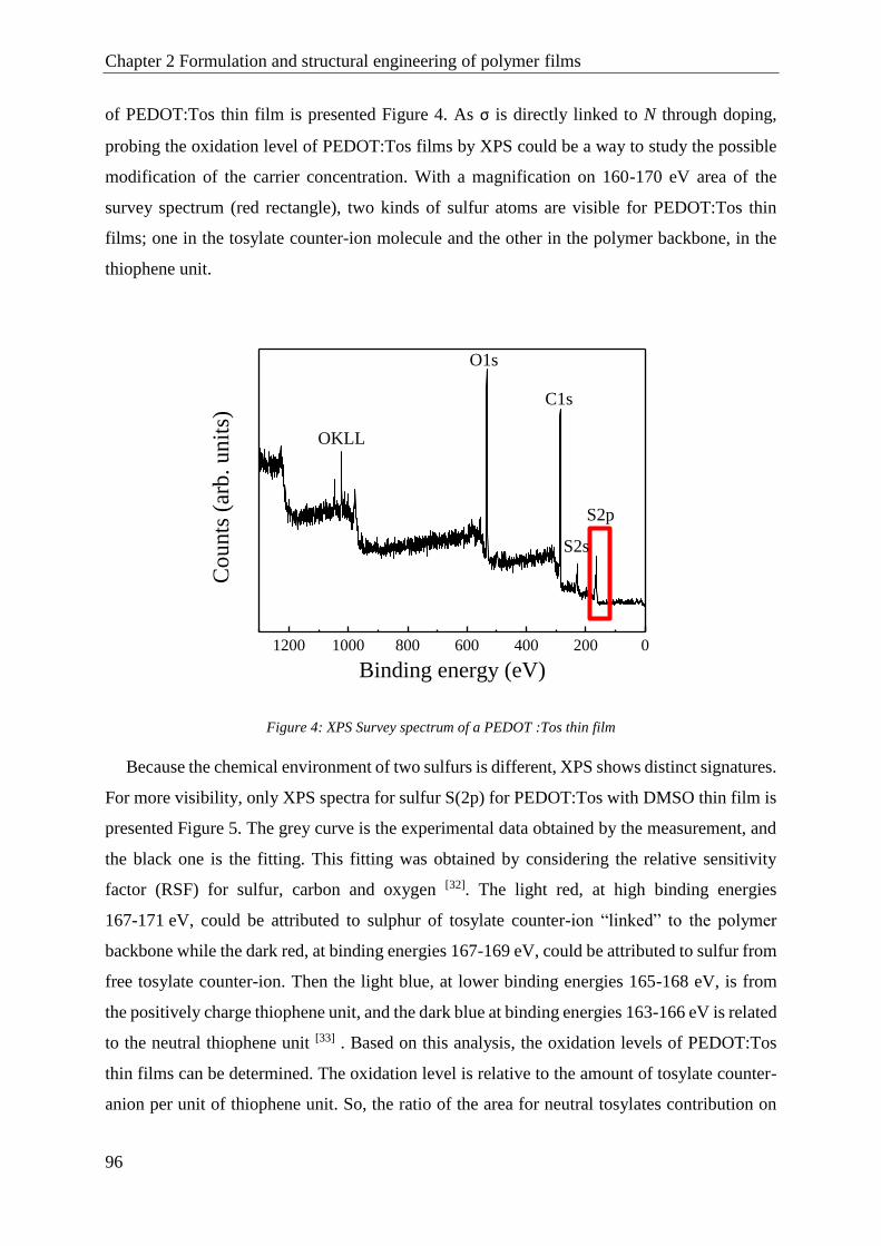
Chapter 2 Formulation and structural engineering of polymer films
96
of PEDOT:Tos thin film is presented Figure 4. As σ is directly linked to N through doping,
probing the oxidation level of PEDOT:Tos films by XPS could be a way to study the possible
modification of the carrier concentration. With a magnification on 160-170 eV area of the
survey spectrum (red rectangle), two kinds of sulfur atoms are visible for PEDOT:Tos thin
films; one in the tosylate counter-ion molecule and the other in the polymer backbone, in the
thiophene unit.
1200 1000 800 600 400 200 0
Co
un
ts (
arb.
un
its)
Binding energy (eV)
Figure 4: XPS Survey spectrum of a PEDOT :Tos thin film
Because the chemical environment of two sulfurs is different, XPS shows distinct signatures.
For more visibility, only XPS spectra for sulfur S(2p) for PEDOT:Tos with DMSO thin film is
presented Figure 5. The grey curve is the experimental data obtained by the measurement, and
the black one is the fitting. This fitting was obtained by considering the relative sensitivity
factor (RSF) for sulfur, carbon and oxygen [32]. The light red, at high binding energies
167-171 eV, could be attributed to sulphur of tosylate counter-ion “linked” to the polymer
backbone while the dark red, at binding energies 167-169 eV, could be attributed to sulfur from
free tosylate counter-ion. Then the light blue, at lower binding energies 165-168 eV, is from
the positively charge thiophene unit, and the dark blue at binding energies 163-166 eV is related
to the neutral thiophene unit [33] . Based on this analysis, the oxidation levels of PEDOT:Tos
thin films can be determined. The oxidation level is relative to the amount of tosylate counter-
anion per unit of thiophene unit. So, the ratio of the area for neutral tosylates contribution on
O1s
C1s
S2p
S2s
OKLL
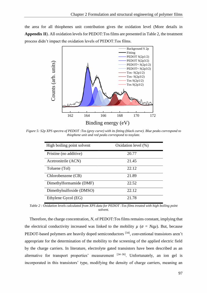
Chapter 2 Formulation and structural engineering of polymer films
97
the area for all thiophenes unit contribution gives the oxidation level (More details in
Appendix II). All oxidation levels for PEDOT:Tos films are presented in Table 2, the treatment
process didn’t impact the oxidation levels of PEDOT:Tos films.
Figure 5: S2p XPS spectra of PEDOT :Tos (grey curve) with its fitting (black curve). Blue peaks correspond to
thiophene unit and red peaks correspond to tosylate.
High boiling point solvent Oxidation level (%)
Pristine (no additive) 20.77
Acetronitrile (ACN) 21.45
Toluene (Tol) 22.12
Chlorobenzene (CB) 21.89
Dimethylformamide (DMF) 22.52
Dimethylsulfoxide (DMSO) 22.12
Ethylene Gycol (EG) 21.78
Table 2 : Oxidation levels calculated from XPS data for PEDOT :Tos films treated with high boiling point
solvent.
Therefore, the charge concentration, N, of PEDOT:Tos films remains constant, implying that
the electrical conductivity increased was linked to the mobility µ (σ = Nqµ). But, because
PEDOT-based polymers are heavily doped semiconductors [34], conventional transistors aren’t
appropriate for the determination of the mobility to the screening of the applied electric field
by the charge carriers. In literature, electrolyte gated transistors have been described as an
alternative for transport properties’ measurement [34–36]. Unfortunately, an ion gel is
incorporated in this transistors’ type, modifying the density of charge carriers, meaning an
162 164 166 168 170 172
Background S 2p
Fitting
PEDOT S(2p1/2)
PEDOT S(2p3/2)
PEDOT+ S(2p1/2)
PEDOT+ S(2p3/2)
Tos- S(2p1/2)
Tos- S(2p3/2)
Tos S(2p1/2)
Tos S(2p3/2)
Co
un
ts (
arb.
un
its)
Binding energy (eV)

Chapter 2 Formulation and structural engineering of polymer films
98
under-estimation of field effects and so mobility. Another way to indirectly observe an increase
in mobility could be to look at the morphology and more particularly the degree of
crystallization of pristine and solvent treated PEDOT:Tos samples. In fact, in organic
semiconductors, transport properties are strongly related to their film morphology [22,23,25,37–39].
Thanks to Grazing Incidence Wide Angle X-ray Scattering (GIWAXS), the structural
properties of the PEDOT:Tos thin films were probe to correlate the nature of the additive on
the conductivity, by an increase of the mobility. The (qr, qz) 2D scattering pattern recorded for
the pristine PEDOT:Tos film as well as those recorded for the acetonitrile-treated and DMSO-
treated films are presented in Figure 6 (a). Only three samples are presented to have easier
clarity on the graph. These films scatter anisotropically, with the majority of scattered intensity
along the near out-of-plane axis (qr = 0), so perpendicularly to the substrate. In Figure 6 (b), the
radially averaged scattered intensity is plotted with respect to the scattering vector q. In all
cases, the scattered intensity is presented after normalization for film thickness and background
subtraction, to allow for quantitative comparison between samples. Based on work of
Aasmundtveit et al., the strong peak at 0.44 Å-1 and 0.88 Å-1 are attributed on the (100) and (200)
reflections for all the PEDOT:Tos thin films [40]. The third peak observed at 1.3 Å-1 can be
assigned to the (300) reflection. The very low intensity of this peak means a limited long-range
order along this axis, indicating a material with paracrystalline distortions. Finally, at 1.77 Å-1
a broad and intense peak, the (020) reflection can be assigned as the π-π stacking direction [40].
On top of that, when the PEDOT:Tos thin films were treated by the high boiling point
solvent, an increase of the scattered intensity for the (100) and (020) peaks could be observed.
Furthermore, the area below the scattering peaks is directly correlated with the degree of
crystallinity, so adding a high boiling point solvent in the film increases its crystallinity and so
its mobility (increase of the conductivity without N modification). The increase of crystallinity
is due to a slower evaporation rate of the main solvent, 1-butanol (Tb = 115°C), when Tb of the
additive is higher, delaying the crystallization kinetics of the polymer chains and allowing
further crystallization. Many works in the literature confirmed this behaviour for conducting
polymers [21,34].
Then the anisotropic nature of the 2D images were examined, the in-plane and near out-of-
plane line-cuts are presented in Figure 6 (c) and (d). In the near out-of-plane pattern (I(qz) vs
qz, Figure 6 (d)), the (h00) group and the (020) reflection, similarly to the I(q) vs q pattern,
while in the in-plane pattern (I(qy) vs qy, Figure 6 (c)) the (h00) reflections are absent and only
the broad (020) reflection at 1.77 Å-1 is observed. In the in-plane pattern, the absence of the

Chapter 2 Formulation and structural engineering of polymer films
99
(h00) group can be interpreted by a preferential orientation of the crystallites in the film with
respect to the substrate. PEDOT chains are oriented in an edge-on configuration, where the
thiophene ring are aligned with their planes normal to the substrate. Nevertheless, the (020)
peak corresponding to the π-π stacking is also present, some crystallites are oriented with
face-on, with the thiophene ring parallel to the film plate.
In case of crystalline semiconducting polymers, chain & crystallite orientation and thin film
crystallinity have an important influence on the charge transport properties [12,25,34,38,41]. For
PEDOT, where the most efficient charge transport occurs by hopping between doped
conjugated chains [41], charge transport is anisotropic, and is dictate by the presence of highly
conducting crystallites “metallic” islands embedded in amorphous polymer matrix (less
conductive) [42]. Higher crystallinity can exhibit higher mobility and so electrical conductivity,
only if a majority of the crystallites orientation is edge-on orientation, thus inter-chain and intra-
chain hopping transport are promoted. This methodology developed in our laboratory, enhanced
charge transport improves thermoelectric properties by increasing the electrical conductivity
from 230 S/cm (pristine) to 635 S/cm (DMSO, best additive) to obtain the power factor of
69.2 µW.mK² for PEDOT:Tos thin films treated with DMSO [30].
0,0 0,5 1,0 1,5 2,0 2,50
50
100
150
Norm
ali
zed
In
ten
sity
(a.u
.)
020300
200
qz (Å
-1)
Pristine
Acetonitrile
DMSO
100
0,0 0,5 1,0 1,5 2,0 2,5
50
100
150
Norm
ali
zed
In
ten
sity
(a.u
.) Pristine
Acetonitrile
DMSO
qy (Å
-1)
020
0,0 0,5 1,0 1,5 2,0 2,50
2
4
Pristine
Acetonitrile
DMSO
Norm
ali
zed
In
ten
sity
(a.u
.)
200
020300
q (Å-1)
100
Figure 6: GIWAXS characterization of PEDOT :Tos films with additives.
(a) 2D GIWAXS images of PEDOT:Tos films.
The corresponding 1D scattering patterns: (b) radially average intensity with respect to the scattering vector q,
(c) the in-plane intensity line-cut and (d) the near out-of-plane intensity line-cut. The scattering intensity was
normalized by film thickness (substrate scattering was substracted).
(a) (b) (c) (d)
Pristine Acetonitrile DMSO (a)

Chapter 2 Formulation and structural engineering of polymer films
100
1.2 Thermoelectric properties enhancement by formulation
with an organic base, pyridine
Thermoelectric properties of PEDOT:Tos thin films could be tuned by tuning the
crystallisation degree via structural engineering. PEDOT:Tos thin films were prepared by
following the reaction procedure described in Appendix II [43,44]. The reaction is a thermally
activated in-situ solution oxidative polymerization of EDOT monomers in presence of
Fe(Tos)3. The polymerization prepared by in-situ polymerization techniques, using oxidants
based on Fe3+ derivate, are highly acidic and reactive, making the polymerization uncontrollable
and resulting in many structural defects in the thin film. With the addition of an organic base to
the PEDOT:Fe(Tos)3 formulation, the polymerization process can be slow down in order to
obtain higher molecular mass polymer chains [28,43–45]. This organic base will play the role of
an inhibitor, by increasing the pH in order to control the reaction rate. Based on previous work
in our laboratory, the organic base chosen is pyridine. To follow the polymerization kinetics,
UV-visible spectroscopy in formulations with and without pyridine was done. Similar
absorbance curves shape, with only absorbance intensity difference, due to a thickness
difference, were obtained (Figure 7).
400 600 800 1000 1200 1400 1600 18000.00
0.25
0.50
0.75
Prisitne
PEDOT + Pyridine
Ab
sorb
ance
(a.
u.)
Wavelength (nm)
Figure 7: UV-visible spectra of pristine and pyridine treated PEDOT:Tos “solutions”.
The influence of the pyridine on the kinetics is observable thanks to the absorbance at
1600 nm, corresponding to the bipolaron signature and is plotted Figure 8.
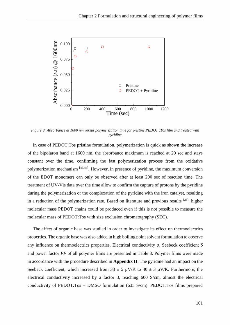
Chapter 2 Formulation and structural engineering of polymer films
101
0 200 400 600 800 1000 12000.000
0.025
0.050
0.075
0.100
Pristine
PEDOT + Pyridine
Ab
sorb
ance
(a.
u)
@ 1
60
0n
m
Time (sec)
Figure 8: Absorbance at 1600 nm versus polymerization time for pristine PEDOT :Tos film and treated with
pyridine
In case of PEDOT:Tos pristine formulation, polymerization is quick as shown the increase
of the bipolaron band at 1600 nm, the absorbance maximum is reached at 20 sec and stays
constant over the time, confirming the fast polymerization process from the oxidative
polymerization mechanism [43,44]. However, in presence of pyridine, the maximum conversion
of the EDOT monomers can only be observed after at least 200 sec of reaction time. The
treatment of UV-Vis data over the time allow to confirm the capture of protons by the pyridine
during the polymerization or the complexation of the pyridine with the iron catalyst, resulting
in a reduction of the polymerization rate. Based on literature and previous results [28], higher
molecular mass PEDOT chains could be produced even if this is not possible to measure the
molecular mass of PEDOT:Tos with size exclusion chromatography (SEC).
The effect of organic base was studied in order to investigate its effect on thermoelectrics
properties. The organic base was also added in high boiling point solvent formulation to observe
any influence on thermoelectrics properties. Electrical conductivity σ, Seebeck coefficient S
and power factor PF of all polymer films are presented in Table 3. Polymer films were made
in accordance with the procedure described in Appendix II. The pyridine had an impact on the
Seebeck coefficient, which increased from 33 ± 5 µV/K to 40 ± 3 µV/K. Furthermore, the
electrical conductivity increased by a factor 3, reaching 600 S/cm, almost the electrical
conductivity of PEDOT:Tos + DMSO formulation (635 S/cm). PEDOT:Tos films prepared

Chapter 2 Formulation and structural engineering of polymer films
102
with pyridine formulation also shown an overall 4-fold increase of the Power factor to achieve
96 µW/m.K² (Figure 9).
In the previous part, the introduction of high boiling point solvent allows an overall increase
of crystallinity as well as an improvement of the thermoelectric properties for PEDOT:Tos
films, the follow-up consists to make same formulations with high boiling point solvent and
pyridine to optimize thermoelectric properties [15]. A synergy effect could be observed when
the boiling point of the additive is higher than the boiling point of 1-butanol (Tb = 115°C), the
main solvent. This synergy could be observed as both the electrical conductivity and the
High boiling point solvent Tb (°C) S (µV/K) σ (S/cm) PF (µW/m.K²)
Pristine (no additive) - 33 ± 5 230 ± 11 25.0
Pyridine - 40 ± 3 600 ± 20 96
ACN + pyridine 82 41 ± 2 609 ± 11 102.4
Tol + pyridine 110 42 ± 4 615 ± 9 108.5
CB + pyridine 137 41 ± 4 1120 ± 8 188.3
DMF + pyridine 153 39 ± 3 1054 ± 16 160.3
DMSO + pyridine 189 44 ± 3 1240 ± 12 240.1
EG + pyridine 197 40 ± 5 1045 ± 10 167.2
Table 3 : Thermoelectric properties of the corresponding PEDOT :Tos films with high boiling point solvent and
pyridine.
80 120 160 200
0
500
1000
1500
Ele
ctri
cal
condcu
tivit
y (
S/c
m)
S
Tb (°C)
0
25
50
75
100 Seeb
eck co
efficient (µ
V/K
)
0
100
200
300
Pow
er Facto
r (µW
/mK
²)
Figure 9: Seebeck coefficient, electrical conductivity and power factor of PEDOT:Tos thin films treated with
high boiling point solvent and pyridine.
σ
S²σ
Chapter 2 Formulation and structural engineering of polymer films
103
Seebeck coefficient increase compare to PEDOT:Tos pristine films, from σ = 230
to σ = 1240 S/cm and from S = 33 to S = 44 µV/K, resulting to a Power factor of 240.1 µW/m.K²
(without modification of the oxidation level). As previously (Part on high boiling point solvent),
XPS spectroscopy was used to determine and compare the oxidation level of PEDOT:Tos
samples without additive, with pyridine and pyridine + high boiling point solvent (Table 4).
High boiling point solvent Oxidation level (%)
Pristine (no additive) 20.77
Pyridine 21.55
ACN + pyridine 20.74
Tol + pyridine 21.19
CB + pyridine 21.54
DMF + pyridine 22.32
DMSO + pyridine 21.48
EG + pyridine 21.98
Table 4 : Oxidation levels calculated from XPS data for PEDOT :Tos films treated with high boiling point
solvent and pyridine.
Based on the results presented Table 4, treatment process didn’t impact the oxidation levels
of PEDOT:Tos films. Therefore, the charge concentration, N, of PEDOT:Tos films remains
constant, implying that the electrical conductivity increased was linked to the mobility
µ (σ = Nqµ).
In organic semiconductors, transport properties are strongly related to their film morphology.
In order to elucidate the structural origin of the increase of thermoelectric properties [15,23,46],
GIWAXS experiments were done. The 2D scattering patterns for the various films are presented
in Figure 10 (a) (corrected by incident photon flux, acquisition time of 30 sec and scattering
volume to allow direct comparison). As previously with PEDOT:Tos thin films treated with
high boiling point solvent, a clear anisotropy signature could be observed on the pyridine treated
films pattern. Besides, this is along the near out-of-plane qz axis that the majority of the scattered
intensity is placed, confirming the preferential orientation of the PEDOT crystallites,
perpendicular to the substrate (Figure 10 (c)) [40]. A large increase of the scattered intensity is
apparent for PEDOT thin films prepared with pyridine and pyridine + DMSO formulations.
The radially averaged scattered intensity profiles are plotted Figure 10 (b). Three reflections
corresponding to the (h00) peak family (qh00 = 0.44, 0.88, 1.3 Å) and a (020) broader peak at
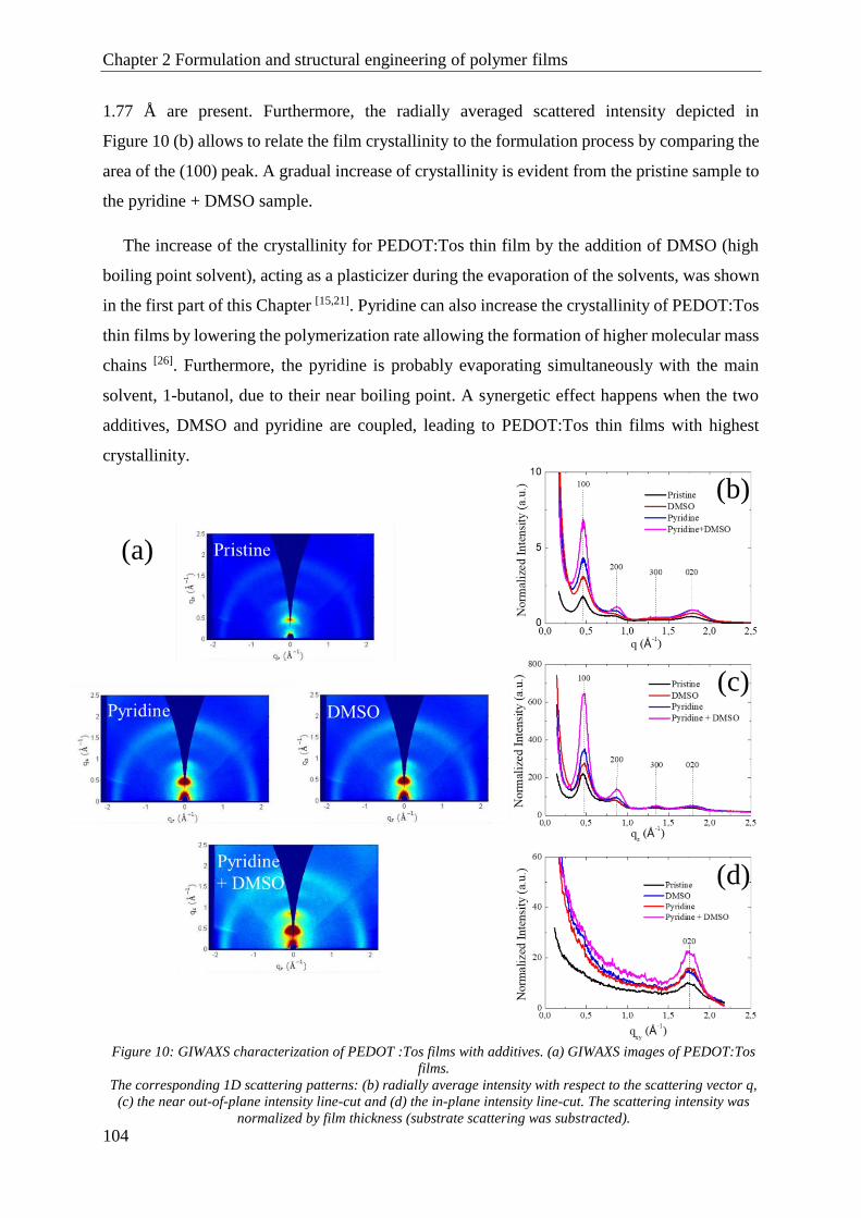
Chapter 2 Formulation and structural engineering of polymer films
104
1.77 Å are present. Furthermore, the radially averaged scattered intensity depicted in
Figure 10 (b) allows to relate the film crystallinity to the formulation process by comparing the
area of the (100) peak. A gradual increase of crystallinity is evident from the pristine sample to
the pyridine + DMSO sample.
The increase of the crystallinity for PEDOT:Tos thin film by the addition of DMSO (high
boiling point solvent), acting as a plasticizer during the evaporation of the solvents, was shown
in the first part of this Chapter [15,21]. Pyridine can also increase the crystallinity of PEDOT:Tos
thin films by lowering the polymerization rate allowing the formation of higher molecular mass
chains [26]. Furthermore, the pyridine is probably evaporating simultaneously with the main
solvent, 1-butanol, due to their near boiling point. A synergetic effect happens when the two
additives, DMSO and pyridine are coupled, leading to PEDOT:Tos thin films with highest
crystallinity.
(a)
(b)
(c)
(d)
Figure 10: GIWAXS characterization of PEDOT :Tos films with additives. (a) GIWAXS images of PEDOT:Tos
films.
The corresponding 1D scattering patterns: (b) radially average intensity with respect to the scattering vector q,
(c) the near out-of-plane intensity line-cut and (d) the in-plane intensity line-cut. The scattering intensity was
normalized by film thickness (substrate scattering was substracted).
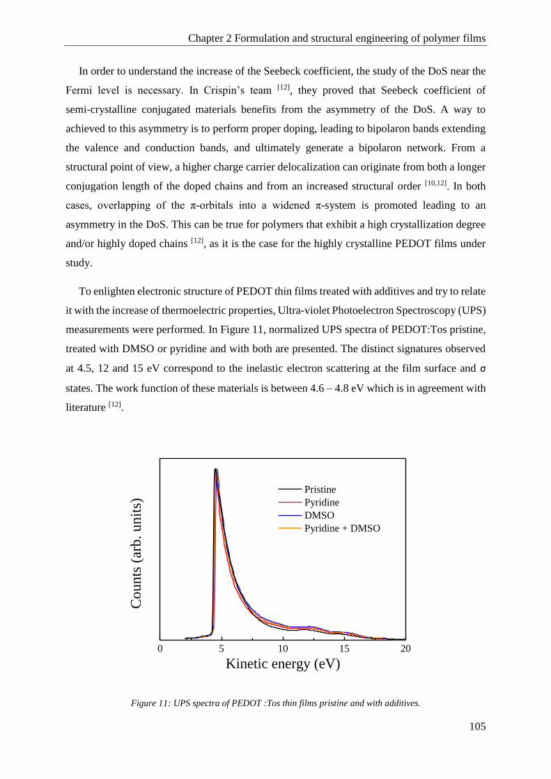
Chapter 2 Formulation and structural engineering of polymer films
105
In order to understand the increase of the Seebeck coefficient, the study of the DoS near the
Fermi level is necessary. In Crispin’s team [12], they proved that Seebeck coefficient of
semi-crystalline conjugated materials benefits from the asymmetry of the DoS. A way to
achieved to this asymmetry is to perform proper doping, leading to bipolaron bands extending
the valence and conduction bands, and ultimately generate a bipolaron network. From a
structural point of view, a higher charge carrier delocalization can originate from both a longer
conjugation length of the doped chains and from an increased structural order [10,12]. In both
cases, overlapping of the π-orbitals into a widened π-system is promoted leading to an
asymmetry in the DoS. This can be true for polymers that exhibit a high crystallization degree
and/or highly doped chains [12], as it is the case for the highly crystalline PEDOT films under
study.
To enlighten electronic structure of PEDOT thin films treated with additives and try to relate
it with the increase of thermoelectric properties, Ultra-violet Photoelectron Spectroscopy (UPS)
measurements were performed. In Figure 11, normalized UPS spectra of PEDOT:Tos pristine,
treated with DMSO or pyridine and with both are presented. The distinct signatures observed
at 4.5, 12 and 15 eV correspond to the inelastic electron scattering at the film surface and σ
states. The work function of these materials is between 4.6 – 4.8 eV which is in agreement with
literature [12].
0 5 10 15 20
Co
un
ts (
arb
. u
nit
s)
Kinetic energy (eV)
Pristine
Pyridine
DMSO
Pyridine + DMSO
Figure 11: UPS spectra of PEDOT :Tos thin films pristine and with additives.

Chapter 2 Formulation and structural engineering of polymer films
106
Figure 12 shows a magnified view at the higher kinetic energies (lower binding energies), at
which the band edge corresponding to deeper π-orbitals is localized. A broadening of the band
edge is evident for the PEDOT:Tos DMSO + Pyridine sample (orange curve) which is related
to a higher delocalization of the charge carriers in these deeper π-orbitals [47,48]. A similar
broadening should extend to all π-bands (including the ones near the Fermi position) which
would result in a more asymmetric DoS at the Fermi level. This is further translated into an
increase of the Seebeck coefficient for the PEDOT:Tos DMSO + pyridine material (orange
curve) since the DoS slope is proportional to S through the Mott formula (purple arrow) [12].
This extended overlapping of the π orbitals retrieved from the UPS analysis and intrinsic of
the increased thin film crystallinity, is also beneficial for the electrical conductivity of the
polymer film [12]. In conducting polymers, the main charge transport mechanism is hopping
transport of the charge carriers between low-energy “metallic” islands inside the amorphous
polymer matrix [42]. From an electronic point of view, these areas can be considered as the
overlapping π orbitals of the crystalline doped conjugated chains [49]. Hence, the hopping of the
carriers along these regions is assisted by decreasing the structural disorder of the PEDOT:Tos
thin films. This macroscopically results in higher carrier mobility and thus higher σ, as observed
for the thin films treated with DMSO and pyridine (Table 3).
2.0 1.5 1.0 0.5 0.0 -0.5
Co
un
ts (
arb
. u
nit
s)
Binding energy (eV)
Pristine
Pyridine
DMSO
Pyridine + DMSO
Figure 12: Magnification to low binding energy region of UPS previous spectra.

Chapter 2 Formulation and structural engineering of polymer films
107
Thanks to a fine tuning of polymerization kinetics for PEDOT:Tos thin films with pyridine,
an enhancement of thermoelectrics properties was achieved, as attested by both a mild
increment of the Seebeck coefficient and a three-fold increase of the electrical conductivity.
Then by adding pyridine to DMSO formulations, resulting PEDOT:Tos thin films obtained a
high Power factor of 237 µW/m.K² inherent to an increased charge carrier mobility and a higher
degree of crystallinity, thanks to a synergistically effect. Origins of these effects have been
found by UPS to a band broadening near the Fermi level due to a more extended π-orbital
system and by GIWAXS to a confirmation of a higher degree of crystallinity. These discoveries
are consistent with the current understanding on the correlation between electronic and
structural properties. In fact, PEDOT:Tos thin films with the highest crystallinity exhibits as
well the most broadened band edge due to extended π-orbital overlapping, and thus, the higher
thermoelectric efficiency.
1.3 Aging control
Thermoelectric properties, Seebeck coefficient and electrical conductivity, were tested over
a long period of time in order to check the stability of PEDOT:Tos pyridine and DMSO
formulations and films. The formulations and films were made in accordance to procedure
described in Appendix II. Oxidant solutions were stored at 4°C and resulted films were stored
in a petri dish inside a clean room (temperature, 22°C, and moisture level, 50%, were quite
stable).
In Figure 13, Seebeck coefficient and electrical conductivity are plotted versus time and
correspond to stability of the oxidant formulation. Thermoelectric properties are remaining
unaltered at least one month (27 days), however after this month, electrical conductivity drops
from 1250 to 850 S/cm in one month. Seebeck coefficient decrease is less important. This
decrease could be from pyridine evaporation during swab, explaining that the electrical
conductivity value is almost equal to PEDOT:Tos films only treated with DMSO
(σ (pyridine/DMSO) = 850 S/cm and σ (DMSO) = 635 S/cm).

Chapter 2 Formulation and structural engineering of polymer films
108
0 10 20 30 40 50 600
20
40
60
Seebeck coefficient
Electrical conductivity
Time (day)
See
bec
k c
oef
fici
ent
(µV
/K)
0
250
500
750
1000
1250
Electrical co
nd
uctiv
ity (S
/cm)
Figure 13: Seebeck coefficient (black square) and electrical conductivity (red square) of PEDOT:Tos samples
from the same oxidant formulation versus time.
Then the stability over time of PEDOT:Tos thin film was evaluated though probing of
thermoelectric properties. The Figure 14 corresponds to thermoelectric properties for the same
PEDOT:Tos thin film treated with pyridine and DMSO. Electrical conductivity stays constant
for 150 days (5 months) then drops to 0 S/cm in one more month. The decrease of the Seebeck
coefficient is harder to spot due to its low value and standard deviation (Table 1 and Table 3).
The hypothesis formulate is related to macroscopic defect appearing after 5 months (cracks),
and degrading film order/crystallinity inducing a huge drop of electrical conductivity. This
degradation is probably due to evaporation of additive or solvent trap inside the polymer thin
film matrix or the interaction between the polymer thin film surface and moisture.

Chapter 2 Formulation and structural engineering of polymer films
109
0 50 100 150 2000
20
40
60
Seebeck coefficient
Electrical conductivity
0
250
500
750
1000
1250
Electrical co
nd
uctiv
ity (S
/cm)S
eeb
eck
co
effi
cien
t (µ
V/K
)
Time (day)
Figure 14: Seebeck coefficient (black square) and electrical conductivity (red square) of the same PEDOT:Tos
thin film versus time.

Chapter 2 Formulation and structural engineering of polymer films
110
P3HT
Poly-3-hexylthiophene (P3HT) is an alkylated derivate of polythiophene, P3HT is one of the
most studied conjugated polymers thanks to its excellent intrinsic properties such as a good
solubility, appropriate energy gap, doping reversibility and excellent electrical properties (high
exciton mobility along its backbone) [50]. P3HT solutions, with easy processability, are suitable
for a variety of solution processes such as spray-coating [51], roll-to-roll printing [52], inkjet
printing [53] and spin-coating [54]. Thus, P3HT has been very successfully introduced in
optoelectronic [55–59] and organic field effect transistors [60,61] , these days scientists try to explore
its properties for organic thermoelectric applications [62–65].
Intrinsic P3HT electrical conductivity at room temperature is low, 3.15 x 10⁻⁷ S/m [66],
researcher found several options to address this problem. Some common techniques are done
by varying experimental condition such as solvent nature, temperature, deposition methods, and
annealing conditions during film formation, order to control the structural properties and so
electrical/electronic properties [67–69]. Another method to increase electrical conductivity is to
use dopant molecule (molecular electron acceptors or donors) to mimic p- & n-doping of
inorganic systems [70]. Doping of P3HT could be achieved by number of methods, but the most
famous is by “chemical doping” with a molecule that has a high electron affinity (electron
acceptors) into the film as described in Chapter 1 [71–73].
Scientific community focus its interest in F4TCNQ as dopant for P3HT films. The nature of
the interaction between F4TCNQ and P3HT in solution phase and film has been invested
intensely these past years [74–78]. Indeed, solvent and dopant concentration have drastically
impact on P3HT solution and film properties, as proven by various studies [78]. Solvent plays
an important role on π-π stacking of polymer chains and dopant/P3HT solubility [79]. Then
dopant concentration affects directly the structural characteristics of P3HT films, Gao and coll.
shown that doping efficiency depends on the ability of P3HT to form aggregates in presence of
F4TCNQ [80].
Furthermore, processing method have also a high influence on P3HT/F4TCNQ film
properties, especially on electrical conductivity [81–83]. Recently, three main processes were
investigated, solution doping [81], sequential doping [84] and vapour phase doping [63]. For
solution doping, P3HT and F4TCNQ are mixed together and directly casted into a thin film. In
contrast, sequential doping is a two steps process, with cast of the neat P3HT thin film than
F4TCNQ is deposited on top from an orthogonal solvent. Sequentially doped films have been

Chapter 2 Formulation and structural engineering of polymer films
111
shown to have higher conductivity than that of solution doped samples at the same dopant
concentration [85,86]. Indeed, with a solution mixed doping, the microstructure of the film is more
disturbed than with sequential casting that allows tie-chains connecting crystalline domains
formed in neat P3HT to be retained leading to high conductivity. Furthermore, in solution
doping, more aggregates are formed during the charge transfer in solution, causing a different
morphology in the cast films with poorly connected domains, decreasing the electrical
conductivity. The main drawback of these processing methods are the post-treatment thermal
annealing that can decompose or remove the dopant from the films at elevated temperature.
One of the solution to this post-treatment is the vapour phase deposition, allowing the
infiltration of F4TCNQ in P3HT thin film at mild temperature without disturbing too much
P3HT morphology (crystallinity) [63]. Unfortunately, this process is difficult to adapt due to
generally a lack of experimental information (dopant quantity, container size, atmosphere
temperature, etc.) and adapted material to the laboratory.
In this work, thanks to rigorous state of the art, solution mixed and sequential doping were
adapted to obtain P3HT:F4TCNQ thin films. The influence of dopant concentration on
thermoelectric properties was studied in order to obtain P3HT thin film with the best power
factor. Finally, the doping process efficiency was followed by UV-visible-IR analysis and
correlated to the morphology thanks to AFM analysis.
2.1 Solution-mixed doping method
The effect of dopant concentration, F4TCNQ, on P3HT thin film, prepared via solution-
mixed doping method, was studied in order to investigate their effect on thermoelectric
properties. All thermoelectric properties are presented in Table 2. Polymers films were made in
accordance with the procedure described in Appendix II. F4TCNQ concentration had a
significant impact on electrical conductivity and Seebeck coefficient, an antagonist behaviour
between these both parameters was observed. The highest electrical conductivity was reached
for 20 mol% of F4TCNQ at 4.3 S/cm and the highest Seebeck coefficient for pristine P3HT at
1458 µV/K (Table 5). Evidently, the power factor, S²σ, followed a trend with a maximum at
2.48 µW/m.K² (Figure 15).

Chapter 2 Formulation and structural engineering of polymer films
112
F4TCNQ concentration (mol%) S (µV/K) σ (S/cm) PF (µW/m.K²)
P3HT pristine 1458 ±101 1 x10⁻⁶ 2.12 x10⁻⁴
P3HT + 10 mol% F4TCNQ 387 ±10 0.02 ±0.01 0.30
P3HT + 20 mol% F4TCNQ 76 ±3 4.3 ±0.2 2.48
P3HT + 30 mol% F4TCNQ 45 ±5 1.8 ±0.1 0.36
Table 5 : Thermoelectric properties of the P3HT :F4TCNQ with different F4TCNQ concentration.
0 10 20 30
1E-7
1E-5
1E-3
0.1
10
Ele
ctri
cal
con
du
ctiv
ity
(S
/cm
)
S
S²
F4TCNQ conc. (mol%)
0
400
800
1200
1600
Seeb
eck co
efficient (µ
V/K
)
0.0
0.5
1.0
1.5
2.0
2.5
Pow
er Facto
r (µW
/mK
²)
Figure 15: Seebeck coefficient, electrical conductivity and power factor of P3HT thin films doped with F4TCNQ
by solution –mixed doping method.
The doping efficiency was followed by UV-visible-NIR analysis in addition to
thermoelectric measurements. UV-visible is perfect for the characterization of doped film,
thanks to sub-gap absorptions from charge carrier species. In case of P3HT:F4TCNQ films, the
main charge carriers are singly-charged polarons, confirmed by Wang et al. and their fitting to
optical spectra [87]. Positive polarons give rise to two allowed sub-gap transition bands; in P3HT,
these transitions occur at about 826 nm and 2400 nm [88]. Furthermore, the F4TCNQ counter-
ion shows four distinctive absorption band at 413, 688, 751 and 855 nm. Figure 16 shows
UV-visible-IP spectra, normalized to 1 at the P3HT π-π* maximum absorption (560 nm), of all
films prepared using the solution-mixed doping method at doping levels between 0 and

Chapter 2 Formulation and structural engineering of polymer films
113
30 mol% F4TCNQ. With F4TCNQ mole ratio rising, absorption bands corresponding to the
F4TCNQ•- radical anion (413, 688, 751 and 855 nm) grew in. P3HT•-+ presence was confirmed
by an increase of absorption band at 826 nm and the appearance of the tail of 2400 nm
absorption polaron band. Additionally, hypsochromic shift (≈ 50nm) occurs for the absorption
band at 560 nm corresponding to the P3HT π-π* related to F4TCNQ’s action. These results are
consistent with literature [89].
400 600 800 1000 1200 1400 1600 18000.0
0.2
0.4
0.6
0.8
1.0
1.2
P3HT
P3HT + F4TCNQ 10% mol
P3HT + F4TCNQ 20% mol
P3HT + F4TCNQ 30% mol
No
rmal
ized
Ab
sorp
tio
n
Wavelength (nm)
Figure 16: UV-visible spectra of P3HT :F4TCNQ thin films (solution-mixed doping).
Then the film morphology was studied by atomic force microscopy (AFM). All images of
films doped using the solution-mixed method are presented Figure 17. As is clearly visible, this
method yields significantly rougher films, RMS roughness was calculated directly from images.
Furthermore, a phase aggregation is visible when F4TCNQ is added to P3HT film. These
structures are almost certainly phase-segregated F4TCNQ domains. The vast differences in film
roughness and the phase segregation are related to the difficulty of processing for solution-
mixed doping method. Gao et al. proposed a mechanism by which doping could cause
aggregation [80]. They noticed an increase in J-aggregate which are indicative of significantly
increased polymer backbone rigidity thanks to resonance Raman studies of doped films.
Implying the F4TCNQ primarily injects holes into aggregated P3HT domains, and resulting of
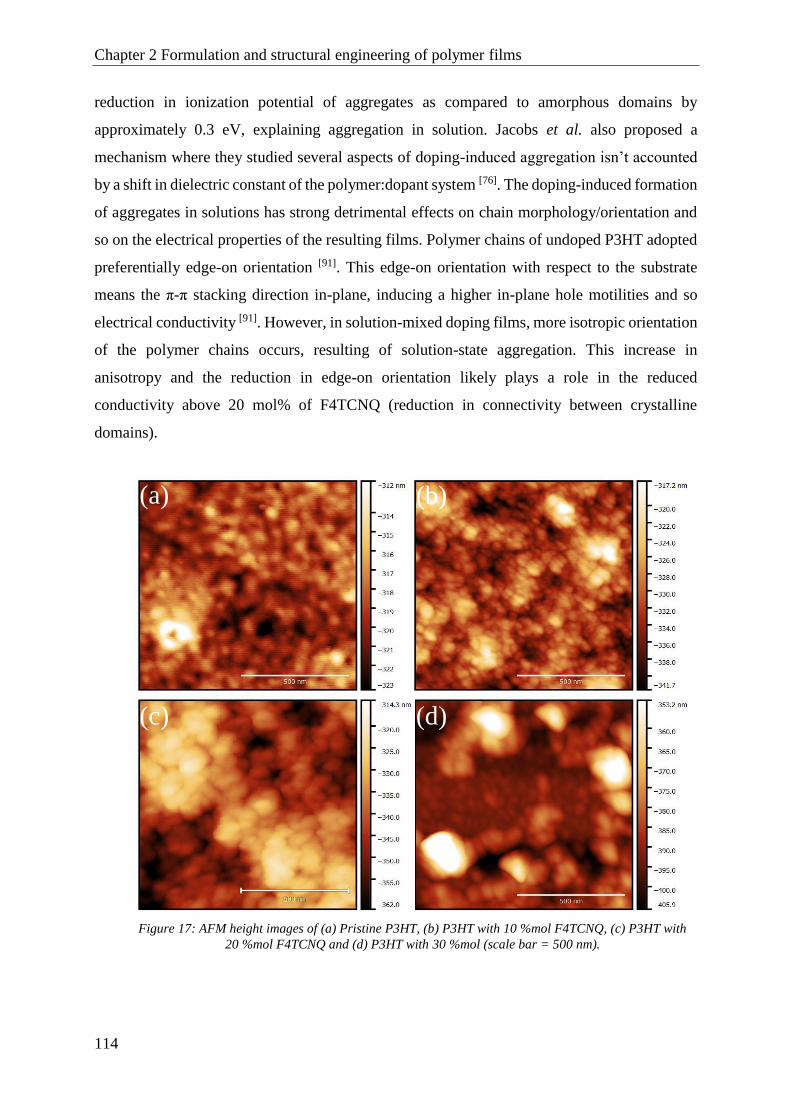
Chapter 2 Formulation and structural engineering of polymer films
114
reduction in ionization potential of aggregates as compared to amorphous domains by
approximately 0.3 eV, explaining aggregation in solution. Jacobs et al. also proposed a
mechanism where they studied several aspects of doping-induced aggregation isn’t accounted
by a shift in dielectric constant of the polymer:dopant system [76]. The doping-induced formation
of aggregates in solutions has strong detrimental effects on chain morphology/orientation and
so on the electrical properties of the resulting films. Polymer chains of undoped P3HT adopted
preferentially edge-on orientation [91]. This edge-on orientation with respect to the substrate
means the π-π stacking direction in-plane, inducing a higher in-plane hole motilities and so
electrical conductivity [91]. However, in solution-mixed doping films, more isotropic orientation
of the polymer chains occurs, resulting of solution-state aggregation. This increase in
anisotropy and the reduction in edge-on orientation likely plays a role in the reduced
conductivity above 20 mol% of F4TCNQ (reduction in connectivity between crystalline
domains).
(a) (b)
(c) (d)
Figure 17: AFM height images of (a) Pristine P3HT, (b) P3HT with 10 %mol F4TCNQ, (c) P3HT with
20 %mol F4TCNQ and (d) P3HT with 30 %mol (scale bar = 500 nm).
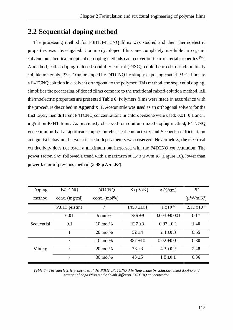
Chapter 2 Formulation and structural engineering of polymer films
115
2.2 Sequential doping method
The processing method for P3HT:F4TCNQ films was studied and their thermoelectric
properties was investigated. Commonly, doped films are completely insoluble in organic
solvent, but chemical or optical de-doping methods can recover intrinsic material properties [92].
A method, called doping-induced solubility control (DISC), could be used to stack mutually
soluble materials. P3HT can be doped by F4TCNQ by simply exposing coated P3HT films to
a F4TCNQ solution in a solvent orthogonal to the polymer. This method, the sequential doping,
simplifies the processing of doped films compare to the traditional mixed-solution method. All
thermoelectric properties are presented Table 6. Polymers films were made in accordance with
the procedure described in Appendix II. Acetonitrile was used as an orthogonal solvent for the
first layer, then different F4TCNQ concentrations in chlorobenzene were used: 0.01, 0.1 and 1
mg/ml on P3HT films. As previously observed for solution-mixed doping method, F4TCNQ
concentration had a significant impact on electrical conductivity and Seebeck coefficient, an
antagonist behaviour between these both parameters was observed. Nevertheless, the electrical
conductivity does not reach a maximum but increased with the F4TCNQ concentration. The
power factor, S²σ, followed a trend with a maximum at 1.48 µW/m.K² (Figure 18), lower than
power factor of previous method (2.48 µW/m.K²).
Doping
method
F4TCNQ
conc. (mg/ml)
F4TCNQ
conc. (mol%)
S (µV/K) σ (S/cm) PF
(µW/m.K²)
P3HT pristine / 1458 ±101 1 x10⁻⁶ 2.12 x10⁻⁴
Sequential
0.01 5 mol% 756 ±9 0.003 ±0.001 0.17
0.1 10 mol% 127 ±3 0.87 ±0.1 1.40
1 20 mol% 52 ±4 2.4 ±0.3 0.65
Mixing
/ 10 mol% 387 ±10 0.02 ±0.01 0.30
/ 20 mol% 76 ±3 4.3 ±0.2 2.48
/ 30 mol% 45 ±5 1.8 ±0.1 0.36
Table 6 : Thermoelectric properties of the P3HT :F4TCNQ thin films made by solution-mixed doping and
sequential deposition method with different F4TCNQ concentration

Chapter 2 Formulation and structural engineering of polymer films
116
0.01 0.1 1
1E-7
1E-5
1E-3
0.1
10
Ele
ctri
cal
con
du
ctiv
ity
(S
/cm
)
S
S²
F4TCNQ solution conc. (mg/ml)
0
200
400
600
800
1000
1200
1400
1600
Seeb
eck co
efficient (µ
V/K
)
0.0
0.5
1.0
1.5
Pow
er F
acto
r (µW
/mK²)
Figure 18: Seebeck coefficient, electrical conductivity and power factor of P3HT thin films doped with F4TCNQ
by sequential method.
As previously, the doping efficiency was followed by UV-visible-IR analysis. Figure 19
shows UV-visible-IR spectra of all P3HT films prepared, light color and dark color are
corresponding to solution-mixed doping method and sequential processing method
respectively. All spectra are normalized to 1 at the P3HT π-π* maximum absorption (560 nm).
Characteristic peaks of P3HT doped by F4TCNQ are visible for sequential processing doping
(413, 688, 751, 826, 855 and tail of 2400 nm) confirming the availability of this method. By
comparing the intensity of these characteristic peaks, an approximate doping level could be
determined for sequential processing method (Table 6).

Chapter 2 Formulation and structural engineering of polymer films
117
400 600 800 1000 1200 1400 1600 18000.0
0.2
0.4
0.6
0.8
1.0
1.2 P3HT
P3HT + F4TCNQ 10 mol%
P3HT + F4TCNQ 20 mol%
P3HT + F4TCNQ 30 mol%
P3HT + F4TCNQ 0.01 mg/ml
P3HT + F4TCNQ 0.1 mg/ml
P3HT + F4TCNQ 1 mg/ml
Norm
aliz
ed A
bso
rpti
on
Wavelength (nm)
Figure 19: Comparison of UV-visible spectra for P3HT :F4TCNQ thin films made by solution-mixed doping and
sequential process.
Comparable doping level were obtained with these two different methods and almost the
same thermoelectric properties were achieved, Figure 20 allows to compare these methods in
function of F4TCNQ molar concentration. As described previously, electrical properties of
films are related to the doping-induced formation of nanoparticles in solution, sequential doping
method overcomes this issue. In their work, Jacobs et al. clearly established that P3HT films
are insoluble after sequential doping from a F4TCNQ/acetonitrile solution [92]. Despite this
insolubility, these films have shown a solvatochromic absorption shift in good solvents for
P3HT (i.e. chlorobenzene), indicating that solvents were able to infiltrate crystallites in the film
without causing dissolution.

Chapter 2 Formulation and structural engineering of polymer films
118
0 10 20 30 40
1E-7
1E-5
1E-3
0.1
10
Ele
ctri
cal
con
du
ctiv
ity
(S
/cm
)
(seq.)
S (seq.)
(mixed)
S (mixed)
F4TCNQ conc. (mol%)
0
200
400
600
800 S
eebeck
coefficien
t (µV
/K)
Figure 20: Comparison of Seebeck coefficient and electrical conductivity of P3HT:F4TCNQ thin films doped by
solution-mixed doping (full colour symbols) and sequential process (empty colour symbols).
In order to understand this phenomenon, atomic force microscopy (AFM) was used. All
images of films doped using both the solution-mixed and sequential method are presented
Figure 21. Unlike the mixed-solution films which have high roughness and phase segregation,
the films for the sequential process show the same morphology and have a lower roughness.
Furthermore, no significant phase segregation is visible in these films, very probably F4TCNQ
does not infiltrate P3HT crystallites but intercalate into P3HT crystallites. These results confirm
that doping from acetonitrile solution does not affect P3HT crystallinity and allows to obtain
an increase of electrical conductivity.

Chapter 2 Formulation and structural engineering of polymer films
119
Figure 21: Comparison of AFM height images for solution-mixed (b, c, d) and sequential (e, f, g) doping process.
(a) Pristine P3HT, (b) 10 %mol F4TCNQ, (c) 20 %mol F4TCNQ, (d) 30 %mol F4TCNQ,
(e) 5 %mol F4TCNQ, (f) 10 %mol F4TCNQ and (g) 20 %mol F4TCNQ (scale bar = 500 nm).
(a)
(b) (c) (d)
(e) (f) (g)
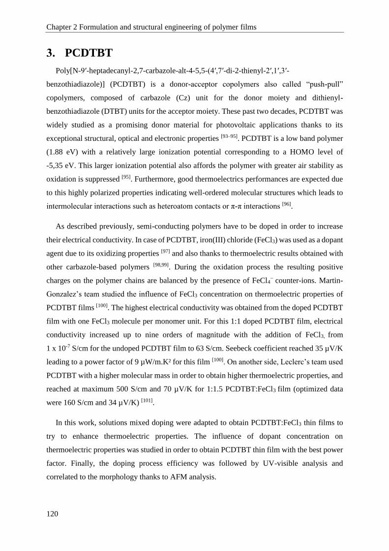
Chapter 2 Formulation and structural engineering of polymer films
120
PCDTBT
Poly[N-9′-heptadecanyl-2,7-carbazole-alt-4-5,5-(4′,7′-di-2-thienyl-2′,1′,3′-
benzothiadiazole)] (PCDTBT) is a donor-acceptor copolymers also called “push-pull”
copolymers, composed of carbazole (Cz) unit for the donor moiety and dithienyl-
benzothiadiazole (DTBT) units for the acceptor moiety. These past two decades, PCDTBT was
widely studied as a promising donor material for photovoltaic applications thanks to its
exceptional structural, optical and electronic properties [93–95]. PCDTBT is a low band polymer
(1.88 eV) with a relatively large ionization potential corresponding to a HOMO level of
-5,35 eV. This larger ionization potential also affords the polymer with greater air stability as
oxidation is suppressed [95]. Furthermore, good thermoelectrics performances are expected due
to this highly polarized properties indicating well-ordered molecular structures which leads to
intermolecular interactions such as heteroatom contacts or π-π interactions [96].
As described previously, semi-conducting polymers have to be doped in order to increase
their electrical conductivity. In case of PCDTBT, iron(III) chloride (FeCl3) was used as a dopant
agent due to its oxidizing properties [97] and also thanks to thermoelectric results obtained with
other carbazole-based polymers [98,99]. During the oxidation process the resulting positive
charges on the polymer chains are balanced by the presence of FeCl4− counter-ions. Martin-
Gonzalez’s team studied the influence of FeCl3 concentration on thermoelectric properties of
PCDTBT films [100]. The highest electrical conductivity was obtained from the doped PCDTBT
film with one FeCl3 molecule per monomer unit. For this 1:1 doped PCDTBT film, electrical
conductivity increased up to nine orders of magnitude with the addition of FeCl3, from
1 x 10⁻⁷ S/cm for the undoped PCDTBT film to 63 S/cm. Seebeck coefficient reached 35 µV/K
leading to a power factor of 9 µW/m.K² for this film [100]. On another side, Leclerc’s team used
PCDTBT with a higher molecular mass in order to obtain higher thermoelectric properties, and
reached at maximum 500 S/cm and 70 µV/K for 1:1.5 PCDTBT:FeCl3 film (optimized data
were 160 S/cm and 34 µV/K) [101].
In this work, solutions mixed doping were adapted to obtain PCDTBT:FeCl3 thin films to
try to enhance thermoelectric properties. The influence of dopant concentration on
thermoelectric properties was studied in order to obtain PCDTBT thin film with the best power
factor. Finally, the doping process efficiency was followed by UV-visible analysis and
correlated to the morphology thanks to AFM analysis.
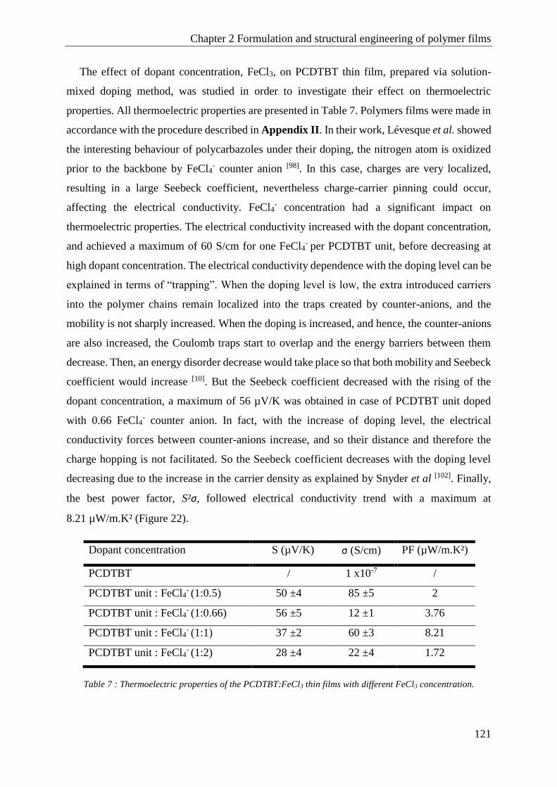
Chapter 2 Formulation and structural engineering of polymer films
121
The effect of dopant concentration, FeCl3, on PCDTBT thin film, prepared via solution-
mixed doping method, was studied in order to investigate their effect on thermoelectric
properties. All thermoelectric properties are presented in Table 7. Polymers films were made in
accordance with the procedure described in Appendix II. In their work, Lévesque et al. showed
the interesting behaviour of polycarbazoles under their doping, the nitrogen atom is oxidized
prior to the backbone by FeCl4- counter anion [98]. In this case, charges are very localized,
resulting in a large Seebeck coefficient, nevertheless charge-carrier pinning could occur,
affecting the electrical conductivity. FeCl4- concentration had a significant impact on
thermoelectric properties. The electrical conductivity increased with the dopant concentration,
and achieved a maximum of 60 S/cm for one FeCl4- per PCDTBT unit, before decreasing at
high dopant concentration. The electrical conductivity dependence with the doping level can be
explained in terms of “trapping”. When the doping level is low, the extra introduced carriers
into the polymer chains remain localized into the traps created by counter-anions, and the
mobility is not sharply increased. When the doping is increased, and hence, the counter-anions
are also increased, the Coulomb traps start to overlap and the energy barriers between them
decrease. Then, an energy disorder decrease would take place so that both mobility and Seebeck
coefficient would increase [10]. But the Seebeck coefficient decreased with the rising of the
dopant concentration, a maximum of 56 µV/K was obtained in case of PCDTBT unit doped
with 0.66 FeCl4- counter anion. In fact, with the increase of doping level, the electrical
conductivity forces between counter-anions increase, and so their distance and therefore the
charge hopping is not facilitated. So the Seebeck coefficient decreases with the doping level
decreasing due to the increase in the carrier density as explained by Snyder et al [102]. Finally,
the best power factor, S²σ, followed electrical conductivity trend with a maximum at
8.21 µW/m.K² (Figure 22).
Dopant concentration S (µV/K) σ (S/cm) PF (µW/m.K²)
PCDTBT / 1 x10⁻⁷ /
PCDTBT unit : FeCl4- (1:0.5) 50 ±4 85 ±5 2
PCDTBT unit : FeCl4- (1:0.66) 56 ±5 12 ±1 3.76
PCDTBT unit : FeCl4- (1:1) 37 ±2 60 ±3 8.21
PCDTBT unit : FeCl4- (1:2) 28 ±4 22 ±4 1.72
Table 7 : Thermoelectric properties of the PCDTBT:FeCl3 thin films with different FeCl3 concentration.

Chapter 2 Formulation and structural engineering of polymer films
122
0 0.5 0.6 1 2
0
10
20
30
40
50
60
70
80
Ele
ctri
cal
con
du
ctiv
ity
(S
/cm
)
S
S²
FeCl4
- per PCDTBT unit
0
20
40
60 S
eebeck
coefficien
t (µV
/K)
0
2
4
6
8
Pow
er F
acto
r (µW
/mK²)
Figure 22: Seebeck coefficient, electrical conductivity and power factor of PCDTBT thin films doped with FeCl3.
The doping efficiency was followed UV-visible-NIR analysis in addition to thermoelectric
measurements. UV-visible is perfect for the characterization of doped polymer films. The thin
film spectrum of the pristine PCDTBT consists of a peak at around 395 nm and a peak at around
550 nm, which could be attributed to carbazole and benzothiadiazole units respectively [98].
Doping results in a gradual bathochromic effect (red shift) of both absorption peak from 395 nm
and 550 nm for the pristine PCDTBT to 402 nm and 570 nm for PCDTBT doped with two
FeCl4- counter anions per PCDTBT unit (Figure 23, grey dots lines).
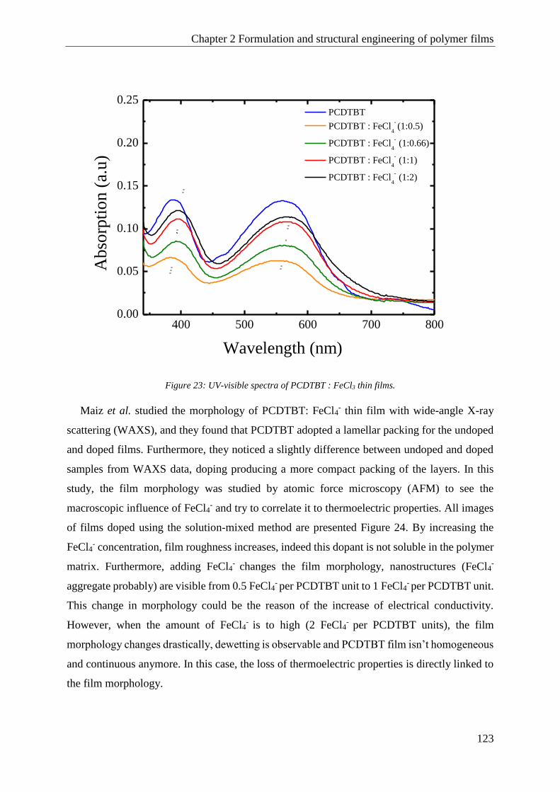
Chapter 2 Formulation and structural engineering of polymer films
123
400 500 600 700 8000.00
0.05
0.10
0.15
0.20
0.25 PCDTBT
PCDTBT : FeCl4
-
(1:0.5)
PCDTBT : FeCl4
-
(1:0.66)
PCDTBT : FeCl4
-
(1:1)
PCDTBT : FeCl4
-
(1:2)
Abso
rpti
on
(a.
u)
Wavelength (nm)
Figure 23: UV-visible spectra of PCDTBT : FeCl3 thin films.
Maiz et al. studied the morphology of PCDTBT: FeCl4- thin film with wide-angle X-ray
scattering (WAXS), and they found that PCDTBT adopted a lamellar packing for the undoped
and doped films. Furthermore, they noticed a slightly difference between undoped and doped
samples from WAXS data, doping producing a more compact packing of the layers. In this
study, the film morphology was studied by atomic force microscopy (AFM) to see the
macroscopic influence of FeCl4- and try to correlate it to thermoelectric properties. All images
of films doped using the solution-mixed method are presented Figure 24. By increasing the
FeCl4- concentration, film roughness increases, indeed this dopant is not soluble in the polymer
matrix. Furthermore, adding FeCl4- changes the film morphology, nanostructures (FeCl4
-
aggregate probably) are visible from 0.5 FeCl4- per PCDTBT unit to 1 FeCl4
- per PCDTBT unit.
This change in morphology could be the reason of the increase of electrical conductivity.
However, when the amount of FeCl4- is to high (2 FeCl4
- per PCDTBT units), the film
morphology changes drastically, dewetting is observable and PCDTBT film isn’t homogeneous
and continuous anymore. In this case, the loss of thermoelectric properties is directly linked to
the film morphology.

Chapter 2 Formulation and structural engineering of polymer films
124
Figure 24: AFM height images of (a) Pristine PCDTBT, (b) PCDTBT: FeCl3 (1:0.5), (c) PCDTBT: FeCl3 (1:0.66),
(d) PCDTBT: FeCl3 (1:1) and (e) PCDTBT: FeCl3 (1:2) thin films (scale bar = 500 nm).
(b) (c)
(d) (e)
(a)

Chapter 2 Formulation and structural engineering of polymer films
125
PTB7
Poly [[4,8-bis[(2-ethylhexyl)oxy]benzo[1,2-b:4,5-b']dithiophene-2,6-diyl][3-fluoro-2-[(2-
ethylhexyl)carbonyl]thieno[3,4-b]thiophenediyl]] (PTB7) is a polymer from the low bandgap
family, composed alternately of 3-fluorothieno- [3,4-b]thiophene-2-carboxylate (TT) and
benzo[1,2-b:4,5-b′]- dithiophene (BDT) moieties. PTB7 has shown very promising properties
[103–106] especially in organic field effect transistors field [107] and in photovoltaic application as
donor material leading to power conversion efficiency (PCE) as high as 9.2% [108,109]. This high
efficiency could be attributed to the large transition-state dipole moment μtr = 8.23 D, an
excited-state dipole moment μe = 7.13 D and a ground-state dipole moment μg = 3.76 D of the
thienothiophene (TT) monomer [110]. As a comparison, the dipole moment of the P3HT polymer
is in the range 1.0–1.6 D [111]. This large dipole moment value of PTB7 allows a better molecular
orientation under an external application of an electric field.
Rastegaralam et al. used PTB7 as active layer for thermoelectric applications by adapting a
strategy developed to increase the PCE in solar cells [112]. They studied the influence of a
structuring agent, 1,8-diiodooctane (DIO), in various high boiling point chlorinated solvent in
order to increase the polymer’s crystallinity expecting to increase the charge carrier mobility.
The electrical conductivity and Seebeck coefficient values are as follows: 0.5 S/m & 670 µV/K,
0.8 S/m & 702 µV/K, and 1.2 S/m & 726 µV/K for samples made of chlorobenzene (CB),
1,2-dichlorobenzene (DCB) and 1,2,4-trichlorobenzene (TCB) without DIO, respectively.
Then, by adding DIO, they only managed to increase electrical conductivity and Seebeck
coefficient for TCB from 1.2 S/m to 1.78 S/m and 726 µV/K to 758 µV/K. Thus, they managed
to increase the electrical conductivity and the Seebeck coefficient for higher boiling point
solvent TCB, leading a power factor of 1 µW/m.K².
Despite this low power factor value compared to PEDOT, P3HT or PCDTBT values
previously cited, the most interesting part is the high Seebeck coefficient obtained (around
700 µV/K) with proper electrical conductivity value (0.018 S/cm) comparable to Seebeck
coefficient of inorganic material like silicon (440 µV/K) [113].
In this work, the same procedure than P3HT: F4TCNQ and PCDTBT:FeCl3 thin films was
applied. The solution mixed doping procedure was applied to this polymer to try to enhance
thermoelectric properties. The influence of structural agent on thermoelectric properties was
studied in order to obtain PTB7 thin film with the best power factor. Finally, the increase of

Chapter 2 Formulation and structural engineering of polymer films
126
thermoelectric properties was followed by UV-visible analysis and correlated to the
morphology thanks to AFM analysis.
In this part, based on Rastegaralam et al. work, only the PTB7 in trichlorobenzene (TCB)
was used with DIO as structural agent [112]. The effect of DIO on PTB7 thin film, prepared via
solution-mixed method, was studied in order to obtain the best thermoelectric properties.
Polymers films were made in accordance with the procedure described in Appendix II. DIO
had a positive impact on thermoelectric properties, electrical conductivity and Seebeck
coefficient, thus a power factor of 0.9 µW/m.K² was obtained (Figure 25).
As shown by UV-visible analysis, no difference is noticeable between the pristine PTB7 and
the PTB7 with DIO (Figure 26). The difference in absorbance is due to a difference of thickness,
confirmed by a profilometer. This is well-known that DIO acts as a structural agent influencing
the nanostructured morphology [114]. So, to find an origin of both increase of electrical
conductivity and Seebeck coefficient, morphology study, by AFM, was conducted (Figure 27).
TCB TCB + DIO
0.000
0.005
0.010
0.015
0.020
Ele
ctri
cal
con
du
ctiv
ity
(S
/cm
)
TCB TCB + DIO
0
100
200
300
400
500
600
700
800
See
bec
k c
oef
fici
ent
(µV
/K)
TCB TCB + DIO
0.0
0.2
0.4
0.6
0.8
1.0
Pow
er F
acto
r (µ
W/m
K²)
Figure 25: Thermoelectric properties (Seebeck coefficient, electrical conductivity and power factor) of the
PTB7 and PTB7 + DIO thin films.

Chapter 2 Formulation and structural engineering of polymer films
127
400 500 600 700 800 900 10000.00
0.05
0.10
0.15
0.20
0.25
0.30A
bso
rpti
on
(a.
u.)
PTB7
PTB7+ DIO
Wavelength (nm)
Figure 26: UV-visible spectra of PTB7 and PTB7 + DIO thin film.
The neat PTB7 is homogeneous as expected for homopolymer films. When DIO is added to
the formulation, the film morphology changes and the root-mean-square (RMS) surface
roughness decreased from 4.9 to 0.51 nm. DIO with its high boiling point of 332.5°C should
allow PTB7 fibers to “move” more freely during the film formation, DIO inhibiting the
evaporation of the solvent. These results are consistent with the UV-visible (decrease of
thickness) and the increase of thermoelectric properties.
Figure 27: AFM height images of (a) Pristine PTB7 and (b) PTB7 with DIO (scale bar = 500 nm).
(a) (b)

Chapter 2 Formulation and structural engineering of polymer films
128
B n-type materials engineering
PCBM
Fullerenes family, such as PCBM and PC71BM, are the most commonly used acceptors in
optoelectronic field. Indeed, fullerenes were widely studied due to their excellent electron
transport properties, high electron affinity and their ability to form favorable nanoscale network
with donor molecules. However, fullerene derivatives also exhibit several non-trivial
drawbacks that hinder their use in practical applications. First, the relatively low lowest
unoccupied molecular orbital (LUMO) energy level (~4.1 to -4.3 eV). set a limitation [115].
Second, fullerene derivatives have strong tendency to crystallize and aggregate causing a
performance degradation in long term [116,117]. Finally, fullerenes are limited by their intrinsic
low electron mobility and electrical conductivity [118,119].
For thermoelectric application, fullerene derivatives (PCBM) stay among the best n-type
organic semi-conductors with high electron mobility and good thermal stability [120]. Bao’s
group developed an efficient and stable n-type dopant, N-DPBI, and thanks to a doping
solution-processed achieved 1.9 x10⁻³ S/cm for PCBM films [121]. Gao et al. developed an other
methods based on co-doping with N-DPBI and acridine orange base
(3,6-bis(dimethylaminoacridine) (AOB) resulting in PCBM films with high electrical
conductivity and Seebeck coefficient [122]. The doping mechanism of AOB was studied by Li et
al. [123] and proposed that during the process (co-evaporation), AOB and fullerene formed a
dyad of a positively charged acridine dye and a C60 anion radical connected by a C-N chemical
bond.
In this work, PC71BM was formulated with N-DPBI and AOB. The protocol was adapted
from a co-evaporation process to obtain a more suitable process for liquid deposition. The
thermoelectric properties (electrical conductivity and Seebeck coefficient) for different dopant
concentrations in PCBM films were evaluated and followed by UV-visible analysis
The influence of AOB, a heterogeneous guest, on PCBM:N-DPBI thin films, prepared via
an inverse-sequential doping, was studied in order to investigate its effect on thermoelectric
properties. All thermoelectric properties are presented in Table 8. Organic films were made in
accordance with the procedure described in Appendix II. Based on Kemerink and coll. work,
N-DPBI was used as dopant with a concentration of 5 wt% [124]. AOB concentration had a

Chapter 2 Formulation and structural engineering of polymer films
129
significant impact on thermoelectric properties. Despite, Seebeck coefficient decreases with the
increase of AOB amount, electrical conductivity followed a bell-shape trend with a maximum
at 0.7 S/cm which is a high value for n-type material (c.f. Chapter 1), leading to a power factor
of 11.88 µW/m.K² (Figure 28).
AOB conc. (mol%) S (µV/K) σ (S/cm) PF
(µW/m.K²)
0 -775 ±12 8.5x10⁻⁸ 5x10⁻⁶
5 mol% -554 ±11 0.05 ±0.01 1.53
10 mol% -412 ±10 0.7 ±0.1 11.88
20 mol% -332 ±11 0.22 ±0.1 2.44
30 mol% -239 ±15 1x10⁻³ 5.7x10⁻⁴
Table 8 : Thermoelectric properties of the PCBM:N-DPBI thin films with different AOB concentration
0 10 20 30
0.0
0.2
0.4
0.6
0.8
1.0
1.2
1.4
Ele
ctri
cal
con
du
ctiv
ity
(S
/cm
)
S
S²
AOB conc. (wt%)
-1000
-800
-600
-400
-200
Seeb
eck co
efficient (µ
V/K
)
0
2
4
6
8
10
12
14
16
Pow
er Facto
r (µW
/mK
²)
Figure 28: Seebeck coefficient, electrical conductivity and power factor of PCBM:N-DPBI thin films with
different AOB concentration.
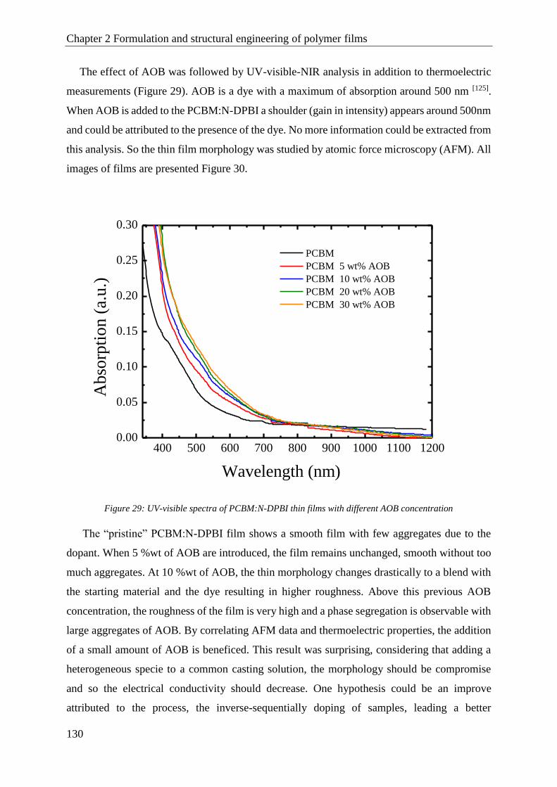
Chapter 2 Formulation and structural engineering of polymer films
130
The effect of AOB was followed by UV-visible-NIR analysis in addition to thermoelectric
measurements (Figure 29). AOB is a dye with a maximum of absorption around 500 nm [125].
When AOB is added to the PCBM:N-DPBI a shoulder (gain in intensity) appears around 500nm
and could be attributed to the presence of the dye. No more information could be extracted from
this analysis. So the thin film morphology was studied by atomic force microscopy (AFM). All
images of films are presented Figure 30.
400 500 600 700 800 900 1000 1100 12000.00
0.05
0.10
0.15
0.20
0.25
0.30
PCBM
PCBM 5 wt% AOB
PCBM 10 wt% AOB
PCBM 20 wt% AOB
PCBM 30 wt% AOB
Abso
rpti
on
(a.
u.)
Wavelength (nm)
Figure 29: UV-visible spectra of PCBM:N-DPBI thin films with different AOB concentration
The “pristine” PCBM:N-DPBI film shows a smooth film with few aggregates due to the
dopant. When 5 %wt of AOB are introduced, the film remains unchanged, smooth without too
much aggregates. At 10 %wt of AOB, the thin morphology changes drastically to a blend with
the starting material and the dye resulting in higher roughness. Above this previous AOB
concentration, the roughness of the film is very high and a phase segregation is observable with
large aggregates of AOB. By correlating AFM data and thermoelectric properties, the addition
of a small amount of AOB is beneficed. This result was surprising, considering that adding a
heterogeneous specie to a common casting solution, the morphology should be compromise
and so the electrical conductivity should decrease. One hypothesis could be an improve
attributed to the process, the inverse-sequentially doping of samples, leading a better

Chapter 2 Formulation and structural engineering of polymer films
131
morphology allowing a faster charge carrier mobility. Lu et al. worked the benefit of the process
on film morphology and so on electrical properties [126].
Figure 30: AFM height images of (a) Pristine PCBM:N-DPBI, (b) PCBM:N-DPBI with 5 wt% AOB, (c) PCBM:N-
DPBI with 10 wt% AOB, (d) PCBM:N-DPBI with 20 wt% AOB and (e) PCBM:N-DPBI with 30 wt% AOB thin
films (scale bar = 500 nm).
(a) (b) (c)
(d) (e)
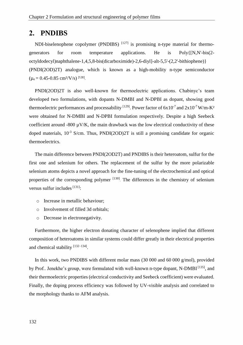
Chapter 2 Formulation and structural engineering of polymer films
132
PNDIBS
NDI-biselenophene copolymer (PNDIBS) [127] is promising n-type material for thermo-
generators for room temperature applications. He is Poly[N,N'-bis(2-
octyldodecyl)naphthalene-1,4,5,8-bis(dicarboximide)-2,6-diyl]-alt-5,5'-(2,2'-bithiophene)
(PNDI(2OD)2T) analogue, which is known as a high-mobility n-type semiconductor
(µe = 0.45-0.85 cm²/V/s) [128].
PNDI(2OD)2T is also well-known for thermoelectric applications. Chabinyc’s team
developed two formulations, with dopants N-DMBI and N-DPBI as dopant, showing good
thermoelectric performances and processability [129]. Power factor of 6x10⁻⁷ and 2x10⁻⁷ W/m-K²
were obtained for N-DMBI and N-DPBI formulation respectively. Despite a high Seebeck
coefficient around -800 µV/K, the main drawback was the low electrical conductivity of these
doped materials, 10-3 S/cm. Thus, PNDI(2OD)2T is still a promising candidate for organic
thermoelectrics.
The main difference between PNDI(2OD2T) and PNDIBS is their heteroatom, sulfur for the
first one and selenium for others. The replacement of the sulfur by the more polarizable
selenium atoms depicts a novel approach for the fine-tuning of the electrochemical and optical
properties of the corresponding polymer [130]. The differences in the chemistry of selenium
versus sulfur includes [131]:
o Increase in metallic behaviour;
o Involvement of filled 3d orbitals;
o Decrease in electronegativity.
Furthermore, the higher electron donating character of selenophene implied that different
composition of heteroatoms in similar systems could differ greatly in their electrical properties
and chemical stability [132–134].
In this work, two PNDIBS with different molar mass (30 000 and 60 000 g/mol), provided
by Prof.. Jenekhe’s group, were formulated with well-known n-type dopant, N-DMBI [135], and
their thermoelectric properties (electrical conductivity and Seebeck coefficient) were evaluated.
Finally, the doping process efficiency was followed by UV-visible analysis and correlated to
the morphology thanks to AFM analysis.

Chapter 2 Formulation and structural engineering of polymer films
133
The effect of n-doping on thermoelectric properties of PNDIBS was explored, results are
worked in Table 9. Polymer films were made in accordance with the procedure described in
Appendix II. Based on results Table 9 and Figure 31, molecular mass does not seem to have a
huge influence on thermoelectric properties. PNDBIS pristine thin films features an electrical
conductivity of 1.21 x 10⁻⁶ and 6.21 x 10⁻⁵ S/cm for 30 000 and 60 000 g/mol respectively. These
values are more than one order of magnitude higher than P(NDIOD-T2) doped with N-DMBI
[107]. N-DMBI concentration had a significant impact on thermoelectric properties. The highest
electrical conductivity was reached for 20 mol% of dopant for both molecular mass, 8 x 10⁻⁴
and 9 x 10⁻⁴ S/cm. After further doping, electrical conductivity dropped by nearly one order of
magnitude. For Seebeck coefficient, a decrease (absolute value) from -778 and -831 to -125 and
-156 µV/K happens when dopant concentration is increased. The power factor, S²σ, followed a
bell-shape trend with a maximum at 2.2 x 10⁻³ and 3.2 x 10⁻³ µW/m.K² for the low and the high
molecular mass respectively.
Molecular mass
(g/mol)
N-DMBI
conc. (mol%)
S (µV/K) σ (S/cm) PF
(µW/m.K²)
30 000
0 -778 ±25 2x10⁻⁸ 1.21x10⁻⁶
5 mol% -378 ±18 5x10⁻⁶ 7.14x10⁻⁵
10 mol% -223 ±11 6x10⁻⁵ 2.98x10⁻⁴
20 mol% -167 ±12 8x10⁻⁴ 2.2x10⁻³
30 mol% -125 ±10 1x10⁻⁴ 1.56x10⁻⁴
60 000
0 -831 ±17 9x10⁻⁷ 6.21x10⁻⁵
5 mol% -456 ±11 9x10⁻⁶ 1.87x10⁻⁴
10 mol% -264 ±20 4x10⁻⁵ 2.78x10⁻⁴
20 mol% -189 ±8 9x10⁻⁴ 3.2x10⁻³
30 mol% -156 ±12 1x10⁻⁵ 2.43x10⁻⁵
Table 9 : Thermoelectric properties of PNDIBS:N-DMBI thin films with different N-DMBI concentration
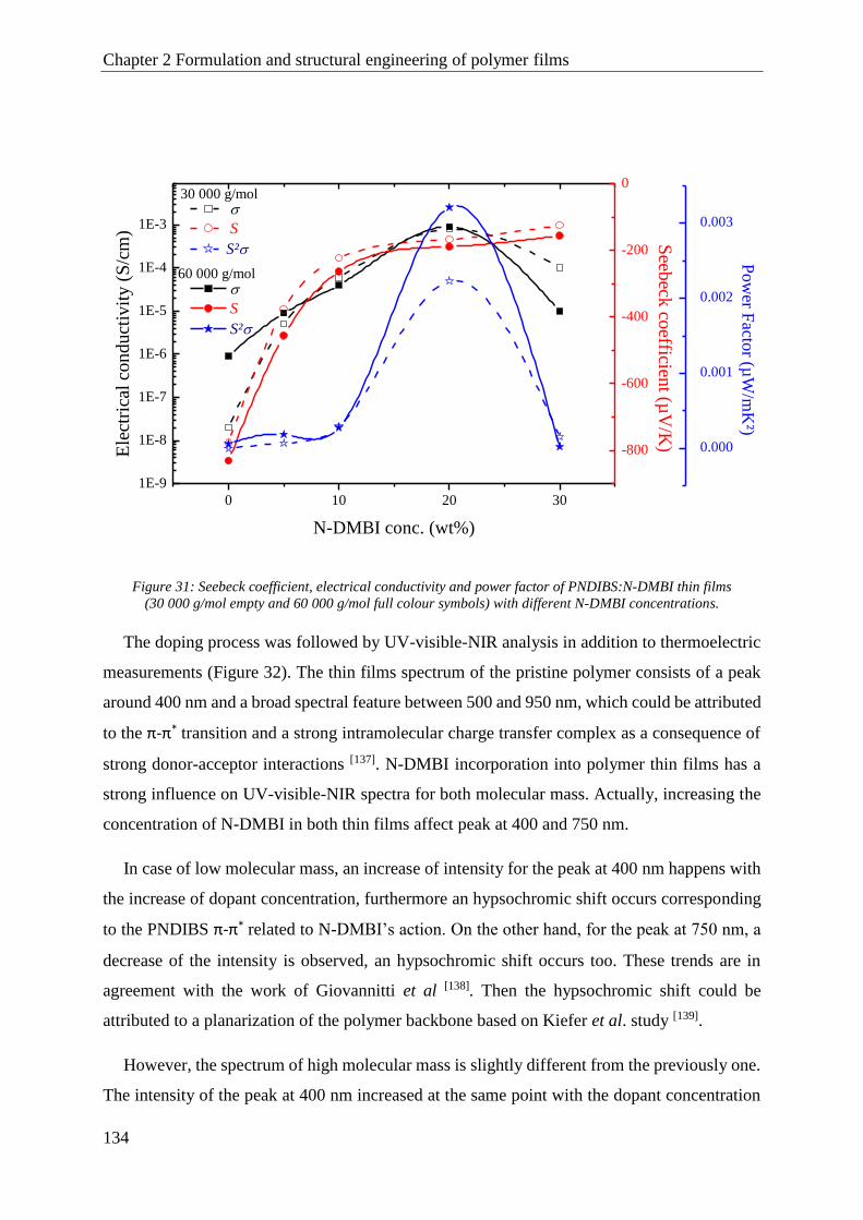
Chapter 2 Formulation and structural engineering of polymer films
134
0 10 20 30
1E-9
1E-8
1E-7
1E-6
1E-5
1E-4
1E-3
Ele
ctri
cal
con
du
ctiv
ity
(S
/cm
)
S
S²
S
S²
N-DMBI conc. (wt%)
30 000 g/mol
60 000 g/mol
-800
-600
-400
-200
0 S
eebeck
coefficien
t (µV
/K) 0.000
0.001
0.002
0.003
Pow
er Facto
r (µW
/mK
²)
Figure 31: Seebeck coefficient, electrical conductivity and power factor of PNDIBS:N-DMBI thin films
(30 000 g/mol empty and 60 000 g/mol full colour symbols) with different N-DMBI concentrations.
The doping process was followed by UV-visible-NIR analysis in addition to thermoelectric
measurements (Figure 32). The thin films spectrum of the pristine polymer consists of a peak
around 400 nm and a broad spectral feature between 500 and 950 nm, which could be attributed
to the π-π* transition and a strong intramolecular charge transfer complex as a consequence of
strong donor-acceptor interactions [137]. N-DMBI incorporation into polymer thin films has a
strong influence on UV-visible-NIR spectra for both molecular mass. Actually, increasing the
concentration of N-DMBI in both thin films affect peak at 400 and 750 nm.
In case of low molecular mass, an increase of intensity for the peak at 400 nm happens with
the increase of dopant concentration, furthermore an hypsochromic shift occurs corresponding
to the PNDIBS π-π* related to N-DMBI’s action. On the other hand, for the peak at 750 nm, a
decrease of the intensity is observed, an hypsochromic shift occurs too. These trends are in
agreement with the work of Giovannitti et al [138]. Then the hypsochromic shift could be
attributed to a planarization of the polymer backbone based on Kiefer et al. study [139].
However, the spectrum of high molecular mass is slightly different from the previously one.
The intensity of the peak at 400 nm increased at the same point with the dopant concentration
Chapter 2 Formulation and structural engineering of polymer films
135
of 5, 10 and 20 mol% but the decrease for 30 mol% to achieve almost the pristine intensity.
Then for the peak at 750 nm, the same phenomena as previously are observed, an intensity
decreasing and an hypsochromic shift.
400 500 600 700 800 900 10000.000
0.005
0.010
0.015
Abso
rpti
on
(a.
u.)
PNDIBS LM
PNDIBS LM 5 mol% N-DMBI
PNDIBS LM 10 mol% N-DMBI
PNDIBS LM 20 mol% N-DMBI
PNDIBS LM 30 mol% N-DMBI
Wavelength (nm)
400 500 600 700 800 900 10000.000
0.005
0.010
0.015
Ab
sorp
tio
n (
a.u
.)
PNDIBS HM
PNDIBS HM 5 mol% N-DMBI
PNDIBS HM 10 mol% N-DMBI
PNDIBS HM 20 mol% N-DMBI
PNDIBS HM 30 mol% N-DMBI
Wavelength (nm)
Figure 32: UV-visible spectra of (a) low molecular mass PNDIBS:N-DMBI and (b) high molecular mass
PNDIBS:N-DMBI thin films with different N-DMBI concentration
(a)
(b)
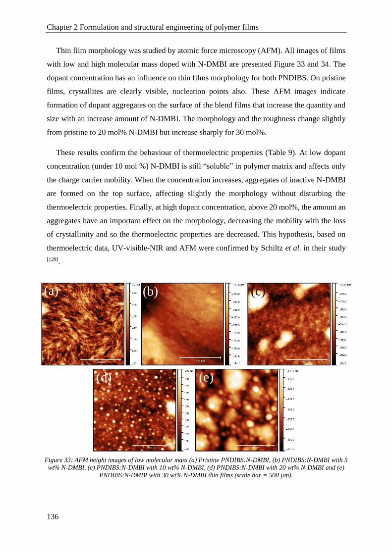
Chapter 2 Formulation and structural engineering of polymer films
136
Thin film morphology was studied by atomic force microscopy (AFM). All images of films
with low and high molecular mass doped with N-DMBI are presented Figure 33 and 34. The
dopant concentration has an influence on thin films morphology for both PNDIBS. On pristine
films, crystallites are clearly visible, nucleation points also. These AFM images indicate
formation of dopant aggregates on the surface of the blend films that increase the quantity and
size with an increase amount of N-DMBI. The morphology and the roughness change slightly
from pristine to 20 mol% N-DMBI but increase sharply for 30 mol%.
These results confirm the behaviour of thermoelectric properties (Table 9). At low dopant
concentration (under 10 mol %) N-DMBI is still “soluble” in polymer matrix and affects only
the charge carrier mobility. When the concentration increases, aggregates of inactive N-DMBI
are formed on the top surface, affecting slightly the morphology without disturbing the
thermoelectric properties. Finally, at high dopant concentration, above 20 mol%, the amount an
aggregates have an important effect on the morphology, decreasing the mobility with the loss
of crystallinity and so the thermoelectric properties are decreased. This hypothesis, based on
thermoelectric data, UV-visible-NIR and AFM were confirmed by Schiltz et al. in their study
[129].
Figure 33: AFM height images of low molecular mass (a) Pristine PNDIBS:N-DMBI, (b) PNDIBS:N-DMBI with 5
wt% N-DMBI, (c) PNDIBS:N-DMBI with 10 wt% N-DMBI, (d) PNDIBS:N-DMBI with 20 wt% N-DMBI and (e)
PNDIBS:N-DMBI with 30 wt% N-DMBI thin films (scale bar = 500 µm).
(b) (c)
(d) (e)
(a)
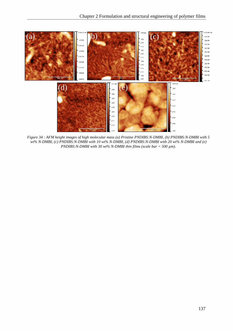
Chapter 2 Formulation and structural engineering of polymer films
137
Figure 34 : AFM height images of high molecular mass (a) Pristine PNDIBS:N-DMBI, (b) PNDIBS:N-DMBI with 5
wt% N-DMBI, (c) PNDIBS:N-DMBI with 10 wt% N-DMBI, (d) PNDIBS:N-DMBI with 20 wt% N-DMBI and (e)
PNDIBS:N-DMBI with 30 wt% N-DMBI thin films (scale bar = 500 µm).
(a) (b) (c)
(d) (e)

Chapter 2 Formulation and structural engineering of polymer films
138
C Conclusion
Through various processing modifications, the structural, electronic and thermoelectric
properties of various polymers and organic materials were tuned. Synthesized p-type polymers
showed better thermoelectric performances than supplied n-type materials. For instance in case
of PEDOT:Tos, a high power factor of 240 µW/mK² was achieved.
A novel polymer PNDIBS, analogue to PNDI(2OD)2T with selenium atoms, was tested as
a promising n-type thermoelectric material. Thermoelectric performances obtained for this
material were comparable with the PNDI(2OD)2T, known as a reference n-type material.
Unfortunately, the typical air sensibility of n-type material was noted.
Furthermore, this study shown the importance of fine doping of organic materials. In most
cases, the power factor followed a bell-shape curve with a maximum for a precise dopant
concentration.
Finally, these organic materials will be used as “brick” for the building of a thermoelectric
generator. Their performances will be enhanced thanks to inorganic materials and a novel
approach developed in our laboratory. Best thermoelectric performances of each material are
summarized in the Table 10.
Material
Dopant
or
structural
agent
Concentration
(wt% - mol%)
S
(µV/K)
σ
(S/cm)
PF
(µW/m.K²)
Air
stability
PEDOT:Tos DMSO
Pyridine
3
3 44 1240 240 Stable
P3HT m. F4TCNQ 20 76 4.3 2.48 Stable
P3HT seq. F4TCNQ 10 127 0.87 1.40 Stable
PCDTBT FeCl3 50 37 60 8.21 Stable
PTB7 DIO 3 760 0.017 0.9 Stable
PCBM AOB
N-DPBI
10
5 -412 0.7 11.88 Instable
PNDIBS LMn N-DMBI 20 -167 8x10⁻⁴ 2.2x10⁻³ Instable
PNDIBS HMn N-DMBI 20 -189 9x10⁻⁴ 3.2x10⁻³ Instable
Table 10 : Thermoelectric performances of best p- & n-type materials studied

Chapter 2 Formulation and structural engineering of polymer films
139
References
[1] Myer Kutz, Handbook of Environmental Degradation of Materials, Elsevier, "3rd
Edition", 2018, 684 (ISBN: 9780323524728).
[2] (a) J.-H. Bahk, H. Fang, K. Yazawa, A. Shakouri, J. Mater. Chem. C 2015, 3, 10362.
(b) L. K. Allison, T. L. Andrew, Adv. Mater. Technol. 2019, 4, 1800615
[3] O. Bubnova, "Thermoelectric properties of conducting polymers", PhD manuscript,
Department of Science and Technology, Linköping University: Norrköping, Sweden,
2013, 63 (ISBN: 978-91-7519-741-8).
[4] I. Petsagkourakis, "High performance polymer and polymer/inorganic thermoelectric
materials", PhD manuscript, LCPO-LOMA, Université de Bordeaux, Bordeaux
France, 2016 (NNT: 2016BOR0351).
[5] B. Lüssem, C.-M. Keum, D. Kasemann, B. Naab, Z. Bao, K. Leo, Chem. Rev. 2016,
116, 13714.
[6] L. Lu, T. Zheng, Q. Wu, A. M. Schneider, D. Zhao, L. Yu, Chem. Rev. 2015, 115,
12666.
[7] S. LeBlanc, Sustain. Mater. Technol. 2014, 1–2, 26.
[8] J. C. Hummelen, B. W. Knight, F. LePeq, F. Wudl, J. Yao, C. L. Wilkins, J. Org.
Chem. 1995, 60, 532.
[9] Y. Lan, A. J. Minnich, G. Chen, Z. Ren, Adv. Funct. Mater., 2010, 20 (3), 357-376.
[10] O. Bubnova, X. Crispin, Energy Environ. Sci. 2012, 5, 9345.
[11] G. J. Snyder, E. S. Toberer, Nature Materials, 2008, 7, 105-114.
[12] O. Bubnova, Z. U. Khan, H. Wang, S. Braun, D. R. Evans, M. Fabretto, P. Hojati-
Talemi, D. Dagnelund, J.-B. Arlin, Y. H. Geerts, S. Desbief, D. W. Breiby, J. W.
Andreasen, R. Lazzaroni, W. M. Chen, I. Zozoulenko, M. Fahlman, P. J. Murphy, M.
Berggren, X. Crispin, Nat. Mater. 2014, 13, 190.
[13] O. Bubnova, Z. U. Khan, A. Malti, S. Braun, M. Fahlman, M. Berggren, X. Crispin,
Nat. Mater. 2011, 10, 429.
[14] G.-H. Kim, L. Shao, K. Zhang, K. P. Pipe, Nat. Mater. 2013, 12, 719.
[15] I. Petsagkourakis, E. Pavlopoulou, G. Portale, B. A. Kuropatwa, S. Dilhaire, G. Fleury,
G. Hadziioannou, Scientific Works, 2016, 6, 30501.
[16] S. Ihnatsenka, X. Crispin, I. V. Zozoulenko, Phys. Rev. B 2015, 92, 035201.
[17] N. Kim, B. H. Lee, D. Choi, G. Kim, H. Kim, J.-R. Kim, J. Lee, Y. H. Kahng, K. Lee,
Phys. Rev. Lett. 2012, 109, 106405.
[18] B. B.-Y. Hsu, C.-M. Cheng, C. Luo, S. N. Patel, C. Zhong, H. Sun, J. Sherman, B. H.
Lee, L. Ying, M. Wang, G. Bazan, M. Chabinyc, J.-L. Brédas, A. Heeger, Adv. Mater.
2015, 27, 7759.
[19] J. Sun, M.-L. Yeh, B. J. Jung, B. Zhang, J. Feser, A. Majumdar, H. E. Katz,
Macromolecules 2010, 43, 2897.
[20] J. T. Rogers, K. Schmidt, M. F. Toney, G. C. Bazan, E. J. Kramer, J. Am. Chem. Soc.,
2012, 134 (6), 2884-2887.
[21] C. M. Palumbiny, F. Liu, T. P. Russell, A. Hexemer, C. Wang, P. Müller-Buschbaum,
Advanced Materials, 2015, 27 (22), 3391-3397.
[22] C. H. Woo, C. Piliego, T. W. Holcombe, M. F. Toney, J. M. J. Fréchet,
Macromolecules, 2012, 45 (7), 3057-3062.
[23] B. W. Boudouris, V. Ho, L. H. Jimison, M. F. Toney, A. Salleo, R. A. Segalman,
Macromolecules 2011, 44, 6653.
[24] B. Endrődi, J. Mellár, Z. Gingl, C. Visy, C. Janáky, J. Phys. Chem. C 2015, 119, 8472.

Chapter 2 Formulation and structural engineering of polymer films
140
[25] C. Goh, R. J. Kline, M. D. McGehee, E. N. Kadnikova, J. M. J. Fréchet, Appl. Phys.
Lett. 2005, 86, 122110.
[26] A. Zen et al., Macromolecules, 2006, 39 (6), 2162-2171.
[27] B. Winther-Jensen, D. W. Breiby, K. West, Synth. Met. 2005, 152, 1.
[28] J.-H. Huang, C.-W. Chu, Electrochimica Acta 2011, 56, 7228.
[29] C. Badre, L. MArquant, A. M. Alsayed, L. A. Hough, Advanced Functional Materials,
2012, 13 (22), 2723-2727.
[30] I. Petsagkourakis, E. Pavlopoulou, E. Cloutet, Y. F. Chen, X. Liu, M. Fahlman, M.
Berggren, X. Crispin, S. Dilhaire, G. Fleury, G. Hadziioannou, Org. Electron. 2018,
52, 335.
[31] L. Groenendaal, F. Jonas, D. Freitag, H. Pielartzik, J. R. Reynolds, Adv. Mater. 2000,
12, 481.
[32] XPS-Fitting, 2009, X-ray Photoelectron Spectroscopy (XPS) Reference Pages, view
on http://www.xpsfitting.com/2009/04/relative-sensitivity-factors-rsf.html (July,
2019).
[33] M. Fabretto, K. Zuber, C. Hall, P. Murphy, H. J. Griesser, J. Mater. Chem. 2009, 19,
7871.
[34] Q. Wei et al., Adv. Mater., 2015, 25, 2831-2836.
[35] N. Massonnet, A. Carella, A. de Geyer, J. Faure-Vincent, J.-P. Simonato, Chem. Sci.
2014, 6, 412.
[36] K. Zhang, S. Wang, J. Qiu, J. L. Blackburn, X. Zhang, A. J. Ferguson, E. M. Miller,
B. L. Weeks, Nano Energy 2016, 19, 128.
[37] D. Deribew et al., Macromolecules, 2013, 46 (8), 3015-3024.
[38] E. J. W. Crossland et al., Adv. MAter., 2012, 24, 839-844.
[39] X. Shen, V. Duzhko, T. P. Russell, Adv. Energy Mater. 2013, Sept 2012.
[40] K. E. Aasmundtveit, E. J. Samuelsen, L. A. A. Pettersson, O. Inganäs, T. Johansson,
R. Feidenhans’l, Synth. Met. 1999, 101, 561.
[41] H. Sirringhaus, P. J. Brown, R. H. Friend, M. M. Nielsen, K. Bechgaard, B. M. W.
Langeveld-Voss, A. J. H. Spiering, R. a. J. Janssen, E. W. Meijer, P. Herwig, D. M.
de Leeuw, Nature 1999, 401, 685.
[42] A. B. Kaiser, V. Skákalová, Chem. Soc. Rev. 2011, 40, 3786.
[43] W. Lövenich, Polym. Sci. Ser. C 2014, 56.
[44] A. Elschner, S. Kirchmeyer, W. Lovenich, U. Merker, K. Reuter, PEDOT: Principles
and Applications of an Intrinsically Conductive Polymer, CRC Press, 2010, 377
(ISBN: 9781420069112).
[45] Y-H. Ha et al., Adv. Funct. Mater., 2004, 14, No. 6, June.
[46] J.T. Rogers, K. Schmidt, M.F. Toney, G.C. Bazan, E.J. Kramer, J. Am. Chem. Soc.,
2012, 134 (6), 2884-7.
[47] G. Kollet et al., Science, 2007, 317 (5836), 351-355.
[48] X. Crispin et al. J. Am. Chem. Soc., 2004, 126 (38), 11889-11899.
[49] J. Clark, C. Silva, R. H. Friend, F. C. Spano, Phys. Rev. Lett. 2007, 98, 206406.
[50] R. D. McCullough, Adv. Mater. 1998, 10, 93.
[51] Y. Xie, S. Gao, M. Eslamian, Coatings 2015, 5, 488.
[52] F. C. Krebs, S. A. Gevorgyan, J. Alstrup, J. Mater. Chem. 2009, 19, 5442.
[53] Y. Lin, C.-F. Liu, Y.-J. Song, L. Yang, W.-J. Zeng, W.-Y. Lai, W. Huang, RSC Adv.
2016, 6, 40970.
[54] J.-F. Chang, B. Sun, D. W. Breiby, M. M. Nielsen, T. I. Sölling, M. Giles, I.
McCulloch, H. Sirringhaus, Chem. Mater. 2004, 16, 4772.
[55] M. L. Chabinyc, Y.-L. Loo, J. Macromol. Sci. Part C 2006, 46, 1.
Chapter 2 Formulation and structural engineering of polymer films
141
[56] L. J. A. Koster, E. C. P. Smits, V. D. Mihailetchi, P. W. M. Blom, Phys. Rev. B 2005,
72, 085205.
[57] S. E. Shaheen, C. J. Brabec, N. S. Sariciftci, F. Padinger, T. Fromherz, J. C.
Hummelen, Appl. Phys. Lett. 2001, 78, 841.
[58] G. Xie, Y. Jiang, X. Du, H. Tai, W. Li, Sensors, 2015, 15 (1), 2086-2103.
[59] J. W. Jeong, Y. W. Park, T. H. Park, J. H. Choi, H. J. Choi, E. H. Song, J. I. Lee, H.
Y. Chu, B. K. Ju, IEEE Electron Device Lett. 2011, 32, 348.
[60] Y. Yang, H. E. Katz, J. Mater. Chem. C 2017, 5, 2160.
[61] M. Y. Lee, H. J. Kim, G. Y. Jung, A.-R. Han, S. K. Kwak, B. J. Kim, J. H. Oh, Adv.
Mater. 2015, 27, 1540.
[62] E. Lim, K. A. Peterson, G. M. Su, M. L. Chabinyc, Chem. Mater. 2018, 30, 998.
[63] J. Hynynen, D. Kiefer, C. Müller, RSC Adv. 2018, 8, 1593.
[64] E. Jang, A. Poosapati, D. Madan, ACS Appl. Energy Mater. 2018, 1, 1455.
[65] M. Tonga, L. Wei, E. Wilusz, L. Korugic-Karasz, F. E. Karasz, P. M. Lahti, Synth.
Met. 2018, 239, 51.
[66] J. Obrzut, K. A. Page, Phys. Rev. B 2009, 80, 195211.
[67] J. Yu, Y. Zheng, J. Huang, Polymers 2014, 6, 2473.
[68] M. Chang, G. T. Lim, B. Park, E. Reichmanis, Polymers 2017, 9, 212.
[69] M. Brinkmann, J. Polym. Sci. Part B Polym. Phys. 2011, 49, 1218.
[70] S. D. Bergin, Z. Sun, D. Rickard, P. V. Streich, J. P. Hamilton, J. N. Coleman, ACS
Nano 2009, 3, 2340.
[71] C. J. Brabec, N. S. Sariciftci, J. C. Hummelen, Adv. Funct. Mater. 2001, 11, 15.
[72] Y. Lin, X. Zhan, Mater. Horiz. 2014, 1, 470.
[73] A. J. Heeger, J. Phys. Chem. B 2001, 105, 8475.
[74] P. Pingel, D. Neher, Phys. Rev. B 2013, 87, 115209.
[75] E. F. Aziz, A. Vollmer, S. Eisebitt, W. Eberhardt, P. Pingel, D. Neher, N. Koch, Adv.
Mater. 2007, 19, 3257.
[76] L. Ma, W. H. Lee, Y. D. Park, J. S. Kim, H. S. Lee, K. Cho, Appl. Phys. Lett. 2008,
92, 063310.
[77] P. Pingel, L. Zhu, K. S. Park, J.-O. Vogel, S. Janietz, E.-G. Kim, J. P. Rabe, J.-L.
Brédas, N. Koch, J. Phys. Chem. Lett. 2010, 1, 2037.
[78] I. Salzmann, G. Heimel, J. Electron Spectrosc. Relat. Phenom. 2015, 204, 208.
[79] L. Müller, D. Nanova, T. Glaser, S. Beck, A. Pucci, A. K. Kast, R. R. Schröder, E.
Mankel, P. Pingel, D. Neher, W. Kowalsky, R. Lovrincic, Chem. Mater. 2016, 28,
4432.
[80] J. Gao, E. T. Niles, J. K. Grey, J. Phys. Chem. Lett. 2013, 4, 2953.
[81] C. E. Johnson, D. S. Boucher, J. Polym. Sci. Part B Polym. Phys. 2014, 52, 526.
[82] M. Sapolsky, D. Boucher, J. Polym. Sci. Part B Polym. Phys. 2018, 56, 999.
[83] C. E. Johnson, M. P. Gordon, D. S. Boucher, J. Polym. Sci. Part B Polym. Phys. 2015,
53, 841.
[84] D. T. Scholes, P. Y. Yee, J. R. Lindemuth, H. Kang, J. Onorato, R. Ghosh, C. K.
Luscombe, F. C. Spano, S. H. Tolbert, B. J. Schwartz, Adv. Funct. Mater. 2017, 27,
1702654.
[85] I. E. Jacobs, E. W. Aasen, J. L. Oliveira, T. N. Fonseca, J. D. Roehling, J. Li, G. Zhang,
M. P. Augustine, M. Mascal, A. J. Moulé, J. Mater. Chem. C 2016, 4, 3454.
[86] G. Zuo, O. Andersson, H. Abdalla, M. Kemerink, Appl. Phys. Lett. 2018, 112, 083303.
[87] C. Wang, D. T. Duong, K. Vandewal, J. Rivnay, A. Salleo, Phys. Rev. B 2015, 91,
085205.
[88] R. Österbacka, Science 2000, 287, 839.

Chapter 2 Formulation and structural engineering of polymer films
142
[89] D. T. Duong, C. Wang, E. Antono, M. F. Toney, A. Salleo, Org. Electron. 2013, 14,
1330.
[90] I. E. Jacobs, E. W. Aasen, J. L. Oliveira, T. N. Fonseca, J. D. Roehling, J. Li, G. Zhang,
M. P. Augustine, M. Mascal, A. J. Moulé, J. Mater. Chem. C 2016, 4, 3454.
[91] D. T. Scholes, S. A. Hawks, P. Y. Yee, H. Wu, J. R. Lindemuth, S. H. Tolbert, B. J.
Schwartz, J. Phys. Chem. Lett. 2015, 6, 4786.
[92] I. E. Jacobs, J. Li, S. L. Burg, D. J. Bilsky, B. T. Rotondo, M. P. Augustine, P. Stroeve,
A. J. Moulé, ACS Nano 2015, 9, 1905.
[93] J. Y. Lek, Y. M. Lam, J. Niziol, M. Marzec, Nanotechnology 2012, 23, 315401.
[94] J. S. Moon, J. Jo, A. J. Heeger, Adv. Energy Mater. 2012, 2, 304.
[95] S. Cho, J. H. Seo, S. H. Park, S. Beaupré, M. Leclerc, A. J. Heeger, Adv. Mater.
Deerfield Beach Fla 2010, 22, 1253.
[96] S. Wakim, B-R Aïch, Y. Tao, M. Leclerc, Polymer Reviews, 2007, 48 (3), 432-462.
[97] M. Culebras, C. M. Gómez, A. Cantarero, Materials 2014, 7, 6701.
[98] I. Lévesque, P.-O. Bertrand, N. Blouin, M. Leclerc, S. Zecchin, G. Zotti, C. I. Ratcliffe,
D. D. Klug, X. Gao, F. Gao, J. S. Tse, Chem. Mater. 2007, 19, 2128.
[99] I. Lévesque, X. Gao, D. D. Klug, J. S. Tse, C. I. Ratcliffe, M. Leclerc, React. Funct.
Polym. 2005, 65, 23.
[100] J. Maiz, M. M. Rojo, B. Abad, A. A. Wilson, A. Nogales, D.-A. Borca-Tasciuc, T.
Borca-Tasciuc, M. Martín-González, RSC Adv. 2015, 5, 66687.
[101] R. B. Aïch, N. Blouin, A. Bouchard, M. Leclerc, Chem. Mater. 2009, 21, 751.
[102] G. J. Snyder, Energy Harvesting Technologies, Springer, Boston, MA, 2009; pp. 325–
336.
[103] L. Lu, L. Yu, Adv. Mater. 2014, 26, 4413.
[104] Y. Liang, Z. Xu, J. Xia, S.-T. Tsai, Y. Wu, G. Li, C. Ray, L. Yu, Adv. Mater. 2010,
22, E135.
[105] W. Kim, J. K. Kim, E. Kim, T. K. Ahn, D. H. Wang, J. H. Park, J. Phys. Chem. C
2015, 119, 5954.
[106] S. Das, J. K. Keum, J. F. Browning, G. Gu, B. Yang, O. Dyck, C. Do, W. Chen, J.
Chen, I. N. Ivanov, K. Hong, A. J. Rondinone, P. C. Joshi, D. B. Geohegan, G.
Duscher, K. Xiao, Nanoscale 2015, 7, 15576.
[107] T. Han, L. Liu, M. Wei, C. Wang, X. Wu, Z. Xie, Y. Ma, Phys. Chem. Chem. Phys.
2017, 19, 17653.
[108] Z. He, C. Zhong, S. Su, M. Xu, H. Wu, Y. Cao, Nat. Photonics 2012, 6, 591.
[109] Z. He, C. Zhong, X. Huang, W.-Y. Wong, H. Wu, L. Chen, S. Su, Y. Cao, Adv. Mater.
2011, 23, 4636.
[110] B. Carsten, J. M. Szarko, H. J. Son, W. Wang, L. Lu, F. He, B. S. Rolczynski, S. J.
Lou, L. X. Chen, L. Yu, J. Am. Chem. Soc. 2011, 133, 20468.
[111] A. Solanki et al., J. Phys. Chem. C, 2014, 118 (21), 11285-11291.
[112] M. Rastegaralam, C. Lee, U. Dettlaff-Weglikowska, Crystals 2017, 7, 292.
[113] C. J. M. Lasance, 2006, The Seebeck Coefficient., view on https://www.electronics-
cooling.com/2006/11/the-seebeck-coefficient/ (July, 2019).
[114] S. J. Lou, N. Zhou, X. Guo, R. P. H. Chang, T. J. Marks, L. X. Chen, J. Mater. Chem.
A 2018, 6, 23805.
[115] J. Ho Youn, Y. Il Lee, H. Tae Moon, M. Sun Ryu, J. Kim, J. Jang, Curr. Appl. Phys.
2010, 10.
[116] Y.-Y. Lai, Y.-J. Cheng, C.-S. Hsu, Energy Environ. Sci. 2014, 7, 1866.
[117] P. Cheng, C. Yan, T.-K. Lau, J. Mai, X. Lu, X. Zhan, Adv. Mater. 2016, 28, 5822.
[118] W. Chen, Y. Wu, Y. Yue, J. Liu, W. Zhang, X. Yang, H. Chen, E. Bi, I. Ashraful, M.
Grätzel, L. Han, Science 2015, 350, 944.
Chapter 2 Formulation and structural engineering of polymer films
143
[119] P.-W. Liang, C.-C. Chueh, S. T. Williams, A. K.-Y. Jen, Adv. Energy Mater. 2015, 5,
1402321.
[120] J. Yang, H.-L. Yip, A. K.-Y. Jen, Adv. Mater. Funct. 2013, 3 (5), 549-565.
[121] P. Wei, J. H. Oh, G. Dong, Z. Bao, J. Am. Chem. Soc. 2010, 132, 8852.
[122] F. Gao, Y. Liu, Y. Xiong, P. Wu, B. Hu, L. Xu, Front. Optoelectron. 2017, 10, 117.
[123] F. Li, M. Pfeiffer, A. Werner, K. Harada, K. Leo, N. Hayashi, K. Seki, X. Liu, X.-D.
Dang, J. Appl. Phys. 2006, 100, 023716.
[124] G. Zuo, Z. Li, E. Wang, M. Kemerink, Adv. Electron. Mater. 2018, 4, 1700501.
[125] M. Pietrzak, M. Szabelski, A. Kasparek, Z. Wieczorek, Chem. Phys. Lett. 2017, 669,
85.
[126] Y. Lu, J.-Y. Wang, J. Pei, Angew. Chem. Int. Ed., 2019, 58, 1-6.
[127] N. B. Kolhe, H. Lee, D. Kuzuhara, N. Yoshimoto, T. Koganezawa, S. A. Jenekhe,
Chem. Mater. 2018, 30, 6540.
[128] H. Yan, Z. Chen, Y. Zheng, C. Newman, J. R. Quinn, F. Dötz, M. Kastler, A. Facchetti,
Nature 2009, 457, 679.
[129] R. A. Schlitz, F. G. Brunetti, A. M. Glaudell, P. L. Miller, M. A. Brady, C. J. Takacs,
C. J. Hawker, M. L. Chabinyc, Adv. Mater. 2014, 26, 2825.
[130] E. Aqad, M. V. Lakshmikantham, M. P. Cava, Org. Lett. 2001, 3, 4283.
[131] M. D. Bezoari, P. Kovacic, S. Gronowitz, A.-B. Hörnfeldt, J. Polym. Sci. Polym. Lett.
Ed. 1981, 19, 347.
[132] S. J. Xie, L. M. Mei, D.L. Lin, Phys. Rev. B Condens. Matter 1994, 50, 13364.
[133] H. O. Villar, P. Otto, M. Dupuis, J. Ladik, Synth. Met. 1993, 59, 97.
[134] J. Xu, J. Hou, S. Zhang, G. Nie, S. Pu, L. Shen, Q. Xiao, J. Electroanal. Chem. 2005,
578, 345.
[135] L. Tu, X. Wang, J. Wang, X. Meng, J. Chu, Adv. Electron. Mater. 2018, 4, 1870051.
[136] R. A. Schlitz, F. G. Brunetti, A. M. Glaudell, P. L. Miller, M. A. Brady, C. J. Takacs,
C. J. Hawker, M. L. Chabinyc, Adv. Mater. Deerfield Beach Fla 2014, 26, 2825.
[137] Y.-J. Hwang, G. Ren, N. M. Murari, S. A. Jenekhe, Macromolecules 2012, 45, 9056.
[138] A. Giovannitti, C. B. Nielsen, D.-T. Sbircea, S. Inal, M. Donahue, M. R. Niazi, D. A.
Hanifi, A. Amassian, G. G. Malliaras, J. Rivnay, I. McCulloch, Nat. Commun. 2016,
7, 13066.
[139] D. Kiefer, A. Giovannitti, H. Sun, T. Biskup, A. Hofmann, M. Koopmans, C. Cendra,
S. Weber, L. J. Anton Koster, E. Olsson, J. Rivnay, S. Fabiano, I. McCulloch, C.
Müller, ACS Energy Lett. 2018, 3, 278.

144
Chapter 3 Hybrid polymer-inorganic material tailoring
145
Chapter 3
Hybrid polymer-inorganic material
tailoring
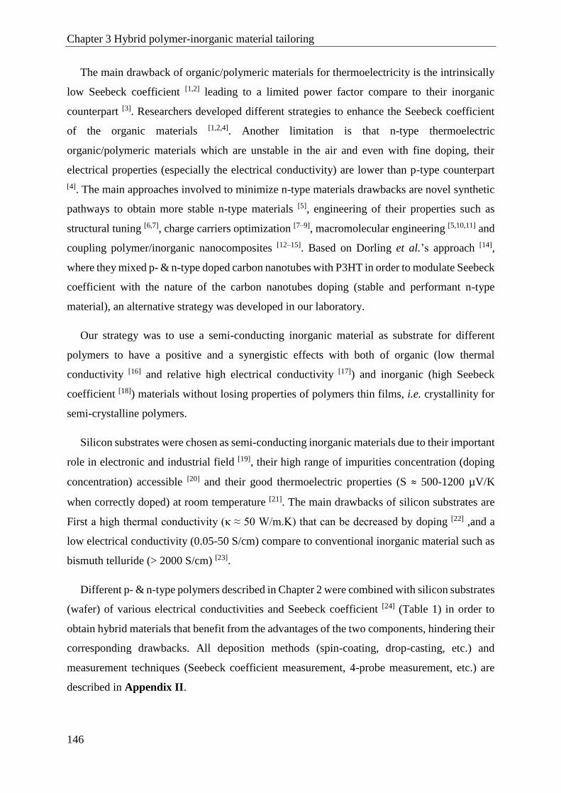
Chapter 3 Hybrid polymer-inorganic material tailoring
146
The main drawback of organic/polymeric materials for thermoelectricity is the intrinsically
low Seebeck coefficient [1,2] leading to a limited power factor compare to their inorganic
counterpart [3]. Researchers developed different strategies to enhance the Seebeck coefficient
of the organic materials [1,2,4]. Another limitation is that n-type thermoelectric
organic/polymeric materials which are unstable in the air and even with fine doping, their
electrical properties (especially the electrical conductivity) are lower than p-type counterpart
[4]. The main approaches involved to minimize n-type materials drawbacks are novel synthetic
pathways to obtain more stable n-type materials [5], engineering of their properties such as
structural tuning [6,7], charge carriers optimization [7–9], macromolecular engineering [5,10,11] and
coupling polymer/inorganic nanocomposites [12–15]. Based on Dorling et al.’s approach [14],
where they mixed p- & n-type doped carbon nanotubes with P3HT in order to modulate Seebeck
coefficient with the nature of the carbon nanotubes doping (stable and performant n-type
material), an alternative strategy was developed in our laboratory.
Our strategy was to use a semi-conducting inorganic material as substrate for different
polymers to have a positive and a synergistic effects with both of organic (low thermal
conductivity [16] and relative high electrical conductivity [17]) and inorganic (high Seebeck
coefficient [18]) materials without losing properties of polymers thin films, i.e. crystallinity for
semi-crystalline polymers.
Silicon substrates were chosen as semi-conducting inorganic materials due to their important
role in electronic and industrial field [19], their high range of impurities concentration (doping
concentration) accessible [20] and their good thermoelectric properties (S ≈ 500-1200 µV/K
when correctly doped) at room temperature [21]. The main drawbacks of silicon substrates are
First a high thermal conductivity (κ ≈ 50 W/m.K) that can be decreased by doping [22] ,and a
low electrical conductivity (0.05-50 S/cm) compare to conventional inorganic material such as
bismuth telluride (> 2000 S/cm) [23].
Different p- & n-type polymers described in Chapter 2 were combined with silicon substrates
(wafer) of various electrical conductivities and Seebeck coefficient [24] (Table 1) in order to
obtain hybrid materials that benefit from the advantages of the two components, hindering their
corresponding drawbacks. All deposition methods (spin-coating, drop-casting, etc.) and
measurement techniques (Seebeck coefficient measurement, 4-probe measurement, etc.) are
described in Appendix II.

Chapter 3 Hybrid polymer-inorganic material tailoring
147
Charge carriers type Nickname σ
(S/cm)
S
(µV/K)
Positive type silicon (holes)
p-Si (0.05) 0.05 1052
p-Si (0.7) 0.7 1001
p-Si (20) 20 851
p-Si (50) 50 760
Negative type silicon (electrons)
n-Si (0.05) 0.05 -1000
n-Si (0.7) 0.7 -951
n-Si (20) 20 -800
n-Si (50) 50 -701
Table 1: Electrical conductivity and Seebeck coefficient measured of different Silicon wafers used.
Hybrid PEDOT:Tos-silicon material
PEDOT:Tos thin films were deposited on top of silicon wafers, by in-situ polymerization,
following the procedure described in Appendix II. The best formulation, with pyridine and
DMSO, was used (electrical conductivity = 1200 S/cm and Seebeek coefficient = 44 µV/K).
The influence of PEDOT:Tos thickness on thermoelectric properties of the hybrid material was
investigated. Results obtained were confirmed by UPS and XPS analysis.
1.1 Seebeck coefficient
First, the influence of PEDOT:Tos thickness on Si substrates of various
doping/conductivities was studied by measuring the Seebeck coefficient (Figure 1). The doping
type (positive or negative) does not have an effect on absolute Seebeck coefficient value, a
superposition of Seebeck coefficient for p- & n-type Silicon for each PEDOT:Tos thicknesses
is possible. However, depending on the Si substrates conductivities, the Seebeck coefficient has
different behaviour with respect of PEDOT:Tos thicknesses.
For silicon with low conductivities (0.05 and 0.7 S/cm), Seebeck coefficient decreases
rapidly when the PEDOT:Tos thickness increases, and reaches a plateau value after five
polymer layers near the Seebeck coefficient of PEDOT:Tos (44 µV/K). In case of silicon with
high conductivities (20 and 50 S/cm), Seebeck coefficient decreases slowly with the increase
of PEDOT:Tos thickness, and a plateau value is achieved after two/three polymer layers.
PEDOT:Tos on p-type silicon has a positive Seebeck coefficient and a negative one on n-type
silicon, showing the strong influence of the substrate doping nature on Seebeck coefficient. The

Chapter 3 Hybrid polymer-inorganic material tailoring
148
plateau value for thick polymer thicknesses shows a strong dependence to the intrinsic
properties of the substrate. This approach allows the tuning of the Seebeck coefficient (value
and type of charge carriers) depending on the doping of the substrate and the polymer thickness.
0 2 4 6 8-1200
-800
-400
0
400
800
1200
n-type
PEDOT:Tos
0.05 S/cm
0.05 S/cm
0.7 S/cm
0.7 S/cm
20 S/cm
20 S/cm
50 S/cm
50 S/cm
See
bec
k C
oef
fici
ent
(µV
/K)
Number of layers
p-type
44 µV/K
Figure 14: Seebeck coefficient plotted versus number of PEDOT:Tos layers.
Blue symbols are for n-type silicon and red symbols are for p-type silicon. Each symbols correspond to an
electrical conductivity of a silicon substrate: dots 0.05 S/cm, inverted triangles 0.7 S/cm, diamonds 20 S/cm and
stars 50 S/cm. Dashed line is the Seebeck coefficient of bare PEDOT:Tos.
This behaviour was investigated thanks to a model considering the PEDOT:Tos-silicon
system as described in Figure 2b. From an electrical point of view, the thermoelectric layers are
modelled as a Seebeck generator (S.ΔT) in series with its electrical sheet resistance (σ.t)
(Figure 2a). In case of PEDOT:Tos-silicon system, the same basic system is applied, giving two
sources with resistances in parallel (Figure 2b). When this “more” complex model is applied to
the experimental data, the total Seebeck coefficient for this kind of junction is calculated with
the following expression (Equation 1):

Chapter 3 Hybrid polymer-inorganic material tailoring
149
𝑆𝐽𝑢𝑛𝑐𝑡𝑖𝑜𝑛 = 𝑆𝑆𝑖 .1 +
𝑆𝑝𝑜𝑙 . 𝜎𝑝𝑜𝑙.𝑡𝑝𝑜𝑙
𝑆𝑆𝑖. 𝜎𝑆𝑖 . 𝑡𝑆𝑖
1 + 𝜎𝑝𝑜𝑙 .𝑡𝑝𝑜𝑙
𝜎𝑆𝑖. 𝑡𝑆𝑖
(1)
𝑡𝑝𝑜𝑙 → 0 ; 𝑆𝑗𝑢𝑛𝑐𝑡𝑖𝑜𝑛 = 𝑆𝑆𝑖
𝑡𝑝𝑜𝑙 → ∞ ; 𝑆𝑗𝑢𝑛𝑐𝑡𝑖𝑜𝑛 = 𝑆𝑝𝑜𝑙
where the Seebeck coefficient (Spol and SSi), the electrical conductivity (σpol and σSi) and the
thickness (tpol and tSi) of PEDOT:Tos and silicon substrate are expressed, respectively.
Resulting calculated Seebeck coefficient data are plotted and compared to experimental
Seebeck coefficient in Figure 3. This model (dashed line) allows to satisfactorily fit the
experimental data (“dots”) for PEDOT:Tos-silicon junction with high electrical conductivities.
However, depending on the silicon substrates conductivities, the Seebeck coefficient has a
different behaviour with respect of PEDOT:Tos thicknesses (number of layers). In case of low
conductive silicon substrates (circles and inverted triangles), the measured Seebeck coefficient
of the thinner PEDOT:Tos samples (zero to five polymer layers) decreases when the polymer
thickness increases, and then reaches the same order of magnitude as the one of the PEDOT:Tos
on glass (black dashed lines) after five polymers layers. On the other hand, for high conductive
silicon substrate (diamonds and stars), the measured Seebeck coefficient of PEDOT:Tos
samples reaches a plateau after only one layer. Consequently, this approach allows the tuning
of the Seebeck coefficient value and sign depending on the doping of the substrate. Hybrid
PEDOT:Tos–silicon samples with a negative Seebeck coefficient are air stable. Interestingly
the plateau value obtained for PEDOT:Tos film shows a strong dependence to the intrinsic
Figure 2: (a) Model system for a thermoelectric material composed of voltage source (S) and resistance (R)
connected in series.
(b) Model system for hybrid material (silicon and PEDOT:Tos) composed of two identical model from (a) in
parallel.
(a) (b)

Chapter 3 Hybrid polymer-inorganic material tailoring
150
conductivity of the Si substrates. One hypothesis to understand the poor fitting at lower
thicknesses could be the presence of an additional interaction at the interface, which was not
take into account in the model, between the silicon substrate and the polymer. More analysis,
UPS and XPS analysis would give information about this possible phenomenon.
.
0 2 4 6 8-1200
-900
-600
-300
0
300
600
900
1200
PEDOT:Tos
0.05 S/cm
Model 0.05 S/cm
0,7 S/cm
Model 0.7 S/cm
20 S/cm
Model 20 S:cm
50 S/cm
Model 50 S/cm
See
bec
k c
oef
fici
ent
(µV
/K)
Number of layers
p-type
n-type
44 µV/K
Figure 3: Seebeck coefficient plotted versus number of PEDOT:Tos layers.
Color dashed lines are for the model obtained with Equation 1 and symbols are for experimental data.
Each color/symbol corresponds to an electrical conductivity of a silicon substrate: red dots 0.05 S/cm, blue
inverted triangles 0.7 S/cm, green diamonds 20 S/cm and orange stars 50 S/cm. Black dashed line is the Seebeck
coefficient of bare PEDOT:Tos.
As shown in Chapter 2, the Seebeck coefficient of polymers is dependent of their Density of
States (DoS). So, if the shape of the DoS, the filling of the DoS, or the Fermi level position
change, that will affect the material thermoelectric behaviour [7,9]. As described in the literature,
the shape of DoS for a polymer/nanocomposite material is affected by both the DoS of the
polymer and the DoS of the inorganic part [15]. So PEDOT:Tos on various silicon substrates
should result in hybrid materials of different DoS, and confirm Seebeck coefficients observed.
First, Ultraviolet Photoelectron Spectroscopy (UPS) was performed on bare silicon, the
influence of the doping (type and concentration of impurities) was studied (Figure 4a). The
shape of bare silicon curves is in accordance with results in literature [25], the work function
extracted is 4.2 eV and 4.3 eV for low and high conductive bare silicon respectively. Thanks to
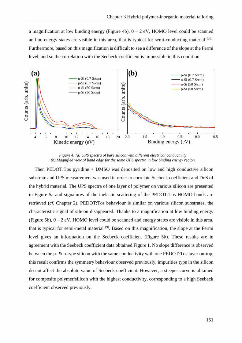
Chapter 3 Hybrid polymer-inorganic material tailoring
151
a magnification at low binding energy (Figure 4b), 0 – 2 eV, HOMO level could be scanned
and no energy states are visible in this area, that is typical for semi-conducting material [26].
Furthermore, based on this magnification is difficult to see a difference of the slope at the Fermi
level, and so the correlation with the Seebeck coefficient is impossible in this condition.
Then PEDOT:Tos pyridine + DMSO was deposited on low and high conductive silicon
substrate and UPS measurement was used in order to correlate Seebeck coefficient and DoS of
the hybrid material. The UPS spectra of one layer of polymer on various silicon are presented
in Figure 5a and signatures of the inelastic scattering of the PEDOT:Tos HOMO bands are
retrieved (cf. Chapter 2). PEDOT:Tos behaviour is similar on various silicon substrates, the
characteristic signal of silicon disappeared. Thanks to a magnification at low binding energy
(Figure 5b), 0 – 2 eV, HOMO level could be scanned and energy states are visible in this area,
that is typical for semi-metal material [9]. Based on this magnification, the slope at the Fermi
level gives an information on the Seebeck coefficient (Figure 5b). These results are in
agreement with the Seebeck coefficient data obtained Figure 1. No slope difference is observed
between the p- & n-type silicon with the same conductivity with one PEDOT:Tos layer on-top,
this result confirms the symmetry behaviour observed previously, impurities type in the silicon
do not affect the absolute value of Seebeck coefficient. However, a steeper curve is obtained
for composite polymer/silicon with the highest conductivity, corresponding to a high Seebeck
coefficient observed previously.
2.0 1.5 1.0 0.5 0.0 -0.5
Co
un
ts (
arb
. u
nit
s)
Binding energy (eV)
p-Si (0.7 S/cm)
n-Si (0.7 S/cm)
n-Si (50 S/cm)
p-Si (50 S/cm)
4 6 8 10 12 14 16 18 20
n-Si (0.7 S/cm)
p-Si (0.7 S/cm)
n-Si (50 S/cm)
p-Si (50 S/cm)
Co
un
ts (
arb
. u
nit
s)
Kinetic energy (eV)
(a) (b)
Figure 4: (a) UPS spectra of bare silicon with different electrical conductivity.
(b) Magnified view of band edge for the same UPS spectra in low binding energy region.

Chapter 3 Hybrid polymer-inorganic material tailoring
152
Thereafter, UPS analysis was conducted on PEDOT:Tos-silicon composite with different
PEDOT:Tos thicknesses in order to investigate and confirm the influence of polymer on the
Seebeck coefficient (Figure 6). For more readability, only magnification (0 – 2 eV area) of one
low (σ=0.7 S/cm) and one high conductive silicon is presented. In case of low conductive
silicon, the addition of polymer on-top of silicon have an influence on the slope at the Fermi
level, which is less steep with the addition of PEDOT:Tos. So, the Seebeck coefficient follow
the same trend by being lower with PEDOT:Tos addition as found from measurement and
model. On the other side, polymer thickness do not have any influence for PEDOT:Tos-high
conductive silicon as expected (Figure 1).
Figure 6: Magnified view of UPS spectra in low binding energy region for different PEDOT:Tos thickness on
silicon with (a) low electrical conductivity and (b) high electrical conductivity.
2.0 1.5 1.0 0.5 0.0 -0.5
Co
un
ts (
arb.
un
its)
Binding energy (eV)
1 layer PEDOT on n-Si (0.7 S/cm)
3 layer PEDOT on n-Si (0.7 S/cm)
7 layer PEDOT on n-Si (0.7 S/cm)
2.0 1.5 1.0 0.5 0.0 -0.5
Co
un
ts (
arb.
un
its)
Binding energy (eV)
1 layer PEDOT on n-Si (50 S/cm)
3 layer PEDOT on n-Si (50 S/cm)
7 layer PEDOT on n-Si (50 S/cm)
Figure 55: (a) UPS spectra of 1 layer of PEDOT:Tos on silicon with different electrical conductivities.
(b) Magnified view of band edges for the same UPS spectra in low binding energy region.
(a) (b)
4 6 8 10 12 14 16 18 20
Co
un
ts (
arb.
un
its)
Kinetic energy (eV)
PEDOT on glass
PEDOT on n-Si (0.7 S/cm)
PEDOT on p-Si (0.7 S/cm)
PEDOT on n-Si (50 S/cm)
2.0 1.5 1.0 0.5 0.0 -0.5
Co
un
ts (
arb
. u
nit
s)
Binding energy (eV)
PEDOT on glass
PEDOT on n-Si (0.7 S/cm)
PEDOT on p-Si (0.7 S/cm)
PEDOT on n-Si (50 S/cm)
(a) (b)

Chapter 3 Hybrid polymer-inorganic material tailoring
153
The change of Seebeck coefficient for this hybrid materials can’t be properly attributed to a
charge transfer between PEDOT:Tos and silicon substrate based on UPS measurement.
However, despite UPS is a strong tool, is limited to the surface effects [27]. As it was shown
Chapter 1, the Seebeck coefficient is dependant of charge carriers concentration, N. Increasing
N results in a decreasing of the Seebeck coefficient value. So in order to determine the oxidation
level linked to N, XPS analysis was conducted on Si (σ=50 S/cm)/PEDOT:Tos composite at
different polymer thicknesses (Figure 7). The oxidation level extracted from these analysis
(cf. Chapter 2 for Oxidation level calculation and Appendix II) is similar, indicating that the
polymer thickness does not affect the number of charge carriers. It seems this behaviour could
be only explained by the average of contribution for each Seebeck coefficient from each
material as proven by the developed model.
Figure 7: S(2p) XPS spectra for different PEDOT :Tos film thicknesses on silicon (σ= 50 S/cm).
Blue and red lines represent the fit of PEDOT unit and tosylate counter-ion, respectively (More details in the
Appendix II).
162 164 166 168 170 172
Co
un
ts (
arb
. u
nit
s)
Binding Energy (eV)
1 layer
3 layers
7 layers

Chapter 3 Hybrid polymer-inorganic material tailoring
154
1.2 Electrical conductivity
The effective electrical conductivity of previous devices, σjunction, was measured to
investigate the role of the interface in these PEDOT:Tos-silicon junctions. σjunction could be
extracted from the sheet resistance (R) of the hybrid device (Equation 2). The same substrate
architecture and treatment, described in Appendix II, was used for the measurement.
1
𝑅 = 𝜎𝐽𝑢𝑛𝑐𝑡𝑖𝑜𝑛. (𝑡𝑆𝑖+𝑡𝑝𝑜𝑙) = 𝜎𝑆𝑖𝑡𝑆𝑖 + 𝜎𝑝𝑜𝑙𝑡𝑝𝑜𝑙
⇒ 𝜎𝐽𝑢𝑛𝑐𝑡𝑖𝑜𝑛 =
𝜎𝑆𝑖𝑡𝑆𝑖 + 𝜎𝑝𝑜𝑙𝑡𝑝𝑜𝑙
𝑡𝑆𝑖+𝑡𝑝𝑜𝑙
(2)
As seen before, a thermoelectric material could be interpreted, from electrical point of view,
as a Seebeck generator (S.ΔT) in series with its electrical sheet resistance (σ.t). The electrical
sheet resistance of hybrid PEDOT:Tos/Si have to be determine without the “Seebeck generator”
that could interfere. The experimental translation was to apply an “high current” (compare to
Seebeck measurement = 1 nA) of 1 mA to “supress” the generators (Figure 8).
Figure 86: Model system for a hybrid thermoelectric material composed of resistances (R) connected in parallel.
Voltage sources are suppressed due to “high” current applied.
Unfortunately, by applying a current on a thermoelectric material, Thomson or Joule effect
could occur and interfere in electrical conductivity measurement (Appendix II). In case of
Thomson effect, when a material is submitted to a temperature gradient and an electrical
current, heat from outside environment can be exchanged (absorption or release) [28].
Furthermore, an electrical current passing through an electrical conductor increases the internal

Chapter 3 Hybrid polymer-inorganic material tailoring
155
energy of the system producing heat increase, so-called Joule effect, a temperature gradient
could be generated and modified the system [29]. In order to investigate these possible
interferences, a thermal imaging camera was used and pictures are presented Figure 9.
Figure 9: Thermal images of home-made Seebeck coefficient measurement system in various conditions
captured with an infrared thermal camera.
In all cases, an electrical current of 1 mA was applied during recording, three different
experiments were done:
o Figure 9a, without temperature difference at room temperature;
o Figure 9b, 25 °C applied on both sides;
o Figure 9c, a temperature gradient of 5°C applied (23 °C on left and 28 °C on right side).
Due to the low emissivity of metals, scotch tape was put on Peltier plates in order to measure
and confirm the temperature applied [30]. For image (a), the same homogeneous colour on Peltier
plates and sample allow to say that no Joule effect happens when a “high” current is applied.
Then, image (b) where each side are heated at 25 °C confirm the absence of Thomson effect,
no hot point is visible on the sample when temperature and “high” current is applied at the same
time. Finally, the last image (c), a temperature difference is applied between each Peltier plates,
a temperature gradient is visible on the sample and no heat absorption or emission is present
during the measurement. In summary, thanks to these thermal imaging, none Joule effect nor
Thomson effect are visible, confirming that experimental settings are valid for electrical
conductivity measurement.

Chapter 3 Hybrid polymer-inorganic material tailoring
156
The influence of PEDOT:Tos thickness on the conductivity of various Si substrates was
studied (Figure 10, two graphics were drawn to improve the visibility). The electrical
conductivity was indirectly obtained by electrical resistance measurement and by applying the
following equation (Appendix II):
𝜌 = 1
𝜎 = 𝑅
𝑤 . 𝑡
𝐿 (3)
Where the resistivity (ρ), the electrical conductivity (σ), the resistance (R), the width (w), the
thickness (t) and the length (L) are expressed. Due to the 2-probes measurement, the contact
resistance was determined [31,32] and subtracted to all resistance values as explained more
precisely in Appendix II.
The doping type (positive in red and negative in blue) does not have a significant effect on
electrical conductivity values regarding the experimental standard deviation. But, depending on
the Si substrate conductivity, the effective conductivity values are different. Principally, an
increase of polymer thickness induces an increase of the electrical conductivity until the five
PEDOT:Tos layer then a plateau is achieved. In an unexpected way, the substrate conductivity
has an influence on the composite material. In case of low conductive silicon, PEDOT:Tos layer
stacking produces a small increase of the overall electrical conductivity. PEDOT:Tos layer
0 2 4 6 80
1
2
3
Ju
nct
ion (
S/c
m)
0.05 S/cm (p)
0.05 S/cm (n)
0.7 S/cm (p)
0.7 S/cm (n)
Number of layers0 2 4 6 8
0
50
100
150
200
Ju
nct
ion (
S/c
m)
20 S/cm (p)
20 S/cm (n)
50 S/cm (p)
50 S/cm (n)
Number of layers
Figure 10: Electrical conductivity of the junction plotted versus number of PEDOT:Tos layers.
Blue symbols are for n-type silicon and red symbols are for p-type silicon. Each symbol corresponds to an electrical
conductivity of a silicon substrate: dots 0.05 S/cm, inverted triangles 0.7 S/cm, diamonds 20 S/cm and stars 50 S/cm.
For more clarity, results are presented in two graphs (a) lower and (b) higher conductivity.
(a) (b)
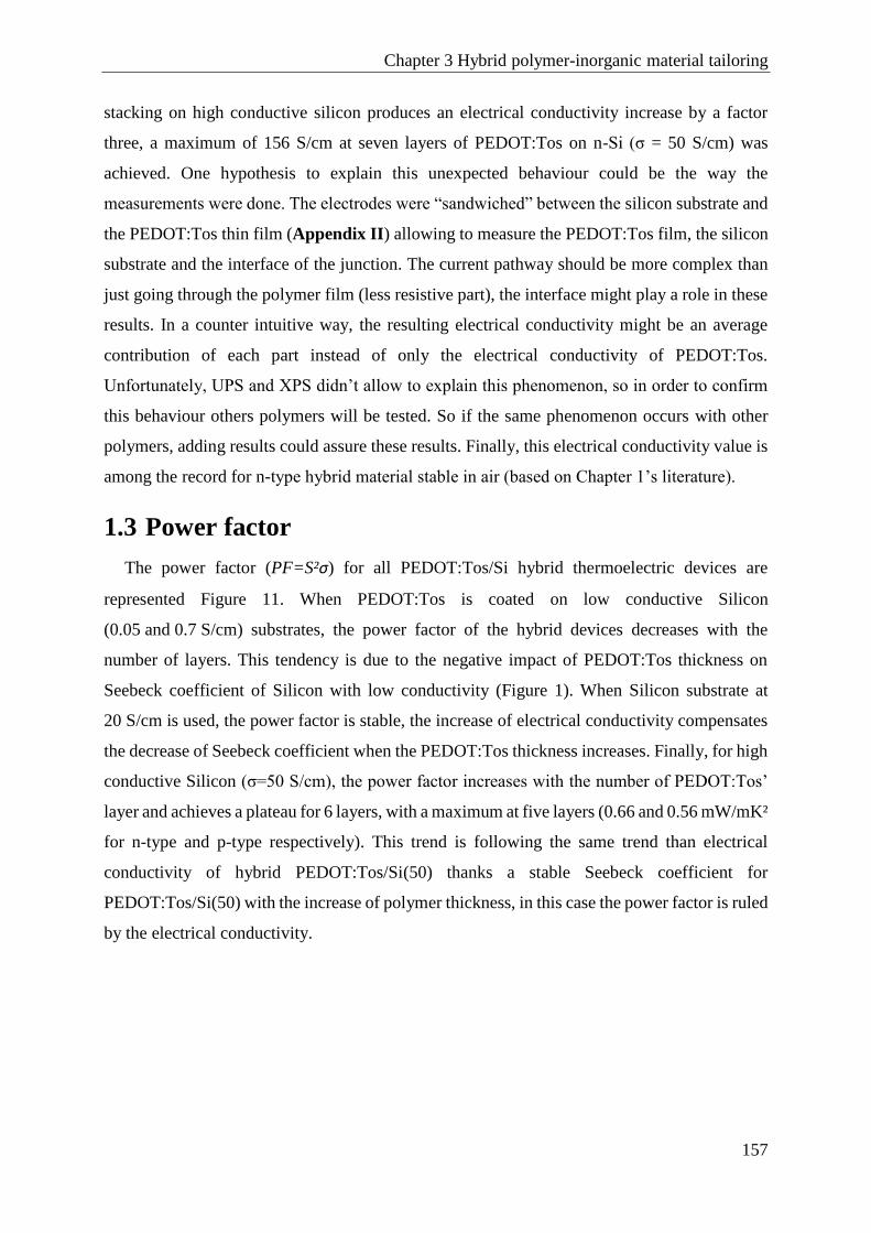
Chapter 3 Hybrid polymer-inorganic material tailoring
157
stacking on high conductive silicon produces an electrical conductivity increase by a factor
three, a maximum of 156 S/cm at seven layers of PEDOT:Tos on n-Si (σ = 50 S/cm) was
achieved. One hypothesis to explain this unexpected behaviour could be the way the
measurements were done. The electrodes were “sandwiched” between the silicon substrate and
the PEDOT:Tos thin film (Appendix II) allowing to measure the PEDOT:Tos film, the silicon
substrate and the interface of the junction. The current pathway should be more complex than
just going through the polymer film (less resistive part), the interface might play a role in these
results. In a counter intuitive way, the resulting electrical conductivity might be an average
contribution of each part instead of only the electrical conductivity of PEDOT:Tos.
Unfortunately, UPS and XPS didn’t allow to explain this phenomenon, so in order to confirm
this behaviour others polymers will be tested. So if the same phenomenon occurs with other
polymers, adding results could assure these results. Finally, this electrical conductivity value is
among the record for n-type hybrid material stable in air (based on Chapter 1’s literature).
1.3 Power factor
The power factor (PF=S²σ) for all PEDOT:Tos/Si hybrid thermoelectric devices are
represented Figure 11. When PEDOT:Tos is coated on low conductive Silicon
(0.05 and 0.7 S/cm) substrates, the power factor of the hybrid devices decreases with the
number of layers. This tendency is due to the negative impact of PEDOT:Tos thickness on
Seebeck coefficient of Silicon with low conductivity (Figure 1). When Silicon substrate at
20 S/cm is used, the power factor is stable, the increase of electrical conductivity compensates
the decrease of Seebeck coefficient when the PEDOT:Tos thickness increases. Finally, for high
conductive Silicon (σ=50 S/cm), the power factor increases with the number of PEDOT:Tos’
layer and achieves a plateau for 6 layers, with a maximum at five layers (0.66 and 0.56 mW/mK²
for n-type and p-type respectively). This trend is following the same trend than electrical
conductivity of hybrid PEDOT:Tos/Si(50) thanks a stable Seebeck coefficient for
PEDOT:Tos/Si(50) with the increase of polymer thickness, in this case the power factor is ruled
by the electrical conductivity.
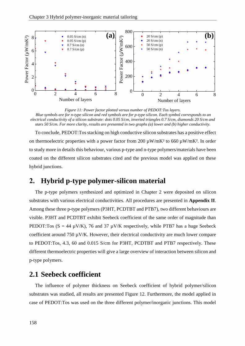
Chapter 3 Hybrid polymer-inorganic material tailoring
158
To conclude, PEDOT:Tos stacking on high conductive silicon substrates has a positive effect
on thermoelectric properties with a power factor from 200 µW/mK² to 660 µW/mK². In order
to study more in details this behaviour, various p-type and n-type polymers/materials have been
coated on the different silicon substrates cited and the previous model was applied on these
hybrid junctions.
Hybrid p-type polymer-silicon material
The p-type polymers synthesized and optimized in Chapter 2 were deposited on silicon
substrates with various electrical conductivities. All procedures are presented in Appendix II.
Among these three p-type polymers (P3HT, PCDTBT and PTB7), two different behaviours are
visible. P3HT and PCDTBT exhibit Seebeck coefficient of the same order of magnitude than
PEDOT:Tos (S = 44 µV/K), 76 and 37 µV/K respectively, while PTB7 has a huge Seebeck
coefficient around 750 µV/K. However, their electrical conductivity are much lower compare
to PEDOT:Tos, 4.3, 60 and 0.015 S/cm for P3HT, PCDTBT and PTB7 respectively. These
different thermoelectric properties will give a large overview of interaction between silicon and
p-type polymers.
2.1 Seebeck coefficient
The influence of polymer thickness on Seebeck coefficient of hybrid polymer/silicon
substrates was studied, all results are presented Figure 12. Furthermore, the model applied in
case of PEDOT:Tos was used on the three different polymer/inorganic junctions. This model
0 2 4 6 80
2
4
6
8 0.05 S/cm (n)
0.05 S/cm (p)
0.7 S/cm (n)
0.7 S/cm (p)
P
ow
er F
acto
r (µ
W/m
K²)
Number of layers0 2 4 6 8
0
200
400
600
800 20 S/cm (p)
20 S/cm (n)
50 S/cm (p)
50 S/cm (n)
Pow
er F
acto
r (µ
W/m
K²)
Number of layers
(a) (b)
Figure 11: Power factor plotted versus number of PEDOT:Tos layers.
Blue symbols are for n-type silicon and red symbols are for p-type silicon. Each symbol corresponds to an
electrical conductivity of a silicon substrate: dots 0.05 S/cm, inverted triangles 0.7 S/cm, diamonds 20 S/cm and
stars 50 S/cm. For more clarity, results are presented in two graphs (a) lower and (b) higher conductivity.

Chapter 3 Hybrid polymer-inorganic material tailoring
159
takes into account the Seebeck coefficient of each material and their electrical conductivity
weighted by their thickness, the expression is rewritten below:
𝑆𝐽𝑢𝑛𝑐𝑡𝑖𝑜𝑛 = 𝑆𝑆𝑖 .1 +
𝑆𝑝𝑜𝑙 . 𝜎𝑝𝑜𝑙.𝑡𝑝𝑜𝑙
𝑆𝑆𝑖. 𝜎𝑆𝑖 . 𝑡𝑆𝑖
1 + 𝜎𝑝𝑜𝑙 .𝑡𝑝𝑜𝑙
𝜎𝑆𝑖. 𝑡𝑆𝑖
(1)
In Figure 12, “dots” are experimental data and “dashed line” are the fitting data calculated
from the model (Equation 1). In case of P3HT (Figure 12a) and PCDTBT (Figure 12b), the
experimental data fit well with the model for hybrid samples on high conductive silicon. In
contrast, a small gap is visible for hybrid sample with low conductive silicon. This phenomenon
was also observed for PEDOT:Tos and was attributed to the model center symmetry to the axis
x=0 instead of Seebeck coefficient value. In fact, experimentally, when the polymer thickness
increases Seebeck coefficient values tend to polymer Seebeck coefficient value. Another
difference with the PEDOT:Tos occurs for the silicon σ= 20 S/cm which has its Seebeck
coefficient less affected by the polymer thickness. The difference in electrical conductivity
between the PEDOT:Tos and the two others polymers should explain it.
In case of PTB7, the model is satisfactory. The polymer thickness does not have any effect
on the Seebeck coefficient value of the hybrid material (Figure 12c). The main reason isn’t only
its high Seebeck coefficient, in fact with a low electrical conductivity, the contribution of the
polymer is largely minimized. This could be explained by the model which takes into account
both thermoelectric properties with respect of the thickness of each material. So the polymer
low conductivity and thickness are “cancelled” compared to silicon thickness and electrical
conductivity (three order of magnitude).
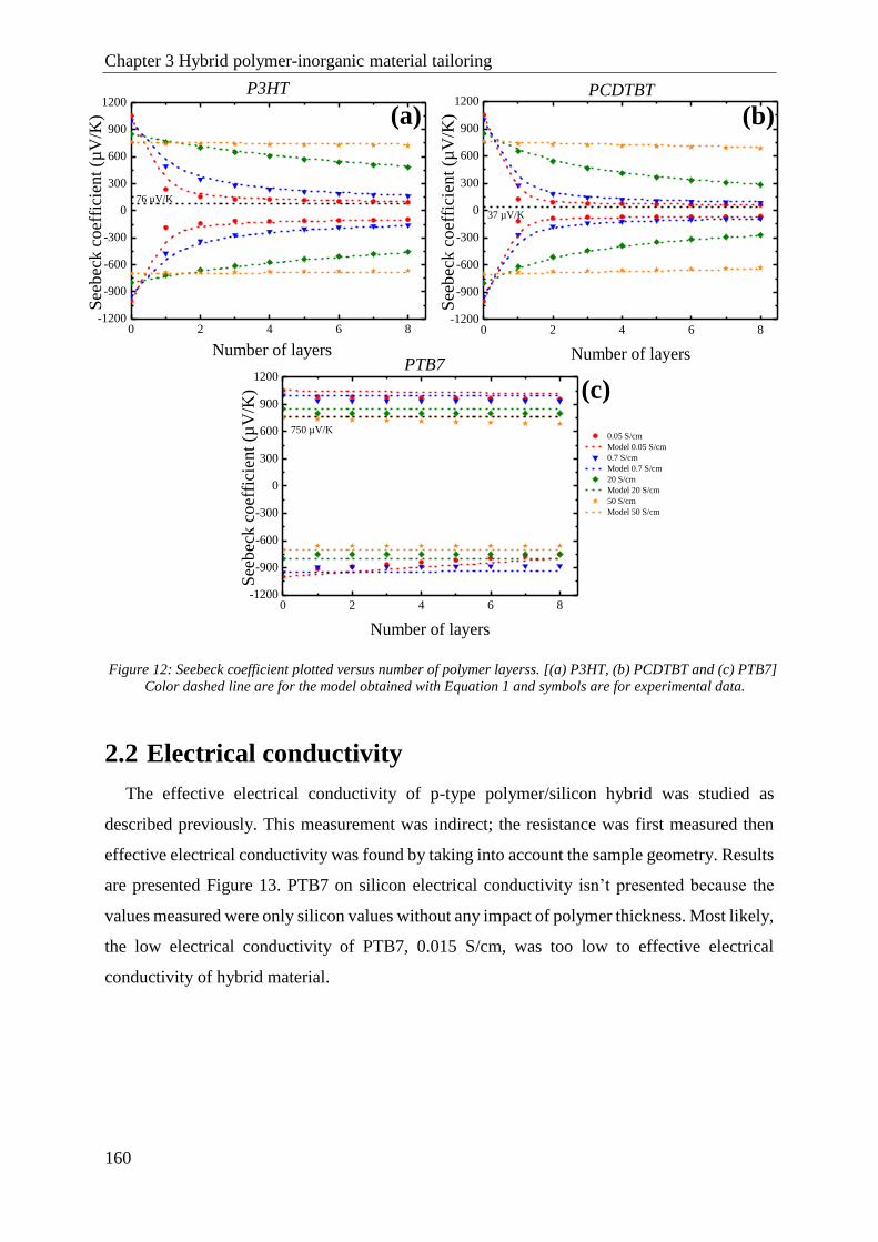
Chapter 3 Hybrid polymer-inorganic material tailoring
160
2.2 Electrical conductivity
The effective electrical conductivity of p-type polymer/silicon hybrid was studied as
described previously. This measurement was indirect; the resistance was first measured then
effective electrical conductivity was found by taking into account the sample geometry. Results
are presented Figure 13. PTB7 on silicon electrical conductivity isn’t presented because the
values measured were only silicon values without any impact of polymer thickness. Most likely,
the low electrical conductivity of PTB7, 0.015 S/cm, was too low to effective electrical
conductivity of hybrid material.
0 2 4 6 8-1200
-900
-600
-300
0
300
600
900
1200
S
eeb
eck
co
effi
cien
t (µ
V/K
)
Number of layers
76 µV/K
0 2 4 6 8-1200
-900
-600
-300
0
300
600
900
1200
See
bec
k c
oef
fici
ent
(µV
/K)
Number of layers
37 µV/K
0 2 4 6 8-1200
-900
-600
-300
0
300
600
900
1200
0.05 S/cm
Model 0.05 S/cm
0.7 S/cm
Model 0.7 S/cm
20 S/cm
Model 20 S/cm
50 S/cm
Model 50 S/cm
See
bec
k c
oef
fici
ent
(µV
/K)
Number of layers
750 µV/K
(a) (b)
(c)
Figure 12: Seebeck coefficient plotted versus number of polymer layerss. [(a) P3HT, (b) PCDTBT and (c) PTB7]
Color dashed line are for the model obtained with Equation 1 and symbols are for experimental data.
P3HT PCDTBT
PTB7

Chapter 3 Hybrid polymer-inorganic material tailoring
161
First, the doping type (positive in red and negative in blue) does not have a high effect on
electrical conductivity values. When the polymer conductivity is lower than electrical
conductivity of silicon, only the silicon value is measured. The results of P3HT with high
conductive silicon aren’t presented because this phenomenon occurs, only electrical
conductivity of silicon was probed like in PTB7 case. However, when polymer conductivity is
higher than substrate one, polymer thickness has an interesting impact on electrical conductivity
of hybrid material. An increase of the value is notable in each cases for P3HT and PCDTBT
(even for low conductive silicon substrate with PCDTBT, the scale bar being to large). This
phenomenon was also observed for PEDOT:Tos, the previous hypothesis of the impact of the
measurement manner should be confirmed with these experimental data. Finally, the electrical
conductivity value of these hybrid materials are a bit higher than bare materials alone.
2.3 Power factor
The power factor (PF=S²σ) for P3HT and PCDTBT /Si hybrid thermoelectric devices are
presented Figure 14. For more visibility, power factor of each polymer were speared in two
graphs, one with low conductive silicon (P3HT (a) and PCDTBT (c)) and the other with high
conductive silicon substrate (P3HT (b) and PCDTBT (d)). In case of PTB7, polymer thickness
does not have any influence on the power factor such as Seebeck coefficient or electrical
conductivity. In all cases presented below, polymer has a negative impact on the power factor
of the hybrid material. Naturally, when the Seebeck coefficient decreases, the power factor
follows its trend even if the electrical conductivity increase. However, contrast to PEDOT:Tos,
when the Seebeck coefficient remains stable (high conductive silicon substrate), the power
0 2 4 6 80.0
0.2
0.4
0.6
0.8
1.0
1.2
Ju
nct
ion (
S/c
m)
0.05 S/cm (p)
0.05 S/cm (n)
0.7 S/cm (p)
0.7 S/cm (n)
Number of layer
0 2 4 6 80
10
20
30
40
50
60
Ju
nct
ion (
S/c
m)
0.05 S/cm (p)
0.05 S/cm (n)
0.7 S/cm (p)
0.7 S/cm (n)
20 S/cm (p)
20 S/cm (n)
50 S/cm (p)
50S/cm (n)
Number of layer
Figure 13: Electrical condcutivity plotted versus number of polymer layers. [(a) P3HT and (b) PCDTBT].
Blue symbols are for n-type silicon and red symbols are for p-type silicon.
(a) (b) P3HT PCDTBT

Chapter 3 Hybrid polymer-inorganic material tailoring
162
factor stay unchanged or decreased. The small changes of electrical conductivity can’t
compensate the loss of Seebeck coefficient.
To conclude, adding stack of p-type polymer with low conductivity on silicon substrate has
none impact in best cases on the performance of the final device but could have a very negative
impact. These polymers were useful to have a better understanding of the interaction between
polymers and silicon on Seebeck coefficient.
0 2 4 6 80
2
4
6
8
0.05 S/cm (n)
0.05 S/cm (p)
0.7 S/cm (n)
0.7 S/cm (p)
Pow
er F
acto
r (µ
W/m
K²)
Number of layer0 2 4 6 8
0
100
200
300
20 S/cm (n)
20 S/cm (p)
50 S/cm (n)
50 S/cm (p)
Po
wer
Fac
tor
(µW
/mK
²)Number of layer
0 2 4 6 80
2
4
6
8
0.05 S/cm (n)
0.05 S/cm (p)
0.7 S/cm (n)
0.7 S/cm (p)
Po
wer
Fac
tor
(µW
/mK
²)
Number of layer0 2 4 6 8
0
100
200
300
20 S/cm (n)
20 S/cm (p)
50 S/cm (n)
50 S/cm (p)
Pow
er F
acto
r (m
W/m
K²)
Number of layer
(a) (b)
(c) (d)
P3HT
PCDTBT
P3HT
PCDTBT
Figure 14: Power factor plotted versus number of polymer layers. [(a,b) P3HT and (c,d) PCDTBT].
Blue symbols are for n-type silicon and red symbols are for p-type silicon.
µ
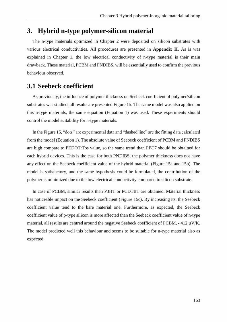
Chapter 3 Hybrid polymer-inorganic material tailoring
163
Hybrid n-type polymer-silicon material
The n-type materials optimized in Chapter 2 were deposited on silicon substrates with
various electrical conductivities. All procedures are presented in Appendix II. As is was
explained in Chapter 1, the low electrical conductivity of n-type material is their main
drawback. These material, PCBM and PNDIBS, will be essentially used to confirm the previous
behaviour observed.
3.1 Seebeck coefficient
As previously, the influence of polymer thickness on Seebeck coefficient of polymer/silicon
substrates was studied, all results are presented Figure 15. The same model was also applied on
this n-type materials, the same equation (Equation 1) was used. These experiments should
control the model suitability for n-type materials.
In the Figure 15, “dots” are experimental data and “dashed line” are the fitting data calculated
from the model (Equation 1). The absolute value of Seebeck coefficient of PCBM and PNDIBS
are high compare to PEDOT:Tos value, so the same trend than PBT7 should be obtained for
each hybrid devices. This is the case for both PNDIBS, the polymer thickness does not have
any effect on the Seebeck coefficient value of the hybrid material (Figure 15a and 15b). The
model is satisfactory, and the same hypothesis could be formulated, the contribution of the
polymer is minimized due to the low electrical conductivity compared to silicon substrate.
In case of PCBM, similar results than P3HT or PCDTBT are obtained. Material thickness
has noticeable impact on the Seebeck coefficient (Figure 15c). By increasing its, the Seebeck
coefficient value tend to the bare material one. Furthermore, as expected, the Seebeck
coefficient value of p-type silicon is more affected than the Seebeck coefficient value of n-type
material, all results are centred around the negative Seebeck coefficient of PCBM, - 412 µV/K.
The model predicted well this behaviour and seems to be suitable for n-type material also as
expected.
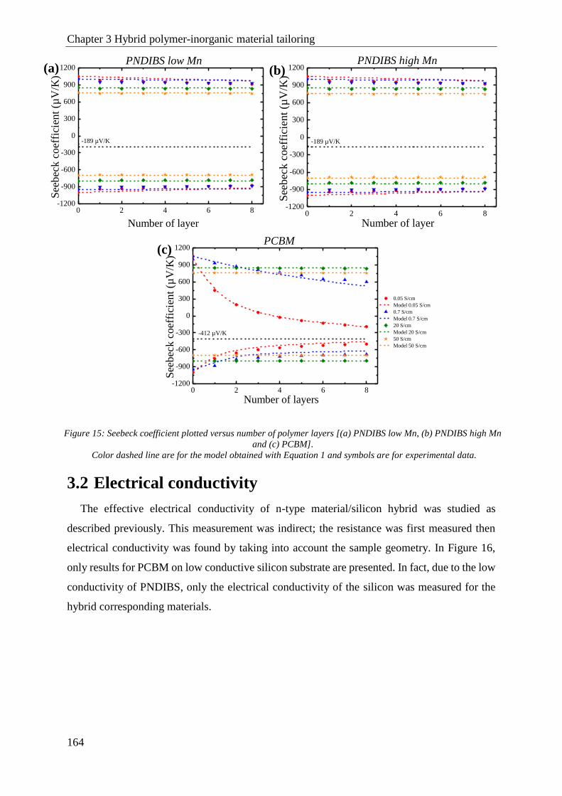
Chapter 3 Hybrid polymer-inorganic material tailoring
164
3.2 Electrical conductivity
The effective electrical conductivity of n-type material/silicon hybrid was studied as
described previously. This measurement was indirect; the resistance was first measured then
electrical conductivity was found by taking into account the sample geometry. In Figure 16,
only results for PCBM on low conductive silicon substrate are presented. In fact, due to the low
conductivity of PNDIBS, only the electrical conductivity of the silicon was measured for the
hybrid corresponding materials.
0 2 4 6 8-1200
-900
-600
-300
0
300
600
900
1200
-412 µV/K
0.05 S/cm
Model 0.05 S/cm
0.7 S/cm
Model 0.7 S/cm
20 S/cm
Model 20 S/cm
50 S/cm
Model 50 S/cm
See
bec
k c
oef
fici
ent
(µV
/K)
Number of layers
0 2 4 6 8-1200
-900
-600
-300
0
300
600
900
1200
S
eeb
eck
co
effi
cien
t (µ
V/K
)
Number of layer
-189 µV/K
0 2 4 6 8-1200
-900
-600
-300
0
300
600
900
1200
-189 µV/K
See
bec
k c
oef
fici
ent
(µV
/K)
Number of layer
(a) (b)
(c)
PNDIBS low Mn PNDIBS high Mn
PCBM
Figure 15: Seebeck coefficient plotted versus number of polymer layers [(a) PNDIBS low Mn, (b) PNDIBS high Mn
and (c) PCBM].
Color dashed line are for the model obtained with Equation 1 and symbols are for experimental data.
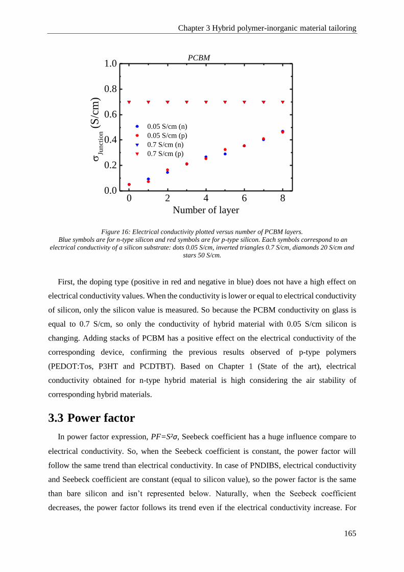
Chapter 3 Hybrid polymer-inorganic material tailoring
165
First, the doping type (positive in red and negative in blue) does not have a high effect on
electrical conductivity values. When the conductivity is lower or equal to electrical conductivity
of silicon, only the silicon value is measured. So because the PCBM conductivity on glass is
equal to 0.7 S/cm, so only the conductivity of hybrid material with 0.05 S/cm silicon is
changing. Adding stacks of PCBM has a positive effect on the electrical conductivity of the
corresponding device, confirming the previous results observed of p-type polymers
(PEDOT:Tos, P3HT and PCDTBT). Based on Chapter 1 (State of the art), electrical
conductivity obtained for n-type hybrid material is high considering the air stability of
corresponding hybrid materials.
3.3 Power factor
In power factor expression, PF=S²σ, Seebeck coefficient has a huge influence compare to
electrical conductivity. So, when the Seebeck coefficient is constant, the power factor will
follow the same trend than electrical conductivity. In case of PNDIBS, electrical conductivity
and Seebeck coefficient are constant (equal to silicon value), so the power factor is the same
than bare silicon and isn’t represented below. Naturally, when the Seebeck coefficient
decreases, the power factor follows its trend even if the electrical conductivity increase. For
0 2 4 6 80.0
0.2
0.4
0.6
0.8
1.0
Ju
nct
ion (
S/c
m)
0.05 S/cm (n)
0.05 S/cm (p)
0.7 S/cm (n)
0.7 S/cm (p)
Number of layer
Figure 16: Electrical conductivity plotted versus number of PCBM layers.
Blue symbols are for n-type silicon and red symbols are for p-type silicon. Each symbols correspond to an
electrical conductivity of a silicon substrate: dots 0.05 S/cm, inverted triangles 0.7 S/cm, diamonds 20 S/cm and
stars 50 S/cm.
PCBM
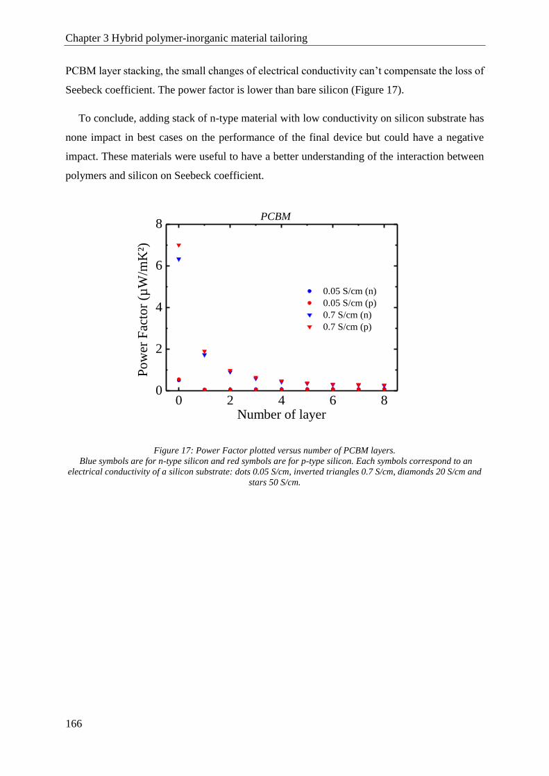
Chapter 3 Hybrid polymer-inorganic material tailoring
166
PCBM layer stacking, the small changes of electrical conductivity can’t compensate the loss of
Seebeck coefficient. The power factor is lower than bare silicon (Figure 17).
To conclude, adding stack of n-type material with low conductivity on silicon substrate has
none impact in best cases on the performance of the final device but could have a negative
impact. These materials were useful to have a better understanding of the interaction between
polymers and silicon on Seebeck coefficient.
0 2 4 6 80
2
4
6
8
0.05 S/cm (n)
0.05 S/cm (p)
0.7 S/cm (n)
0.7 S/cm (p)
Pow
er F
acto
r (µ
W/m
K²)
Number of layer
Figure 17: Power Factor plotted versus number of PCBM layers.
Blue symbols are for n-type silicon and red symbols are for p-type silicon. Each symbols correspond to an
electrical conductivity of a silicon substrate: dots 0.05 S/cm, inverted triangles 0.7 S/cm, diamonds 20 S/cm and
stars 50 S/cm.
PCBM

Chapter 3 Hybrid polymer-inorganic material tailoring
167
D Conclusion
In the present study, the influence of various polymers, p- & n-type, coupled with a large
range of silicon with different doping on thermoelectric properties was examined. It was shown
that the Seebeck coefficient of such hybrid junction can be tuned in magnitude and sign
depending of the silicon and organic material doping and electrical conductivity. These findings
were predicted by a model based on an electric circuit. This model is usable for a large range
of organic material on inorganic substrate. It was also shown that the electrical conductivity,
and so the power factor of bare inorganic material could be increased by adding high conductive
polymers on-top of its. This phenomenon was investigated by UPS and XPS analysis, but none
of these analysis explained well the increase. The main hypothesis found was a huge influence
of the device architecture. In fact, the electrodes were “sandwiched” between the silicon
substrate and the PEDOT:Tos thin film (cf. Appendix II) allowing to measure the polymer
film, the silicon substrate and the interface of the junction. The current pathway should be more
complex than just going through the polymer film (less resistive part), the interface might play
a role in these results. Electrical conductivity and power factor obtained for PEDOT:Tos on
n-type silicon are among the best results described in literature for n-type material stable in the
air. In a later part, this strategy will be adapted to build efficient air stable thermoelectric
generator with n-type and p-type materials based on work done in this Chapter 3.
So in order to elucidate more in details this behaviour, silicon substrate surface will be
modified. Nanowires, pores and pyramids will be made by etching on-top of silicon substrate
allowing to obtain a larger specific area. The interface between the organic material and the
new structured silicon will be different from previously, and its thermoelectric properties will
be studied.

Chapter 3 Hybrid polymer-inorganic material tailoring
168
References
[1] O. Bubnova, X. Crispin, Energy Environ. Sci. 2012, 5, 9345.
[2] M. He, F. Qiu, Z. Lin, Energy Environ. Sci. 2013, 6, 1352.
[3] L.-D. Zhao, G. Tan, S. Hao, J. He, Y. Pei, H. Chi, H. Wang, S. Gong, H. Xu, V. P.
Dravid, C. Uher, G. J. Snyder, C. Wolverton, M. G. Kanatzidis, Science 2016, 351,
141.
[4] C.-Y. Yang, W.-L. Jin, J. Wang, Y.-F. Ding, S. Nong, K. Shi, Y. Lu, Y.-Z. Dai, F.-D.
Zhuang, T. Lei, C.-A. Di, D. Zhu, J.-Y. Wang, J. Pei, Adv. Mater. 2018, 30, 1802850.
[5] B. Russ, M. J. Robb, F. G. Brunetti, P. L. Miller, E. E. Perry, S. N. Patel, V. Ho, W.
B. Chang, J. J. Urban, M. L. Chabinyc, C. J. Hawker, R. A. Segalman, Adv. Mater.
2014, 26, 3473.
[6] G-H. Kim, L. Shao, K. Zhang, K. P. Pipe, Nature Materials, 2013, 12, 719-723.
[7] O. Bubnova, M. Berggren, X. Crispin, J. Am. Chem. Soc. 2012, 134, 16456.
[8] Z. U. Khan, O. Bubnova, M. J. Jafari, R. Brooke, X. Liu, R. Gabrielsson, T. Ederth,
D. R. Evans, J. W. Andreasen, M. Fahlman, X. Crispin, J. Mater. Chem. C 2015, 3,
10616.
[9] O. Bubnova et al., Nature Materials, 2014, 13, 190-194.
[10] K. Shi, F. Zhang, C.-A. Di, T.-W. Yan, Y. Zou, X. Zhou, D. Zhu, J.-Y. Wang, J. Pei,
J. Am. Chem. Soc. 2015, 137, 6979.
[11] Y. Sun, P. Sheng, C. Di, F. Jiao, W. Xu, D. Qiu, D. Zhu, Adv. Mater. 2012, 24, 932.
[12] N. E. Coates et al., Advance Materials, 2013, 25 (11), 1629-1633.
[13] S. K. Yee, N. E. Coates, A. Majumdar, J. J. Urban, R. A. Segalman, Phys. Chem.
Chem. Phys. 2013, 15, 4024.
[14] B. Dörling et al., Advance Materials, 2016, 28 (14), 2782-2789.
[15] R. M. Ireland et al., Advanced Materials, 2015, 2 (6), 1500015.
[16] C. L. Choy, Polymer 1977, 18, 984.
[17] S. M. Haque, J. A. A. Rey, A. AbubakarMasúd, Y. Umar, R. Albarracin, Prop. Appl.
Polym. Dielectr. 2017, http://dx.doi.org/10.5772/67091.
[18] C. J. M. Lasance, 2006, The Seebeck Coefficient., view on https://www.electronics-
cooling.com/2006/11/the-seebeck-coefficient/ (July, 2019).
[19] L. Venema, Nature 2011, 479, 309.
[20] B. V. Zeghbroeck, 2011, Principle of Semiconductor devices: 2.9 Mobility - Resistivity
- Sheet resistance, Colorado, view on ecee.colorado.edu/~bart/book/mobility.htm
(July, 2019).
[21] J. Zhou, B. Liao, B. Qiu, S. Huberman, K. Esfarjani, M. S. Dresselhaus, G. Chen, Proc.
Natl. Acad. Sci. 2015, 112, 14777.
[22] J. Tang, H.-T. Wang, D. H. Lee, M. Fardy, Z. Huo, T. P. Russell, P. Yang, Nano Lett.
2010, 10, 4279.
[23] A. Yamamoto, K. Ogawa, T. Takeuchi, Mater. Trans. 2011, 52, 1539.
[24] A. W. Van Herwaarden, Sens. Actuators 1984, 6, 245.
[25] K. Ding et al., J. Mater. Chem., 2017, 5, 285-291.
[26] Gerald Burns, Solid State Physics, Academic Press, "1st Edition", 1985, 755 (ISBN:
97814832886).
[27] P. Atkins, J. de Paula, Chimie Physique, Bruxelles de Boeck supérieur DL, "4th
Edition", 2013, (ISBD: 978-2-8041-6651-9br)

Chapter 3 Hybrid polymer-inorganic material tailoring
169
[28] C. Goupil, Continuum Theory and Modeling of Thermoelectric Elements, Wiley-VCH
Verlag GmbH & Co. KGaA: Weinheim, Germany, 2016, 360 (ISBN: 978-3-527-
41337-9).
[29] J. P. Joule, The London, Edinburgh, and Dublin Philosophical Magazine and Journal
of Science, 1844, 19 (124), 260-277.
[30] H. Crepin, 2015, Tableau émissivités en thermographie, view on
http://www.thethermograpiclibrary.org/index.php?title=Tableau_%C3%A9missivit%
C3%A9s_en_thermographie (July, 2019).
[31] Y. Singh, Int. J. Mod. Phys. Conf. Ser. 2013, 22, 745.
[32] M. Weis et al., Applied Physics Letters, 2010, 97 (26), 263304.

170

Chapter 4 Silicon nano-structuration
171
Chapter 4
Silicon nano-structuration:
Interface influence on thermoelectric
properties

Chapter 4 Silicon nano-structuration
172
As described previously, silicon has various advantages such as a high abundant earth
reserves, a low cost and a matured manufacturing technology for mass production [1,2].
Unfortunately, nowadays silicon isn’t used in thermoelectric devices due to its high thermal
conductivity and low ZT = 0.01 [3–6]. Nano-structured silicon has recently attracted the attention
of scientist in sensors [7] and photovoltaic cells [8] due to their small cross-sectional area,
large surface-to-volume ratio, and attractive transport properties. During the past years, nano-
structured silicon has also been considered as high potential thermoelectric material with a high
figure of merit ZT value. The main reason was their ability to reduce the thermal conductivity,
while retaining others thermoelectric characteristics [9]. In fact, in silicon the thermal energy is
transported mostly by the lattice vibration rather than by electrons and holes, but in case of
nano-structured silicon, thermal conductivity is decreased by phonon scattering by defects at
the nano-structure surface [10,11]. In this study, the large surface-to-volume ratio
of nano- structured silicon has been used to show the influence of silicon surface area on
thermoelectric properties of hybrid PEDOT:Tos-silicon devices, thus three different structures
with various specific area were made : porous, pyramids and nanowires.
A Silicon nanowires
Theory and principle
Silicon nanowires are one of the most successful examples of nanostructured silicon in
thermoelectricity. Boukai et al. reported a high ZT ~1 at ambient temperature for a single
nanowire device [12]. Thermoelectric properties, Seebeck coefficient and electrical conductivity,
decreased a bit while thermal conductivity has been reduced to 1.6 W/mK. More recently, a
large range of doped silicon nanowire were characterized for thermoelectric application. In both
cases, silicon nanowires showed great potential for future thermoelectric application [13,14].
For device applications, a controllable fabrication of silicon nanostructure is mandatory, in
fact their properties strongly depend on their preparation methods [15,16]. Low-cost and scalable
production of silicon nanowires is essential to their application. Two major low-cost strategies
were developed to fabricate silicon nanostructures, top-down and bottom-up approach. The
most famous method for bottom-up approach is the silicon wire growth via vapour-liquid-solid
(VLS) mechanism via chemical vapour deposition (CVD) developed by Wagner et al. [17].This
method is based on an assembly process joining silicon atoms to form silicon nanowires by
using gold as metallic catalyst, and SiH4 or SiCl4 as gaseous silicon precursors. Concisely, the

Chapter 4 Silicon nano-structuration
173
VLS approach involves the following steps as show Figure 1: (1) formation of liquid
metal- silicon alloy droplets on substrate; (2) dissolution and diffusion of gaseous silicon
precursor into the alloy droplets; and (3) silicon precipitation and axial crystal growth due to
super-saturation and nucleation at the liquid/solid interface.
In case of top-down approach, the most attractive method is the metal-catalyzed
electrodeless etching (MCEE), recently called metal-asssited chemical etching process
(MACE) developed by Ohmi et al. and upgraded by Bohn and co. [18,19]. MACE is a simple and
low-cost method for fabricating silicon nanowires with the ability to control diameter, length
and cross-sectional shape. Furthermore, all procedures could be accomplished in a chemical
laboratory without expensive equipment. In MACE, a silicon substrate is partly covered by a
noble metal (e.g. Au, Pt) and put in an etching solution composed of fluorhydric acid (HF) and
an oxidative agent generally hydrogen peroxide (H2O2). The silicon under the noble metal is
etched faster than the silicon without noble metal coverage, so the noble metals sinks into the
silicon substrate, generating pores forming nanowires. In fact, the etching rate of silicon in an
etching solution without metal is as low as 0.2-0.6 nm/min against 1.5 µm/min when a metal is
used as catalyst [20,21]. For the mechanism, this is well-accepted that the chemical reaction occurs
preferentially near the noble metal, various possible electrochemical reactions have been
proposed to describe the MACE process.
Figure 1: Schematic of silicon nanowires growth steps using VLS method via CVD method.

Chapter 4 Silicon nano-structuration
174
The oxidant, H2O2, is reduced at the metal via a cathode reaction (Equation 1):
H2O2(l) + 2H+ 2H2O(l) + 2h+ (1)
In addition to Equation 1, a reduction of protons into hydrogen via another cathode reaction
was proposed by Harade et al. [22] (Equation 2):
2H+ H2(g) ↑ + 2h+ (2)
At the anode, the silicon substrate is oxidized and dissolved, various models exist for this
dissolution process (anode reaction). These models could be classified in three main groups
(RI, RII and RIII):
(RI) Direct dissolution of silicon in tetravalent state (Equation 3 & 4)
Si(s) + 4h+ + 4HF(l) SiF4(g) + 4H++ (3)
SiF4(g) + 2HF(l) H2SiF6(s) (4)
(RII) Direct dissolution of silicon in divalent state (Equation 5)
Si(s) + 4HF2-(l) SiF6
-(l) + 2HF(l) + H2(g) ↑ + 2e- (5)
(RIII) silicon oxide formation followed by dissolution of oxide (Equation 6 & 7)
Si(s) + 2H2O(l) SiO2(s) + 4H+ + 4e- (6)

Chapter 4 Silicon nano-structuration
175
SiO2(s) + 6HF(l) H2SiF6(l) + 2H2O(l) (7)
However, due to the difficulty of in-situ exploration for the surface state, this is impossible
to predict a more favourable model to describe the mechanism, so Chartier et al. proposed a
well-accepted mixed reaction for the dissolution of silicon in MACE (Equation 8) [19]:
Si(s) + 6HF(l) + nH+ H2SiF6(l) + nh+ + (4-n / 2) H2(g) ↑ (8)
And the overall reaction is (Equation 9):
Si(s) + n/2 H2O2(l) + 6HF(l) nH2O(l) + H2SiF6(l) + (4-n / 2) H2(g) ↑ (9)
Furthermore in order, to totally understand MACE process mechanism, charge transfer has
to be considered for the oxidation and dissolution of silicon. In fact, the noble metal acts as a
microscopic cathode on which the reduction of the oxidant occurs (cathode reaction). The
generated holes are then injected into the silicon substrate in contact with the noble metal. So,
the silicon atoms under the noble metal are oxidized due to the hole injection and dissolved by
HF (anode reaction).
Based on the most accepted mechanism for the MACE process, all steps are described on
Figure 2: (1) The oxidant is reduced at the surface of the noble metal due to the catalytic activity
of the noble metal on the reduction of the oxidant. (2) The holes generated via the reduction of
the oxidant diffuse through the noble metal and are injected into the silicon that is in contact
with the noble metal. (3) The silicon is oxidized by the injected holes and dissolved at the
Si/metal interface by HF. The reactant (HF) and the by-products diffuse along the interface
between the Si and the noble metal. (4) The concentration of holes has its maximum at the
Si/metal interface. Therefore, the Si that is in contact with the metal is etched much faster by
HF than a bare Si surface without metal coverage would be. (5) The holes diffuse from the Si
under the noble metal to off-metal areas or to the wall of the pore if the rate of hole consumption
at the Si/metal interface is smaller than the rate of hole injection. Accordingly, the off-metal
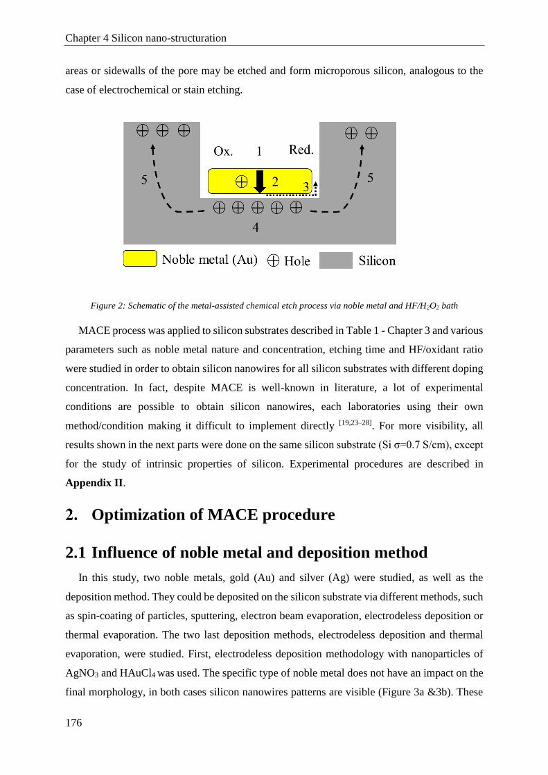
Chapter 4 Silicon nano-structuration
176
areas or sidewalls of the pore may be etched and form microporous silicon, analogous to the
case of electrochemical or stain etching.
Figure 2: Schematic of the metal-assisted chemical etch process via noble metal and HF/H2O2 bath
MACE process was applied to silicon substrates described in Table 1 - Chapter 3 and various
parameters such as noble metal nature and concentration, etching time and HF/oxidant ratio
were studied in order to obtain silicon nanowires for all silicon substrates with different doping
concentration. In fact, despite MACE is well-known in literature, a lot of experimental
conditions are possible to obtain silicon nanowires, each laboratories using their own
method/condition making it difficult to implement directly [19,23–28]. For more visibility, all
results shown in the next parts were done on the same silicon substrate (Si σ=0.7 S/cm), except
for the study of intrinsic properties of silicon. Experimental procedures are described in
Appendix II.
Optimization of MACE procedure
2.1 Influence of noble metal and deposition method
In this study, two noble metals, gold (Au) and silver (Ag) were studied, as well as the
deposition method. They could be deposited on the silicon substrate via different methods, such
as spin-coating of particles, sputtering, electron beam evaporation, electrodeless deposition or
thermal evaporation. The two last deposition methods, electrodeless deposition and thermal
evaporation, were studied. First, electrodeless deposition methodology with nanoparticles of
AgNO3 and HAuCl4 was used. The specific type of noble metal does not have an impact on the
final morphology, in both cases silicon nanowires patterns are visible (Figure 3a &3b). These

Chapter 4 Silicon nano-structuration
177
results mean that the catalytic activity of the noble metal, in case of Au and Ag nanoparticles,
does not have an influence on the etching rate and so on resulting nanostructures.
Then metal, Ag and Au, was deposited by thermal evaporation, a physical deposition method
in vaccum (PVD), different metal thickness was tested and results are presented Figure 4. In
both cases, thickness has an influence on the final silicon nano-structuration, but depending on
the metal type, the final nano-structure is different. A layer of Ag film with a nominal thickness
of 5 nm led to porous structure, and by increasing this nominal thickness, the pore size increases
to form silicon nanowires at 20 nm of Ag thickness (Figure 4a, c, e). For a layer of Au film, the
same behaviour is observed for 5 and 10 nm but when the thickness increases to 20 nm, pores
are bigger but they do not form silicon nanowires (Figure 4b, d, f). So the morphology of the
Ag or Au deposited by thermal evaporation depends on its nominal thickness, it varies with an
increase in nominal thickness from isolated particles to continuous metal film. So the different
morphologies of structures from the etching with metals can be attributed to the different shapes
of distances, and packing manners of the metal particles.
For the rest of the study, despite thermal evaporation allows a more easily morphology
control of the noble metal film, electrodeless deposition was preferred due to its simplicity and
speed to depose noble metal. Finally, Ag nanoparticles was chosen over Au nanoparticles
because they were cheaper and more easily available in the laboratory.
(a) (b)
2µm 2µm
Ag Au
Figure 3: SEM images of Silicon wafers subjected to MACE with (a) silver particles and (b) gold particles

Chapter 4 Silicon nano-structuration
178
2.2 Influence of silver nanoparticles concentration and
etching time
The impact of silver nanoparticles concentration (AgNO3) as well as the etching time in this
solution were studied. The results shown Figure 5 are nanostructures which were formed on the
silver deposited Si samples after etching in aqueous solution containing 5 M HF and 30 wt%
H2O2 (10:1) in 30 mn at room temperature (more details in Appendix II). The concentration of
(a)
2µm
(f)
(d)
(b)
(e)
(c)
2µm
2µm
2µm
2µm
2µm
5 nm 5 nm
10 nm 10 nm
20 nm 20 nm
Figure 4: SEM images of Silicon wafers subjected to MACE with different noble metal thickness.
(a), (c) and (e) are silver particles and (b), (d) and (f) are gold particles for 5,, 10 and 20 nm respectively.

Chapter 4 Silicon nano-structuration
179
AgNO3 in the silver deposition step strongly affects the morphology of the resulting film.
Because Ag does not wet well on the Si surface, islands of Ag are deposited, and by controlling
the AgNO3 solution concentration and immersion time, these islands form “nanoparticles” [29].
First, when the concentration of AgNO3 is less than 0.02M, the silicon nanowires arrays are not
formed (Figure 5a and Figure 5b). This phenomenon is due to the formation mechanisms of
silicon nanostructures in the etching solution (HF/H2O2) after silver deposition step [30]. The
SiO2 or Si underneath the Ag particles is etched away by HF directly, and the Ag particles enter
the pits as they are forming. So, when the Ag particles are small (at low concentration), their
lift-off and Brownian movement may occur during silicon dissolution, resulting in more
disordered silicon nanostructures. The AgNO3 concentration 0.02 and 0.05 M are appropriate
for creating the vertical aligned SiNWs arrays (Figure 5c and Figure 5d). Nevertheless, when
particles concentration increases, the density of nanowires decreases. The reason of this
difference in density is due to a size increase of silver clusters with the concentration on the
surface of silicon. So the size of the areas not covered with silver decreased, and because the
Ag-coated regions of silicon etches faster, SiNWs density decreased.
1µm
1µm 1µm
1µm
(a)
(d)
(b)
0.05M 0.02M
0.01M 0.005M
(c)
Figure 57: SEM images of silicon nanostructures fabricated with (a) 0.005 M, (b) 0.01 M, (c) 0.02 M and (d) 0.05 M
of AgNO3 nanoparticles concentration.

Chapter 4 Silicon nano-structuration
180
Then the influence of time in AgNO3 particles bath on silicon nanostructure was studied.
The AgNO3 concentration was fixed at 0.02 M based on previous results. The same trend as
previously is followed for etching time under 2 mn, none silicon nanowires are formed
(Figure 6a and Figure 6b). The reason is similar than for AgNO3 concentration, the Ag lift-off
and Brownian movement occur during silicon dissolution. Silicon nanowires are formed for
2 mn in the bath, but when the time is increased to 5 or 10 mn, no nanostructure are visible
(Figure 6d and Figure 6e). One of the hypothesis could be that after a long time in silver bath,
“umbrella structures” could be formed, reducing the number of silver nanoparticles achieving
the silicon surface, and so reducing the SiNWs formation [31].
2 µm
(a) 30 s (b) 1 mn
(c) 2 mn (d) 5 mn
(e) 10 mn
2 µm
2 µm
2 µm
2 µm
Figure 6: SEM images of silicon nanostructures fabricated with (a) 30 s, (b) 1 mn, (c) 2 mn, (d) 5 mn and
(e) 10 mn of gold nanoparticles evaporation in PVD machine.

Chapter 4 Silicon nano-structuration
181
2.3 Influence of etching time in HF/H2O2 bath
In this part, the influence of immersion duration in HF/H2O2 bath was studied. The previous
results obtained gave information on which noble metal have to be chosen, the concentration
and immersion time in AgNO3 bath. Experimental procedure details ae given in Appendix II.
Because the influence of HF/H2O2 was well studied by the scientist community and HF/H2O2
volume ratio 10:1 is largely used in MACE procedure, it will be barely discussed here [29,31–34].
When the silicon substrates with Ag nanoparticles are immersed in etching solution
(HF/H2O2), SiO2 is continuously formed form the silicon in contact with Ag nanoparticles with
H2O2 as hole donor and oxidant and dissolved by HF Equation 9). So, H2O2 was chosen as
oxidant due to its low reduction potential versus standard hydrogen electrode (SHE) of 1.76 V
compared to the reduction potential of Ag of -0.81 V versus SHE, favouring transfer of electron
from Ag to H2O2. If the H2O2 concentration increases, the oxidation speed of the silicon around
the Ag nanoparticles increases (more holes injected and so more oxidation occurs), resulting in
the increase of the horizontal etching rate. But in case of high H2O2 concentration, the horizontal
etching speed increases in a higher degree and overcomes the Ag nanoparticle gravity to shift
its position, deviating from the vertical direction, a chaotic porous structure is obtained [33].
Naturally, the immersion time in the etching solution has a significate influence of SiNWs
length as shown Figure 7a, 7b and 7c. The reason is simple, based on the Si etching mechanism,
Si atoms under the silver clusters are oxidised due to the hole injection by H2O2 and dissolved
by HF over the time. So, a longer immersion time of the substrate inside the etching solution
will result in longer Si nanowires.
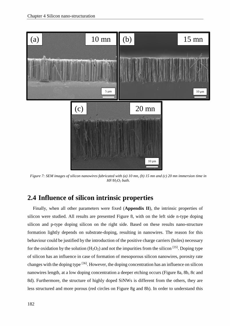
Chapter 4 Silicon nano-structuration
182
2.4 Influence of silicon intrinsic properties
Finally, when all other parameters were fixed (Appendix II), the intrinsic properties of
silicon were studied. All results are presented Figure 8, with on the left side n-type doping
silicon and p-type doping silicon on the right side. Based on these results nano-structure
formation lightly depends on substrate-doping, resulting in nanowires. The reason for this
behaviour could be justified by the introduction of the positive charge carriers (holes) necessary
for the oxidation by the solution (H2O2) and not the impurities from the silicon [35]. Doping type
of silicon has an influence in case of formation of mesoporous silicon nanowires, porosity rate
changes with the doping type [36]. However, the doping concentration has an influence on silicon
nanowires length, at a low doping concentration a deeper etching occurs (Figure 8a, 8b, 8c and
8d). Furthermore, the structure of highly doped SiNWs is different from the others, they are
less structured and more porous (red circles on Figure 8g and 8h). In order to understand this
(a) 10 mn (b) 15 mn
10 µm
(c) 20 mn
10 µm 5 µm
Figure 7: SEM images of silicon nanowires fabricated with (a) 10 mn, (b) 15 mn and (c) 20 mn immersion time in
HF/H2O2 bath.

Chapter 4 Silicon nano-structuration
183
behaviour, various major mechanisms had been proposed, in all of them, a competition between
vertical (SiNWs formation) and horizontal (Porosity in nanowires) etching occurs. First,
dopants act as nucleation sites for pore formation (horizontal etching) during the etching of Si,
so high dopant concentration will lead to more porous and structured SiNWs (hypothesis
supported by Chiappini et al. [37]).
Hochbaum et al. proved that Si followed an electrochemical mechanism during MACE. So
increasing the doping level of the Si results in a decrease of the energy barrier at Si/Ag+
interface, because of the redox potential of Ag+/Ag0 lies below the valence band of Si.
Furthermore, the insulating character of porous Si blocks the transport of holes through porous
layer, instead they proceed by means of the Ag+/Ag0 redox pair diffusing through etched pores
in Si accentuating the formation of pores [38].
On the other hand, Qu et al. proposed a mechanism linked with the dissolution and re-
deposition of Ag [39]. Typically, Ag+ ion cloud is crafted close of Ag particles because of the
oxidation of Ag particles by H2O2. Ag+ quickly reacts with the closest Si near Ag/Si interface
and thus is recovered into Ag particles. So, etching is localized around Ag particles, but because
Ag particles are “trapped in nano-pits created by themselves, vertical etching direction is
preferred. Alongside, H2O2 blocks the recovering of Ag+ into Ag nanoparticles and when the
amount of out-diffusing Ag+ ions reach a certain threshold, these Ag+ ions may start to nucleate
on the sidewall of previously formed Si near weak defective site (e.g., dopants), forming new
Si particles for new pathway, resulting in the pore generation. So highly doped Si will
preferentially form porous silicon nanowires, with the horizontal etching faster than the vertical
one, forming less long nanowires.
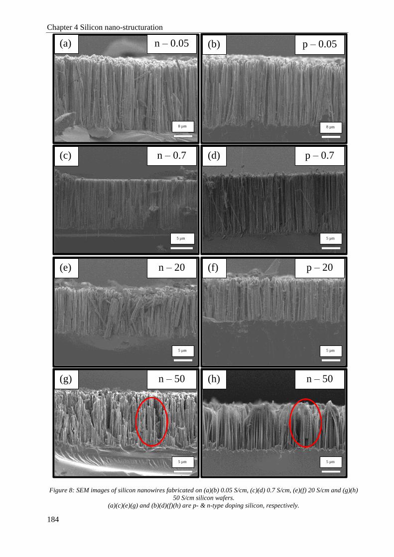
Chapter 4 Silicon nano-structuration
184
Figure 8: SEM images of silicon nanowires fabricated on (a)(b) 0.05 S/cm, (c)(d) 0.7 S/cm, (e)(f) 20 S/cm and (g)(h)
50 S/cm silicon wafers.
(a)(c)(e)(g) and (b)(d)(f)(h) are p- & n-type doping silicon, respectively.
(a) n – 0.05
8 µm
(b) p – 0.05
8 µm
(c) n – 0.7
5 µm
(d) p – 0.7
5 µm
(e) n – 20
5 µm
(f) p – 20
5 µm
(g) n – 50
5 µm
(h) n – 50
5 µm
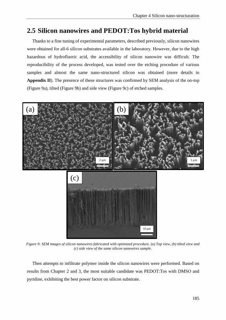
Chapter 4 Silicon nano-structuration
185
2.5 Silicon nanowires and PEDOT:Tos hybrid material
Thanks to a fine tuning of experimental parameters, described previously, silicon nanowires
were obtained for all-6 silicon substrates available in the laboratory. However, due to the high
hazardous of hydrofluoric acid, the accessibility of silicon nanowire was difficult. The
reproducibility of the process developed, was tested over the etching procedure of various
samples and almost the same nano-structured silicon was obtained (more details in
Appendix II). The presence of these structures was confirmed by SEM analysis of the on-top
(Figure 9a), tilted (Figure 9b) and side view (Figure 9c) of etched samples.
Then attempts to infiltrate polymer inside the silicon nanowires were performed. Based on
results from Chapter 2 and 3, the most suitable candidate was PEDOT:Tos with DMSO and
pyridine, exhibiting the best power factor on silicon substrate.
(a)
2 µm
(b)
5 µm
(c)
10 µm
Figure 9: SEM images of silicon nanowires fabricated with optimized procedure. (a) Top view, (b) tilted view and
(c) side view of the same silicon nanowires sample.

Chapter 4 Silicon nano-structuration
186
From an experimental point of view, this kind of packed nanostructures has a main
drawback, a poor wettability. In fact, the top surface of the silicon nanowires is similar to the
nanostructure observed for lotus leaf [40–42]. A so called Lotus effect, superhydophobicity should
occur when PEDOT:Tos will be deposited on top of etched silicon substrate [41]. This
phenomenon was observed during the spin-coating; none polymer was present at the end of the
process. Nevertheless, the origin of this phenomenon could be attributed to an additional
parameter as observed Adachi and Rusli groups [43,44]. In fact, the last treatment before the
polymer deposition has an important role on the surface wettability. As explained more in
details in Appendix II, silicon nanowires were post-treated by HF. This treatment tends to form
more hydrophobic surface. The surface is therefore functionalized by Si-H termination. But
when no post-treatment is made, the last bath of the etching process is a HNO3:H2O mixture.
This “stain etching” role is to functionalize SiNWs by hydrophilic groups. In fact, the surface
of SiNWs is partially oxidized by the HNO3 solution according to the following Equation 10:
2𝑥 HNO3(l) + Si(s) → SiOx(s) + 2𝑥 NO2(g) + 𝑥 H2O(l) (10)
The surface is therefore functionalized by the following groups: Si-O-Si, Si=O, and Si-OH.
Experimental conditions were adapted in order to avoid wettability problems (Appendix II),
and PEDOT:Tos were successfully deposited with this new methodology. In fact, in the last
procedure step, SiNWs were treated with HF to remove the oxide layer. Unfortunately, this last
step made the surface hydrophobic. So, in order to successfully deposited the PEDOT:Tos on
top of SiNWs, this last step wasn’t performed. Furthermore, the solution (monomer with
oxidant) was let 30 s on-top the substrate before spin-coating. SEM images confirmed the well
deposition of PEDOT:Tos between and on-top of the SiNWs Figure 10).

Chapter 4 Silicon nano-structuration
187
Then, PEDOT:Tos layers were stacked on top of various silicon with different
conductivities, and their Seebeck coefficient, electrical conductivity and power factor were
measured in agreement with results of Chapter 3 (Figure 11). All procedures are presented in
Appendix II.
The same behaviour as previously presented in Chapter 3 for hybrid PEDOT:Tos-silicon
devices is clearly visible. In Figure 11a, the Seebeck coefficient decreases rapidly to reach a
plateau value for low conductive silicon (0.05 and 0.7 S/cm). In case of silicon with high
conductivity (20 and 50 S/cm), Seebeck coefficient decreases more slowly when the polymer
thickness increases. The same absolute Seebeck coefficient values are obtained for p- & n-type
substrates with polymer on top.
In case of electrical conductivity, the doping type (positive in red and negative in blue) does
not have a high effect on values regarding the experimental standard deviation (Figure 11b).
But, depending on the Si substrates conductivities, the electrical conductivity values are
(c)
2 µm
(d)
2 µm
(a)
10 µm
(b)
5 µm
Figure 10: SEM images of bare silicon nanowires and with PEDOT:Tos on top.
(a) Side view and (c) Top view of bare silicon nanowires. (b) Side view and (d) Top view of PEDOT:Tos on silicon
nanowires.

Chapter 4 Silicon nano-structuration
188
different. Principally, an increase of polymer thickness induces an increase of the electrical
conductivity until the five PEDOT:Tos layer then a plateau is achieved. Low conductivity
values are obtained for the Silicon with low conductivity and high values for high conductive
Silicon with a maximum at seven layers of PEDOT:Tos. These results are similar to bare silicon
with PEDOT:Tos (Chapter 3).
Finally, power factor followed the same trend than bare silicon with PEDOT:Tos (Figure
11c). When PEDOT:Tos is coated on low conductive Silicon (0.05 and 0.7 S/cm) substrates,
the power factor of the hybrid devices decreases with the number of layers. This tendency is
due to the negative impact of PEDOT:Tos thickness on Seebeck coefficient of Silicon with low
conductivity. When Silicon substrate at 20 S/cm is used, the power factor is stable, the increase
of electrical conductivity compensates the decrease of Seebeck coefficient when the
PEDOT:Tos thickness increases. Finally, for high conductive Silicon (50 S/cm), the power
factor increases with the number of PEDOT:Tos’ layer and achieves a plateau for six layers,
with a maximum at five layers.
0 2 4 6 8
0
50
100
150
200
Ju
nct
ion (
S/c
m)
0,05 S/cm (p)
0,05 S/cm (n)
0,7 S/cm (p)
0,7 S/cm (n)
20 S/cm (p)
20 S/cm (n)
50 S/cm (p)
50 S/cm (n)
Number of layers
0 2 4 6 80
200
400
600
800 0.05 S/cm (p)
0.05 S/cm (n)
0.7 S/cm (p)
0.7 S/cm (n)
20 S/cm (p)
20 S/cm (n)
50 S/cm (p)
50 S/cm (n)
Pow
er F
acto
r (µ
W/m
.K²)
Number of layers
0 2 4 6 8-1200
-900
-600
-300
0
300
600
900
1200
PEDOT:Tos
0.05 S/cm
0.7 S/cm
20 S/cm
50 S/cm
See
bec
k c
oef
fici
ent
(µV
/K)
Number of layers
p-type
n-type
44 µV/K
Figure 11: (a) Seebeck coefficient, (b) Electrical conductivity and (c) Power factor plotted versus number of
PEDOT:Tos layer on SiNWs.
Blue symbols are for n-type silicon and red symbols are for p-type silicon.
(a)
(b) (c)
PEDOT :Tos on SiNWs

Chapter 4 Silicon nano-structuration
189
PEDOT:Tos stacking on SiNWs products the same behaviour than PEDOT:Tos on bare
silicon. In order to see if the nano-structuration of silicon had an effect on thermoelectric
properties, Figure 12 reports a comparison between these two cases. A ratio between
thermoelectric properties (S, σ, and PF) of hybrid material previously described with bare
silicon and SiNWs were done. Full, empty, and half-full symbols represent the Seebeck
coefficient, the electrical conductivity and the power factor ratio between bare silicon and
SiNWs, respectively. Finally, the dashed-line correspond to unchanged thermoelectric
properties.
Etching silicon surface into SiNWs has an important effect on the Seebeck coefficient and
the electrical conductivity (Figure 12a). On average, Seebeck coefficient of SiNWs is 5-10%
higher than Seebeck coefficient of bare silicon. However, the electrical conductivity decreased
by also 5-10 % on average. But, because the contribution of Seebeck coefficient is square, the
power factor increased by a 10-20% factor in case of SiNWs (Figure 12b). The enhancement
of thermoelectric parameters could be due to the reduction in dimensionality on silicon. This
phenomenon was pointed out by pioneers’ group like Dresselhaus and co-workers [45–48], the
Seebeck coefficient increases in monodimensional (nanowires) and/or bidimensional
structures. In fact, the Seebeck coefficient strongly depends on the distribution in energy of
charge carriers, and in particular it increases when the average difference between the
carriers’ energy and the Fermi energy increases. In low dimensional systems, the DoS is reshape
with respect to bulk systems, in such a way that charge carriers are spread to higher energies.
So, an increase in both S and σ should occur. However, as explained by Pennelli and al.,
structures must have a size of few nanometers to obtain a noticeable increase of the Seebeck
coefficient with respect to its bulk value [46], which is the case in this study. Moreover, the
electrical conductivity is strongly reduced by the surface scattering of charge carriers, directly
confirmed by results in Figure 12b.

Chapter 4 Silicon nano-structuration
190
To conclude, SiNWs coupled with PEDOT:Tos results in a better thermoelectric properties
compare to the bare silicon with PEDOT:Tos. A maximum increase of 20% of the power factor
was observed. Unfortunately, the mechanism behind this enhancement was not confirmed by
other analysis. The model developed in Chapter 3 isn’t enough complex to describ well this
new “architecture”. Nakamura developed an atomistic model to predict Seebeck coefficient
value of silicon nanowires on basis of first-principles calculation [49]. He proved fundamental
effect of change in DoS by dimensional reduction to SiNWs, enhancing the thermoelectric
performances. Finally, this is worth to note that the interface between the silicon and the
polymer plays an important role in this hybrid devices.
0 2 4 6 80.8
0.9
1.0
1.1
1.2 0.05 S/cm (n)
0.05 S/cm (p)
0.7 S/cm (n)
0.7 S/cm (p)
20 S/cm (n)
20 S/cm (p)
50 S/cm (n)
50 S/cm(p)
0.05 S/cm (n)
0.05 S/cm (p)
0.7 S/cm (n)
0.7 S/cm (p)
20 S/cm (n)
20 S/cm (p)
50 S/cm (n)
50 S/cm (p)
Si bulk
S
i nan
ow
ires
/ S
i bu
lk
Number of layers
S
0 2 4 6 80.7
0.8
0.9
1.0
1.1
1.2
1.3
0.05 S/cm (p)
0.05 S/cm (n)
0.7 S/cm (p)
0.7 S/cm (n)
20 S/cm (p)
20 S/cm (n)
50 S/cm (p)
50 S/cm (n)
Number of layers
PF
nan
ow
ires / PF
bu
lk
PF
(a) (b)
Figure 12: Comparison between (a) thermoelectric properties and (b) power of factor for bare silicon and
SiNWs with different PEDOT:Tos thickness on top.
Full and empty symbols are for Seebeck coefficient and electrical conductivity, respectively.
Blue symbols are for n-type silicon and red symbols are for p-type silicon.

Chapter 4 Silicon nano-structuration
191
B Porous silicon
Porous silicon (pSi) is a different form of nanostructured silicon. In 1990s, pSi generated
large interest thanks to its photoluminescence properties [50,51]. Research were mainly focused
on the optoelectronic applications, until Canham and Arens-Fischer’s group revealed an
extremely low thermal conductivity for this nanostructure [51,52]. Depending on the fraction of
pores, the thermal conductivity range could be from 0.89 to 0.1 W/mK at room temperature,
three orders of magnitude lower than that of the bulk silicon [52]. This low thermal conductivity
opened the possibility of pSi to thermoelectric applications. Grossman and coll. are among
some groups who studied the potential of pSi as efficient thermoelectric material [53].They found
comparable ZT values between pSi and SiNWs, and they underlined a few possible advantages
over the SiNWs. From a manufacturing point of view, pSi is easier to obtain from bulk silicon.
In addition, this is more straightforward to connect pSi to electrical conductors due to its bulk
nature than an array of SiNWs.
In their report, Föll et al. reported various mechanism for the formation of pores. The pores
size, length and type are really dependant of experimental conditions [54]. In addition, these
physical parameters have also a huge influence on thermoelectric properties, as shown
Martin-Palma et al. in their recent study [55].
In this report, the pSi was obtained as a side-product during the formation of silicon
nanowires. Experimental conditions for the pSi weren’t studied in details, like in SiNWs case
(All experimental conditions for pSi formation are described in Appendix II). Figure 13 shows
the morphology and the size of pores on top of silicon substrate. Based on IUPAC standard [56],
different pores categories could be distinguished by looking at the pore diameter and the
distance between pores. In this case, macropores were obtained, geometries i.e. diameter and
distance, are over 50 nm confirmed by SEM analysis of the on-top surface.
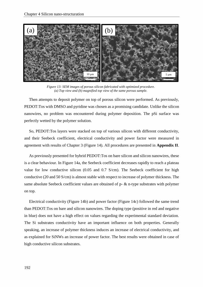
Chapter 4 Silicon nano-structuration
192
Then attempts to deposit polymer on top of porous silicon were performed. As previously,
PEDOT:Tos with DMSO and pyridine was chosen as a promising candidate. Unlike the silicon
nanowires, no problem was encountered during polymer deposition. The pSi surface was
perfectly wetted by the polymer solution.
So, PEDOT:Tos layers were stacked on top of various silicon with different conductivity,
and their Seebeck coefficient, electrical conductivity and power factor were measured in
agreement with results of Chapter 3 (Figure 14). All procedures are presented in Appendix II.
As previously presented for hybrid PEDOT:Tos on bare silicon and silicon nanowires, these
is a clear behaviour. In Figure 14a, the Seebeck coefficient decreases rapidly to reach a plateau
value for low conductive silicon (0.05 and 0.7 S/cm). The Seebeck coefficient for high
conductive (20 and 50 S/cm) is almost stable with respect to increase of polymer thickness. The
same absolute Seebeck coefficient values are obtained of p- & n-type substrates with polymer
on top.
Electrical conductivity (Figure 14b) and power factor (Figure 14c) followed the same trend
than PEDOT:Tos on bare and silicon nanowires. The doping type (positive in red and negative
in blue) does not have a high effect on values regarding the experimental standard deviation.
The Si substrates conductivity have an important influence on both properties. Generally
speaking, an increase of polymer thickness induces an increase of electrical conductivity, and
as explained for SiNWs an increase of power factor. The best results were obtained in case of
high conductive silicon substrates.
(a)
10 µm
(b)
5 µm
Figure 13: SEM images of porous silicon fabricated with optimized procedure.
(a) Top view and (b) magnified top view of the same porous sample.

Chapter 4 Silicon nano-structuration
193
PEDOT:Tos stacking on pSi products the same behaviour than PEDOT:Tos on bare silicon
and SiNWs. Figure 15 shows a comparison between bare and porous silicon substrates covered
by PEDOT:Tos. A ratio between thermoelectric properties (S, σ, and PF) of hybrid material
previously described with bare silicon and pSi were done. Full, empty, and half-full symbols
represent the Seebeck coefficient, the electrical conductivity and the power factor ratio between
bare silicon and pSi, respectively. Finally, the dashed-line correspond to unchanged
thermoelectric properties.
Generally speaking, pores have a lower influence on thermoelectric properties than
nanowires. On average, Seebeck coefficient of pSi is <5% higher than Seebeck coefficient of
bare silicon (5-10 % higher in case of SiNWs) (Figure 15a). The electrical conductivity
decreased also by less than <5% on average (Figure 15a). This decrease is lower in pSi case
0 2 4 6 8-1200
-900
-600
-300
0
300
600
900
1200
PEDOT:Tos
0.05 S/cm
0.7 S/cm
20 S/cm
50 S/cm
See
bec
k c
oef
fici
ent
(µV
/K)
Number of layers
p-type
n-type
44 µV/K
0 2 4 6 80
50
100
150
200
Ju
nct
ion (
S/c
m)
0,05 S/cm (p)
0,05 S/cm (n)
0,7 S/cm (p)
0,7 S/cm (n)
20 S/cm (p)
20 S/cm (n)
50 S/cm (p)
50 S/cm (n)
Number of layers
0 2 4 6 80
200
400
600
800 0.05 S/cm (p)
0.05 S/cm (n)
0.7 S/cm (p)
0.7 S/cm (n)
20 S/cm (p)
20 S/cm (n)
50 S/cm (p)
50 S/cm (n)
Pow
er F
acto
r (µ
W/m
.K²)
Number of layers
PEDOT :Tos on pSi (a)
(b) (c)
Figure 14: (a) Seebeck coefficient, (b) Electrical conductivity and (c) Power factor plotted versus number of
PEDOT:Tos layer on pSi.
Blue symbols are for n-type silicon and red symbols are for p-type silicon.

Chapter 4 Silicon nano-structuration
194
than SiNWs but the resulting power factor isn’t higher in pSi than SiNWs (Figure 12b - 15b).
The reason is the “squared” contribution of Seebeck coefficient in power factor formula.
The small enhancement of thermoelectric properties could also be due to the reduction in
dimensionality on silicon, as previously described for SiNWs [45-48] (more details in SiNWs
section). The decrease of electrical conductivity was due to the difficulty of transporting
electron across the junctions between pores, directly confirmed by results in Figure 15b. This
phenomenon was noticed in various studies on pSi [57–59].
To conclude, pSi coupled with PEDOT:Tos results in a better thermoelectric properties
compare to the bare silicon with PEDOT:Tos. A maximum increase of 10% of the power factor
was observed. Unfortunately, the mechanism behind this enhancement was not confirmed by
other analysis. On the other hand, these results were inferior to results obtained for SiNWs with
PEDOT:Tos, confirming that the interface between the silicon and the polymer plays an
important role in the hybrid devices. Finally, despite lower thermoelectric performances
compare to SiNWs, pSi has the advantage to be tuned by filling the pores with appropriate
materials, and so tune the electronic transport properties.
0 2 4 6 80.8
0.9
1.0
1.1
1.2 0.05 S/cm (p)
0.05 S/cm (n)
0.7 S/cm (p)
0.7 S/cm (n)
20 S/cm (p)
20 S/cm (n)
50 S/cm (p)
50 S/cm (n)
0.05 S/cm(p)
0.05 S/cm (n)
0.7 S/cm (p)
20 S/cm (n)
20 S/cm (p)
50 S/cm (n)
50 S/cm (p)
50 S/cm (n)
Si bulk
Si p
oro
us /
Si b
ulk
Number of layers
S
0 2 4 6 80.7
0.8
0.9
1.0
1.1
1.2
1.3
0.05 S/cm (p)
0.05 S/cm (n)
0.7 S/cm (p)
0.7 S/cm (n)
20 S/cm (p)
20 S/cm (n)
50 S/cm (p)
50 S/cm (n)
Number of layers
PF
po
rou
s / PF
bu
lk
PF
(a) (b)
Figure 158: Comparison between (a) thermoelectric properties and (b) power of factor for bare silicon and pSi
with different PEDOT:Tos thickness on top.
Full and empty symbols are for Seebeck coefficient and electrical conductivity, respectively.
Blue symbols are for n-type silicon and red symbols are for p-type silicon.

Chapter 4 Silicon nano-structuration
195
C Silicon pyramids
Theory and principle
Surface nano-structuration of crystalline silicon wafers is a process used in various fields.
From optoelectronic industry [60] to biological applications [61], silicon wet etching has been
studied and improved in order to address the specific requirements of technological fields
challenges. Depending on the etchant or the crystalline orientation, isotropic or anisotropic
etching could be achieved. Since decades, one of the most famous anisotropic wet etching is
done with potassium hydroxide (KOH) [62]. The mechanism behind the etching process is
described in the Equation 11 below:
Si(s) + 4OH-(l) Si(OH)4(l) + 4e- (11)
In case of <100> silicon, the nanostructure obtained is pyramid structure. The reason is due
to a difference on the (100) and (111) directions since the etching rate on the (111) direction is
lower than (100) direction [63,64]. For the (100) orientation, surface silicon atoms with two
backbonds, connecting to two underlying silicon are present at the surface. The two dangling
groups could make a nucleophilic reaction with OH radical, and so this injection of electrons
will break these bonds and released a silicon-hydroxide complex (Figure 16a). In case of (111)
orient plane, only one dangling bond is present for each surface silicon, thus making it harder
to be etched when comparing with a (100) oriented plane (Figure 16b).
Si
Si
Si
Si
Si
SiSi
2 OH-
OH-
Si
Si
Si
Si
Si
SiSi
OH
OH
OH
2 e-
e-
Figure 169: Etching mechanism of KOH for (a) (100) Silicon and (b) (111) Silicon substrates.
(a)
(b)

Chapter 4 Silicon nano-structuration
196
In addition, different chemicals could be used in order to interact and compete with OH
radicals. Isopropyl alcohol (IPA) is the most used molecule to modulate the etching rate of
specific crystallographic planes in KOH wet etching procedure. IPA acts as a mask, limiting
the access of “KOH particles” to the surface of the silicon sample [65,66]. IPA slows down the
reaction between the silicon surface and the hydroxide ions (OH-) [67]. However, no chemical
reaction seems to be formed between IPA and silicon atoms, thus acting as a mere modulation
agent, rather than an etching stop agent [68].
The control of the pyramid shape in wet etching depends to a precise design of the etching
conditions [69,70]. So, in this report, the influence of potassium hydroxide concentration,
isopropyl alcohol concentration and duration time on texture of monocrystalline silicon wafers
were studied and followed by SEM analysis. For more visibility, all results shown in the next
parts were done on the same silicon substrate (Si σ=0.7 S/cm). Experimental procedures are
described in Appendix II.
1.1 Influence of isopropyl alcohol concentration
In this study, the influence of IPA concentration on silicon surface, during anisotropic
etching process, was studied and followed with SEM analysis. The results shown Figure 17 are
nanostructures which were formed on the Si samples after 25min etching in aqueous solution
containing 20wt% KOH with different concentrations of IPA (3, 5, 7 and 9 wt%) at 80°C (more
details in Appendix II). As described in Equation 11, the silicon wet etching reaction comes
from by-products, silicates. When these silicates aren’t dispersed from the surface of the silicon,
they act as pseudo-masks preventing the continuous etching and promoting a very rough and
heterogeneous etching. Assuring a constant flow between these silicates and fresh OH radicals
allows for a better control of the process, improving both smoothness and homogeneity across
the sample. KOH wet etching was performed inside a large beaker with external temperature
control under magnetic stirring. The magnetic stirring during the etching process increases the
homogeneity, in fact by creating an internal spiral flow, silicates are diluted and a continuous
OH radical could access to the silicon substrate. Then the temperature was set at 80 °C to give
energy to the system to accelerate the etching process.
As shown in Figure 17, IPA concentration has an important influence on number and
morphology of pyramids on top of treated silicon surface. From 3 to 7 wt%, the pyramids
completely cover the entire surface, only the size of pyramids changed. At 9 wt%, this is clearly
visible that the surface isn’t totally covered by pyramids. In fact, the density of the formed

Chapter 4 Silicon nano-structuration
197
pyramids is limited by the etching reaction rate. At high reactions rates, the density of pyramids
covering the surface is reduced, and lead to the breaking of the hydrogen bonding network by
the collected alcohol. So, silicates and isopropyl alcohol formed a near surface layer that hinders
the formation of any more pyramids [71]. A concentration of 5 wt% of IPA was chosen for the
rest of this study, offering a perfect balance between surface covering and pyramids size.
1.2 Influence of potassium hydroxide concentration
KOH concentration was changed from 15 to 30 wt% in order to study its influence on silicon
surface. SEM analysis was used to follow the top structural change of the silicon surface, all
results are presented in Figure 18. Si samples were etched 25 min with 5wt% of IPA at 80 °C.
The shape and the surface coverage of the pyramids clearly depend on the concentration of the
KOH concentration. At 15 wt%, all the surface is covered but the shape of the pyramids isn’t
well defined, the amount of KOH should not be enough to completely form pyramids
(Figure 18a). Then, at 20wt%, all the surface is also covered by pyramids and their shape are
(a) 3 wt%
10 µm
(b) 5 wt%
(c) 7 wt% (d) 9 wt%
10 µm
10 µm 10 µm
Figure 17: SEM images of silicon nanostructures fabricated with (a) 3, (b) 5, (c) 7 and (d) 9 wt% of IPA.

Chapter 4 Silicon nano-structuration
198
more uniform and sharp compare to 15 wt% of KOH (Figure 18b). But when the concentration
is increased, as shown Figure 18c and Figure 18d, the etching rate decreased and the pyramids
became smaller and did not fully fill the surface. This phenomenon could be explained by the
fact that the dissolution kinetics are altered with the high removal of silicon atoms from the
crystalline surface. This hinders the silicates formation, and the high silicon dissolution rate is
not keep up. The concentrations of the silicates complexes are also increasing, and as see
previously, they acted as a protective layer near the silicon surface, preventing the etchants from
accessing the surface [71]. A concentration of 20 wt% of KOH was chosen for the rest of this
study, offering a perfect balance between surface covering and pyramids size.
(
(a) 15 wt%
10 µm
(b) 20 wt%
10 µm
(c) 25 wt%
10 µm
(d) 30 wt%
10 µm
Figure 18: SEM images of silicon nanostructures fabricated with (a) 15, (b) 20, (c) 25 and (d) 30 wt% of KOH.

Chapter 4 Silicon nano-structuration
199
1.3 Influence of etching time
In this part, the influence of immersion duration in KOH/IPA bath at 80°C was studied. The
results shown in Figure 19 are pyramids which were formed on the Si samples etched in aqueous
solution containing 20 wt% of KOH and 5 wt% of IPA at different immersion time, from 15 to
30 min, at 80°C. This is obviously visible that etching time affects the silicon surface. At an
etching time of 15 min, small pyramid patterns distributed in patches with empty regions
between them are observed. These smooth empty areas could be attributed to the relatively short
etching time, pyramids did not have time to be formed. At higher etching time, the surface is
totally covered by pyramids. Increasing the etching time at this point plays only on pyramids
size and distribution. Until 25 min, the pyramids are more uniform, and after the pyramids start
to be less uniform and sharp. This problem could be related to a long immersion in the bath, in
fact pyramids become attacked by the KOH which became less selective between the bare
silicon surface and the pyramid surface. This result, shown in Figure 19d, is in agreement with
this theory, the sharpness of the pyramids is lost in favour of heterogeneous surface on top of
its.
(c) 25 min
10 µm
(a) 15 min
10 µm
(b) 20 min
10 µm
(d) 30 min
10 µm
Figure 19: SEM images of silicon pyrramids fabricated with (a) 15 mn, (b) 20 mn, (c) 25 mn and (d) 30 mn
immersion time in KOH/IPA bath.
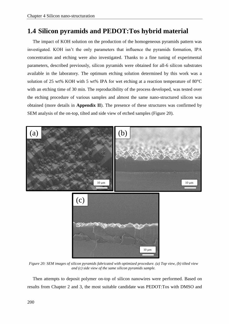
Chapter 4 Silicon nano-structuration
200
1.4 Silicon pyramids and PEDOT:Tos hybrid material
The impact of KOH solution on the production of the homogeneous pyramids pattern was
investigated. KOH isn’t the only parameters that influence the pyramids formation, IPA
concentration and etching were also investigated. Thanks to a fine tuning of experimental
parameters, described previously, silicon pyramids were obtained for all-6 silicon substrates
available in the laboratory. The optimum etching solution determined by this work was a
solution of 25 wt% KOH with 5 wt% IPA for wet etching at a reaction temperature of 80°C
with an etching time of 30 min. The reproducibility of the process developed, was tested over
the etching procedure of various samples and almost the same nano-structured silicon was
obtained (more details in Appendix II). The presence of these structures was confirmed by
SEM analysis of the on-top, tilted and side view of etched samples (Figure 20).
Then attempts to deposit polymer on-top of silicon nanowires were performed. Based on
results from Chapter 2 and 3, the most suitable candidate was PEDOT:Tos with DMSO and
(a)
10 µm
(b)
10 µm
(c)
10 µm
Figure 20: SEM images of silicon pyramids fabricated with optimized procedure. (a) Top view, (b) tilted view
and (c) side view of the same silicon pyramids sample.
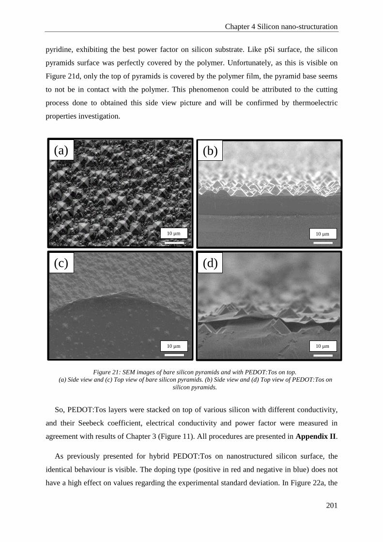
Chapter 4 Silicon nano-structuration
201
pyridine, exhibiting the best power factor on silicon substrate. Like pSi surface, the silicon
pyramids surface was perfectly covered by the polymer. Unfortunately, as this is visible on
Figure 21d, only the top of pyramids is covered by the polymer film, the pyramid base seems
to not be in contact with the polymer. This phenomenon could be attributed to the cutting
process done to obtained this side view picture and will be confirmed by thermoelectric
properties investigation.
So, PEDOT:Tos layers were stacked on top of various silicon with different conductivity,
and their Seebeck coefficient, electrical conductivity and power factor were measured in
agreement with results of Chapter 3 (Figure 11). All procedures are presented in Appendix II.
As previously presented for hybrid PEDOT:Tos on nanostructured silicon surface, the
identical behaviour is visible. The doping type (positive in red and negative in blue) does not
have a high effect on values regarding the experimental standard deviation. In Figure 22a, the
(a)
10 µm
(b)
10 µm
(c)
10 µm
(d)
10 µm
Figure 21: SEM images of bare silicon pyramids and with PEDOT:Tos on top.
(a) Side view and (c) Top view of bare silicon pyramids. (b) Side view and (d) Top view of PEDOT:Tos on
silicon pyramids.
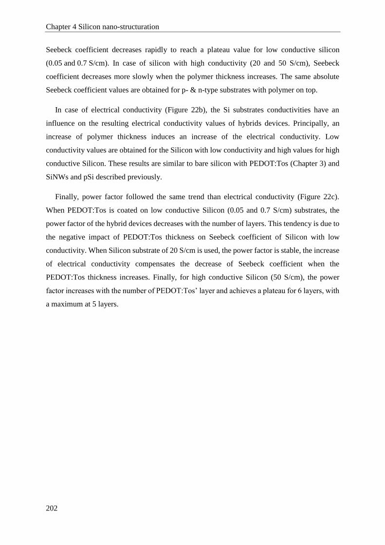
Chapter 4 Silicon nano-structuration
202
Seebeck coefficient decreases rapidly to reach a plateau value for low conductive silicon
(0.05 and 0.7 S/cm). In case of silicon with high conductivity (20 and 50 S/cm), Seebeck
coefficient decreases more slowly when the polymer thickness increases. The same absolute
Seebeck coefficient values are obtained for p- & n-type substrates with polymer on top.
In case of electrical conductivity (Figure 22b), the Si substrates conductivities have an
influence on the resulting electrical conductivity values of hybrids devices. Principally, an
increase of polymer thickness induces an increase of the electrical conductivity. Low
conductivity values are obtained for the Silicon with low conductivity and high values for high
conductive Silicon. These results are similar to bare silicon with PEDOT:Tos (Chapter 3) and
SiNWs and pSi described previously.
Finally, power factor followed the same trend than electrical conductivity (Figure 22c).
When PEDOT:Tos is coated on low conductive Silicon (0.05 and 0.7 S/cm) substrates, the
power factor of the hybrid devices decreases with the number of layers. This tendency is due to
the negative impact of PEDOT:Tos thickness on Seebeck coefficient of Silicon with low
conductivity. When Silicon substrate of 20 S/cm is used, the power factor is stable, the increase
of electrical conductivity compensates the decrease of Seebeck coefficient when the
PEDOT:Tos thickness increases. Finally, for high conductive Silicon (50 S/cm), the power
factor increases with the number of PEDOT:Tos’ layer and achieves a plateau for 6 layers, with
a maximum at 5 layers.

Chapter 4 Silicon nano-structuration
203
PEDOT:Tos stacking on silicon pyramids products a different behaviour than PEDOT:Tos
on SiNWs or pSi. The behaviour is near to PEDOT:Tos on bare silicon. So, in order to compare
the thermoelectric properties of bare and pyramids silicon, Figure 23 shows a comparison
between these two cases. A ratio between thermoelectric properties (S, σ, and PF) of hybrid
material previously described with bare silicon and Si pyramids was done. Full, empty, and
half-full symbols represent the Seebeck coefficient, the electrical conductivity and the power
factor ratios between bare silicon and Si pyramids, respectively. Finally, the dashed-line
correspond to unchanged thermoelectric properties.
Generally speaking, pyramids have a low influence on thermoelectric properties. On
average, Seebeck coefficient and electrical conductivity of Si pyramids are comparable to
thermoelectric properties of the bare silicon (Figure 23a). In some cases, a negative influence
0 2 4 6 8-1200
-900
-600
-300
0
300
600
900
1200
PEDOT:Tos
0.05 S/cm
0.7 S/cm
20 S/cm
50 S/cm
See
bec
k c
oef
fici
ent
(µV
/K)
Number of layers
p-type
n-type
44 µV/K
0 2 4 6 80
50
100
150
200 0,05 S/cm (p)
0,05 S/cm (n)
0,7 S/cm (p)
0,7 S/cm (n)
20 S/cm (p)
20 S/cm (n)
50 S/cm (p)
50 S/cm (n)
Ju
nct
ion (
S/c
m)
Number of layers0 2 4 6 8
0
200
400
600
800 0.05 S/cm (p)
0.05 S/cm (n)
0.7 S/cm (p)
0.7 S/cm (n)
20 S/cm (p)
20 S/cm (n)
50 S/cm (p)
50 S/cm (n)
Pow
er F
acto
r (µ
W/m
.K²)
Number of layers
PEDOT :Tos on Silicon pyramids (a)
(b) (c)
Figure 22: (a) Seebeck coefficient, (b) Electrical conductivity and (c) Power factor plotted versus number of
PEDOT:Tos layer on Si pyramids.
Blue symbols are for n-type silicon and red symbols are for p-type silicon.
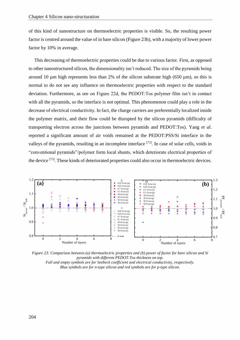
Chapter 4 Silicon nano-structuration
204
of this kind of nanostructure on thermoelectric properties is visible. So, the resulting power
factor is centred around the value of in bare silicon (Figure 23b), with a majority of lower power
factor by 10% in average.
This decreasing of thermoelectric properties could be due to various factor. First, as opposed
to other nanostructured silicon, the dimensionality isn’t reduced. The size of the pyramids being
around 10 µm high represents less than 2% of the silicon substrate high (650 µm), so this is
normal to do not see any influence on thermoelectric properties with respect to the standard
deviation. Furthermore, as see on Figure 22d, the PEDOT:Tos polymer film isn’t in contact
with all the pyramids, so the interface is not optimal. This phenomenon could play a role in the
decrease of electrical conductivity. In fact, the charge carriers are preferentially localized inside
the polymer matrix, and their flow could be disrupted by the silicon pyramids (difficulty of
transporting electron across the junctions between pyramids and PEDOT:Tos). Yang et al.
reported a significant amount of air voids remained at the PEDOT:PSS/Si interface in the
valleys of the pyramids, resulting in an incomplete interface [72]. In case of solar cells, voids in
“conventional pyramids”/polymer form local shunts, which deteriorate electrical properties of
the device [73]. These kinds of deteriorated properties could also occur in thermoelectric devices.
0 2 4 6 80.8
0.9
1.0
1.1
1.2 0.05 S/cm (p)
0.05 S/cm (n)
0.7 S/cm (p)
0.7 S/cm (n)
20 S/cm (p)
20 S/cm (n)
50 S/cm (p)
50 S/cm (n)
0.05 S/cm (p)
0.05 S/cm (n)
0.7 S/cm (p)
0.7 S/cm (n)
20 S/cm (p)
20 S/cm (n)
50 S/cm (p)
50 S/cm (n)
Si bulk
Si p
oro
us /
Si b
ulk
Number of layers
S
0 2 4 6 80.7
0.8
0.9
1.0
1.1
1.2
1.3 0.05 S/cm (n)
0.05 S/cm (p)
0.7 S/cm (n)
0.7 S/cm (p)
20 S/cm (n)
20 S/cm (p)
50 S/cm (n)
50 S/cm (p)
Number of layers
PF
py
ramid
s / PF
bu
lk
PF(a) (b)
Figure 23: Comparison between (a) thermoelectric properties and (b) power of factor for bare silicon and Si
pyramids with different PEDOT:Tos thickness on top.
Full and empty symbols are for Seebeck coefficient and electrical conductivity, respectively.
Blue symbols are for n-type silicon and red symbols are for p-type silicon.

Chapter 4 Silicon nano-structuration
205
To conclude, silicon pyramids coupled with PEDOT:Tos results in a lower thermoelectric
properties compare to the bare silicon with PEDOT:Tos. Unfortunately, this kind of
“conventional pyramids” aren’t adapted to the polymer deposition. In their study, Yang et al.
developed inverted pyramids, and showed a better covering of the nanostructured silicon [72].
The formation of inverted pyramids is simple, the etching process occurs via copper-
nanoparticles in HF/H2O2 bath, this interesting methodology was not applied in this work [74].

Chapter 4 Silicon nano-structuration
206
D Conclusion
Through various etching procedures, three different silicon nanostructures were obtained. A
fine tuning of these etching parameters allowed to make reproducible nanowires, pores and
pyramids on top of silicon substrates. The best polymer developed in Chapter 2, PEDOT:Tos
with DMSO and pyridine, was deposited on the nanostructured silicon. All etching procedures
and polymer deposition were followed with SEM analysis.
Then the thermoelectric properties of all three hybrid nanostructured silicon with
PEDOT:Tos on top devices were compared to the devices made in Chapter 3, bare silicon with
the same polymer. Porous silicon and silicon nanowires showed the best power factor
enhancement compare to bare silicon. Thanks to a decreasing of the dimensionality, a higher
Seebeck coefficient was obtained, and despite a decreasing of the electrical conductivity, the
power factor was increased by a 10 to 20 % factor in best cases. Unfortunately, conventional
pyramids didn’t show the same behaviour, in fact due to a low covering of polymer on top of
silicon surface, a decreasing of power factor was noticed.
Finally, the interface between the polymer and the nanostructured silicon shown an
important effect. By increasing the specific surface, hybrid devices provided very high power
factor (Figure 24) and this should result in efficient thermoelectric generator, described in
Chapter 5. Some improvements, about the silicon nanostructuration, are provided in
perspectives section such as the formation of inverted pyramids covered by nanowires (the
resulting specific area should be the maximum obtainable) [75].
0 2 4 6 80
200
400
600
800 NWs (p)
NWs (n)
Pores (p)
Pores (n)
Pyramids (p)
Pyramids (n)
Po
wer
Fac
tor
(µW
/m.K
²)
Number of layers
Figure 24: Influence of different silicon nanostructure on Power factor of hybrid PEDOT:Tos-Silicon (σ=50S/cm).
Vertical lines, empty dots and pyramids correspond to nanowires, pores and pyramids nanostructures respectively.
Blue symbols are for n-type silicon and red symbols are for p-type silicon.

Chapter 4 Silicon nano-structuration
207
References
[1] L. E. Bell, Science 2008, 321, 1457.
[2] K. Yazawa, A. Shakouri, Environ. Sci. Technol. 2011, 45, 7548.
[3] S. LeBlanc, S. K. Yee, M. L. Scullin, C. Dames, K. E. Goodson, Renew. Sustain.
Energy Rev. 2014, 32, 313.
[4] B. M. Curtin, E. A. Codecido, S. Krämer, J. E. Bowers, Nano Lett. 2013, 13, 5503.
[5] J. Tang, H.-T. Wang, D. H. Lee, M. Fardy, Z. Huo, T. P. Russell, P. Yang, Nano Lett.
2010, 10, 4279.
[6] L. Weber, E. Gmelin, Appl. Phys. A 1991, 53, 136.
[7] K. Kim, C. Park, D. Kwon, D. Kim, M. Meyyappan, S. Jeon, J.-S. Lee, Biosens.
Bioelectron. 2016, 77, 695.
[8] E. Garnett, P. Yang, Nano Lett. 2010, 10, 1082.
[9] A. I. Hochbaum, R. Chen, R. D. Delgado, W. Liang, E. C. Garnett, M. Najarian, A.
Majumdar, P. Yang, Nature 2008, 451, 163.
[10] D. Li, Y. Wu, R. Fan, P. Yang, A. Majumdar, Appl. Phys. Lett. 2003, 83, 3186.
[11] J. Lee, W. Lee, J. Lim, Y. Yu, Q. Kong, J. J. Urban, P. Yang, Nano Lett. 2016, 16,
4133.
[12] A. I. Boukai, Y. Bunimovich, J. Tahir-Kheli, J.-K. Yu, W. A. Goddard Iii, J. R. Heath,
Nature 2008, 451, 168.
[13] E. Krali, Z. A. K. Durrani, Appl. Phys. Lett. 2013, 102, 143102.
[14] J. Kim, Y. Hyun, Y. Park, W. Choi, S. Kim, H. Jeon, T. Zyung, M. Jang, J. Nanosci.
Nanotechnol. 2013, 13, 6416.
[15] V. Schmidt, J. V. Wittemann, S. Senz, U. Gösele, Adv. Mater. 2009, 21, 2681.
[16] X. Duan, C. M. Lieber, J. Am. Chem. Soc. 2000, 122, 188.
[17] R. S. Wagner, W. C. Ellis, Appl. Phys. Lett. 1964, 4, 89.
[18] Proceedings of the Fourth International Symposium on Cleaning Technology in
Semiconductor Device Manufacturing; Novak, R. E.; Rużyłło, J.; Electrochemical
Society, Eds.; Proceedings; Electrochemical Society: Pennington, NJ, 1996.
[19] C. Chartier, S. Bastide, C. Lévy-Clément, Electrochimica Acta 2008, 53, 5509.
[20] K. Choi, Y. Song, I. Oh, J. Oh, RSC Adv. 2015, 5, 76128.
[21] C. Gondek, M. Lippold, I. Röver, K. Bohmhammel, E. Kroke, J. Phys. Chem. C 2014,
118, 2044.
[22] Y. Harada, X. Li, P. W. Bohn, R. G. Nuzzo, J. Am. Chem. Soc. 2001, 123, 8709.
[23] M.-L. Zhang, K.-Q. Peng, X. Fan, J.-S. Jie, R.-Q. Zhang, S.-T. Lee, N.-B. Wong, J.
Phys. Chem. C 2008, 112, 4444.
[24] S. K. Srivastava, D. Kumar, S. W. Schmitt, K. N. Sood, S. H. Christiansen, P. K. Singh,
Nanotechnology 2014, 25, 175601.
[25] K.-Q. Peng, X. Wang, L. Li, Y. Hu, S.-T. Lee, Nano Today 2013, 8, 75.
[26] K. A. Gonchar, L. A. Osminkina, R. A. Galkin, M. B. Gongalsky, V. S. Marshov, V.
Yu. Timoshenko, M. N. Kulmas, V. V. Solovyev, A. A. Kudryavtsev, V. A. Sivakov,
J. Nanoelectron. Optoelectron. 2012, 7, 602.
[27] S. Gielis, M. V. der Veen, S. D. Gendt, P. M. Vereecken, ECS Trans. 2011, 33, 49.
[28] L. U. Vinzons, L. Shu, S. Yip, C.-Y. Wong, L. L. H. Chan, J. C. Ho, Nanoscale Res.
Lett. 2017, 12, 385.
[29] J. Kumar, S. Ingole, J. Electron. Mater. 2018, 47, 1583.
[30] K. Q. Peng, J. J. Hu, Y. J. Yan, Y. Wu, H. Fang, Y. Xu, S. T. Lee, J. Zhu, Adv. Funct.
Mater. 2006, 16, 387.

Chapter 4 Silicon nano-structuration
208
[31] S. Li, W. Ma, Y. Zhou, X. Chen, Y. Xiao, M. Ma, W. Zhu, F. Wei, Nanoscale Res.
Lett. 2014, 9, 196.
[32] F. Toor, J. B. Miller, L. M. Davidson, L. Nichols, W. Duan, M. P. Jura, J. Yim, J.
Forziati, M. R. Black, Nanotechnology 2016, 27, 412003.
[33] Y. Liu, G. Ji, J. Wang, X. Liang, Z. Zuo, Y. Shi, Nanoscale Res. Lett. 2012, 7, 663.
[34] H. Omar, A. M. Md. Jani, M. Rusop, S. Abdullah, AIP Conf. Proc. 2016, 1733,
020016.
[35] C. Chiappini, In Handbook of Porous Silicon; Canham, L., Ed.; Springer International
Publishing: Cham, 2014; pp. 171–186.
[36] W. McSweeney, O. Lotty, N. V. V. Mogili, C. Glynn, H. Geaney, D. Tanner, J. D.
Holmes, C. O’Dwyer, J. Appl. Phys. 2013, 114, 034309.
[37] C. Chiappini, X. Liu, J. R. Fakhoury, M. Ferrari, Adv. Funct. Mater. 2010, 20, 2231.
[38] A. I. Hochbaum, D. Gargas, Y. J. Hwang, P. Yang, Nano Lett. 2009, 9, 3550.
[39] Y. Qu, L. Liao, Y. Li, H. Zhang, Y. Huang, X. Duan, Nano Lett. 2009, 9, 4539.
[40] H. J. Ensikat, P. Ditsche-Kuru, C. Neinhuis, W. Barthlott, Beilstein J. Nanotechnol.
2011, 2, 152.
[41] A. Marmur, Langmuir 2004, 20, 3517.
[42] W. Barthlott, In Klima- und Umweltforschung an der Universität Bonn; 1992; pp. 117–
120.
[43] A. S. Togonal, L. He, P. Roca i Cabarrocas, Rusli, Langmuir 2014, 30, 10290.
[44] Y. Kato, S. Adachi, J. Electrochem. Soc. 2011, 158, K157.
[45] G. Liang, W. Huang, C. S. Koong, J.-S. Wang, J. Lan, J. Appl. Phys. 2010, 107,
014317.
[46] G. Pennelli, M. Macucci, J. Appl. Phys. 2013, 114, 214507.
[47] L. D. Hicks, M. S. Dresselhaus, Phys. Rev. B 1993, 47, 16631.
[48] L. D. Hicks, M. S. Dresselhaus, Phys. Rev. B 1993, 47, 12727.
[49] K. Nakamura, Jpn. J. Appl. Phys. 2017, 56, 06GH04.
[50] L. T. Canham, W. Y. Leong, M. I. J. Beale, T. I. Cox, L. Taylor, Appl. Phys. Lett.
1992, 61, 2563.
[51] A. G. Cullis, L. T. Canham, P. D. J. Calcott, J. Appl. Phys. 1997, 82, 909.
[52] G. Gesele, J. Linsmeier, V. Drach, J. Fricke, R. Arens-Fischer, J. Phys. Appl. Phys.
1997, 30, 2911.
[53] J.-H. Lee, G. A. Galli, J. C. Grossman, Nano Lett. 2008, 8, 3750.
[54] H. Föll, M. Christophersen, J. Carstensen, G. Hasse, Mater. Sci. Eng. R Rep. 2002, 39,
93.
[55] R. J. Martín-Palma, H. Cabrera, B. Martín-Adrados, D. Korte, E. Pérez-Cappe, Y.
Mosqueda, M. A. Frutis, E. Danguillecourt, Mater. Res. Express 2018, 5, 015004.
[56] IUPAC, (2019), Databases - IUPAC Int. Union Pure Appl. Chem, view on
https://iupac.org/what-we-do/databases/ (July, 2019).
[57] M. Bouaïcha, M. Khardani, B. Bessaïs, Mater. Sci. Eng. B 2008, 147, 235.
[58] P. V. More, S. Jeong, J.-Y. Lee, Y.-H. Seo, B.-H. Ryu, Y. Choi, J. Mater. Chem. 2012,
22, 23553.
[59] Z. H. Khan, Appl. Surf. Sci. 2009, 255, 8874.
[60] U. Gangopadhyay, K. Kim, S. K. Dhungel, P. K. Basu, J. Yi, Renew. Energy 2006, 31,
1906.
[61] S. Indermun, R. Luttge, Y. E. Choonara, P. Kumar, L. C. du Toit, G. Modi, V. Pillay,
J. Control. Release Off. J. Control. Release Soc. 2014, 185, 130.
[62] H. Seidel, L. Csepregi, A. Heuberger, H. Baumgärtel, J. Electrochem. Soc. 1990, 137,
3612.

Chapter 4 Silicon nano-structuration
209
[63] K. C. Vernon, T. J. Davis, F. H. Scholes, D. E. Gómez, D. Lau, J. Raman Spectrosc.
2010, 41, 1106.
[64] D. Kim, J. Korean Phys. Soc. 2009, 55, 1767.
[65] I. Zubel, M. Kramkowska, Sens. Actuators Phys. 2004, 115, 549.
[66] K. P. Rola, I. Zubel, Microsyst. Technol. 2013, 19, 635.
[67] H. Park, S. Kwon, J. S. Lee, H. J. Lim, S. Yoon, D. Kim, Sol. Energy Mater. Sol. Cells
2009, 93, 1773.
[68] E. D. Palik, H. F. Gray, P. B. Klein, J. Electrochem. Soc. 1983, 130, 956.
[69] Weihua Han, Xiang Yang, Ying Wang, Fuhua Yang, Jinzhong Yu, In 2008 5th IEEE
International Conference on Group IV Photonics; 2008; pp. 146–148.
[70] C. Trompoukis, I. Abdo, R. Cariou, I. Cosme, W. Chen, O. Deparis, A. Dmitriev, E.
Drouard, M. Foldyna, E. G.- Caurel, I. Gordon, B. Heidari, A. Herman, L. Lalouat,
K.-D. Lee, J. Liu, K. Lodewijks, F. Mandorlo, I. Massiot, A. Mayer, V. Mijkovic, J.
Muller, R. Orobtchouk, G. Poulain, P. Prod’Homme, P. R. i Cabarrocas, C. Seassal, J.
Poortmans, R. Mertens, O. E. Daif, V. Depauw, Phys. Status Solidi A 2015, 212, 140.
[71] A. M. Al-Husseini, B. Lahlouh, Bull. Mater. Sci. 2019, 42.
[72] L. Yang, Y. Liu, W. Chen, Y. Wang, H. Liang, Z. Mei, A. Kuznetsov, X. Du, ACS
Appl. Mater. Interfaces 2016, 8, 26.
[73] T.-G. Chen, B.-Y. Huang, E.-C. Chen, P. Yu, H.-F. Meng, Appl. Phys. Lett. 2012, 101,
033301.
[74] Y. Wang, L. Yang, Y. Liu, Z. Mei, W. Chen, J. Li, H. Liang, A. Kuznetsov, D.
Xiaolong, Sci. Rep. 2015, 5, 10843.
[75] H.-Y. Chen, H.-L. Lu, Q.-H. Ren, Y. Zhang, X.-F. Yang, S.-J. Ding, D. W. Zhang,
Nanoscale 2015, 7, 15142.

210

Chapter 5 Thermoelectric generator
211
Chapter 5
Thermoelectric generator:
Novel hybrid organic-inorganic approach

Chapter 5 Thermoelectric generator
212
In our modern society, electricity production is a global issue. Another important topic is the
waste of heat (energy), especially during the electricity production. Coupled to recent
environmental considerations, thermoelectric generators (TEGs) modules should be a part of
the solution. A typical TEG is composed of thermoelectric materials couples (p- & n-type
materials) connected together electrically in series and thermally in parallel, converting a part
of the thermal energy passing through them into electricity. TEGs allow to obtain a direct
energy conversion without any moving parts nor working fluids inside. However, their low
efficiency compared to others energy-conversion technologies, due to the low performance of
thermoelectric material, is an issue (Figure 1) [1].
Actually in the market, most TEGs are fabricated from inorganic materials, and can reach
ZT>1 at room temperature [2]. Inorganic thermoelectric generators could be classified as
function of their application fields:
o Electricity generation in extreme environments: historically space exploration was a
springboard for thermoelectricity, with thermal generator based on nuclear technology.
This system is called radioisotope thermoelectric generators (RTGs). The natural
disintegration of radioactive atoms releasing heat that is converted in electricity [3,4].
o Waste heat harvesting: all energy-conversion system has not perfect yield, losses are
present and mostly thermal. The most attractive sector for TEGs is the automobile sector
Figure 1: Thermoelectrics in the global landscape of energy conversion. The efficiency comparison of
thermoelectrics and other energy-conversion technologies as a function of the heat-source temperature. The
ZT values are assumed to be temperature independent, and the heat-sink temperature is set at room
temperature.

Chapter 5 Thermoelectric generator
213
where 40% of the gasoline combustion is break down as exhaust gas and heat [5].
Nowadays, this technology is no longer an idea but became real. Famous automobile
constructors, Ford or BMW, developed TEGs prototypes with high power output around
few hundreds of watts [6]. Aircraft and ships are also fields where TEGs are studied [7,8].
o Decentralized domestic power: in developed countries, an estimated 1.2 billion – 17%
of the global population – do not have access to the electricity grid. Biomass is the main
energy source. Different societies and scientist groups started the marketing of small
combustion stoves with efficient combustion [9–11].
o Micro-generation for microelectronics: Recent advances in microelectronics have led to
the rapid emergence and development of micro-actuators and intelligent wireless
sensors in the industry. Today, these devices can work with only a few hundred
milliwatts. Industrialists are therefore looking for micro-generator producing a few
milliwatts to supply and make these micro-instruments stand alone. In industrial
environments, heat sources are very numerous: hot fluid pipes, furnaces, steam pipes,
motors, air conditioning, heating, bearings ... TEGs are therefore a prime candidate for
this challenge. Low maintenance and good behavior in difficult environments are
important assets for TEGs. For example, Micropelt MPG-D751 modules with sizes of
3.3x4.2x1.1 mm3 can produce more than 1 mW for a temperature difference of 10 °C
and more than 10mW for a difference of 30 °C [12].
o Solar TEG: Thermally, the most abundant source is undoubtedly the sun, which could
be consider as a source of heat for a TEG. The main problem of this technology is the
low thermal flux (around 103 W/m² on average), which requires the establishment of a
flux concentration system to achieve satisfactory yields. McEnaney et al. developed a
solar thermoelectric generator giving 10% efficiency based on a geometric optical
concentration ratio of 45.
Despite their dominant presence in previous cited fields, inorganic TEGs have some
drawbacks [13]. The main drawback is the low abundance of inorganic elements in Earth’s crust
and in oceans. For example, the most used inorganic material in TEGs, Bi2Te3, is composed of
two rarest “metals” [14]. Furthermore, weight is also a limitation for embedded applications.
Finally, their low processability, high toxicity and high cost ($806/kg) [15] limit their

Chapter 5 Thermoelectric generator
214
development. Another recent way to fabricate TEGs is the use of organic conducting materials
(mostly conducting polymers) [16,17]. Conducting polymer’s strength lie in an intrinsic low
thermal conductivity, a high electrical conductivity (with a proper structure tuning), a high
processability (printable technics available) and a low cost [18,19]. However, their low efficiency
compare to inorganic TEGs limits their application to low powered devices as shown in
Figure 2. The record value for an organic TEG was claimed by Fujifilm, at the Nanotech 2013,
where they showed a person pressing his hand against a device that caused a toy car to begin
circling around a track [20]. The power applied to this toy was around 1 mW.
One more application field, where organics TEGs could shine, is near room temperature
applications. The body heat could be used by wearable thermoelectric modules to power mobile
devices claiming low power [21]. In fact, the electrical power requirements for this kind of
devices are not so high, for example 0.1 mW are enough for electronic tracking tags. However,
the temperature difference between the body and the outside environment is small, and
therefore, TEGs will have to be coupled with battery. Since thermoelectric energy harvesting
can be continuous, 10 μW generator can power up a 100 mW-class device that uses a battery
and senses or transmits for one second in every 3 h. An enhancement of thermoelectric
performance needs to be realized; the higher the thermoelectric performance, the wider are
power generation applications of thermoelectric. Nevertheless, it has been shown [16,22] that with
rigorous and strategic material design, polymers and organic materials can rival the efficiencies
of their inorganic counterparts.
Figure 2: Power consumption scale by energy sources for thermoelectric generators [12]
Chapter 5 Thermoelectric generator
215
First, TEGs modules architectures will be discussed and a small theoretical part will explain
the way to compare them. Then, based on work done in Chapter 2, 3 and 4, all materials
developed will be used as “brick” to build TEGs modules. Two different architectures were
used, one with only one kind of material and the other with a couple of p- & n-type materials.
So full organic TEGs were made with all p- & n-type materials and their performances were
studied. Furthermore, polymer/inorganic hybrid materials, developed in Chapter 3 and 4, will
be presented, the inorganic part offsetting the weaknesses of organic part, and vice versa. The
effect of nano-structuration of silicon on TEGs devices efficiency was also studied. Finally, as
proof of concept, a full flexible organic TEG was developed and tested in our laboratory.

Chapter 5 Thermoelectric generator
216
A Fundamentals on Thermoelectric generators
The design of a regular thermoelectric module requires the assembly of two thermoelectric
semi-conducting materials, p-type and n-type, connected electrically in series and thermally in
parallel as schematized in Figure 3. The part composed of the p- or n-type material is called a
"leg”.
Figure 3: A thermoelectric circuit composed of materials of different Seebeck coefficient (p-doped and n-doped
semiconductors), configured as a thermoelectric generator.
Obviously, module performances are dependent on the material properties such as
geometrical considerations of the individual legs [23]. To predict the device performances, the
efficiency of the thermoelectric material for each single thermocouple (connected p- & n- leg)
have to be considered. Generally, interface thermal and electrical resistances at the metal
interconnects are neglected, even if in practice they are presents. Furthermore, when a
temperature gradient is applied, part of the heat flow through the thermoelectric element is lost
to thermal conduction through the material, κ(TH - TC), and Joule heating (I²R) generated by the
induced thermoelectric current, I, flowing through the leg of resistance, R. Joule heating occurs
uniformly throughout the material; therefore, half the heat is transported to the hot side and half
to the cold side. There is also Peltier heat absorption, SITH, from the hot side and heat
generation, SITC, at the cold side as a result of the current going from the hot side to the cold
side (more details on Peltier effect in Appendix I).

Chapter 5 Thermoelectric generator
217
Hence, in order to obtain the thermal balance, the heat flow into thermocouple at the hot side
and out of it at the cold side have to be considered. This is the combination of the Peltier heating,
Joule heating, and thermal conduction contributions. The heat QH goes mostly from hot side to
cold side though thermoelectric legs, and the thermal resistance between contacts is neglected
to simplify the next Equation 1. The heat flow, parallel to charge carriers’ displacement, could
be expressed as followed thanks to the Fourier law, KΔT, Equation 1:
𝐾 =κ 𝑆
L (1)
Where, K is the thermal conductance, S is the cross section and L is the length of the
thermocouple legs. Then, electrical flow heat dissipation by Joule effect could be written as
1/2RI² (R is the electrical resistance of thermocouple legs). The power corresponding to the
electrical energy dissipation of charge carriers per Peltier effect could be expressed as SITH (hot
side) or SITC (cold side).
Finally, the resulting thermal power is expressed in Equation 2 and Equation 3:
𝑄𝑖𝑛 = 𝑆𝑇𝐻𝐼 − 0.5 𝑅𝑖𝑛𝑡𝑒𝑟𝑛𝑎𝑙𝐼2 + 𝜅(𝑇𝐻 − 𝑇𝐶) (2)
𝑄𝑜𝑢𝑡 = 𝑆𝑇𝐶𝐼 + 0.5 𝑅𝑖𝑛𝑡𝑒𝑟𝑛𝑎𝑙𝐼2 + 𝜅(𝑇𝐻 − 𝑇𝐶) (3)
Rinternal is the total resistance of each p- & n-leg (without any contact resistance), given by
the Equation 4:
𝑅𝑖𝑛𝑡𝑒𝑟𝑛𝑎𝑙 = 𝑅𝑛 + 𝑅𝑝 = (𝜎𝑛
𝐴𝑛
𝐿𝑛)−1
+ (𝜎𝑝
𝐴𝑝
𝐿𝑝)
−1
(4)
R is the resistance, σ is the electrical conductivity, A is the cross-sectional area and L is the
length of each p- & n-leg. Thus, based on these previous equations, the resulting power
produced is:

Chapter 5 Thermoelectric generator
218
𝑃𝑝𝑟𝑜𝑑𝑢𝑐𝑒𝑑 = 𝑄𝑖𝑛 − 𝑄𝑜𝑢𝑡 = 𝑆𝐼(𝑇𝐻 − 𝑇𝐶) − 𝑅𝑖𝑛𝑡𝑒𝑟𝑛𝑎𝑙𝐼2 (5)
From a practical point of view, one simple way to measure the electrical power of a TEG
module is by making measurement of the voltage and the current for the corresponding closed
circuit when a temperature gradient is applied. The open circuit voltage for the thermocouple
is:
𝑉𝑂𝐶 = (𝑆𝑝 − 𝑆𝑛)(𝑇𝐻 − 𝑇𝐶) (6)
Sp and Sn are the Seebeck coefficient of each leg type. So, in order to obtain the best Voc value,
Seebeck coefficient must be of different signs. This is the main reason why thermocouples are
composed of two different semi-conductors doping type for each leg.
If the TEG is used to convert the temperature gradient into electricity in a device, the resistive
load, RLoad, has to be considered, and so the resulting close-circuit current is expressed as
followed:
𝐼𝑆𝐶 =(𝑆𝑝 − 𝑆𝑛)(𝑇𝐻 − 𝑇𝐶)
𝑅𝐼𝑛𝑡𝑒𝑟𝑛𝑎𝑙 + 𝑅𝐿𝑜𝑎𝑑 (7)
Substituting Equation 7 into Equation 5 yields an expression for the electrical power
generated:
𝑃𝑒𝑙𝑒𝑐 = [(𝑆𝑝 − 𝑆𝑛)(𝑇𝐻 − 𝑇𝐶)]²𝑅𝐿𝑜𝑎𝑑
(𝑅𝐼𝑛𝑡𝑒𝑟𝑛𝑎𝑙 + 𝑅𝐿𝑜𝑎𝑑)² (8)
A thermoelectric module generates maximum power when the internal resistance is equal to
the load resistance [24]. It follows that maximum power, Pmax, is given by:

Chapter 5 Thermoelectric generator
219
𝑃𝑚𝑎𝑥 =[(𝑆𝑝 − 𝑆𝑛)(𝑇𝐻 − 𝑇𝐶)]²
4𝑅𝐼𝑛𝑡𝑒𝑟𝑛𝑎𝑙=
𝐴[(𝑆𝑝 − 𝑆𝑛)(𝑇𝐻 − 𝑇𝐶)]²
8𝜌𝐿 (9)
Based on Equations 8 and 9, the power produced by each thermocouple are proportional to
the cross-sectional area, and inversely proportional to length of each leg. Therefore, power
produced by an entire module is dependent on the number of couples, as well as the ratio of the
load resistance to that of the TEG itself. It should also be kept in mind that the internal resistance
of a thermoelectric module varies with temperature due to a variation in resistivity and the
number of legs.
For a TEG module, the efficiency is calculated from the ratio of the output electrical power
(𝑃𝑝𝑟𝑜𝑑𝑢𝑐𝑒𝑑) over the input energy flow rate (Qin):
𝜂 = 𝑃𝑝𝑟𝑜𝑑𝑢𝑐𝑒𝑑
𝑄𝑖𝑛=
𝑅𝐿𝑜𝑎𝑑𝐼²
𝑆𝑇𝐻𝐼 − 0.5 𝑅𝑖𝑛𝑡𝑒𝑟𝑛𝑎𝑙𝐼2 + 𝜅(𝑇𝐻 − 𝑇𝐶) (10)
The Equation 10 could be simplified by using two terms; M = RLoad/Rinternal and the Figure
of Merit Z = (S²/κRinternal), described in Chapter 1.
𝜂 = [𝑇𝐻 − 𝑇𝐶
𝑇𝐻] ∗ [
𝑀
𝑀 + 1 +𝑀²𝑍𝑇𝐻
− 0.5 𝑇𝐻 − 𝑇𝐶
𝑇𝐻
] (11)
The efficiency is then expressed as a product of the reversible Carnot efficiency, 𝑇𝐻−𝑇𝐶
𝑇𝐻, and
an irreversible factor, 𝑀
𝑀+1+𝑀²
𝑍𝑇𝐻−0.5
𝑇𝐻−𝑇𝐶𝑇𝐻
. The maximum efficiency occurs only for the solution
to 𝜕𝜂
𝜕𝑀= 0, this solution is expressed in Equation 12:

Chapter 5 Thermoelectric generator
220
𝜂𝑚𝑎𝑥 = [𝑇𝐻 − 𝑇𝐶
𝑇𝐻] ∗ [
𝑀𝜂 − 1
𝑀𝜂 + 𝑇𝐶
𝑇𝐻
] = 𝜂𝐶𝑎𝑟𝑛𝑜𝑡 ∗ [𝑀𝜂 − 1
𝑀𝜂 + 𝑇𝐶
𝑇𝐻
] (12)
With 𝑀𝜂 = [ 1 + 𝑍𝑇]1/2 where 𝑇 = [𝑇𝐻+𝑇𝐶
2].
In this last equation, the first term is related to the Carnot efficiency for reversible processes.
The second term represents thermoelectric system performances directly linked to physical
properties of the materials. If the thermoelectric cycle was reversible, the conversion efficiency
should be equal to the maximum Carnot efficiency. However, in reality, thermoelectric
conversion is limited by the irreversible process expressed as function of Figure of Merit ZT.
In this work, TEG will be compared with their respective maximum Power output (Pout) in
closed circuit. With this ideal configuration, no load resistance will be used, due to the lack of
rheostat in laboratory. In a more practical way, Voc was measured without current (0 A) as the
Isc was measured without tension (0 V) at different temperature gradient. The resulting maximal
Pout was obtained with the following expression: Voc x Isc [25,26]. For the efficiency calculation,
the thermal conductivity is mandatory, Figure of Merit ZT being expressed in the Equation 12,
yet this parameter was not measured during this work. Based on the particular architecture of
the hybrid silicon/polymer devices and the difficulty to measure the thermal conductivity in
thin film, only calculated value could be used. However, since this option offers only an
indicative value that does not take fully into account the complex contribution of organic and
inorganic materials in this hybrid device, no "calculated" thermal conductivity will be used in
this work.
B Module design and architectures
Depending on the shape of the heat recovery surface in contact, various TEGs architectures
could be employed. Thermoelectric properties and Power generation are obviously linked to
the architecture of TEGs modules. The first objective of any TEG architecture is to minimize
the heat loss and the contact thermal resistance, in relation to the cost considerations.

Chapter 5 Thermoelectric generator
221
Flat bulk thermoelectric device
Inorganic TEG modules are commonly built with a flat bulk architecture. In this architecture,
the longitudinal Seebeck effect is maximized for high power generation [27]. The flat bulk TEGs
are mostly cuboid in shape and constructed with alternating legs of p-type and n-type, electrical
and thermal current running parallel to each other. Inorganic flat bulk TEGs have been used in
experiments in the automotive field and generated up to 1 kW from waste heat [28]. An example
of TEGs with square TE legs is illustrated in Figure 4.
Figure 4: Schematic representation of a TEG with a flat bulk square legs. [29]
In 2011, the first thermoelectric device using polymers as active elements used flat bulk
architecture was developed by Bubnova et al.. PEDOT:Tos (p-type) and TTF-TCNQ (n-type)
were used as thermoelectric materials (Figure 5). This bulk configuration allowed to obtain
0.128 µW with ΔT = 10 K at room temperature [30].
Figure 5: Manufacturing process of an organic thermoelectric generator.

Chapter 5 Thermoelectric generator
222
Cylindrical Bulk thermoelectric device
Another design of bulk TEG is a cylindrical shape. Cylindrical bulk TEGs are suitable to
extract power from cylindrical objects such as oil pipelines for example. In 2015, a company
named Gentherm developed prototypes of cylindrical inorganic TE modules and applied them
to boost the power efficiency of vehicles, and an output power of ≈30 W was obtained for the
individual module under optimal conditions (Figure 6) [31].
Figure 6: Cylindrical thermoelectric generator developed by Gentherm.
A similar architecture was used by Menon et al., where they fabricated a radial
thermoelectric device (Figure 7), which accommodates a fluid as a heat source and can be
operate under natural heat convection [32,33]. With such configuration, the authors managed to
produce 85 mV open circuit voltage and a power density of 15 nW/cm².
Figure 7: Schematic representation of a TEG with a radial geometry.

Chapter 5 Thermoelectric generator
223
Thin film thermoelectric device
The development of low cost and easy manufacturing techniques comprising printing
technologies, allows to experiment with different forms and architectures of thermoelectric
devices. Thanks to this freedom of design and realization in the architecture of the devices, this
is now possible to go beyond the bulk geometries, and thus develop TEGs in thin layers.
Therefore, TE devices made from organic electronics are currently an emerging topic, with the
focus on flexible electronics [13,16,22,34].
So, contrary to inorganic modules constructed with thick legs to harness a temperature
gradient from the through-plane temperature difference, easily cast solution-processable
organic thermoelectric materials allow consideration of modules that can be constructed in such
unconventional geometries, like the “π structure” (Figure 8).
Figure 8: Schematic representation of a thin film “π structure” thermoelectric generator.
This “π structure” is inspired from the classical form of inorganic TEGs. The materials are
deposited in thin layers to obtain two-dimensional devices. The heat applied to the section of
the thin layer propagates along the layer. For example, Jia et al. developed this kind of module
via inkjet printing (Figure 9), and reported a TE voltage reaching 15 mV under 25°C
temperature gradient [35].
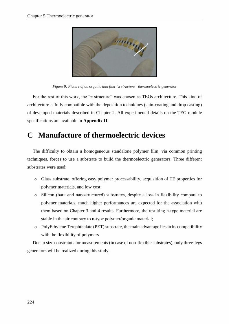
Chapter 5 Thermoelectric generator
224
Figure 9: Picture of an organic thin film “π structure” thermoelectric generator
For the rest of this work, the “π structure” was chosen as TEGs architecture. This kind of
architecture is fully compatible with the deposition techniques (spin-coating and drop casting)
of developed materials described in Chapter 2. All experimental details on the TEG module
specifications are available in Appendix II.
C Manufacture of thermoelectric devices
The difficulty to obtain a homogeneous standalone polymer film, via common printing
techniques, forces to use a substrate to build the thermoelectric generators. Three different
substrates were used:
o Glass substrate, offering easy polymer processability, acquisition of TE properties for
polymer materials, and low cost;
o Silicon (bare and nanostructured) substrates, despite a loss in flexibility compare to
polymer materials, much higher performances are expected for the association with
them based on Chapter 3 and 4 results. Furthermore, the resulting n-type material are
stable in the air contrary to n-type polymer/organic material;
o PolyEthylene Terephthalate (PET) substrate, the main advantage lies in its compatibility
with the flexibility of polymers.
Due to size constraints for measurements (in case of non-flexible substrates), only three-legs
generators will be realized during this study.

Chapter 5 Thermoelectric generator
225
TEG based on glass substrate
As described previously, the most conventional TEG architecture consists of two, p- & n-
type semiconductors materials, connected thermally in parallel and electrically in series.
Nevertheless, this architecture requires two materials with similar thermoelectric properties,
i.e. power factor. The material with lower power factor can potentially affect the overall
performances of the module. In this work, the best p- & n-type polymers have very different
power factors, PF (PEDOT) = 240 µW/mK² and PF (PCBM) = 2.44 µW/mK², as shown studies
in Chapter 2.
A solution developed by several scientist groups was to make TEG modules with only one
material [36–39]. In order to have a functional device, a different architecture has to be realized.
The top electrode of each individual thermoelectric leg had to be connected to the bottom
electrode of the next individual leg, i.e. all legs are connected in a series configuration, as
presented in Figure 10. This architecture is called unileg thermoelectric generator, and this was
applied for all p- & n-type materials available.
As described previously, only the Power Output of the different TEGs modules at different
temperature differences were studied (Figure 11a and 11b). Maximal Power Output was
obtained by the following formula Pout = Voc x Isc, these parameters were measured in a closed
circuit, and for more visibility only Pout versus the temperature difference are presented in
Figure 11.
Figure 10: Picture of an unileg thermoelectric generator with only p-type legs made of PEDOT:Tos on glass
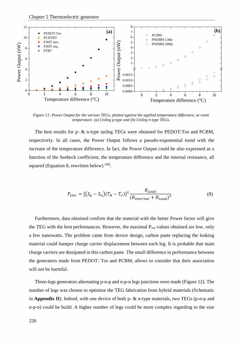
Chapter 5 Thermoelectric generator
226
The best results for p- & n-type unileg TEGs were obtained for PEDOT:Tos and PCBM,
respectively. In all cases, the Power Output follows a pseudo-exponential trend with the
increase of the temperature difference. In fact, the Power Output could be also expressed as a
function of the Seebeck coefficient, the temperature difference and the internal resistance, all
squared (Equation 8, rewritten below) [40].
𝑃𝑒𝑙𝑒𝑐 = [(𝑆𝑝 − 𝑆𝑛)(𝑇𝐻 − 𝑇𝐶)]²𝑅𝐿𝑜𝑎𝑑
(𝑅𝐼𝑛𝑡𝑒𝑟𝑛𝑎𝑙 + 𝑅𝐿𝑜𝑎𝑑)² (8)
Furthermore, data obtained confirm that the material with the better Power factor will give
the TEG with the best performances. However, the maximal Pout values obtained are low, only
a few nanowatts. The problem came from device design, carbon paste replacing the leaking
material could hamper charge carrier displacement between each leg. It is probable that main
charge carriers are dissipated in this carbon paste. The small difference in performance between
the generators made from PEDOT: Tos and PCBM, allows to consider that their association
will not be harmful.
Three-legs generators alternating p-n-p and n-p-n legs junctions were made (Figure 12). The
number of legs was chosen to optimize the TEG fabrication from hybrid materials (Schematic
in Appendix II). Indeed, with one device of both p- & n-type materials, two TEGs (p-n-p and
n-p-n) could be build. A higher number of legs could be more complex regarding to the size
0 2 4 6 8 100
2
4
6
8
10
12
PEDOT:Tos
PCDTBT
P3HT mix.
P3HT seq.
PTB7
Po
wer
Ou
tpu
t (n
W)
Temperature difference (°C)0 2 4 6 8 10
0.0000
0.0005
0.0010
0.0015
1
2
3
4
5
6
7
8
PCBM
PNDIBS LMn
PNDIBS HMn
Po
wer
Ou
tpu
t (n
W)
Temperature difference (°C)
Figure 11: Power Output for the various TEGs, plotted against the applied temperature difference, at room
temperature. (a) Unileg p-type and (b) Unileg n-type TEGs.
(a) (b)

Chapter 5 Thermoelectric generator
227
restriction with our measurement equipment (Appendix II). Furthermore, based on Equation 8,
the increase of the number of legs will result in an increase of the first term (Sp-Sn).(TH-TC)²
but also of the global electrical resistance. So depending of the resistance value for one leg,
increasing the number of legs could have a negative impact on the Power generated. Finally,
based on Chapter 2 and previous results, only PCBM were used as n-type material.
Unfortunately, as predicted, a mixture of p- & n-type legs had a negative effect on the
maximal Pout measured (Figure 13). By comparing results obtained for p-n-p and n-p-n junction,
p-type polymer does not affect the performance. PCBM is the material which has a negative
impact on performances, as proven by the fact that n-p-n junction is worse than p-n-p one. The
difference in thermoelectric properties is detrimental for the construction of efficient TEG,
materials must have the same thermoelectric properties. It is noteworthy that all TEGs with
PCBM were tested under controlled atmosphere, inside a glovebox. When the measurements
were conducted outside the glovebox, with air and moisture, no performances were obtained.
Indeed, it is recognized that PCBM is sensible to oxygen. Studies have been performed on the
photo-oxidation of C60 molecules by Xia et al. where they have reported that interaction
between oxygen and C60 molecules, induced by irradiation, may occur and can be described as
C60 → C60On + O2, (n = 1–5) [41]. The properties of fullerene to trap the radicals by the reaction
of radical addition lead to the formation of radical sites which can initiate its own degradation
and disturb the charge carriers’ displacement.
Figure 12: Picture of p-n-p three-legs thermoelectric generator with p-type legs made of PEDOT:Tos and n-
type leg made with PCBM on glass

Chapter 5 Thermoelectric generator
228
TEG based on silicon substrate
In the previous part, low performances and poor stability were obtained for polymer/organic
TEGs. Furthermore, this study showed the importance of having two materials with the same
thermoelectric properties. The strategy developed in our laboratory was the use of silicon as a
substrate to overcome these drawbacks. Silicon substrates were chosen as semi-conducting
inorganic material due to their important role in electronic and industrial field [42], their high
range of impurities concentration (doping concentration) accessible [43], their good
thermoelectric properties (S ≈ 500-1200 µV/K when correctly doped) at room temperature [44]
and their air stability even for n-type silicon. Different polymers combined with silicon
substrates with various electrical conductivities and Seebeck coefficients [45] , described in
Chapter 3 and 4, were used as material for TEG construction. The corresponding hybrid
materials should benefit from the advantages of the two components, hindering their
corresponding drawbacks.
The compatibility between thermoelectric properties being essential, thermoelectric
generators were made with an alternation of p- & n-type silicon substrates with the same
electrical conductivity. In Chapter 3, the study of the influence of polymer thickness on the
thermoelectric properties has showed that the same absolute value, Seebeck coefficient and
electrical conductivity, were obtained whatever the silicon doping nature. So, thermoelectric
generators based on these results were made, and their performances were evaluated. Thanks
to the air stability of silicon, most of the devices were tested outside a glovebox, yet PCBM
samples have been measured inside the glovebox.
0 2 4 6 8 10
0
2
4
6
8
10
PEDOT:Tos
PCBM
PEDOT-PCBM-PEDOT
PCBM-PEDOT-PCBM
PCDTBT-PCBM-PCDTBT
PCBM-PCDTBT-PCBM
P3HT-PCBM-P3HT
PCBM-P3HT-PCBMP
ow
er O
utp
ut
(nW
)
Temperature difference (°C)
Figure 1310: Power Output for the various TEGs, plotted against the applied temperature difference, at room
temperature.
Black symbols correspond to unileg PEDOT:Tos (full) and PCBM (empty). Then, full and empty colored
symbols represent p-n-p and n-p-n three-legs TEGs on glass, respectively.
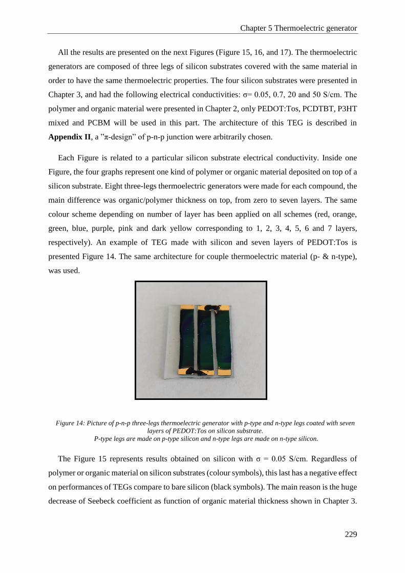
Chapter 5 Thermoelectric generator
229
All the results are presented on the next Figures (Figure 15, 16, and 17). The thermoelectric
generators are composed of three legs of silicon substrates covered with the same material in
order to have the same thermoelectric properties. The four silicon substrates were presented in
Chapter 3, and had the following electrical conductivities: σ= 0.05, 0.7, 20 and 50 S/cm. The
polymer and organic material were presented in Chapter 2, only PEDOT:Tos, PCDTBT, P3HT
mixed and PCBM will be used in this part. The architecture of this TEG is described in
Appendix II, a ”π-design” of p-n-p junction were arbitrarily chosen.
Each Figure is related to a particular silicon substrate electrical conductivity. Inside one
Figure, the four graphs represent one kind of polymer or organic material deposited on top of a
silicon substrate. Eight three-legs thermoelectric generators were made for each compound, the
main difference was organic/polymer thickness on top, from zero to seven layers. The same
colour scheme depending on number of layer has been applied on all schemes (red, orange,
green, blue, purple, pink and dark yellow corresponding to 1, 2, 3, 4, 5, 6 and 7 layers,
respectively). An example of TEG made with silicon and seven layers of PEDOT:Tos is
presented Figure 14. The same architecture for couple thermoelectric material (p- & n-type),
was used.
The Figure 15 represents results obtained on silicon with σ = 0.05 S/cm. Regardless of
polymer or organic material on silicon substrates (colour symbols), this last has a negative effect
on performances of TEGs compare to bare silicon (black symbols). The main reason is the huge
decrease of Seebeck coefficient as function of organic material thickness shown in Chapter 3.
Figure 14: Picture of p-n-p three-legs thermoelectric generator with p-type and n-type legs coated with seven
layers of PEDOT:Tos on silicon substrate.
P-type legs are made on p-type silicon and n-type legs are made on n-type silicon.

Chapter 5 Thermoelectric generator
230
However, a slight difference between all the Power Output obtained for TEG could be explained
by the difference of electrical conductivity of the organic material.
Thereafter, silicon with an electrical conductivity of σ = 0.7 S/cm was used as substrate in
the study of the influence of organic material thickness on TEG performances (Figure 16).
Organic materials have still a negative impact on performances of TEG hybrid devices. The
most remarkable case is the TEG with PCBM, despite the low electrical conductivity of the
latter, the negative effect is not very important (compare to the PCDTBT or P3HT with barely
the same electrical conductivity). This is important to note that this effect is less important
compared to TEG made with lower conductive silicon. In the first approximation, this is
possible to say that the thermoelectric properties of the substrate are very important for the
hybrid assembly. Indeed, the substrate accounts for more than 90% of the thickness of the
device.
0 2 4 6 8 100
1
2
3
4
Bare Silicon
1 layer PEDOT
2 layer PEDOT
3 layer PEDOT
4 layer PEDOT
5 layer PEDOT
6 layer PEDOT
7 layer PEDOT
Po
wer
Ou
tpu
t (n
W)
Temperature difference (°C)
0 2 4 6 8 100
1
2
3
4
Bare Silicon
1 layer P3HT
2 layer P3HT
3 layer P3HT
4 layer P3HT
5 layer P3HT
6 layer P3HT
7 layer P3HT
Po
wer
Ou
tpu
t (n
W)
Temperature difference (°C)
0 2 4 6 8 100
1
2
3
4
Bare Silicon
1 layer PCDTBT
2 layer PCDTBT
3 layer PCDTBT
4 layer PCDTBT
5 layer PCDTBT
6 layer PCDTBT
7 layer PCDTBT
Pow
er O
utp
ut
(nW
)
Temperature difference (°C)0 2 4 6 8 10
0
1
2
3
4
Bare Silicon
1 layer PCBM
2 layer PCBM
3 layer PCBM
4 layer PCBM
5 layer PCBM
6 layer PCBM
7 layer PCBM
Pow
er O
utp
ut
(nW
)
Temperature difference (°C)
(a) (b)
(c) (d)
Figure 15: Power Output for the various TEGs, plotted against the applied temperature difference, at room
temperature.
p-n-p three-legs TEGs on silicon substrate (σ=0.05 S/cm) with (a) PEDOT:Tos, (b) P3HT, (c) PCDTBT and
(d) PCBM with different thickness coated on top.

Chapter 5 Thermoelectric generator
231
Finally, Figure 17 gathers the results for hybrid TEGs based on silicon with electrical
conductivity of σ = 20 and 50 S/cm. In all cases, PCDTBT has a negative effect on Power
Output. Then, following the electrical conductivity of the silicon substrate, P3HT and PCBM
obtained different results. For the silicon substrate at σ = 20 S/cm, the same behaviour as low
conductive silicon (σ =0.05 and 0.7 S/cm), were obtained for P3HT, the stacking of polymer
layers on top of the substrate decreases the TEG performance. The PCBM thickness does not
have any impact on TEG performances for silicon with σ = 20 S/cm. For the silicon substrate
at σ = 50 S/cm, opposing behaviours are worth noting. In fact, the P3HT has a positive effect
on the performance of the hybrid TEG, whereas in the case of the PCBM a decrease occurs.
This decrease in performance is surprising, based on the previous results, an increase may
occur. This effect could be attributed to an experimental problem related to the thermoelectric
generator itself (contact problems for example). The best effects were obtained for PEDOT:Tos
on both silicon (σ = 20 and 50 S/cm). When the Seebeck coefficient stays constant while the
electrical conductivity increases, a better power factor is obtained, and so the Power Output
resulting is better. Record value of 1795 nW at ΔT = 10K was obtained for five layers of
PEDOT:Tos on silicon with an electrical conductivity of 50 S/cm.
0 2 4 6 8 100
5
10
15
20
25
30
Bare Silicon
1 layer P3HT
2 layer P3HT
3 layer P3HT
4 layer P3HT
5 layer P3HT
6 layer P3HT
7 layer P3HT
Pow
er O
utp
ut
(nW
)
Temperature difference (°C)
0 2 4 6 8 100
5
10
15
20
25
30
Bare Silicon
1 layer PCDTBT
2 layer PCDTBT
3 layer PCDTBT
4 layer PCDTBT
5 layer PCDTBT
6 layer PCDTBT
7 layer PCDTBT
Po
wer
Ou
tpu
t (n
W)
Temperature difference (°C)
0 2 4 6 8 100
5
10
15
20
25
30
Bare Silicon
1 layer PCBM
2 layer PCBM
3 layer PCBM
4 layer PCBM
5 layer PCBM
6 layer PCBM
7 layer PCBM
Po
wer
Ou
tpu
t (n
W)
Temperature difference (°C)
0 2 4 6 8 100
5
10
15
20
25
30
Bare Silicon
1 layer PEDOT
2 layer PEDOT
3 layer PEDOT
4 layer PEDOT
5 layer PEDOT
6 layer PEDOT
7 layer PEDOT
Po
wer
Ou
tpu
t (n
W)
Temperature difference (°C)
(a) (b)
(c) (d)
Figure 16: Power Output for the various TEGs, plotted against the applied temperature difference, at room
temperature. p-n-p three-legs TEGs on silicon substrate (σ=0.7 S/cm) with (a) PEDOT:Tos, (b) P3HT, (c)
PCDTBT and (d) PCBM with different thickness coated on top.

Chapter 5 Thermoelectric generator
232
0 2 4 6 8 100
100
200
300
400
500
600
700
Bare Silicon
1 layer PEDOT
2 layer PEDOT
3 layer PEDOT
4 layer PEDOT
5 layer PEDOT
6 layer PEDOT
7 layer PEDOT
Pow
er O
utp
ut
(nW
)
Temperature difference (°C)
0 2 4 6 8 100
500
1000
1500
2000
Bare Silicon
1 layer PEDOT
2 layer PEDOT
3 layer PEDOT
4 layer PEDOT
5 layer PEDOT
6 layer PEDOT
7 layer PEDOT
Po
wer
Ou
tpu
t (n
W)
Temperature difference (°C)
0 2 4 6 8 100
100
200
300
400
500
600
Bare Silicon
1 layer P3HT
2 layer P3HT
3 layer P3HT
4 layer P3HT
5 layer P3HT
6 layer P3HT
7 layer P3HT
Pow
er O
utp
ut
(nW
)
Temperature difference (°C)
0 2 4 6 8 100
200
400
600
800
1000
Bare Silicon
1 layer P3HT
2 layer P3HT
3 layer P3HT
4 layer P3HT
5 layer P3HT
6 layer P3HT
7 layer P3HT
Po
wer
Ou
tpu
t (n
W)
Temperature difference (°C)
0 2 4 6 8 100
200
400
600
800
Bare Silicon
1 layer PCDTBT
2 layer PCDTBT
3 layer PCDTBT
4 layer PCDTBT
5 layer PCDTBT
6 layer PCDTBT
7 layer PCDTBT
Po
wer
Ou
tpu
t (n
W)
Temperature difference (°C)
0 2 4 6 8 100
100
200
300
400
500
600
Bare Silicon
1 layer PCDTBT
2 layer PCDTBT
3 layer PCDTBT
4 layer PCDTBT
5 layer PCDTBT
6 layer PCDTBT
7 layer PCDTBT
Pow
er O
utp
ut
(nW
)
Temperature difference (°C)0 2 4 6 8 10
0
100
200
300
400
500
600
Bare Silicon
1 layer PCBM
2 layer PCBM
3 layer PCBM
4 layer PCBM
5 layer PCBM
6 layer PCBM
7 layer PCBM
Po
wer
Ou
tpu
t (n
W)
Temperature difference (°C)
0 2 4 6 8 100
200
400
600
800
Bare Silicon
1 layer PCBM
2 layer PCBM
3 layer PCBM
4 layer PCBM
5 layer PCBM
6 layer PCBM
7 layer PCBM
Pow
er O
utp
ut
(nW
)
Temperature difference (°C)
Figure 17: Power Output for the various TEGs, plotted against the applied temperature difference, at room
temperature.
p-n-p three-legs TEGs on silicon substrate (σ=20 S/cm) with (a) PEDOT:Tos, (b) P3HT, (c) PCDTBT and (d)
PCBM with different thickness coated on top.
p-n-p three-legs TEGs on silicon substrate (σ=50 S/cm) with (e) PEDOT:Tos, (f) P3HT, (g) PCDTBT and (h)
PCBM with different thickness coated on top.
(a) (b)
(c) (d)
(e) (f)
(g) (h)

Chapter 5 Thermoelectric generator
233
Like in the case of TEG on glass, a silicon TEG was made with two organic materials,
p- & n-type (Figure 18). The best organic materials were used, PEDOT:Tos as a p-type and
PCBM as a n-type material. So each of these compounds were deposited on silicon with the
same majority charge carriers. The same three-legs “π-architecture” with p-n-p junctions was
done. The results are all presented in Figure 18. Figure 18a compares efficiency of full
PEDOT:Tos device (empty dots) and PEDOT:Tos / PCBM devices (full dots), while Figure
18b compares efficiency of full PCBM (empty squares) and PEDOT:Tos / PCBM devices (full
dots). If the thermoelectric properties of the two organic materials had been similar, an increase
in Power Output would have to happen. As this is not the case, the PCBM has a "negative"
impact on the overall performance of the device. This effect is even more true that the PEDOT
has a positive effect, when compared with the device made entirely with PCBM. These results,
highlighted by the previous results (Figure 13), have also again shown the importance of having
very similar thermoelectric characteristics.
Of all the organic materials synthesized or provided in Chapter 3, the p-type materials
showed the best results. PEDOT:Tos which after a fine optimization showed a high power
factor resulting from his good thermoelectric. Subsequently, the results of thermoelectric
generators based on silicon, showed the importance of substrate intrinsic properties.
So silicon with high surface area, developed in Chapter 4, were used as substrates to obtain
more efficient hybrid TEGs. Only PEDOT:Tos which obtain the best thermoelectric
performances will be deposited on nanostructured silicon. Figure 19 presents the efficiency of
TEGs built with this nanostructured silicon and different PEDOT:Tos thicknesses. As a
0 2 4 6 8 100
500
1000
1500
2000
Bare Silicon
1 layer PEDOT-PCBM-PEDOT
2 layer PEDOT-PCBM-PEDOT
3 layer PEDOT-PCBM-PEDOT
4 layer PEDOT-PCBM-PEDOT
5 layer PEDOT-PCBM-PEDOT
6 layer PEDOT-PCBM-PEDOT
7 layer PEDOT-PCBM-PEDOT
1 layer PEDOT
2 layer PEDOT
3 layer PEDOT
4 layer PEDOT
5 layer PEDOT
6 layer PEDOT
7 layer PEDOT
Pow
er O
utp
ut
(nW
)
Temperature difference (°C)
0 2 4 6 8 100
500
1000
1500
2000
Bare Silicon
1 layer PEDOT-PCBM-PEDOT
2 layer PEDOT-PCBM-PEDOT
3 layer PEDOT-PCBM-PEDOT
4 layer PEDOT-PCBM-PEDOT
5 layer PEDOT-PCBM-PEDOT
6 layer PEDOT-PCBM-PEDOT
7 layer PEDOT-PCBM-PEDOT
1 layer PCBM
2 layer PCBM
3 layer PCBM
4 layer PCBM
5 layer PCBM
6 layer PCBM
7 layer PCBM
Pow
er O
utp
ut
(nW
)
Temperature difference (°C)
(a) (b)
Figure 18: Power Output for the various TEGs, plotted against the applied temperature difference, at room
temperature.
Comparison of p-n-p three-legs TEGs on silicon substrate (σ=50 S/cm)[full symbols] versus
(a) unileg PEDOT:Tos and (b) unileg PCBM TEGs [empty symbols].

Chapter 5 Thermoelectric generator
234
reference, Figure 19a is the result obtained for bare silicon with PEDOT:Tos. As described in
Chapter 4, the increase in the area between the polymer and the substrate induces an increase
in thermoelectric properties. Thus, the best results were obtained for TEGs based on SiNWs
coated with 6 layers of PEDOT: Tos, Pout = 2350 nW. By modifying the silicon structure at a
nanometric scale, a 25 % increase of the Power Output was realized. It is noteworthy that as
expected the increase of temperature difference has a direct impact on the Power Output. The
first term of the Equation 8, (Sp-Sn).(TH-TC)², explains this phenomenon, the temperature has
the same impact than the Seebeck coefficient difference.
0 2 4 6 8 100
500
1000
1500
2000
2500
Si NWs
1 layer PEDOT on Si NWs
2 layer PEDOT on Si NWs
3 layer PEDOT on Si NWs
4 layer PEDOT on Si NWs
5 layer PEDOT on Si NWs
6 layer PEDOT on Si NWs
7 layer PEDOT on Si NWs
Po
wer
Ou
tpu
t (n
W)
Temperature difference (°C)
0 2 4 6 8 100
500
1000
1500
2000
2500
Bare Silicon
1 layer PEDOT
2 layer PEDOT
3 layer PEDOT
4 layer PEDOT
5 layer PEDOT
6 layer PEDOT
7 layer PEDOT
Pow
er O
utp
ut
(nW
)
Temperature difference (°C)0 2 4 6 8 10
0
500
1000
1500
2000
2500
Si Pyramids
1 layer PEDOT on Si Pyramids
2 layer PEDOT on Si Pyramids
3 layer PEDOT on Si Pyramids
4 layer PEDOT on Si Pyramids
5 layer PEDOT on Si Pyramids
6 layer PEDOT on Si Pyramids
7 layer PEDOT on Si Pyramids
Pow
er O
utp
ut
(nW
)
Temperature difference (°C)
0 2 4 6 8 10
0
500
1000
1500
2000
2500
Si Porous
1 layer PEDOT on Si Porous
2 layer PEDOT on Si Porous
3 layer PEDOT on Si Porous
4 layer PEDOT on Si Porous
5 layer PEDOT on Si Porous
6 layer PEDOT on Si Porous
7 layer PEDOT on Si Porous
Pow
er O
utp
ut
(nW
)
Temperature difference (°C)
(a) (b)
(c) (d)
Figure 19: Power Output for the various TEGs, plotted against the applied temperature difference, at room
temperature.
Comparison of p-n-p three-legs TEGs on silicon substrate (σ=50 S/cm), (a) bare silicon, (b) silicon pyramids,
(c) porous silicon and (d) silicon nanowires with different PEDOT:Tos thickness coated on top.
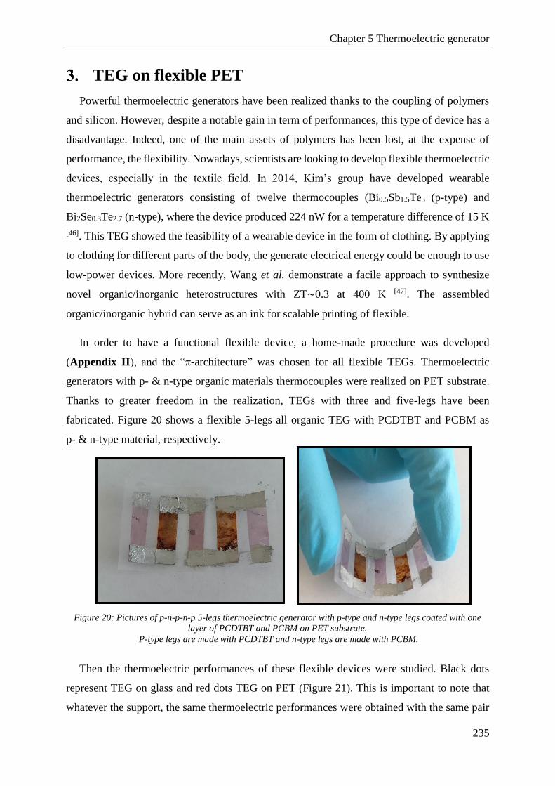
Chapter 5 Thermoelectric generator
235
TEG on flexible PET
Powerful thermoelectric generators have been realized thanks to the coupling of polymers
and silicon. However, despite a notable gain in term of performances, this type of device has a
disadvantage. Indeed, one of the main assets of polymers has been lost, at the expense of
performance, the flexibility. Nowadays, scientists are looking to develop flexible thermoelectric
devices, especially in the textile field. In 2014, Kim’s group have developed wearable
thermoelectric generators consisting of twelve thermocouples (Bi0.5Sb1.5Te3 (p-type) and
Bi2Se0.3Te2.7 (n-type), where the device produced 224 nW for a temperature difference of 15 K
[46]. This TEG showed the feasibility of a wearable device in the form of clothing. By applying
to clothing for different parts of the body, the generate electrical energy could be enough to use
low-power devices. More recently, Wang et al. demonstrate a facile approach to synthesize
novel organic/inorganic heterostructures with ZT∼0.3 at 400 K [47]. The assembled
organic/inorganic hybrid can serve as an ink for scalable printing of flexible.
In order to have a functional flexible device, a home-made procedure was developed
(Appendix II), and the “π-architecture” was chosen for all flexible TEGs. Thermoelectric
generators with p- & n-type organic materials thermocouples were realized on PET substrate.
Thanks to greater freedom in the realization, TEGs with three and five-legs have been
fabricated. Figure 20 shows a flexible 5-legs all organic TEG with PCDTBT and PCBM as
p- & n-type material, respectively.
Then the thermoelectric performances of these flexible devices were studied. Black dots
represent TEG on glass and red dots TEG on PET (Figure 21). This is important to note that
whatever the support, the same thermoelectric performances were obtained with the same pair
Figure 20: Pictures of p-n-p-n-p 5-legs thermoelectric generator with p-type and n-type legs coated with one
layer of PCDTBT and PCBM on PET substrate.
P-type legs are made with PCDTBT and n-type legs are made with PCBM.

Chapter 5 Thermoelectric generator
236
of materials. Some measurements were done under a small bending between fingers as proof
of concept. TEGs were still working without any loss in performances until the electrodes break.
In fact, electrodes were deposited manually and they were very fragile. Design improvements
are to be expected such as silver electrode deposited by thermal evaporation.
In addition, the increase of the number of legs allows an increase in Power Output (Figure 21,
blue dots). However, as explain previously, increasing the number of legs will not necessarily
increase the resulting Power Output. By increasing the number of legs, the internal resistance
of the device also increases. It is, therefore, logical to think that despite the increase in the
voltage generated (addition of legs, so the addition of Seebeck coefficient), the resistance of the
device is an issue. This reason explains why few generators with a large number of legs (more
than 1000 legs) are developed (internal electrical and contact resistance are very high) [48–51].
0 2 4 6 8 100.0
0.5
1.0
1.5
2.0
2.5
3.0
PEDOT-PCBM-PEDOT (glass)
PEDOT-PCBM-PEDOT (PET)
5-legs PEDOT-PCBM (PET)
Pow
er O
utp
ut
(nW
)
Temperature difference (°C)
0 2 4 6 8 100.0
0.5
1.0
1.5
2.0
2.5
3.0
P3HT-PCBM-P3HT (glass)
P3HT-PCBM-P3HT (PET)
5-legs P3HT-PCBM (PET)
Po
wer
Ou
tpu
t (n
W)
Temperature difference (°C)
0 2 4 6 8 100.0
0.5
1.0
1.5
2.0
2.5
3.0
PCDTBT-PCBM-PCDTBT (glass)
PCDTBT-PCBM-PCDTBT (PET)
5-legs PCDTBT-PCBM (PET)
Po
wer
Ou
tpu
t (n
W)
Temperature difference (°C)
(a) (b)
(c)
Figure 21: Power Output for the various TEGs, plotted against the applied temperature difference, at room
temperature.
Comparison of p-n-p three-legs TEGs on glass vs PET substrates with (a) PEDOT:Tos, (b) P3HT and (c)
PCDTBT.
Chapter 5 Thermoelectric generator
237
D Conclusion
In this present study, thermoelectric generators on various support were developed for near
room temperature application. Full organic TEGs, on glass and PET, showed similar
performances. Despite their low Power Output, this kind of devices are proof of concept to
develop more efficient material. The main issue was the low stability (absence of electrical
conductivity) of the n-type material resulting in low performances.
In parallel, TEGs on silicon substrates were fabricated. In case of high conductive silicon,
the coupling with organic material achieved to obtain an enhancement of device performances.
Furthermore, the interface between the organic material and the substrate had a crucial role in
this phenomenon. By nanostructuring silicon surface, better performances were obtain for
hybrid PEDOT:Tos-silicon thermoelectric generators. An increase was achieved thanks to this
fine tuning of interface between silicon and organic material. To explain this enhancement, a
charge transfer at the silicon-organic interface was suspected [17], thus resulting to a record high
power of 2350 nW, for three-legs generator at ΔT = 10K near room temperature.
Unfortunately, this enhancement could not be verified even with high analytical techniques.
These results are in agreement with recent studies on hybrid systems. Scientists have focused
on the use of various strategies (interfacial transport and structural/morphological effects) to
improve the thermoelectric performance. However, it was proven difficult to establish the
fundamental physics driving these performance enhancements [52,53]. The development of the
next generation hybrid thermoelectric materials and device requires an improvement in the
understanding of the carrier transport physics in complex multiphase systems.
Finally, it would be wise to homogenize the reporting of results related to TEGs. Indeed, it
is difficult to compare the performance of TEGs at present. Each team uses its own architecture,
the size and number of legs are rarely similar. It is especially in the conditions of analysis, that
the greatest differences occur. Performances can be drastically changed if the temperature
gradient is achieved at room temperature or under heating. Data that is rarely provided by the
authors [16,54,55].

Chapter 5 Thermoelectric generator
238
References
[1] J. He, T. M. Tritt, Science 2017, 357, eaak9997.
[2] L.-D. Zhao, G. Tan, S. Hao, J. He, Y. Pei, H. Chi, H. Wang, S. Gong, H. Xu, V. P.
Dravid, C. Uher, G. J. Snyder, C. Wolverton, M. G. Kanatzidis, Science 2016, 351,
141.
[3] V. J Lyons, G. A. Gonzalez, M. G. Houts, C. J. Iannello, J. H. Scott, S. Surampudi,
DRAFT Space Power and Energy Storage Roadmap - Technologye area 03, NASA,
2010.
[4] R. L. Cataldo, G. L. Bennett, Radioisot. - Appl. Phys. Sci. 2011.
[5] M. Brignone, A. Ziggiotti, AIP Conf. Proc. 2012, 1449, 493.
[6] B. Mazar (March 21 2012), State of the art prototype vehicle with a thermoelectric
generator, BMW Group, view on:
https://www1.eere.energy.gov/vehiclesandfuels/pdfs/thermoelectrics_app_2012/wed
nesday/mazar.pdf (July, 2019).
[7] M. Brunetti, A. Cogliati, D. Iannucci, A. Scandroglio, Aircraft capable of hovering
having an exhaust duct with thermoelectric conversion circuit, 2015.
[8] N. R. Kristiansen, G. J. Snyder, H. K. Nielsen, L. Rosendahl, J. Electron. Mater. 2012,
41, 1024.
[9] BioLite Inc., CampStove 2 view on: https://eu.bioliteenergy.com/products/campstove-
2 (July, 2019).
[10] D. Champier, J. P. Bedecarrats, M. Rivaletto, F. Strub, Energy 2010, 35, 935.
[11] G. F. Rinalde, L. E. Juanicó, E. Taglialavore, S. Gortari, M. G. Molina, Int. J. Hydrog.
Energy 2010, 35, 5818.
[12] M. F. Silva, J. F. Ribeiro, J. P. Carmo, L. M. Gonçalves, J. H. Correia, In Scanning
Probe Microscopy in Nanoscience and Nanotechnology 3; Bhushan, B., Ed.;
NanoScience and Technology; Springer Berlin Heidelberg: Berlin, Heidelberg, 2013;
pp. 485–528.
[13] M. Orrill, S. LeBlanc, J. Appl. Polym. Sci. 2017, 134.
[14] Gordon B. Haxel, James B. Hedrick, and Greta J. Orris, USGS 2002, Fact Sheet 087-
02.
[15] N. Lowhorn, W. K. Wong-Ng, J. Lu, E. L. Thomas, M. Otani, M. L. Green, N. Dilley,
J. Sharp, T. N. Tran, Appl. Phys. -Mater. Sci. Process. 2009, 96.
[16] B. Russ, A. Glaudell, J. J. Urban, M. L. Chabinyc, R. A. Segalman, Nat. Rev. Mater.
2016, 1, 16050.
[17] Y. Zhang, S.-J. Park, Polymers 2019, 11.
[18] S. M. Haque, J. A. A. Rey, A. AbubakarMasúd, Y. Umar, R. Albarracin, Prop. Appl.
Polym. Dielectr. 2017.
[19] B. Russ, A. Glaudell, J. J. Urban, M. L. Chabinyc, R. A. Segalman, Nat. Rev. Mater.
2016, 1, 16050.
[20] Hideyoshi Kume (Feb6, 2013), Fujifilm Shows High-efficiency Thermoelectric
Converter Using Organic Material, view on:
https://tech.nikkeibp.co.jp/dm/english/NEWS_EN/20130206/264517/ (July, 2019)
[21] R. Tian, C. Wan, N. Hayashi, T. Aoai, K. Koumoto, MRS Bull. 2018, 43, 193.
[22] R. Kroon, D. A. Mengistie, D. Kiefer, J. Hynynen, J. D. Ryan, L. Yu, C. Müller, Chem.
Soc. Rev. 2016, 45, 6147.
[23] C. E. Kinsella, S. M. O’Shaughnessy, M. J. Deasy, M. Duffy, A. J. Robinson, 2014.
[24] D. M. Rowe, G. Min, J. Power Sources 1998, 73, 193.

Chapter 5 Thermoelectric generator
239
[25] C. Goupil, W. Seifert, K. Zabrocki, E. Müller, G. J. Snyder, Entropy 2011, 13, 1481.
[26] O. Bubnova, X. Crispin, Energy Environ. Sci. 2012, 5, 9345.
[27] K. Uchida, M. Ishida, T. Kikkawa, A. Kirihara, T. Murakami, E. Saitoh, J. Phys.
Condens. Matter 2014, 26, 343202.
[28] Y. Kishita, Y. Ohishi, M. Uwasu, M. Kuroda, H. Takeda, K. Hara, J. Clean. Prod.
2016, 126, 607.
[29] P. M. Kumar, V. Jagadeesh Babu, A. Subramanian, A. Bandla, N. Thakor, S.
Ramakrishna, H. Wei, Designs 2019, 3, 22.
[30] O. Bubnova, Z. U. Khan, A. Malti, S. Braun, M. Fahlman, M. Berggren, X. Crispin,
Nat. Mater. 2011, 10, 429.
[31] V. Jovovic, Thermoelectric Waste Heat Recovery Program for Passenger Vehicles;
Gentherm Incorporated, Azusa, CA (United States), 2015.
[32] A. K. Menon, S. K. Yee, J. Appl. Phys. 2016, 119, 055501.
[33] A. K. Menon, O. Meek, A. J. Eng, S. K. Yee, J. Appl. Polym. Sci. 2017, 134.
[34] F. Suarez, A. Nozariasbmarz, D. Vashaee, M. C. Öztürk, Energy Environ. Sci. 2016,
9, 2099.
[35] F. Jiao, C. Di, Y. Sun, P. Sheng, W. Xu, D. Zhu, Philos. Transact. A Math. Phys. Eng.
Sci. 2014, 372, 20130008.
[36] I. Dani, A. Roch, L. Stepien, C. Leyens, M. Greifzu, M. von Lukowicz, In Digital
Product and Process Development Systems; Kovács, G. L.; Kochan, D., Eds.; IFIP
Advances in Information and Communication Technology; Springer Berlin
Heidelberg, 2013; pp. 181–184.
[37] K. Suemori, S. Hoshino, T. Kamata, Appl. Phys. Lett. 2013, 103, 153902.
[38] S. Hwang, W. J. Potscavage, R. Nakamichi, C. Adachi, Org. Electron. 2016, 31, 31.
[39] W. Wijesekara, L. Rosendahl, D. R. Brown, G. J. Snyder, J. Electron. Mater. 2015,
44, 1834.
[40] F. Cheng, Thermoelectr. Power Gener. - Look Trends Technol. 2016.
[41] A. D. Xia, S. Wada, H. Tashiro, Appl. Phys. Lett. 1998, 73, 1323.
[42] L. Venema, Nature 2011, 479, 309.
[43] Bar J. Van Zeghbroeck (1996-1997), 2.9 Mobility - Resistivity - Sheet Resistance,
Colorado University, view on: http://ecee.colorado.edu/~bart/book/mobility.htm
(July, 2019).
[44] J. Zhou, B. Liao, B. Qiu, S. Huberman, K. Esfarjani, M. S. Dresselhaus, G. Chen, Proc.
Natl. Acad. Sci. 2015, 112, 14777.
[45] A. W. Van Herwaarden, Sens. Actuators 1984, 6, 245.
[46] M.-K. Kim, M.-S. Kim, S. Lee, C. Kim, Y.-J. Kim, Smart Mater. Struct. 2014, 23,
105002.
[47] L. Wang, Z. Zhang, L. Geng, T. Yuan, Y. Liu, J. Guo, L. Fang, J. Qiu, S. Wang, Energy
Environ. Sci. 2018, 11, 1307.
[48] Y. Wang, S. M. Zhang, Y. Deng, J. Mater. Chem. A 2016, 4, 3554.
[49] L. Wang, Q. Yao, W. Shi, S. Qu, L. Chen, Mater. Chem. Front. 2017, 1, 741.
[50] H. Fang, B. C. Popere, E. M. Thomas, C.-K. Mai, W. B. Chang, G. C. Bazan, M. L.
Chabinyc, R. A. Segalman, J. Appl. Polym. Sci. 2017, 134.
[51] A. Fabian-Mijangos, J. Alvarez-Quintana, Bringing Thermoelectricity into Realality
2018 (DOI: 10.5772/intechopen.75790).
[52] N. E. Coates, S. K. Yee, B. McCulloch, K. C. See, A. Majumdar, R. A. Segalman, J.
J. Urban, Adv. Mater. 2013, 25, 1629.
[53] J. Choi, J. Y. Lee, S.-S. Lee, C. R. Park, H. Kim, Adv. Energy Mater. 2016, 6, 1502181.
[54] H. Wang, C. Yu, Joule 2019, 3, 53.
[55] L. C. Ding, A. Akbarzadeh, L. Tan, Renew. Sustain. Energy Rev. 2018, 81, 799.

240

General Conclusion
241
General Conclusion
Organic and hybrid thermoelectricity is a field that is still in its infancy and presents a lot of
exploration opportunities. The recent emergence of connected and communication
technologies, as well as energy issues and the threat of global warming, could make organic
and hybrid thermoelectric devices an important market. For thermoelectric products to find their
place in this context of emerging new technologies, it is still necessary to overcome barriers
related to the performance and manufacturing processes of thermoelectric devices.
The main objective of this Ph.D. thesis, the fabrication of an efficient polymer thermoelectric
material was successfully tackled. The basic philosophy of the work was to optimize the
thermoelectric properties of various organic materials towards efficient thermoelectric design.
Then, the interfacial effects between the silicon substrate and organic materials were utilized to
fabricate a hybrid thermoelectric generator thanks to a novel approach developed.
P-type polymers synthesized were tuned via various different methods, all of which had
played on the doping level analog to the carrier concentration of the material. The n-type
organic materials were characterized, and despite poor air stability, they showed interesting
thermoelectric properties with respect to literature values. Thanks to a fine tuning of electronic
properties, PEDOT:Tos with a power factor of 240 µW/mK² and PCBM with a power factor of
2.44 µW/mK² were the best materials for p- & n-type series. It is noteworthy that a new
n-type polymer PNDIBS with selenium atoms, developed by Prof. Jenekhe’s group, obtained
similar results than standard PNDI(2OD)2T n-type polymer. Unfortunately, no air stable n-type
organic material was recorded.
In Chapter 3, all organic materials were combined with p and n type silicon wafers.
Thermoelectric properties, Seebeck coefficient, electrical conductivity and power factor were
measured for each hybrid material. The results showed an interesting behaviour via increasing
the thickness of the polymer layer, in fact thermoelectric properties could be tuned with this
strategy. Although the origin of this behaviour is not completely clarified, it could be appointed
to interfacial charge transfer phenomena.
The shortage of n-type thermoelectric materials (strongly related to their instability to
ambient air) has forced to propose new synthesis approaches for these materials. The novel
approach, with silicon substrate and organic material on top, enabled the development of an

General Conclusion
242
efficient air stable n-type material for thermoelectric applications. In fact, the impurities inside
the silicon substrate greatly influenced the charge carrier type in the hybrid material. Thus, with
negatively doped silicon, the corresponding devices were of n-type (regarding its Seebeck
coefficient), despite the fact that organic material of p-type had been deposited above them.
The hybrid PEDOT:Tos/n-type silicon reached a record value of 0.65 mW/mK², one of the best
value reported for hybrid n-type material.
Chapter 4, where the silicon surface was nanostructured, provided further insight on the
interface role in properties. In fact, increasing the specific area produces an enhancement of the
thermoelectric properties compared to bare silicon. Despite only employing PEDOT:Tos, this
strategy is suspected to be applied to any organic material, and the same enhancement should
be obtained.
Finally, thermoelectric generators were fabricated by using these hybrid systems and their
behaviour was recorded with respect to the temperature difference. The best power output,
2350 nW, was obtained for three-legs TEG of six PEDOT:Tos layers on silicon nanowires at
temperature difference of 10K. Furthermore, as proof of concept, full organic flexible TEGs
were developed, the same performances under binding were obtained compared to TEGs on
glass.

Perspectives
243
Perspectives
Our study was designed to address different aspects and problems of thermoelectricity in the
organic field. Each of them still requires additional studies. The prospects are numerous, and
listed below:
o As far as materials are concerned, the thermal conductivity of the different organic and
hybrid materials presented in this study should first be determined. In addition, it would
be necessary to increase the thermoelectric performance of p- & n-type materials. In the
case of n-type materials, new approaches need to be developed to make them more air-
stable [1]. For example, Pei’s group by a rational design strategies obtained high
performances for an air stable n-type polymer [2]. Thanks to a rigid coplanar backbone
through carbon–carbon double-bond connections and intramolecular hydrogen bonds,
stronger interchain interactions, and longer polaron delocalized length were achieved.
Furthermore, with two electron-deficient building blocks with low LUMO levels, down
to 4.49 eV, greatly contributing to their high doping efficiency and good air stability.
o Silicon has shown its many advantages as a substrate in this study. It would be
interesting to test other inorganic substrates in order to compare the results and better
understand the phenomena related to the interfaces. Gallium arsenide appears to be a
prime candidate [3,4]. It has a higher saturated electron velocity and higher electron
mobility, allowing gallium arsenide transistors to function at frequencies in excess of
250 GHz. GaAs devices are relatively insensitive to overheating, owing to their wider
energy bandgap, and they also tend to create less noise (disturbance in an electrical
signal) in electronic circuits than silicon devices, especially at high frequencies. This is
a result of higher carrier motilities and lower resistive device.
o Hybrid assemblies between silicon and organic materials have resulted in improved
thermoelectric properties. However, this improvement occurred at the expense of the
flexibility offered by organic materials. It would be interesting to evaluate the effect
with flexible silicon. Some groups have already used flexible silicon in the design of
solar cells [5,6], and performances similar to bare silicon have been obtained. Recently,
Prof. Hussain has developed a flexible thermoelectric generator [7]. Flexible and semi‐
transparent high performance thermoelectric energy harvesters were fabricated on low
Perspectives
244
cost bulk mono‐crystalline silicon (100) wafers. The released silicon was only 3.6% as
thick as bulk silicon reducing the thermal loss significantly and generating nearly 0.14
µW at temperature difference of 20K. These results are promising for our approach.
o The silicon nanowires could be used as fillers in the PEDOT: Tos films (Appendix III),
for example. Thus the number of interfaces between the polymer and the inorganic
compound would be greater, and therefore better thermoelectric performance would be
obtained. Galliani et al. already performed the tuning of PEDOT:Tos thermoelctric
properties through Mn3O4 nanoparticles inclusion [8]. Unfortunately, when nanoparticles
sit aside the chains, nanoparticle size impacts on chain packing, leading to lower
interchain hopping. As a result, hole mobility decreased upon increasing of nanoparticle
concentration. Since the issue is related to the structural reorganization of the polymer
upon the formation of the nanocomposite, one may implement polymerization and post-
polymerization treatments that favour the rearrangement of NPs [9], with the aim of
promoting their location at the chain ends instead that aside chains. So the size of silicon
nanowires will be detrimental to achieve an enhancement of thermoelectric properties.
o Another possible improvement could come from the TEG design. New architectures
could be developed following the example of Yee's group with their radial
thermoelectric generator fabricated from n‐ & p‐type conducting polymers [10].
However, the contacts remain an issue in the design of efficient thermoelectric
generators. The contact resistance is an underestimated research axis but has a great
influence on the device performance. Nielsch et al. have focused to better understand
the latter [11].
o Finally, the most promising improvement would be to make block copolymers (BCP)
comprising p-type and n-type material in the same backbone. Work on the subject
already exists, so block copolymers based on P3HT-b-P(NDI2OD-T2) have been
synthesized successfully [12]. Each block was doped, and the electrical conductivity of
p-doped BCP was 1.4×10⁻³ S/cm, whereas, for n-doped BCP, the film conductivity is
1.7×10⁻³ S/cm. In addition, the sign of the Seebeck coefficients of doped BCP obtained
using either p- or n-dopants were quite different from each other, i.e., 596 and
−602 μV/K. The use of a block copolymer with well-defined conjugation units, in
blends with a fully conjugated polymer, could offer a new strategy for developing
Perspectives
245
organic-based thermoelectric materials. Then such a material could be used to make
nanoscale thermoelectric generator [13]. This strategy was already used for inorganic
thermoelectric generator, Snyder et al. developed self-assembled nanometer lamellae of
PbTe and Sb2Te3 [14]. They managed to have exceptionally high thermoelectric
efficiency (Seebeck 30 µV/K and electrical resistivity 4×10⁻⁴ Ω/cm). Applying to
organic material, where the direct self-auto assembly is well studied [15], could achieve
interesting results.
Perspectives
246
References
[1] Y. Lu, J.-Y. Wang, J. Pei, Chem. Mater. 2019.
[2] Y. Lu, Z.-D. Yu, R.-Z. Zhang, Z.-F. Yao, H.-Y. You, L. Jiang, H.-I. Un, B.-W. Dong,
M. Xiong, J.-Y. Wang, J. Pei, Angew. Chem. Int. Ed. 2019, 58, 11390.
[3] M. Kuwata-Gonokami, In Comprehensive Semiconductor Science and Technology;
Bhattacharya, P.; Fornari, R.; Kamimura, H., Eds.; Elsevier: Amsterdam, 2011; pp.
213–255.
[4] T. E. Schlesinger, In Encyclopedia of Materials: Science and Technology; Buschow,
K. H. J.; Cahn, R. W.; Flemings, M. C.; Ilschner, B.; Kramer, E. J.; Mahajan, S.;
Veyssière, P., Eds.; Elsevier: Oxford, 2001; pp. 3431–3435.
[5] A. Augusto, P. Balaji, H. Jain, S. Y. Herasimenka, S. G. Bowden, MRS Adv. 2016, 1,
997.
[6] S. Thiyagu, C.-C. Hsueh, C.-T. Liu, H.-J. Syu, T.-C. Lin, C.-F. Lin, Nanoscale 2014,
6, 3361.
[7] G. A. T. Sevilla, S. B. Inayat, J. P. Rojas, A. M. Hussain, M. M. Hussain, Small 2013,
9, 3916.
[8] D. Galliani, S. Battiston, D. Narducci, J. Nanosci. Nanotechnol. 2017, 17 (3), 1579-
585.
[9] J. Heinze, B. A. Frontana-Uribe, S. Ludwigs, Chem. Rev. 2010, 110, 4724.
[10] A. K. Menon, O. Meek, A. J. Eng, S. K. Yee, J. Appl. Polym. Sci. 2017, 134.
[11] R. He, G. Schierning, K. Nielsch, Adv. Mater. Technol. 2018, 3, 1700256.
[12] J.-S. Kim, S.-Y. Ku, N. J. Economou, W. Jang, D. H. Wang, Nanoscale Microscale
Thermophys. Eng. 2019, 23, 222.
[13] S. Yazdani, M. T. Pettes, Nanotechnology 2018, 29, 432001.
[14] T. Ikeda, L. A. Collins, V. A. Ravi, F. S. Gascoin, S. M. Haile, G. J. Snyder, Chem.
Mater. 2007, 19, 763.
[15] A. P. Upadhyay, D. K. Behara, G. P. Sharma, R. G. S. Pala, S. Sivakumar, In Advanced
Theranostic Materials; John Wiley & Sons, Ltd, 2015; pp. 297–335.
Publications and communications
247
Publications and communications
Publications
Aqueous PCDTBT:PC71BM Photovoltaic Inks Made by Nanoprecipitation, G. Prunet, L.
Parrenin, G. Pecastaings, C. Brochon, G. Hadziioannou, and E. Cloutet, Macromol. Rapid
Commun., 2018, 39, 1700504.
Tailoring Silicon – Conducting Polymer Hybrid Thermoelectric Generator Properties, G.
Prunet, I. Petsagkourakis, S. Perrot, A. Sharma, E. Pavlopoulou, S. Dilhaire, S. Grauby, Mats,
Fahlman, E. Cloutet, G. Fleury and G. Hadziioannou, to be submitted.
Communications
January 2018: (Poster) International Conference on Organic and Hybrid Thermoelectrics
(ICOT2018), Valencia, SPAIN. Improvement of thermoelectric properties of PEDOT:Tos
based devices ‒ G. Prunet, I. Petsagkourakis, E. Cloutet, E. Pavlopoulou, G. Fleury, S. Grauby,
S. Dilhaire and G. Hadziioannou.
May 2018: (Poster) Bordeaux Polymer Conference (BPC2018), Bordeaux, FRANCE.
Improvement of thermoelectric properties of hybrid polymer/silicon devices ‒ G. Prunet, I.
Petsagkourakis, E. Cloutet, E. Pavlopoulou, G. Fleury, S. Grauby, S. Dilhaire and G.
Hadziioannou.
October 2018: (Oral contribution) Groupement de recherche sur Organic Electronics for the
new eRA (GDR OERA), Aix-en-Provence, FRANCE. Polymer Electronic Materials &
Devices ‒ G. Prunet, E. Cloutet and G. Hadziioannou.
March 2019 (Oral contribution) Interfaces in Organics and Hybrid Thin-Film Optoelectronics
(INFORM19), Valencia, SPAIN. High performance polymer and polymer/inorganic
thermoelectric materials ‒ G. Hadziioannou, G. Prunet, I. Petsagkourakis, S. Perrot, A. Sharma,
E. Cloutet, G. Fleury, E. Pavlopoulou, S. Grauby, S. Dilhaire., G. Portale, M. Fahlman, X.
Crispin, M. Berggen.

Publications and communications
248
June 2019: (Poster) 14th International Symposium on Functional π-Electron Systems (Fπ14),
Berlin, GERMANY. Improvement of thermoelectric properties of hybrid polymer/silicon
devices ‒ G. Prunet, I. Petsagkourakis, E. Cloutet, E. Pavlopoulou, G. Fleury, S. Grauby, S.
Dilhaire and G. Hadziioannou.

Appendix I
249
Appendix I:
Theoretical background

Appendix I
250
A Thermoelectric theory
Peltier effect
The Peltier effect is the presence of heating or cooling at an electrified junction of two
different conductors, and is named after Jean Charles Athanase Peltier, who discovered it in
1834 [1]. When a current is made to flow through a junction between two conductors, A and B,
heat may be generated or removed at the junction (Figure 1, Thermoelectric cooler example).
Figure 1: A thermoelectric circuit composed of materials of different Peltier coefficient (p-doped and n-doped
semiconductors), configured as a thermoelectric cooler.
A potential gradient generates both a charge flow and a heat flow. The Peltier heat generated
at the junction could be written as Equation 1:
𝑄 = (𝛱𝑎 − 𝛱𝑏). 𝐼 (1)
With Q the heat flux, 𝛱𝑎 and 𝛱𝑏 are the Peltier coefficients of conductors A and B, and I is the
electric current (from A to B). This phenomenon can be understood qualitatively by noting that
the particles conducting the current are also those that carry the energy. Thus, if an electric
current appears then the particles move carrying with them their energy.

Appendix I
251
The Peltier effect can be considered as the back-action counterpart to the Seebeck effect if a
simple thermoelectric circuit is closed, then the Seebeck effect will drive a current, which in
turn (by the Peltier effect) will always transfer heat from the hot to the cold junction. The close
relationship between Peltier and Seebeck effects can be seen in the direct connection between
their coefficients (Equation 2):
𝛱 = 𝑇. 𝑆 (2)
Thomson effect
Thomson effect combines Seebeck and Peltier coefficient. In fact, a heat transfer happens
when a material is crossed by an electrical field under a temperature gradient. This Thomson
effect was predicted and subsequently observed in 1851 by Lord Kelvin (William Thomson)
[2]. It describes the heating or cooling of a current-carrying conductor with a temperature
gradient. The heat flux emitted or absorbed per unit volume can be quantified as follows:
𝑄 = − 𝛫. 𝐽.∇ 𝑇 (3)
Where Q is the heat flux, J is the current density, T is the temperature gradient, and K is the
Thomson coefficient.
Since this effect is a combination of the two previous effects, it is not surprising that the
latter coefficient is related to the Seebeck and Peltier coefficients. Lord Kelvin thus showed the
following equalities:
π = S.T
𝛫 = 𝑇.𝑑𝑆
𝑑𝑇
(4)
These equations show that the less the Seebeck coefficient will be dependent on the
temperature and the less the Thomson effect will be important. In practice, the variation of the

Appendix I
252
coefficient with the temperature has a look of a parabola. However, the final equation, neglects
Joule heating and ordinary thermal conductivity, the full equation is presented in a next part.
Joule effect
Joule’s law was developed by Joule between the years 1840 and 1843 [3]. The circulation of
an electric current through a resistive material causes the creation of a heat flux Q:
𝑄 = 𝜌 . 𝐽² (5)
With Q the heat flux, ρ the electrical resistivity of the material and J the current density. The
flow of charge appears here squared, and the electrical resistivity is always positive which
imposes a heat flow Q> 0. Unlike the Peltier and Thomson effects, the Joule effect is irreversible
and can only create heat and not absorb it.
Full thermoelectric equations
To understand the Peltier (𝛱), Seebeck (S), and Thomson (Κ) effects more precisely, the full
equations of heat and charge flow are needed. In fact, more than one of the above effects is
involved in the operation of a thermoelectric device. All these effects can be gathered together
in a consistent and rigorous way. The following Equation 6, describes the relation between
current density and Seebeck coefficient [4]. (this equation is the simplified version to have a
better understanding of the related phenomenon):
𝐽 = 𝜎(−∇𝑉 − 𝑆∇𝑇) (6)
To describe the Peltier and Thomson effects the flow of energy must be considered. To start,
the dynamic case where both temperature and charge may be varying with time can be
considered. The full thermoelectric equation for the energy accumulation, ė, is [4]:
ė = ∇ . (𝜅∇𝑇) − ∇ . (𝑉 + 𝛱)𝐽 + 𝑞𝑒𝑥𝑡 (7)
Appendix I
253
Where κ is the thermal conductivity. The first term is the Fourier's heat conduction law, and the
second term shows the energy carried by currents. The third term, 𝑞𝑒𝑥𝑡, is the heat added from
an external source (if applicable).

Appendix I
254
B Semi-conducting polymers theory
Fundamentals on semi-conducting physics and band
energy theory [5–8].
Charge transport in material happens thanks to charge carrier displacement which induce an
electrical current. The most frequent charge carrier is electron particularly in metals. However,
in semi-conducting materials, two kind of charge carriers can be present electrons and holes.
Classical Mechanics can’t explain all properties of atomic dimensions, that’s why by using
Quantum Mechanics, more accurate model can describe these properties. So, in case of an
isolated atom, each electron has a defined energy quantity (Figure 2), and is forced to occupy a
certain energy level, there is a quantification of energy. When electron absorb or transmit
energy corresponding to the energy difference between two states, electron moves from one to
another.
By conceptual way, bringing closer N atoms, inter-atomics forces lead to an overlap of
atomic orbitals and an increase/broadening of permitted energy. This broadening creates energy
bands, that is a group of permitted energy states slightly space (Figure 2). Highest energy band
is called conduction band (CB), while lower energy band is called valence band (VB). In
materials, insulators and semi-conductors, these two bands are separated by a forbidden band
(Eg), also called band gap. Charge carriers are associated to electrons in CB and to holes in VB.
During filling of permitted energy states, electrons and holes tend towards unoccupied states of
lower energies. To note because of Pauli exclusion principle, energy levels are restricted at only
two electrons, so electrons fill in first VB. In intrinsic semi-conductors, at T ≈ 0K, VB is full of
electrons and CB is completely empty (Figure 2).
Figure 2: Energy diagram of an isolated atom and atom in solid.
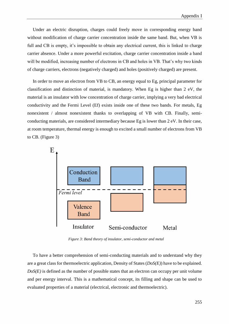
Appendix I
255
Under an electric disruption, charges could freely move in corresponding energy band
without modification of charge carrier concentration inside the same band. But, when VB is
full and CB is empty, it’s impossible to obtain any electrical current, this is linked to charge
carrier absence. Under a more powerful excitation, charge carrier concentration inside a band
will be modified, increasing number of electrons in CB and holes in VB. That’s why two kinds
of charge carriers, electrons (negatively charged) and holes (positively charged) are present.
In order to move an electron from VB to CB, an energy equal to Eg, principal parameter for
classification and distinction of material, is mandatory. When Eg is higher than 2 eV, the
material is an insulator with low concentration of charge carrier, implying a very bad electrical
conductivity and the Fermi Level (Ef) exists inside one of these two bands. For metals, Eg
nonexistent / almost nonexistent thanks to overlapping of VB with CB. Finally, semi-
conducting materials, are considered intermediary because Eg is lower than 2 eV. In their case,
at room temperature, thermal energy is enough to excited a small number of electrons from VB
to CB. (Figure 3)
To have a better comprehension of semi-conducting materials and to understand why they
are a great class for thermoelectric application, Density of States (DoS(E)) have to be explained.
DoS(E) is defined as the number of possible states that an electron can occupy per unit volume
and per energy interval. This is a mathematical concept, its filling and shape can be used to
evaluated properties of a material (electrical, electronic and thermoelectric).
Figure 3: Band theory of insulator, semi-conductor and metal

Appendix I
256
As explain before, in electron rich systems, energy levels are formed, separated by Eg, and
at 0 K, charge carriers fill the lowest level first, inside VB, while the highest filled energy state
is called the Fermi Level, Ef (electronic band above Ef is CB, separated by Eg). To described
the possibility of an electron to fill at a certain available level of these bands at an absolute
temperature T, Fermi-Dirac distribution f0(E) is used [9]:
𝑓0(𝐸) =1
1 + 𝑒𝐸−µ𝑘𝐵𝑇
(1)
where µ is the chemical potential (At T ≈ 0 K, µ = Ef)[10] and kB the Boltzmann constant.
Thanks to DoS(E), the number of available states that charge carriers can fill, and f0(E), the
probability of an electron to fill a state, this is possible to obtain the actual number of charge
carriers per volume in the system (N, also called carrier concentration or charge carrier density)
with the integral of their product. Hence, for T>0 and with energy E in the system [9–11]:
𝑁 = σ∫ 𝑓0(𝐸) . 𝐷𝑜𝑆(𝐸) 𝑑𝐸∞
0
(2)
N is one of the key parameter in order to tune properties of semi-conducting materials.
In previous part, it was explained that material can be classified (insulator, metal or semi-
conductor) based on its band gap, but DoS(E) have to be also considered. Band structures for
insulator, semi-metal, metal and semi-conductor are presented in Figure 4 [10,12].
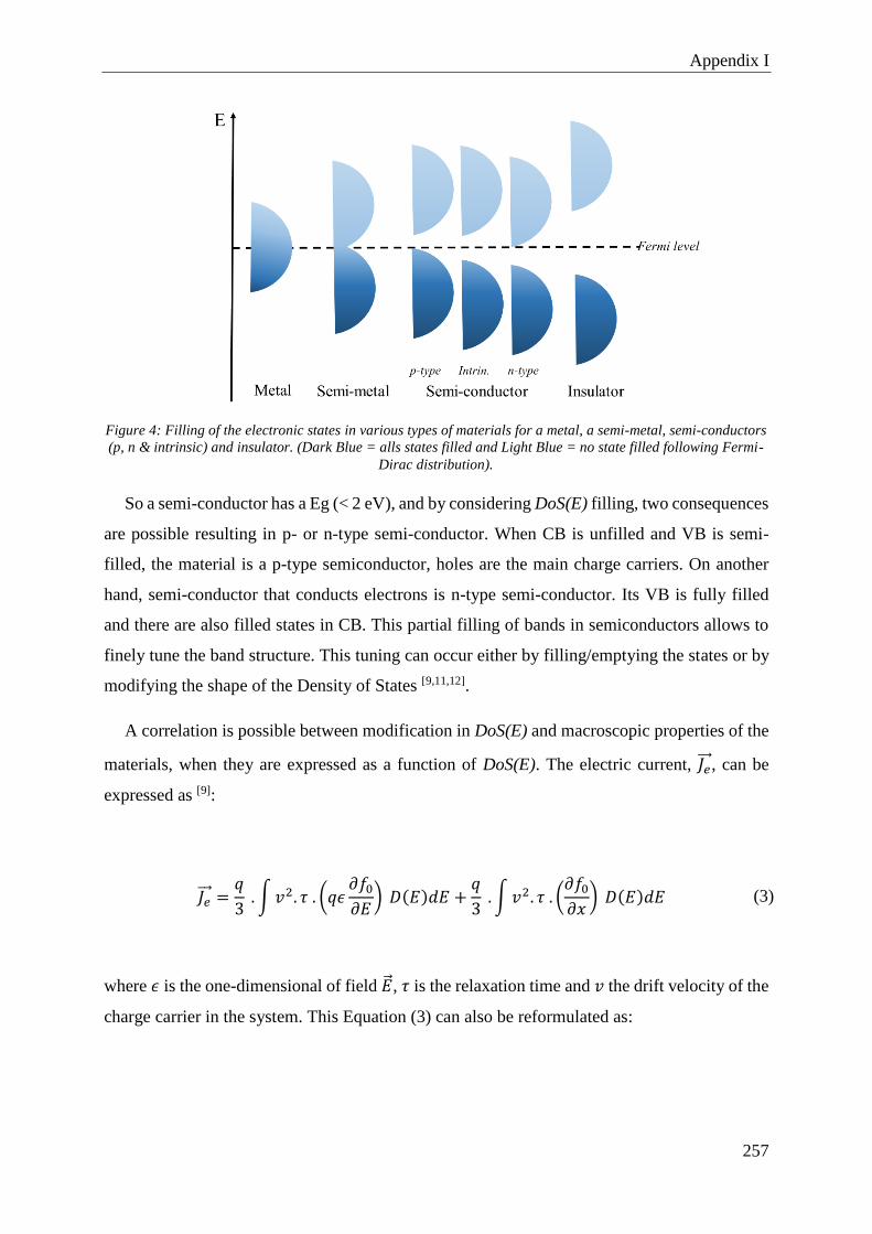
Appendix I
257
So a semi-conductor has a Eg (< 2 eV), and by considering DoS(E) filling, two consequences
are possible resulting in p- or n-type semi-conductor. When CB is unfilled and VB is semi-
filled, the material is a p-type semiconductor, holes are the main charge carriers. On another
hand, semi-conductor that conducts electrons is n-type semi-conductor. Its VB is fully filled
and there are also filled states in CB. This partial filling of bands in semiconductors allows to
finely tune the band structure. This tuning can occur either by filling/emptying the states or by
modifying the shape of the Density of States [9,11,12].
A correlation is possible between modification in DoS(E) and macroscopic properties of the
materials, when they are expressed as a function of DoS(E). The electric current, 𝐽𝑒 , can be
expressed as [9]:
𝐽𝑒 =𝑞
3 . ∫𝑣2. 𝜏 . (𝑞𝜖
𝜕𝑓0𝜕𝐸
) 𝐷(𝐸)𝑑𝐸 +𝑞
3 .∫𝑣2. 𝜏 . (
𝜕𝑓0𝜕𝑥
) 𝐷(𝐸)𝑑𝐸 (3)
where 𝜖 is the one-dimensional of field , 𝜏 is the relaxation time and 𝑣 the drift velocity of the
charge carrier in the system. This Equation (3) can also be reformulated as:
Figure 4: Filling of the electronic states in various types of materials for a metal, a semi-metal, semi-conductors
(p, n & intrinsic) and insulator. (Dark Blue = alls states filled and Light Blue = no state filled following Fermi-
Dirac distribution).
Appendix I
258
𝐽𝑒 = q . N . µ𝑒 . 𝜖 + 𝑞 . 𝑎 .𝜕𝑁
𝜕𝑥 (4)
where, N, is the carrier concentration as defined in Equation (2), µ𝑒 is the charge carrier mobility
(m²/Vs) and a is the carrier diffusivity (m²/s). Equation (4) is also called the drift-diffusion
equation [9]. In the first part of the relationship, the electrical conductivity can be identified as:
𝜎 = q . N . µ𝑒 (5)
where:
µ𝑒 =
𝑞3 . ∫ 𝑣2∞
0. 𝜏 . (
𝜕𝑓0𝜕𝐸
) . 𝐷(𝐸)𝑑𝐸
∫ 𝑓0∞
0(𝐸). 𝐷(𝐸)𝑑𝐸
(6)
Consequently, the electrical conductivity can be defined as:
𝜎 =𝑞
3 .∫ 𝑣2
∞
0
. 𝜏 . (𝜕𝑓0𝜕𝐸
) . 𝐷(𝐸)𝑑𝐸 (7)
The importance of the shape and the filling of the Density of States to material properties is
highlighted in the extracted relationships for electrical conductivity and charge carrier mobility.
Practically speaking, the electrical conductivity of a semiconducting material can be increased
either by increasing the carrier concentration (i.e. the filling the states) or by increasing the
carrier mobility. Considering that the carrier mobility is the measure of the mobile properties
of individual electrons in the system, tuning of μe can be achieved by modifications of the
material structure. For example, the mobility of an amorphous semiconductor is lower than the
mobility of a semi-crystalline or crystalline one as the amorphous material exhibits more
structural defects inhibiting the transport of electrons.
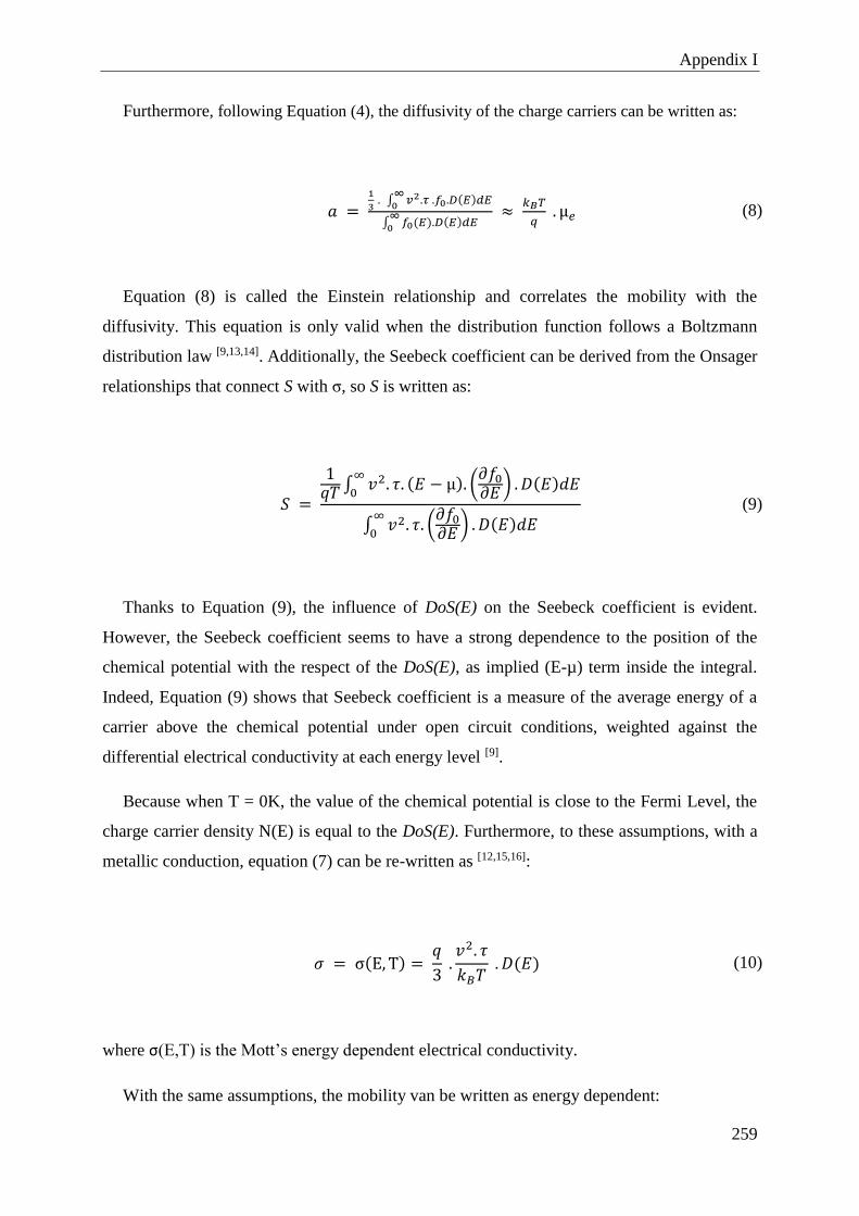
Appendix I
259
Furthermore, following Equation (4), the diffusivity of the charge carriers can be written as:
𝑎 = 1
3 . ∫ 𝑣2∞
0.𝜏 .𝑓0.𝐷(𝐸)𝑑𝐸
∫ 𝑓0∞0 (𝐸).𝐷(𝐸)𝑑𝐸
≈ 𝑘𝐵𝑇
𝑞 . µ𝑒 (8)
Equation (8) is called the Einstein relationship and correlates the mobility with the
diffusivity. This equation is only valid when the distribution function follows a Boltzmann
distribution law [9,13,14]. Additionally, the Seebeck coefficient can be derived from the Onsager
relationships that connect S with σ, so S is written as:
𝑆 =
1𝑞𝑇 ∫ 𝑣2. 𝜏. (𝐸 − µ). (
𝜕𝑓0𝜕𝐸
) . 𝐷(𝐸)𝑑𝐸∞
0
∫ 𝑣2. 𝜏. (𝜕𝑓0𝜕𝐸
) . 𝐷(𝐸)𝑑𝐸∞
0
(9)
Thanks to Equation (9), the influence of DoS(E) on the Seebeck coefficient is evident.
However, the Seebeck coefficient seems to have a strong dependence to the position of the
chemical potential with the respect of the DoS(E), as implied (E-µ) term inside the integral.
Indeed, Equation (9) shows that Seebeck coefficient is a measure of the average energy of a
carrier above the chemical potential under open circuit conditions, weighted against the
differential electrical conductivity at each energy level [9].
Because when T = 0K, the value of the chemical potential is close to the Fermi Level, the
charge carrier density N(E) is equal to the DoS(E). Furthermore, to these assumptions, with a
metallic conduction, equation (7) can be re-written as [12,15,16]:
𝜎 = σ(E, T) = 𝑞
3 .𝑣2. 𝜏
𝑘𝐵𝑇 . 𝐷(𝐸) (10)
where σ(E,T) is the Mott’s energy dependent electrical conductivity.
With the same assumptions, the mobility van be written as energy dependent:

Appendix I
260
µ𝑒(𝐸, 𝑇) =𝑞
3 .𝑣2. 𝜏
𝑘𝐵𝑇 (11)
And the diffusion coefficient:
𝑎 (𝐸, 𝑇) =1
3 . 𝑣2. 𝜏 (12)
Subsequently, the Seebeck coefficient is derived as:
𝑆 (𝐸, 𝑇) = 𝜋²
3 .𝑘𝐵²𝑇
𝑞 . (
𝜕ln (𝜎(𝐸))
𝜕𝐸)
𝐸=𝐸𝑓
(13)
which can be re-written as [12,15,16]:
𝑆 (𝐸, 𝑇) = 𝜋²
3 .𝑘𝐵²𝑇
𝑞 . ((
1
µ𝑒(𝐸, 𝑇). 𝜕(µ𝑒(𝐸, 𝑇))
𝜕𝐸)
𝐸=𝐸𝑓
+ (1
𝐷(𝐸, 𝑇) .
𝜕(𝐷(𝐸, 𝑇))
𝜕𝐸)
𝐸=𝐸𝑓
) (14)
So the Seebeck coefficient is analogous to [10,12,17]:
o The slope of the Density of States at Fermi Level
o The slope of the energy dependent “metallic” mobility at Fermi Level
Nevertheless, these relationships are only effective at T close to 0 K. When the temperature
starts to increase, the chemical potential is shifting away from the Fermi Level due to the
presence of defects in the material (e.g. structural defects). These defects modify the distribution
of carriers in the different states (i.e. the Fermi-Dirac distribution) [9,10]. As a result, the
Equations (10) - (14) are strictly valid at low temperatures close to 0 K and energies near the
Fermi position.
Appendix I
261
Conjugation
If it is energetically advantageous, atoms will bond together to from molecules. The atomic
orbitals overlap, sharing their electron density, forming bonds and as a consequence decreasing
the inter-atomic distance. Depending on the molecule formed, there are different types of
molecular bonds:
σ bonds are rotation symmetric with respect to the axis between the two participating atoms.
They are bonding orbital, stabilizing the molecule, with the shared electron density being
concentrated at the center between both atoms. The electron density for the corresponding
antibonding σ* orbitals with the same rotational symmetry is concentrated on opposite asides,
far away from the center between the two atoms. If one were to excite an electron from a σ
orbital to a σ* orbital, the bond between atoms would be cut, since the energy of the σ* orbital
lies above the ionization energy.
π bonds are weaker than σ bonds, since there is less overlap of the electron densities of the
participating atomic orbitals. The binding energy of a C=C double bond, which is composed of
one σ and one π bond, is less than twice that two σ bonds. This means, that an electron can be
excited from a filled π to an empty π* orbital without cutting the molecular bond.
Since π-conjugation is formed between the overlap of out-of-plane p-orbitals, this requires
the molecule to be planar. The molecule is rigid and cannot arbitrarily bend, or rotate along the
bond axis without breaking the π bonds.
This part will be focused on π-conjugated polymers. In this system, the electrons of the
carbon molecules of the units are delocalized in an extended π-system due to the double bonds.
The semi-conducting behavior, in π-conjugated polymer results from this delocalization and
express the electronic properties of the material. So, π-bonds where the electrons are delocalized
are the Highest Occupied Molecular Orbital (HOMO) of the material and the π*-anti-bonds are
the Lowest Unoccupied Molecular Orbital (LUMO). In contrary with organic substance, like
ethylene or benzene molecule, where the band gap is too large (insulating material), for a
conjugated polymer, the extension of each π-π* bond results in the recombination of π-orbitals.
This is transcribed by an addition of states to the HOMO and the LUMO, resulting in a reducing
of the band gap and semi-conducting behavior [11,18,19].

Appendix I
262
For example, the simplest π-conjugated polymer (Polyacetylene), is intrinsically a semi-
conducting material thanks to its alternated π-bonds. By treating this polymer with oxidative
iodine vapors, radical ions rea formed on the chain, so called solitons, adding more states to the
HOMO-LUMO levels, inducing an even more decrease of the band gap. In this state,
Polyacetylene shows a high electrical conductivity with a metallic behavior [20–22].
On another side, other π-conjugated polymers, like polythiophenes, are not intrinsically
semiconducting and must be doped in order to obtain a semiconducting behavior. The reason
of this behavior is due to a localization of the electrons in the π-orbitals of a units. So, chains
are oxidized (an electron is taken for p-doped polymer), or reduced (an electron is given for n-
doped polymer), in order to improve the delocalization of electrons by changing the thiophene
rings configuration to the quinoid form (Figure 5). Consequently, the newly formed double
bonds enable the recombination of the π-orbitals, extending the π-system along the chain, and
so the charge carriers (holes and electrons) are more easily delocalized, reducing the band gap
(semi-conducting behavior achieved) [11,19,23,24].
S S
n n
Aromatic Quinoid
Figure 5: Aromatic to Quinoid form for thiophene
The new charge carriers formed in these “extrinsically” semi-conducting polymers are called
polarons or bipolarons. Polaron are due to a chain conformation changes from the aromatic to
quinoid form, during the doping, inducing a chain lattice relaxation. Polaron assists in the
extension of the π-system (Figure 6). As a result, electronic states are added in the HOMO and
LUMO levels (Figure 7), and are referred to polaron bands [19,23,25].
Figure 6: Formation of a polaron (center) and a bipolaron (right) for an oligothiophene
S
S
S S
S
S S
S
S-e--e-

Appendix I
263
By increasing the doping, multiple polarons (on the same chain) aren’t formed in the π-
systems, in place a bipolaron is spontaneously created (Figure 7). A bipolaron is an extended
lattice relaxation that gives an energy to the system, which is larger than the repulsion between
the two ions. That’s why, this is thermodynamically more favorable to form a new polaron
besides the already existing polaron of the chain, than to anywhere else in the chain. Thus, a
bipolaron band of higher energy is created, and by increasing dopant concentration, number of
bipolatons is also increased, forming a widened bipolaron bands in the material (Figure 8) [25,26].
Density of states of the polymer is constituted by all these electronic states, solitons, polarons
or bipolarons, filling it with redox processes. When dopant concentration is low, Dos of the
polymer is comparable to a conventional inorganic semi-conductor. By increasing the doping
rate, so decreasing the band gap, the polymer DoS tend to resemble to a metal or semi-metal,
where the HOMO is the work function of the material [25,26].
Figure 7: Band structure of one polaron (left), two polarons (center) and one bipolaron (right)
Figure 8: Evolution of the band structure for a conjugated polymer upon doping: low doping level, polaron
formation (left), moderate doping level, bipolaron formation , high doping level, formation of bipolaron bands

Appendix I
264
The formation of those new energy bands, results in band transport mechanism of the charge
carrier between the different energy bands in the polymer. Although, polymers are not perfect
crystal, and do not have prerequisites to band transport, so the main charge transport mechanism
is a thermally activated hopping transport. Charge carriers “hop” between the different units in
an inter-chain (green arrow) and intra-chain (red arrow) level (Figure 9). These hopping sites
are the extended π-systems formed between the chain units, which are inherent conducting
[11,24,27,28].
Figure 9: Hopping trnasport in a conducting polymer with low (left) and high (right) degree of crystallinity. Red
arrows show the hopping transport intra-chains and green arrows show the hopping transport inter-chains. Blue
blocks are crystalline parts and blue lines amorphous part of the conducting polymers.
These conducting formations are called “metallic” island and are dispersed inside the
amorphous matrix [28]. The distribution of these metallic islands in amorphous matrix heavily
affects the shape of the Density of States. So, the electronic structure and properties of doped
polymer materials are highly dependent on the structural properties such as the degree of
crystallinity and the chain orientation. When the degree of crystallinity is high, π-orbitals can
recombine to extended π-system, and larger “metallic islands” are formed in the amorphous
matrix making charge carrier more mobile. Also, a higher conjugation length benefits the intra-
chain hopping transport. For the inter-chain, the hopping transport occurs either to level of the
chain backbone or out-of-normal to the polymer backbones. This configuration is better for
charge transport because π-orbitals are at a closer distance leading to an increased hopping the
sites. Finally, in a conductor polymer, when all structural parameters are respected at the intra-
and inter-chain level, π-orbitals can recombine into an extended π-system, called a “bipolaron
network” (Figure 10) [29].

Appendix I
265
Now, this conformation of a “bipolaron network”, is an ideal conformation for
thermoelectricity, because its benefits the Seebeck coefficient of the material. Thanks to the
Mott’s equation (Equation (13)), Seebeck coefficient is analogous to the slope of the DoS at the
Fermi Level. In a doped conducting polymer with a “bipolaron network”, the band edge is
broader due to the extended π-system. Hence, the slope of the DoS at Fermi Level is steeper
and the Seebeck coefficient of the material is higher.
Doping levels of the material have to be considered for thermoelectric optimization.
Increasing the carrier concentration will add more states to the HOMO, narrowing the band
gap, thus the slope of the DoS will be decreased, inducing a lower Seebeck coefficient. So, in
order to achieve high thermoelectric performance, proper and detailed material design is needed
[27].
In the case of highly conducting systems, like PEDOT, the electrical conductivity follows
the thermally activated variable range hopping (VHR) model, proposed by Mott (Equation (15))
[12,28]:
𝜎 = 𝜎𝑜 . 𝑒−(
𝑇0 𝑇
)𝑝
(1519)
Figure 10: A « bipolaron network ». A semi-crytalline doped polymer (bipolarons as charge carriers) on top. The
same polymer represented with the π-orbitals of individual doped conjugated chains in blue (left). Then with
increasing the crystallinity of the same polymer, the various π-orbitals overlap with a much wider π-systems, a
bipolaron network (on right).
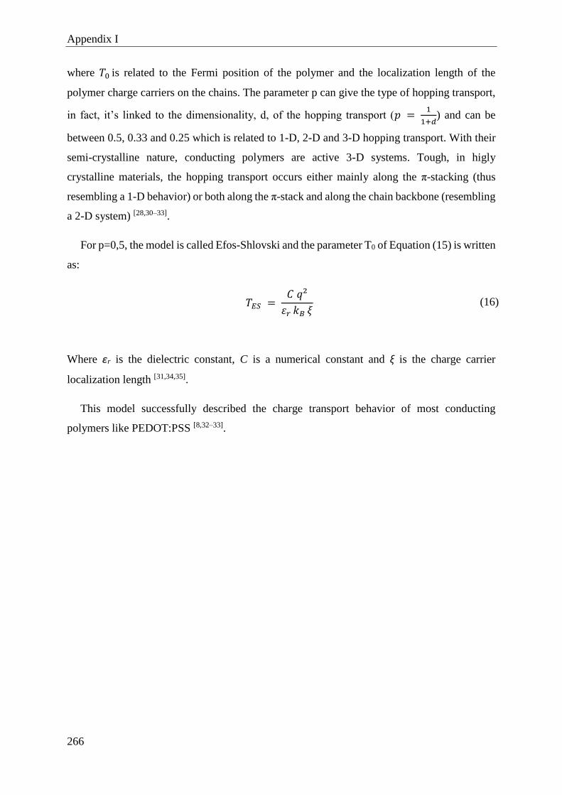
Appendix I
266
where 𝑇0 is related to the Fermi position of the polymer and the localization length of the
polymer charge carriers on the chains. The parameter p can give the type of hopping transport,
in fact, it’s linked to the dimensionality, d, of the hopping transport (𝑝 = 1
1+𝑑) and can be
between 0.5, 0.33 and 0.25 which is related to 1-D, 2-D and 3-D hopping transport. With their
semi-crystalline nature, conducting polymers are active 3-D systems. Tough, in higly
crystalline materials, the hopping transport occurs either mainly along the π-stacking (thus
resembling a 1-D behavior) or both along the π-stack and along the chain backbone (resembling
a 2-D system) [28,30–33].
For p=0,5, the model is called Efos-Shlovski and the parameter T0 of Equation (15) is written
as:
𝑇𝐸𝑆 = 𝐶 𝑞²
𝜀𝑟 𝑘𝐵 𝜉 (16)
Where εr is the dielectric constant, C is a numerical constant and ξ is the charge carrier
localization length [31,34,35].
This model successfully described the charge transport behavior of most conducting
polymers like PEDOT:PSS [8,32–33].

Appendix I
267
C PEDOT:Tos formation mechanism
S
O O
HH
Fe(Tos)3
- e -S
O O
HH
+
S
O O
HH
S
O O
HH S
OO
H H
S
O O
HS
OO
H
H
H
S
O O
HS
OO
H
H
H S
O O
HS
OO
H
- 2 H+
Tos-
Tos-Tos-
Tos-
Tos-
Tos-
Tos-
Tos- : S
O
O
O
+ 2 TosH
S
O O
S
OO
S
OO
S
O O
S
O O
S
OO
S
OO
S
O O
Fe(Tos)3
Tos-
S
O O
S
OO
S
OO
S
O OTos-
Fe(Tos)3
Tos-
Figure 11: Polymerization mechanism of EDOT in presence of Fe(Tos)3.

Appendix I
268
References
[1] J. C. A. Peltier, Nouvelles Experiences sur la Caloricite des Courans Electriques,
Paris, First separate edition, reprinted from Annales de Chimie et de Physique, LVI,
1834, pp. 371–386.
[2] W. Thomson, Proc. R. Soc. Edinb. 1857, 3, 91.
[3] Henry Crew, General Physics: An Elementary Text-book for Colleges; Third Edition,
The Macmillan company, 1916.
[4] Leon van Dommelen, A.11 Thermoelectric effects, FAMU-FSU College of
Engineering, view on:
http://www.eng.fsu.edu/~dommelen/quantum/style_a/nt_pelt.html (July, 2019).
[5] R. F. Pierret, Semiconductor Device Fundamentals., 2nd Edition, Volume VI, Pearson,
2002 (ISBN 10: 978-0130617927).
[6] P.S. Kireev, Semiconductor Physics, Central Book Ltd, 1978, (ISBN
13:9780714712321).
[7] S. M. Sze and K. NG. Kwok, Physics of Semiconductor Devices, 3rd Edition., Wiley,
2006, (ISBN :978-0-470-06830-4).
[8] R. F. Pierret, Semiconductor Device Fundamentals. « 2nd Edition », Addison-Wesley,
1996 (ISBN 10: 978-0201543933).
[9] G. Chen, Nanoscale Energy Transport and Conversion: A Parallel Treatment of
Electrons, Molecules, Phonons, and Photons; MIT-Pappalardo Series in Mechanical
Engineering; Oxford University Press: Oxford, New York, 2005.
[10] N. Ashcroft, N. D. Mermin, Solid State Physics, Brooks/Cole, 1976 (ISBN 10:
0030493463)
[11] M. Geoghegan, G. Hadziioannou, Polymer Electronics., Oxford Master Series in
Physics, 2013, (ISBN: 9780199533824)
[12] N. Mott, E. A. Davis, Electronic Processes in Non-Crystalline Materials, Oxford
Classic Texts in the Physical Sciences, Oxford University Press: Oxford, New York,
2012.
[13] G. A. Wetzelaer, L. J. Koster, P. W. Blom, Phys. Rev. Lett., 2011, 107, 066605.
[14] S. Xiao-Hong, S. Jiu-Xun, X. Chun-Hua, Org. Electron. 2016, 35, 65.
[15] M. Cutler, N. F. Mott, Phys. Rev. 1969, 181, 1336.
[16] M. Jonson, G. D. Mahan, Phys. Rev. B 1980, 21, 4223.
[17] S. Ihnatsenka, X. Crispin, I. V. Zozoulenko, Phys. Rev. B 2015, 92, 035201.
[18] Y. W. Park, A. J. Heeger, M. A. Druy, A. G. MacDiarmid, The Journal of Chemical
Research, 1985, 18, 309-315.
[19] J. L. Brédas, F. Wudl, A. J. Heeger, Solid State Communications, 1987, 63, 577-580.
[20] R. E. Peierls, R. Peierls, Surprises in Theoretical Physics; Princeton University Press,
1979.
[21] A. J. Heeger, Rev. Mod. Phys. 2001, 73, 681.
[22] C. K. Chiang, C. R. Fincher, Y. W. Park, A. J. Heeger, H. Shirakawa, E. J. Louis, S.
C. Gau, A. G. MacDiarmid, Phys. Rev. Lett. 1977, 39, 1098.
[23] J. L. Brédas, B. Thémans, J. G. Fripiat, J. M. André, R. R. Chance, Phys. Rev. B 1984,
29, 6761.
[24] V. Coropceanu et al., Charge Transport in Organic Semiconductors, 2007, 107 926-
952.
[25] R. R. Chance, J. L. Brédas, R. Silbey, Phys. Rev. B 1984, 29, 4491.
[26] J. L. Brédas, G. B. Street, Accounts of Chemical Research, 1985, 18, 309-315.

Appendix I
269
[27] O. Bubnova, X. Crispin, Energy Environ. Sci. 2012, 5, 9345.
[28] A. B. Kaiser, V. Skákalová, Chem. Soc. Rev. 2011, 40, 3786.
[29] O. Bubnova, Z. U. Khan, H. Wang, S. Braun, D. R. Evans, M. Fabretto, P. Hojati-
Talemi, D. Dagnelund, J.-B. Arlin, Y. H. Geerts, S. Desbief, D. W. Breiby, J. W.
Andreasen, R. Lazzaroni, W. M. Chen, I. Zozoulenko, M. Fahlman, P. J. Murphy, M.
Berggren, X. Crispin, Nat. Mater. 2014, 13, 190.
[30] A. N. Aleshin, R. Kiebooms, A. J. Heeger, Synth. Met. 1999, 101, 369.
[31] B. Skinner, T. Chen, B. I. Shklovskii, Phys. Rev. B, 2012, 85, 205316.
[32] A. J. Kronemeijer, E. H. Huisman, I. Katsouras, P. A. van Hal, T. C. T. Geuns, P. W.
M. Blom, S. J. van der Molen, D. M. de Leeuw, Phys. Rev. Lett. 2010, 105, 156604.
[33] J. J. Brondijk, W. S. C. Roelofs, S. G. J. Mathijssen, A. Shehu, T. Cramer, F. Biscarini,
P. W. M. Blom, D. M. de Leeuw, Phys. Rev. Lett. 2012, 109, 056601.
[34] T. Chen, K. V. Reich, N. J. Kramer, H. Fu, U. R. Kortshagen, B. I. Shklovskii, Nat.
Mater. 2016, 15, 299.
[35] A. L. Efros, B. I. Shklovskii, J. Phys. C Solid State Phys. 1975, 8, L49.
[36] K. Lee et al., Nature, 2006, 441, 65-68.
[37] A. N. Aleshin, Phys. Solid State 2010, 52, 2307.
[38] S. Bhadra, N. K. Singha, D. Khastgir, Journal of Applied Polymer Sciencei, 2007, 104
(3), 1900-1904.

270

Appendix II
271
Appendix II:
Material and methods

Appendix II
272
A Chemical materials
Iron(III) p-toluenesulfonate at 40wt% in 1-butanol (named Clevios CB 40 V2) was
purchased from Heraus. PCBM was purchased from Solaris (99+%). F4TCNQ was purchased
from TCI chemicals. All others chemical compounds, additives and solvents were purchased
from Sigma Aldrich. All chemicals were used as received unless otherwise stated.
PNDIBS were received from Prof. Samson Jenekhe’s group (University of Washington).
B Polymer synthesis
PEDOT:Tos formulations
o High boiling point solvent formulation:
500 µL of a high boiling point solvent is added to 10 mL of oxidant solution, iron(III) tosylate
in 1-butanol (40 wt%). Volume fraction of solvent additive is 5 % v/v with respect to the
solution volume. The solution is stirred 12h at room temperature and stored at 4°C.
o Pyridine formulation:
0,5 eq. of pyridine are added to 1 eq. of oxidant solution, iron(III) tosylate in 1-butanol
(40 wt%). The solution is stirred 12h at room temperature and stored at 4°C.
High boiling point solvent and pyridine formulation:
300 µL of pyridine is added to 10 mL of oxidant solution, iron(III) tosylate in 1-butanol
(40 wt%). Then 300 µL of high boiling point solvent is added to the previous mixture. Volume
fraction of each additive is 3 % wt with respect to the solution volume. The solution is stirred
12h at room temperature and stored at 4°C.
o In-situ oxidative polymerization of EDOT:
Polymerization directly takes place during the film process. 9,9 µL of EDOT were added to
300 µL of a previous oxidative formulation (Oxidant/monomer ratio = 2.3 / 1.2 eq.) The mixture
was stirred 30 s before processing. On cleaned / treated substrate (see Substrate cleaning /
treating procedure), oxidant/EDOT mixture, filtered with 0,45 µm PTFE filter, was spin-coated
at 1500 rpm for 30 s with a ramp of 800 rpm/s². The resulted thin films were annealed on a hot
plate (100°C) in ambient conditions for 15 min. Afterwards, the film was sequentially washed
with two 1-butanol bath and one ethanol bath during 5 min per bath. The role of the bathing

Appendix II
273
steps is to remove the unreacted and insulating oxidant that remained after the end of the
polymerization. Considering that the Fe(Tos)3 used in the synthesis was dissolved in n-butanol,
this solvent is chosen as a first bathing step. The second and third bathing steps are added to
further remove any remaining oxidant. After the bathing steps, the films are dried with Nitrogen
gas flow.

Appendix II
274
P3HT synthesis procedure
Figure 1: Poly(3-hexylthiophène)
Bulk made P3HT was synthesized according to the literature [1].
2,5-dibromo-3-hexylthiophene (0.5g, 1.5 mmol) [116971-11-0] were dissolved in 15 mL
anhydrous THF in a 50 mL three-necked flask. A 2 mol/L solution of t-butylmagnesium
chloride (0.75 mL, 1.5 mmol) [677-22-5] in diethyl ether was added via a purged syringe, and
the reaction mixture was gently refluxed for 90 min. The reaction mixture was allowed to cool
to room temperature, and Ni(dppp)Cl2 (0.013 g, 0.023 mmol) [15629-92-2] was added to the
reaction mixture. The polymerization was left to proceed under stirring for 15 min at room
temperature and then quenched with degassed methanol. The reaction mixture was then
concentrated by rotary evaporation (0.23 g, 89% yied). GPC: Mn = 20600 g/mol
(Mn/Mw = 1.26). 1H NMR (400 MHz, CDCl3, ppm) : 6.98 (s, 1H), 2.80 (t, 2H), 1.69 (t, 2H),
1.43-1.35 (m, 6H), 0.9 (t, 3H).

Appendix II
275
PCDTBT synthesis procedure
Figure 2: PCDTBT
Bulk made PCDTBT was synthesized according to the literature [2].
2,7-bis(4,4,5,5-tetramethyl-1,3,2-dioxaborolan-2-yl)-N-9-heptadecanyl-carbazole (654.4 mg,
0.966 mmol) [958261-51-3], 4,7-di(2-bromothien-5-yl)-2,1,3-benzothiadiazole (458.8 mg,
1 mmol) [288071-87-4], tris(dibenzylidedeneacetone)dipalladium(0) (4.2 mg, 0.0046 mmol)
[51364-51-3] and tri(o-tolyl)phosphine (6.1 mg, 0.020 mmol) [6163-58-2] were dissolved in
3.4 mL (NH4OH)aq and 10 mL toluene in a 25 Schlenk tube. The reaction mixture was stirred
at 95°C for 3 hours (temperature ramp of 5°C/5min). Then 110 µL of bromobenzene [108-86-
1] were added and reacted for an hour. Finally, 120 mg of phenylboronic acid [98-80-6] in 3mL
of toluene were added and reacted for another hour. The resulting mixture was precipitated into
a mixture of methanol (100 mL) / water (10 mL). The precipitate was washed by Soxhlet
extraction with acetone for one night followed by a day with heptane and then extracted with
CHCl3. The CHCl3 portion was concentrated and washed with 500 mL of cold methanol,
collected and dried in vacuum. A deep purple powder (2,25g, 90% yield). GPC:
Mn = 27649 g/mol (Mn/Mw = 2.19). 1H NMR (400 MHz, CD2Cl2, ppm): 8.3-7.1 (br, 12H,
ArH); 4.74 (br, 1H); 2.40 (br, 2H); 2.04 (br, 2H); 1.45-1.23 (br, 8H); 1.23-1.00 (br, 16 H); 0.78
(br, 6H).

Appendix II
276
PTB7 synthesis procedure
Figure 3: PTB7
Bulk made PTB7 was synthesized according to the literature [3,4].
2,6-Bis(trimethyltin)-4,8-bis(2-ethylhexyl)benzo[1,2-b:3,4-b’]dithio-phene (386 mg,
0.50 mmol) [1160823-78-8] and 2-ethylhexyl-4,6-dibromo-3-uorothieno[3,2-c]thiophene-2-
carboxlate (236 mg, 0.50 mmol) [1237479-38-7] were dissolved in 8 mL toluene and 4 mL
dimethylformamide in a 25 mL Schlenk tube. Tetrakis-(triphenyl-phosphine)palladium(0)
(25 mg, 0.05%mol.) [14221-01-3] was added and the reaction mixture was stirred at 120°C for
24 hours. The resulting mixture was poured into methanol (80 mL). The precipitate was washed
by Soxhlet extraction with acetone for one day followed by a further day with heptane, and then
extracted with CHCl3. The CHCl3 portion was concentrated, a deep blue powder (322 mg, 86%
yield). GPC: Mn = 41567 g/mol (Mn/Mw = 2.26). 1H NMR (400 MHz, CDCl2CDCl2, ppm):
7.01-6.64 (br, 2H, ArH); 3.77-3.60 (br, 6H); 1.26-0.36 (br, 45H).

Appendix II
277
Substrates references
5.1 Glass substrates
Two kinds of glass substrates were used. The first one, Microscope slides washed, degreased,
with raw edges from RS France (purchased on Fischer scientific) were used for Seebeck
coefficient and 2-probes electrical measurement (described below). The other one, Microscope
slides of 1,5 cm per 1,5 cm were used for 4-point probe resistivity measurement (described
below).
5.2 Silicon substrates
Supplier Type/dopant Resistivity
(ohm.cm)
Diameter
(mm)
Thickness
(µm) Orientation Surface Grade
Sil’tronix
P - Boron 20 150 675 +/- 25 <100> polished Prime
CZ
N-
Phosphorus 20 150 675 +/- 25 <100> polished
Prime
CZ
P - Boron 1.5 150 675 +/- 25 <100> polished Prime
CZ
N-
Phosphorus 1.5 150 675 +/- 25 <100> polished
Prime
CZ
P - Boron 0.05 150 675 +/- 25 <100> polished Prime
CZ
N-
Phosphorus 0.05 150 675 +/- 25 <100> polished
Prime
CZ
Si-Mat
P - Boron 0.025 100 525 +/- 25 <100> polished Prime
CZ
N - Antimony 0.025 100 525 +/- 25 <100> polished Prime
CZ
Table 1: Commercial characteristics of silicon wafers

Appendix II
278
C Material processing
Substrate cleaning and treatment:
All glasses and silicon substrates were washed in ultrasonic baths of ethanol, isopropanol
and acetone for 15 mn per washing step. Then substrates were treated by UV-O3 for 20 min
before film processing.
P3HT
2.1 Mixed-solution doping
P3HT solutions (20 mg/mL) and the dopant, F4TCNQ solutions (1 mg/mL) in chlorobenzene
were heated to 80°C and left dissolve overnight. The mixed-solutions, P3HT:F4TCNQ, were
prepared immediately prepared before spin-coating. F4TCNQ was added at 60°C to give final
solutions at 10 mg/mL. 50 nm thin films, were obtained via spin-coating at 2000 rpm during
60s (acceleration speed set at 800 rpm/s²). Films were annealed on a hot plate at ≈80 °C for six
hours.
2.2 Sequential doping
P3HT thin films were prepared by spin-coating previous P3HT solution (10 mg/mL, CB) to
form 50 nm thin films. Doping was performed via sequential doping process, P3HT film were
wetted with F4TCNQ at different concentration in acetonitrile. After 30s, the excess was
remove by spin-coating at 1000 rpm. Films were annealed on a hot plate at ≈80 °C for six hours.
PCDTBT
PDTBT solutions (50 mg/mL) in chlorobenzene were heated to 80°C and left dissolve
overnight. FeCl3/chloroform solutions at different concentration were dropped wise into
PCDTBT/chloroform solution to obtain final solution at 10 mg/mL. Solution were stirred at
least 10 min, then spin-coated 2000 rpm during 60s (acceleration speed set at 800 rpm/s²) to
form approximately 50 nm thin film. Films were annealed on a hot plate at ≈80 °C for six hours.

Appendix II
279
PTB7
PTB7 solutions (10 mg/mL) in 1,2,4-trichlorobenzene (TCB) were heated to 80 °C and left
dissolve overnight. For solutions containing 1,8-diiodooctane (DIO), 15 mg of PTB7 were
dissolved in a mixture of 970 µL of TCB and 30 µL of DIO, and stirred for at least 12 hours at
80°C. 50 nm thin films, were obtained via spin-coating at 2200 rpm during 60s (acceleration
speed set at 1000 rpm/s²). Films were annealed on a hot plate at ≈120 °C for six hours.
PCBM
PCBM solutions (40 mg/mL) in chlorobenzene were heated to 80°C, and stirred one day.
The mixed-solutions, PCBM:N-DPBI, were prepared immediately prepared before spin-
coating. 5wt% of N-DPBI were added to a PCBM solution of 10 mg/mL. Then, various amount
of AOB were added to this solution at 80°C. 50 nm thin films, were obtained via spin-coating
at 2000 rpm during 60s (acceleration speed set at 800 rpm/s²) in a glovebox. Films were
annealed on a hot plate at ≈80 °C for six hours.
PNDBIS
PNDBIS and the molecular dopants N‐DMBI were dissolved in 1,2‐dichlorobenzene (DCB)
at a concentration of 10 mg/ml. PNDBIS solutions were heated at 80 °C and stirred for 1 hour.
Dopants were used unheated within 12 hours of dissolution. Aliquots of dopant and polymer
solution were mixed at room temperature to achieve the dopant concentrations reported. Films
were spin cast from solutions described above onto substrates described in the section in a
glovebox at 2000 rpm for 60 s. Films were annealed on a hot plate at ≈120 °C for six hours in
the glovebox.
General comment
During the study of the thermoelectric properties as a function of the thickness of the organic
materials, the following protocol was applied to vary the thickness. This protocol was valid for
P3HT, PCDTBT, PTB7, PCBM and PNDIBS. Up to 250 nm thick films, the concentration of
the deposited solution, as well as the spin-coating speed, were modified to achieve the desired
thickness. In the case of thicker films, the method of drop-casting was chosen, the same
proportion and concentration were kept.
PEDOT:Tos layer stacking was easier. In fact, the resulting thin film obtained with the
previously described protocol is insoluble. So, after the washing step, another PEDOT:Tos

Appendix II
280
deposition was directly realized on PEDOT:Tos thin films. Each polymer layer adds 50 nm
approximately.

Appendix II
281
D Device architecture
Substrate cleaning
All glasses and silicon substrates were washed in ultrasonic baths of ethanol, isopropanol
and acetone for 15 mn per washing step.
Then, only on silicon substrate, a supplementary step was required before electrode
deposition in order to remove the native oxide (SiO2). Following the RCA procedure, silicon
substrates were putted in different baths:
o Standard Clean (SC-1): 5 parts of deionized water, 1 part of ammonia water (29% wt of
NH3 in water) and 1 part of H2O2 (30% wt in water) at 80°C for 10 min;
o Oxide strip: 1 part of HF (49% wt) in 50 parts of water for 2 min;
o Standard Clean (SC-2): 6 parts of deionized water, 1 part of HCl (37% wt in water) and
1 part of H2O2 (30% wt in water) at 80°C for 10 min.
o Oxide strip: 1 part of HF (49% wt) in 50 parts of water for 2 min;
o Rinsing: Deionized water;
o Drying: Nitrogen flux (filtered).
Devices for Seebeck coefficient and electrical
conductivity measurement:
On clean glass or silicon substrate, 10 nm of chromium and 100 nm of gold were deposited
by Physical Vapor Deposition (PVD) thanks to a metal evaporator, Lesker Mini Spectros. The
device configuration and dimensions are presented in Figure 4.
3 cm
2 cm 0.5
cm
1.5 cm : Cr/Au electrodes
: glass or silicon substrate
Figure 4: Schematic representation of devices for Seebeck coefficient and electrical conductivity measurement.

Appendix II
282
Polymer thin films were deposited on top of this device, and half of the polymer film on the
electrode was washed out, in order to make it appear. An example with final devices of
PEDOT:Tos stacking on silicon is presented below in Figure 5:
Figure 5: Picture of devices for Seebeck coefficient and electrical conductivity measurement coated with
PEDOT:Tos. From left to right are presented bare silicon to 7 layers of PEDOT:Tos.
Thermoelectric generator
Thermoelectric converters were fabricated for demonstration of the phenomena reported in
this study. Fabrication steps are described in Figure 6. First, similar devices than devices for
Seebeck coefficient and electrical conductivity measurement were used for thermoelectric legs
(Figure 6a). Various polymer and organic materials were deposited on top of these devices
(Figure 6b). The substrate was either glass or doped silicon. The polymer + substrates were then
cut with diamond cutter in dimensions 25 mm x 3mm, following dashed lines. As previously,
half of the polymer film on the electrode was washed out, in order to make it appear. P-n-p legs
junctions were stuck with glue on top of a glass substrate, and the connection between the legs
was being made by carbon paste (Figure 6c). Example of TEGs are showed in the main
manuscript part about TEGs.
Figure 6: Schematic representation of fabrication steps for three-legs TEG.
(a) (b) (c)
P P N

Appendix II
283
In case of flexible TEGs, 100 µm thick flexible PET sheets were used. First, the organic
material was deposited, following the previous protocol cited (Material processing section), on
a small PET sheet of 25 mm x 30 mm. The organic material on PET was then cut with scissors
in dimensions 25 mm x 3mm. Then, p-n-p legs junctions were stuck with glue on top of another
larger PET substrate. Finally, the electrodes and connections between the legs was being made
by silver paste (Figure 7).
Figure 7: Pictures of p-n-p-n-p 5-legs thermoelectric generator with p-type and n-type legs coated with one
layer of PCDTBT and PCBM on PET substrate.
P-type legs are made with PCDTBT and n-type legs are made with PCBM.

Appendix II
284
E Silicon etching
Silicon substrates used in this study are described in a previous section named Substrates
references. All experiments were performed at room temperature unless contraindicated.
Following the RCA procedure, silicon substrates were washed in different baths before each
etching process:
o Standard Clean (SC-1): 5 parts of deionized water, 1 part of ammonia water (29% wt of
NH3 in water) and 1 part of H2O2 (30% wt in water) at 80°C for 10 min;
o Oxide strip: 1 part of HF (49% wt) in 50 parts of water for 2 min;
o Standard Clean (SC-2): 6 parts of deionized water, 1 part of HCl (37ù wt in water) and
1 part of H2O2 (30% wt in water) at 80°C for 10 min.
o Oxide strip: 1 part of HF (49% wt) in 50 parts of water for 2 min;
o Rinsing: Deionized water;
o Drying: Nitrogen flux (filtered).
Preface
It’s important to note that visual evaluation of the reflectivity gives a clue to the good
realization of the etching process. In fact, Figure 8 compares bare silicon, silicon pyramids,
porous silicon, and silicon nanowires. For nanostructured silicon, the mirror effect is lost, and
the substrate turns black for the SiNWs.
Figure 8: Picture of 1.5 cm x 1.5 cm silicon substrate.
Different etching treatment were applied from left to right, bare silicon, KOH etching, soft MACE and regular
MACE.
Bare silicon Silicon
pyramids
Porous
silicon
Silicon
Nanowires

Appendix II
285
Silicon nanowires
MACE process was applied to silicon substrates and various parameters such as noble metal
nature and concentration, etching time and HF/oxidant ratio were studied in order to obtain
silicon nanowires for all silicon substrates with different doping concentration. Step by step
experiments were carried out. Only one parameter was changed for each study, the others were
set to the values shown in Figure 9, thus comparable experiments were done.
In Figure 9, each colour corresponds to a specific bath, and the text writes under it are
compounds names mixture, purity or concentration, and the ratio between species, respectively.
Time in each bath is written inside the bath schematic. Two routes were followed, the first one
with deposition of the noble metal through a wetting process. The other route was the deposition
of the noble metal directly on the silicon substrate via Physical Vapour Deposition (PVD).
Figure 9: Schematic representation of regular MACE procedure.
Finally, the best procedure in order to obtain regular silicon nanowires are resumed below
in Figure 10. Each bath was used only one time, after it was replaced. The last step, unmarked,
was treated silicon nanowires with HF to remove the oxide layer. Unfortunately, this last step
made the surface hydrophobic. So, in order to successfully deposited the PEDOT:Tos on top of
SiNWs, this last step wasn’t performed. Furthermore, during the PEDOT:Tos spin-coating,
before the spin-cast starting, the solution (monomer with oxidant) was let 30 s on the substrate.
Figure 10: Schematic representation of optimized MACE procedure

Appendix II
286
Porous silicon
MACE process was applied to silicon substrates, and porous silicon was obtained as a side
product of silicon nanowires. So the procedure Figure 11 was followed:
Figure 11: Schematic representation of regular soft MACE procedure
Silicon pyramids
KOH etching was applied to silicon substrates, isopropyl alcohol concentration, potassium
hydroxide concentration and etching time were studied in order to obtain silicon pyramids for
all silicon substrates with different doping concentration. Step by step experiments were carried
out. Only one parameter was changed for each study, the others were set to the values shown
in Figure 12, thus comparable experiments were done. Etching procedure was carried out in a
beaker at 80°C under agitation. A home-made clamp system allowed to put three samples at the
same time. The final step was a washing procedure with deionized water.
Figure 12: Schematic representation of the set up for KOH/IPA etching process.
General comment
Substrates with electrodes have also been etched with the previously described procedures.
Except, gold can serve as a catalyst for these processes, and therefore can be degraded by them.
Protection was, therefore, necessary, a Kapton tape was used to protect the different electrodes
during engraving. No degradation was then noted.
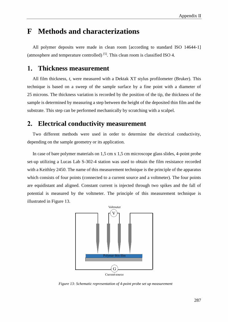
Appendix II
287
F Methods and characterizations
All polymer deposits were made in clean room [according to standard ISO 14644-1]
(atmosphere and temperature controlled) [5]. This clean room is classified ISO 4.
Thickness measurement
All film thickness, t, were measured with a Dektak XT stylus profilometer (Bruker). This
technique is based on a sweep of the sample surface by a fine point with a diameter of
25 microns. The thickness variation is recorded by the position of the tip, the thickness of the
sample is determined by measuring a step between the height of the deposited thin film and the
substrate. This step can be performed mechanically by scratching with a scalpel.
Electrical conductivity measurement
Two different methods were used in order to determine the electrical conductivity,
depending on the sample geometry or its application.
In case of bare polymer materials on 1,5 cm x 1,5 cm microscope glass slides, 4-point probe
set-up utilizing a Lucas Lab S-302-4 station was used to obtain the film resistance recorded
with a Keithley 2450. The name of this measurement technique is the principle of the apparatus
which consists of four points (connected to a current source and a voltmeter). The four points
are equidistant and aligned. Constant current is injected through two spikes and the fall of
potential is measured by the voltmeter. The principle of this measurement technique is
illustrated in Figure 13.
Figure 13: Schematic representation of 4-point probe set up measurement

Appendix II
288
If the thickness of the thin film, t, is negligible to its other dimensions, which is the case of
thin layers, then the following expression (Equation 1) of the surface resistance 𝑅 can be used:
𝑅 = 𝐾 𝑉
𝐼 (1)
𝑅 is expressed in Ω/, I is the injected current (A), V is the measured voltage (V), and K is
a geometrical factor depending on probe positioning. In thin film, 𝐾 = 𝜋/ln (2) = 4.532 [6].
Electrical conductivity σ is calculated with the following Equation 2:
𝜎 = 1
𝑅 . 𝑡 (2)
While a different method was used to obtain electrical conductivity of n-type material and
hybrid polymer/silicon devices. 2-probe set-up utilizing two gold-coated tungsten probes was
used to obtain the film resistance recorded with a Keithley 2450. Thus, by knowing the
resistance of the film R and its geometry (length L, width w, and thickness t), the electrical
conductivity could be determined (Equation 3):
𝜎 = 1
𝑅 .
𝐿
𝑤 𝑡 (3)
Unfortunately, this technique does not neglect the contact resistance generated between the
electrodes and the probes [7]. The measured total resistance consists of several components:
𝑅𝑇 = 2𝑅𝑒𝑙𝑒𝑐𝑡𝑟𝑜𝑑𝑒 + 2𝑅𝑐 + 𝑅𝑚𝑎𝑡𝑒𝑟𝑖𝑎𝑙 (4)
where R(electrode) is the resistance due to the contact metal, RC is associated with the
metal/semiconductor interface, and R(material) is the usual resistance. The resistance of a single

Appendix II
289
contact would be R(electrode) + RC. However, in most situations, the resistivity of the metal in
the contact is so low that RC >> R(electrode), and so R(electrode) can be ignored.
The material resistance is:
𝑅𝑚𝑎𝑡𝑒𝑟𝑖𝑎𝑙 = 𝑅𝑆
𝐿
𝑤 (5)
𝑅𝑇 =
𝑅𝑆
𝑤𝐿′ + 2𝑅𝑐
(6)
These results suggest a method for measuring the contact resistance. If resistors of several
different lengths are constructed (Figure 14), keeping all other details the same, the total
resistances of each can measured and plotted.
Figure 14: Schematic representation of device build to extract contact resistance
In the limit of a zero-length resistor, the residual resistance would be just twice the contact
resistance. 2RC can be found from the graph by extrapolating back to L = 0 (Figure 15).
Figure 15: Plot of the resistance as function of the distance between two electrodes.
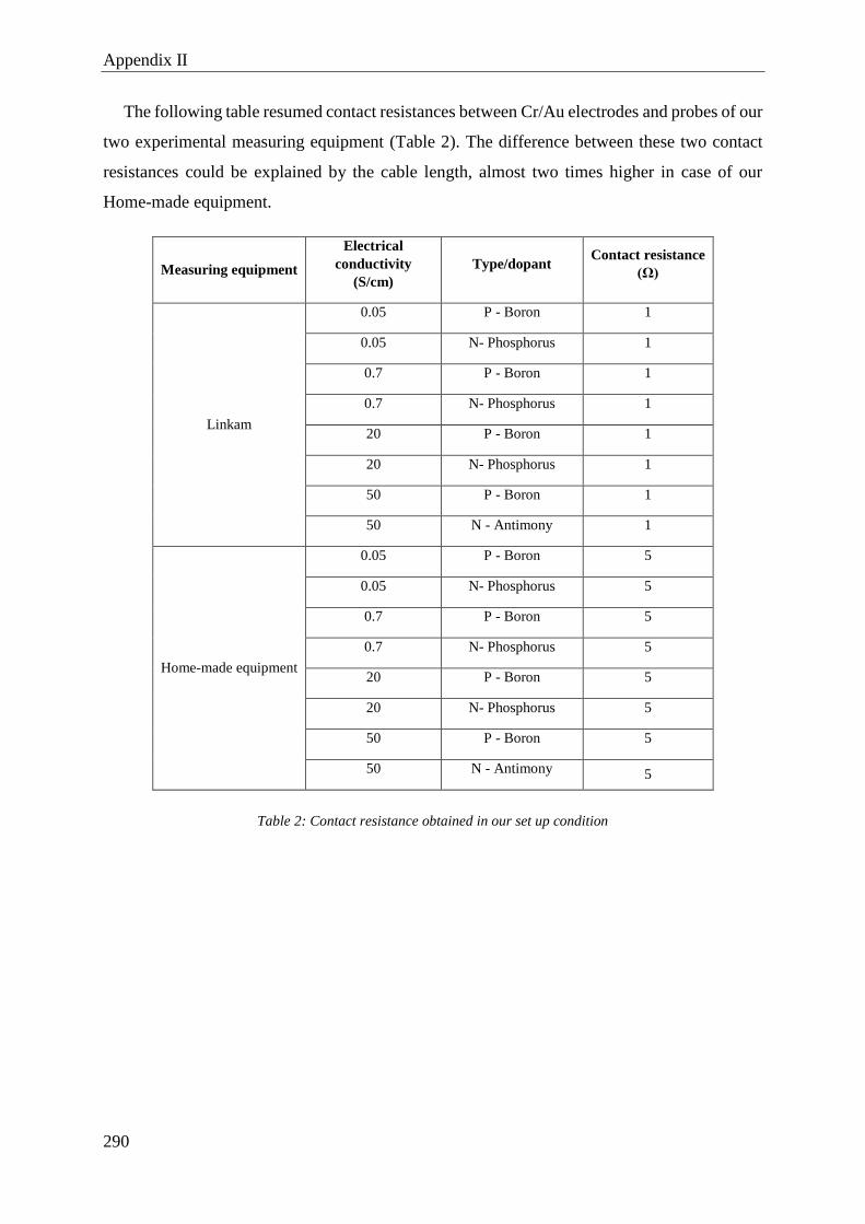
Appendix II
290
The following table resumed contact resistances between Cr/Au electrodes and probes of our
two experimental measuring equipment (Table 2). The difference between these two contact
resistances could be explained by the cable length, almost two times higher in case of our
Home-made equipment.
Measuring equipment
Electrical
conductivity
(S/cm)
Type/dopant Contact resistance
(Ω)
Linkam
0.05 P - Boron 1
0.05 N- Phosphorus 1
0.7 P - Boron 1
0.7 N- Phosphorus 1
20 P - Boron 1
20 N- Phosphorus 1
50 P - Boron 1
50 N - Antimony 1
Home-made equipment
0.05 P - Boron 5
0.05 N- Phosphorus 5
0.7 P - Boron 5
0.7 N- Phosphorus 5
20 P - Boron 5
20 N- Phosphorus 5
50 P - Boron 5
50 N - Antimony 5
Table 2: Contact resistance obtained in our set up condition

Appendix II
291
Seebeck coefficient measurement
The Seebeck coefficient was measured in thi n film geometry with two different setup
depending on the main charge carrier nature of the organic material, holes (p-type) or electrons
(n-type).
In case of p-type organic materials, the setup presented in F igure 16 was used (Home-made
set up made with Linkam Faraday cage). Two tungsten-pins coated with gold measured the
voltage, V, via a Keithley 2450, while the temperature, T, was controlled by two monitors
imposing a voltage to two Peltier plates presented Figure 16c. This is possible to close the setup
to minimize all outside disturbances. Substrates were coated with two 100 nm Cr/Au electrodes
to ensure proper electrical contact.
Figure 16: Picture of the home-made set up for Seebeck coefficient measurement of p-type material (air stable
material).
(a) (b)
(c)
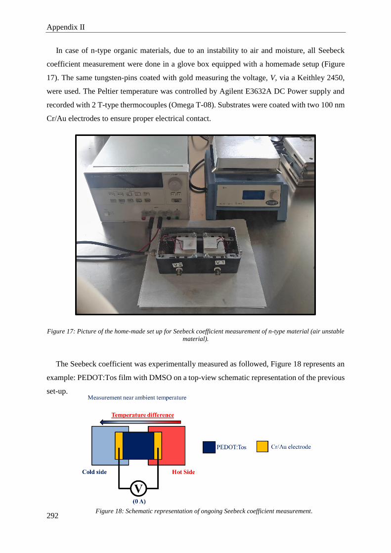
Appendix II
292
In case of n-type organic materials, due to an instability to air and moisture, all Seebeck
coefficient measurement were done in a glove box equipped with a homemade setup (Figure
17). The same tungsten-pins coated with gold measuring the voltage, V, via a Keithley 2450,
were used. The Peltier temperature was controlled by Agilent E3632A DC Power supply and
recorded with 2 T-type thermocouples (Omega T-08). Substrates were coated with two 100 nm
Cr/Au electrodes to ensure proper electrical contact.
Figure 17: Picture of the home-made set up for Seebeck coefficient measurement of n-type material (air unstable
material).
The Seebeck coefficient was experimentally measured as followed, Figure 18 represents an
example: PEDOT:Tos film with DMSO on a top-view schematic representation of the previous
set-up.
Figure 18: Schematic representation of ongoing Seebeck coefficient measurement.
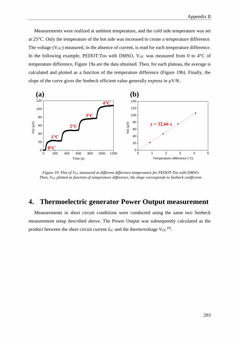
Appendix II
293
Measurements were realized at ambient temperature, and the cold side temperature was set
at 25°C. Only the temperature of the hot side was increased to create a temperature difference.
The voltage (VOC) measured, in the absence of current, is read for each temperature difference.
In the following example, PEDOT:Tos with DMSO, VOC was measured from 0 to 4°C of
temperature difference, Figure 19a are the data obtained. Then, for each plateau, the average is
calculated and plotted as a function of the temperature difference (Figure 19b). Finally, the
slope of the curve gives the Seebeck efficient value generally express in µV/K.
Thermoelectric generator Power Output measurement
Measurements in short circuit conditions were conducted using the same two Seebeck
measurement setup described above. The Power Output was subsequently calculated as the
product between the short circuit current ISC and the thermovoltage VOC [8].
(a)
0 200 400 600 800 1000 12000
20
40
60
80
100
120
Vo
c (
µV
)
Time (s)
0°C
1°C
2°C
3°C
4°C
0 1 2 3 4 50
20
40
60
80
100
120
140
Vo
c (
µV
)
Temperature difference (°C)
y = 32,66 x
Figure 19: Plot of VOC measured at different difference temperature for PEDOT:Tos with DMSO.
Then, VOC plotted as function of temperature difference, the slope corresponds to Seebeck coefficient.
(b)

Appendix II
294
Thermal imaging
Thermal images taken to verify the presence of a possible Tomson effect were recorded
using a FLIR TG165 infrared thermal imaging camera (Figure 20).
Figure 20: Commercial picture of FLIR TG165 infrared thermal imaging camera
Grazing Incidence Wide Angle X-ray Scattering
(GIWAXS)
The internal structure of the PEDOT:Tos thin films was probed using Grazing Incidence
Wide Angle X-ray Scattering (GIWAXS). GIWAXS measurements were performed on the
Dutch-Belgian Beamline (DUBBLE CRG), station BM26B, at the European Synchrotron
Radiation Facility (ESRF), Grenoble, France [9]. The energy of the X-rays was 12 keV, the
sample-to-detector distance and the angle of incidence, αi, were set at 11 cm and 0.16°,
respectively. The diffracted intensity was recorded by a Frelon CCD camera and was
normalized by the incident photon flux and the acquisition time (30 s). Flat field, polarization,
solid angle and efficiency corrections were subsequently applied to the 2D GIWAXS images
[10]. The scattering vector q was defined with respect to the center of the incident beam and has
a magnitude of q = (4π/λ)sin(θ), where 2θ is the scattering angle and λ is the wavelength of the
X-ray beam. Herein we opted to present the wedge-shape corrected images where qr and qz are
the in-plane and near out-of-plane scattering vectors, respectively. The scattering vectors are
defined as follows: qx = (2π/λ)(cos(2θf)cos(αf)-cos(αi)), qy = (2π/λ)(sin(2θf)cos(αf)), qz =

Appendix II
295
(2π/λ)(sin(αf)+sin(αi)), qr² = qx² + qy², where αf is the exit angle in the vertical direction and 2θf
is the in-plane scattering angle, in agreement with standard GIWAXS notation [11].
X-ray Photoelectron Spectroscopy (XPS) and
Ultraviolet Photoelectron Spectroscopy (UPS)
X-Ray Photoelectrons Spectroscopy (XPS) and Ultraviolet Photoelectrons Spectroscopy
(UPS) were performed on the platform ELORPrintTec. Electron spectroscopy measurements
were carried out in an ultrahigh vacuum chamber SPECS (10-9 mbar). All the samples were
stored in gloves box before being analyzed by photoelectron spectroscopy in order to keep the
surface in the same state than after deposition.
For UPS, a UHV surface analysis system equipped with a Scienta-200 hemispherical analyzer
was used. All measurements were performed using He(I) with a low intensity UV light (21.22
eV).
In case of XPS analysiss, a monochromatized Al Kα X-ray source with an energy of 1486.6
eV allowed to obtain all results.

Appendix II
296
Oxidation level calculation
The oxidation level is relative to the amount of tosylate counter-anion per unit of thiophene
unit. So, the ratio of the area for reacted tosylates contribution on the area for all thiophenes
unit contribution gives the oxidation level [12].
162 164 166 168 170
Co
un
ts (
arb
. u
nits)
Binding energy (eV)
Figure 21: (a) S(2p) XPS spectra for PEDOT:Tos film. (b) Schematic PEDOT:Tos forming reaction from EDOT
monomer and Fe(Tos)3. Each color represents a different sulfur: Doublet thiophene unit cation (red and
orange), doublet thiophene unit (green and blue), tosylate counterion (purple and rose) and tosylate counterion
charged (cyan and brown).
𝑂𝑥𝑖𝑎𝑡𝑖𝑜𝑛 𝑙𝑒𝑣𝑒𝑙 = 𝐴𝑟𝑒𝑎𝑟𝑒𝑎𝑐𝑡𝑒𝑑 𝑇𝑜𝑠𝑦𝑙𝑎𝑡𝑒
𝐴𝑟𝑒𝑎𝑇ℎ𝑖𝑜𝑝ℎ𝑒𝑛𝑒
(a)
(b)

Appendix II
297
Atomic Force Microscopy (AFM)
Atomic force microscopy (AFM Dimension FastScan, Bruker) was used in tapping mode to
characterize the surface morphology of the samples. Silicon cantilevers (Fastscan-A) with a
typical tip radius of ≈5 nm, a spring constant of 18 N.m−1 and a cantilever resonance frequency
of about 1.4 MHz were used.
Scattering Electron Microscopy (SEM)
SEM images were obtained with a Scanning electron microscope – JEOL 7800 – E prime.
LED detector with an acceleration of 2 kV permitted to obtain high resolution images. Analysis
were done in ElorPrinTec facilities (University of Bordeaux, Building B8). The infrastructure
consists of an 850m² cleanroom which houses 5 equipment clusters. The cleanroom is entirely
qualified to ISO 6 conditions and temperature and humidity are strictly controlled. This
guarantees optimal and very constant working conditions.
Transmission Electron Microscopy (TEM)
TEM images were obtained on Formvar grids with a Transmission Electron Microscope
(H7650, HITACHI (accelerate voltage 120 kV)), using high contrast mode. Analysis were done
in the Bordeaux Imaging Center (University of Bordeaux, Electronic Unit, Centre Génomique
Fonctionnelle Bordeaux).
UV-Visible measurement (UV-Vis)
Absorption spectra were measured using a Shimadzu spectrophotometer UV-3600.
Nuclear Magnetic Resonance (NMR)
NMR spectra were recorded on a Bruker Avance III 400 spectrometer at 400 MHz for 1H
nucleus.
Size Exclusion Chromatography (SEC)
Size exclusion chromatography (SEC) was performed in TCB at 150°C with a flow rate of
1 mL.min-1 using Agilent PL gel MIXED C column (pore size 5 µm) and an Agilent PL gel
guard-column. The elution times were converted into molecular weights using a calibration
curve based on low dispersity polystyrene standards.
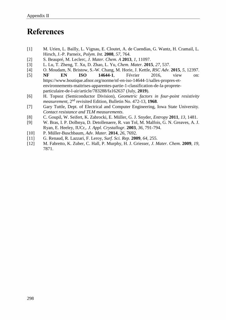
Appendix II
298
References
[1] M. Urien, L. Bailly, L. Vignau, E. Cloutet, A. de Cuendias, G. Wantz, H. Cramail, L.
Hirsch, J.-P. Parneix, Polym. Int. 2008, 57, 764.
[2] S. Beaupré, M. Leclerc, J. Mater. Chem. A 2013, 1, 11097.
[3] L. Lu, T. Zheng, T. Xu, D. Zhao, L. Yu, Chem. Mater. 2015, 27, 537.
[4] O. Moudam, N. Bristow, S.-W. Chang, M. Horie, J. Kettle, RSC Adv. 2015, 5, 12397.
[5] NF EN ISO 14644-1, Février 2016, view on:
https://www.boutique.afnor.org/norme/nf-en-iso-14644-1/salles-propres-et-
environnements-maitrises-apparentes-partie-1-classification-de-la-proprete-
particulaire-de-l-air/article/783288/fa162637 (July, 2019).
[6] H. Topsoz (Semiconductor Division), Geometric factors in four-point resistivity
measurement, 2nd revisited Edition, Bulletin No. 472-13, 1968.
[7] Gary Tuttle, Dept. of Electrical and Computer Engineering, Iowa State University.
Contact resistance and TLM measurements.
[8] C. Goupil, W. Seifert, K. Zabrocki, E. Müller, G. J. Snyder, Entropy 2011, 13, 1481.
[9] W. Bras, I. P. Dolbnya, D. Detollenaere, R. van Tol, M. Malfois, G. N. Greaves, A. J.
Ryan, E. Heeley, IUCr,. J. Appl. Crystallogr. 2003, 36, 791-794.
[10] P. Müller‐Buschbaum, Adv. Mater. 2014, 26, 7692.
[11] G. Renaud, R. Lazzari, F. Leroy, Surf. Sci. Rep. 2009, 64, 255.
[12] M. Fabretto, K. Zuber, C. Hall, P. Murphy, H. J. Griesser, J. Mater. Chem. 2009, 19,
7871.

299

300
Appendix III
301
Appendix III:
Silicon nanowires as a filler

Appendix III
302
A Preface
Recently, improvements on the figure of merit ZT, have been achieved in inorganics
thermoelectric materials (e.g., superlattices, nano-inclusions, nano-composites, etc.) [1,2], in
particular, by phonon scattering to preferentially reduce the thermal conductivity without the
loss of power factor, R. [2] and by energy filtering to independently promote the Seebeck
coefficient without greatly suppressing electrical conductivity [3]. However, these complex
inorganic materials are generally prepared by either the ball-milling, melt-spinning method or
molecular beam epitaxy, which involves high-temperature, long-term and high-cost fabrication
processes [4].
So, several teams work to develop a facile and l ow-cost fabrication process for inorganic
TE materials, including wet-chemical synthesis [5], solution-processable nanocomposites [4],
and polymer TE materials [6]. The strategy of introducing inorganic materials interfaces to
scatter phonons or filter low-energy carriers seems to also work well in polymer TE materials.
In this work, a rationally engineering of the organic–inorganic semiconductor interfaces of
polymer nanocomposites were conducted to improve the Seebeck coefficient and power factor
via the energy-filtering effect [7]. Herein, an organic–inorganic interface was created by mixing
inorganic nanoparticles into a polymer matrix through a solution-processable route. Based on
previous results described in this manuscript, PEDOT:Tos treated with DMSO and pyridine
was chosen as organics material. This polymer obtained the best thermoelectric performances
among tested organic materials. Then, as inorganic nanoparticle material, silicon nanowires
were chosen due to their role in the enhancement of TE properties for hybrid polymer/silicon
devices. A home-made procedure developed in the laboratory, allowed to recover a suspension
of SiNWs in an organic solvent. Finally, a solution-processable fabrication of nanocomposites
was also developed.
B Silicon nanowires suspension
First, silicon nanowires were prepared by following the procedure in Appendix II. Then,
the silicon treated substrate was placed inside a small container, and immerged with 1 mL of
ethanol. This container (closed) was placed 1 hour in an ultrasonic bath at room temperature.
The highest ultrasounds intensity possible was set. After one hour, the ethanol turns to a trouble
brown-grey solution, and the silicon substrate shows some area with the mirror effect of the

Appendix III
303
bare silicon. By repeating this process, one silicon substrate allows to obtain 0.2 mg of “silicon
nanoparticles”. In order to confirm the extraction of SiNWs from the substrate, SEM was
performed on silicon treated substrate, results are presented in Figure 1.
Figure 1b and 1c represent the side view of SiNWs after one and three cycles inside the
ultrasonic bath, respectively. This is clearly visible that some silicon nanowires parts were cut-
off their basis.
Figure 1: SEM picture of (a) bare silicon nanowires, (b) SiNWs after 1 hour in ultrasonic bath and (c) SiNWs
after 3 times 1 hour in ultrasonic bath.
In parallel, the “silicon nanoparticles” in the ethanol solution were analyzed by TEM and
AFM (Figure 2). Both techniques confirmed the presence of silicon nanowires. Figure 2a shows
particles heterogeneity, they aren’t all silicon nanowires and their size differs. Two
magnification confirmed this result (Figure 2b and 2c). Finally, the silicon nanowires have been
dried under Nitrogen flux.
10 µm
10 µm 10 µm
(a)
(b) (c)

Appendix III
304
C PEDOT:Tos/SiNWs film composite
The inorganic/polymer composite thin film were made following the next procedure.
Polymerization directly takes place during the film process. The SiNWs were introduced inside
the oxidative formulation DMSO + pyridine. Unfortunately, in view of the difficulty to recover
high quantities of silicon nanowires, only 0.1 wt% (3 mg) were mixed with this oxidative
formulation. So, 9,9 µL of EDOT were added to 300 µL of the oxidative formulation with
0.1 wt% of SiNWs. The mixture was stirred 30 s before processing. On cleaned / treated
substrate (see Substrate cleaning / treating procedure), oxidant and SiNWs/EDOT mixture, was
spin-coated at 1500 rpm for 30 s with a ramp of 800 rpm/s². The resulted thin films were
annealed on a hot plate (100°C) in ambient conditions for 15 min. Afterwards, the film was
sequentially washed with two 1-butanol bath and one ethanol bath during 5 min per bath. The
resulting thin films was visually rougher.
(a) (b)
(c) (d)
Figure 2: TEM and AFM images of SiNWs after ultrasonic bath.

Appendix III
305
The effect of silicon nanowires on PEDOT:Tos thermoelectric properties was investigated.
Electrical conductivity σ, Seebeck coefficient S and power factor PF are presented Table 1. The
small amount of SiNWs (0.1 wt%) have a significate impact on Seebeck coefficient, which
increased at 50 µV/K. However, the electrical conductivity decreased almost by a factor of two,
1240 to 814 S/cm. The power factor, S²σ, reached a value of 203 µW/m.K² for the film with
0.1 wt% of SiNWs.
Name S (µV/K) σ (S/cm) PF (µW/m.K²)
PEDOT:Tos DMSO+pyridine 44 ± 3 1240 ± 12 240.1
PEDOT:Tos DMSO+pyridine
+ 0.1 wt% SiNWs 50 814 203
Table 1: Thermoelectric properties of the corresponding PEDOT:Tos films with and without SiNWs as filler
This decreasing electrical conductivity could be due to a morphological change of the semi-
crystalline PEDOT:Tos thin film. SEM analysis was performed in order to investigate this
phenomenon (Figure 3). No whole nanofiber is visible; only inorganic aggregates are present
(pointed by white arrows). The presence of these pieces of fibers may be due to the experimental
conditions, for example, agitation prior to deposition. In addition, the film is clearly
inhomogeneous, this may explain the drop in electrical conductivity. As has been shown in
Chapter 2, the film structure plays a fundamental role in the transport of charges, and hence the
electrical conductivity.
Figure 3: Top view SEM image of PEDOT:Tos with SiNWs.
White arrows point silicon aggregates.
100 µm

Appendix III
306
D Conclusion
In this study, SiNWs were recovered using an ultrasonic bath. Subsequently, silicon
nanoparticles were embedded in a film of PEDOT: Tos treated with DMSO and pyridine.
Despite an increase in the Seebeck coefficient, the power factor of this composite film was
lower than the polymer film alone. The reason could be a modification in the morphology of
the film (confirmed by SEM). It would be interesting to study this approach in greater depth.
For example, by controlling more finely the incorporation of these SiNWs in the film, so as not
to harm the crystallinity. Finally, more of these particles should be added to see their effect. A
bell-like shape could be obtained, with a maximum greater than the TE performance of the
polymer alone, for higher amounts.
Appendix III
307
References
[1] F. Wu, H. Song, F. Gao, W. Shi, J. Jia, X. Hu, J. Electron. Mater. 2013, 42, 1140.
[2] R. Venkatasubramanian, E. Siivola, T. Colpitts, B. O’Quinn, Nature 2001, 413, 597.
[3] K. Koumoto, T. Mori, Thermoelectric Nanomaterials: Materials Design and
Applications; Springer Science & Business Media, 2013.
[4] D.-K. Ko, Y. Kang, C. B. Murray, Nano Lett. 2011, 11, 2841.
[5] J. S. Son, M. K. Choi, M.-K. Han, K. Park, J.-Y. Kim, S. J. Lim, M. Oh, Y. Kuk, C.
Park, S.-J. Kim, T. Hyeon, Nano Lett. 2012, 12, 640.
[6] C. Yu, Y. S. Kim, D. Kim, J. C. Grunlan, Nano Lett. 2008, 8, 4428.
[7] K. C. See, J. P. Feser, C. E. Chen, A. Majumdar, J. J. Urban, R. A. Segalman, Nano
Lett. 2010, 10, 4664.

308

Titre : Matériaux polymères/silicium hybrides pour des applications
thermoélectriques
Résumé :
De nos jours, l’Homme cherche principalement à gérer les énergies et leurs utilisations dans une
perspective de développement durable. Parmi les différentes énergies renouvelables, la thermoélectricité
semble être une solution de choix pour la conversion de la chaleur en électricité, améliorant ainsi les
rendements thermiques. Les matériaux thermoélectriques pour les applications à température ambiante
sont dominés par les matériaux à base de tellurure de bismuth (Bi2Te3) qui offrent la meilleure efficacité.
Cependant, leur coût et leur toxicité empêchent leur développement à grande échelle. Ces dernières
années, bien que possédant des caractéristiques thermoélectriques plus faibles que le Bi2Te3, les
matériaux polymères ont été envisagés comme une alternative prometteuse. L'objectif de cette thèse
était donc de développer des matériaux polymères et hybrides (i.e. en combinaison avec des
inorganiques) thermoélectriques performants dans le but de réaliser un générateur thermoélectrique
(GTE) efficace. Nous avons choisi d'étudier le PEDOT, le P3HT et le PCDTBT comme polymères, et
le Silicium comme matériau inorganique. Plusieurs voies d'optimisation ont ainsi été explorées, soit en
ajustant le niveau de dopage, soit en adaptant la surface des matériaux inorganiques et leurs interfaces.
Des GTEs ont été développés pour des applications proches de la température ambiante. Le couplage
entre un matériau polymère et le silicium a notamment permis d’obtenir une amélioration significative
des performances et d’atteindre une valeur record par rapport à l'état de l'art du domaine.
Mots clés : Thermoélectricité, Polymère, Silicium, Générateur
Title: Hybrid polymer/silicon materials for thermoelectric applications
Abstract:
Nowadays, human beings seek mainly to manage energy and their uses toward sustainable development.
Among the various renewable energies, thermoelectricity is the solution for the conversion of heat losses
into electricity, and therefore the improvement of thermal efficiency. Thermoelectric materials for room-
temperature applications are dominated by bismuth telluride (Bi2Te3) based materials offering higher
efficiencies. Nevertheless, their cost and toxicity prevent large-scale applications. In recent years,
polymer materials have been considered as alternatives for Bi2Te3, although their thermoelectric
properties are significantly lower. The aim of this thesis was therefore to develop an efficient
thermoelectric polymer, in combination with an inorganic material in order to obtain an efficient
thermoelectric generator. PEDOT, P3HT and PCDTBT were chosen as p-type polymers and silicon
substrates as semi-conducting inorganic materials due to their high importance and performance in their
respective fields. Several optimization routes have been investigated, either by fine-tuning the doping
level parameters or by tailoring the surface of the inorganic materials. Hybrid thermoelectric generators
(TEGs) were developed for near room temperature application. The coupling with polymer material
achieved to obtain an enhancement of device performances resulting in record value.
Keywords: Thermoelectricity, Polymers, Silicon, Generator
Laboratoire de Chimie des Polymères Organiques UMR 5629, 16 Avenue Pey-Berland, Pessac Cedex, F-33607, France.