
Structure, hardness and thermal stability of nanolayered TiN/CrN multilayer coatings

Optimization of multilayer porous silicon antireflection coatings for siliconsolar cells
J. H. Selj,1,2,a� A. Thøgersen,1 S. E. Foss,1 and E. S. Marstein1
1Department of Solar Energy, Institute for Energy Technology, Instituttveien 18, 2007 Kjeller, Norway2Department of Physics, University of Oslo, Pb 1048 Blindern, 0316 Oslo, Norway
�Received 6 November 2009; accepted 1 February 2010; published online 15 April 2010�
Efficient antireflection coatings �ARC� improve the light collection and thereby increase the currentoutput of solar cells. In this work, multilayered refractive index stacks optimized for antireflection,in bare air and within modules, are modeled. The relation between porous silicon �PS� etchingparameters and PS structure is carefully investigated using spectroscopic ellipsometry, gravimetry,x-ray photoelectron spectroscopy, and scanning electron microscopy. The close relation betweenporosity and refractive index, modeled using the Bruggeman effective medium approximation,allows PS multilayers to be tailored to fabricate the optimized ARCs. Limits imposed by efficientapplication in photovoltaics, such as thickness restrictions and the angular distribution of incidentlight, are examined and accounted for. Low reflectance multilayer ARCs are fabricated withintegrated reflectances of �3% in air and 1.4% under glass in the wavelength range 400–1100 nm.© 2010 American Institute of Physics. �doi:10.1063/1.3353843�
I. INTRODUCTION
One cardinal goal for photovoltaic power production isto reach grid parity. Two routes exist to reach this goal;higher efficiency and lower production costs. Porous silicon�PS� has several possible applications in photovoltaics andholds potential to contribute to the desired development.1,2
This paper will focus on using PS for antireflection purposesin solar cells. The most commonly used antireflection coat-ing �ARC� for silicon solar cells is silicon nitride,3,4 having areported integrated reflection in the order of 10% for monoc-rystalline wafers over the spectral range of interest.5,6 Thereflection will, however, be further reduced with standardtexturing. For a single layer ARC, the reflection is minimizedat one single wavelength given by �min=4nd, where n is therefractive index and d is the thickness of the layer.
Excellent broadband ARCs with reflectance less than 3%are obtainable today with a multilayered structure, such asMgF2 /Al2O3 /ZnS, where each layer is seperately deposited.7
However, multiple depositions increase the cost and in addi-tion, magnesium fluoride, and zinc sulfide are soft and easilydamaged.8 PS offers a simpler one-step production of multi-layered stacks. Using electrochemical etching, the refractiveindex, which is closely related to the porosity, can be tuned.This provides fast and inexpensive manufacture of multilay-ered ARCs. Excellent broadband reflectivity has been dem-onstrated for PS.9 However, the stacks made in this case aretoo thick �1 �m� for efficient photovoltaic application. Sucha large thickness would cause degradation of the electricalcharacteristics of the solar cell as the typical commercialjunction depths are on the order of 350 nm. Deeper diffu-sions are possible but expensive. In addition, PS shows sig-nificant absorption and, therefore, in an optimal coating, re-flection must be weighted against absorption. It has been
demonstrated that good coatings may be achieved alsowithin these limits but an optimal coating has not beenobtained.10
This paper presents an optimization of multilayeredARCs for photovoltaic application. A systematic study is car-ried out to achieve an accurate determination of the effect ofetching parameter variations in the PS structure. In particu-lar, it is important to have a broad porosity span to access themaximum refractive index range. It has been discussed thatthe porosity span accessible by current density variations inthin films is broader than that of thick films because surfaceand interface roughness increase the porosity span in bothdirections.10 However, to our knowledge, systematic experi-mental studies of the obtainable porosity span for thin filmsat different concentrations of hydroflouric acid �HF� have notbeen reported. This will, therefore, be the first step toward anoptimized PS ARC.
The optimal ARC is then modeled with constrictionson the available porosity-range and with respect to applica-tion in photovoltaics. The optimization is carried out bothfor operation in air ambient and in encapsulated modules.After formation of the coating, spectral reflectance is mea-sured in the wavelength range 400–1100 nm. An integratedreflection of �3% is obtained for samples optimized withoutglass. Within a module, a reflection of 5.6%, including re-flections from the air-glass interface, is obtained. This com-pares favorably with todays commercial single and doublelayer coatings �SiNx,
3 MgF2 /ZnS,7 SiO2 /TiO2,11 andMgF2 /CeO2.12
II. EXPERIMENTAL
A double cell electrochemical etching system, PSB Plus4 from advanced micromaching tools �AMMT�, was used toproduce the PS layers. The wafers used were boron doped,300–550 �m thick, one side polished, monocrystallinesilicon with a �100� orientation. The nominal resistivitiesa�Electronic mail: [email protected].
JOURNAL OF APPLIED PHYSICS 107, 074904 �2010�
0021-8979/2010/107�7�/074904/10/$30.00 © 2010 American Institute of Physics107, 074904-1

were 0.01–0.05 � cm. However, four point probe measure-ments were used to determine the resistivity range to0.012–0.018 � cm. The high doping densities are necessaryto ease the current flow by reducing the potential barrier forholes between electrolyte and wafer. Alternatively, surfacedoping of standard solar cell wafers of 1–3 � cm could beused for the same purpose. The wafers were dipped in 5%HF to remove native oxide. A mix of 49 wt % HF and eth-anol �C2H5OH� constituted the electrolyte. HF concentra-tions were varied from 10% to 20% �volume ratio� to find theoptimal porosity span. The special purpose potensiostat, PS2
from AMMT, allowed programming of current density pro-files with a time resolution of 50 ms. After etching, thesamples were rinsed in ethanol to avoid cracking due to cap-illary forces during drying. For samples optimized for use inmodules, microscope glass of 1 mm thickness was laminatedto the samples, using ethylene vinyl acetate �EVA� as encap-sulant.
Ellipsometry measurements were carried out using aWoollam variable angle spectroscopic ellipsometer�WVASE� in the wavelength range 300–1100 nm. To de-crease the impact of sample inhomogeneities and depolariza-tion on the measured data, focus probes with a spot diameterof 0.2 mm were applied. On the single layers, variations inthe PS layer are evident by visual inspection. This may bedue to small variations in resistivity or current density overthe sample. For the graded layers no significant inhomoge-nety can be seen by visual inspection. Gravimetry was usedas a control technique to check a selection of the porositiesobtained from ellipsometric measurements. The porositiesobtained from ellipsometry are, in all cases, confirmed bygravimetry to within 3% absolute. In gravimetry the wafersare weighted before �m0� and after �m1� PS formation. Thewafer is then etched in 2% KOH to effectively remove thePS layer and subsequently weighted again �m2�. Porosity, P,and thickness, t, of the PS layer, is then calculated from
P =m0 − m1
At�,
and
t =m0 − m2
A�,
where �=2.33 g /cm2 is the density of silicon and A isthe area where PS is formed. For the samples where scanningelectron microscopy �SEM� and transmission electron mi-croscopy �TEM� images are taken, the thickness displayedby these methods are in correspondence with results fromellipsometry and gravimetry. Thickness and layer structurewere also investigated using SEM and TEM. Cross-sectionalTEM samples were prepared by ion-milling using a Gatanprecision ion polishing system with 5 kV gun voltage. Thesamples were analyzed by high resolution TEM in a 200 keVJEOL 2010F microscope. X-ray photoelectron spectroscopy�XPS� was used to assess the amount of oxide in thesamples. XPS was performed in a KRATOS AXISULTRADLD using monochromated Al K� radiation �h�=1486.6 eV� on plane-view samples at zero angle of emis-
sion �vertical emission�. The x-ray source was operated at 10mA and 15 kV. The spectra were peak fitted using CasaXPS13 after subtraction of a Shirley type background. Fi-nally, reflectance was measured using a spectral responseunit in the wavelength range 400–1100 nm.
III. FABRICATION AND STRUCTURE
A. PS fabrication
To access a large range of refractive indices in one singleetch, the optimal etching parameters must make a broad spanin porosities available by varying only the current density.Three different HF concentrations were tested for the pur-pose of obtaining the widest porosity range, 10%, 15%, and20%. As expected, in all cases, the porosity increased withcurrent density up until the limit of electropolishing.14 TableI shows the porosity span available at the various electrolytecompositions. The lowest available porosity is assessed usinga current density of 1 mA /cm2, the highest porosity is as-sessed using the highest current density which does not giveelectropolishing. An electrolyte consisting of 20% HF gavethe broadest porosity range and was, therefore, used in allfurther experiments.
Although much is published on the properties of PS andhow these vary with current density, resistivity, electrolytecomposition, etc,15–18 the PS layer is so sensitive to etchingparameters, wafer-properties, and environment that it is nec-essary to undertake careful investigations of the relations be-tween these parameters for our specific setup. Especially therelation between current density and porosity and betweencurrent density and etch rate must be known in great detail toenable the production of the best performance modeled layerat a later stage. Figure 1 shows porosities and etching rate
TABLE I. Porosity limits.
Current density J�mA /cm2� 10% HF 15% HF 20% HF
1 ¯ 38 265 76 49 40Max�18/80/250� 90 80 76
0 50 100 150 2000
10
20
30
40
50
60
70
80
90
100
Porosity(%)
Current Density (mA/cm2)
PorosityEtchrate
0 50 100 150 2000
10
20
30
40
50
60
70
80
90
100
EtchRate(µm/s)
FIG. 1. �Color online� Current density vs porosity and etch rate in a 20% HFsolution at room temperature, as determined from ellipsometry andgravimetry.
074904-2 Selj et al. J. Appl. Phys. 107, 074904 �2010�

versus current density during formation, as determined byellipsometry, gravimetry, and SEM. The curve suggests anonlinear relationship between current density and porosity,with the steepest gradient at low current densities. Here, theporosity displays a particularly large increase, from 26% at1 mA /cm2 to 42% at 14 mA /cm2. Although a sharp in-crease at low current densities is not unexpected based onresults published by Ref. 19 for similar sets of process pa-rameters, we have increased the sampling frequency and per-formed ten PS etches within this current density range. Alletched samples comply with the low porosity trend.
In this work, heavily doped silicon wafers with a con-stant doping density are used. In a typical solar cell emitter,the doping density has a certain doping gradient normal tothe surface which can affect the porosity profile. Two ap-proaches can be used to address this issue. In one approach,varying resistivities can be compensated for in the final cur-rent density profiles used for etching the ARCs. Alterna-tively, the doping profile can be tailored to give a relativelyflat gradient in the resistivity.20
TEM images show that the distance between the siliconwalls varies between 7–30 nm, indicating that a mesoporousmaterial is formed. The interface between the PS layer andthe silicon substrate is rather wavy. This is promising withrespect to the light spreading properties of the film. TEMimages also reveal that the pores are columnar with signifi-cant branching �Fig. 2�. The pores point predominantly to thesurface, while the branches, or secondary pores, are not re-stricted to the �100� plane. For �100� wafers, a preferentialgrowth perpendicular to the surface and towards the sourceof holes is expected. This is due to differences in the passi-vation speed of the different crystallographic directions.21
The passivation process works fastest on the �111� surfacesand these surfaces, therefore, show a reduced probability ofbeing etched.22
B. Ellipsometric characterization of PS
It is well known that the optical properties of PS can bemodeled as a mix of Si and voids in an effective mediumapproximation �EMA�.23,24 In this work, the BruggemanEMA �BEMA� �Ref. 25� theory is used. It gives a good ap-proximation for mesoporous silicon, especially when porosi-ties are not too high.26–28 Amorphous silicon was tested as aconstituent of the EMA but with poorer results than crystal-
line silicon �c-Si�. This indicates that the PS layers are crys-talline, as expected. This was confirmed by selected areadiffraction �SAD� images of the samples, see Fig. 3.
Ellipsometric measurements are used here primarily toobtain the thickness and porosities of the layers. Knowingthe thickness of the films, etch rates can easily be calculated.Ellipsometry is based on measuring changes in polarizationdue to interaction with the sample surface. This change ismeasured as the ratio of the Fresnel coefficients for parallel�rp� and perpendicularly �rs� polarized light. The ratio is usu-ally given in terms of the ellipsometric parameters � and �
rp/rs = tan � exp i� .
Therefore, physical parameters, i.e., optical and microstruc-tural properties, are not immediately given but must be de-duced from the measured data by modeling. Analysis of theoptical data is performed using the WVASE software pack-age, WVASE32, which is designed to fit a generated model toa given set of observed data. In the modeling we make use ofthe tabulated refractive indices of silicon reported by Herz-inger et al.29
For graded layers, the modeling is approached by use ofstratified medium theory; ellipsometric data from arbitrarygraded index ARCs are reproduced by a variation in n�z�with depth.30 The best fit n�z� profile can be found by divid-ing the film into a small number of homogeneous sublayersparametrized by a thickness and complex refractive index.Alternatively, a model function can be used. In this approachthe film is again divided into homogeneous layers but thenumber of layers is so high that the optical properties areidentical to those of a continuous medium.31 In this work, theformer procedure is utilized and should be appropriate, as theARCs indeed are made using a quite limited number of step-wise variations in the current density rather than a continousvariation.
Shape anisotropy introduces optical anisotropy in thesamples, in principle requiring generalized ellipsometry anda generalized BEMA model. Such a generalized BEMA ispreviously shown to be a good approximation of birefringentPS.28,32 However, standard ellipsometry is sufficient if theoptical axis of a sample with uniaxial anisotropy is lyingperpendicular to, or parallel with, the sample surface. Aspreviously discussed, TEM images showed substantial
FIG. 2. TEM image of a PS sample, etched for 15 s at a current density of20 mA /cm2, shows columnar pores mainly pointing towards the surface.Significant branching is also evident.
FIG. 3. SAD patterns from the Si substrate to the left and the central area ofthe porous layer to the right, showing that the crystalline walls in the porousregion remain as a single crystal. Only a slight variation in orientation isseen inside the porous region. The diffuse rings in the pattern from theporous region are identical to the rings observed for the epoxy used in thesample preparation.
074904-3 Selj et al. J. Appl. Phys. 107, 074904 �2010�

branching, secondary pores which are not restricted to the�100� plane. Therefore, both generalized and standard ellip-sometry were performed. Generalized ellipsometry did notshow any sign of in-plane anisotropy and standard ellipsom-etry together with a perpendicular uniaxial model was, there-fore, adopted in the following work. The columnar shape ofthe microstructure induces distinct boundary conditions tothe electrical and magnetic field in the medium. In theuniaxial BEMA, this charge screening is modeled by thedepolarization factor, qz.
In the single layer models, qz is allowed to vary giving abest fit between 0.25 and 0.3. Given the columnar shape andsignificant branching of the pores �Fig. 2�, ellipsoids slightlyelongated along the pores are a plausible form of the depo-larization. As the best fit qz is relatively consistent in allsingle layer samples, in the more complex models it is fixedto 0.28 to reduce the number of fitting parameters. The qx
and qy components are equally split and describe the in-planesymmetry.33
TEM images reveal that even for PS layers where thecurrent density during etching has been kept constant, thepores are not uniform along the vertical direction. The fit ofthe ellipsometry models also improves by adding a smallgradient where each sublayer is modeled as a mixture of c-Siand voids. A porosity grading can account for the interfaceroughness between the substrate and the porous layer andbetween the porous layer and air.34,24 In addition, chemicaletching may contribute to a further etching of the uppermostpart of the PS layer. Numerical algorithms are used to varythe unknown parameters and minimize the difference be-tween simulated and experimental data.
In WVASE, the Levenberg–Marquardt minimizationroutine is used. The goodness of the fit is measured by themean squared error �MSE�. The models are generally wellfitted with MSEs15, except some of the thick and highlydepolarizing samples which have somewhat higher MSE.However, almost all models show some deviations from theexperimental data in the blue region �300–400 nm�. This islikely because the the wavelength approaches the nanostruc-ture size ��air=300 nm⇒�Si�70 nm� and therefore ap-proach the end of the applicability range of the static effec-tive medium theory.28
Generally, PS has a strong aging process where it oxi-dizes in air ambient and at room temperature. The presenceof SiO2 is neglected in the ellipsometric fitting for two rea-sons. First, XPS images show that the oxide content of thePS samples is relatively low, about 9% at a depth of approxi-mately 20 nm, see Fig. 4. PS made from low resistivityp-type material �0.01 � cm� has also previously been re-ported to have little oxide content.35
Second, the SiO2 has a relatively small optical contrastto void, and it is therefore difficult to separate the opticalprints of the two. It should be noted, though, that SiO2 con-sumes both pores and Si pore walls. Based on the densitiesand molecular weights of Si�dSi=2330 kg /m3, MwSi
=28.0855 g /mol� and SiO2�dSiO2=2200 kg /m3, MwSiO2
=60.0843 g /mol� it can be seen that for an oxide of thick-ness t, the fractional consumption of the silicon wall is
MwSi/dSi
MwSiO2/dSiO2
= 0.44t ,
while the remaining 0.56t is expansion into the pores. Forlarge oxide contents this could result in an overestimation ofthe porosity and a more accurate model might have to take ashell-like structure into consideration. However, such a pro-cedure would increase the number of fitting parameters andcould result in parameter correlation problems.36 For the PSsamples presented here, oxide content is low and neglectingthe SiO2 does not induce significant error. As a result, theEMA model including solely c-Si and void is a good ap-proximation.
IV. MODELING IDEAL ARCS
To determine the optimal structure of the ARC, simula-tion is performed in the WVASE32 software. In WVASE32, thebest fit structure is constructed within the frame of the gen-erated model by varying a chosen set of parameters. In thisoptimization, the generated model is a uniaxially anisotropicBruggeman approximation, i.e., the same type of model thatis used to model the ellipsometric data from the real PSlayers. We constructed a zero reflection data set which wasfed to the program instead of measured data. This zero re-flection file was then used as the fitting target. The data filewas weighted with respect to the solar spectrum �1.5 AM�and cut-off at 1100 nm, corresponding approximately to thebandgap of silicon. At 1200 nm the absorption coefficient ofsilicon has decreased by two orders of magnitude. Glass withrefractive index of 1.52 at 500 nm is used as ambient for theARC optimized for use in mudules.
Using Snell’s law it can easily be seen that a ray hittingthe glass cover at an angle of 10° to the sample surface, willbe refracted in the glass and hit the ARC at an angle of 49°to the surface. Therefore, there is no need to accommodatevery small incident angles in the modeling. The zero reflec-tion data file, therefore, incorporates relevant incident angles�50°, 60°, 70°, 80°, and 90° to the cell surface�. No differen-tiation has been made between the weighting of the fiveangles which are accounted for.
The modeling confirms the excellent antireflection prop-erties demonstrated by Uehara et al.9 The models are ideal inthe sense that they have the total refractive index range avail-able �nair−nSi� and no imposed limits on thickness. Both
FIG. 4. The XPS Si 2p spectrum of the PS sample. The spectrum was peakfitted with four peaks corresponding to Si4+�SiO2�, Si2+�SiO�, Si+�Si2O�, andSi0 �pure Si�.
074904-4 Selj et al. J. Appl. Phys. 107, 074904 �2010�
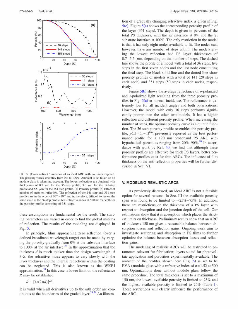
these assumptions are fundamental for the result. The start-ing parameters are varied in order to find the global minimaof reflection. The results of the modeling are displayed inFig. 5.
In principle, films approaching zero reflection �over adefined broadband wavelength range� can be made by vary-ing the porosity gradually from 0% at the substrate interfaceto 100% at the air interface.37 In the approximation that thethickness d is much thicker than the design wavelength, d�, the refractive index appears to vary slowly with thelayer thickness and the internal reflections within the coatingcan be neglected. This is also known as the WKBJapproximation.38 In this case, a lower limit on the reflectanceR may be established
R � ��/�2�d��2m.
It is valid when all derivatives up to the mth order are con-tinuous at the boundaries of the graded layer.38,39 An illustra-
tion of a gradually changing refractive index is given in Fig.5�c�. Figure 5�a� shows the corresponding porosity profile ofthe layer �351 steps�. The depth is given in percents of thetotal PS thickness, with the air interface at 0% and the Sisubstrate interface at 100%. The only restriction in the modelis that it has only eight nodes available to fit. The nodes can,however, have any number of steps within. The models giv-ing the lowest reflection had PS layer thicknesses of0.7–5.5 �m, depending on the number of steps. The dashedline shows the profile of a model with a total of 36 steps, fivesteps in the first seven nodes and the last node constitutingthe final step. The black solid line and the dotted line showporosity profiles of models with a total of 141 �20 steps ineach node� and 351 steps �50 steps in each node�, respec-tively.
Figure 5�b� shows the average reflectance of p-polarizedand s-polarized light resulting from the three porosity pro-files in Fig. 5�a� at normal incidence. The reflectance is ex-tremely low for all incident angles and both polarizations.However, the model with only 36 steps performs signifi-cantly poorer than the other two models. It has a higherreflection and different porosity profile. When increasing thenumber of steps, the optimal porosity curve is a quintic func-tion. The 36 step porosity profile resembles the porosity pro-file, p�x�� �1−x�0.6, previously reported as the best perfor-mance profile for a 120 nm broadband PS ARC withhypothetical porosities ranging from 20%–90%.10 In accor-dance with work by Ref. 40, we find that although theseporosity profiles are effective for thick PS layers, better per-formance profiles exist for thin ARCs. The influence of filmthickness on the anti-reflection properties will be further dis-cussed in Sec. VI.
V. MODELING REALISTIC ARCS
As previously discussed, an ideal ARC is not a feasibleoption for several reasons. In Sec. III the available porosityspan was found to be limited to �25%–75%. In addition,there are restrictions on the thickness of a PS layer withrespect to absorption and the junction depth of the cell. Ourestimations show that it is absorption which places the strict-est limits on thickness. Preliminary results show that an ARCof thickness 150 nm gives a reasonable balance between ab-sorption losses and reflection gains. Ongoing work aim toinvestigate scattering and absorption in PS films to furtheroptimize the balance between absorption losses and reflec-tion gains.
The modeling of realistic ARCs will be restricted to pa-rameters relevant for fabrication; layers suited for photovol-taic application and porosities experimentally available. Theambient of the profiles shown here �Fig. 6� is set to beEVA+module glass with a refractive index of n=1.52 at 500nm. Optimizations done without module glass follow thesame procedure. The total thickness is set to a maximum of150 nm, the lowest available porosity is limited to 25% andthe highest available porosity is limited to 75% �Table I�.These restrictions will clearly influence the performance ofthe ARC.
0 20 40 60 80 1000
20
40
60
80
100
Por
osity
(%)
Depth (%)
0 20 40 60 80 1000
1
2
3
4
5
Ref
ract
ive
inde
x
Depth (%)
400 600 800 10000
0.5
1
1.5x 10
−4
Wavelength (nm)
Ref
lect
ance
(abs
)
36 steps
141 steps
351 steps
351 steps
36 steps
141 steps
351 steps
(a)
(b)
(c)
FIG. 5. �Color online� Simulation of an ideal ARC with no limits imposed.The porosity varies smoothly from 0% to 100%. Ambient is set to air, so nomodule glass is taken into account. The lowest reflections are obtained withthicknesses of 0.7 �m for the 36-step profile, 3.0 �m for the 141-stepprofile and 5.5 �m for the 351-step profile. �a� Porosity profile. �b� Effect ofnumber of steps on reflection. The reflection of the 141-step and 351-stepprofiles are in the order of 10−4–10−5 and is, therefore, difficult to see on thesame scale as the 36-step profile. �c� Refractive index at 500 nm vs depth forthe porosity profile consisting of 351 steps.
074904-5 Selj et al. J. Appl. Phys. 107, 074904 �2010�

The optical thickness is the dominating factor in deter-mining the wavelength range of the ARC. It is generallyaccepted that a minimum optical thickness is required toachieve very low reflectivities. To find this limit, let us fol-low the reasoning by MacLeod.37 For a film consisting of nlayers, the total optical thickness will be given by T=n�0 /4,assuming that each layer has quarter wave optical thicknessat the reference wavelength, �0. There will exist n minima ofreflectance extending from a short wavelength limit
�S =�n + 1�
n
�0
2=
2�n + 1�n2 T ,
to a long wavelength limit
�L = �n + 1��0
2=
2�n + 1�n
T .
If n tends to infinity but T remains finite, �S tends to zero,while �L tends to 2T. For all wavelengths between theselimits, the reflectance approaches zero. The optical thicknessgenerally required for achieving reflectance approaching zero
is therefore T��0 /2, although the exact value depends onthe refractive index profile. Assuming a linear relation be-tween refractive index and optical thickness, the long wave-length limit of a 150 nm ARC can be estimated. �L=2T=2�d�ntop+nbottom� /2�=150 nm�1.5+3.4�=735 nm. A filmof thickness 150 nm could, therefore, theoretically give aperfect reflection for �735 nm �Ref. 37�. The calculationdoes not take into account that the optical thickness will varywith reference wavelength and incident angle. We see thateven if all refractive indices were available, the porosity pro-file of a realistic ARC is expected to differ from the profile ofthe perfect ARC. A more formal derivation in reflectancefrom films with continuously varying refractive index can befound in Ref. 38.
The profile and reflection of the best performance real-istic ARC is shown in Fig. 6, with the ambient/PS interfaceat 0% and PS/substrate interface at 100%. The thickness ofthe layer is 150 nm. The profile has a pronounced peak/dip atthe high porosity side and flattens out at the low porosityside. This is not surprising for films with optical thickness ofone wavelength and less. The index profile of such filmsoften has more structure and may contain index discontinui-ties and homogeneous layers.40 To illustrate the effect ofthese features on reflectivity, Fig. 7 shows a comparison ofthe optimal porosity profile with one porosity profile lackingthe peak/dip and one profile lacking the flat part. Exceptfrom an interpolation at these features, the porosity profile isidentical to the optimal. The resulting reflections are shownin Fig. 7�b� and a large effect is seen at short and intermedi-ate wavelengths. A quadratic and a quintic porosity profile
0 20 40 60 80 10020
30
40
50
60
70
80
Por
osity
(%)
Depth (%)
400 600 800 10000
0.02
0.04
0.06
0.08
Ref
lect
ance
(abs
)
Wavelength (nm)
400 600 800 10000
0.01
0.02
0.03
0.04
0.05
Wavelength (nm)
Ref
lect
ance
(abs
)
8 steps
36 steps
141 steps
351 steps
P 0o, S 0o
P 20o
P 40o
S 20o
S 40o
8 steps
36 steps
141 steps
351 steps
(c)
(a)
(b)
FIG. 6. �Color online� Simulation of the best performance model usingrealistic limits on porosity �25%–75%� and thickness �150 nm�. Moduleglass is set as ambient in the simulation. �a� The porosity profile. �b� Theeffect the number of steps has on reflection. �c� The reflectance at bothpolarizations for relevant angles of incidence.
0 20 40 60 80 100
30
40
50
60
70
Por
osity
(%)
Depth (%)
400 600 800 10000
0.01
0.02
0.03
0.04
0.05
0.06
Ref
lect
ion
(abs
)
Wavelength (nm)
Optimal
No peak/dip
No flattening
Quadratic
Quintic
Optimal
No peak/dip
No flattening
Quadratic
Quintic
a)
b)
FIG. 7. �Color online� �a� Comparison of the optimal porosity profile withone profile lacking the dip/peak, one lacking the flat part, one quadratic, andone quintic profile. �b� The reflectance resulting form the porosity profilesabove.
074904-6 Selj et al. J. Appl. Phys. 107, 074904 �2010�

are shown for comparison. The quintic profile is the only onewhich follows the low reflection of the optimal profile atintermediate wavelengths.
Note from Fig. 6�b� that, in contrast to the perfect ARCmodel, there is little difference in reflection of the profileseven for the ARC consisting of only one step in each node�eight nodes in total�. As the total etching time of a 150 nmthick PS-layer under the current conditions is less than 10 s,there are practical limits on the number of steps which can beimplemented in the actual ARC. The smallest time intervalpermitted by the potensiostat is 50 ms. Therefore, five stepsin each node are chosen for modeling and subsequent forma-tion. The simulated reflection of this layer, consisting of atotal of 36 steps, is seen in Fig. 6�c�. The reflection is low atall angles and both polarizations. The model is very robustand the same optimal profile results independent of the start-ing point.
The etching parameters used to produce this optimalARC were extracted from the relations which were estab-lished between current density during etching and resultingporosities. The time necessary at each current density wasdeduced from the etching rates. Figure 8 shows the currentdensities applied during etching.
VI. RESULTS
We have now established precise relations between PSproperties and etching parameters and modeled the optimaldesign of a PS ARC. Based on this information the currentdensity profiles corresponding to the optimal porosity pro-files were estimated and etched.
The graded PS films were characterized by spectroscopicellipsometry. Gravimetry can be used to find the averageporosity of the films but is of no use to assess the porosityprofile. TEM images of the graded PS layers �Fig. 9� clearlyshow a very rough PS/air interface and porosity which de-creases with depth.
A. Porosity profiles
Figure 10 shows the porosity profiles of two PS layers,one optimized for use within a module �a� and one optimized
for use without module glass �b�. The depths are given inpercents of the total PS thickness, with the ambient interfaceat 0% and silicon substrate interface at 100%. The theoreti-cally best porosity profile “designed” is compared with thebest fit ellipsometric porosity profile of the correspondingsample “model.”
The profiles show that the porosity of the samplesroughly follows the original design. However, there are dis-crepancies in the transition regions between ambient/PS andPS/silicon, in the thickness of the layers and, for �a�, in theshape of the porosity profile. Each of these will be discussedin Sec.VI B.
0 2 4 60
0.1
0.2
0.3
Etching time (s)
Cur
rent
Den
sity
(A/c
m2)
0 1 2 30
0.1
0.2
0.3
Etching time (s)
Cur
rent
Den
sity
(A/c
m2)
a) Optimized for use with module glass
b) Optimized for use in air ambient
FIG. 8. �Color online� The current density profiles used to make the opti-mized graded ARCs.
FIG. 9. TEM image of graded PS stack optimized for use in air.
0 20 40 60 80 1000
50
100
Por
osity
(%)
Depth (%)
0 20 40 60 80 1000
20
40
60
80
100
Por
osity
(%)
Depth (%)
Designed Porosity
Model Porosity
Designed Porosity
Model Porosity
(a)
(b)
FIG. 10. �Color online� Designed and fitted porosity profile of graded PSARCs. Interface between PS and air/glass at 0%, interface between PS andSi at 100%. �a� Optimized for operation with module glass. �b� Optimizedfor operation without module glass.
074904-7 Selj et al. J. Appl. Phys. 107, 074904 �2010�
The discrepancies in the transition region are quite evi-dent and similar in both Figs. 10�a� and 10�b�. The modeledporosity profile shows a gradual decrease to almost 0% po-rosity the last 10 nm before the PS/Si interface rather than afull stop at the designed 25%. The topmost 30–40 nm has asignificantly higher porosity than designed. Two mechanismscan be used to explain these deviations. First, characteriza-tion of the single layers have shown that some roughnessoccurs at the two interfaces, this is also reported in previouspapers.10 This effect is not taken into account in the designand will tend to increase the porosity at the ambient/PS in-terface while it decreases the porosity at the PS/Si interface.This is in accordance with the trends seen in Fig. 10. Second,when PS is exposed to HF, a chemical, unpreferential etchingwill occur. This effect, however, is much less pronouncedthan the preferential etch of the pores. The chemical etchwould generally tend to increase the pore size of the upper-most part of the PS layer, as this is exposed to HF for thelongest period of time. However, as the graded layers areexposed to HF for less than 10 s, we consider this effect to bevery small.
Apparently, the etched samples have a more gradualtransition between PS and silicon. Intuitively, this wouldlower the reflectance. However, simulations show that thethickness of the film prevents this outcome, as it is too thin toallow optimized reflectance at all wavelengths. If the lowporosity could be incorporated as a dip close to the interfaceinstead of at the interface, this would improve reflectance.However, this does not seem to be the nature of the interface,and as far as we can judge, it will be very difficult to pro-duce. In fact, sharp dips and peaks are in general difficult tomanufacture. This is especially noticeable from the profileoptimized for use without module glass; the designed profilehas a complex shape with distinct dips which are clearly notfollowed by the ellipsometric model of the actual etchedsample. The etch is done in less than 4 s and each stepcorresponds to approximately 4 nm. It is therefore not sur-prising that a certain inertia in the etching process preventsan exact match. In addition, pore “seeding” can be a sourceof discrepancies between design and experimental result. Theinitial experiments used to determine porosity versus currentdensity and etch rate, are performed in a constant-currentconfiguration from the planar, polished wafer surface. Thegraded etches, on the other hand, have a varying currentdensity, which leads to constant initiation or seeding of poresfrom the layers that have already been etched. The optimalporosity profile for a PS layer optimized for use with moduleglass is smoother with less dips and peaks. The model givesa porosity profile closer to the designed but with the samediscrepancies at the interfaces.
The modeled profiles are 20–30 nm thicker than the de-signed profiles. Judging from TEM images and experiencewith single layer PS, this is mainly due to the roughness atthe PS/silicon interface. In the ellipsometric fitting, this roug-ness is modeled as part of the PS layer.34 Time roundings inthe etching recipe and inaccuracies in the etch-time calibra-ton curve may also influence the thickness.
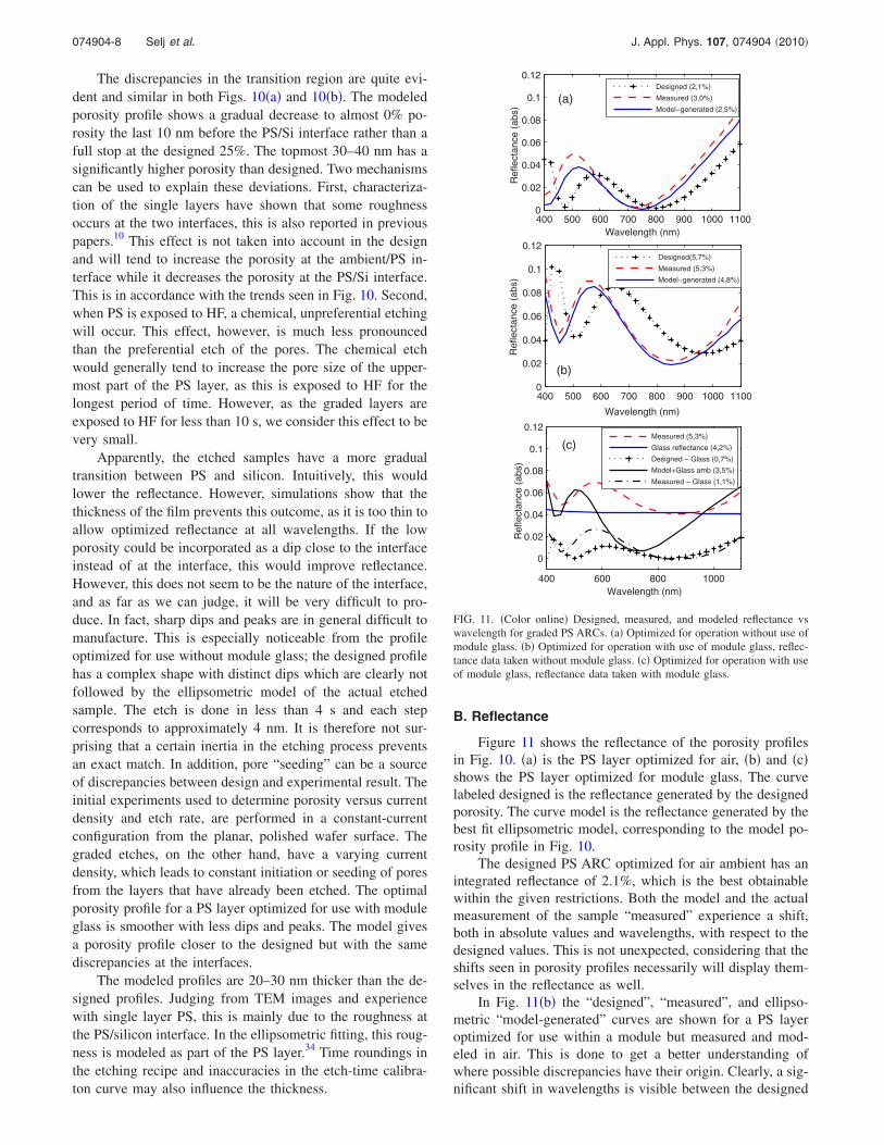
B. Reflectance
Figure 11 shows the reflectance of the porosity profilesin Fig. 10. �a� is the PS layer optimized for air, �b� and �c�shows the PS layer optimized for module glass. The curvelabeled designed is the reflectance generated by the designedporosity. The curve model is the reflectance generated by thebest fit ellipsometric model, corresponding to the model po-rosity profile in Fig. 10.
The designed PS ARC optimized for air ambient has anintegrated reflectance of 2.1%, which is the best obtainablewithin the given restrictions. Both the model and the actualmeasurement of the sample “measured” experience a shift,both in absolute values and wavelengths, with respect to thedesigned values. This is not unexpected, considering that theshifts seen in porosity profiles necessarily will display them-selves in the reflectance as well.
In Fig. 11�b� the “designed”, “measured”, and ellipso-metric “model-generated” curves are shown for a PS layeroptimized for use within a module but measured and mod-eled in air. This is done to get a better understanding ofwhere possible discrepancies have their origin. Clearly, a sig-nificant shift in wavelengths is visible between the designed
400 500 600 700 800 900 1000 11000
0.02
0.04
0.06
0.08
0.1
0.12
Wavelength (nm)
Ref
lect
ance
(abs
)
Designed (2,1%)
Measured (3,0%)
Model−generated (2,5%)
400 500 600 700 800 900 1000 11000
0.02
0.04
0.06
0.08
0.1
0.12
Wavelength (nm)
Ref
lect
ance
(abs
)
Designed(5,7%)
Measured (5,3%)
Model−generated (4,8%)
400 600 800 1000
0
0.02
0.04
0.06
0.08
0.1
0.12
Wavelength (nm)
Ref
lect
ance
(abs
)
Measured (5,3%)
Glass reflectance (4,2%)
Designed − Glass (0,7%)
Model+Glass amb (3,5%)
Measured − Glass (1,1%)
(b)
(a)
(c)
FIG. 11. �Color online� Designed, measured, and modeled reflectance vswavelength for graded PS ARCs. �a� Optimized for operation without use ofmodule glass. �b� Optimized for operation with use of module glass, reflec-tance data taken without module glass. �c� Optimized for operation with useof module glass, reflectance data taken with module glass.
074904-8 Selj et al. J. Appl. Phys. 107, 074904 �2010�

and measured reflectances. The absolute values, however, aresimilar. The designed curve actually has a higher reflectancethan the measured. This is possible because the design isoptimized for module operation, while the resulting reflec-tance is here displayed as it would be in air ambient. Notethe excellent fit between the measured and model-generatedreflectance. Reflectance data are not utilized during the ellip-sometric fitting procedure but generated from the best fitmodel afterwards. The close fit between measured and mod-eled values is, therefore, a strong support of the accuracy ofthe ellipsometric modeling.
In Fig. 11�c�, all curves refer to a PS layer optimized forglass and encapsulated in a module. The measurements showa total integrated reflection of 5.3%, included reflectionsfrom the glass/air interface but excluded absorption-losses inthe glass and EVA. In the designed model, we are not able toinclude reflectance from the front side of the module glass.Glass may readily be used as ambient, but if used as a sepa-rate layer, standing wave interferences arise and complicatethe theoretical reflectance spectrum with sharp oscillations.In actual measurements we do, however, not expect to seesuch oscillations since even the smallest thickness inhomo-geneties are enough to effectively destruct them. Therefore,the generated design spectrum will in effect have subtractedthe glass reflectance “designed-glass”. For direct comparisonwe must do the same for the measured spectrum “measured-glass”. This subtraction has the added benefit of clearly dis-playing the reflectance which actually results from the PS/glass interface. The measured integraded reflectance of thePS ARC is then 1.1%. Note that the integrating sphere setupused for reflectance measurements does not take absorptionin the glass and EVA into account. Using transmission dataof glass41 and EVA �Ref. 42� to correct for absorption effects,the actual reflectance of the PS ARC is �1.4%.
The encapsulated PS sample is too thick to obtain ellip-sometric data. Therefore no model-generated curve is shownin Fig. 11�c�. Simply using the ellipsometric model obtainedwithout glass and adding a glass ambient in the model willnot suffice. The EVA will alter the topmost of the PS layerand an EMA with void as one constituent will no longer beaccurate. For simplicity this is not taken into account in theoriginal design.
The refractive indices of the the specific glass used in themodules are found using ellipsometry and transmission data.The reflectance is then calculated from the refractive indicesusing the WVASE32 software. This is shown in Fig. 11�c� asreference “glass reflectance”. All reflectances are measuredand modeled at an incident angle of 10° to the surface nor-mal and integrated reflections are given in the wavelengthrange 400–1100 nm. The blue part of the terrestrial solarspectrum, 300–400 nm, is not included due to limitations ofthe spectral response unit used for measurements. However,very few rays in this wavelength range actually reach Earth.Therefore, even if the reflectance in the 300–400 nm range isassumed to be high, it modifies the total reflectance by muchless than the standard deviation �0.3� of the reflectance mea-surements of the laminated PS layer. The uncertainties de-scribed by the standard deviation are primarily due to inac-
curacies in the spectral response setup and inhomogenetieson the sample surface.
VII. CONCLUSIONS
By varying current density while all other parameters arekept constant, a broad porosity span �25%−75%+roughness� is available for PS. Exploiting the correspond-ing range of refractive indices, excellent PS ARCs can bedesigned and fabricated within restrictions applying for ap-plication in photovoltaics. Especially when the design incor-porates module glass, excellent ARCs with a total reflectanceof 5.6%, glass included, can be made inexpensively and inless than 6 s. Without glass, an integrated reflectance of�3% is obtained. Important questions such as optimal thick-ness and passivation are still to be addressed before a gradedPS ARC can be implemented in efficient Si solar cells.
ACKNOWLEDGMENTS
Thanks to Dr. T. Wagner at Oriel Laser Optik Technolo-gie GmbH and Dr. M. Kildemo at the Norwegian Universityof Science and Technology for guidance and advice on ellip-sometric modeling. Thanks to M. F. Sunding at University ofOslo for XPS imaging. This work has been funded by theResearch Council of Norway through the project “Thin andhighly efficient silicon-based solar cells incorporating nano-structures,” NFR Project No. 181884/S10.
1R. Bilyalov, L. Stalmans, and L. Schirone, IEEE Trans. Electron Devices46, 2035 �1999�.
2R. R. Bilyalov, R. Lüdemann, W. Wettling, L. Staalmans, J. Poortmans, J.Nijs, L. Schirone, G. Sotgiu, S. Strehlke, and C. Levy-Clemet, Sol. EnergyMater. Sol. Cells 60, 391 �2000�.
3R. Hezel and R. Schoerner, J. Appl. Phys. 52, 3076 �1981�.4A. G. Aberle, Sol. Energy Mater. Sol. Cells 65, 239 �2001�.5B. Sopori, J. Electron. Mater. 32, 1034 �2003�.6D. N. Wrigth, E. S. Marstein, and A. Holt, Double Layer AntireflectiveCoatings for Silicon Solar Cells �IEEE, New York, 2005�.
7D. Bouhafs, A. Moussi, A. Chikouche, and J. M. Ruiz, Sol. Energy Mater.Sol. Cells 52, 79 �1998�.
8V. M. Aroutiounian, K. Martirosyan, and P. Soukiassian, J. Phys. D 37,L25 �2004�.
9S. Uehara, K. Kurose, and T. Matsubara, Phys. Status Solidi A 182, 461�2000�.
10C. C. Striemer and P. M. Fauchet, Phys. Status Solidi 197, 502 �2003�.11K. L. Jiao and W. A. Anderson, Solar Cells 22, 229 �1987�.12S. E. Lee, S. W. Choi, and J. Yi, Thin Solid Films 376, 208 �2000�.13http://www.casaxps.com14H. Lang and P. Steiner, Sens. Actuators, A 51, 31 �1995�.15L. Canham, Properties of Porous Silicon, EMIS Datareviews Series No
18, 1997.16B. Hamilton, Semicond. Sci. Technol. 10, 1187 �1995�.17R. L. Smith and S. D. Collins, J. Appl. Phys. 71, R1 �1992�.18X. G. Zhang, J. Electrochem. Soc. 151, C69 �2004�.19St. Frohnhoff, M. G. Berger, M. Thönissen, C. Dieker, L. Vescan, H.
Münder, and H. Lüth, Thin Solid Films 255, 59 �1995�.20J. Benick, O. Schultz-Wittmann, J. Schön, and S. W. Glunz, Phys. Status
Solidi 2, 145 �2008�.21V. Lehmann, Micro Electro Mechanical Systems, 1996, MEMS ’96, Pro-
ceedings, pp. 1–6, February, 1996 �DOE Scientific and Technical Informa-tion, Washington, DC, 1996�.
22J. Carstensen, M. Christophersen, G. Hasse, and H. Föll, Phys. StatusSolidi A 182, 63 �2000�.
23U. Rossow, U. Frotscher, M. Thonissen, M. G. Berger, S. Frohnhoff, H.Munder, and W. Richter, Thin Solid Films, 255, 5 �1995�.
24L. A. A. Pettersson, L. Hultman, and H. Arwin, Appl. Opt. 37, 4130�1998�.
074904-9 Selj et al. J. Appl. Phys. 107, 074904 �2010�

25D. A. G. Bruggeman, Ann. Phys. 416, 665 �1935�.26D. Kovalev, G. Polisski, J. Diener, H. Heckler, N. Künzner, V. Y. Timosh-
enko, and F. Koch, Appl. Phys. Lett. 78, 916 �2001�.27M. I. Strashnikova, V. L. Voznyi, V. Y. Reznichenko, and V. Y. Gaivoron-
skii, J. Exp. Theor. Phys. 93, 363 �2001�.28L. A. Golovan’, P. K. Kashkarov, and V. Y. Timoshenko, Crystallogr. Rep.
52, 672 �2007�.29C. M. Herzinger, B. Johs, W. A. McGahan, J. A. Woollam, and W. Paul-
son, J. Appl. Phys. 83, 3323 �1998�.30R. M. A. Azzam, N. M. Bashara, and S. S. Ballard, Ellipsometry and
Polarized Light, �1978�, Vol. 31.31J. Rivory, Thin Solid Films 313-314, 333 �1998�.32S. Zangooie, R. Jansson, and H. Arwin, J. Appl. Phys. 86, 850 �1999�.
33K. Kaminska, A. Amassian, L. Martinu, and K. Robbie, J. Appl. Phys. 97,013511 �2005�.
34D. E. Aspnes, J. B. Theeten, and F. Hottier, Phys. Rev. B 20, 3292 �1979�.35C. Pickering, M. I. J. Beale, D. J. Robbins, P. J. Pearson, and R. Greef, J.
Phys. C 17, 6535 �1984�.36C. Wongmanerod, S. Zangooie, and H. Arwin, Appl. Surf. Sci. 172, 117
�2001�.37H. A. MacLeod, Thin-Film Optical Filters, 2nd ed. �Hilger, Bristol, 1986�.38R. Jacobsson, Prog. Opt. 5, 247 �1966�.39D. Poitras and J. A. Dobrowolski, Appl. Opt. 43, 1286 �2004�.40W. H. Southwell, Opt. Lett. 8, 584 �1983�.41Gerhard Menzel GmbH Thermo Fisher Scientific Durchlassigkeit.42Etimex Solar GmbH. Datasheet, December 2008.
074904-10 Selj et al. J. Appl. Phys. 107, 074904 �2010�
Copyright © 2022 FDOKUMEN