Using germanium as a bridge in III-Vs-on-silicon Silicon ...
100
semiconductorTODAY COMPOUNDS & ADVANCED SILICON Vol.11 • Issue 8 • October 2016 www.semiconductor-today.com ISSN 1752-2935 (online) First 60GHz RF SOI switch• Wolfspeed launches 1000V SiC MOSFET Veeco reduces ALD investment •Aixtron sale under review Using germanium as a bridge in III-Vs-on-silicon Silicon carbide enters Formula E Using germanium as a bridge in III-Vs-on-silicon Silicon carbide enters Formula E
-
Upload
khangminh22 -
Category
Documents
-
view
2 -
download
0
Transcript of Using germanium as a bridge in III-Vs-on-silicon Silicon ...

semiconductorTODAYC O M P O U N D S & A D V A N C E D S I L I C O NVol.11 • Issue 8 • October 2016 www.semiconductor-today.com
ISSN 1752-2935 (online)
First 60GHz RF SOI switch•Wolfspeed launches 1000V SiC MOSFETVeeco reduces ALD investment•Aixtron sale under review
Using germanium as abridge in III-Vs-on-silicon Silicon carbide entersFormula E
Using germanium as abridge in III-Vs-on-silicon Silicon carbide entersFormula E

Introducing Veeco’s new TurboDisc® EPIK700™ GaN MOCVD system As global consumption for LED general lighting accelerates, manufacturers need bigger, better MOCVD technology solutions that increase productivity and lower manufacturing costs. The EPIK700 MOCVD system combines Veeco’s award-winning TurboDisc reactor design with improved wafer uniformity, increased productivity and reduced operations expenses to enable a cost per wafer savings of up to 20 percent compared to previous systems. It also features a reactor with more than twice the capacity of previous generation reactors. This increased volume coupled with productivity advancements within the EPIK700 reactor, results in an unmatched 2.5x throughput advantage over previous reactors. Learn how Veeco’s TurboDisc EPIK700 GaN MOCVD system can improve your LED manufacturing process today. The advantage is not just big. It’s EPIK.
Contact us at www.veeco.com/EPIK700 to learn more.
Another breakthrough from Veeco. This time it’s EPIK.
Veeco’s New TurboDisc EPIK700 GaN MOCVD System
Faster LED Adoption
Lower Cost LEDs

www.semiconductor-today.com semiconductorTODAY Compounds&AdvancedSilicon • Vol. 11 • Issue 8 • October 2016
3
contentsEditorial 4
Markets News 6 Gallium demand to grow at 6% annually to 420t in 2020 • COB LEDmarket for lighting rising at 4% CAGR to over $700m in 2021 Microelectronics News 8MACOM & X-Microwave collaborate on faster, easier RF system design• Peregrine unveils first 60GHz RF SOI switches; UK team expands Wide-bandgap electronics News 16SiC enters Formula E • Wolfspeed launches first 1000V SiC MOSFET• Raytheon wins $14.9m Title III contract to enhance GaN process •Mentor Graphics joins WBGi power electronics consortium Materials and processing equipment News 27Aixtron sale blocked • Veeco reducing investment in ALD technologyLED News 36 Epistar quadrupling CSP LED chip capacity • BluGlass and Lumiledsevaluation agreement enters Phase II • Patent lawsuit news Optoelectronics News 52 Osram laser achieves lab record for brilliance • Hamamatsu expands• Canon develops first InP immersion grating • Infinera joins AIMPhotonics • POET expanding in Singapore; partners with Luxmux Optical communications News 58 Renesas launches first laser achieving stable 28G operation at 85°C Photovoltaics News 60 Oxford PV raises £8.7m of Series C funding • Dyesol wins UK grant
Technology focus: Photovoltaics 64InGaN solar cells with positive temperature coefficient
Technology focus: 2D materials 66Two-dimensional GaN with graphene encapsulation
Technology focus: 2D materials 68Electrically driven single-photon emission from atomically thin diodes
Technology focus: Nitride LEDs 70Combatting droop with thick single quantum wells on semi-polar GaN
Technology focus: Nitride lasers 72Reducing laser diode optical leakage with InGaN waveguides
Technology focus: III-Vs on Si — optoelectronics 74Flip-chip hybrid external-cavity laser array on silicon platform
Technology focus: III-Vs on Si — optoelectronics 76Germanium and silicon photonics
Technology focus: Nitride transistors 84Silicon monoxide passivation for gallium nitride transistors
Market focus: GaN power devices 86GaN power device market growing at 86% CAGR to $280m in 2021
Technology focus: GaAs transistors 88Reducing subthreshold swing of gallium arsenide transistors
Technology focus: 2D transistors 90Berkeley-led team fabricates transistor with record 1nm gate
Suppliers’ Directory 92
Event Calendar and Advertisers’ Index 98
Vol. 11 • Issue 8 • October 2016
p13Arralis has won the IT andTelecommunications Award as well asthe overall Innovation of the Year prizefor its 94GHz W-band radar chipset.
p53 Artist’s rendition of new buildingno. 3 at Hamamatsu Photonics’Miyakoda Factory for expanding IRdetector/emitter production.
p90 A Berkeley Lab-led team hasfabricated a transistor with a record1nm-long gate, using a carbon nanotubewith an MoS2 channel.
semiconductorTODAYC O M P O U N D S & A D V A N C E D S I L I C O N
Cover: Japan’s RohmSemiconductor hasintroduced its silicon carbideinverter technologyat the first race ofthe new 2016/2017Formula E season in
Hong Kong. With the start of season 3,Rohm is starting its official partnershipwith the Venturi Formula E team. p19

Following last issue’s coverage of the integration of III-V light-emittingmaterial with silicon photonics (including Intel’s launch in August of its firstSilicon Photonics 100G optical transceiver products) in the article on pages76–82 of this issue we focus on research into how germanium can be used asa ‘bridge’ layer (forming a Ge/Si ‘virtual substrate’) to ease the integrationof compound semiconductor material onto silicon photonic platforms,specifically for infrared light-emission. This even includes a Ge/SiGe-basedLED, since light from germanium has a longer wavelength than that fromsilicon and is hence transmissible by silicon photonic waveguide structures. Conversely, pages 74–75 report research by Oracle that uses flip-chip
bonding for hybrid (rather than monolithic) integration of what it claims is thefirst surface-normal coupled laser array on a silicon-on-insulator photonicsplatform (forming a tunable hybrid external-cavity laser array). Also in this issue we report research on two-dimensional materials.
VerLASE Technologies has been awarded a US patent on using 2D materialsto grow semiconductor structures that can down-convert InGaN-basedblue/violet emitters into any color in the visible part of the spectrum, obviating the use of phosphors and quantum dots (see page 53). In addition, on pages 68–69 we report the use of atomically thin layers of
a transition-metal dichalcogenide (TMD) material (in this case WSe2) as theactive layer in a tunnel-junction device for single-photon emission. Meanwhile, in microelectronics, Berkeley Lab has used another TMD (MoS2)
as a channel material in a transistor with a gate (consisting of a carbonnanotube) with a record short length of just 1nm (see pages 90–91). Although the use of 2D materials in device research is burgeoning, adoption
of 2D (or atomic-layer) technology for commercial production is still earlystage. Deposition and process equipment maker Veeco Instruments hasannounced additional cost-reduction initiatives after deciding to significantlyreduce future investments in its atomic layer deposition (ALD) technologydevelopment (page 30). This follows a delay in timing for revenue realization.Nevertheless, the firm still plans to retain its ALD intellectual property andtechnology capabilities and to continue to assess future market opportunities. Meanwhile, fellow metal-organic chemical vapor deposition (MOCVD) system
maker Aixtron says that Germany’s Federal Ministry of Economics and Energyhas withdrawn the Clearance Certificate (issued on 8 September) for China’sFujian Grand Chip Investment Fund’s proposed offer made in May to acquireAixtron, and announced a reopening of review proceedings (see page 31).Information available to the German Federal Government indicates thatAixtron’s know-how also comprises security-related technologies (in partic-ular for the defense sector) that could be revealed through the acquisition. Fujian Grand Chip (FGC) is held 51% by Chinese businessman and private
investor Zhendong Liu and 49% by Xiamen Bohao Investment Ltd. However,according the New York Times, concerns have a risen regarding possible linksbetween Chinese state investment in both FGC and San’an Optoelectronics(China’s largest LED maker). In early 2016, San’an failed to qualify Aixtron’snew AIX R6 MOCVD system, leading to truncation of a large multi-systemorder and prompting a drop in Aixtron’s share price. Hopefully the ministry’sreview will take weeks rather than months to preclude any further uncertainty. Mark Telford, Editor [email protected]
semiconductorTODAY Compounds&AdvancedSilicon • Vol. 11 • Issue 8 • October 2016 www.semiconductor-today.com
4
editorialsemiconductorTODAYC O M P O U N D S & A D V A N C E D S I L I C O N
Editor Mark TelfordTel: +44 (0)1869 811 577 Cell: +44 (0)7944 455 602 Fax:+44 (0)1242 291 482
E-mail: [email protected]
Commercial Director/Assistant EditorDarren Cummings Tel: +44 (0)121 288 0779Cell:+44 (0)7990 623 395Fax:+44 (0)1242 291 482E-mail: [email protected]
Advertisement SalesDarren Cummings Tel: +44 (0)121 288 0779Cell:+44 (0)7990 623 395Fax:+44 (0)1242 291 482E-mail: [email protected]
Original design Paul Johnsonwww.higgs-boson.com
Semiconductor Today covers theR&D and manufacturing ofcompound semiconductor andadvanced silicon materials and devices(e.g. GaAs, InP and SiGe wafers, chipsand modules for microelectronic andoptoelectronic devices such as RFICs,lasers and LEDs in wireless and opticalcommunications, etc).
Regular issues contain:● news (funding, personnel, facilities,
technology, applications and markets); ● feature articles (technology, markets,
regional profiles); ● conference reports; ● event calendar and event previews; ● suppliers’ directory.
Semiconductor Today (ISSN 1752-2935)is published free of subscription chargein a digital format 10 times per year by Juno Publishing and Media Solutions Ltd,Suite no. 133, 20 Winchcombe Street,Cheltenham GL52 2LY, UK. See: www.semiconductor-today.com/subscribe.htm
© 2016 Juno Publishing and MediaSolutions Ltd. All rights reserved.Semiconductor Today and the editorialmaterial contained within is the copyrightof Juno Publishing and Media Solutions Ltd.Reproduction in whole or in part withoutpermission is forbidden. In most cases,permission will be granted, if the author,magazine and publisher are acknowledged.
Disclaimer: Material published withinSemiconductor Today does not necessarilyreflect the views of the publisher or staff.Juno Publishing and Media Solutions Ltdand its staff accept no responsibility foropinions expressed, editorial errors anddamage/injury to property or persons asa result of material published.
Slicing layers ever thinner


The global market for chip-on-board(COB) LEDs used in lighting appli-cations — including COB productsbelonging to ceramic and EMCpackages — will rise at a compoundannual growth rate (CAGR) ofabout 4% from $580m in 2016 tomore than $700m in 2021, accord-ing to the ‘2016-2021 Global LEDIndustry Demand and Supply Database Report’ by LEDinside (a division of TrendForce). “COB LEDs are mainly for the
commercial lighting market,” notesJoanne Wu, assistant researchmanager at LEDinside. “However,recent technological advances haveimproved the reliability of high-power COB products, allowing themto gradually expand into variousoutdoor applications such as light-ing equipment for mining sites andstreet lighting. COB and high-power LEDs are expected to havecompetitive advantages in thehigh-end lighting applicationsbecause they have advantages thatmid-power LEDs lack in terms ofdesign and brightness,” she adds. International LED suppliers (in
contrast to China-based LED sup-pliers) offer COB product lines thatare wider ranging, notes Wu.“Moreover, they have much higherstandards regarding brightness ofthe light and quality and reliabilityof products,” she adds. “Interna-tional suppliers also control the cru-cial IP related to COB LEDs, so theytend to have more customers andare chosen by major lightingexporters.” China-based LED suppliers on the
other hand offer bargain prices andhave a large domestic market.Also, they are developing COB LEDswith EMC packages. These productsare expected to contribute to therapid growth of revenue related toCOB LEDs for lighting applications.
Japan’s Citizen Electronics toppedthe worldwide revenue ranking ofCOB LED suppliers in 2015, whilethe USA’s Cree took second place.Citizen was able to capture thelargest market share via a verycomprehensive product line strat-egy. Last year, Citizen and Creeinvested heavily in high-brightness,bargain-priced COB products forspecific applications, such as the10W-and-under segment of theindoor commercial lighting marketand the 50W-and-above segmentsof both the industrial and outdoorlighting markets. The two companiesshould also see significant growthin COB LED revenue in 2016 asthey take their products into thehorticultural lighting market. Sharp and Bridgelux shared third
place in the 2015 COB LED revenueranking. With dual-color productsand valuable patents, Sharp wasable to push its COB LEDs into thecommercial and medical lightingmarkets.Bridgelux’sCOB prod-ucts, whichare mainlyfor industriallighting, areexceptionalin quality,
given their prices, reckons LEDinside. Lumileds and Nichia were tied at
fifth place in the 2015 ranking. Bygreatly expanding their product lines,both firms were able to significantlyincrease their COB LED revenues.Both suppliers are launching moreproducts in second-half 2016 andare likely to again post large annualincreases in their COB LED revenues. Since 2014, Samsung has been
focusing on developing COB prod-ucts and making inroads into thelighting market. Consequently, thesupplier significantly grew its COBLED revenue in 2015 and becamethe seventh largest supplier in theannual ranking. “China-based suppliers such as
Sunpu and LED Teen have beenjust as active as their internationalcounterparts developing COB prod-ucts,” notes Wu. “Sunpo climbed toeighth place in the 2015 COB rev-enue ranking on the back of strongsales of its full-spectrum productsfor the horticultural applicationmarket. LED Teen has always beenfocusing on developing COB LEDsand has grown rapidly in recentyears,” she adds. “This year, LEDTeen has improved its position inthe high-end commercial lightingmarket by successfully launchingits high-density, high-color render-ing COB LED arrays.” Likewise, US-based LED maker
Luminus Devices, which wasacquired by China’s San’an Opto-electronics in the 2013, has posi-tioned itself as another supplier inthe high-end commercial lightingmarket. Luminus Device currentlyhas a production site in Xiamen,China. The plant is undergoingcapacity expansion and will be animportant revenue contributor, concludes the report. www.ledinside.com
Recenttechnologicaladvances haveimproved thereliability of high-power COB products
semiconductorTODAY Compounds&AdvancedSilicon • Vol. 11 • Issue 8 • October 2016 www.semiconductor-today.com
6
newsCOB LED market for lighting applications to grow at4% CAGR from $580m in 2016 to over $700m in 2021 Citizen and Cree seeing significant growth in horticultural market
1 Citizen Electronics2 Cree3 Sharp3 Bridgelux5 Lumileds5 Nichia7 Samsung 8 Sunpu9 LED Teen10 Luminus Devices
Top COB LED suppliers byrevenue in 2015.

News: Markets
www.semiconductor-today.com semiconductorTODAY Compounds&AdvancedSilicon • Vol. 11 • Issue 8 • October 2016
7
Overall revenue for the powersemiconductor market globally fellby 2.6% to $34bn in 2015, due primarily to macroeconomic factorsand application-specific issues,according to IHS Markit’s ‘Power Semiconductor Market ShareReport — 2016’ (which this yearincludes power ICs for the first time,as well as discrete power semicon-ductors and power semiconductormodules). Specifically, discretepower semiconductor product revenue declined 10.1% and powermodule revenues fell by 11.4%,while power integrated circuit (IC)revenue rose by 4.5%. As part of IHS Markit’s Power
Semiconductor Intelligence Service,the report identifies Infineon Tech-nologies as the leading powersemiconductor manufacturer lastyear, with 12% of the market,Texas Instruments with 11% andSTMicroelectronics with 6%. “While Texas Instruments
previously led the market in 2014,
the company was overtaken byInfineon Technologies in 2015, following its acquisition of International Rectifier and LS PowerSemitech,” says senior analystRichard Eden. “Infineon was theleading global supplier of both discrete power semiconductors and power modules, and thefourth-largest supplier of powermanagement ICs,” he adds. “Infineon has been the leading supplier of discretes for severalyears, but overtook Mitsubishi Electric to lead the power module market for the first time in 2015,again, due to the International Rectifier and LS Power Semitechacquisitions.” According to the report, while
Infineon Technologies’ acquisitionof International Rectifier was thelargest acquisition last year, severalother deals also changed the terrain of the power semiconductormarket landscape. In 2015, MediaTek acquired RichTek,
Microchip acquired Micrel, and NXP Semiconductors acquiredFreescale Semiconductor. In addition,NXP Semiconductors created WeEnSemiconductors, a joint venturewith Beijing JianGuang Asset Management Co. Ltd (JAC Capital).Also, CSR Times Electric mergedwith China CNR Corp to form CRRCTimes Electric, and ROHM Semi-conductor acquired Powervation. “Companies were active in
acquisitions for several reasons —especially the low financing cost inmultiple regions of the world, whichmeant that borrowing rates in theUnited States and European Centralbank were nearly zero,” notes senior analyst Jonathan Liao. “In addition, the acquiring companytypically increases its revenues andmargins by taking the acquiredcompany’s existing customers andsales without incurring marketing,advertising and other additionalcosts.” https://technology.ihs.com
Infineon tops power semiconductor market, followed by Texas Instruments and STMicroelectronics,after 2.6% decline to $34bn in 2015
The market for gallium in semiconductor/semi-insulatingapplications is set to rise at 6%annually to about 420 tons in 2020as general illumination shifts awayfrom incandescent-filament andfluorescent lamps to light-emittingdiodes, according to the report‘Gallium: Global Market Trends andProspects’ from Merchant Research& Consulting Ltd. In particular, the usage of gallium
in LEDs for general lighting is set togrow at 16% per year. Meanwhile,the usage of gallium in integratedcircuits is projected to remain mostprominent, but to drop to 43% ofthe total. Consumption in LEDs for
backlighting applications is unlikelyto see robust growth due to theincreased technical effectiveness ofLEDs. Despite the overall growth, the
gallium marketsees continuingoversupply.Between 2010and 2013 Chinese capacityfor production ofprimary galliumincreased threefold inanticipation ofsurgingdemand for
gallium nitride (GaN) LEDs forbacklighting of liquid-crystal display(LCD) panels used in tablets, cell phones and TVs. The worldwidetransition to LED general lightingover the next five years is poised torestore some balance to the galliummarketplace, but supply will likelyremain more than adequate. Japan is poised to take the lead in
gallium consumption, although itsmarket share will fall from 47% in2014 to just over 40% in 2020,forecasts the report. Meanwhile,due largely to the increased usagein lighting, China’s share is likely tosurge to 35%. www.marketpublishers.com
Gallium demand to grow at 6% annually to 420t in 2020Growth of 16% for LEDs in general lighting to outweigh usage in ICsfalling to 43% of market
The worldwidetransition toLED generallighting overthe next fiveyears is poisedto restore somebalance to thegalliummarketplace

News: Microelectronics
semiconductorTODAY Compounds&AdvancedSilicon • Vol. 11 • Issue 8 • October 2016 www.semiconductor-today.com
8
Skyworks Solutions Inc of Woburn,MA, USA (which manufactures analog and mixed-signal semicon-ductors) says that its portfolio of newSkyOne Ultra 2.0 and SkyLiTE 2.0front-end modules are supportinghigh-power user equipment (HPUE)for mobile devices. HPUE is a special class of user
equipment for LTE cellular networksthat improves cell range and increasecoverage. Skyworks says that itscomplete RF front-end systemsleverage its proprietary SkyBluetechnology to deliver enhancedoutput power and meet HPUE certification requirements fromTDD carriers. SkyOne Ultra 2.0HPUE-compliant solutions are currently shipping at several customers while the SkyLiTE 2.0HPUE-compliant devices will beavailable for ramps commencing in2017. According to the latest reportfrom the Global mobile SuppliersAssociation (GSA), 71 operators in43 countries have commerciallylaunched LTE service using TDDmode, with the unpaired spectrumexpected to see growth in allregions. “With smartphones supporting
upwards of 20 frequency bands andmore than 30 carrier aggregation
combinations, there is an increas-ing need for innovative front-endsolutions that address high-performance, cellular TDD-LTEapplications,” says VP of sales &marketing Carlos Bori. “Leveragingour systems expertise, Skyworks iscollaborating with carriers andOEMs to develop highly integrateddevices that solve increasinglycomplex RF challenges, meet themost demanding standards, andprovide unparalleled performance,”he adds. “HPUE significantly increases
TDD-LTE Band 41 coverage and isan important innovation that willbenefit the global TDD-LTE ecosys-tem,” comments Dr Ron Marquardt,VP of technology at Sprint. "HPUEwill further unlock the advantagesof the 2.5GHz spectrum, particu-larly as consumers require morecapacity and faster data speeds.” SkyOne Ultra 2.0 is a highly
integrated, single LTE SKU (stockkeeping unit) solution that solvesharmonically related carrier aggre-gation challenges through designwhile delivering high linear RFpower as well as power-added efficiency. Skyworks claims that the platform not only improves performance in terms of power out-
put and system efficiency, it alsodelivers this performance in themost compact size commerciallyavailable, supporting 22 bands inless than 240mm2. SkyLiTE 2.0 is a highly integrated
module that incorporates theamplification, switching, Wi-Fi fil-tering and coupler functionalityrequired to support all majorFDD/TDD bands. With the additionof external duplexers, this family ofsolutions provides OEMs with ascalable and reconfigurable front-end system suitable for marketsworldwide. SkyBlue technology delivers enve-
lope tracking (ET)-like system effi-ciency, but with a far simplerimplementation method comparedwith traditional ET systems, saysSkyworks. Utilizing the more con-ventional average power tracking(APT)-like approach, SkyBlue control is intuitive and has a rapidlearning curve relative to ET calibration requirements, the firmadds. www.skyworksinc.com/Products/622 www.skyworksinc.com/Products/1031 www.skyworksinc.com/Products_SkyBlue.aspx
Skyworks’ SkyOne Ultra 2.0 and SkyLiTE 2.0 front-endmodules with SkyBlue technology addressing demandfor increased power and data coverage
Skyworks Solutions Inc of Woburn,MA, USA (which makes analog andmixed-signal semiconductors) hasintroduced a family of GPIO-controlled, high-performance RFcellular switches for LTE and GSMapplications. The SKY13581-676LFsingle-pole, double-throw (SP2T),SKY13582-676LF single-pole,triple-throw (SP3T) andSKY13626-685LF single-pole,four-throw (SP4T) are for LTE,while the SKY13597-684LF (SP4T)is for GSM.
The new family of switches issuitable for smartphones, datacards and MiFi hotspot applications.The devices are designed to operate over the complete cellularfrequency range including supportfor Band 42 and Band 43 (up to3.8GHz), allowing the use of onepart for all band requirements.They also feature low insertion lossfor higher transmission efficiencyand what is claimed to be excellentharmonic performance withimproved receiver sensitivity.
The SKY13581-676LF,SKY13582-676LF and SKY13626-685LF share a common layout andare pin-to-pin, footprint compati-ble, enabling faster developmenttime. www.skyworksinc.com/Product/3366/SKY13581-676LF www.skyworksinc.com/Product/3191/SKY13582-676LF www.skyworksinc.com/Product/3368/SKY13626-685LF www.skyworksinc.com/Product/3367/SKY13597-684LF
Skyworks launches family of GPIO-controlled RF cellular switches


News: Microelectronics
semiconductorTODAY Compounds&AdvancedSilicon • Vol. 11 • Issue 8 • October 2016 www.semiconductor-today.com
10
MACOM Technology Solutions Inc ofLowell, MA, USA (which makessemiconductors, components andsubassemblies for analog RF,microwave, millimeter-wave andphotonic applications) and modularsystem design firm X-Microwave LLCof Round Rock, TX, USA haveannounced the availability of MACOM-based RF components for use withX-Microwave’s online simulationand prototyping platform. Pre-configured with MACOM’s MMICs,the drop-in and cascadable compo-nents (X-MWblocks) enable design-ers to quickly and easily architectmodular, end-to-end RF systems. MACOM’s support for the X-Microwave
platform equips designers to takeadvantage of its MMIC performance,with the added ability to inter-connect hundreds of compatible,
pre-characterized X-MWblock components with solderless, build-ing block flexibility. This reducesevaluation and design complexityand enables designers to acceleratetheir time to market, says MACOM.With this collaboration, X-Microwaveusers can now take advantage of abroad selection of MACOM MMICs,spanning amplifiers, mixers, frequency multipliers, octave-bandvoltage-controlled oscillators (VCOs),RF switches, voltage variable atten-uators and phase shifters. “Through our collaboration with
X-Microwave, designers now havethe ability to leverage all of thesebenefits in a manner that can dra-matically accelerate their systemprototyping and shorten designcycles,” says Graham Board, MACOM’ssenior director, RF and Microwave.
“X-Microwave is committed tooptimizing the design process forRF engineers through every phaseof the development process,” saysX-Microwave’s president & CEOJohn Richardson. “With the additionof MACOM MMICs to our compo-nent ecosystem, X-Microwaveusers are assured leading-edge RFperformance and quality from theforemost innovator in the RF andmicrowave industry,” he adds. MACOM showcased its new portfo-
lio of MMICs and its collaborationwith X-Microwave at EuropeanMicrowave Week (EuMW 2016) inLondon, UK (4–6 October). www.eumweek.comwww.xmicrowave.com/products/by-manufacturer/macom-mmics-x-mwblocks www.macom.com
MACOM and X-Microwave collaborate to enablefaster, easier design of RF systems X-Microwave’s online simulation and prototyping platform to offerbuilding blocks pre-configured with MACOM’s MMICs
At European Microwave Week(EuMW 2016) in London, UK (4–6 October), MACOM debuted27 new monolithic microwaveintegrated circuits (MMIC) productscomprising what is claimed to bethe industry’s most extensive portfolio of DC–100GHz MMICs fortest & measurement, SatCom,aerospace & defense, wired broad-band, and industrial, scientific &medical (ISM) applications. MACOM says that, leveraging
foundry technologies and propri-etary in-house processes, it haspioneered a new class of high-performance MMICs spanningproduct categories from amplifiers,frequency converters and controlproducts to frequency sources anddetectors, encompassing the entireblock diagram from signal genera-tion, amplification and conditioningto conversion and monitoring. The new MMIC families comprise:
● Gain block & low-noise amplifiers — Two wideband amplifiers fullymatched and current-adjustableamplifier solutions for multi-marketapplications; — Family of low-noise amplifiersproviding performance and versatility enabling acceleratedtime-to-market. ● Wired broadband amplifiersFamily of amplifiers designedspecifically for DOCSIS 3.1 CATVinfrastructure applications requiringhigh gain, superior linearity andlow noise figure. ● Wideband power amplifiersHigh-power MMIC amplifiers covering DC–22GHz for test &measurement, electronic warfare,and radar applications. ● SatCom power amplifiersHigh-linearity family of poweramplifiers for SatCom applicationsfeaturing a highly integrated L-banddevice supporting longer battery life.
● Voltage-controlled oscillatorsOctave-band VCOs suited to test &measurement, aerospace & defense,and communications systems. “Continued consolidation in the
semiconductor industry has disrupted the MMIC supplierecosystem and left customers withfewer credible, reliable sources forhigh-performance MMICs,” statesGraham Board, senior director,Multi-Market Products. “MACOM ismeeting this challenge head on byincreasing our investment inadvanced MMIC technologies andaggressively expanding our MMICproduct portfolio. As the only pure-play RF, microwave and millimeter-wave supplier with a proven heritageof semiconductor industry leadership— built over six-decades — MACOMis committed to being the trusted,long-term supplier of choice forthe next generation of high-performance MMICs.”
MACOM debuts 27 new DC–100GHz MMICs

News: Microelectronics
www.semiconductor-today.com semiconductorTODAY Compounds&AdvancedSilicon • Vol. 11 • Issue 8 • October 2016
11
Fairview Microwave Inc of Allen, TX,USA, which supplies on-demandmicrowave and RF components, isdebuting a new product family ofseven unique models of IQ mixermodels with RF and LO frequencybands ranging from 4GHz to 38GHzand in-phase and quadrature IFbandwidths ranging from DC to4.5GHz. The new monolithic microwave
integrated circuit (MMIC) IQ mixers(IQ modulators) utilize galliumarsenide (GaAs) MESFET processtechnology that integrates a pair ofmatched double-balanced mixercells, a 90° hybrid and a 0° split-ter/combiner that is said to produceexceptional amplitude and phasebalance performance. This level ofintegration offers size and perform-ance advantages compared withdiscrete module assemblies. With the addition of an external
90° IF hybrid module, these IQmixers can be used as either a single-sideband up-converter mixeror an image reject down-converter
mixer. Image rejection and sidebandsuppression can reduce overall system cost and complexity byremoving the need for pre-selectionfiltering. Typical applications includepoint-to-point and point-to-multipointradio, VSAT, military radar, electronic warfare, satellite com-munications, test equipment, andsensors. Performance as an image reject
mixer (IRM) includes low conver-sion loss that ranges from 7.5dBm
to 10dBm, highimage rejectionup to 35dB typi-cal, and LO-to-RFisolation as highas 42dB typical.The IQ mixerdesigns offer linearity withinput 1dB com-pression as highas +20dB typicaland input IP3 ashigh as +35dBtypical. LO drive
power ranges from +15dBm to+19dBm. The compact and rugged drop-in
package designs are hermeticallysealed with field-replaceable con-nectors and are guaranteed to meetMIL-STD-883 test conditions forhumidity and temperature cycle. All seven models are available
from stock and available for imme-diate shipment. www.fairviewmicrowave.com/rf-products/iq-mixers.html
Fairview debuts new line of GaAs MMIC IQ mixers
Pasternack Inc of Irvine, CA, USA(which makes both passive andactive RF, microwave and millime-ter-wave products) has launched aseries of active frequency multipli-ers that simplify system designs byoffering high output power levels. The active frequency multipliers
are key building block componentsused in local oscillator (LO) chainsfor radar, communication receiversand frequency sources to extendfrequencies and achieve optimalperformance. The firm adds thatthey support multiple markets andapplications including electronicwarfare, electronic countermea-sures, point-to-point radio, VSATradio, test instrumentation andtelecom infrastructure. The PE88X-series active frequency
(x2) multipliers double input
frequencies ranging from 4GHz to23GHz up to desirable millimeter-wave output frequencies from8GHz to 46GHz. The new designsuse highly efficient gallium arsenide(GaAs) pseudomorphic high-elec-tron-mobility transistor (pHEMT)technology with integrated amplifiersthat produce high output powerlevels up to +17dBm with what isclaimed to be excellent fundamen-tal and harmonic suppression. Thiscan eliminate the need for an
external LO buffer amplifier stageand additional support circuitry. The active frequency multipliers
require a single +5V DC supply.Input/output RF ports are matchedfor 50Ω and are DC blocked. Thecompact drop-in package assem-blies are hermetically sealed andsupport field-replaceable 2.92mmconnectors. All models are RoHS-and Reach-compliant and designedto meet MIL-STD environmentaltest conditions. The active frequency multipliers are
in-stock and ready for immediateshipment. “Active multipliers usually require long manufacturingcycles, but Pasternack offers allthree models ready to ship right offthe shelf,” notes active componentsproduct manager Tim Galla. www.pasternack.com
Pasternack launches series of GaAs pHEMT MMICactive frequency multipliers spanning 8–46GHz
Fairview’s new line ofGaAs MMIC IQ mixers
News: Microelectronics
semiconductorTODAY Compounds&AdvancedSilicon • Vol. 11 • Issue 8 • October 2016 www.semiconductor-today.com
12
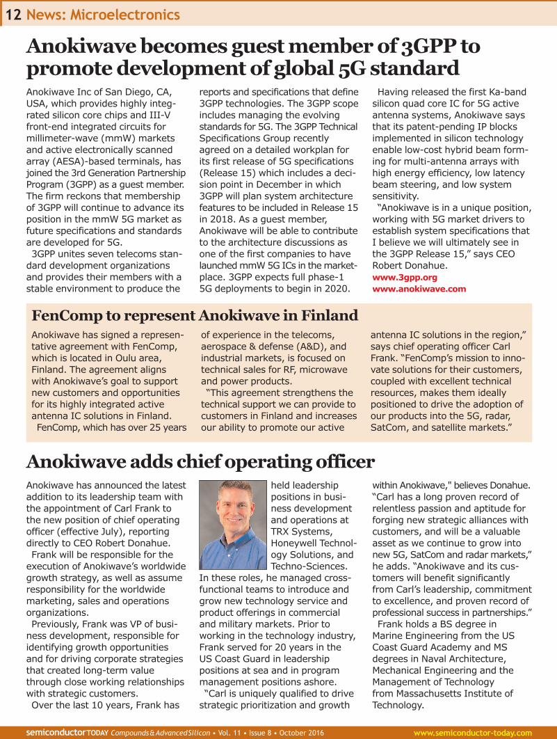
Anokiwave has announced the latestaddition to its leadership team withthe appointment of Carl Frank tothe new position of chief operatingofficer (effective July), reportingdirectly to CEO Robert Donahue. Frank will be responsible for the
execution of Anokiwave’s worldwidegrowth strategy, as well as assumeresponsibility for the worldwidemarketing, sales and operationsorganizations. Previously, Frank was VP of busi-
ness development, responsible foridentifying growth opportunitiesand for driving corporate strategiesthat created long-term valuethrough close working relationshipswith strategic customers. Over the last 10 years, Frank has
held leadershippositions in busi-ness developmentand operations atTRX Systems, Honeywell Technol-ogy Solutions, andTechno-Sciences.
In these roles, he managed cross-functional teams to introduce andgrow new technology service andproduct offerings in commercialand military markets. Prior to working in the technology industry,Frank served for 20 years in the US Coast Guard in leadership positions at sea and in programmanagement positions ashore. “Carl is uniquely qualified to drive
strategic prioritization and growth
within Anokiwave," believes Donahue.“Carl has a long proven record ofrelentless passion and aptitude forforging new strategic alliances withcustomers, and will be a valuableasset as we continue to grow intonew 5G, SatCom and radar markets,”he adds. “Anokiwave and its cus-tomers will benefit significantlyfrom Carl’s leadership, commitmentto excellence, and proven record ofprofessional success in partnerships.” Frank holds a BS degree in
Marine Engineering from the USCoast Guard Academy and MSdegrees in Naval Architecture,Mechanical Engineering and theManagement of Technology from Massachusetts Institute ofTechnology.
Anokiwave has signed a represen-tative agreement with FenComp,which is located in Oulu area, Finland. The agreement alignswith Anokiwave’s goal to supportnew customers and opportunitiesfor its highly integrated activeantenna IC solutions in Finland. FenComp, which has over 25 years
of experience in the telecoms,aerospace & defense (A&D), andindustrial markets, is focused ontechnical sales for RF, microwaveand power products. “This agreement strengthens the
technical support we can provide tocustomers in Finland and increasesour ability to promote our active
antenna IC solutions in the region,”says chief operating officer CarlFrank. “FenComp’s mission to inno-vate solutions for their customers,coupled with excellent technicalresources, makes them ideallypositioned to drive the adoption ofour products into the 5G, radar,SatCom, and satellite markets.”
FenComp to represent Anokiwave in Finland
Anokiwave Inc of San Diego, CA,USA, which provides highly integ-rated silicon core chips and III-Vfront-end integrated circuits formillimeter-wave (mmW) marketsand active electronically scannedarray (AESA)-based terminals, hasjoined the 3rd Generation PartnershipProgram (3GPP) as a guest member.The firm reckons that membershipof 3GPP will continue to advance itsposition in the mmW 5G market asfuture specifications and standardsare developed for 5G. 3GPP unites seven telecoms stan-
dard development organizationsand provides their members with astable environment to produce the
reports and specifications that define3GPP technologies. The 3GPP scopeincludes managing the evolvingstandards for 5G. The 3GPP TechnicalSpecifications Group recentlyagreed on a detailed workplan forits first release of 5G specifications(Release 15) which includes a deci-sion point in December in which3GPP will plan system architecturefeatures to be included in Release 15in 2018. As a guest member, Anokiwave will be able to contributeto the architecture discussions asone of the first companies to havelaunched mmW 5G ICs in the market-place. 3GPP expects full phase-15G deployments to begin in 2020.
Having released the first Ka-bandsilicon quad core IC for 5G activeantenna systems, Anokiwave saysthat its patent-pending IP blocksimplemented in silicon technologyenable low-cost hybrid beam form-ing for multi-antenna arrays withhigh energy efficiency, low latencybeam steering, and low systemsensitivity. “Anokiwave is in a unique position,
working with 5G market drivers toestablish system specifications thatI believe we will ultimately see inthe 3GPP Release 15,” says CEORobert Donahue. www.3gpp.org www.anokiwave.com
Anokiwave adds chief operating officer
Anokiwave becomes guest member of 3GPP topromote development of global 5G standard

News: Microelectronics
www.semiconductor-today.com semiconductorTODAY Compounds&AdvancedSilicon • Vol. 11 • Issue 8 • October 2016
13
At the Irish Times InnovationAwards ceremony at the RoyalHospital Kilmainham in Dublin on 5 October, Arralis Ltd of Limerick,Ireland — which has a design cen-ter in Belfast and manufactures RF,microwave and millimetre-wavedevices, modules and antennas up to and beyond 110GHz (the W-band) for aerospace/satelliteand security markets — won the IT and Telecommunications Awardas well as the overall prize forInnovation of the Year for its94GHz radar chipset. Arralis’ 94GHz radar chipset has
a wide range of applications including aiding unmanned landingsby spacecraft, drone guidance systems, air defence systems, airport radar and driverless cars,as well as Internet and next-generation 5G telecoms.
The awards ceremony showcasedIreland’s top innovative talent invarious sectors after receivingapplications from more than
300 companies. Theevent was attended bymore than 220 peopleincluding Mary MitchellO’Connor, Ireland’s Minister for Job, Enter-prise and Innovation. As overall winner,
Arralis also will receive acommunications andadvertising package fromThe Irish Times that isworth in excess of€150,000, as well as aUniversity College Dublin(UCD) Smurfit BusinessSchool scholarship for an Executive Educationprogram that will
commence in 2017. www.irishtimes.com/business/ul-based-arralis-wins-innovation-of-the-year-1.2818361
Arralis wins The Irish Times Innovation of the Year Award 2016
Arralis Ltd of Limerick, Ireland,which designs and manufacturesRF, microwave and millimetre-wavedevices, modules and antennas upto and beyond 110GHz (the W-band) for aerospace and securitymarket, has added new monolithicintegrated circuit (MMIC) devices toits product range. The new poweramplifier, image cancellation mixerand variable attenuator come inresponse to new advance systemrequirements, says the firm. Power amplifier The TU-W1330305 is a 4-stageMMIC power amplifier that coversfrequencies of 92–96GHz. It pro-vides up to 20dB of flat, stablegain, and a power output of morethan 18dBm from a 4V supply volt-age and low current of just 210mA.Image cancellation MMIC mixer(92–96GHz) The TU-W1340310 is an I/Q MMICdiode mixer with integrated quad-rature coupler for single-sidebandup-converter operation. Fabricatedusing gallium arsenide (GaAs)Shottky diode technology, it is
designed for output frequencies of92–96GHz using either fixed IF andvarying LO (86–90GHz) or fixed LOand varying IF (2–6GHz) signals.The circuit employs a double rat raceconfiguration to effectively cancelimage signals without filtering andoffers what is claimed to be supe-rior signal-to-noise performance. GaAs pHEMT MMIC attenuator/SPST switch (90–100GHz) The TU-W1401601 is a GaAs pseudo-morphic high-electron-mobilitytransistors (pHEMTs) diode basedsingle-pole single-throw (SPST)
switch and variable attenuator witha single input and output. Theattenuation value can be adjustedto any value within the specifiedattenuation range. The chip ismanufactured on a 50μm substratewith 100μm gate length. All bondpads and the die underside are goldplated. The control voltage rangesfrom +1.5V to –1.5V (the lattergiving maximum attenuation). A packaged version of each device
is also available with WR10 wave-guide input and output on request. “We recently launched the world’s
first W-band up- and down-converters,” said chief technologyofficer Mike Gleaves, speaking atEuropean Microwave Week (EuMW 2016) in London, UK. “We expect the same success with these new devices”. Arralis displayed products including smartbeam-steering antenna technology,new communications and radarmodules, and a unique GNSSantenna with a very low SWaPspecification. www.arralis.com
Arralis launches new W-band MMICs
Pictured at the The Irish Times InnovationAwards presentation: Eamonn Boland, Marie Bourke, Barry Lunn, Valerie Somers andDenver Humphrey of Arralis.

News: Microelectronics
semiconductorTODAY Compounds&AdvancedSilicon • Vol. 11 • Issue 8 • October 2016 www.semiconductor-today.com
14
Peregrine Semiconductor Corp ofSan Diego, CA, USA — a fablessprovider of radio-frequency integrated circuits (RFICs) basedon silicon-on-insulator (SOI) —says that its UK team has movedinto a larger office at 1420 ArlingtonBusiness Park in Theale, Berkshire(in the heart of the Thames Valley).The new 4600ft2 office quadruplesthe working area and laboratoryspace (including two fully equipped
labs) to better accommodate theUK team’s 90% growth since Pere-grine’s acquisition by Japan'sMurata in December 2014. “Our team had outgrown our old
facility — both in seating capacityand in lab space to accommodatenew product development,” saysMark Moffat, managing director ofPeregrine Semiconductor Europe.“Our new home not only bettersuits our current team, but it has
the capacity for our projectedgrowth,” he adds. “With a primelocation in the Thames Valley, weare able to tap into the abundanceof talent in this region and build ateam that is driving Peregrine’sgrowth in areas like 5G and powermanagement.” In addition to the UK office, Pere-
grine has offices in ArlingtonHeights, Illinois; Seongnam-si,South Korea; and Shanghai, China.
Peregrine’s UK team moves into larger office Working area and lab space quadrupled to accommodate 90% growth in two years
Peregrine Semiconductor haslaunched the UltraCMOS PE45361monolithic 100W power limiter.The next generation in Peregrine’spower limiter product family, thePE45361 builds on the firm’s 50WUltraCMOS power limiters and addshigher pulsed power handling, a lower limiting threshold and positive threshold control. UltraCMOS power limiters provide
a monolithic alternative to discrete,PIN-diode limiters based on gallium-arsenide (GaAs) technol-ogy and protect devices againstexcessive RF power, intentionaljamming and ESD events. ThePE45361 is said to deliver reliableand repeatable power protectionto sensitive low-noise receivers fortest & measurement equipmentand wireless-infrastructure trans-ceivers. “Peregrine’s monolithic power
limiters offer our customers anovel and robust approach toexcessive RF power protection,”says director of marketing KinanaHussain. “The introduction of thePE45361 builds upon the key RFperformance and bill of materials(BOM) cost advantages of ourUltraCMOS limiters, while providing100W power handling and low limiting threshold to protect sensi-tive low-noise amplifiers (LNAs).” Compared with PIN diodes, it is
claimed, UltraCMOS power limitersprovide a 10–100x improvementin response-and-recovery time,deliver 10–40dB linearity (IIP3)improvement and offer a 20ximprovement in ESD protection. In addition, UltraCMOS power limiters are 8x smaller than theboard space required by PIN-diodesolutions, the firm adds. Finally,the limiting threshold can beadjusted through a low-currentvoltage control pin (VCTRL), eliminating the need for externalcomponents such as DC blockingcapacitors, RF choke inductors andbias resistors. Like other UltraCMOS power lim-
iters, the PE45361 features twooperating modes — power limitingand power reflecting — to maxi-mize performance and flexibility.These modes can be selectedthrough the programmable VCTRL
pin. In power-limiting mode, the
device is invisible to theload. When the incomingRF signal power exceedsthe limiting thresholdset through the VCTRL pin,the device limits the inputRF power. Power-reflect-ing mode is used in moreextreme conditions, andthe device reflects mostof the incident powerback to the source.
Covering a wide frequency rangefrom 10MHz to 6GHz, the PE45361power limiter provides power protection for high-performance,power-limiting applications. It fea-tures a high pulsed power handlingup to 50dBm and 100W, anadjustable limiting threshold from5dBm to 13dBm and a positivethreshold control from 0V to 0.3V.The PE45361 delivers low insertionloss of 0.95dB at 6GHz and highreturn loss of 15dB at 6GHz (and0.5dB and 20dB, respectively, at3GHz). With a fast response timeof 1ns and a speedy recovery timeof 20ns, it exhibits high linearity of37dBm IIP3 and ESD protection of3kV HBM. Samples and evaluation kits
are available now. Offered in acompact 12-lead 3mm x 3mmQFN package, the PE45361 is$4.80 each for 10,000-unit orders. www.psemi.com
Peregrine launches monolithic 100W RF SOI power limiter
News: Microelectronics
www.semiconductor-today.com semiconductorTODAY Compounds&AdvancedSilicon • Vol. 11 • Issue 8 • October 2016
15
Peregrine Semiconductor Corp ofSan Diego, CA, USA — a fablessprovider of radio-frequency integrated circuits (RFICs) basedon silicon-on-insulator (SOI) — haslaunched the UltraCMOS PE42525and PE426525, which are claimedto be the first RF SOI switches tooperate up to 60GHz. The firm saysthat the two switches significantlyextend its high-frequency portfoliointo frequencies previously domi-nated by gallium arsenide (GaAs)technology. Supporting a wide frequency
range from 9kHz to 60GHz, thePE42525 and PE426525 are reflectivesingle-pole double-throw (SPDT) RF switches delivering a fastswitching speed of 8ns and RFTRISE/TFALL time of 4ns, and lowpower consumption of 450nA. At 50GHz, the PE42525 andPE426525 exhibit high port-to-portisolation of 38dB, low insertion lossof 1.9dB, high power handling,
high linearity, and ESD protectionof 2kV HBM. The PE426525 has anextended temperature range thatspans –55°C to +125°C. The PE42525 is suitable for
test & measurement equipment,microwave-backhaul solutions andhigher-frequency switching in 5G systems. The PE426525 has an extended temperature range, making it suited to harsh-environ-ment applications such oil & gasexploration and other industrialmarkets. “From 26.5GHz to 40GHz and now
60GHz, Peregrine’s high-frequencyportfolio continues to reach frequencies and performance levelspreviously considered unattainablein RF SOI,” says director of marketing Kinana Hussain. “ThePE42525 and PE426525 are proofthat RF SOI can deliver a high-performing, reliable and fastswitching solution at microwavefrequencies. As more applications
demand higher-frequency products,Peregrine will continue to breakmore barriers in RF SOI.” The new 60GHz switches join
Peregrine’s high-frequency productportfolio, which includes multipleswitches, an image-reject mixer,and monolithic phase and ampli-tude controllers (MPACs). Its proprietary UltraCMOS technologyplatform enables these products toreach high frequencies withoutcompromising performance or reliability, the firm adds. The PE42525 and PE426525 are
each available as a flip-chip diewith 500μm bump pitch — reckoned to be the best form factorfor high-frequency performance, as it eliminates performance variations due to wire-bond length. Samples and evaluation kits are
available now. For 1000-unit orders,the PE42525 die costs $40 eachand the PE426525 $48 each. www.psemi.com
Peregrine unveils first 60GHz RF SOI switches CMOS-based high-frequency portfolio extended from 40GHz to 60GHz
Peregrine Semiconductor Corp ofSan Diego, CA, USA — a fablessprovider of radio-frequency integ-rated circuits (RFICs) based on silicon-on-insulator (SOI) — saysthat its UltraCMOS PE42723 high-linearity RF switch has won anECN IMPACT Award in the marketdisruptor category. In addition, the PE42723 switch was named afinalist in the microwaves & RFcategory, and the PE29100 gallium nitride (GaN) field-effecttransistor (FET) driver was recog-nized as a finalist in the powersources & conditioning devicescategory. The ECN IMPACT Awards recognize
the products and services thathave the greatest impact on theelectronic components industry.The market disruptor categoryhighlights a product that forever
changed the electronic engineeringindustry or a particular verticalwithin the industry. “Products like the PE42723 enable
the cable industry to deliver equip-ment that is fully compliant withtoday’s stringent communicationstandards,” says director of marketing Kinana Hussain. The PE42723 is an RF switch that
is claimed to have the highest linearity specifications on the market. An upgraded version ofthe PE42722, the new RF switchoffers enhanced performance in asmaller package. Like its prede-cessor, the PE42723 exceeds thelinearity requirements of the DOCSIS 3.1 cable industry standardand enables a dual upstream/downstream band architecture innext-generation cable customerpremises equipment (CPE) devices.
The PE29100 is claimed to be theworld’s fastest GaN FET driver.Based on Peregrine’s UltraCMOStechnology, the new GaN driver istargeted at enabling design engineers to extract the full per-formance and speed advantagesfrom GaN transistors. Designed todrive the gates of a high-side anda low-side GaN FET in a switchingconfiguration, the PE29100 delivers what are claimed to be the industry’s fastest switchingspeeds, shortest propagationdelays and lowest rise and falltimes to AC–DC converters,DC–DC converters, class D audioamplifiers, and wireless-chargingapplications. www.psemi.com/products/rf-switches/pe42723 www.psemi.com/products/gan-fet-driver/pe29100
Peregrine’s PE42723 high-linearity RF switch wins 2016 ECN IMPACT Award in Market Disruptor category

News: Wide-bandgap electronics
semiconductorTODAY Compounds&AdvancedSilicon • Vol. 11 • Issue 8 • October 2016 www.semiconductor-today.com
16
Researchers at North Carolina StateUniversity (NCSU) have created ahigh-voltage and high-frequencysilicon carbide (SiC) power switchthat could cost much less than similarly rated SiC power switches,it is reckoned. The findings couldlead to early applications in thepower industry, especially in powerconverters such as medium-voltagedrives, solid-state transformers,and high-voltage transmissions andcircuit breakers. Wide-bandgap semiconductors
such as SiC show potential for usein medium- and high-voltage powerdevices because of their capabilityto work more efficiently at highervoltages. Currently though, theirhigh cost impedes their widespreadadoption over the prevailing work-horse and industry standard — silicon-based insulated-gate bipolartransistors (IGBT) — which generallywork well but incur large energy losseswhen they are turned on and off. However, the new SiC power switch
could cost about half the estimatedcost of conventional high-voltage
SiC solutions, say Alex Huang andXiaoqing Song, researchers at NCSU’sFREEDM Systems Center, a USNational Science Foundation (NSF)-funded engineering research center(ERC). Besides the lower cost, thehigh-power switch maintains theSiC device’s high-efficiency andhigh-switching-speed characteris-tics, i.e. it doesn’t lose as muchenergy when it is turned on or off. The FREEDM Super-Cascode
power switch combines 12 smallerSiC power devices in series to reacha power rating of 15kV and 40A. It requires only one gate signal toturn it on and off, making it simpleto implement and less complicated
than IGBT series-connection-basedsolutions. The power switch is alsoable to operate over a wide rangeof temperatures and frequenciesdue to its proficiency in heat dissi-pation (a critical factor in powerdevices). “Today, there is no high-voltage
SiC device commercially availableat voltage higher than 1.7kV,” saysHuang, Progress Energy Distin-guished Professor and foundingdirector of the FREEDM SystemsCenter. “The FREEDM Super-Cas-code solution paves the way forpower switches to be developed inlarge quantities with breakdownvoltages from 2.4kV to 15kV.” ● Xiaoqing Song (a Ph.D. candidateat the FREEDM Systems Centerunder Huang’s supervision) pre-sented the paper ‘15kV/40A FREEDMSuper-Cascode: A Cost EffectiveSiC High Voltage and High FrequencyPower Switch’ at the IEEE Energy Conversion Congress &Exposition (ECCE 2016) in Milwaukee (18–22 September). www.freedm.ncsu.edu
X-FAB Silicon Foundries of Erfurt,Germany — an analog/mixed-signalIC, sensor and micro-electro-mechanical systems (MEMS) foundry— says that, in collaboration withthe US Department of Energy(DOE) and the PowerAmerica (theNext Generation Power ElectronicsNational Manufacturing InnovationInstitute, led by North CarolinaState University), it has deployed ahigh-temperature implanter at itsfacility in Lubbock, Texas, which issaid to be the world’s first semicon-ductor foundry to support 6-inchsilicon carbide (SiC) production. Leveraging its existing, high-
volume silicon production lines,
X-FAB says that it can uniquelyoffer the economies of scaleneeded to encourage widespreadadoption of power devices based onSiC substrates. It is hence fullyequipped to provide a responsive,market-scalable and cost-effectivemanufacturing capability. X-FAB’s SiC foundry also draws on
the firm‘s reputation for serving themost challenging applications. It isexpected that the automotive andindustrial sectors will drive SiCuptake, and X-FAB says that this iswhere it has decades’ of insight andexperience, delivering key tech-nologies with high degrees of dif-ferentiation.
“Through the installation andqualification of this high-tempera-ture implanter we are now ready tosupport our SiC customers as theymove from prototyping to volumeproduction in 2017. This means thatthey will be right at the forefront ofthe transition of SiC to 6” wafers,”says Andy Wilson, X-FAB Texas’director of strategic business devel-opment. “The ongoing backing of theDOE and PowerAmerica has provedinstrumental in getting us to thisnext stage, helping X-FAB to makea major impact in relation to thisexciting new technology and ensur-ing that its potential is fully realized.” www.xfab.com
X-FAB deploys high-temperature implanter toprovide high-volume 6-inch SiC foundry
NCSU’s FREEDM Systems Center develops low-costsilicon carbide high-voltage switch Super-Cascode power switch promises 2.4–15kV breakdown voltages
FREEDM Super-Cascode power switch.

News: Wide-bandgap electronics
www.semiconductor-today.com semiconductorTODAY Compounds&AdvancedSilicon • Vol. 11 • Issue 8 • October 2016
17
AgileSwitch LLC of Philadelphia, PA,USA — which produces plug-and-play, programmable silicon IGBTand silicon carbide (SiC) MOSFETgate drive assemblies to addressdemands for higher performanceand functionality at higher voltagesand currents — has ‘allowed patentclaims’ related to its proprietaryAugmented Turn-Off (ATOff)switching technique. The firmexpects the formal patent to beawarded within the next 60-90days. ATOff addresses two significant
impediments to the implementationof SiC modules in high-power appli-cations. By reducing both turn-offspikes and ringing both under normaloperation as well as short-circuitconditions (DSAT), SiC MOSFETmodules can be operated in thehigher frequencies that enable dramatic increases in power con-version density. A whitepaperdescribing the performanceimprovements attained using ATOffis available for download fromAgileSwitch’s website. ATOff technology has been incor-
porated into AgileSwitch’s first SiCgate drive assembly. The software-configurable EconoDual Electrical
Master 3 (EDEM3) is optimized fordriving SiC MOSFETs up to 1200Vcurrently offered by Rohm Co Ltd.The EDEM3 provides up to 15A ofpeak current at an operating fre-quency up to 100kHz. The driverincludes isolated HI- and LO-sideDC/DC converters and monitorsseven fault conditions that arereported as a combination of thethree fault lines via the 20-pin control header. Applications for theEDEM3 include: solar/PV inverters,
wind turbines,energy storage, battery charging,induction heating/welding,electric vehicles(HEV/EV), trainsand other tractionvehicles. AgileSwitch
intends to incorpo-rate ATOff technol-ogy into new gatedrivers for 62mmSiC MOSFETs fromWolfspeed, Semi-kron, Microsemiand others. “SiC MOSFETs
are bringing thepromise of improved efficiency andsize in power conversion systems,but complexity of designing driversmakes it very challenging for OEMsto take full advantage of theseimprovements,” says CEO Rob Weber.“Our drivers using AugmentedTurn-Off are providing OEMs with a fully-integrated solution.” Pricing is $150 (in OEM quantities).
Delivery is 1–2 weeks after receiptof order. www.agileswitch.com
Monolith Semiconductor Inc ofRound Rock, TX, USA hasannounced the availability of engi-neering samples of 1200V, 5A and10A silicon carbide (SiC) Schottkydiodes in a TO-220 package. Manufactured in the 150mm SiC
foundry of X-FAB Texas, the SiCdiodes feature zero reverse recov-ery current and what is claimed tobe superior avalanche ruggedness,excellent surge current capabilityand low leakage currents at hightemperatures. Monolith says thatits collaboration with the US
Department of Energy (DOE) andPower America (the Next Genera-tion Power Electronics NationalManufacturing Innovation Institute,led by North Carolina State Univer-sity) has been key in achievingmanufacturing of the SiC devices. “While the benefits of SiC devices
in improving the efficiency andreducing the size, weight and vol-ume of power electronic systems iswell known, the adoption has beenslow due to the high cost of thesedevices,” says Monolith’s CEO DrSujit Banerjee. “Manufacturing
these SiC diodes in a high-volumesilicon manufacturing facility willenable us to provide cost-effective,high-performance and high-reliabil-ity SiC devices,” he adds. “The superior switching perform-
ance of these diodes will reducelosses by over 50% compared tosilicon diodes, resulting in higherenergy efficiency in power elec-tronic applications such as solarinverters, motor drives and powersupplies,” says Dr Kiran Chatty, VPof Product Development. www.monolithsemi.com
Monolith makes available 1200V SiC Schottkyengineering samples
AgileSwitch to be awarded patent for Augmented Turn-Off SiC module switching

News: Wide-bandgap electronics
semiconductorTODAY Compounds&AdvancedSilicon • Vol. 11 • Issue 8 • October 2016 www.semiconductor-today.com
18
Rohm of Kyoto, Japan has madeavailable its 3rd-generation SiCSchottky barrier diodes (SBDs),optimized for power supply PFC(power factor correction) circuits inservers and high-performance PCs. In recent years, there has been
a demand for power componentsthat provide higher efficiencies inorder to improve power conversionefficiency and energy savings inthe power electronics market(which includes industrial powersupplies, solar power systems,electric vehicles, and home appli-ances). Compared with conven-tional silicon products, SiCdevices feature superior materialcharacteristics, making thempreferable for power applications.In particular, in equipment suchas servers (where maximumpower supply efficiency isdemanded), the high-speed recoverycharacteristics of SiC SBDs haveproven effective in increasingdevice efficiency when used in PFCcircuits. Surge current resistance isalso an important consideration inhigh-power applications. Rohm says that its 1st- and 2nd-
generation SiC SBDs continue to bewell received in the industry. However, to expand applicability,the new SCS3 3rd-generation SiC SBD series adopts optimized
processes and a new JBS (junctionbarrier Schottky) device structurethat improves on the industry-lowforward voltage (VF) characteristicsof Rohm’s 2nd-generation SiC SBDs(from VF = 1.55V to 1.44V @ 150°C,both with VF=1.35V@25°C). Generally, as forward voltage is
reduced, reverse current leakageincreases. However, Rohm’s newJBS structure minimizes leakagecurrent along with forward voltagecharacteristics, resulting in 20x less
leakagecomparedwith 2nd-generationSiC SBDsat thesame ratedvoltage of650V (atTj=150°C). Also,
togetherwith what areclaimed to beexcellentleakagecharacter-istics,there is asignificantincrease
in surge-current resistance (from40A to 82A). All this contributes togreater application efficiency, saysthe firm, enabling support forpower supply PFC circuits. Rohm’s 3rd-generation SiC SBDs
are currently available in the TO-220ACP package. Pricing startsfrom $2.28 each (in 1000-unitquantities). A surface-mount type(TO-263AB) is scheduled for futurerelease based on market demands. www.rohm.com
Rohm’s third-generation SiC Schottky barrier diodesreduce VF while increasing surge resistance
News: Wide-bandgap electronics
www.semiconductor-today.com semiconductorTODAY Compounds&AdvancedSilicon • Vol. 11 • Issue 8 • October 2016
19
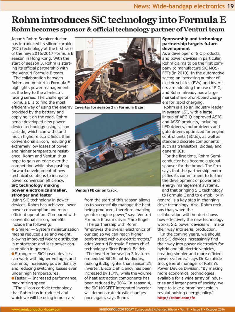
Japan’s Rohm Semiconductorhas introduced its silicon carbide(SiC) technology at the first raceof the new 2016/2017 Formula Eseason in Hong Kong. With thestart of season 3, Rohm is start-ing its official partnership withthe Venturi Formula E team. The collaboration between
Rohm and Venturi in Formula Ehighlights power managementas the key to the all-electric racing series. The challenge ofFormula E is to find the mostefficient way of using the energyprovided by the battery andapplying it on the road. Rohmhence developed new powerdevice technology using siliconcarbide, which can withstandmuch higher electric fields thanconventional silicon, resulting inextremely low losses of powerand higher temperature resist-ance. Rohm and Venturi thushope to gain an edge over thecompetition while also pushingforward development of new technical solutions to increasepower conversion efficiency. SiC technology makingpower electronics smaller,stronger and faster Using SiC technology in powerdevices, Rohm has achieved lowerpower consumption and more efficient operation. Compared withconventional silicon, benefitsinclude the following: ● Smaller — System miniaturizationmeans reduced size and weight,allowing improved weight distributionin motorsport and less power con-sumption in general. ●Stronger — SiC-based devicescan work with higher voltages andcurrents, increasing power densityand reducing switching losses evenunder high temperatures. ●Faster — Increased performance,maximizing speed. “The silicon carbide technology
that Rohm has introduced andwhich we will be using in our cars
from the start of this season allowsus to successfully manage the heatbeing produced, therefore enablinggreater engine power,” says VenturiFormula E team driver Maro Engel. The partnership with Rohm
“improves the overall electronics ofour car, so we can reach higher performance with our electric motors,”adds Venturi Formula E team chieftechnology officer Franck Baldet. The inverter for season 3 features
embedded SiC Schottky diodes,making it 2kg lighter than season 2’sinverter. Electric efficiency has beenincreased by 1.7%, while the volumeof heat extraction components hasbeen reduced by 30%. In season 4,the SiC MOSFET integrated inverterwill demonstrate drastic changesonce again, says Rohm.
Sponsorship and technologypartnership targets futuredevelopment As a developer of SiC productsand power devices in particular,Rohm claims to be the first com-pany to manufacture SiC MOS-FETs (in 2010). In the automotivesector, an increasing number ofelectric vehicles (EVs) and invert-ers are adopting the use of SiC,and Rohm already has a largemarket share of on-board charg-ers for rapid charging. Rohm is also an industry leader
in system LSI, with a largelineup of AEC-Q-approved ASICand ASSP products, includingLED drivers, motor drivers andgate drivers optimized for enginecontrol units (ECUs), as well asstandard discrete componentssuch as transistors, diodes, andgeneral ICs. For the first time, Rohm Semi-
conductor has become a globalsponsor for the brand. The firmsays that the partnership exem-plifies its commitment to furtherthe development of power andenergy management systems,and that bringing SiC technologyto Formula E and to e-mobility in
general is a key step in changingdrive technology. Also, Rohm reck-ons that, when the collaboration with Venturi showshow effectively the new technologyworks, SiC power devices will maketheir way into serial production. “In the coming years, we should
see SiC devices increasingly findtheir way into power electronics forhybrid and all-electric vehicles, creating simpler and more efficientpower systems,” says Dr KazuhideIno, general manager of Rohm’sPower Device Division. “By makingmore economical technologiesavailable for a wide array of indus-tries and larger parts of society, wehope to take a prominent role inrevolutionising energy policy.” http://rohm.com/fe
Inverter for season 3 in Formula E car.
Venturi FE car on track.
Rohm introduces SiC technology into Formula E Rohm becomes sponsor & official technology partner of Venturi team

News: Wide-bandgap electronics
semiconductorTODAY Compounds&AdvancedSilicon • Vol. 11 • Issue 8 • October 2016 www.semiconductor-today.com
20
Wolfspeed of Research TrianglePark, NC, USA — a Cree Companythat makes silicon carbide (SiC)power products including MOSFETs,Schottky diodes, and modules —has introduced what it claims is thefirst 1000V MOSFET, which enablesa reduction in overall system costwhile improving system efficiencyand decreasing system size. Specially optimized for fast chargingand industrial power supplies, thenew MOSFET enables a 30% reduc-tion in component count whileachieving more than a 3x increasein power density and a 33%increase in output power. “Supporting the widespread
implementation of off-board charg-ing stations, Wolfspeed’s technologyenables smaller, more efficientcharging systems that providehigher-power charging at loweroverall cost,” says chief technologyofficer John Palmour. “This marketrequires high efficiency and wideoutput voltage range to address thevarious electric vehicle (EV) batteryvoltages being introduced by auto-motive suppliers,” he adds.
“Wolfspeed’s new 1000V SiC MOSFET offers system designersultra-fast switching speeds with afraction of a silicon MOSFET’sswitching losses. The figure-of-meritdelivered by this device is beyondthe reach of any competing silicon-based MOSFET,” Palmour reckons. Designers can reduce component
count by moving from silicon-based,three-level topologies to simplertwo-level topologies made possibleby the SiC MOSFET’s 1000Vds rating.The increase in output power in areduced footprint is realized by theultra-low output capacitance (as lowas 60pF), which significantly lowersswitching losses. The new deviceenables operations at higherswitching frequencies, which shrinksthe size of the resonant tank elementsand decreases overall losses, reduc-ing heat-sink requirements, saysthe firm. Wolfspeed has determinedthese proof-points by constructinga 20kW full-bridge resonant LLCconverter and comparing it to amarket-leading 15kW silicon system. Wolfspeed offers a 20kW full-bridge
resonant LLC converter reference
design (part no. CRD-20DD09P-2).This fully assembled hardware setallows designers to quickly evaluatethe new 1000V SiC MOSFET anddemonstrate its faster switchingcapability, as well as the increasedsystem power density that thedevice enables, says the firm. The 1000V, 65mΩ MOSFET is
available in a through-hole 4L-TO247package (as part no. C3M0065100K)and is available for purchase atDigikey, Mouser and RichardsonRFPD. Wolfspeed plans to release another
1000V MOSFET in a 4L-TO247package at 120mΩ (C3M0120100K)in the coming weeks. This packagehas a Kelvin-source connection thatallows engineers to create designsthat maximize the benefits of SiC’ssuperior speed and efficiency. Surface-mount versions of these
devices (C3M0065100J andC3M0120100J) will be releasedlater this year. Like the 4L-TO247,these will include a Kelvin-sourcepin to help minimize gate-ringingand reduce system losses.www.wolfspeed.com/power/products
Wolfspeed launches first 1000V SiC MOSFET 65mΩMOSFET available in through-hole 4L-TO247 package, with 120mΩ imminent; surface-mount versions later this year
Qorvo Inc of Greensboro, NC andHillsboro, OR, USA has launchedtwo new power amplifiers (PAs)including what is claimed to be thefirst 500W, L-band PA internallymatched to 50Ω. The high-powerdevices are optimized for use indefense and civilian radar systems,with features designed to shortenand simplify system implementation. Built on Qorvo’s gallium nitride
(GaN) technology, the new QPD1003meets the performance needs ofhigh-power phased arrays such asactive electronic scanned array(AESA) radars, which operate in the1.2–1.4GHz frequency range.
These systems require PAs thatoperate at maximum efficiency,resulting in low heat generation indemanding environmental conditions.The QPD1003 addresses theserequirements through the use ofhighly efficient GaN on silicon carbide(SiC) technology. “This is the first and only compact,
internally matched and high-poweredL-band PA for AESA radar,” claimsRoger Hall, general manager ofHigh Performance Solutions at Qorvo. In addition, Qorvo has also
introduced a 450W S-band PA,designed for 3.1–3.5GHz S-bandradar systems. Both devices offer
advantages in size and ease ofimplementation over conventionalGaN transistors, it is claimed. Theyenable multiple frequency bands tobe covered by a single matcheddesign, reducing circuit footprintand overall complexity when usedin multi-kilowatt arrays. Addition-ally, reducing the amount of powerdissipation results in further systemoperational savings by reducing theneed to cool the system. The new PAs support pulsed and
linear operations, and are suppliedin an air-cavity package suited todefense & civilian radar applications. www.qorvo.com/defense
Qorvo launches compact GaN L- and S-band power amplifiers for advanced radar systems

News: Wide-bandgap electronics
www.semiconductor-today.com semiconductorTODAY Compounds&AdvancedSilicon • Vol. 11 • Issue 8 • October 2016
21
Qorvo Inc, a provider of core technologies and RF solutions formobile, infrastructure and aero-space/defense applications, haslaunched a family of gallium nitride(GaN) die transistors with thehigher-frequency performance andlow noise essential for advancedapplications in communications,radar and defense RF systems. The family includes six new GaN
transistors manufactured usingQorvo’s QGaN15 0.15μm GaN onsilicon carbide (SiC) process and itsassociated models. The QGaN15
process enables these transistors tooffer high-frequency operation ofup to 25GHz, supporting die-leveldesigns that deliver higher-frequency,cost-effective discrete technologyup through K-band applications. “The combination of higher-
performance GaN products, complementary models and dedicated applications engineeringsupport sets Qorvo apart,” claimsRoger Hall, general manager ofHigh Performance Solutions at Qorvo. Linear, non-linear and noise mod-
els, which enable rapid, accurate
performance testing and speedproduction readiness, are availablefrom partner Modelithics Inc ofTampa, FL, USA, which provides RF and microwave active and passivesimulation models for electronicdesign automation (EDA). Themodels offer features such as scaling of operating voltage, ambient temperature and self-heating effects, as well as intrinsicvoltage/current node access forwaveform optimization. www.modelithics.com/mvpQorvo.aspwww.qorvo.com
Qorvo launches new family of 0.15μμm GaN-on-SiC dietransistors, with new models available from Modelithics
Fabless high-temperature andextended-lifetime semiconductorfirm CISSOID of Mont-Saint-Guibert,Belgium is collaboratingwith Data Device Corp (DDC), whichdesigns and manufactures databus, motion control and solid-statepower controller products for aero-space, defense and industrial appli-cations, and with DDC subsidiaryBeta Transformer Technology Corp(BTTC), which produces military,commercial and space-level magnetic components, for thedevelopment of more compact andreliable silicon carbide (SiC) MOSFETintelligent power modules (IPM) foraerospace power converters andmotor control. BTTC will develop high-reliability
and high-temperature transformermodules, embedding both powerand pulse transformers, optimizedfor CISSOID’s HADES2 isolatedgate driver. This solution will beused in the SiC MOSFET intelligentpower modules developed by CISSOID, making them more com-pact and reliable. It will address SiC IPMs developed for high-power-density applications as well asIPMs in hermetically sealed pack-ages currently in development for
harsh environments (e.g. unpres-surized locations and/or extremetemperatures). The first transformers modules
are being developed, validated andqualified for temperature rangesfrom –55°C up to +225°C. Mag-netic cores and other transformermaterials have been selected tooffer stable behaviour and reliableoperation within this range. Thetransformers will provide isolationin excess of 2500Vdc and are opti-mized for very low parasitic capaci-tances in order to support highdV/dt, typically up to 50KV/µs(common with fast-switching SiCtransistors). These transformershave been optimized to work withthe HADES2 isolated gate driverchipset: the power transformer is
used inside a flyback DC–DC converter supplying both low- andhigh-side isolated gate driverswhile pulse transformers are trans-mitting PWM and Faults signals. “With DDC and BTTC, we found
the right partners to develop high-reliability and high-temperaturetransformer solutions for our SiCIPM and gate drivers. They bring toCISSOID their long experience indeveloping signal and power trans-formers for data transceivers andpower converters as well as theirhigh quality manufacturing facili-ties.” says CISSOID’s CEO DaveHutton. “This partnership showsCISSOID’s commitment to workwith partners to offer to its cus-tomers a complete ecosystem forthe development of high-tempera-ture system solutions,” he adds. “This first partnership with CISSOID
will trigger others as we see variouscollaboration opportunities betweenDDC and CISSOID, e.g. the development of high-temperaturemotor drive or power convertersolutions for aerospace, defenseand industrial applications,”believes Frank Bloomfield, VP Power Systems at DDC.www.cissoid.com
CISSOID and DDC cooperate on more compact and reliable SiC intelligent power modules
An IPM and a TRFO module.

News: Wide-bandgap electronics
semiconductorTODAY Compounds&AdvancedSilicon • Vol. 11 • Issue 8 • October 2016 www.semiconductor-today.com
22
The US Air Force Research Labora-tory (AFRL) and the Office of theSecretary of Defense (OSD) haveawarded Raytheon Company ofWaltham, MA, USA a $14.9m Title III contract to further enhanceits process for producing gallium nitride (GaN)-based semi-conductors. The new agreementfollows a previous GaN Title III contract, completed in 2013, andaims to increase the performance,yield and reliability of RaytheonGaN-based, wideband, monolithicmicrowave integrated circuits(MMICs) and circulator components. As GaN can efficiently amplify
high-power radio frequency signalsat microwave frequencies (enhanc-ing a system’s range and raid han-dling, while reducing size, weight,power and cost), it is used in abroad spectrum of military radars
and defense systems, including theUS Navy’s Air and Missile DefenseRadar (AMDR) and Next GenerationJammer (NGJ).
“We have only scratched the sur-face when it comes to harnessingthe game-changing power that gal-lium nitride technology can bring tomilitary applications,” believes ColinWhelan, VP of advanced technologyin Raytheon’s Integrated DefenseSystems (IDS) business unit. “Thiscontract will build on the 17-year,$200m+ investment Raytheon hasmade in maturing GaN,” he adds.“Over the next two years, we willfurther refine our GaN process topush the limits of radio frequencyperformance while maintaining orincreasing yield and reliability.” The first demonstrator of this
technology will be incorporated intoRaytheon Space and Airborne Systems’ Next Generation Jammerprogram, which is scheduled forlow-rate initial production in 2018. www.raytheon.com
AFRL and OSD award Raytheon $14.9m Title IIIcontract to enhance GaN process technology New contract to boost performance, yield and reliability of GaN-based, wideband MMICs
The US Missile Defense Agencyhas awarded Raytheon Companyof Waltham, MA, USA a contractmodification to develop a transi-tion to production process to incor-porate gallium nitride (GaN)components into existing andfuture AN/TPY-2 radars. This initialeffort will support the transitionfrom gallium arsenide (GaAs) toGaN technology, which would fur-ther modernize the ballistic missiledefense radar and drive down sys-tem obsolescence. As demonstrated in other
Raytheon-developed military radarapplications, GaN has the capabil-ity to enhance range, increasedetection and discrimination per-formance and lower productioncosts. Currently fielded AN/TPY-2 radars
use GaAs-based transmit/receive
modules to emit high-power radia-tion. Raytheon and the MDA arepursuing a retrofit approach toleverage GaN elements. “GaN components have signifi-
cant, proven advantages whencompared to the previous-genera-tion GaAs technology,” says DaveGulla, VP of Raytheon’s IntegratedDefense Systems Mission Systemsand Sensors business area."Through this effort, Raytheon will
develop a clear modernizationupgrade path for the AN/TPY-2radar, enabling the system to bet-ter defend people and criticalassets against ballistic missilethreats at home and abroad.” The AN/TPY-2 is a transportable
X-band radar that protects civiliansand infrastructure in the USA,deployed military personnel, andallied nations and security partnersfrom ballistic missile threats.According to recent Congressionaltestimony by the director of theMDA, the threat is growing aspotential adversaries acquire agreater number of ballistic mis-siles, increase their range, incor-porate countermeasures and makethem more complex, survivable,reliable and accurate. www.raytheon.com/capabilities/products/antpy2
Raytheon wins MDA contract modification to transition AN/TPY-2 radar production from GaAs to GaN
A GaN wafer undergoes fabricationprocess in Raytheon's foundry.
Raytheon’s AN/TPY-2 radar.

Distribution & Control Department
For sales, product & distributor information, please visit http://www.americas.fujielectric.com/componentsdistribution-control
or contact us: [email protected]
Compact! Ground Fault Protection Built in One Unit for Space Saving Designs
SameFootprint!MCCBs&ELCBsInterchangeablewithoutPanelModifications
18mm Per Pole Width(2P & 3P), IEC 35mm DIN Rail Mounting
Higher Capacity SCCR ⇒ 18kA@ 240VAC UL489
The New Generation of Low Voltage Earth Leakage Circuit Breakers
Fuji Electric Lambda SeriesNew, Compact, Powerful

News: Wide-bandgap electronics
semiconductorTODAY Compounds&AdvancedSilicon • Vol. 11 • Issue 8 • October 2016 www.semiconductor-today.com
24
Tokyo-based Mitsubishi ElectricCorp is expanding its lineup of gallium nitride high-electron-mobilitytransistors (GaN HEMTs) to includemodels operating at frequencies of13.75–14.5GHz with saturated out-put power of 100W (50.0dBm) and70W (48.3dBm) for use in satelliteearth stations utilizing the Ku-band(12–18GHz). Due to optimization ofthe transistor structure, the new100W GaN HEMT offers outputpower that is reckoned to beamong the highest available. Sample shipment will begin on 1 October (70W) 2016 and 1 Janu-ary 2017 (100W). Mitsubishi Electric says that
demand for satellite communicationsis increasing, especially in the Ku-band, which enables high-speedcommunication even under adverseconditions such as natural disastersand in areas where construction of
communication facilities is difficult.Deployment of transmitter equip-ment using higher-power GaN HEMTshas become more common inrecent years, particularly in high-speed applications such as satellitenews gathering. To meet this growing demand for
higher output power levels, Mitsubishi Electric is hence expand-ing its Ku-band GaN-HEMT lineup
with the 100W MGFK50G3745 modeland 70W MGFK48G3745 model(which both have 10.0dB linear gain).Mitsubishi Electric notes that, dueto the high output power, the needfor fewer parts contributes to theminiaturization of transmitterequipment in satellite earth stations. In addition, individual transmitter
components can be configuredindependently during manufacture,eliminating the need for on-siteconfiguration and shortening over-all development time. Finally, the existing MGFG5H1503
power amplifier can be used as adriver stage, leveraging the latter’slinearizer device to help reduce dis-tortion in power transmitters. Development of the new devices
was partially supported by Japan’sNew Energy and Industrial TechnologyDevelopment Organization (NEDO). www.MitsubishiElectric.com
Mitsubishi Electric expanding Ku-band GaN HEMTrange to 70W and 100W to shrink satellite earth stations
Mitsubishi Electric’s MGFK50G3745(left) and MGFK48G3745 (right).
At the 24th China Power SupplySociety Conference (CPSSC) inShanghai, China, co-organized bythe Power Institute of China andthe Shanghai Maritime University,in a three-hour seminar on 31 October, GaN Systems Inc ofOttawa, Ontario, Canada — a fablessdeveloper of gallium nitride (GaN)-based power switching semicon-ductors for power conversion andcontrol applications — presentedthe advanced technology session‘GaN E-HEMT Devices, Principles andApplications’ as part of a programthat introduces the most currentpower semiconductor devices. Global applications engineering
manager Di Chen will present theseminar to an audience consistingof several hundred researchers andengineers. Topics covered includenew wide-bandgap semiconductortechnology, and an in-depth analy-
sis of the structure, characteristicparameters, device selection andprotection of high-frequencyswitching devices used for efficientpower application problems. Theagenda for Chen’s workshop was asfollows: ● A basic introduction to GaN E-HEMT power transistors; ● GaN E-HEMT principles andpackage design; ● GaN E-HEMT technology andreliability; ● Driver & component selection; ● PCB layout and thermal consid-erations; and ● GaN E-HEMT applications. GaN Systems says that it
continues to invest heavily in supporting its Asian customers by providing in-country staff, technical support and resources.This is extended by providing practical technology workshops.
The firm says that it is bringingdesign knowledge to power systemengineers, enabling them to rapidlydevelop the most efficient andcompetitive products that leveragethe performance benefits of gallium nitride. “More and more customers in
China are developing leading-edgepower electronics,” notes CharlesBailley, director of GaN Systems’Asian operations. “Using GaN, theyhave been gaining a competitiveedge across the industrial, consumer, transportation, anddata-center server markets,” Bailley adds. “This workshop gives engineers the tools to understand and use GaN transistorsso they can meet their customers’power saving demands,” he concludes. www.cpss.org.cn www.gansystems.com
GaN Systems presents GaN HEMT workshop atChina Power Supply Society Conference

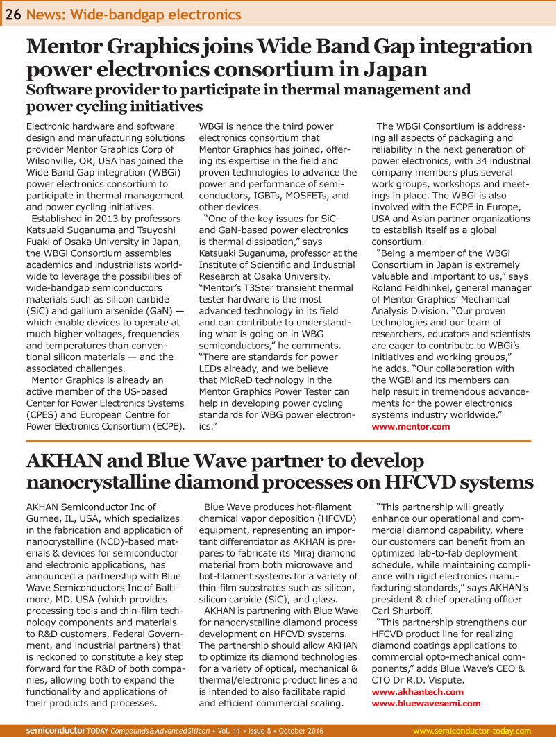
News: Wide-bandgap electronics
semiconductorTODAY Compounds&AdvancedSilicon • Vol. 11 • Issue 8 • October 2016 www.semiconductor-today.com
26
AKHAN Semiconductor Inc ofGurnee, IL, USA, which specializesin the fabrication and application ofnanocrystalline (NCD)-based mat-erials & devices for semiconductorand electronic applications, hasannounced a partnership with BlueWave Semiconductors Inc of Balti-more, MD, USA (which providesprocessing tools and thin-film tech-nology components and materialsto R&D customers, Federal Govern-ment, and industrial partners) thatis reckoned to constitute a key stepforward for the R&D of both compa-nies, allowing both to expand thefunctionality and applications oftheir products and processes.
Blue Wave produces hot-filamentchemical vapor deposition (HFCVD)equipment, representing an impor-tant differentiator as AKHAN is pre-pares to fabricate its Miraj diamondmaterial from both microwave andhot-filament systems for a variety ofthin-film substrates such as silicon,silicon carbide (SiC), and glass. AKHAN is partnering with Blue Wave
for nanocrystalline diamond processdevelopment on HFCVD systems.The partnership should allow AKHANto optimize its diamond technologiesfor a variety of optical, mechanical &thermal/electronic product lines andis intended to also facilitate rapidand efficient commercial scaling.
“This partnership will greatlyenhance our operational and com-mercial diamond capability, whereour customers can benefit from anoptimized lab-to-fab deploymentschedule, while maintaining compli-ance with rigid electronics manu-facturing standards,” says AKHAN’spresident & chief operating officerCarl Shurboff. “This partnership strengthens our
HFCVD product line for realizingdiamond coatings applications tocommercial opto-mechanical com-ponents,” adds Blue Wave’s CEO &CTO Dr R.D. Vispute. www.akhantech.com www.bluewavesemi.com
Electronic hardware and softwaredesign and manufacturing solutionsprovider Mentor Graphics Corp ofWilsonville, OR, USA has joined theWide Band Gap integration (WBGi)power electronics consortium toparticipate in thermal managementand power cycling initiatives. Established in 2013 by professors
Katsuaki Suganuma and TsuyoshiFuaki of Osaka University in Japan,the WBGi Consortium assemblesacademics and industrialists world-wide to leverage the possibilities ofwide-bandgap semiconductorsmaterials such as silicon carbide(SiC) and gallium arsenide (GaN) —which enable devices to operate atmuch higher voltages, frequenciesand temperatures than conven-tional silicon materials — and theassociated challenges. Mentor Graphics is already an
active member of the US-basedCenter for Power Electronics Systems(CPES) and European Centre forPower Electronics Consortium (ECPE).
WBGi is hence the third power electronics consortium that Mentor Graphics has joined, offer-ing its expertise in the field andproven technologies to advance thepower and performance of semi-conductors, IGBTs, MOSFETs, andother devices. “One of the key issues for SiC-
and GaN-based power electronics is thermal dissipation,” says Katsuaki Suganuma, professor at theInstitute of Scientific and IndustrialResearch at Osaka University.“Mentor’s T3Ster transient thermaltester hardware is the mostadvanced technology in its field and can contribute to understand-ing what is going on in WBG semiconductors,” he comments.“There are standards for powerLEDs already, and we believe that MicReD technology in the Mentor Graphics Power Tester canhelp in developing power cyclingstandards for WBG power electron-ics.”
The WBGi Consortium is address-ing all aspects of packaging andreliability in the next generation ofpower electronics, with 34 industrialcompany members plus severalwork groups, workshops and meet-ings in place. The WBGi is alsoinvolved with the ECPE in Europe,USA and Asian partner organizationsto establish itself as a global consortium. “Being a member of the WBGi
Consortium in Japan is extremelyvaluable and important to us,” saysRoland Feldhinkel, general managerof Mentor Graphics’ MechanicalAnalysis Division. “Our proventechnologies and our team ofresearchers, educators and scientistsare eager to contribute to WBGi’sinitiatives and working groups,” he adds. “Our collaboration withthe WGBi and its members can help result in tremendous advance-ments for the power electronicssystems industry worldwide.” www.mentor.com
Mentor Graphics joins Wide Band Gap integrationpower electronics consortium in Japan Software provider to participate in thermal management and power cycling initiatives
AKHAN and Blue Wave partner to developnanocrystalline diamond processes on HFCVD systems

Keysight Technologies Inc of Santa Rosa, CA, USA (which pro-vides electronic measurementinstruments, systems and relatedsoftware used in the design, devel-opment, manufacture, installation,deployment and operation of elec-tronic equipment) has collaboratedwith Virginia Diodes Inc (VDI,which makes test & measurementequipment for millimeter-wave andterahertz applications) to create a1.5THz measurement solution forChalmers University of Technologyin Gothenburg, Sweden. Already upand running in Chalmers’ nationallaboratory for terahertz characteri-zation, the industry-first solutionprovides network and spectrumanalysis capabilities for research onnew materials, devices and circuits
for applications at micro-, millimeter-and sub-millimeter-wave frequencies. Chalmers’ researchers are work-
ing in the terahertz gap betweenradio waves and infrared light. The measurement equipment fromKeysight provides new capabilitiesthat are enhancing their work withfree-space, on-wafer and waveguidemeasurements in the terahertz gap.
The system is built around theKeysight’s PNA-X microwave networkanalyzer, which covers 10MHz to67GHz and reaches 1.5THz withexternal extension modules fromVDI. Achieving an insightful under-standing of device performance andbehavior requires network andspectrum measurements, saysKeysight, which claims that thePNA family is the first to provideintegrated spectrum analysis capa-bility that reaches into the terahertzrange. The ability to access bothcapabilities in a single test setup —and make multiple measurementsthrough one set of connections —saves time and enhances insight. www.keysight.com/find/1.5THZ www.chalmers.se/en www.vadiodes.com
Chalmers chooses Keysight and Virginia Diodes to createfirst system for network & spectrum analysis up to 1.5THz Capabilities enhance free-space, on-wafer & waveguide measurements ofmaterials, devices and circuits at terahertz frequencies
News: Materials and processing equipment
www.semiconductor-today.com semiconductorTODAY Compounds&AdvancedSilicon • Vol. 11 • Issue 8 • October 2016
27
A Keysight PNA network analyzer
Test, measurement and monitoringequipment supplier Tektronix Inc ofBeaverton, OR, USA has introducedthe Keithley S540 Power Semicon-ductor Test System, a fully auto-mated, 48-pin parametric test systemfor wafer-level testing of power semi-conductor devices and structuresup to 3kV. Optimized for compoundpower semiconductor materialsincluding silicon carbide (SiC) andgallium nitride (GaN), the S540 canperform all high-voltage, low-voltageand capacitance tests in a singleprobe touch-down. As demand for power semiconduc-
tor devices continues to increaseand as SiC and GaN become morecommercialized, manufacturers areadopting wafer-level testing in theirproduction processes to optimizeyields and improve profitability, saysTektronix. For these applications,the S540 lowers cost of ownershipby minimizing test time, test set-up
time and floor space while achiev-ing lab-grade high-voltage meas-urement performance, it adds. “Many fabs are using custom-built,
hybrid test systems for power semi-conductor testing that require manually changing test setups whenmoving from low-voltage to high-voltage tests,” says Keithley productline general manager Mike Flaherty.“As you might expect, this addsprocess steps and slows production,”he adds. “In contrast, the S540 is acomplete, fully integrated solutionwell suited for production environ-ments where numerous devicesmust be tested quickly.” To deliver production-level per-
formance, the S540 can performparametric measurements on up to48 pins without changing cables orprobe card infrastructure. It canalso perform transistor capacitancemeasurements such as Ciss, Coss,and Crss up to 3kV, again without
manual reconfiguration of test pins.Further boosting test output, theS540 offers sub-pA measurementperformance and can perform fullyautomated, high-voltage leakagecurrent tests in <1s. As a standard commercial product,
the S540 offers fully traceable system specifications, safety com-pliance, diagnostics, and worldwideservice and support, features thatare often missing in home-built orcustom systems. The S540 drawson Keithley’s 30+ years of semicon-ductor parametric testing expertise,and safely and seamlessly integratessemiconductor test instrumentationwith both low- and high-voltageswitching matrices, cabling, probe card adapters, prober driversand test software. The Keithley S540 is available to
order now, for delivery from March. www.tek.com/keithley-s540-parametric-test-system
Tektronix launches Keithley S540 power semiconductortest system targeting SiC and GaN devices up to 3kV

News: Materials and processing equipment
semiconductorTODAY Compounds&AdvancedSilicon • Vol. 11 • Issue 8 • October 2016 www.semiconductor-today.com
28
For third-quarter 2016, AXT Inc ofFremont, CA, USA — which makesgallium arsenide (GaAs), indiumphosphide (InP) and germanium(Ge) substrates and raw materials— has reported revenue of $21.9m(above the expected $20.5–21.5m).This is up 7% on $20.5m last quarterand up 19% on $18.4m a year ago,driven by stronger-than-expecteddemand for GaAs.Of total revenue, 66% came from
Asia Pacific, 23% from Europe, and11% from North America. Only onecustomer generated over 10% ofrevenue, and the top five generated38% (down from 42% last quarter),reflecting the ongoing diversificationof both products and customers. “The global build out of fiber-
optical connections continue to bethe leading driver of our InP sales,”says CEO Morris Young. “Fiber-optictechnology is helping to enable thefruition of applications such as cloudcomputing, the Internet-of-Thingsand video streaming. Worldwidefiber deployment has 100 millionconnections in 2015 and is expected tocontinue to grow for the long term.”However, GPON and EPON marketsin China are taking a pause torebalance following two years ofstrong growth, notes Young. “Thissoftness caused a modest decline inindium phosphide sales in Q3.” “Our raw material business remain
under pricing pressure,” says Young.Revenue from AXT’s seven consoli-dated joint ventures was down$581,000. “But we are seeing pricestart to stabilize and in some casesimprove,” he notes. “Gallium priceduring the quarter seems to havestabilized and has ticked up a littlebit, as has germanium pricing. Thiscould lead to a more favorable pricingenvironment in quarters to come.” Gross margin has risen further, from
25.1% a year ago and 29.4% lastquarter to 34.6% (the highest sinceQ1/2012), due to higher productionvolume, a favorable product mix
(including InP substrate and othermaterials with high-end applications)and good progress in manufacturingefficiencies and yield improvements(especially in crystal growth). Operating expenses have been cut
further, from $5.3m a year ago and$5.1m last quarter to $4.9m.“Through the implementation of anumber of programs, we areachieving improved deals for bothingots and wafer processing,” saysYoung. “The benefit of these in-progress and other cost-reductionmeasures are becoming increasinglyvisible in our financial results.” Net income has recovered further,
from breakeven a year ago and$1.2m ($0.03 per diluted share)last quarter to $2.2m ($0.07 perdiluted share, above the expected$0.03-0.05 per diluted share).Depreciation and amortization were
steady at $1.2m. Capital expenditure(CapEx) was $0.5m (halved from$1m last quarter). After generatingpositive cash flow during Q3, cash,cash equivalents and investmentsrose by $2.4m from $45m to $47.3m. For Q4/2016, revenue is expected
to fall to $18.5–19.5m. InP revenuewill rebound slightly, as increasinggrowth for fiber-to-the-home (FTTH)deployment and data-center con-nectivity will offset the continuingGPON- and EPON-related inventoryadjustment in China. However, thiswill be outweighed by declines of$0.15m in germanium, $1m in GaAs(due mainly to temporary inventoryadjustments by two major customersfor semi-insulating GaAs followingan unusually strong Q3, plus aslight $100,000–150,000 decline insemiconducting GaAs), and $1.5min raw materials (following a strongQ3, which had included a sizabledelivery to Japan of about 10 tonsof gallium). Net income should be$0.02–0.04 per diluted share. “In spite of these near-term factors
that are expected in a down quarterin Q4, we do not see any fundamen-
tal changes in our key markets,” noteschief financial officer Gary Fischer. “Sales of semi-insulating GaAs has
reached a relative stable level thatprovides a healthy base of profitablerevenue,” says Young. “Also, we areworking with customers on certaininvestigations of new applicationsfor the material that could providefuture upside potential,” he adds.“In the semiconducting GaAs market,we continue to participate selectivelyin high-end LED applications suchas backlighting, signage and auto-motive,” continues Young. “Whilethe LED market remains highlycompetitive and fragmented, we areseeing relative stable demand thatwe expect to continue into 2017.” “Long term, we are closely watching
the continued market developmentof VCSELs for 3D sensing applications,such as gaming, mobile phones,smart TVs, high-speed communica-tions and high-power material pro-cessing. 3D sensing requires deviceswith relative high-precision func-tionality and consistent reliability,”Young notes. This translates into theneed for very low defect densities,i.e. very low etch-pit density (EPD).“Our VGF technology and propri-etary processes allow us to offerindustry-leading specifications thatcreates a significant competitiveadvantage for high-end VCSELapplications. This application couldprovide an attractive opportunityfor our business if it is adopted intohigh-end smartphones, which couldtotal 500–600 million units per year.” “We are focusing our resources on
strategic product applications inInP, GaAs and Ge substrates that areshowing promising market trends,”Young says. “InP is a growth driverfor our business in fiscal year 2017and beyond, and we expect that GaAswill continue to provide a stablerevenue base with upside potentialfrom VCSELs and other investiga-tional applications,” adds Fischer. www.axt.com
AXT’s revenue grows 7% in third-quarter 2016, driven by stronger-than-expected demand for GaAs InP inventory corrections in China suppress growth

News: Materials and processing equipment
www.semiconductor-today.com semiconductorTODAY Compounds&AdvancedSilicon • Vol. 11 • Issue 8 • October 2016
29
UK-based process equipmentmaker Oxford Instruments hasannounced the development andlaunch of a silicon carbide (SiC) viaplasma etch process using itsPlasmaPro100 Polaris etch system. SiC is becoming an increasingly
important material, particularly forgallium nitride (GaN) RF devicesusing SiC as a substrate. A smoothvia etch through the SiC is essentialto enable these devices. OxfordInstruments says that it has developed a solution for etchinghigh-quality SiC vias efficiently.Combined with a low-damage GaNetch within the same hardware, thePlasmaPro100 Polaris offers what isclaimed to be a unique capabilityfor GaN-based RF device plasmaetch processing requirements. The new technology offers several
process capabilities suited to theSiC via application:
● high SiC etch rate, enablingmaximum throughput; ● smooth sidewalls for problem-freepost-etch metallization; ● high selectivity to underlyingGaN layers, giving a smooth, low-damage stop onto the GaNdevice layers; ● clamping of sapphire carriersusing Oxford Instruments’ patented
Electrostatic Clamp technology,ensuring sample temperature control and maximum yield; ● capability of etching SiC and GaNin the same tool through advancedplasma source technology; and ● high utilization provided by long mean time between cleans(MTBC). “Our applications specialists have
spent significant time developingthis SiC via etch process on thePlasmaPro100 Polaris etch system,enabling high selectivity andthroughput, amongst other benefits,” says Dr Mark Dineen,optoelectronics product manager atOxford Instruments Plasma Tech-nology (OIPT). “These benefits will enable our customers to etchboth SiC and GaN in the same toolthrough advanced plasma sourcetechnology,” he adds. www.oxford-instruments.com/plasma
Oxford Instruments develops SiC via etch for GaN-on-SiC RF device manufacture
SEM showing smooth via etchthrough SiC.
News: Materials and processing equipment
semiconductorTODAY Compounds&AdvancedSilicon • Vol. 11 • Issue 8 • October 2016 www.semiconductor-today.com
30
SENTECH Instruments GmbH ofBerlin, Germany says that theInstitute for Microelectronics andMicrosystems (CNR-IMM) in Catania— which is part of the Physics andMatter Technologies Department(DSFTM) of the National ResearchCouncil of Italy (CNR) — is using anSI PEALD LL plasma-enhancedatomic layer deposition tool with an 8-inch wafer configuration toinvestigate the integration of novelhigh-k gate dielectrics and passi-vating layers on devices based ongallium nitride (GaN) and otherwide-bandgap semiconductors. SENTECH says that its proprietary
true remote CCP (capacitively coupled plasma) source is especiallysuited to such low-temperature andno-damage applications. The specialdesign of the plasma source allowsonly radicals to reach the wafersurface, whereas high-energy photons and ions are completelyblocked. In conjunction, IMM and SENTECH
have signed a joint development
agreement (JDA) with the aim ofthe developing and characterizinglaminated layers. The use of alter-native high-k materials enables theshrinking of devices while main-taining their capacitance andreducing the leakage current den-sity. In particular, the growth ofAl2O3-HfO2 laminated layers isamong the most often used combi-nations for such applications. “The SENTECH SI PEALD LL reac-
tor is a high-performance and flexi-ble system, allowing the productionof several high-quality dielectricthin films, whose physical proper-ties can be tailored upon changingtheir chemical composition,” saysDr Raffaella Lo Nigro, who is thescientist in charge of the SI PEALDLL tool and of cooperation withSENTECH. Nigro has wide-rangingexpertise in the synthesis of binaryand complex thin films by chemicalvapor deposition (CVD) methodsfor several microelectronic appli-cations. “Possible applications ofthis activity are related not only to
the integration of novel gatedielectrics and passivating layerson wide-bandgap semiconductorsbut also for RF devices based ongraphene,” he adds. The results of this work have
already been published in scientificpapers (Raffaella Lo Nigro,Emanuela Schilirò, Giuseppe Greco,Patrick Fiorenza and Fabrizio Roc-caforte, Thin Solid Films, vol601,2016, p68–72). NanolaminatedAl2O3-HfO2 and Al2O3/HfO2 bilayerthin films have been grown by PEALDon silicon substrates. Morphological,crystalline and electrical propertiesof the layer stacks were analyzedafter low-temperature depositionand high thermal treatment. The highly stable deposition of singlefilms and multi-layer laminatesusing SENTECH PEALD togetherwith very good uniformity of thedeposition process over the wholewafer are essential prerequisites forapplications such as designing newhigh-k dielectrics, says the firm. www.sentech.de
Deposition and process equipmentmaker Veeco Instruments Inc ofPlainview, NY, USA has announcedadditional cost-reduction initiativesafter deciding to significantlyreduce future investments in itsatomic layer deposition (ALD) tech-nology development, reflecting itsongoing focus to balance technol-ogy investments with the potentialfor associated revenue realization. ALD cost-reduction activities are
expected to be completed by theend of 2016 and are in addition tothe restructuring plans (announcedon 1 August), which targeted $20min annualized savings (starting infirst-quarter 2017). In total, these
initiatives are now expected to gen-erate $30m in annualized savings. “While we have continued to make
progress with our ALD technologydevelopment for advanced semicon-ductor applications, the expectedtiming for revenue realization hasbeen delayed,” says chairman & CEOJohn R. Peeler. “Consequently, wehave made the difficult decision tolower investments in our ALD pro-gram,” he adds. “We plan to retainthe intellectual property and tech-nology capabilities and continue toassess future market opportunities.” In third-quarter 2016, Veeco
expects to record total assetimpairment and restructuring
charges of $56–62m ($1.44–1.59on a per-share basis). Of thesecharges, the vast majority are non-cash, relating to an intangible ALDasset impairment, while about $2mare cash restructuring charges. Q3 revenue guidance update Overall LED industry conditions anddemand for Veeco’s products havecontinued to improve, says thefirm. As a result, revenue for third-quarter 2016 is expected tobe at the high end of the guidancerange of $70–85m (announced on1 August). Veeco plans to issuethird-quarter 2016 financial resultson 1 November. www.veeco.com
Veeco reducing investment in ALD technologyafter revenue realization delayed Q3 revenue expected to be at high end of $70–85m guidance range
CNR-IMM Italy using SENTECH PEALD system fornew high-k materials on wide-bandgap devices

News: Materials and processing equipment
www.semiconductor-today.com semiconductorTODAY Compounds&AdvancedSilicon • Vol. 11 • Issue 8 • October 2016
31
Optoelectronics manufacturerChangelight Co Ltd of Xiamen,Fujian Province, China has orderedadditional Veeco TurboDisc K475iarsenic phosphide (As/P) metal-organic chemical vapor deposition(MOCVD) system capability to boostproduction of red, orange, yellow(R/O/Y) LEDs. Changelight qualifiedand put into production Veeco’spremiere K475i system in February. “Our first K475i system has exceeded
our expectations in terms of loweringmanufacturing costs, driving excep-tional uniformity and producingunmatched yield and brightness,”says Shuangxiang Zhang, generalmanager of Yangzhou Changelight.“Adding this capability will enableus to meet existing demand for
red, orange, yellow LEDs, as well asposition ourselves to capitalize on theemerging As/P photonics market.” Introduced in February, the K475i
system incorporates proprietaryTurboDisc and Uniform FlowFlangeMOCVD technologies and enablesusers to reduce LED cost per wafer byup to 20% compared with alternativesystems, it is reckoned, via higherproductivity, best-in-class yieldsand reduced operating expenses. “Changelight’s quick adoption of
Veeco’s K475i technology is a tes-tament of its production-provenfunctionality,” says Veeco’s president William J. Miller Ph.D.“Changelight will benefit from superior uniformity and repeatability,lowering their cost of ownership.”
Veeco says that its proprietaryUniform FlowFlange technologyproduces films with very high uni-formity and improved within-waferand wafer-to-wafer repeatability,resulting in what is reckoned to bethe industry’s lowest cost of owner-ship. The patented technology issaid to provide ease-of-tuning forfast process optimization and fasttool recovery time after mainte-nance, enabling the highest pro-ductivity for applications such aslighting, display, solar, edge-emitterlaser diodes, vertical-cavity surface-emitting lasers (VCSELs) and hetero-junction bipolar transistors (HBTs). www.changelight.com.cn/enwww.veeco.com/products/turbodisc-k475i-asp-mocvd-system
On 21 October, deposition equipmentmaker Aixtron SE of Herzogenrath,near Aachen, Germany was told thatGermany’s Federal Ministry of Eco-nomics and Energy (Bundesminis-terium für Wirtschaft und Energie,or BMWi) had withdrawn the Clearance Certificate issued on 8 September to China’s FujianGrand Chip Investment Fund LP (an indirect shareholder of Germansubsidiary Grand Chip InvestmentGmbH) regarding its proposed offerto acquire Aixtron, and reopenedreview proceedings. In May, Aixtron agreed to a takeover
by Grand Chip Investment GmbH.Fujian Grand Chip Investment Fund LPis held 51% by Chinese businessmanand private investor Zhendong Liuand 49% by Xiamen Bohao Invest-ment Ltd (which is indirectly con-trolled by private investors ZhongyaoWang and Wanming Huang). Fujian Grand Chip (FGC) hence
announced a voluntary public takeoveroffer to acquire all of Aixtron SE’soutstanding ordinary shares andAmerican depository shares (ADS).Shareholders were offered €6 perordinary share, valuing Aixtron’s
equity (including net cash) at about€670m and reflecting a 50.7% pre-mium to the three-month volumeweighted average share price priorto the announcement. Aixtron and FGC said the trans-
action aimed to support Aixtron’slong-term R&D activities to bringnew products and technologies tomarket, support the execution ofthe firm’s current strategy andtechnology roadmaps, and improveits ability to compete and grow inChina. Specifically, R&D competencyand Aixtron’s existing technologywere to be maintained at the existingtechnology centers. FGC also agreedthat Aixtron would further strengthenits technology and IP portfolio,which would remain vested withAixtron, including in Germany. In addition, Aixtron’s existing globalset up would be maintained andexpanded at its three technologyhubs in Herzogenrath (Germany),Cambridge (UK) and Sunnyvale, CA(USA), possibly supplemented byfurther international technology hubs.The legal domicile and headquarterswould remain in Herzogenrath.Martin Goetzeler was to remain CEO
of Aixtron and Dr Bernd Schultechief operating officer, with FGCnominating four candidates to thesix-member Supervisory Board. However, according to the BMWi,
information available to the GermanFederal Government indicated thatAixtron’s know-how also comprisessecurity-related technologies (inparticular for the defense sector)that could be revealed through theacquisition. According to the New York Times,
concerns have arisen regarding pos-sible links between Chinese stateinvestment in both FGC and San’anOptoelectronics Co Ltd (China’slargest LED maker). Berlin-basedthink-tank Mercator Institute saysthat Xiamen Bohao is a local gov-ernment investment fund that haslinks to San’an. In early 2016,San’an failed to qualify Aixtron’snew AIX R6 metal-organic chemicalvapor deposition (MOCVD) system,leading to the truncation of a largemulti-system order. This prompteda drop in Aixtron’s share price, priorto the deal with FGC. www.grandchip-aixtron.comwww.aixtron.com
Changelight adds capacity with Veeco K475i technology
Clearance withdrawn for sale of Aixtron to Grand ChipReview proceedings to be reopened

News: Materials and processing equipment
semiconductorTODAY Compounds&AdvancedSilicon • Vol. 11 • Issue 8 • October 2016 www.semiconductor-today.com
32
SPTS Technologies Ltd of Newport,Wales, UK (an Orbotech companythat manufactures etch, PVD andCVD wafer processing solutions forthe MEMS, advanced packaging,LED, high-speed RF on GaAs, andpower management device markets)has recently won four businessawards. At this year’s Best Factory Awards
organized by Cranfield School ofManagement, SPTS was presentedwith the Innovation Award and theExport Award. Having met thequalification criteria set by thejudging panel as well as a comprehensive factory audit, the Innovation Award recognizesSPTS for its level of innovationthroughout the company. TheExport Award notes the firm’s proportion of export sales of 95%.The judges noted the multi-dimen-sional aspects of innovation atSPTS, which enables the firm toremain at the forefront of technicaladvances in semiconductor process
technologies and to bring industry-leading products to its global markets. The judges also pointedto SPTS’ lean manufacturingprocesses and commitment to continuous improvement whichprovides improved operational efficiencies and annual cost savingsto the business. Also, at the ceremony for the
Insider 2016 Made in Wales Awardsat Cardiff City Hall (which celebratethe best in manufacturing, designand product development fromacross Wales), SPTS received theApprenticeship Scheme of the YearAward and was crowned the Large Manufacturer of the Year. The Made in Wales Awards also recognized SPTS Technologies’export salesby short list-ing it in theExporter ofthe YearAward category.
“It’s the commitment to continuousimprovement across the entireorganization that has allowed us togrow our business, both operationallyand profitably, year on year,” saysKevin Crofton, president of SPTSand corporate VP at Orbotech. “The Best Factory Awards judgingprocess was on par with some ofour most demanding customeraudits, and we are extremely proudto be recognized for manufacturingexcellence by the team of assessorsfrom Cranfield School of Manage-ment, the IEE and other independ-ent institutions,” he adds. The Insider Made in Wales
Apprenticeship Scheme of the YearAward “recognizes our commitmentto identifying and attracting youngpeople to our industry and company,”Crofton continues. “Our apprentice-ship program is one element ofmany programs that helps SPTSensure our future with a skilled talent pool.” www.spts.com
UK-based Oxford Instruments hasannounced its 2016 technical work-shops in India (22–23 November).Now in their fifth year (followingprevious workshops in Bangalore,Mumbai, Chennai, Kolkata andMohali), this year’s event ‘Bringingthe Nanoworld Together 2016’returns to the Indian Institute ofScience (IISc) Bangalore, the location of the first workshop. Showcasing nanotechnology tools
and their use in multiple appli-cations, the two-day seminar willcomprise over 24 talks from Indianand international speakers, as wellas Oxford Instruments scientists.There will also be technical postersessions, providing participantswith the chance to discuss researchin detail, as well as networking
opportunities. The event is organised in two
parallel sessions: ● Sessions on Nanoscale PlasmaProcessing cover multiple areasincluding the latest advances inetch and deposition technologies,graphene and 2D materials andtheir applications, ion beam technologies, and emerging applications including atomic-scaleprocessing, quantum and BioMEMS. ● Sessions on NanoScience Cryofreeresearch tools comprise an intro-duction to nanotechnology, innova-tions in ultra-low-temperatureresearch, sensing individual pho-tons with atomic membranes, thelatest developments in cryogen-free high-magnetic-field and low-temperature sample environments
for neutron scattering, the appli-cation relevance of key Cryofreetool innovations, and more. “We intend these educational
seminars to improve participants’knowledge, and to keep themabreast of the latest technologicaladvances in these research areas,”says Frazer Anderson, strategicmarketing & development directorfor Oxford Instruments PlasmaTechnology (OIPT). “The workshopsprovide ample opportunities fornetworking, debate and discussionaround the rapidly evolving nanotechnology world.” The seminar is free to attend
but prior booking is essential, asprevious seminars have seen over300 registrations. www.oxford-instruments.com/btnt
Oxford Instruments’ 2016 technical workshopsreturn to IISc Bangalore
SPTS wins two Best Factory Awards and two Insider Made in Wales Awards
The ExportAward notes thefirm’s proportionof export sales of 95%

E: [email protected]: +44(0)1389 875444WWW.LOGITECH.UK.COM DISCOVER PROGRESS
THE NEW PM6: PRECISION LAPPING & POLISHING SYSTEM
*Compared to Logitech PM5 System
PRODUCE SUPERIOR SPECIMENS EVERY PROCESS WITH
!"Process wafers up to 4”/100mm diameter
!"#$%&'"()''*("+,"-)"&+".//0)1"2",%(&'0"$%))345"0%&'("6"3470'%('*"899
!":-&+1%&37"#$%&'""";$%&4'(("<+4&0+$
!"9'%$"&31'"*%&%"" " """7+$$'7&3+4"6",''*"=%7>""""?3%"@$-'&++&A
!""B470'%('*"%77-0%7C"D3&A")+$3(A345"0%&'("improved 30% - 50%*
EA'"#8F"#0'73(3+4"G%))345"6"#+$3(A345"(C(&'1"*'$3?'0("'4A%47'")0+7'((")'0,+01%47'"&A0+-5A"%"0%45'"+,"34&-3&3='"+)'0%&+0"7+4&0+$(H"(-7A"%("7+1=34'*"$%))345"6")+$3(A345"+)&3+4("%4*"@$-'&++&A"'4%=$'*",'%&-0'(I"EA3("='47A2&+)"(+$-&3+4"%$$+D(",+0"'%(C")0+7'(("0')'%&%=3$3&CH",%(&'0")0+7'(('("%4*"A35A"$'?'$("+,"-('0"7+4&0+$I
C
M
Y
CM
MY
CY
CMY
K
full page.pdf 1 8/19/2016 2:43:28 PM

News: Materials and processing equipment
semiconductorTODAY Compounds&AdvancedSilicon • Vol. 11 • Issue 8 • October 2016 www.semiconductor-today.com
34
Jing Zhang, an engineering facultymember at Rochester Institute ofTechnology, has received a$305,000 grant from the USNational Science Foundation (NSF)to acquire an inductively coupledplasma reactive-ion etching (ICP-RIE)system for photonic, electronic andbio-device fabrication. The systemstrengthens RIT’s fabrication capability in its Semiconductor &Microsystems Fabrication Laboratoryto support new and existing multi-disciplinary research in science andengineering, to enable educationalcurriculum development, and beused for workforce developmentand training activities led by RIT’sengineering college. “There is no equipment like this close
by so there was a huge need, and itwill help with collaborations we havewith other university and corporateresearchers,” says Zhang, the KateGleason Endowed Assistant Professorin the electrical and microelectronicengineering department in RIT’sKate Gleason College of Engineering.
“The instrument is essential toenable research and education onIII-nitride-based light-emittingdiodes and lasers, and other semi-conductor devices. We are studyingevery aspect of this material, fromunderstanding the physics to therealization of novel devices. Thisequipment will help with thatprocess,” says Zhang, who has beenat RIT since 2014 and is part of agrowing group of semiconductormaterials and photonics deviceresearchers at the university. She has expertise in ultraviolet andvisible LEDs, and in developingsemiconductors for optoelectronicand electronic devices. With the
emphasis onworkforcedevelopmentin photonics,having thenew equip-ment alsoprovides akey educa-
tional opportunity for training. RIT’smicroelectronic engineering depart-ment provides short courses insemiconductor fabrication for areahigh school and community collegeteachers and for regional companyemployees looking to advanceknowledge in this area. In the past year, RIT also acquired
a metal-organic vapor-phase epitaxy(MOVPE) system for the growth ofIII-V materials. The tool givesresearchers the ability to fabricateoptical and electronic devices andwill be a key learning and trainingresource. This capability was oncean outsourced to research labora-tory partners such as NASA. Now,the in-house functionality providedby this equipment, combined withthe ICP-RIE system, is available toRIT researchers as well as theregional Rochester photonics community, including partners inthe consortium AIM Photonics(American Institute for Manufac-turing Photonics), Zhang says. www.smfl.rit.edu
Plasma etch and deposition equip-ment maker CORIAL S.A.S. ofBernin, France has announced theavailability of hard materials deepetch processes using a new genera-tion of 200mm ICP-RIE (inductivelycoupled plasma reactive-ion etch)equipment. “With this new generation of
200mm ICP-RIE equipment, notonly new customers will benefitfrom enlarged process capabilitiestowards deep etching of hard mat-erials, but contracted customerswould also be able to get access tothis technology through systemupgrades,” notes marketing man-ager Elsa Bernard-Moulin. Deep etching of silicon, achieved
via Bosch or cryogenic microfabri-
cation technologies, is routinelyused for micro-electro-mechanicalsystem (MEMS) manufacturing tocreate micro-structures with highdepth and high aspect ratios. Besides silicon, a number of hard
materials — typically glass, quartz,silicon carbide (SiC) and lithiumtantalate — have attracted interestin the MEMS and packaging indus-tries, either due to their uniqueproperties or to reduce manufac-turing costs. One of the main challenges to the adoption of thesehard materials is the ability to create deep structures using deep reactive-ion etching (DRIE)processes. In recent months, CORIAL’s R&D
team has developed appropriate
processes and equipment for hardmaterials DRIE. “We have upgradedour ICP-RIE equipment with fea-tures such as high-power (2kW)ICP source, high-power (1kW) RF bias supply, retractable quartzliner to protect the reactor walls,higher-capacity turbo pump, oroptimized system for wafer cooling,”says Bernard-Moulin. “These system upgrades, combined withthe experience of our applicationspecialists, have enabled us todevelop hard materials DRIEprocesses with high etch rate,superior profile control, smoothsurface, excellent selectivity andanisotropic profile for more than100µm depth”. www.corial.net
CORIAL announces hard materials DRIE processesfor MEMS manufacturing
RIT awarded NSF grant for ICP-RIE etch system forphotonics and nanoelectronic device R&D
The instrumentis essential toenable researchand educationon III-nitride-based light-emitting diodesand lasers

The Mark of
Precision.Purity.
Performance.
SeMI-GaS® IS Powered By
For over 35 years, SEMI-GAS® has been the
semiconductor industry’s go-to brand for
premier, production-ready, ultra high purity
gas delivery systems. Today, Tier 1 leaders and
high-tech innovators all over the world look to
SEMI-GAS® for proven solutions that uphold
their rigorous application demands.
When it comes to ultra high purity gas delivery systems, look for the mark of excellence.
Learn more at www.semi-gas.com/mark
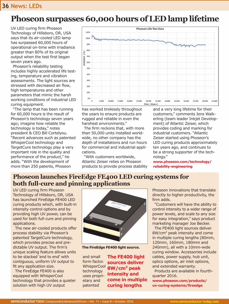
News: LEDs
semiconductorTODAY Compounds&AdvancedSilicon • Vol. 11 • Issue 8 • October 2016 www.semiconductor-today.com
36
UV LED curing firm Phoseon Technology of Hillsboro, OR, USAsays that its air-cooled LED lamphas surpassed 60,000 hours ofoperational on-time with irradiancegreater than 80% of its originaloutput when the test first beganseven years ago. Phoseon’s reliability testing
includes highly accelerated life test-ing, temperature and vibrationassessments. The light sources arestressed with decreased air flow,high temperatures and otherparameters that mimic the harshworking conditions of industrial LEDcuring equipment. “The lamp that has been running
for 60,000 hours is the result ofPhoseon’s technology seven yearsago; imagine how reliable the technology is today,” notes president & CEO Bill Cortelyou.“Recent advances such as patentedWhisperCool technology and TargetCure technology play a veryimportant role in the quality andperformance of the product,” headds. “With the development ofmore than 250 patents, Phoseon
has worked tirelessly throughoutthe years to ensure products arerugged and reliable in even theharshest environments.” The firm reckons that, with more
than 50,000 units installed world-wide, no other company has thedepth of installations and run hoursfor commercial and industrial appli-cations. “With customers worldwide,
Atlantic Zeiser relies on Phoseonproducts to provide process stability
and a very long lifetime for theircustomers,” comments Jens Walk-erling (team leader Inkjet Develop-ment) of Atlantic Zeiser, whichprovides coding and marking forindustrial customers. “AtlanticZeiser started using Phoseon’s LED curing products approximatelyten years ago, and continues to be a strong supporter of the tech-nology.” www.phoseon.com/technology/reliability-engineering
Phoseon surpasses 60,000 hours of LED lamp lifetime
UV LED curing firm Phoseon Technology of Hillsboro, OR, USAhas launched FireEdge FE400 LEDcuring products which, with built-inintensity control options and byproviding high UV power, can beused for both full-cure and pinningapplications. The new air-cooled products offer
process stability via Phoseon’spatented TargetCure technology,which provides precise and pre-dictable UV output. The firm’sunique scaling feature allows unitsto be stacked ‘end to end’ withcontiguous, uniform UV output tofit any application size. The FireEdge FE400 is also
equipped with WhisperCool technology that provides a quietersolution with high UV output
and smallform factor.WhisperCooltechnologyuses propri-etary andpatented
Phoseon innovations that translatedirectly to higher productivity, thefirm adds. “Customers will have the ability to
control intensity to a wider range ofpower levels, and scale to any sizefor easy integration,” says productmarketing manager Joe Becker. The FE400 light sources deliver
8W/cm2 peak intensity and comein multiple curing lengths (80mm,120mm, 160mm, 180mm and240mm), all with a 10mm-widecuring window. Accessories includecables, power supply, hub unit,optics options, air inlet options,and extended warranty. Products are available in fourth-
quarter 2016. www.phoseon.com/products/uv-curing-systems/fireedge
Phoseon launches FireEdge FE400 LED curing systems for both full-cure and pinning applications
The FireEdge FE400 light source.
The FE400 lightsources deliver8W/cm2 peakintensity andcome in multiplecuring lengths
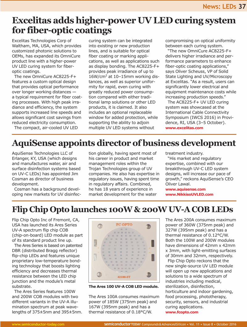
AquiSense Technologies LLC ofErlanger, KY, USA (which designsand manufactures water, air andsurface disinfection systems basedon UV-C LEDs) has appointed JimCosman as director of businessdevelopment. Cosman has a background devel-
oping new markets for UV disinfec-
tion globally, having spent most ofhis career in product and marketmanagement roles within the Trojan Technologies group of UVcompanies. He also has expertise inregulatory issues, having spent timein regulatory affairs. Combined, he has 18 years of experience inmarket development for the water
treatment industry. “His market and regulatory
expertise, combined with ourbreakthrough UV-C LED systemdesigns, will increase our pace ofgrowth,” reckons AquiSense’s CEOOliver Lawal. www.aquisense.comwww.NikkisoUVLED.com
Flip Chip Opto Inc of Fremont, CA,USA has launched its Ares SeriesUV-A spectrum flip chip COB (chip-on-board) LED module as partof its standard product line up. The Ares Series is based on patented
DBR (distributed Bragg reflector)flip-chip LEDs and features uniqueproprietary low-temperature bond-ing technology that boosts lightingefficiency and decreases thermalresistance between the LED chipjunction and the module’s metalsubstrate. The Ares Series features 100W
and 200W COB modules with twodifferent variants in the UV-A illu-mination spectrum at peak wave-lengths of 375±5nm and 395±5nm.
The Ares 100A consumes maximumpower of 185W (375nm peak) and167W (395nm peak) and has athermal resistance of 0.18°C/W.
The Ares 200A consumes maximumpower of 360W (375nm peak) and327W (395nm peak) and has athermal resistance of 0.12°C/W.Both the 100W and 200W moduleshave dimensions of 42mm x 42mmx 3mm, with light-emitting surfacesof 30mm and 32mm, respectively. Flip Chip Opto reckons that the
new single-source UV LED modulewill open up new applications andsolutions to a wide spectrum ofindustries including medical, sterilization, disinfection, horticulture and indoor gardening,food processing, phototherapy,security, sensors, and industrialcuring applications. www.fcopto.com
Flip Chip Opto launches 100W & 200W UV-A COB LEDs
News: LEDs
www.semiconductor-today.com semiconductorTODAY Compounds&AdvancedSilicon • Vol. 11 • Issue 8 • October 2016
37
Excelitas Technologies Corp ofWaltham, MA, USA, which providescustomized photonic solutions toOEMs, has expanded its OmniCureproduct line with a higher-powerUV LED curing system for fiber-optic coatings. The new OmniCure AC8225-F+
features a custom optical designthat provides optical performanceover longer working distances — a typical requirement for fiber coat-ing processes. With high peak irra-diance and efficiency, the systemsupports increased line speeds andallows significant cost savings fromreduced electricity consumption. The compact, air-cooled UV LED
curing system can be integratedinto existing or new productionlines, and is suitable for opticalfiber coating or marking appli-cations, as well as applications suchas display bonding. The AC8225-F+provides peak irradiance of up to16W/cm2 at 10–15mm working dis-tances, as well as superior unifor-mity for rapid, even curing withgreatly reduced power consump-tion compared with either tradi-tional lamp solutions or other LEDproducts, it is claimed. It alsoincludes an optional replaceablewindow for added protection, whilesupporting the ability to adjoinmultiple UV LED systems without
compromising on optical uniformitybetween each curing system. “The new OmniCure AC8225-F+
delivers higher irradiance and per-formance parameters to enhancefiber-optic coating applications,”says Oliver Scheuss, VP of SolidState Lighting and UV/Microscopyat Excelitas. “As a result, users cansignificantly lower electrical andequipment maintenance costs whileincreasing production speeds.” The AC8225-F+ UV LED curing
system was showcased at theInternational Cable ConnectivitySymposium (IWCS 2016) in Provi-dence, RI, USA (3–5 October). www.excelitas.com
Excelitas adds higher-power UV LED curing systemfor fiber-optic coatings
AquiSense appoints director of business development
The Ares 100 UV-A COB LED module.
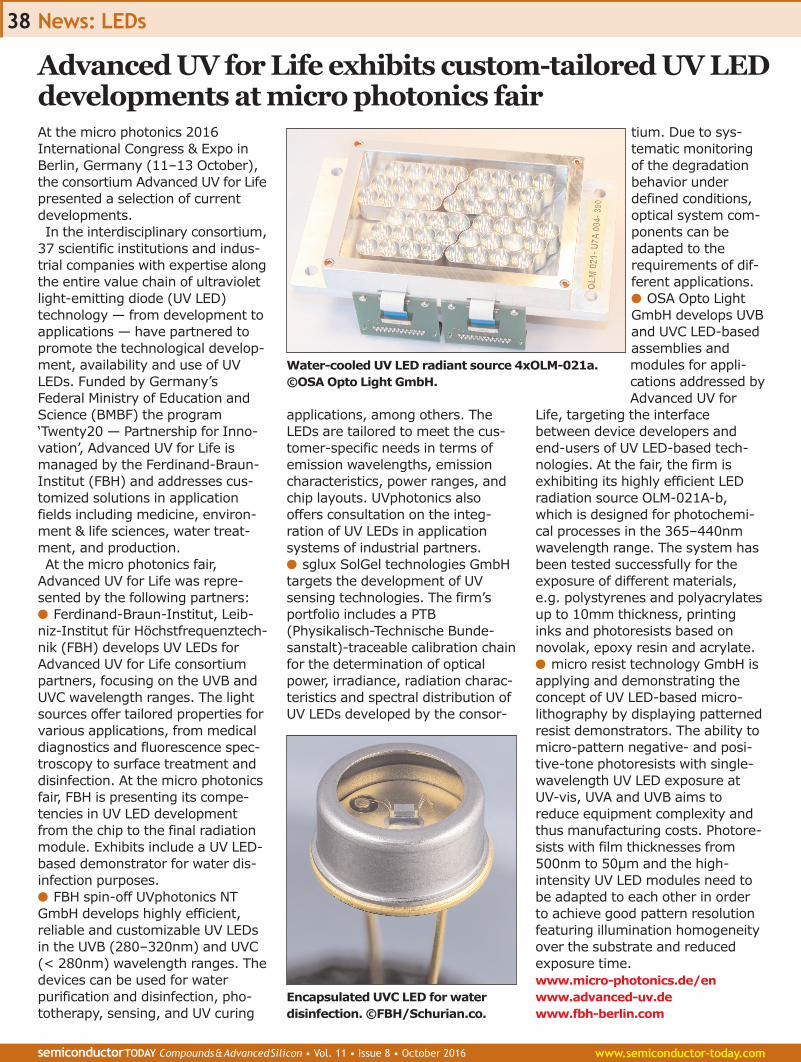
News: LEDs
semiconductorTODAY Compounds&AdvancedSilicon • Vol. 11 • Issue 8 • October 2016 www.semiconductor-today.com
38
At the micro photonics 2016 International Congress & Expo inBerlin, Germany (11–13 October),the consortium Advanced UV for Lifepresented a selection of currentdevelopments. In the interdisciplinary consortium,
37 scientific institutions and indus-trial companies with expertise alongthe entire value chain of ultravioletlight-emitting diode (UV LED) technology — from development toapplications — have partnered topromote the technological develop-ment, availability and use of UVLEDs. Funded by Germany’s Federal Ministry of Education andScience (BMBF) the program‘Twenty20 — Partnership for Inno-vation’, Advanced UV for Life ismanaged by the Ferdinand-Braun-Institut (FBH) and addresses cus-tomized solutions in applicationfields including medicine, environ-ment & life sciences, water treat-ment, and production. At the micro photonics fair,
Advanced UV for Life was repre-sented by the following partners: ● Ferdinand-Braun-Institut, Leib-niz-Institut für Höchstfrequenztech-nik (FBH) develops UV LEDs forAdvanced UV for Life consortiumpartners, focusing on the UVB andUVC wavelength ranges. The lightsources offer tailored properties forvarious applications, from medicaldiagnostics and fluorescence spec-troscopy to surface treatment anddisinfection. At the micro photonicsfair, FBH is presenting its compe-tencies in UV LED developmentfrom the chip to the final radiationmodule. Exhibits include a UV LED-based demonstrator for water dis-infection purposes. ● FBH spin-off UVphotonics NTGmbH develops highly efficient,reliable and customizable UV LEDsin the UVB (280–320nm) and UVC(< 280nm) wavelength ranges. Thedevices can be used for waterpurification and disinfection, pho-totherapy, sensing, and UV curing
applications, among others. TheLEDs are tailored to meet the cus-tomer-specific needs in terms ofemission wavelengths, emissioncharacteristics, power ranges, andchip layouts. UVphotonics alsooffers consultation on the integ-ration of UV LEDs in applicationsystems of industrial partners.● sglux SolGel technologies GmbHtargets the development of UVsensing technologies. The firm’sportfolio includes a PTB(Physikalisch-Technische Bunde-sanstalt)-traceable calibration chainfor the determination of opticalpower, irradiance, radiation charac-teristics and spectral distribution ofUV LEDs developed by the consor-
tium. Due to sys-tematic monitoringof the degradationbehavior underdefined conditions,optical system com-ponents can beadapted to therequirements of dif-ferent applications.● OSA Opto LightGmbH develops UVBand UVC LED-basedassemblies andmodules for appli-cations addressed byAdvanced UV for
Life, targeting the interfacebetween device developers andend-users of UV LED-based tech-nologies. At the fair, the firm isexhibiting its highly efficient LEDradiation source OLM-021A-b,which is designed for photochemi-cal processes in the 365–440nmwavelength range. The system hasbeen tested successfully for theexposure of different materials,e.g. polystyrenes and polyacrylatesup to 10mm thickness, printinginks and photoresists based onnovolak, epoxy resin and acrylate. ● micro resist technology GmbH isapplying and demonstrating theconcept of UV LED-based micro-lithography by displaying patternedresist demonstrators. The ability tomicro-pattern negative- and posi-tive-tone photoresists with single-wavelength UV LED exposure atUV-vis, UVA and UVB aims toreduce equipment complexity andthus manufacturing costs. Photore-sists with film thicknesses from500nm to 50µm and the high-intensity UV LED modules need tobe adapted to each other in orderto achieve good pattern resolutionfeaturing illumination homogeneityover the substrate and reducedexposure time. www.micro-photonics.de/en www.advanced-uv.de www.fbh-berlin.com
Advanced UV for Life exhibits custom-tailored UV LEDdevelopments at micro photonics fair
Encapsulated UVC LED for waterdisinfection. ©FBH/Schurian.co.
Water-cooled UV LED radiant source 4xOLM-021a.©OSA Opto Light GmbH.

News: LEDs
www.semiconductor-today.com semiconductorTODAY Compounds&AdvancedSilicon • Vol. 11 • Issue 8 • October 2016
39
At micro photonics 2016, Berlin’sFBH presented novel developmentsof its diode lasers and UV LEDs. FBH develops diode lasers and LEDs
from the chip through to the finalmodule, and increasingly advancesthese devices up to the operationalsystem. Customers and partnerscan hence test their developmentsin the respective application. FBH’scustomized diode lasers open up avariety of applications, from mater-ial analytics, sensors, and displaytechnology to materials processing.Similarly, UV LEDs (focusing on theUV-B and UV-C spectral range) canbe adjusted flexibly to the require-ments. Applications cover medicaldiagnostics and fluorescence spec-troscopy as well as surface treat-ment and disinfection. FBH’s exhibits included:
Industrial diode laser moduleswith optical fiber connection FBH offers compact diode lasermodules that allow customers touse high-brilliance laser radiation intheir applications. Due to an integ-rated single-mode fiber (SMF) port,the matchbox-sized modules canbe installed into different systems.Efficient laser light sources are henceavailable for the near-infrared spectral range, delivering diffraction-limited radiation with narrow band-width where it is needed. So far, three different module
types have been demonstrated. For modules with both high outputpower (>2W) and high spectralradiance, FBH has expanded theavailable wavelengths to the spectralrange 804–1064nm. This setup canbe transferred to wavelengths up to1180nm and is thus suitable forpumping solid-state lasers as well asfor frequency doubling. Additionally,seed-laser modules emitting at633nm and 1180nm have beendemonstrated that deliver outputpower of >20mW ex fiber, featuringan optical micro-isolator and polari-zation-maintaining SMF (PM-SMF)at the output. A polarization extinc-tion ratio of more than 20dB wasshown for modules with PM-SMF
output in the spectral range633–1180nm. As a third design, anamplifier module emitting at1180nm with PM-SMF input andfree-space output yielding >1Woutput power has been developed.By coupling light from a seed-lasersource into the PM-SMF, this radiationcan be easily amplified, says FBH.The principle is also transferable toother wavelengths. Tailored, flexible picosecondlight impulse source With PLS 1030, FBH offers an effi-cient pulsed laser source that usesin-house-developed optical andelectronic components. The lasersystem is currently being optimizedso that all functionalities are integ-rated in just one compact device,instead of two separate componentspreviously, offering improved capabil-ity. The all-in-one PLS 1030 deliversultra-short light impulses at a wave-length of 1030nm within an adjustabletime range of 5–15ps and providesfreely selectable repetition frequen-cies, in a range of hertz to megahertz.Pulse peak performance is over 20W.Due to these properties, the lasersource is suited to applications inmaterials processing, especially inconnection to fiber amplifiers, forbiomedical examinations based onfluorescence spectroscopy, and formobile LIDAR systems. The devicecan be equipped with semiconductorcomponents for 1030nm and 1064nm,but can be flexibly transferred toother wavelengths. It consists of amode-locked laser with a repetitionrate around 4GHz, a pulse pickerelement, and an optical amplifier.Electronic control has also beendeveloped using FBH’s gallium nitride(GaN) transistors. As a result, shortimpulses can be flexibly selectedfrom single to multiple serial pulses(burst mode) and amplified. ThePLS 1030 is computer-operated toenable it to be easily integrated intovarious laser systems, ensuringstable and user-friendly operation. Higher brilliance and outputpower for diode lasers and bars FBH develops high-brilliance diode
lasers various designs and packagesspanning 630–1180nm wavelengths.Single emitters with a stripe widthof 90µm reach peak brilliance of3.5W/mm-mrad. Smaller stripewidths deliver up to >6W/mm-mrad(for 20–30µm apertures) — again arecord. For materials processing,FBH has developed custom arraysfor spectral beam combining, con-sisting of five brilliant DFB laserswith 30µm apertures, each giving5W output with 50% efficiency. The emitter-to-emitter wavelengthspacing is 2.5nm. Future activitiesaim to improve efficiency, reliabilityand output power. Record resultshave recently been achieved fromnovel QCW bars that demonstrate60% efficiency when operated with1kW output at 15°C (rising to 70%at –70°C). Module for water disinfection Using in-house 262nm LEDs, FBHhas designed a rod-shaped modulefor water disinfection that aims toreplace conventional low-pressuremercury vapor lamps. UV LEDshave higher lifetimes, are mainte-nance-free and, since they do notrequire toxic chemicals like mercury,are environmentally friendly (mer-cury lamps need to be disposed ofsafely after a few thousand hoursof operation). Wavelength andemission characteristics can also beadjusted specifically to the desiredapplication. FBH’s demonstrator(debuted at micro photonics) uses40 LEDs, each delivering opticaloutput of 1.7mW; the average irra-diation intensity at a distance of 2cmis 2W/m2. The geometry followsconventional flow-through waterdisinfection reactors for treatmentof drinking or process water. TheFBH setup is modularly expandableand adaptable to reactor size. TwoLEDs form an assembly group witha constant-current supply (maximum100mA per LED) and a temperaturetermination for security reasons.Heat is dissipated via a heat pipewith an attached fan. www.fbh-berlin.com/business-areas/diode-lasers/
FBH presents diode laser & UV LED developments

South Korea’s Samsung ElectronicsCo Ltd has launched a line-up ofchip-scale package (CSP) LEDmodules for spotlights and down-lights that features color tunabilityand increased design compatibility. “Our new CSP LED modules pro-
vide an optimal solution for lightingmanufacturers who seek highlycompatible and reliable LED components,” says Jacob Tarn,executive VP, LED business team. The LED modules are Samsung’s
first to incorporate CSP technology,which brings a wide range of light-ing benefits such as significantlyreducing the size of a conventionalLED package. The combination offlip-chip and phosphor coatingtechnology eliminates metal wiresand plastic molds to enable morecompact designs when manufac-turing LED modules and fixtures. The CSP LED modules also deliver
further characteristics that allowseamless tunable color. A color-tunable LED module requires twicethe number of LED packages in cool
and warm temperature, which workin combination on the same boardto create a range of tunable colors.In contrast to conventional plastic-molded LED packages thatinevitably increase the size of themodules, Samsung’s ultra-compactchip-scale LED packages allow themodule size to remain unchanged. The new CSP LED modules are
available in two form factors(19mm x 19mm or 28mm x 28mm)and are designed following Zhagaspecifications, making assemblyconvenient. The modules are alsosaid to provide high-quality lightingin diverse beam angle options(spot, medium, wide) for improved
compatibility with optical solutionsof Samsung’s partners. The modulesare based on CSP LED packagesthat have completed 9000 hours ofLM-80 testing, reducing time tomarket for lighting manufacturers. Samsung is sampling six models
of the new CSP LED module in colorrendering indexes (CRIs) of 80 and90 with varying lumen output, sizeand correlated color temperature(CCT) specifications: i.e. (for 80CRI)the 19mm x 19mm CO10 and CO20(with 9.4W and 18.3W power con-sumption and 1050lm and 2060lmoutput, respectively) and the28mm x 28mm CO30 and CO40(with 27.4W and 36.5W consumptionand 3090lm and 4120lm output,respectively), all with CCT optionsof 2700/3000/3500/4000K, andthe 28mm x 28mm TO10 and TO20(with 9.2–9.8W and 17.7–18.4Wconsumption and 1060/1150lm and1970/2190lm output, respectively),which are color tunable over CCTsof 2700–5000K. www.samsung.com
Samsung launches its first CSP-based LED modules
News: LEDs
semiconductorTODAY Compounds&AdvancedSilicon • Vol. 11 • Issue 8 • October 2016 www.semiconductor-today.com
40
In view of fast-growing demand forchip-scale package (CSP) LED chipsfor TV backlighting, Epistar Corp ofHsinchu Science-based IndustrialPark, Taiwan (the world’s largest LEDepiwafer and chip maker) will expandproduction capacity four-fold in early2017, says Taiwan’s Digitimes. While CSP LED chips were adopted
for direct-type LED-backlit LCD TVs,the adoption in edge-type backlitLCD TVs came much later due totechnological problems, Epistar says.These problems have been solved,and demand for CSP LED chips hastaken off, the firm adds. Monthlyshipments of CSP LED chips haverisen from 5 million units in early
2016 to 230 million, and Epistarclaims a global market share of 30%. Also, Epistar has been developing
quantum dot (QD)-on-chip technol-ogy by combining CSP LED chips withQD technology. It expects QD-on-chipto be adopted for backlighting in60–70” LCD TVs beginning 2017. www.epistar.com.tw
Epistar to quadruple CSP LED chip capacity in early 2017
UK-based LED maker Plessey’s newOrion beam forming module hasbeen shortlisted in two categories(Manufacturer of the Year andEnabling technology of the Year) in the 2016 Lux Awards, which celebrate and reward creativity and sustainability in lighting. Plessey is showcasing the first
standardized product using its Stellar Optic Technology at LuxLive in
London, UK (23–24 November). As a slim-line module for directionallight, the Orion is said to removemany of the restraints typically foundin COB (chip-on-board)-type modules. Awards winners will be announced
at a ceremony on 24 November atThe InterContinental London — The O2, following LuxLive. Plessey isexhibiting for its third year runningand will demonstrate solutions
based on its MaGIC (Manufacturedon GaN-on-Si I/C) LED technologyfor the solid-state lighting market. In booth M8 at LuxLive, Plessey’s
technical and design experts willpresent product demonstrations,providing an opportunity to gain anunderstanding of its latest solutionsfor commercial, industrial, consumerand wearable lighting markets. www.plesseysemiconductors.com/
Plessey shortlisted as finalist in Lux Awards
CO20 CSP LEDmodule
News: LEDs
www.semiconductor-today.com semiconductorTODAY Compounds&AdvancedSilicon • Vol. 11 • Issue 8 • October 2016
41
UK-based lighting and sensingproduct and component makerPlessey has launched its 7070 high-power LED range (PLW7070GA.). The PLW7070 products exploit
Plessey’s MaGIC (Manufactured onGaN-on-Si I/C) technology and pro-vide a high-power LED componentin an industry standard packagefootprint, complementing Plessey’sexisting family of i2LED high-powerproducts. Using its proprietary gallium nitride on silicon (GaN-on-Si)high-voltage technology, Plesseysays that it has been able to use asingle LED die to improve thermalperformance, improve far-fieldimaging and dramatically reducecost over incumbent solutions. Plessey provides components and
solutions spanning the whole light-ing value chain. Lighting systemdesigners and specifiers can accessits design, build and supply chainexpertise from GaN-on-Si blue dieall the way up to complete luminairesand fixtures. The PLW7070GA high-power LED with multiple junctionsintegrated in a single chip elimi-
nates shadow effects and providesoptimized far-field imaging, saysthe firm. Compatible with industry-standard secondary optics andoperating at input currents from350mA to 3A (1–15W power),Plessey’s low-cost, high-power single chip LEDs are available in afull range of correlated color tem-perature (CCT) and color renderingindex (CRI) options for demandingoutdoor and commercial lightingapplications. “The PLW7070 range has been
designed using our unique integratedmulti-junction die architecture thatprovides us with a differentiatedsolution for a diverse range of high-power applications in high-bay,floodlighting, street lighting, spotlighting and down lighting, in addi-tion to portable torches and lamps,”says director of sales Giuliano Cassataro. “The move for designersto mid-power products because oflow cost can now be reversed, aswe can provide solutions where theoverall fixture costs are up to 50%lower. GaN on silicon is really start-
ing to come into his own,” he adds. “The key features and benefits we
bring to customers and the LEDlighting market with the Plessey7070 range is a custom aluminiumnitride ceramic lensed package withan industry-standard solder patternand footprint,” says chief technologyofficer Dr Keith Strickland. “Its lowthermal resistance of less than2°C/W, combined with a high maximum junction temperature of135°C for good thermal managementin demanding thermal environments,is critical in heat management,” he adds. “Using a single GaN/Simulti-junction chip for 12V and 24Voperation, Plessey is setting a newbenchmark for far-field imagingand the use of secondary optics innarrow-beam-angle applications,”he claims. “Superb maintenance ofluminous flux is possible over awide temperature range, and thein-built ESD protection providesstable yield through system manu-facture and operation.” www.plesseysemiconductors.com/led-plessey-semiconductors.php
Plessey launches single-chip high-power 7070 LEDs
Plessey has announced the firststandard LED module based on itsStellar beam-forming technology.The new standard module is saidto open up opportunities for cre-ativity in industrial and architec-tural lighting design. Plessey’s Orion PLWS3000 series
is an LED array module deliveringmore than 3000 lumens, integ-rating LED and optics into a mod-ule just 5.6mm thick and 82mm indiameter. Alternative solutionstypically require optics that areusually 100mm deep and 111mmin diameter for a comparable lightoutput and beam. Plessey saysthat it has achieved this size andperformance by combining itsStellar beam-forming optics andgallium nitride on silicon (GaN-on-Si) LED technology.Plessey expects applications of the
module to be in the design oftrack, retail, architectural, high-intensity, spot and directionallighting, and especially architec-tural applications. The reduced form factor of the
Orion eliminates design con-straints and allows more designfreedom for lighting designers,says chief technology officer DrKeith Strickland. “Typically, usingCOB [chip-on-board]-type LEDs or modules makes it difficult tocontrol color over angle, forcingdesigners to make fixtures muchlarger in size. The Orion, with Stellar beam-forming technology,represents the next phase in LEDlighting with low cost, high effi-ciency and greater control of light.Greater control over the directionand quality of light is a crucial ele-ment in retail, industrial, hospital-
ity and outdoor lighting; this, com-bined with the slim-line design andimpressive thermal characteristics,means we provide lighting design-ers and architects far more designfreedom,” he adds. “The Orion focuses on replacing
design limitations with opportuni-ties, thus providing lightingdesigners with a new level ofdesign freedom,” says PaulDrosihn, Plessey’s head of ModularProducts. “The size/performanceenvelope we have achieved allowsindustrial high-bay and architec-tural luminaires used in high-endoffices, homes and retail outlets tobe created in a new way,” he adds.“With a particular emphasis onimproving the thermal characteris-tics, the heat-sink can also bereduced in size, allowing the endfixture to be less obtrusive.”
Beam-forming LED module using Stellar optical technology
News: LEDs
semiconductorTODAY Compounds&AdvancedSilicon • Vol. 11 • Issue 8 • October 2016 www.semiconductor-today.com
42
On 29 September, Nichia filed arequest in the Düsseldorf DistrictCourt for a preliminary injunctionagainst Mouser Electronics Inc,alleging that the white LED product334-15/X1C5-1QSA made byEverlight and distributed by Mouser
in Germany infringes Nichia’s YAGpatent EP 936 682 (DE 697 02 929). The court has now admitted
Nichia’s arguments that the productinfringes claim 1 of Nichia’s YAGpatent, and has hence granted thepreliminary injunction.
Due to the particular urgency, thepreliminary injunction was grantedex parte (without the prior hearingof Mouser) and served to Mouseron 7 October. Nichia notes that thisis a preliminary measure that canstill be remedied by Mouser.
On 18 October, Nichia Corp ofTokushima, Japan filed a patentinfringement lawsuit with the TokyoDistrict Court against Taiwan-basedsmartphone vendor HTC’s Japanesesubsidiary HTC Nippon Corp and its
distributor Kanematsu Communica-tions Ltd alleging that the whiteLEDs in the HTC Desire 626 smart-phone sold in Japan incorporatewhite LED that infringe on Nichia’spatents JP5177317 and JP5610056.
Nichia is seeking an injunction toindemnify the patent infringementas well as compensation for damages.Neither HTC nor HTC Nippon haveyet responded to the accusation. www.nichia.co.jp
Following a lawsuit filed by Nichia,the Tokyo District Court has ruledthat the importation/sale in Japanby Tachibana Eletech Co Ltd and
E&E Japan Co Ltd of the 1254 seriesand 7344 series blue LEDs made byTaiwan’s Everlight Electronics Co Ltdconstituted infringement of Nichia’s
Japanese patent no. 2780618. Thecourt has ordered Tachibana andE&E to pay Nichia monetary dam-ages caused by their infringement.
Tokyo District Court rules that Tachibana Eletech infringed Nichia’s patent by selling Everlight LED products
Nichia files white LED patent infringement lawsuitagainst HTC Nippon and its distributor Kanematsu
Court grants preliminary injunction against Mouserregarding Everlight product based on Nichia YAG patent
Epistar Corp of Hsinchu Science-based Industrial Park, Taiwan (theworld's largest manufacturer of LEDepiwafers and chips) has signed alicense agreement for its filamentpatents to be used in the productsof Super Trend Lighting (Group) Ltd. Epistar holds key intellectual property
regarding LED filament technologyused in making LED filament bulbs.The patents relate to, among otherthings, LED filament structures,and light-emitting products usingLED filaments. The patent portfoliocovers Taiwan, China, USA, Europeand other territories.
Super Trend is the existinglicensee with the right to manufac-ture products covered by Epistar’sLED filament patents. Epistar saysthat it will continue to update itslicensee list. www.stll.com www.epistar.com.tw
Epistar has agreed to settle itspatent litigation against Adamax Inc(trading as Newhouse Lighting)filed on 30 August in the US Dis-trict Court for the Northern Districtof California alleging infringementof Epistar’s light-emitting diode filament patents (US Patent Nos.6,346,771, 7,489,068, 7,560,738,8,240,881, 8,344,353, 8,791,467,9,065,022).
The patents relate to, amongother things, LED filament structuresand light-emitting products usingLED filaments. The complaintasserted that Newhouse Lightingproducts and technology infringedEpistar patents and sought injunc-tive relief to halt further sales. Under the terms of the settlement,
Epistar will release Adamax for thepast sales of its LED filament
products under the patents-in-suit.In addition, Adamax will pay ongoing royalties based on itssales of products for Epistarpatents-in-suit. Epistar says that the settlement
protects its investment in R&D onadvanced LED technologies at thecore of its business. www.newhouselighting.com www.epistar.com.tw
Epistar settles US patent infringement lawsuit against Adamax
Epistar licenses LED filament patents to Super Trend

Take trimethylgallium for instance, key to making the light-emitting semiconductor material found in an LED. Umicore produces it at low waste, high efficiency.
Our high purity metalorganics are taking sustainability a step further; we think out of the box and beyond electronics. Thinking greener isn‘t just a state of mind, it‘s part of our culture. Check out our product list for more hits.
Go for efficiency. Go for Umicore
We‘re playing your song: “Green is the new Black.”
www.chemistry.umicore.com
16-35-059 Semiconductor 282x213 LED.indd 1 05.08.16 11:04

News: LEDs
semiconductorTODAY Compounds&AdvancedSilicon • Vol. 11 • Issue 8 • October 2016 www.semiconductor-today.com
44
BluGlass Ltd of Silverwater, Australia— which was spun off from the III-nitride department of MacquarieUniversity in 2005 to develop alow-temperature process usingremote plasma chemical vapordeposition (RPCVD) to grow mater-ials including gallium nitride (GaN)and indium gallium nitride (InGaN)on glass substrates — has completedthe technology demonstration out-lined in Phase I of the exclusiveevaluation agreement (unveiled in
March) with LED maker Lumileds. The Phase I demonstration of Blu-
Glass’ unique low-temperatureRPCVD technology involved deliver-ing technical milestones previouslyunachieved by RPCVD. “The suc-cessful demonstration of thesemilestones has broken exciting newground for the RPCVD technologydevelopment,” says chief technol-ogy officer Dr Ian Mann. “These ini-tial demonstrations indicate thatthe novel implementation of RPCVD
we are working on with Lumiledshas certain advantages over thestandard MOCVD process.” BluGlass is commercializing RPCVD
for the LED and power electronicsindustries. The firm has developedpatented hardware and processestargeting the production of moreefficient semiconductor devices atlower cost. BluGlass entered into itsPhase I Evaluation with industryleader, Lumileds this year. www.bluglass.com.au
BluGlass and Lumileds move to Phase II ofevaluation agreement after completing Phase I Lumileds to further investigate integration of BluGlass’ RPCVD technology into LED applications
The US Department of Energy(DOE) has announced the fundingopportunity DE-FOA-0001613,‘Solid-State Lighting AdvancedTechnology R&D—2017’), in whicha total of up to $10m is directedtoward all three existing DOE SSLR&D program areas: ● Core Technology Research —applied research aiming to demon-strate scientific principles, technicalapplication, and application benefits,
and encompassing scientific effortsthat focus on new knowledge orunderstanding of the subject understudy, with specific application to SSL; ● Product Development — thedevelopment of commercially viable,state-of-the-art SSL materials,devices or luminaires using conceptsfrom basic and applied research; ● US Manufacturing — research todevelop advanced manufacturingapproaches to reduce the cost of
SSL sources and luminaires andimprove product consistency andquality, with the additional benefitof supporting the development ofUS-based manufacturing. The DOE will select up to 10 proj-
ects. Concept papers are due by 14 November, and full applicationsare due by 10 January 2017. https://eere-exchange.energy.gov/#FoaId68693dde-c993-459d-8763-d3020ab40f6e
LED maker Lumileds of San Jose,CA, USA has launched the LUXEON5050, a multi-die high-power pack-age that provides high flux at highefficacy, enabling system designersto reduce LED count and cost inoutdoor and indoor fixtures. “The LUXEON 5050 is the superior
choice for outdoor and directionallamp applications that demand highefficiency and cost-effective designtogether with precise beam control,”reckons product manager Ivan Tsoi.For example, in outdoor applications,the source delivers luminous efficacyof >155lm/W at typical drive current
of 160mA (4000K, 70CRI) and>180lm/W at 80mA. For indoorspotlights and downlights, the LUX-EON 5050 can achieve >130lm/Wat 160mA (3000K, 80CRI).The LUXEON 5050 is offered in a
range of color temperatures
(2700–5700K) at 70, 80 and 90CRI(color rendering index). The sourceis driven at a voltage of 24V,enabling the use of low-cost andhigh-efficiency drivers for all solid-state lighting applications. The surface-mount device package
has a thermal resistance of 1.9K/W,which greatly reduces thermalmanagement needs. Finally, theLUXEON 5050 utilizes a small roundlight-emitting surface (4.6mm),simplifying optical design and mak-ing it easier to achieve high center-beam candle power. www.lumileds.com/LUXEON5050
US DOE announces 2017 solid-state lighting R&D funding opportunity
Lumileds launches multi-die LED, cutting cost-per-lumenLUXEON5050LED

KEEPING AN EYE ON THE FUTURE
www.evatecnet.com
ADVANCED PACKAGING • HP OPTICS • MEMS • OPTOELECTRONICS • POWER DEVICES • WIRELESS • THE THIN FILM POWERHOUSE
MORE INFO
Evatec brings you advanced thin fi lm productionsolutions for Advanced Functionality Materials
From new high piezoelectric coeffi cient materials like AlScN to highly
aligned NiFe soft magnetic layers or complex optical interference coatings,
Evatec sputter platforms and processes help you keep an eye on the
future. Advanced Process Control (APC) technologies bring precision and
throughput to the deposition of new Advanced Functionality Materials
in Wireless, MEMS and LED technologies. To fi nd out more about
Evatec processes and platforms visit www.evatecnet.com
RADIANCE SPUTTER CLUSTER MSP 1232 LLS EVO II LOAD-LOCK SPUTTER CLUSTERLINE® 300 II SPUTTER SOLARIS S380 SPUTTER
News: LEDs
semiconductorTODAY Compounds&AdvancedSilicon • Vol. 11 • Issue 8 • October 2016 www.semiconductor-today.com
46
For its fiscal first-quarter 2017 (to25 September 2016), Cree Inc ofDurham, NC, USA has reportedrevenue of $371m, down 4% on$388.4m last quarter and down13% on $425m a year ago, but inthe upper half of the $356–378mtarget range. Of this, discontinued operations
contributed $49.9m (up on $30.9mlast quarter and $43.9m a year ago,and above the targeted $46–48m).In July, Cree agreed for Germany’sInfineon Technologies AG to buy itsWolfspeed business (which includesthe Power & RF product lines thathad historically been reported as aseparate operating segment, plusthe non-LED materials product linepreviously reported within the LEDsegment). Continuing operations contributed
$321.3m (down 10% on $357.5mlast quarter and 16% on $381.5ma year ago, but in line with theexpected $310-330m). Specifically,Lighting Product revenue (mainlyLED lighting systems and bulbs) was$183.8m (57% of total revenue),down 7.4% on $198.4m last quarterand 26% on $248m a year ago.LED Product revenue was $137.5m(43% of total revenue), down13.6% on $159.1m last quarter butup 3% on $133.5m a year ago. On a non-GAAP basis, gross margin
was 28.8%, down from 30.8% last quarter. Gross margin fromcontinuing operations fell from28.2% to 27.7%. Specifically, LEDProduct margin was 30.4%, downfrom 35.1% last quarter, but at theupper end of the targeted range.However, Lighting Product marginwas 26.8%, up from 25.8% lastquarter (with gross margins forcommercial lighting and consumerlighting both improving). “We delivered solid results in fiscal
Q1, as Lighting, LED Products andWolfspeed all achieved revenue andgross margins that were in line withour targets,” says chairman & CEOChuck Swoboda. “We madeprogress improving lighting margins
in both our commercial and con-sumer product lines in the quarter.” Operating expenses (OpEx) for
continuing operations were $80m(at the low end of the target range,primarily due to lower variablesales cost and the timing of IT litigation cost, some of which isexpected to shift to Q2). Net income has fallen further, from
$21.3m ($0.21 per diluted share) a year ago and $18.9m ($0.19 perdiluted share) last quarter to$15.2m ($0.15 per diluted share).However, this is towards the upperend of the $10-16m ($0.10-0.16per diluted share) guidance range. Net income from continuing oper-
ations was $9.5m ($0.09 perdiluted share), down from $14.7m($0.14 per diluted share) a year ago,but in the upper half of the targetedrange of $6–11m ($0.06–0.11 perdiluted share). Net income fromdiscontinued operations was $5.7m($0.06 per diluted share), down from$6.6m ($0.07 per diluted share) a year ago, but above the targetedrange of $4–5m ($0.04–0.05 perdiluted share). Cash generated from operations
has fallen from $64.6m last quarterto $18.1m. In addition to patentspending of $2.3m (down further,from $4.3m a year ago and $3.4mlast quarter), spending on property,plant & equipment (PP&E) has beencut further, from $49.9m a yearago a year ago and $20.3m lastquarter to $19.3m. Total capitalexpenditure has hence been cutfurther, from $34.7m a year agoand $23.7m last quarter to $21m,including $10m for Wolfspeed. Free cash flow was hence –$3.5m(improving on –$7.4m a year ago).During the quarter, Cree spent$36m to re-purchase 1.5 millionshares and about $3m for the year-one earn-out achieved fromthe acquisition of APEI. Overall,consolidated cash and investmentsfell by $16m to $589m or, net ofline of credit borrowings, by $43mto $402m. At the end of the quarter,
Cree had $187m outstanding on itsline of credit. During fiscal Q1/2017, Cree
launched the following new LEDproducts: the next-generationhigher-power XLamp XP-L2 LED(with twice the lumens-per-area);the XLamp XQ-E and XP-E HighEfficiency (HE) Photo Red LEDs; theQLS6A and QLSB6 LEDs; andbrighter MHB LEDs (for commercialoutdoor lighting applications). Cree also launched lighting products
including the HXB LED IndustrialHigh Bay fixture (which uses SC5LED technology); a new 130lm/WZR troffer product; the Essentia byCree LED Surface Wrap; a high-performance version of the CPYcanopy fixture; and the new GEN4family of next generation LED bulbs. For fiscal second-quarter 2017
(ending 25 December 2016), Cree targets revenue of $360–380mand net income of $13–19m($0.13–0.19 per diluted share). For continuing operations, revenue
is targeted to be level at $310–330m,with both Lighting and LED roughlylevel as Cree continues to rebuildcommercial lighting order momentumand operate in a very competitiveLED market. Gross margin shouldalso be similar to fiscal Q1, withimprovement for Lighting offsetslightly by LED Products due to lowertargeted production volumes inCree’s LED factory (to help rebalanceits commercial lighting inventory).Operating expenses should rise by$2m due to promotional spendingrelated to Cree’s GEN4 bulb launchand incremental IP litigationsspending, as well as $1.5m of sharedservice costs supporting Wolfspeedoperations (which will be mostlyreimbursed for a period of timeafter closing, under a transitionservices agreement with Infineon).Net income is targeted to be $4–10m($0.04–0.10 per diluted share). For discontinued operations, Cree
expects revenue to be steady at$50m, and net income to be $9m($0.09 per diluted share), including
Cree’s gross margin aided by improvements in Lighting Commercial lighting order momentum continues to rebuild

News: LEDs
www.semiconductor-today.com semiconductorTODAY Compounds&AdvancedSilicon • Vol. 11 • Issue 8 • October 2016
47
a $4m benefit net of tax ($0.04 perdiluted share) from the full impact ofnot including depreciation or amorti-zation expense from long-lived assets. “The business fundamentals are
improving in Lighting as we seeimproved customer service levels,increased channel coating activityand better gross margins,” noteschief financial officer Mike McDevitt.“But it will take several quarters to seethe full benefit in our financial results.” “We’re still working to earn back
share with our lighting agent anddistribution channel partners andtranslate that effort to new projectsand increased orders,” says Swo-boda. “The leading indicators areencouraging, and we’re makinginvestments in people and systemsto further improve commerciallighting performance,” he adds. Accordingly, Cree has appointed
Danny Castillo as president, Light-ing (effective 7 November),responsible for both commercialand consumer lighting business. In addition, David Elien (a lightingindustry veteran who has led thecommercial lighting business forthe last two quarters) will continueto run this business as part of thenew lighting organization reportingto Castillo. “We’re expanding ourteam, bringing in experienced lead-ers who understand the uniqueaspects of the traditional lightingindustry and sales channels andcomplement our strength and innovation,” says Swoboda. “While we forecast the short-term
increase in Q2 OpEx, in general wetarget company operating expensesto grow slower than our revenue overthe next year, which should drivesome incremental margin leverage,”says Swoboda. “To enable our revenue and profit goals, we must
continue to innovate in all businesssegments to differentiate our prod-ucts in the market and improve thecustomer experience and servicelevels across the company.” For fiscal 2017, Cree targets
Lighting and LED capital spendingof $55m to support continuingoperations. Until the sale of Wolfspeed is completed, Cree willcontinue to invest capital to supportthe business, including capitalspending of $10m for fiscal Q2/2017(in line with previous guidance). Cree continues to target fiscal 2017
free cash flow of $100m, whichmay change depending on the timing of the Wolfspeed sale. Cree and Infineon are continuing
to work together to obtain the customarily required regulatoryapprovals in various jurisdictions,including foreign and domesticanti-trust approvals, as well asCFIUS approval. In late September,the parties received a secondrequest for additional informationfrom the US Federal Trade Commis-sion (FTC). Cree and Infineon stillaim to close the transaction aroundthe end of 2016. “This will furtherstrengthen our balance sheet tofund share repurchases in the near-term and pursue inorganic lightinggrowth in the medium to longerterm,” says Swoboda. “Our second priority is driving
top-line growth for our LED lightingbusiness. Over the next year, wetarget growing core commerciallighting revenue from current levelsand in line with the market, whilepotentially adding to that growththrough product line expansion,”says Swoboda. “Our corporatedevelopment team is working toevaluate lighting growth opportuni-ties through potential M&A. But we
don’t target any deals in the nextfew quarters, as we give the newlighting leadership team time to buildmomentum for the core business.”“Customer service fundamentals
in commercial lighting have clearlyimproved over the last two quarters,which is the first step to rebuildingorder momentum,” continues Swoboda. “The new products wereleased in [fiscal] Q4 are startingto gain initial project wins. But ittypically takes nine-months toactually gauge market traction fornew products,” he adds. “The consumer product transition
to GEN4 is proceeding as expectedwith the initial loading orders com-bined with demand for our previ-ously generation a little higher thanforecast. Our new GEN4 LED bulbcontinues to provide the premiumlight and quality that consumersexpect from the Cree brand, but ata lower price point and better valuethan our previous generation. Thenew bulb is targeted to providesome incremental margin improve-ment for the consumer productline, which we are using in thenear-term to fund an expandedmarketing program to support thenew product launch,” Swoboda says.The new bulbs have been shippedto stores, but are still in the processof being fully merchandised. “The LED business has performed
well over the last year,” notes Swoboda. “The market remainsvery competitive and we continue tofocus our efforts on the applicationswhere our technology can add themost value to the customer. We’realso working on some mid-to-longerterm programs that could expandthe LED business in future years forboth existing and new applications.”www.cree.com
Cree has appointed Daniel Castilloas president, Lighting, reporting tochairman & CEO Chuck Swoboda. Castillo joins from Eaton Corp,
where he was senior VP, Oil, Gasand IEC Assemblies. Previously,
he held leadership roles in lightingand other electrical product areasat both Cooper Industries andGeneral Electric. “We have made tremendous
progress over the past several
years building a successful LEDlighting business,” says Swoboda.Castillo brings “valuable industryexpertise and proven businessleadership to Cree as we scale thebusiness to the next level,” he adds.
Cree appoints president of Lighting business

LED chip, lamp and lighting fixturemaker Cree Inc of Durham, NC,USA has launched the XLamp XQ-Eand XP-E High Efficiency (HE)Photo Red LEDs. With up to 21%higher output than previous gener-ations of XQ-E and XP-E Photo RedLEDs, they enable horticulturelighting manufacturers to deliverhigher-performance products,reduce luminaire size and lowersystem cost, says the firm. “The XQ-E family provides a unique
combination of ultra-compact pack-age, high output and wide range ofhorticulture-optimized colors,” saysMichael Naish, director at high-thermal-conductivity substrate firmRusalox. “Using XQ-E LEDs with ourunique AlumOxide technology, ourcustomers can create luminairesthat use half the power of conven-tional HPS luminaires, as well asbeing smaller and weighing lessthan incumbent technologies,” hereckons. “The higher-performingXQ-E High Efficiency Photo Red LEDwill enable customers to quicklyreduce the power consumption oftheir current design even furtherfor faster payback periods.”
The XQ-E High Efficiency PhotoRed LED delivers PPF (photosyntheticphoton flux) of up to 5.39μmol/s at85°C from a package footprint ofjust 1.6mm x 1.6mm. Its ratio ofoutput to size is more than doublethat of theclosest com-petitor, it isclaimed. TheXP-E High Effi-ciency PhotoRed LED deliv-ers up to6.08μmol/secPPF output at85°C and issaid to be thefirst LED tobreak the 1W
radiant flux barrier at 85°C. “The new XQ-E and XP-E High
Efficiency Photo Red LEDs bringCree’s latest high-power performancebreakthroughs to horticulture light-ing, with twice the PPF density andhigher output than all other avail-able LEDs,” claims Dave Emerson,VP & general manager for CreeLEDs. “Our technology enables cus-tomers to create high-performance,long-life luminaires that drive theadoption of LEDs in this emergingapplication,” Emerson adds. Cree’s portfolio of LEDs optimizedfor horticulture also includes White, Royal Blue and Far Red color options. Both XQ and XP LEDs for horticulture
are based on Cree’s ceramic high-power technology, which can deliverR90 lifetimes over 100,000 hours,even at the extreme temperatureof 105°C. In addition, horticulturelighting manufacturers can immedi-ately take advantage of the existingecosystem of drivers and opticsproven to work with the XQ and XPplatforms to accelerate their timeto market. www.cree.com/xlamp/horticulture
The XQ-Efamily providesa uniquecombination ofultra-compactpackage, highoutput andwide range ofhorticulture-optimizedcolors
News: LEDs
semiconductorTODAY Compounds&AdvancedSilicon • Vol. 11 • Issue 8 • October 2016 www.semiconductor-today.com
48
Cree has launched the QLS6A andQLS6B LEDs, which are claimed tobe the brightest side-view LEDsoptimized for gaming applications,yielding up to 66% higher luminousintensity than other side-view LEDs.Expand the firm’s range of high-brightness LEDs optimized forindoor and outdoor video screens,displays and signage applications,the new side-view packaged LEDsare said to enable clearer imagedisplays and higher visual impactin pachinko, slot and other videogaming machines. The new LEDs allow simplification
of design and manufacturingprocesses, says Motoaki Masaki,Optoelectronic Communication
Technology Development DivisionHead, Energy Business Office, atJapan’s NAGASE & Co Ltd. “TheLEDs deliver high brightness andexcellent far-field pattern andcolor mixing in an innovative com-pact package that does not blockthe background image. Additionally,the pin configuration and size ofthe LEDs simplify design, providinggreater control and simplifying themanufacturing process,” he adds. The QLS6A and QLS6B deliver a
typical luminous intensity of 2060and 2493 millicandela (mcd),respectively. Built on a patentedpackage with a shallow cavity thatmaximizes light output and enablesbetter color mixing, the RGB
(red-green-blue) QLS6A and QLS6BLEDs feature anode and cathodepins for each color to simplifydesign and provide greater control. “Everything about the new
QLS6A and QLS6B LEDs, from theinnovative package to the per-formance to the binning of theLEDs, enables our customers tomore easily deliver a better prod-uct,” says Dave Emerson, VP &general manager for Cree LEDs. Both QLS6A and QLS6B LEDs are
binned full white to simplifydesign. The QLS6A LED shares thesame design as the QLS6B withthe addition of a Zener diode forimproved ESD protection. www.cree.com/hb/sideview
Cree launches brighter side-view LEDs for gaming machines
Cree launches higher-efficiency Photo Red LEDs,boosting output by 21% for horticulture applications
Cree’s XLamp XP-E Photo Red LED

Pick your size.The Temescal UEFC-4900–ultimate lift-o� metallization
performance like the UEFC-5700, but optimized for smaller wafers and smaller production volumes.
It’s the elephant in the room. With our Auratus™ deposition
enhancement methodology and the UEFC-5700, we brought
you huge metallization process improvements including near
perfect uniformity; but UEFC-5700 is a high-volume production
tool. Now we’ve packed this performance into a mid-sized system,
the UEFC-4900, because sometimes the elephant is just too big.
Harmonize your process to the vapor cloud and experience the
huge performance bene�ts, even if you run smaller wafers and
smaller production volumes.
A Temescal system can bring near perfect uniformity to your
lift-o� metallization coating process. To �nd out more, visit
www.temescal.net/auratus-elephant or call +1-925-371-4170.
© 2015 Ferrotec (USA) Corporation. All rights reserved. Temescal is a registered trademark and Auratus is a trademark of Ferrotec (USA) Corporation.
TemescalUEFC–4900

News: LEDs
semiconductorTODAY Compounds&AdvancedSilicon • Vol. 11 • Issue 8 • October 2016 www.semiconductor-today.com
50
A German research alliance hasdeveloped the basis for smart,high-resolution LED headlightsinvolving adaptive forward lighting.The demonstration model wasdeveloped by overall project man-ager Osram of Munich, Germany incollaboration with project partnersDaimler AG, Fraunhofer Gesellschaft,Hella and Infineon Technologies. Both headlights contain three LED
light sources, each with 1024 indi-vidually controllable light points(pixels). The headlight can there-fore be adapted very precisely tosuit the respective traffic situationto ensure optimum light conditionsat all times without dazzling otherdrivers. The light can be adapted totake account of every bend in theroad so that there are no darkperipheral areas. In addition, withthe aid of sensors in the vehicle, thesurroundings can be analyzed inorder to illuminate oncoming traffic.This allows the driver to see thesevehicles more clearly. At the sametime, the light beam does not shineinto the eyes of oncoming drivers,so they are not dazzled. As a result,such shifting headlights no longerhave to be dimmed on country roads. Funded by the German Federal
Ministry of Education and Research(BMBF), the project has now beencompleted after three and a halfyears with the production and fieldtest of headlight demonstrators.For the implementation, Osram OptoSemiconductors, Infineon and theFraunhofer Institute for Reliabilityand Microintegration (IZM) in Berlin,Germany developed an LED chip with1024 individually controllable pixels.In the current generation of adaptiveheadlights on the market, severalLED components are installed in theheadlights side by side and on topof each other. Additional electroniccomponents are required to switchlight segments on and off. Thenumber of segments is limited dueto the restricted space in the head-light. In the new approach, electronic
activation of the LED is integratedin the chip, resulting in much higherresolution, while still meeting limitedspace requirements. For the high-resolution, smart automotive lighting,in a second step the Osram SpecialtyLighting unit developed an LEDmodule with an electrical and thermalinterface that enables direct con-nection to the vehicle’s electronics. The project has now demonstrated
the feasibility of the system. When asmart, high-resolution headlight isused, driving and weather conditionsare continuously analyzed: what isthe course of the road, how fast isthe car driving, is there oncomingtraffic, and what is the distancebetween the car and other vehicles?Based on these conditions, thevariable, adaptive light distributionensures tailor-made lighting in everysituation, e.g. at high speeds, thelight beam’s range is increasedautomatically. In city traffic, on theother hand, wider light distributionimproves safety as, in addition to theroad, also the sidewalk and periph-eral areas are illuminated better.These functions are implementedfully electronically with no mechanicalactuators. With glare-free full beamthe driver always has the best pos-sible light at night — with no adverseeffects for other drivers. For motoriststhis is a benefit in terms of aware-ness, helping to reduce the risk ofaccidents when driving at night. “We now want to develop this new
type of high-resolution LED lightsource so that it’s ready for serialproduction and we see enormouspotential for its use in headlights,”says Osram Licht AG’s chief tech-nology officer Stefan Kampmann. Infineon developed the intelligent
driver circuitry in the LED chip. Thisallows each of the 1024 pixels to becontrolled individually. The firmmanaged to design it so it can beconnected directly with the light-emitting LED array above it. Thetechnical challenge lay in reconcil-ing the special requirements for
this with the manufacturing tech-nologies for LED drivers. With theintelligent driver circuitry and itsbroad automotive applicationexpertise, Infineon is supportingthe trend toward adaptive front-lighting systems (AFS). Hella specified the main technical
requirements for the light sourcebased on the functional require-ments from Daimler. The light andelectronics firm developed theentire optical system for the lightmodules and its cooling concept aswell as the prototype headlights. As well as being efficient, they generate a very homogeneous lightpattern and, in addition, the indi-vidual pixels have good lightingquality. The different light patternscan thus be generated purely elec-tronically with no mechanical actu-ators (representing a step towardsdigitization in the lighting industry). In the research project, Daimler
specified the functional requirementsand the future vehicle propertiesfor the complete headlight system.This was the basis for the compo-nents and module properties forthe overall headlight system, whichcalculates the best light distributionwith consideration of future sensorsand vehicle architectures andpasses this information on to thepixel headlights. Regarding futureelectric vehicles, energy efficiencyis an important requirement for thenewly developed LEDs. A vehiclefrom Daimler with the smart LEDheadlights was used for the fieldtrials under real traffic conditions. The existing Mercedes-Benz E-Class
car contains MULTIBEAM LED head-lights from Hella which each have 84individually controllable Osram LEDs.Daimler is continuing to developLED headlights with a greater num-ber of increasingly finer pixels. Fraunhofer contributed to the
project its competence in connectiontechnology (LED & ICs) and mater-ials as well as in the detection andisolation of defects. The high reso-
German project yields demonstration model of high-resolution LED headlights with adaptive forward lighting

Osram Opto Semiconductors GmbHof Regensburg, Germany is nowoffering a compact high-powerSynios infrared light-emitting diode(IRED) for automotive applications The IRED reduces the size of light-
ing units for camera-based assistancesystems in cars. Compared with thePlatinum Dragon previously used,the Synios SFH 4770S A01 offers25% higher optical output with nearlya tenth of the footprint, making theIR light sources for night-visionassistance more cost-effective. Osram presented its first Synios
IRED for the consumer market(SFH 4770S) just last year. Now thecomponent is also suitable as an IRlighting unit for camera systems thatmonitor the outside environment ofthe car. These systems includenight-vision assistance and forwardcollision detection systems such aspedestrian protection solutions thatwork with camera images. Floodingthe scene in front of the vehicle withinfrared light enables the vehicle’senvironment to be reliably detected,even in the dark or in poor weatherconditions. Unlike laser-based
assistance systems that work withpulsed light, night-vision assistanceand forward collision detection sys-tems tend to use fixed light sources. The Synios SFH 4770S A01 will
replace the established Dragonproduct family in these applications.The main requirement is high opti-cal output in continuous operation(DC), and the new IRED delivers anoptical output of nearly 1200mWfrom a current of 1A and is there-fore roughly 25% brighter than thePlatinum Dragon SFH 4235. “SFH 4770S A01 offers the best
efficiency and ratio between com-ponent size and optical output on themarket for the automotive sector,”claims Dr Walter Rothmund, head
of marketing Infrared Automotive. Like its predecessor, the 4770S A01
contains a highly efficient chip withnanostack technology featuring twolight-emitting p–n junctions. Thetypical forward voltage is 3.2V. Similar to the Dragon SFH 4235,
the Synios is also a Lambertianradiator and is suitable for reflector-based systems. The Synios packageis considerably smaller than theDragon package, measuring2.75mm x 2.0mm x 0.6mm. Inparticular, it requires nearly a tenthof the footprint and, given that itsthermal conductivity has notchanged, designers can create muchsmaller systems with the samethermal management. Also, due tothe higher optical output, fewercomponents are needed to producethe same brightness levels, whichin turn further reduces system costs. “We have managed to create a
compact product for the automotivesector with Synios, which we intendon expanding into a family of prod-ucts including additional wavelengthsin the future,” says Rothmund. www.osram.com
News: LEDs
www.semiconductor-today.com semiconductorTODAY Compounds&AdvancedSilicon • Vol. 11 • Issue 8 • October 2016
51
lution was achieved through evenfiner structuring with miniaturizedconnection technology. For this purpose, at the Fraunhofer Institutefor Reliability and Microintegration(IZM), LED arrays from Osram with1024 pixels were assembled on anactive driver circuit from Infineonthat controls each pixel individually.Aided by effective cooling, the chipswere assembled to enable micron-sized height differences to be bal-anced out. Two assembly methods were
investigated: thermos-compressionbonding with porous gold nano-spongeand reflow soldering with highlyreliable gold-tin. Both techniquesproved to be successful with a highyield and a robust interface for thesubsequent LED processes. One of the technical challenges of
the high-resolution LED headlight isthe comparatively large chip with
1024 individually controllable pix-els. This is because, as the LEDchip size increases, it raises the riskof failure or decreased luminosity ofthe individual pixels in the pixelmatrix during the productionprocess. To overcome this problem,the Fraunhofer Institute for AppliedSolid State Physics IAF in Freiburg,Germany developed new technol-ogy to repair defects. It is based onultraviolet laser micromachiningand enables defects in LED chips tobe repaired during the productionprocess. The microscopic defectsare identified and removed with aUV laser through careful materialremoval or are electrically isolatedwithout the laser inadvertentlycausing new defects (leakage cur-rent paths). When they have beenrepaired, the pixels regain their fullluminosity — the luminescence pat-tern is homogeneous again.
The economic benefits of lasermicromachining from the Fraun-hofer IAF are not only in reducingdefects during production and thuslowering production discard andcosts for large LED chips. Theprocess can also increase the aver-age life of the LEDs (an importantcompetitive advantage). Supported by the German Federal
Ministry of Education and Research(BMBF) under funding ID13N12510, the μAFS project ranfrom February 2013 to September2016, and achieved the aim todevelop a smart lighting solution asthe technical basis for a new classof energy-efficient LED headlightswith additional road safety func-tions. Adaptive front-lighting sys-tems (AFS) can be developed fromthis, enhancing safety for drivers,passengers and other road users. www.osram-os.com
Osram launches infrared LED for night-vision systems
The Synios SFH 4770S A01 LED

News: Optoelectronics
semiconductorTODAY Compounds&AdvancedSilicon • Vol. 11 • Issue 8 • October 2016 www.semiconductor-today.com
52
Osram Opto Semiconductors GmbHof Regensburg, Germany has produced a broad-area laser diodewith a lateral brilliance of up to4.8W/(mm-mrad) in the laboratory.The more brilliant the laser, the moreefficiently it can inject its light intooptical fibers, increasing the outputpower of modules for pumping fiberlasers used in material processing.This progress is a result of the proj-ect ‘Integrated micro-optical andmicro-thermal elements for diodelasers of high brilliance’ (IMOTHEB)to increase laser system efficiencyand reduce their production costs.Funded by Germany’s Federal Ministryof Education and Research (BMBF)under the ‘Integrated Microphotonics’initiative, the project has now ended(after starting in October 2012). Since brilliance is a measure of the
combination of optical output powerand beam quality, brilliant lasersources generate a narrow beam oflight with extremely small beamdivergence and high power density.This property is crucial for the effi-ciency of fiber-coupled laser sys-
tems, says Osram Opto. The morebrilliant the laser, the more lightcan be injected into an optical fiber. Improved chip designThe lateral brilliance of up to4.8W/(mm-mrad) in the lab is oneof the highest values achieved forbroad-area laser diodes, says Osram.Optimization of the chip design pro-vided the basis for this, particularlythe integration of micro-thermaland micro-optical elements forbeam shaping on the chip. The improvements were made in
the course of the IMOTHEB projectcoordinated by Osram. An aim ofthe project was to further developlaser chips so that they delivergreater optical output power withconstant beam quality. Projectpartner Max Born Institute sup-ported chip development work inthe form of extensive methodologiesand analyses. The findings will nowflow into product development. Pump module output powerboosted by 10% An important application of fiber-coupled lasers is the pumping
(injection of optical energy) ofhigh-power lasers for material pro-cessing. Fiber lasers in particularare gaining in importance, forexample for cutting and weldingsheet metal in the automobileindustry. At the same time, there isgrowing pressure on costs. The aimof IMOTHEB was therefore toreduce the system costs for suchpump modules. Project partner DILAS Diodenlaser
researched concepts for the auto-mated assembly of diode lasers.Another key factor was the brillianceof the laser sources. DILAS used ademonstration module to show thatthe improved Osram chips werecapable of increasing the outputpower of the module by 10%.“Because the chip is more brilliant,more light goes into the fiber,” saysDr Alexander Bachmann, projectcoordinator at Osram Opto. “Thesame module produces a higheroutput power than is possible withthe laser diodes currently used inthis application.” www.osram-os.com
Osram laser achieves new lab record for brilliance

News: Optoelectronics
www.semiconductor-today.com semiconductorTODAY Compounds&AdvancedSilicon • Vol. 11 • Issue 8 • October 2016
53
VerLASE Technologies LLC ofBridgewater, NJ, USA (a spin-offfrom technology development firmVersatilis LLC of Shelburne, VT,USA) says that the US Patent Officehad awarded it US Patent No.9,431,794 on the use of 2D mater-ials to grow semiconductor struc-tures that can downconvertInGaN-based blue/violet emittersinto any color in the visible part ofthe spectrum, obviating the use ofphosphors and quantum dots(QDs). The patent expands thefirm’s IP portfolio to six US patentsnow issued, with others pending,covering the use of quantum wells(QWs) and novel resonators tomake color-converting chipletsprincipally for the emerging aug-mented reality (AR) market. In AR architectures, optical or
holographic waveguides can nowsuperimpose a microdisplay imageonto a user’s field of view, or animage can even be scanned directlyonto a user’s retina, but formingsuch micro-images bright enoughto see against a bright daylightbackground in full color and highresolution remains a significantchallenge. The organic light-emit-ting diode (OLED) microdisplaysused today principally in a self-con-tained virtual reality (VR) environ-ment simply cannot meet
requirements for such next-genera-tion AR microdisplays; there are nogood solutions to efficiently rendersuch micro-images at high enoughbrightness, at high resolution andin full color. The new patent builds on the
firm’s prior patents to show how II-VI and other semiconductor mater-ials can be grown in the verydifficult-to-achieve wurtzite crystalphase by using certain 2D mater-ials as templates, a feat the firmhad also shown experimentally,claiming to be the first group tohave done so. Such II-VI films havehitherto been commonly grown inthe less stable zincblende phasewith high defect densities limitingtheir broader use. Wurtzite phase makes possible
robust, high-quality, near-defect-free QWs used in the firm’s Chro-mover color down-conversiontechnology. Using a novel resonatordesign, Chromover can be designedto efficiently emit omnidirectionalor directional spontaneous LEDlight, the latter in a narrow, low-étendue cone angle; or, if excitedby a laser diode, to lase as an opti-cally pumped vertical-cavity sur-face-emitting laser (VCSEL).Spectral properties can also be tai-lored to a degree, with some con-trol of coherence to mitigate
speckle (a significant problem inprojecting images with lasers). A single Chromover chiplet can be
pixelated and support multiple col-ors (RGB), forming a color-convert-ing layer for emergingInGaN-based microLED displays.Such microLED displays are suitedto AR, being far brighter, more effi-cient and much longer lived thanthe OLED microdisplays used in VR.They require efficient color conver-sion, however, but the traditionalphosphors and QDs used for colorwith LEDs are not practical. More-over, the diffractive or holographicwaveguide optics used in the lead-ing AR architectures are highly sen-sitive to input angle and spectralwidth, making imperative somedirectional and spectral control ofthe input source light. “This is a key step to realizing the
vision of untethered, stylish glassesthat can project high-resolution,full-color images onto your field ofview with long battery life,” saysinventor & chief technology officerAjay Jain. “All the manufacturingprocesses are readily available,commercially scalable, and can beoutsourced,” he adds. VerLASE hasbeen working with leading playersin the VR/AR space to better definemarket requirements.www.verlase.com
Japan’s Hamamatsu Photonics K.K.has announced the construction ofthe new building number 3 at itsMiyakoda Factory in order toincrease manufacturing capacity ofcompound semiconductor devices. The expansion is being undertaken
in anticipation of growing demandfor detectors and emitters in variousapplications that utilize infrared light. A groundbreaking ceremony is
being held on the site of the new
building on 12 October.Construction is scheduled to be completed in October2017. www.hamamatsu.com
VerLASE awarded US patent on 2D materials enablingdownconversion of InGaN blue/violet emitters to any color
Hamamatsu to add new building to expandproduction of IR detectors and emitters
Artist’s rendition ofthe new building no. 3at HamamatsuPhotonics’ MiyakodaFactory.

News: Optoelectronics
semiconductorTODAY Compounds&AdvancedSilicon • Vol. 11 • Issue 8 • October 2016 www.semiconductor-today.com
54
Tokyo-based Canon Inc has developed what it claims is the first indium phosphide (InP)immersion grating (a spectro-graphic optical element capable ofcovering the InP transmissive frequency range of the infraredspectrum, i.e. spanning 1.5–8μm).Compared with conventional reflective diffractive gratings, thenew immersion gratings enablehigher dispersion relative to therefractive index (about 3.2 for InP). Strengthening its lineup of immer-
sion gratings, which includes gratingsmade from germanium (Ge) andcadmium zinc telluride (CdZnTe),Canon aims to contribute to greater progress in cosmologicalobservation by expanding therange of observable infrared frequencies. To retrieve information contained
within light emitted from space,astronomical telescopes and man-made satellites are equipped withspectroscopes that incrementallydivide light by its different frequen-cies and play a vital role in cosmo-logical observation. Compared withtypical reflective elements, immer-sion gratings enable spectrometersthat are smaller in size and realizehigher levels of performance. Withthe addition of an InP immersiongrating to Canon’s range, it is reckoned that spectrometers couldbe reduced to about 1⁄27th the volume of those equipped with typical reflective elements that coverthe same frequencies. Overcomingrestrictions on size and weight(which, until now, made it difficult tolaunch man-made satellites equippedwith high-performance spectrome-ters) is expected to further expandthe possibilities of cosmologicalobservation. Also, application of thisgrating to next-generation largeground-based telescopes, whichface the problem of ever-increasingsizes, could lead to reductions insize without sacrificing performance.
With the addition of an InPimmersion grating, Canon’s immer-sion grating lineup now covers lightfrom near infrared to far infrared,enabling observation of almost the entire spectrum of infrared frequencies used in the field ofastronomy (1–20μm). Infraredlight can be captured from muchgreater distances than visible light,making detection of matter inspace possible on a molecular, andeven atomic, level. The new InPimmersion grating could hencefacilitate research into not only theorigin of life and planets, but alsothe origin of the universe itself,contributing to even greater devel-opments in space science. While the benefits of fabricating
immersion diffractive gratings wererealized long ago, because thetransmissive semiconductor mater-ials suited to the 1–20μm infraredfrequencies used in astronomy areparticularly brittle, achieving a surface of virtually perfect regularitywith grooves measuring only a fewnanometers proved difficult. Canonapplied its own ultra-precision processing technology, cultivatedthrough the manufacture of precision components, using onlymachining processes to developimmersion gratings even with suchbrittle materials. The resulting InPimmersion grating realizes anarrangement of 990 steps at 47μmintervals. Diffractive elements for use with
high-dispersion IR spectra ordinarilyhave an absolute diffraction efficiency
(ratio of diffracted light intensity to incident light intensity at theprecise point of strongest diffractedlight intensity) of 50–60%. Canon’sInP immersion grating, however,achieves an absolute diffractionefficiency of about 75% (comparedwith a theoretical limit of 85%).Canon reckons that, with its high-efficiency performance enablingsuperior light capture even amidlow light intensity, it will enablesmall telescopes to achieve high-precision measurement, andlarge telescopes to measureinfrared light from much greaterdistances in space. Canon gave a presentation on
its InP immersion grating at theInternational Conference on Space Optics 2016 in Biarritz,France (18–21 October). Setting sights on medical andcommunication applications Going forward, Canon intends todevelop an immersion grating frommaterials suitable for frequenciesclose to visible light (0.8–1.2μm)and, with the development of itsInP immersion grating, the firm is astep closer to achieving that goal.By developing a lineup of immer-sion gratings using a variety of different materials, users canchoose the optimal grating basedon the frequency range it will beused with to enable a wide range ofapplications in infrared spectroscopy.Canon anticipates applications inmedicine and communication, as well as astronomy. www.global.canon
Canon develops first InP immersion grating Addition of InP extends immersion grating range to span entire1–20μm IR spectrum used in astronomy
(left) Indium phosphide immersion grating (about 50mm x 20mm x 15mm);(center) grating surface at 1000x magnification under electron microscope;and (right) immersion grating surface.

News: Optoelectronics
www.semiconductor-today.com semiconductorTODAY Compounds&AdvancedSilicon • Vol. 11 • Issue 8 • October 2016
55
The New York State PhotonicsBoard of Officers says that InfineraCorp of Sunnyvale, CA, USA, a vertically integrated manufacturerof digital optical transport network-ing systems incorporating its ownindium phosphide-based photonicintegrated circuits (PICs), hasbecome the latest member of theRochester-based consortium AIM Photonics (American Institutefor Manufacturing Photonics). Infinera will provide access to itsInP photonics technology andestablish InP-based foundry waferaccess for AIM. “State funding is moving ahead on
schedule as is the competitiveprocess to identify a TAP [tuitionassistance program] facility,” saysNew York State Photonics Board ofOfficers chairman John Maggiore.“The reasons AIM Photonics andNew York were chosen by theDepartment of Defense one yearago to lead the country’s advancedresearch endeavors in integratedphotonics are the same then asthey are now. Only New York hasthe skill, industry partnerships, andexpertise to manage and executesuch a large and important project,”he adds. “Photonic integration has revolu-
tionized the optical networkingindustry and Infinera has led theway, starting with delivering theindustry’s first large-scale photonicintegrated circuit, which started toship in networking systems in2005,” says Fred Kish, Infinera’ssenior VP of development & engi-neering. “We are happy to be work-ing with AIM and SUNY PolytechnicInstitute as a Tier 1 industry mem-ber,” he adds. “Infinera continues toadvance integrated photonics toenable service providers and data-center operators to deploynetworks consuming less power andspace while offering the capacityrequired to transport data over longdistances.” AIM Photonics says that it is build-
ing a membership that includes
some of the USA’s most innovativetechnology companies that eachprovides critical elements to thesuccess of the institute. Infineraleads the industry in photonicintegration with large-scale PICsand packet-optical convergence,which both reduce space and powerrequirements while simplifying network operations, it adds. The PIC combines hundreds of discrete optical functions on a single microchip, drastically improv-ing density, power consumption,heat dissipation and reliability. “Our partnership with Infinera
dramatically expands our access tocutting-edge photonics technologiesthat are crucial to the success ofthe institute,” says Michael Liehr,CEO of AIM Photonics and executiveVP of Innovation and Technologyfor SUNY Polytechnic Institute(which leadsthe consor-tium).“Infinera is aleader inphotonicsinnovation,and the ability to tapinto itsresources,as well asthose of ourothernationwidemembers,furtherincreasesthe alreadysignificantpotential of thisRochester-based initiative,”he adds. “AIM
continues tomaintainindependentand robustoversight
through multiple boards and thefederal government,” says SUNYProvost, executive vice chancellorand SUNY Poly officer-in-charge Dr Alex Cartwright. “All partners,from academia to government toindustry, are working in unison toensure AIM’s mission and potentialare achieved.” AIM’s Integrated Photonics Insti-
tute is designed to establish a tech-nology, business and educationframework for industry, governmentand academia to accelerate thetransition of integrated photonicssolutions from technology proto-types to manufacturing-readydeployment in systems spanningmultiple commercial and defenseapplications. Each AIM Photonicspartner brings unique expertise toaddress an end-to-end solution tothe photonics ecosystem. Infinerabrings unique differentiation becauseof its expertise in development ofthe most complex commerciallyavailable photonic integrated circuits. The New York State Photonics
Board of Officers coordinates New York State’s financial invest-ments in AIM. The board consists of seven members who represent a wide array of business, program-matic and technical expertise. The Governor of New York Stateappoints the chairman as well astwo additional members; SUNY Poly Institute appoints twomembers; and the Rochester Institute of Technology (RIT) andUniversity of Rochester (U of R)each appoint one member. ThePhotonics Institute board of officersconsists of chair John Maggiore(Governor appointee), Anne Kress(Governor appointee), AlexanderCartwright (Governor appointee),Ronald Goldblatt (SUNY Polyappointee), Paul Tolley (SUNY Polyappointee), Ryne Raffaele (RITappointee) and Rob Clark (U of Rappointee). www.infinera.com www.aimphotonics.com/multiproject-wafer-mpw
Our partnershipwith Infineradramaticallyexpands ouraccess to cutting-edge photonicstechnologies thatare crucial to thesuccess of theinstitute. Infinera is aleader inphotonicsinnovation, andthe ability to tapinto its resources,as well as thoseof our othernationwidemembers, furtherincreases thealready significantpotential of thisRochester-basedinitiative
Infinera joins AIM Photonics manufacturing consortium Infinera to provide access to InP photonics technology and foundry

News: Optoelectronics
semiconductorTODAY Compounds&AdvancedSilicon • Vol. 11 • Issue 8 • October 2016 www.semiconductor-today.com
56
POET Technologies Inc of San Jose, CA, USA — which hasdeveloped the proprietary planaroptoelectronic technology (POET)platform for monolithic fabricationof integrated III-V-based electronic and optical devices on a single semiconductor wafer —says that Thomas R. Mika has beenappointed chief financial officer(effective 2 November). He replacesKevin Barnes, who remains withthe firm as corporate controller &treasurer. “He is an accomplished executive
with significant financial and operational expertise,” commentsCEO Suresh Venkatesan aboutMika. “I would also like to thankKevin for serving as CFO for thepast several years and look
forward to maintaining our strongworking relationship in his newrole.” Mika is currently chairman of the
board of Rennova Health, the successor company to CollabRxand its predecessor Tegal Corp, asemiconductor capital equipmentcompany. Since 2005, he has beenpresident & CEO, and at times acting CFO of CollabRx and Tegal,retaining those positions followingits merger with Rennova Health in November 2015. Previously,Mika co-founded IMTEC (a boutiqueinvestment and consulting firmserving clients in the USA, Europeand Japan over a period of 20 years),taking on the role of CEO in severalventures. Earlier in his career, he was a managing consultant
with Cresap, McCormick & Pagetand a policy analyst for the USNational Science Foundation(NSF). Mika holds a Bachelor ofScience in Microbiology from the University of Illinois at Urbana-Champaign and a Master of Business Administrationfrom the Harvard Graduate Schoolof Business. “POET is a visionary company
that is poised to disrupt opticaldata communications with itsintegrated optical solution,”believes Mika. “With a powerfultechnology platform, first-moveradvantage and experienced management team, I believe thecompany is well positioned forstrong commercial success.” www.poet-technologies.com
POET appoints chief financial officer
POET Technologies Inc of San Jose,CA, USA — which has developedthe proprietary planar optoelec-tronic technology (POET) platformfor monolithic fabrication of integ-rated III-V-based electronic andoptical devices on a single semicon-ductor wafer — has announced along-term agreement to supplysuperluminescent diode (SLED)products to Luxmux TechnologyCorp of Calgary, AB, Canada, a developer of miniaturized photonics solutions that enablenext-generation light sensing systems. Through its Singapore-based sub-
sidiary DenseLight Semiconductors— which designs and makes indium phosphide (InP)- and gallium arsenide (GaAs)-basedoptoelectronic devices and photonic integrated circuits (PICs)— POET will design and manufacturemultiple-wavelength SLED sets forLuxmux to integrate into productsfor a number of photonic appli-
cations. POETsays thatthese prod-ucts will ben-efit fromsignificantsystem-leveladvantagesincludingcompact size,accuracy andstability. The agree-
ment is struc-tured as astrategicpartnership toensure theseamlessintegration ofdevices intoLuxmux’sBroad Spec-trum TunableSuperlumi-nescent Diode(BeST-SLED)
butterfly package. The strategicpartnership is expected to enableunique capabilities in the exactingand demanding fields of bio-medical applications, energy, material characterization, metrol-ogy, optical device characterizationand remote sensing. “This collaboration also provides
both companies with expandedfuture opportunities to develop andcommercialize additional integratedSLED optoelectronic technologies,”says POET’s CEO Suresh Venkate-san. “Engaging with POET Technologies
as a supplier and strategic partneris an important milestone for Luxmux, as it increases our capa-bilities in the photonics market,”says Luxmux’s president & CEOYonathan Dattner. “We researchedseveral suppliers and selected theDenselight SLED because of itsunparalleled quality and perform-ance,” he adds. www.luxmux.com
POET and Luxmux enter into supply agreementand strategic partnership DenseLight SLEDs to be integrated into photonic sensing products
Through itsSingapore-basedsubsidiaryDenseLightSemiconductors— which designsand makes InP-and GaAs-basedoptoelectronicdevices and PICs— POET willdesign andmanufacturemultiple-wavelength SLEDsets for Luxmuxto integrate intoproducts for anumber ofphotonicapplications

News: Optoelectronics
www.semiconductor-today.com semiconductorTODAY Compounds&AdvancedSilicon • Vol. 11 • Issue 8 • October 2016
57
POET Technologies has entered intoan agreement with the SingaporeEconomic Development Board (EDB)to expand its R&D operations in thecountry. Through its acquisition in May of
Singapore-based DenseLight Semi-conductors Pte Ltd (a designer andmanufacturer of photonic sensingand optical light source products forthe communications, medical,instrumentations, industrial,defense and security industries),POET reaffirmed its strategic intentto expand its R&D and manufac-turing operations in Singapore. The firm will establish an IntegratedPhotonics Center of Excellencewithin its current operations to further develop and commercializedifferentiated photonics and opto-electronic products. This isexpected to increase market penet-ration and enhance market accept-ance of the POET portfolio as it isintroduced. The firm says that thecenter signifies the growing impor-tance of integration in photonicsapplications as a means to driveincreased adoption and improvePOET’s competitive positioning. TheSingapore operations will furtherthe development and production ofPOET’s key technologies, includingthose developed with the joint pro-gram that POET established withthe Institute of Materials Researchand Engineering (IMRE) in Singa-pore earlier this year. The planned
initiatives are expected to graduallyadd up to 30 engineers and scien-tists to POET, as the R&D center isestablished. “EDB’s support will be instrumen-
tal in helping us drive the growth ofintellectual property, talent andoperations in Singapore, thus providing a foundation for compoundsemiconductor and photonicsgrowth in the region,” says chairmanAjit Manocha. “I have beenengaged with Singapore for muchof my career and value the nurtur-ing and enduring partnerships withthe EDB throughout. We chose Singapore because of EDB’s initiativeto grow the compound semicon-ductor and photonics ecosystem inthe region,” he adds. “The country’sbusiness-friendly climate and support from government agenciestruly set it apart. We look forwardto continuing to work with the EDBas we accelerate the commercial-ization of our highly differentiatedtechnologies serving a variety ofapplications and markets,”Manocha continues. “This support from the EDB could
potentially allow POET and its subsidiaries, DenseLight and BB Photonics, to accelerate productand revenue growth by leveragingSingapore’s R&D efficiencies, infra-structure, learning institutions andhuman capital and its strong high-technology manufacturing base,”says CEO Dr Suresh Venkatesan.
“Current projects in Singaporeinclude the research and develop-ment of the POET Platform for Display applications, as well as thecommercialization of POET, Dense-Light and BB Photonics intellectualproperty in the fast-growing datacommunications and sensing markets,” he adds. “EDB is committed to developing
the compound semiconductorindustry through partnerships withcompanies to perform critical R&Dand manufacturing in Singapore,”says Pee Beng Kong, EDB’s directorfor Electronics. “Innovations incompound semiconductor technol-ogy can enable the next generationof optical communication solutionsneeded for increasing requirementsin data centers,” he adds. “We aredelighted to partner with POETTechnologies to lead DenseLight, acompany with a strong Singaporecore of talent and activities, togreater heights.” POET is eligible to receive support
up to a maximum of S$10.7m overfive years pursuant to the EDB letterof offer, subject to headcount andexpenditure thresholds. Should theterms of the support agreementwith the EDB not be satisfied byPOET, the EDB reserves the right torequest repayment of any supportadvanced. www.poet-technologies.com www.denselight.com www.sedb.com
POET to expand R&D operations with supportfrom Singapore Economic Development BoardIntegrated Photonics center to be established within existing Singapore operations
POET has entered into a placementagency agreement for a syndicateled by Rodman & Renshaw (a unitof H.C. Wainwright & Co LLC) aslead agent & book-running manager(and sole agent in the USA) andCormark Securities Inc as leadmanager in Canada to seek pur-
chasers of up to 34,800,000 units(each comprising one common shareand one purchase warrant) atCDN$0.36 per unit. Each warrantis exercisable to acquire one extrashare for CDN$0.52 for 60 monthsafter the offering closes (on or about2 November). Gross proceeds are
up to CDN$12,528,000m. Net proceeds will be used for
general corporate purposes (e.g.increasing working capital), R&D,further product and sales develop-ment, as well as potential businessor intellectual property acquisitionsin support of strategic growth.
POET confirms CDN$12.5m public offering

News: Optical communications
semiconductorTODAY Compounds&AdvancedSilicon • Vol. 11 • Issue 8 • October 2016 www.semiconductor-today.com
58
Tokyo-based RenesasElectronics Corp hasannounced the availabilityof its new NX6375AASeries of direct modulationdistributed feedback laserdiodes (DFB LDs) support-ing 25Gbps x four-wave-length operation as thelight source in 100Gbpsoptical transceivers forcommunications betweenservers and routersinstalled in data centers. The firm says that the
NX6375AA Series enablesthe development of high-speed optical transceiversand optical modules thatare highly reliable even inhigh-temperature environ-ments, and the new series can beimplemented in servers and routersused in data centers. Recently, due to the popularity of
cloud computing for the Internet ofThings (IoT) era, the scale and processing capacity of data centersconnected to the Internet and handling large amounts of data areexpected to increase at 59% annual.In the optical transceivers used forcommunication between the serversand routers in the data centers inthat environment, there is nowdemand for increased transmissionrates, and it is expected that 100Gbpssystems (which will replace theexisting mainstream 40Gbps sys-tems) will grow 75% annually. However, there is concern that the
increasing system heat generation(which is proportional to communi-cation speed) could make the system operating state becomeunstable. So, the achievement ofboth stable operations in high-tem-perature environments and highercommunications speeds havebecome a major issue for opticaltransceivers. Renesas launched its first laser
diodes for this application starting
in 2004, when the communicationsdata rate was 10Gbps. The newNX6375AA LD Series supports100Gbps systems, which areexpected to become the mainstreamin communications systems in thefuture and, by resolving the issuesinvolved, will contribute to higherspeeds and increased reliability inoptical transceivers, says the firm. In addition, the NX6375AA Series
of lasers uses Renesas’ uniqueembedded structure and adoptsaluminum gallium indium arsenic(AlGaInAs) material. Hence, byoptimizing the DFB structure, thelasers are said to be the first toachieve stable operation at up to28Gbps per wavelength over anoperating temperature range of Tc= –5°C to +85°C. So, the lasersnot only support 100Gbps with fourwavelengths but are also capable ofsupporting systems operating at upto 112Gbps. Also, the four wave-lengths in the laser diode series are1271nm, 1291nm, 1311nm and1331nm, which support coarsewavelength division multiplexing(CWDM) wavelength spacing. To enable the lasers to be used
safely in data-center environments,
Renesas used narrow width selec-tion growth technology for wafercrystal growth, controlled crystaldefects in the active layer, andformed a protective aluminumoxide layer (using proprietaryRenesas’ technology). Since aluminum oxidation can be con-trolled during fabrication, the lasersachieve what is claimed to be anindustry-leading mean time to failure(MTTF) of 100,000 hours. Renesas intends to expand its
range of laser diodes for 100Gbpshigh-speed communications. Thefirm is also working on expandingoperation in the low-temperaturerange, which is required for appli-cations such as communicationsbase stations. Furthermore, Renesas can propose solutions withhigher levels of added value bycombining the lasers with the firm’shigh-speed optical receivers and itsmicrocontrollers (MCUs). Samples of the NX6375AA Series
are available now, priced at $50 perwavelength. Mass production isexpected to reach 100,000 unitsper month in April 2017 for fourwavelengths. www.renesas.com
Renesas launches first lasers achieving stable 28Gbps operation up to 85°C 4x25Gbps operation targets 100Gbps transceivers in data centers

News: Optical communications
www.semiconductor-today.com semiconductorTODAY Compounds&AdvancedSilicon • Vol. 11 • Issue 8 • October 2016
59
Emcore Corp of Alhambra, CA, USA— which provides indium phosphide(InP)-based optical chips, compo-nents, subsystems and systems for the broadband and specialtyfiber-optics markets — is expandingproduction of DOCSIS 3.1, 1550nmCATV transmitters utilizing linearexternally modulated laser (L-EML)technology. L-EML-based transmittershave achieved qualification withmajor cable multi-service operators(MSOs) and are in volume production.The new Medallion 8100 L-EML-based1RU transmitter was on display forthe first time publicly in the USA in atthe 2016 Cable-Tec Expo in Philadel-phia, PA (27–29 September). Expanding on the firm’s mixed-
signal optics products, L-EML tech-nology was invented, developedand is manufactured exclusively atEmcore. The L-EML device consistsof a high-power, low-noise, narrow-linewidth laser combined with aproprietary highly linearized modu-lator in a monolithic assembly. Itenables long-distance optical linkperformance approaching tradi-tional lithium niobate-based exter-nally modulated transmitters, but ismore cost-effective for its targetedapplications and far exceeds theperformance of distributed feed-back (DFB) laser-based systems,claims Emcore. “With the rapid growth of next
generation DOCSIS 3.1 deploy-ments, Emcore developed a cost-effective solution that overcomesthe technical limitations of linearDFBs, while pushing the boundariesof performance towards traditional,but higher-cost, lithium niobate-based solutions,” says senior prod-uct line director Grant Olecko. Emcore unveiled L-EML in June at
the ANGACOM 2016 Exhibition &Congress for Broadband, Cable andSatellite in Cologne, Germany. “We continue to ramp production tomeet demand following additionalsuccessful trials,” says VP of marketing Gyo Shinozaki.
At the Cable-Tec Expo, Emcore isalso showcased its full system-levelportfolio for CATV including the newMedallion 6100 series transmitters,7110 series of low-noise, high-powererbium-doped fiber amplifiers (EDFAs)and the 2100 optical A/B switch.
Emcore also exhibited its full line ofDOCSIS 3.1 lasers, DFB CATV but-ter-fly and TO-56 lasers, low-noiseoptical receivers, broadband photo-diodes, and components for wireless& distributed antenna systems (DAS). www.emcore.com
Emcore expanding production of L-EML-basedtransmitters following qualification with cable MSOs

News: Photovoltaics
semiconductorTODAY Compounds&AdvancedSilicon • Vol. 11 • Issue 8 • October 2016 www.semiconductor-today.com
60
Cadmium telluride (CdTe) thin-filmphotovoltaic module maker First Solar Inc of Tempe, AZ, USAhas commissioned the 52.5MWAC
Shams Ma’an project in Jordan, on schedule. The plant is owned by a consor-
tium of investors consisting of Diamond Generating Europe Ltd,Nebras Power Q.S.C. and the Kawar Group. First Solar contributedto the development of the projectbefore divesting its stake and beingappointed the engineering, pro-curement & construction (EPC)contractor. Shams Ma’an has a 20-year power purchase agreement(PPA) with the the country’s powergeneration and distribution authorityNational Electric Power Company(NEPCO). “This power plant will deliver on
its promises, reliably generatingenergy over its lifetime and formingthe cornerstone of Jordan’s energysecurity strategy,” comments KarimKawar, chairman of Kawar Energy. The plant, which accounts for
about 1% of Jordan’s total energy
generation capacity, produces elec-tricity using more than 600,000First Solar Series 4 thin-film mod-ules, which deliver up to 5% morespecific energy in Ma’an than con-ventional crystalline silicon panels,it is reckoned. The modules aremounted on single-axis trackersthat allow the facility to generateup to 20% more energy. “Shams Ma’an has been engineered
for performance and is further evi-dence of the fact that First Solar’shigh-performance modules candeliver more energy than conven-
tional photovoltaictechnologies in Jordan and across theMiddle East,” saysAhmed S. Nada, VP & region executivefor First Solar in theMiddle East. The facility was
constructed by a work-force that was almostentirely Jordanian,with First Solar spend-ing over 40,000 man
hours on training alone. “Our hopeis that the skills acquired throughthis project will further enable Jordan’s solar energy ambitions,”says Dr Raed Bkayrat, First Solar’sVP of business development for theMiddle East. The project takes First Solar’s
installed capacity in the Middle Eastto more than 70MWAC, with a further 200MWAC to be added when the second phase of theMohammed bin Rashid Al MaktoumSolar Park is completed in 2017. www.firstsolar.com
First Solar commissions 52.5MW plant in Jordan
Sol Voltaics AB of Lund, Sweden,which is developing nanomaterialstechnology for enhancing solar cellefficiency, has named solar technol-ogy leader Dr Arno Stassen as itsnew director of product marketingas it nears commercialization of itssolar nanowire technology. Stassen has more than 10 years
of experience in the global solarenergy industry, most recently ashead of business development ofGerman technology group Heraeus’solar energy division, where he wasinstrumental in growing its leader-ship in metallization of silicon andthird-generation solar cells. Previ-ously, he was project leader andpart of the consultancy team at theEnergy Research Centre of theNetherlands (ECN), where he led
several large R&D programs incrystalline silicon solar cells.Stassen also contributed towardsthe 2014 and 2015 InternationalTechnology Roadmap for Photo-voltaic (ITRPV), crafting the tech-nology roadmap and driving futureinnovation in crystalline silicon PV. “Having worked in advanced PV
for the past 10 years, I fully under-stand the current limitations for theindustry in achieving breakthroughefficiency technology at low costs,”says Stassen. “Sol Voltaics’ com-pelling tandem-layer technologyand novel Aerotaxy nanowiremanufacturing process show enormous potential to enable module efficiency improvements up to and above 30%,” Stassenadds.
“His experience, reputation andtechnology expertise will add a newdynamism to our managementteam as we continue to improveour offering and fulfill our ambitionof bringing this transformativetechnology to market,” commentsCEO Erik Smith. Stassen’s appointment follows
Sol Voltaics’ $17m series C fundinground in May, the largest Europeansolar technology funding roundsecured by a start-up in the pasttwo years. Earlier this year, it alsoannounced alignment of galliumarsenide (GaAs) nanowires in a thin film, showing measurableprogress towards its aim to commercialize its solar technologyfor module manufacturers. www.solvoltaics.com
Sol Voltaics appoints director of product marketing tospeed commercialization of solar nanowire technology
The 52.5MW Shams Ma’an Solar Power Plant.
Copper indium gallium diselenide(CIGS) thin-film solar moduledeveloper Siva Power of San Clara,CA, USA has hired solar executiveBruce Sohn as vice-chairman of itsboard. Sohn was previously the key executive in the growth of cadmium telluride (CdTe) thin-filmphotovoltaic module maker First Solar Inc of Tempe, AZ, USAinto an internationally recognizedsolar company, and he has also heldleadership positions at Intel Corp. Sohn started at First Solar in 2003,
serving on its board and guidingthe firm through its formative yearsof growth. In 2007 Sohn becameFirst Solar’s president, leading itfrom the pre-revenue stage to amulti-billion-dollar enterprise.Under Sohn’s leadership, First Solarachieved three historic solar mile-stones: the first Company to manu-facture at under $1/watt, the firstcompany to ship more than 1 GWof production annually and the firstcompany to develop and engineer,procure, and construct (EPC) over
1GW of utility-scale projects. Previously, Sohn worked at Intel
for 24 years, where he played aleadership role in developing, engineering and manufacturingsemiconductor technologies. AtIntel he was a crucial part of thestart-up team at five fabs, managedtwo of its largest fabs, and was program manager for the firm’sconversion to 300mm wafers. Sohn graduated from Massachu-
setts Institute of Technology (MIT)with a degree in engineering, was aClean Energy Ambassador to theWorld Wildlife Fund (WWF), andchaired the US Commerce Depart-ment’s Manufacturing Council forthe Obama Administration. “It was under his leadership that
First Solar, the only American thin-film PV success story, became whatit is today,” comments Siva Power’sCEO Brad Mattson. “His guidanceand leadership will be invaluable toSiva,” he adds. “Siva has made impressive progress
on its advanced thin film technology,”
says Sohn. “While the solar industryhas steadily improved its positionas a leading generator of clean,renewable energy, we are still at thethreshold of the upcoming growthphase,” he adds. “Terrawatts ofclean power are yet to be installedand there is opportunity to makethin-film solar the lowest-cost, mostenvironmentally friendly solution.” Siva says that its roadmap will
deliver lower electricity costs throughadvanced technology, scale, opera-tional execution and an effectivebusiness strategy. Siva raised fundsearlier this year to build a pilot lineat its Silicon Valley headquarters,where it will produce CIGS modulesbased on its proprietary technologyand manufacturing processes. “Bruce’s extensive experience in
growing and managing largeteams, and in global manufacturingcapability, will prove to be a hugeasset to Siva Power as we take ournext step into giga-scale manufac-turing,” Mattson reckons. www.sivapower.com
News: Photovoltaics
www.semiconductor-today.com semiconductorTODAY Compounds&AdvancedSilicon • Vol. 11 • Issue 8 • October 2016
61
Siva Power recruits former First Solar and Intelveteran Bruce Sohn as vice-chairman of the board
As the first portion of a Series Cfunding round, UK-based OxfordPhotovoltaics Ltd (founded in 2010by professor Henry Snaith as a University of Oxford spin-off) hasannounced an equity investment of£8.7m, provided by a combinationof new and existing shareholders.Total equity raised is now £21.3m($27m) over the past 18 months.Further investment is expectedbefore the end of 2016. The funding will help to extend
Oxford PV’s position in the use of itsperovskite technology to significantlyenhance the performance and economic returns achievable fromexisting solar PV technologies.
A portion of the funding has alreadybeen earmarked to develop ademonstration line to showcase thetechnology to manufacturers,bringing the firm one step closer tocommercialization. Applied as a thin-film layer in tan-
dem with an active silicon cell, per-ovskite can boost cell output byabout 30%, reckons the firm.“Energy consumption is set to double within the next 20–30 years.Perovskite has the potential to radically improve the efficiency ofsolar PV,” says CEO Frank Averdung.“Our technology has alreadydemonstrated the efficiency andstability necessary to engage
commercially with major industryplayers and become a key part ofenhancing solar energy supply inyears to come,” he adds. “Thisinvestment will support Oxford PVas we take large steps towardscommercialization,” he adds. “We are gratified to have attracted
not only reinvestment from manyof our current shareholders but wehave added some new and sub-stantial ones with the promise ofyet more funding later this year,”notes chairman David Fyfe. “This isa tribute to the achievement of keystrategic goals by the managementand technical team.” www.oxfordpv.com
Oxford PV raises £8.7m in first close of Series C fundinground, bringing total to £21m in 18 months Further investment by end-2016 to speed commercialization ofperovskite technology

Tokyo-based Solar Frontier — the largest manufacturer of CIS(copper indium selenium) thin-filmphotovoltaic (PV) solar modules —says that total cumulative ship-ments of its CIS thin-film solar pan-els have surpassed 4GW, nowreaching about 60 countries aroundthe world. Some of the 11 newcountries (accounting for about1GW of modules shipped over the
last year) include Norway, Somaliaand Mongolia. Solar Frontier attributes the land-
mark to its CIS solar panels’ powergeneration capabilities as well astheir economical and environmen-tal advantages in real-working con-ditions — even in hightemperatures or in partial shading. Sustaining the shipments has
been Solar Frontier’s Kunitomi
plant (with a nominal annual pro-duction capacity of 900MW) whichhas been fully operational sincestarting commercial production in2011. Also, through Solar Frontier’sefforts to boost the performance ofits panels, this October the Kunit-omi Plant began manufacturingsolar panels with an output of175W as a main product. www.solar-frontier.com/eng
Solar Frontier surpasses 4GW of module shipments,reaching 11 more countries over last year Kunitomi Plant starts manufacturing 175W panels as a main product
Midsummer AB of Järfälla, nearStockholm, Sweden — a provider ofturnkey production lines for makingflexible, lightweight copper indiumgallium diselenide (CIGS) thin-filmphotovoltaic (PV) solar cells — haswon a repeat order for its compactDUO solar cell manufacturing systemfrom an undisclosed Asian customer.The order was received in connectionwith Midsummer’s first system atthe customer going into productionwith a solar cell efficiency of over15%, surpassing the acceptancecriteria for cell efficiency by morethan two percentage points at thecustomer’s production site.
Midsummer says that, due tostrong demand for lightweight,flexible modules, the customer has decided tobuy anotherDUO manufac-turing system,which will bedelivered inmid 2017. The system will beused formanufacturinglightweightflexible panelsto cater forthe growing
demand for portable panels androof top installations. “The DUO system is now the most
widely spread manufacturing toolfor flexible CIGS solar cells,” claimsCEO Sven Lindström. The DUO is acompact, fully automatic depositionsystem for CIGS solar cell manu-facturing, designed for operationalstability and material utilization. Midsummer says that it has
developed a rapid process for theproduction of solar cells by usingsputtering of all layers of the solar cell, allowing scalable andcost-effective manufacturing. www.midsummer.se
Riber S.A. of Bezons, France, whichmanufactures molecular beam epi-taxy (MBE) systems as well asevaporation sources and effusioncells, has signed a contract worthmore than a million Euros with Singulus Technologies AG of Kahlam Main, Germany, which makesproduction equipment for the Optical Disc and Solar sectors. Riber will provide Singulus with its
Jet 40K Selenium, which is a linearevaporator able to evaporate
material alongside a surface. Selenium is a key element for makingcopper indium gallium diselenide(CIGS) thin-film solar cells. CIGSthin films are made using large roll-to-roll or in-line machines thatdeposit material onto glass or sub-strate film moving at high speedabove the evaporators. The Jet 40K Selenium evaporators
will be installed on the several Singulus evaporation machines thatwill equip a new plant in China that
is targeted to produce hundreds ofMW of CIGS solar panel per year.Under the contract, Riber will deliverevaporators during first-half 2017. The new contract follows Jet 40K
Selenium evaporators being usedfor several years in Germany andthe USA to produce CIGS thin-films,providing high quality and highthickness uniformity across largearea of substrate film at highthroughput. www.riber.com
News: Photovoltaics
semiconductorTODAY Compounds&AdvancedSilicon • Vol. 11 • Issue 8 • October 2016 www.semiconductor-today.com
62
Midsummer receives repeat order for CIGS solar cellmanufacturing system from Asian customer
Riber wins selenium evaporator order for Singulus CIGS PV systems
The order wasreceived inconnection withMidsummer’sfirst system atthe customergoing intoproduction witha solar cellefficiency ofover 15%

News: Photovoltaics
www.semiconductor-today.com semiconductorTODAY Compounds&AdvancedSilicon • Vol. 11 • Issue 8 • October 2016
63
Dyesol Ltd of Sydney, Australia,which is industrializing perovskitesolar cell (PSC) technology, and itscollaboration partners have beenawarded a grant of £800,000 fromthe UK’s Engineering and PhysicalSciences Research Council (EPSRC).The principal applicants for the grant‘Optimization of charge carriermobility in nanoporous metal oxidefilms’ are Dyesol (UK), Cristal andThe University of York. The background to this proposed
research is the recent joint discoveryby Dyesol and Cristal that halide-modified titania (TiO2) surfaces inperovskite solar cells can provide asignificant performance uplift. Inearly experiments, this translatedinto improved device performanceof 2–3% (gross) in conversion effi-
ciency and is, therefore, consideredpotentially important in industrial-ization of the technology, whichDyesol is leading globally. Further internal investigation
under this grant will now be under-taken to better understand thechemistry of the improved electroncapture and transport. Translationinto larger commercial photovoltaicdevices is, of course, Dyesol’s motivation for detailed scientificinvestigation. It is still too early tofully determine the full extent of thevalue of this discovery to Dyesol. While not immediately necessary to
progress Dyesol’s industrializationplans, such as the Major Area Demo(MAD), it is expected that outputsfrom work such as this, and otherR&D projects, will feed Dyesol’s
generational product improvementpipeline in the future. Dyesol saysthat it seeks to make optimal use offunding arrangements such asgrants in the various jurisdictions inwhich it operates, in order to betterleverage future opportunities without impacting cash flow in thepresent. Further, Dyesol is workingwith leading-edge researchers inareas important to advancement ofthe core technology upon which thefirm relies, in order to harvest astrong base of innovation to buildfuture value in commercializationendeavours. Dyesol and Cristal, a subsidiary of
Tasnee, recently filed a provisionalpatent to commence protection ofintellectual property. www.dyesol.com
Dyesol wins £800,000 grant from UK’s EPSRC
Specialty metal and chemical prod-ucts firm 5N Plus Inc of Montreal,Québec, Canada says that it intendsto consolidate its operations atWellingborough, UK with other siteswithin the group. In addition, in theUSA, it will consolidate the opera-tions of DeForest-Wisconsin andFairfield-Connecticut in first-half 2017into a newly updated and scaledfacility in the state of Connecticut. 5N Plus provides purified metals
such as bismuth, gallium, germa-nium, indium, selenium and tel-lurium, and also produces relatedII-VI semiconducting compoundssuch as cadmium telluride (CdTe),cadmium sulphide (CdS) andindium antimonide (InSb) as pre-cursors for growing crystals for
solar, LED and eco-friendly materials. Earlier in September, aiming to
improve profitability while reducingearnings volatility, 5N Plus unveiledits strategic plan ‘5N21’, which isbased on three main pillars: (a) optimizing balance of contributionbetween upstream and downstreamactivities; (b) extracting more value from corebusinesses, existing assets andcapabilities; and (c) delivering quality growth fromexisting growth initiatives includingfuture M&A activities. Over the next few quarters, the firm
will transfer a number of productlines from Wellingborough to othermanufacturing facilities within thegroup. The primary drivers in
determining future locations of theaffected product lines are operationalsynergy, cost competitiveness andclient proximity, says 5N Plus. The restructuring fees for the two
initiatives are expected to be $3.5m,with payback of less than two years(with the positive impact reachingfull potential starting in 2018). “This specific decision is designed
to extract more value from ourexisting assets as we optimize ourcore businesses,” says president &CEO Arjang Roshan. “The culmina-tion of these actions will result in amore agile operating structurewhile taking advantage of internalsynergies as we increase utilizationacross other sites within the group.” www.5nplus.com
5N Plus consolidating operations
Perovskite photovoltaic solar cellsare based on applying low-costmaterials in a series of ultrathinlayers encapsulated by protectivesealants. Dyesol’s technology haslower embodied energy in manu-facture, produces stable electricalcurrent, and has an advantage inlow light conditions relative to
incumbent PV technologies. Thistechnology can be directly integ-rated into the building envelope toachieve highly competitive buildingintegrated photovoltaics (BIPV). The key material layers include a
hybrid organic–inorganic halide-based perovskite light absorberand nano-porous metal oxide of
titanium oxide. Light striking theabsorber promotes an electroninto the excited state, followed bya rapid electron transfer and collection by the titania layer.Meanwhile, the remaining positivecharge is transferred to the oppo-site electrode, generating electricalcurrent.
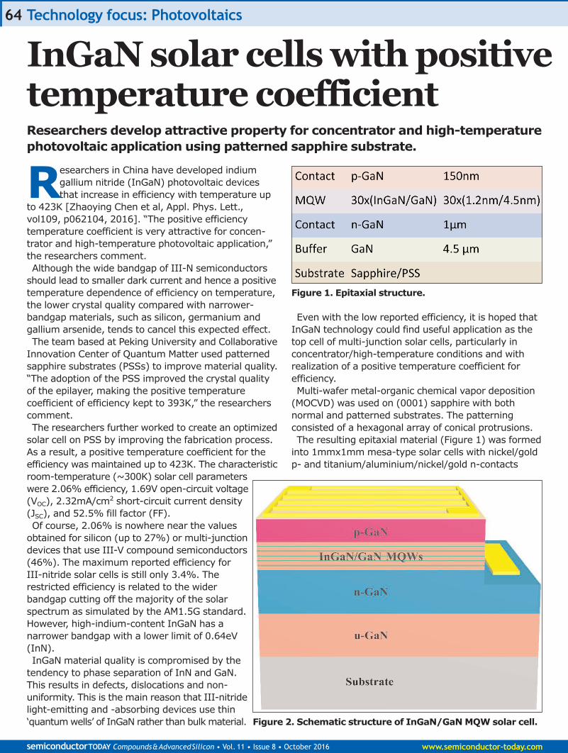
Researchers in China have developed indium gallium nitride (InGaN) photovoltaic devicesthat increase in efficiency with temperature up
to 423K [Zhaoying Chen et al, Appl. Phys. Lett.,vol109, p062104, 2016]. “The positive efficiency temperature coefficient is very attractive for concen-trator and high-temperature photovoltaic application,”the researchers comment.Although the wide bandgap of III-N semiconductors
should lead to smaller dark current and hence a positivetemperature dependence of efficiency on temperature,the lower crystal quality compared with narrower-bandgap materials, such as silicon, germanium andgallium arsenide, tends to cancel this expected effect. The team based at Peking University and Collaborative
Innovation Center of Quantum Matter used patternedsapphire substrates (PSSs) to improve material quality.“The adoption of the PSS improved the crystal qualityof the epilayer, making the positive temperature coefficient of efficiency kept to 393K,” the researcherscomment.The researchers further worked to create an optimized
solar cell on PSS by improving the fabrication process.As a result, a positive temperature coefficient for theefficiency was maintained up to 423K. The characteristicroom-temperature (~300K) solar cell parameterswere 2.06% efficiency, 1.69V open-circuit voltage(VOC), 2.32mA/cm2 short-circuit current density(JSC), and 52.5% fill factor (FF).Of course, 2.06% is nowhere near the values
obtained for silicon (up to 27%) or multi-junctiondevices that use III-V compound semiconductors(46%). The maximum reported efficiency forIII-nitride solar cells is still only 3.4%. Therestricted efficiency is related to the widerbandgap cutting off the majority of the solarspectrum as simulated by the AM1.5G standard.However, high-indium-content InGaN has a narrower bandgap with a lower limit of 0.64eV(InN).InGaN material quality is compromised by the
tendency to phase separation of InN and GaN.This results in defects, dislocations and non-uniformity. This is the main reason that III-nitridelight-emitting and -absorbing devices use thin‘quantum wells’ of InGaN rather than bulk material.
Even with the low reported efficiency, it is hoped thatInGaN technology could find useful application as thetop cell of multi-junction solar cells, particularly in concentrator/high-temperature conditions and withrealization of a positive temperature coefficient for efficiency.Multi-wafer metal-organic chemical vapor deposition
(MOCVD) was used on (0001) sapphire with both normal and patterned substrates. The patterning consisted of a hexagonal array of conical protrusions. The resulting epitaxial material (Figure 1) was formed
into 1mmx1mm mesa-type solar cells with nickel/goldp- and titanium/aluminium/nickel/gold n-contacts
Technology focus: Photovoltaics 64
Figure 2. Schematic structure of InGaN/GaN MQW solar cell.
semiconductorTODAY Compounds&AdvancedSilicon • Vol. 11 • Issue 8 • October 2016 www.semiconductor-today.com
InGaN solar cells with positivetemperature coefficientResearchers develop attractive property for concentrator and high-temperaturephotovoltaic application using patterned sapphire substrate.
Figure 1. Epitaxial structure.

Technology focus: Photovoltaics
www.semiconductor-today.com semiconductorTODAY Compounds&AdvancedSilicon • Vol. 11 • Issue 8 • October 2016
65
(Figure 2). The p-contact was patterned in a grid with30nm/150nm layers and transparent conducting electrodes with 5nm/5nm layers.Photoluminescence and x-ray analysis suggested that
the InGaN quantum wells contained ~30% indiumfraction and were ~1.2nm thick. The GaN barrierswere around 4.5nm. Using patterned sapphire substrates reduced edge-type dislocation densities to 1.54x10⁸/cm2, compared with 4.07x10⁸/cm2 forplain sapphire. By contrast, screw-type dislocationsincreased slightly with patterning to 1.58x10⁸/cm2,compared with 1.34x10⁸/cm2 on plain sapphire.Patterning improved the photovoltaic efficiency by
23.4% (Table 1). The researchers attribute this to thedecrease in non-radiative recombination at dislocations,the resulting longer minority carrier lifetime increasingextraction into the photocurrent, and enhanced lightabsorption by the patterned sapphire texture.The cells on patterned sapphire also showed
increased efficiency with increased temperature up to
393K (Figure 3). By contrast, the device on plain sapphire showed a rapid decrease in efficiency.The short-circuit current increased with temperature
at almost the same rate in both devices. The teamrelates this to the narrowing of the InGaN bandgapwith temperature, resulting in the cell being able toconvert longer-wavelength photons. The narrowerbandgap also reduces the open-circuit voltage, but on plain sapphire the voltage is further degraded bydark current from non-radiative recombination. ■http://dx.doi.org/10.1063/1.4960765Author: Mike Cooke
Figure 3. Normalized temperature-dependent conversion efficiency (a), short-circuit current density (b),open-circuit voltage (c) and fill factor (d) for solar cells on PSS and sapphire.
Substrate VOC JSC FF Efficiency
PSS 2.01V 0.97mA/cm2 59.4% 1.16%Sapphire 2.06V 0.71mA/cm2 64.4% 0.94%
Table 1. Summary of solar cell performance ofsamples on sapphire and PSS.
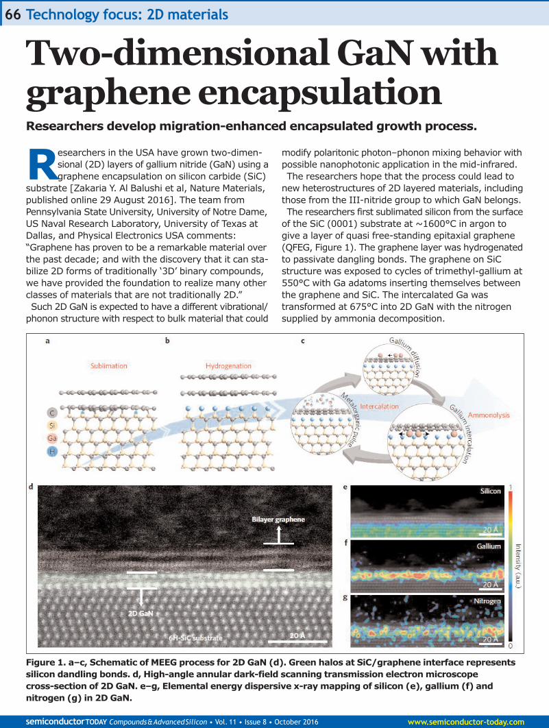
Researchers in the USA have grown two-dimen-sional (2D) layers of gallium nitride (GaN) using agraphene encapsulation on silicon carbide (SiC)
substrate [Zakaria Y. Al Balushi et al, Nature Materials,published online 29 August 2016]. The team fromPennsylvania State University, University of Notre Dame,US Naval Research Laboratory, University of Texas atDallas, and Physical Electronics USA comments:“Graphene has proven to be a remarkable material overthe past decade; and with the discovery that it can sta-bilize 2D forms of traditionally ‘3D’ binary compounds,we have provided the foundation to realize many otherclasses of materials that are not traditionally 2D.” Such 2D GaN is expected to have a different vibrational/
phonon structure with respect to bulk material that could
modify polaritonic photon–phonon mixing behavior withpossible nanophotonic application in the mid-infrared. The researchers hope that the process could lead to
new heterostructures of 2D layered materials, includingthose from the III-nitride group to which GaN belongs.The researchers first sublimated silicon from the surface
of the SiC (0001) substrate at ~1600°C in argon togive a layer of quasi free-standing epitaxial graphene(QFEG, Figure 1). The graphene layer was hydrogenatedto passivate dangling bonds. The graphene on SiCstructure was exposed to cycles of trimethyl-gallium at550°C with Ga adatoms inserting themselves betweenthe graphene and SiC. The intercalated Ga was transformed at 675°C into 2D GaN with the nitrogensupplied by ammonia decomposition.
Technology focus: 2D materials 66
Figure 1. a–c, Schematic of MEEG process for 2D GaN (d). Green halos at SiC/graphene interface representssilicon dandling bonds. d, High-angle annular dark-field scanning transmission electron microscope cross-section of 2D GaN. e–g, Elemental energy dispersive x-ray mapping of silicon (e), gallium (f) andnitrogen (g) in 2D GaN.
semiconductorTODAY Compounds&AdvancedSilicon • Vol. 11 • Issue 8 • October 2016 www.semiconductor-today.com
Two-dimensional GaN withgraphene encapsulationResearchers develop migration-enhanced encapsulated growth process.

Technology focus: 2D materials
www.semiconductor-today.com semiconductorTODAY Compounds&AdvancedSilicon • Vol. 11 • Issue 8 • October 2016
67
It was found that the “migration-enhanced encapsulated growth”(MEEG) process resulted in two layersof GaN encapsulated by a bilayer ofgraphene. Examination of the sampleshowed that the intercalation was facili-tated by defects of the graphene struc-ture (point-, wrinkles, metal-grapheneinteractions). The MEEG process alsocauses increased defects in thegraphene over regions of 2D GaN.The researchers also used the MEEG
process to produce thicker, more-than-5nm layers of 2D GaN. The surface ter-mination of the 2D GaN was similar tothat found with the two-layer GaN.Ultraviolet–visible reflectance meas-
urements found an inflection point at4.90eV, not observed in samples with-out GaN (Figure 2). The researcherstherefore believe that 4.90eV representsthe region of the bandgap energy (Eg)of the 2D GaN. Density functional theory(DFT) calculations predict values of4.79eV and 4.89eV, according to differ-ent approximations. Another approachusing absorption coefficients in theultraviolet–visible range gave a directbandgap of 4.98±0.13eV. These valuesare much higher than the 3.42eV ofnormal bulk GaN.The researchers also used low-loss
electron energy-loss spectroscopy(EELS) measurements on material withthe graphene encapsulation removed,resulting in a 5.53eV bandgap. Theteam comments: “The ~0.6eV deviationin the Eg measured from low-loss EELSarises from specular losses, such asCerenkov loss, that are observed inEELS measurements of high-dielectricmaterials. Our results, however, providedirect evidence that the Eg is muchlarger than that found in bulk GaN, withtheoretical and experimental valuesbeing in good agreement.”Vertical current flow was also measured
using conductive atomic force microscopy(AFM). Forward bias flow is believed tobe mainly electrons pulled from the accumulated n-type6H-SiC over a ~1.7V conduction band offset betweenSiC and 2D GaN. The reverse flow is tentatively attributedto “electron injection from graphene over the Schottkybarrier provided by 2D GaN, and into the depleted n-type 6H-SiC”. Away from the regions of 2D GaN theconduction was ohmic (i.e. approximately linear).
Analysis suggests the 2D GaN regions were in a buckled state and the stoichiometric composition wasnot 1:1. The layer was covalently bonded with theunderlying SiC; the bonding with the graphene encap-sulation was van der Waals. ■http://dx.doi.org/10.1038/nmat4742Author: Mike Cooke
Figure 2. a, Absorption coefficient (α) of 2D GaN fromultraviolet–visible spectroscopic ellipsometry, revealing direct Eg of4.98 eV. Connecting line is to guide eye. b, Vertical transportmeasurements with 2D GaN Schottky barrier. Current–voltage curveof heterostructure (green) and QFEG/6H-SiC (red curve in top-leftinset) collected with conductive AFM (bottom-right schematic).
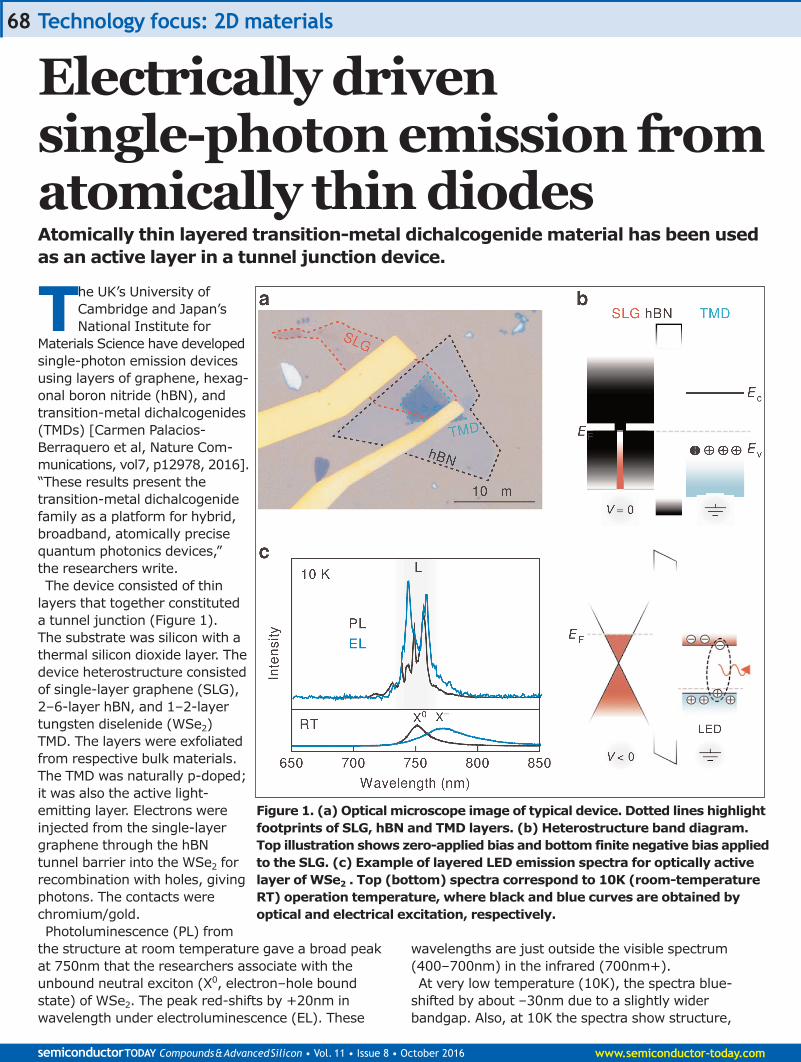
The UK’s University of Cambridge and Japan’sNational Institute for
Materials Science have developedsingle-photon emission devicesusing layers of graphene, hexag-onal boron nitride (hBN), andtransition-metal dichalcogenides(TMDs) [Carmen Palacios-Berraquero et al, Nature Com-munications, vol7, p12978, 2016].“These results present the transition-metal dichalcogenidefamily as a platform for hybrid,broadband, atomically precisequantum photonics devices,” the researchers write.The device consisted of thin
layers that together constituteda tunnel junction (Figure 1). The substrate was silicon with athermal silicon dioxide layer. Thedevice heterostructure consistedof single-layer graphene (SLG),2–6-layer hBN, and 1–2-layertungsten diselenide (WSe2)TMD. The layers were exfoliatedfrom respective bulk materials.The TMD was naturally p-doped;it was also the active light-emitting layer. Electrons wereinjected from the single-layergraphene through the hBN tunnel barrier into the WSe2 forrecombination with holes, givingphotons. The contacts werechromium/gold. Photoluminescence (PL) from
the structure at room temperature gave a broad peakat 750nm that the researchers associate with theunbound neutral exciton (X0, electron–hole boundstate) of WSe2. The peak red-shifts by +20nm inwavelength under electroluminescence (EL). These
wavelengths are just outside the visible spectrum(400–700nm) in the infrared (700nm+).At very low temperature (10K), the spectra blue-
shifted by about –30nm due to a slightly widerbandgap. Also, at 10K the spectra show structure,
Technology focus: 2D materials 68
Figure 1. (a) Optical microscope image of typical device. Dotted lines highlightfootprints of SLG, hBN and TMD layers. (b) Heterostructure band diagram. Top illustration shows zero-applied bias and bottom finite negative bias appliedto the SLG. (c) Example of layered LED emission spectra for optically activelayer of WSe2 . Top (bottom) spectra correspond to 10K (room-temperatureRT) operation temperature, where black and blue curves are obtained byoptical and electrical excitation, respectively.
semiconductorTODAY Compounds&AdvancedSilicon • Vol. 11 • Issue 8 • October 2016 www.semiconductor-today.com
Electrically driven single-photon emission fromatomically thin diodesAtomically thin layered transition-metal dichalcogenide material has been usedas an active layer in a tunnel junction device.
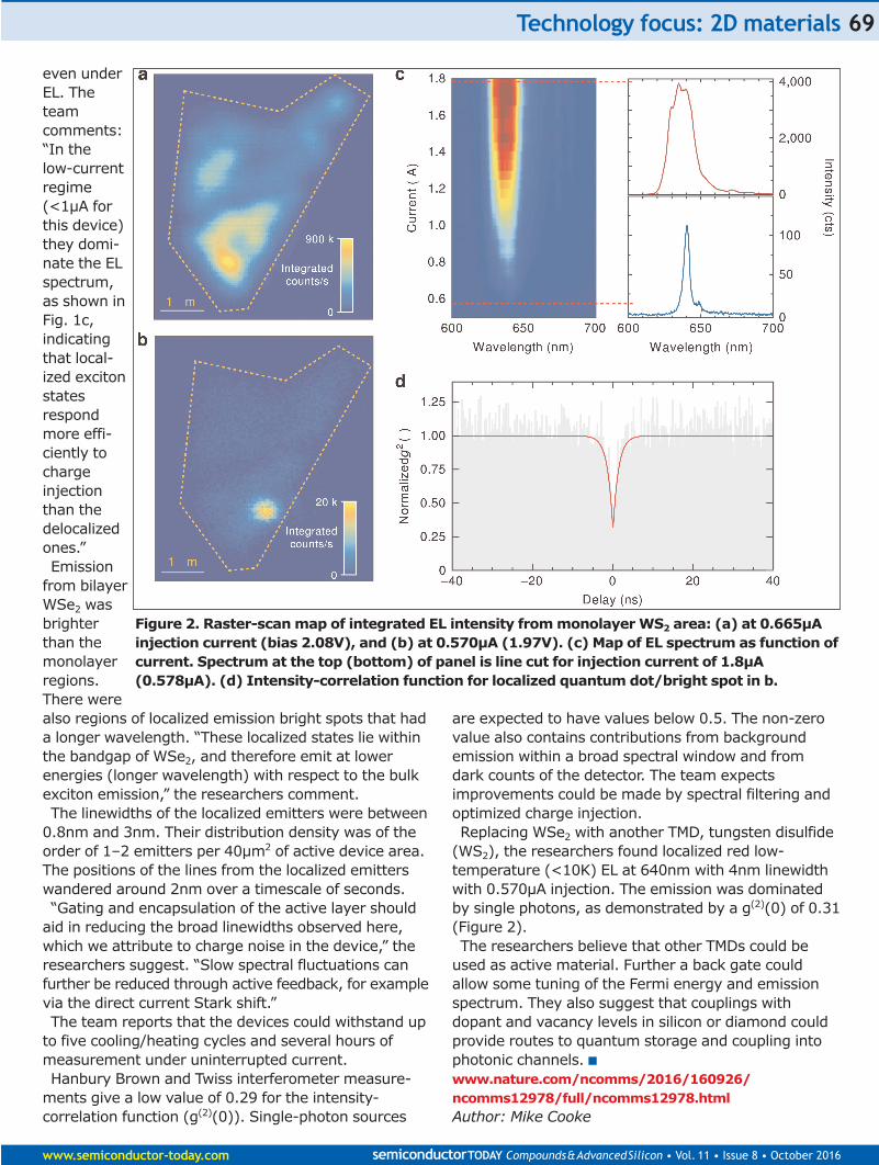
Technology focus: 2D materials
www.semiconductor-today.com semiconductorTODAY Compounds&AdvancedSilicon • Vol. 11 • Issue 8 • October 2016
69
even underEL. Theteam comments:“In the low-currentregime(<1µA forthis device)they domi-nate the ELspectrum,as shown inFig. 1c,indicatingthat local-ized excitonstatesrespondmore effi-ciently tochargeinjectionthan thedelocalizedones.”Emission
from bilayerWSe2 wasbrighterthan themonolayerregions.There werealso regions of localized emission bright spots that hada longer wavelength. “These localized states lie withinthe bandgap of WSe2, and therefore emit at lowerenergies (longer wavelength) with respect to the bulkexciton emission,” the researchers comment.The linewidths of the localized emitters were between
0.8nm and 3nm. Their distribution density was of theorder of 1–2 emitters per 40µm2 of active device area.The positions of the lines from the localized emitterswandered around 2nm over a timescale of seconds.“Gating and encapsulation of the active layer should
aid in reducing the broad linewidths observed here,which we attribute to charge noise in the device,” theresearchers suggest. “Slow spectral fluctuations canfurther be reduced through active feedback, for examplevia the direct current Stark shift.”The team reports that the devices could withstand up
to five cooling/heating cycles and several hours ofmeasurement under uninterrupted current.Hanbury Brown and Twiss interferometer measure-
ments give a low value of 0.29 for the intensity-correlation function (g(2)(0)). Single-photon sources
are expected to have values below 0.5. The non-zerovalue also contains contributions from backgroundemission within a broad spectral window and from dark counts of the detector. The team expectsimprovements could be made by spectral filtering andoptimized charge injection. Replacing WSe2 with another TMD, tungsten disulfide
(WS2), the researchers found localized red low-temperature (<10K) EL at 640nm with 4nm linewidthwith 0.570µA injection. The emission was dominatedby single photons, as demonstrated by a g(2)(0) of 0.31(Figure 2).The researchers believe that other TMDs could be
used as active material. Further a back gate couldallow some tuning of the Fermi energy and emissionspectrum. They also suggest that couplings withdopant and vacancy levels in silicon or diamond couldprovide routes to quantum storage and coupling intophotonic channels. ■www.nature.com/ncomms/2016/160926/ncomms12978/full/ncomms12978.htmlAuthor: Mike Cooke
Figure 2. Raster-scan map of integrated EL intensity from monolayer WS2 area: (a) at 0.665µAinjection current (bias 2.08V), and (b) at 0.570µA (1.97V). (c) Map of EL spectrum as function ofcurrent. Spectrum at the top (bottom) of panel is line cut for injection current of 1.8µA(0.578µA). (d) Intensity-correlation function for localized quantum dot/bright spot in b.
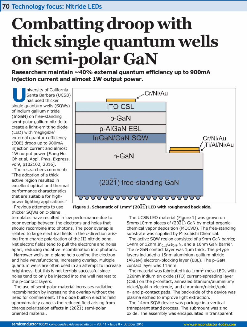
University of CaliforniaSanta Barbara (UCSB)has used thicker
single quantum wells (SQWs)of indium gallium nitride(InGaN) on free-standingsemi-polar gallium nitride tocreate a light-emitting diode(LED) with ‘negligible’ external quantum efficiency(EQE) droop up to 900mAinjection current and almost1W output power [Sang HoOh et al, Appl. Phys. Express,vol9, p102102, 2016].The researchers comment:
“The adoption of a thickactive region resulted inexcellent optical and thermalperformance characteristicsthat are suitable for high-power lighting applications.”Previous attempts to use
thicker SQWs on c-planetemplates have resulted in low performance due topoor overlap between the electrons and holes thatshould recombine into photons. The poor overlap isrelated to large electrical fields in the c-direction aris-ing from charge polarization of the III-nitride bond.Net electric fields tend to pull the electrons and holesapart, reducing radiative recombination into photons.Narrower wells on c-plane help confine the electron
and hole wavefunctions, increasing overlap. Multiplequantum wells are often used in an attempt to increasebrightness, but this is not terribly successful sinceholes tend to only be injected into the well nearest tothe p-contact layers.The use of semi-polar material increases radiative
recombination by increasing the overlap without theneed for confinement. The diode built-in electric fieldapproximately cancels the reduced field arising fromcharge polarization effects in (2021) semi-polar oriented material.
The UCSB LED material (Figure 1) was grown on5mmx10mm pieces of (2021) GaN by metal-organicchemical vapor deposition (MOCVD). The free-standingsubstrate was supplied by Mitsubishi Chemical.The active SQW region consisted of a 9nm GaN barrier,
14nm or 12nm In0.16Ga0.84N, and a 16nm GaN barrier.The n-GaN contact layer was 1µm thick. The p-typelayers included a 15nm aluminium gallium nitride(AlGaN) electron-blocking layer (EBL). The p-GaN contact layer was 115nm.The material was fabricated into 1mm2-mesa LEDs with
220nm indium tin oxide (ITO) current-spreading layer(CSL) on the p-contact, annealed titanium/aluminium/nickel/gold n-electrode, and chromium/nickel/gold n- and p-contact pads. The back-side of the device wasplasma etched to improve light extraction.The 14nm SQW device was package in a vertical
transparent stand process. The submount was zincoxide. The assembly was encapsulated in transparent
Technology focus: Nitride LEDs 70
Figure 1. Schematic of 1mm2 (2021) LED with roughened back side.
semiconductorTODAY Compounds&AdvancedSilicon • Vol. 11 • Issue 8 • October 2016 www.semiconductor-today.com
Combatting droop with thick single quantum wellson semi-polar GaNResearchers maintain ~40% external quantum efficiency up to 900mAinjection current and almost 1W output power.
––
––
––

Technology focus: Nitride LEDs
www.semiconductor-today.com semiconductorTODAY Compounds&AdvancedSilicon • Vol. 11 • Issue 8 • October 2016
71
silicone with 1.41 refractive index. The 12nm SQW LEDwas mounted on a heating stage without encapsu-lation. The output power and external quantum efficiency of
the 14nm SQW LED showed much improved perform-ance with respect to current (Table 1). The peak EQEof 42.3% occurred at 200mA. The peak EQE was onlyslightly lower than for a previous smaller-area(0.1mm2) device. The difference is explained as beingdue to reduced light-extraction efficiency and current-crowding effects of larger-area LEDs. However, at900mA current injection the device shows ‘negligible’efficiency droop, which the researchers attribute to thelower carrier density allowed by the thick SQW.While the EQE (photons/electron) is approximately
flat above the peak, the wall-plug efficiency (WPE, output/input power) declines due to an increase in for-ward voltage. The researchers comment: “The forwardvoltage at 200mA (20A/cm2) is 3.6V, which is relativelyhigh compared with those of commercial LEDs, andresults in a reduction in WPE at drive currents. Furtheroptimization of the resistance of the p-contacts, n-contacts, ITO current-spreading layers, and n-GaN current-spreading layers should reduce the forward voltage andincrease the WPE ofthe LEDs.”The 12nm SQW
LED was used intemperature char-acterization. Thedemonstrated EQEwas less than 15%.This was due to thehorizontal orienta-tion and absence ofencapsulation,according to theteam. Increasingthe temperaturereduced the EQE,but did not add anyefficiency droop,which was small atall temperatures upto 100°C. Thehot/cold factor ofEQE at 100°C/20°Cwas constant ataround 0.9 for currents between100mA and 900mA(0.92 factor). Thecharacteristic temperature for theoutput power droop
was more than 800K (884K at 900mA).The researchers maintain that these results indicate
thermionic escape had an insignificant effect on droop.“This indicates that carrier leakage due to thethermionic escape is unlikely to be a cause of the efficiency droop,” they add.The researchers also found that the temperature
dependence was similar to that of small-area 0.1mm2
devices. They conclude that the new devices are “well suited for high-power solid-state lighting appli-cations that require thermal stability”. ■http://doi.org/10.7567/APEX.9.102102Author: Mike Cooke
Figure 2. (a) Dependence of hot/cold factor on current for (2021) blue LED with 12nmSQW. (b) Dependence of characteristic temperature on current for same LED (T = 100°C).
Current Output power EQE
100mA 112mW 40.1%200mA 236mW 42.3%500mA 574mW 41.1%900mA 991mW 39.4%
Table 1. Output power and EQE at differentcurrent injection levels for (2021) blue LED with14nm SQW.
––
––
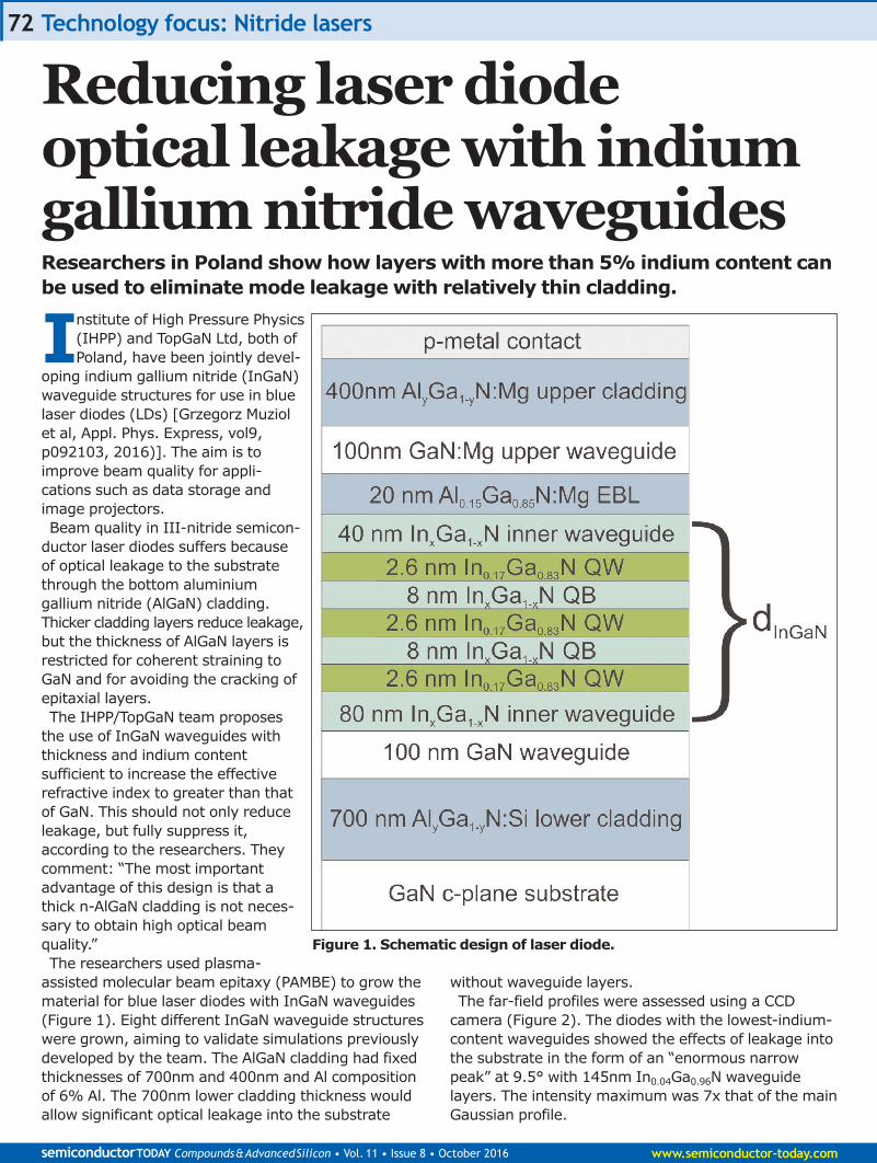
Institute of High Pressure Physics(IHPP) and TopGaN Ltd, both ofPoland, have been jointly devel-
oping indium gallium nitride (InGaN)waveguide structures for use in bluelaser diodes (LDs) [Grzegorz Muziolet al, Appl. Phys. Express, vol9,p092103, 2016)]. The aim is toimprove beam quality for appli-cations such as data storage andimage projectors.Beam quality in III-nitride semicon-
ductor laser diodes suffers becauseof optical leakage to the substratethrough the bottom aluminium gallium nitride (AlGaN) cladding.Thicker cladding layers reduce leakage,but the thickness of AlGaN layers isrestricted for coherent straining toGaN and for avoiding the cracking ofepitaxial layers. The IHPP/TopGaN team proposes
the use of InGaN waveguides withthickness and indium content sufficient to increase the effectiverefractive index to greater than thatof GaN. This should not only reduceleakage, but fully suppress it, according to the researchers. Theycomment: “The most importantadvantage of this design is that athick n-AlGaN cladding is not neces-sary to obtain high optical beamquality.” The researchers used plasma-
assisted molecular beam epitaxy (PAMBE) to grow thematerial for blue laser diodes with InGaN waveguides(Figure 1). Eight different InGaN waveguide structureswere grown, aiming to validate simulations previouslydeveloped by the team. The AlGaN cladding had fixedthicknesses of 700nm and 400nm and Al compositionof 6% Al. The 700nm lower cladding thickness wouldallow significant optical leakage into the substrate
without waveguide layers.The far-field profiles were assessed using a CCD
camera (Figure 2). The diodes with the lowest-indium-content waveguides showed the effects of leakage intothe substrate in the form of an “enormous narrowpeak” at 9.5° with 145nm In0.04Ga0.96N waveguide layers. The intensity maximum was 7x that of the mainGaussian profile.
Technology focus: Nitride lasers 72
semiconductorTODAY Compounds&AdvancedSilicon • Vol. 11 • Issue 8 • October 2016 www.semiconductor-today.com
Reducing laser diode optical leakage with indiumgallium nitride waveguides
Figure 1. Schematic design of laser diode.
Researchers in Poland show how layers with more than 5% indium content canbe used to eliminate mode leakage with relatively thin cladding.

Technology focus: Nitride lasers
www.semiconductor-today.com semiconductorTODAY Compounds&AdvancedSilicon • Vol. 11 • Issue 8 • October 2016
73
The researchers comment: “This is amanifestation of astrong leakage to theGaN substrate. It is sostrongly pronouncedbecause the thicknessof the n-AlGaN claddinglayer is insufficient toreduce it. If the thick-ness would be higher,the leakage and thusthe magnitude of thepeak could be reduced.The amount of light inthis peak is 25% of theoverall far-field patternand agrees well withthe value of 21% predicted theoretically.”The width and height
of the measured peak isbroader and shorterthan the simulations,however. The team suggests that this could be due to smallinhomogeneities ofelectron concentration,affecting the refractiveindex.The InGaN wave-
guides with indium con-tent higher than 5%had no visible leakagepeaks, in line with themodeling. ■http://doi.org/10.7567/APEX.9.092103 Author: Mike Cooke
Figure 2.Experimentallymeasured fast axis oflaser diode far-fieldpatterns with variousInGaN waveguidecompositions andthicknesses.
Register for Semiconductor Today free at www.semiconductor-today.com

Oracle Networking Group in the USA believesthat it has made the first demonstration of anintegrated surface-normal coupled laser array
on a silicon-on-insulator photonics platform [Shiyun Linet al, Optics Express, vol24, p21455, 2016]. Passively aligned (i.e. laser off) high-accuracy flip-chip
bonding was used to combine a III-V reflective semiconductor optical amplifier (RSOA) array withintegrated total internal reflection mirrors onto CMOSsilicon-on-insulator (SOI) containing silicon photoniccircuits (Figure 1). The completed assembly formed atunable hybrid external-cavity laser array.The aim of the work is to fill the gap in silicon photonics
for high-efficiency laser sources, giving a completeplatform for next-generation optical interconnects thatneed large bandwidth, high density and high powerefficiency.The 2mmx2mm RSOA chip contained multiple quan-
tum wells on indium phosphide (InP) with 600µm-longridge waveguides in a 2x6 array. The pitch of the arraywas 1mm along the waveguide and 250µm perpendi-cular to this direction.Chemically assisted ion-beam etch was used to
create an angled mirror-facet. The light from the total-internal reflection mirror was angled to match the
grating couplers (GCs) in the silicon photonics circuit. A further mirror on the back-facet of the RSOA wascoated with material to give more than 95% reflectivity.The chip’s top surface was coated with anti-reflectivematerial to reduce back reflection. The silicon photonic circuit was fabricated using a
silicon-on-insulator substrate with 300nm of silicon on0.8µm of buried oxide. A 130nm CMOS process wasused to create a 2x6 array of ring reflector circuits thatmatched the RSOA chip (Figure 2). Silicon resistormicro-heaters were incorporated into the rings to provide laser wavelength tuning. Grating couplers wereused to couple light into and out of the circuit. The lightwas output into a fiber array.CMOS aluminium metalization provided bonding pads
for the RSOA and metal traces to large probing pads.Under-bump metalization consisted of titanium-gold.Gold-tin (AuSn) bumps were sputtered onto the CMOS pads.The one-step passive bonding process had a peak
temperature of 320°C. The RSOA and SOI chips werebonded using a high-accuracy flip-chip bonder with analignment tolerance of ±0.5µm. The alignment wasachieved in a one-step passive process with matchingpatterns near the coupling region. The demonstration
Technology focus: III-Vs on silicon 74
Figure 1. (a) Side-view schematic of surface-normal coupled hybrid laser, (b) microscope image of integrated2x6 hybrid external-cavity laser array.
semiconductorTODAY Compounds&AdvancedSilicon • Vol. 11 • Issue 8 • October 2016 www.semiconductor-today.com
Researchers claim first demonstration of an integrated surface-normal coupledlaser array on a silicon-on-insulator photonics platform.
Flip-chip hybrid external-cavity laser array on silicon platform

Technology focus: III-Vs on silicon
www.semiconductor-today.com semiconductorTODAY Compounds&AdvancedSilicon • Vol. 11 • Issue 8 • October 2016
75
used chip-to-chip bonding, but the researchers believethat the technique could be expanded to a wafer-scalepick-and-place set up. Indeed the automated bondingmachine is designed for wafer-scale operation.The maximum waveguide-coupled wall-plug efficiency
(wcWPE) was 2%. The maximum optical power wasgreater than 3mW. The researchers described the efficiency as “relatively low” due to a large couplingloss between the RSOA and SOI chips. The researchersattribute this to a ~3dB coupling loss from the modesize mismatch between the III-V and the GC. Themode-field diameter of the RSOA was 1.3µm in thevertical direction and 2.0µm in the horizontal direction.The GCs had a diameter of 4µm in both directions.Also, there is a 14µm gap between III-V waveguideand GC that increases the coupling loss to 7dB.Increasing the III-V mode-field diameter to 3µmx3µmwould reduce the coupling loss by ~3dB. With the laser drive current at 80mA, the tunability
range by heating was 1544–1556nm. The devicestopped lasing outside this window. Reducing the outputpower ratio increased the range from 12nm to 19nm.The cross-coupling ratio was designed to be 50% forthe top row of lasers in the RSOA and 25% in the bottom row. The tuning efficiency of both rows was0.2nm/mW. The researchers believe this can beimproved by localized substrate removal.The team comments: “In order to improve the
wcWPE, a smaller gap between III-V waveguide andsilicon GC is desirable, and can be achieved by bringingthe top metal closer to the InP layer and removing theunnecessary metal/dielectric layer stacks on the SOIchip. Together with a larger mode size, we believe acoupling loss of less than 3dB is achievable.”The researchers attempted to work towards improved
wcWPE by fabricating a 1x6 array SOI chip with only asingle metal layer rather than the full metal/dielectricstacking to reduce the gap between the componentdevices. A 2x6 RSOA was bonded onto the new SOIchip. The coupling ratio of the directional couplers was50%. Platinum heaters were used for tuning. Thesefactors reduced the gap to 10µm. The researchers esti-mated that this improved the optical coupling by 2dB.“The gap can be further reduced by optimizing thecontact design on the RSOA chip and reducing thethickness of the AuSn bumps,” the team writes.Unfortunately, two of the channels of the new assembly
were damaged in post-processing, leaving a 1x4 arrayof working lasers. The output power was ~10mW at120mA drive current. The wcWPE was calculated at 5%.The team believes that a high-efficiency laser arraycould be achieved by further reducing the coupling lossby using a mode size converter on the RSOA chip togive a larger mode size. ■http://dx.doi.org/10.1364/OE.24.021454Author: Mike Cooke
Figure 2. (a) Microscope image of CMOS SOI chip with 2x6 ring reflector circuit array, (b) schematic diagramof ring reflector design.
REGISTERfor Semiconductor Today
free at www.semiconductor-today.com

In the past year or so, new optical communicationstechnologies for data communications and high-speed computer processing have become
available based on silicon (Si) waveguides [See MikeCooke, Semiconductor Today, p80, September 2016].Silicon provides a versatile platform for both optics andelectronics, but suffers from major limitations in termsof generating light, which must either be suppliedexternally or created internally using III-V compoundsemiconductor materials.Combining III–V materials with silicon is tricky, and
germanium (Ge) is often used as a bridge. As a group IVmaterial, Ge shares many chemical properties with Si andis already used in mainstream electronics production.Here we look at some ways for how Ge could help tomake possible more integrated optoelectronics on asilicon platform.
Silicon germanium LEDsChina’s Xiamen and Nankai universities have jointlydeveloped lateral p-i-n SiGe/Ge/SiGe light-emittingdiodes (LEDs) with high luminous extraction comparedwith a vertical design [Guangyang Lin et al, Appl. Phys.Lett., vol109, p141104, 2016].An efficient Ge-based light-emitting device is highly
desired as part of the drive to silicon-based optoelec-tronic integrated circuits. Since Ge has a narrowerbandgap than Si (Table 1), generated light could beused in silicon photonic structures that require wave-lengths longer than 1.1μm.The impediment to using Ge in this way is its
indirect bandgap, which makes for very inefficient electron–hole recombination into photons. However,the difference between the indirect minimum anddirect transitions between the conduction and valencebands is only about 140meV, giving a ‘quasi-direct’ gap.This difference can be further reduced by applying tensile strain. On the processing side, Ge is already used in many
mainstream electronics enhancements such as‘strained silicon’ transistors and in SiGe bipolar transis-tors. This is in contrast to standard direct-bandgaplight-emitting III–V compound semiconductors made
of materials that poison the performance of standardSi components. Some vertical LEDs using various SiGe combinations
have been developed. The Xiamen/Nankai researchersbelieve that lateral junctions could be a better choice interms of reducing carrier loss in defect-rich Ge bufferlayers at the Ge/Si interface, light absorption in metalcontacts, and self-absorption in Ge. “So far, few workswere reported on Ge lateral junction light emissiondiodes, especially with lateral heterojunctions,” theywrite. The Xiamen/Nankai epitaxial structure was grown on
a Ge ‘virtual substrate’ (VS) on silicon on insulator (SOI).Six 9nm Ge quantum wells were separated by 15nmSi0.13Ge0.87 barriers. The structure was annealed at800ºC for 60 seconds, intermixing the 6x(SiGe/Ge)structure to give a uniform SiGe layer. Raman analysissuggests the resulting 159nm layer consisted of 95%Ge with ~1% strain. The strain in the underlying Gewas ~0.3%.The researchers comment that the high annealing
temperature of 800ºC enhanced the tensile strain dueto differences in thermal expansion coefficients betweenSi and Ge. “The tensile-strained SiGe overlayer canalso act as an external strain source leading to largertensile strain in the Ge VS, which is beneficial forachievement of direct band luminescence from Ge,”they add.Fabrication (Figure 1) included dry etching down to
the buried oxide insulator layer to give 10μm-widewaveguides, dry etching the SiGe layer to form a lateraldouble heterojunction (SiGe/Ge/SiGe), ion implantationto form p- and n-type SiGe contacts, doping activation
Technical focus: III-Vs on silicon — optoelectronics
semiconductorTODAY Compounds&AdvancedSilicon • Vol. 11 • Issue 8 • October 2016 www.semiconductor-today.com
76
Si Ge
Bandgap 1.12eV 0.661eVWavelength 1.1μm 1.9μmSeparation at gamma point (k = 0, peak valence band) 3.4eV 0.8eVElectron effective mass/vacuum mass 0.33 0.2Hole effective mass/vacuum mass 0.5 0.3
Table 1. Silicon versus germanium.
Mike Cooke reports on recent research using germanium to enable infrared light-emitting devices to be created on silicon platforms.
Germanium and silicon photonics

at 650ºC for 15 seconds, encapsulation in silicon dioxide,formation of contact holes and deposition and pattern-ing of aluminium electrodes and wiring. The team saysthat the fabrication process is CMOS-compatible,paving the way for integration with Ge MOSFETs.Vertical p-i-n Ge homojunction devices were also
fabricated on SOI with a similar area for comparison.As current injection in the lateral device was increased,
electroluminescence (EL) around 1600nm (1.6μm)wavelength was detected by an indium gallium arsenide(InGaAs) on indium phosphide (InP) photodetector(Figure 2). Red-shift was seen at higher currents dueto Joule heating. At 2.5kA/cm2 current injection, thepeak intensity for the lateral heterostructure devicewas 4x that of the vertical homojunction structure. “In addition, the EL peak position of the lateral hetero-junction locates at the higher energy side compared tothe vertical homojunction, which might be attributed tomodification of spectra by the cavity effect and/orweaker Joule heating effect,” the researchers write.The increase in intensity with current for 20μm- and
2μm-wide i-Ge region lateral devices is approximatelyquadratic (1.9 current-exponent for 20μm, 2.0 for 2μm),consistent with theoretical considerations of large carrier injection. The 20μm peak intensity is about 3xthat of the 2μm device.Light extraction from the device also benefits from
reflection off of the silicon dioxide/silicon interface ofthe SOI substrate, giving enhancement from a cavityresonance effect.
First 1.3μμm EL from MOCVD quantum dotsJapan’s University of Tokyo claims “the first demon-stration of EL at 1.3mm from InAs/GaAs quantum dots(QDs) monolithically grown on a Ge/Si substrate bymetal organic chemical vapor deposition (MOCVD)”[Mohan Rajesh et al, Jpn. J. Appl. Phys., vol55,p100304, 2016].The researchers see the room-temperature
achievement as an important milestone towards themonolithic integration of QD lasers emitting at 1.3μmfor silicon photonics application.QD lasers can have improved characteristics such as
low threshold current and high temperature stabilitycompared with more traditional devices based onquantum wells. Producing electrically pumped laserson silicon could plug the light generation gap in silicon photonics technologies. QD lasers have beenproduced through molecular beam epitaxy (MBE) onsilicon, but MOCVD is often a preferred mass-productiontechnology in terms of high throughput and low maintenance cost.The Tokyo InAs in GaAs matrix QD structures were
produced on a Ge interlayer on the Si substrate. III–Vmaterial such as GaAs tends to suffer from crystalimperfection when grown directly on silicon due to alarge 4.1% lattice mismatch. Germanium has asmaller mismatch with GaAs of the order of 0.07%.Also, the thermal expansion coefficients of Ge and GaAsare similar, which is an important factor when high-temperature growth processes are used.
Technical focus: III-Vs on silicon — optoelectronics
www.semiconductor-today.com semiconductorTODAY Compounds&AdvancedSilicon • Vol. 11 • Issue 8 • October 2016
77
Figure 1. Fabrication flow of lateral p-SiGe/i-Ge/n-SiGe heterojunctions on SOI substrates: (a) SiGe/Ge/Siwaveguides on SOI, (b) SiGe/Ge/SiGe lateral heterojunctions on waveguides, (c) selective ion implantationto form P+ and N+ SiGe regions, and (d) schematic of top view and cross sections.

The 2μm Ge interlayer was grown using ultra-high-vacuum CVD on a 6º-offcut silicon substrate. A further100nm of Ge was grown after 5 minutes of cyclicannealing at 850ºC. The Ge/Si wafer was prepared for III–V MOCVD by a series of treatments to removecontaminants and native oxide.When the Ge/Si wafer was loaded into the MOCVD
reactor a further treatment of thermal annealing in tertiarybutylarsine at 650ºC for 10 minutes was used
to desorb native oxide and create doubleatomic steps on the substrate surface,avoiding antiphase domains (APDs) inthe subsequent growth.The GaAs buffer layer consisted of
10nm nucleation on the As prelayer at420ºC, 250nm low-temperature 500ºCmaterial, and finally the main part at650ºC to give 1.3μm or 3μm total thickness. The lower-temperature layersused triethylgallium precursor, while the high-temperature final part usedtrimethylgallium. Before QD deposition,the GaAs/Ge/Si wafer was annealed intertiarybutylarsine. The QDs were grown in a series of layers
using antimony (Sb) as a surfactant. The Sb was irradiated onto the GaAs surface, after which the 3.8-monolayerInAs QD material was deposited at495ºC. The growth was then interruptedfor 80 seconds to allow the dots to form.The QD density was greater than4.3x1010/cm2. The base width and heightwere 36nm and 7nm, respectively. “Thedensity of QDs grown on GaAs/Ge/Sisubstrate is almost comparable to that ofQDs grown on a GaAs substrate, used forthe fabrication of low-threshold-currentlasers,” the team writes.The QD layer was capped with 500ºC
7nm In0.05Ga0.95As and 5nm GaAs. The purpose of the In0.05Ga0.95As layer wasto reduce strain and to red-shift the InAsQD emission wavelength to 1.3μm andlonger with a full-width at half-maximum(FWHM) of ~44meV. The QD layers werecompleted with 600ºC 30nm GaAs spacerfor the next QD layer. The antimony (Sb) surfactant-mediated
growth increases dot density and suppresses coalescence. With certaingrowth conditions it can also increasephotoluminescence (PL) intensity. Previous work on InAs/GaAs QD MOCVDon Ge substrates has resulted in lowdensities and coalescence of dots.
It was found that the GaAs buffer layer (BL) needed tobe annealed at 600ºC to give PL intensity comparablewith QDs grown on GaAs substrate. The researchers comment: “The lower PL intensity in
the case of QDs grown on a Ge/Si substrate may beattributed to the relaxation of charge carriers to non-radiative recombination centers, such as threadingdislocations and APDs, formed at the GaAs/Ge interfaceand propagating into the GaAs BL and reaching the
Technical focus: III-Vs on silicon — optoelectronics
semiconductorTODAY Compounds&AdvancedSilicon • Vol. 11 • Issue 8 • October 2016 www.semiconductor-today.com
78
Figure 2. (a) Typical current density-voltage characteristic ofheterojunction diode. Inset forward bias curve in log–log scalemarked with extracted ideality factors; (b) EL spectra under variousinjection current densities.

QD active region,thereby quenchingthe QD emissionefficiency. Wehave observedthat the post-growth thermalannealing of theGaAs buffer layerprior to thegrowth of QDscan be a simpleand effective toolfor improving theluminescenceefficiency of theQDs grown onGe/Si sub-strates.” The researchers
used these tech-niques to createlight-emittingdiodes with eight layers ofQDs (Figure 3).The n- and p-cladding layersconsisted of1.4μmAl0.4Ga0.6As.These layerswere grown atmore than 600ºC,which can degradeunderlying QDs inthe case of the p-type cladding.In particular, thehigh temperaturecan diffuse gallium into andindium out of thedots, shorteningthe wavelength ofemissions.The researchers comment: “The realization of
electroluminescence at 1.3μm on Ge/Si, which is notblue-shifted, is attributed to our improved growth conditions of the InAs/Sb:GaAs QDs in the active layer,particularly the Sb irradiation time, before the depositionof InAs, as InAs/Sb:GaAs QDs do not show any blue-shift upon annealing at temperatures as high as630ºC.” The structure was capped with 300nm p+-GaAs
contact. The contact metal electrodes were gold on
gold-germanium-nickel alloy. The electron currentinjection was lateral from the top side of the device toavoid added series resistance from the high-defect-density GaAs/Ge/Si interfaces.Under reverse bias the current was of the order
10–8A, suggesting a good rectifying pn junction. Electroluminescence turned on around +0.8V forwardbias (Figure 4). Series resistance was around 10Ω. The peak wavelength was 1.3μm with 54meV full-widthhalf-maximum.
Technical focus: III-Vs on silicon — optoelectronics
www.semiconductor-today.com semiconductorTODAY Compounds&AdvancedSilicon • Vol. 11 • Issue 8 • October 2016
79
Figure 3. (a) Schematic layer structure of InAs/GaAs QD LED grown on Ge/Si substrate. (b) Cross-sectional high-resolution scanning electron microscope image of fabricated device.

The researchers comment: “To the best of our knowl-edge, this is the first demonstration of EL at 1.3μmfrom III–V QDs directly grown on a Ge/Si substrate byMOCVD.” Below 80mA, the increase in intensity with current is
approximately linear. With further injection, the output
saturates around 130mA andthen falls back slightly due tothermal roll-over, non-radiativeAuger processes, etc.The output suffers from
imperfect facets because of non-parallel/non-vertical cleavagealong the [100] plane. “Thecombined effect of facet polishingand high-reflection coating onthe facets, apart from furtherimproving the uniformity of theQDs in the active region andreducing the defect density inthe buffer layer, could poten-tially lead to the realization of aQD laser on silicon by MOCVD,”the team believes.
InGaAs laser diode onexact GeResearchers in Russia havedeveloped an InGaAs quantum well laser diode (LD) on(001) Ge-on-Si virtual substratewithout offcut angle [V. Ya.Aleshkin et al, Appl. Phys. Lett.,vol109, p061111, 2016]. Continuous wave lasing withemission wavelength of 941nmwas possible at cryogenic temperatures of 77K. Room-temperature lasing at 992nmwavelength was restricted topulsed mode. The researchers hope that in
future they will be able toextend the wavelength into thegreater than 1.1μm (>1100nm)transparency range needed foruse in conjunction with siliconwaveguides. “It is assumed thatthe increase of the In content in the InGaAs QW with anappropriate correction of theQW width could be a possiblesolution,” the team writes.Normally III–V materials such
as InGaAs on (001)-oriented silicon are grown with a signifi-
cant offcut angle of 4–6º to avoid the formation ofantiphase boundaries (APBs), which is a problem forpolar materials deposited on non-polar substrates.However, offcut angles complicate integration with
silicon electronics and photonics. In addition, Ge buffersare often used to accommodate lattice mismatching of
Technical focus: III-Vs on silicon — optoelectronics
semiconductorTODAY Compounds&AdvancedSilicon • Vol. 11 • Issue 8 • October 2016 www.semiconductor-today.com
80
Figure 4. (a) EL spectra of device at room temperature at various injectioncurrents. Inset: current–voltage characteristics of diode. (b) Integrated ELintensity as function of injection current. Inset: infrared camera near-fieldimage of light emission from as-cleaved facet bar at 40mA.

III–V heterostructureswith Si, but Ge onoffcut Si is generallyof low quality. Finally,offcut substrates leadto difficulty whencleaving the finaldevices into laserbars to give high-quality mirror facets.The team from
Institute for Physicsof Microstructures of the Russian Academy of Sciences,Lobachevsky StateUniversity of NizhnyNovgorod, and FGUE‘Salut’ produced theirGe/Si virtual sub-strate by solid-sourcemolecular beam epitaxy. The n-Sisubstrate had a (001)crystal orientationwith offcut angle lessthan 0.5º. A two-step process was used, involvingdeposition of 50nm Ge at 275ºC and then the remainder at 600ºC. The thin-layer growth allowsstrain relaxation through misfit dislocations. The higher-temperature growth gives better crystal qualitymaterial in the thicker layer. Further improvement wasachieved with short-time cycle annealing. The annealingwas found to reduce threading dislocation densitiesfrom 3–4x10⁸/cm2 to ~107/cm2.The III–V (A3B5) epitaxy involved metal-organic
chemical vapor deposition (Table 2). In theinitial planarizing buffer, two aluminiumarsenide (AlAs) inserts were used toreduce GaAs–Ge interdiffusion and to filterout defects. The AlAs layer also reducedsurface roughness by a factor of two.There were some APBs present due to the
use of a substrate with near-zero offcutangle. The APB density in the buffer layerwas around 0.6/μm. After the whole struc-ture was grown the density was 0.3/μm.The researchers comment: “These valuesof the APB density are significantly smallerthan the typical ones obtained duringgrowth of polar materials on the exactlyoriented non-polar Si(001) substrates. We believe that the influence of the APBs isnot the main critical factor affecting theoptical properties of the grownA3B5/Ge/Si(001) structure.”
Laser diodes (Figure 5) were fabricated with theactive region 20μm wide, and 200μm-wide planarohmic contacts of gold-germanium-nickel-gold (n-type)and chromium gold (p-type). The substrate wasthinned to 80μm. The material was cleaved into2.7mm-long bars with mirror facets.Under electric current injection at 77K (Figure 6),
the 941nm-wavelength emission peak narrowed from30nm below threshold to less than 1nm above. Room-temperature (300K) 992nm emission was 95nm wide
Technical focus: III-Vs on silicon — optoelectronics
www.semiconductor-today.com semiconductorTODAY Compounds&AdvancedSilicon • Vol. 11 • Issue 8 • October 2016
81
Figure 5. Schematic view of laser diode with planar ohmic contacts.
Thickness (nm) Doping (/cm3) Remark
Si(001) substrate (upper part) . . . Virtual substrate
Ge ~1000 . . .AlAs/GaAs/AlAs 10/50/10 . . . Planarizing
bufferGaAs:Si 2500 2x10¹⁸ Main buffer and
n-contactAl0.3Ga0.7As:Si 1000 5x10¹⁷ Bottom
waveguide layerGaAs 340 . . . Active region with
multiple InGaAs QWsIn0.17Ga0.83As QW 10 . . .GaAs 50 . . .In0.17Ga0.83As QW 10 . . .GaAs 50 . . .In0.17Ga0.83As QW 10 . . .GaAs 170 . . .GaAs:C 170 3x10¹⁶
Al0.3Ga0.7As:C 1000 5x10¹⁷ Top waveguide layer
GaAs:C 500 2x10¹⁹ p-contact
Table 1. Parameters of A3B5/Ge/Si(001) laser structure.

Technical focus: III-Vs on silicon — optoelectronics
semiconductorTODAY Compounds&AdvancedSilicon • Vol. 11 • Issue 8 • October 2016 www.semiconductor-today.com
82
below threshold and narrowed to less than 1nm above.The threshold for lasing at 77K was 463A/cm2, low enoughfor continuous wave operation. At 300K, only pulsedoperation was possible with ~5.5kA/cm2 threshold. ■
The author Mike Cooke is a freelance technology journalistwho has worked in the semiconductor and advancedtechnology sectors since 1997.
Figure 6. (a) EL spectra at sub-threshold (dashed lines) and above threshold (solid lines). Black linescorrespond to 77K, red ones to room temperature. For 77K (300K), pumping current density for subthresholdspectra was approximately 370A/cm2 (3.7kA/cm2); and for above threshold spectra 550A/cm2 (5.6kA/cm2).(b) Power–current characteristics of the same laser diode.
REGISTERfor Semiconductor Today
free at www.semiconductor-today.com

Choose Semiconductor Today for . . .
MAGAZINE
Accurate and timely coverage of the compound semiconductor and advanced silicon industries
Published 10 times a year and delivered by e-mail and RSS feeds
Targeted 41,000+ international circulation
WEB SITE
Average of over 19,700 unique visitors to the site each month
Google-listed news source
Daily news updates and regular feature articles
E-BRIEF
Weekly round-up of key business and technical news
E-mail delivery to entire circulation
Banner and text marketing opportunities available
www.semiconductor-today.com
Follow us on Twitter: Semiconductor_T
Join our LinkedIn group: Semiconductor Today
semiconductorTODAYC O M P O U N D S & A D V A N C E D S I L I C O NVol.7 • Issue 2 • March/April 2012 www.semiconductor-today.com
Graphensic spun off •Emcore sells VCSEL range to Sumitomo Masimo buys Spire Semiconductor•Oclaro and Opnext merge
ISSN 1752-2935 (online)
Efficiency droop in nitride & phosphide LEDsFirst single-crystal gallium oxide FET
Efficiency droop in nitride & phosphide LEDsFirst single-crystal gallium oxide FET

Shandong University in China and University ofManchester in the UK have reported room-tem-perature thermal-evaporation silicon monoxide
(SiO) passivation for aluminium gallium nitride (AlGaN)barrier high-electron-mobility transistors (HEMTs)[Gengchang Zhu et al, Appl. Phys. Lett., vol109,p113503, 2016].The passivation reduced leakage currents and
increased breakdown voltages compared with unpas-sivated and silicon nitride (SiNx) passivated devices.The researchers comment: “Because of the good passivation effectiveness, no ion damage, simplepreparation technology, and low cost, the thermallyevaporated SiO is a promising candidate as a surfacepassivation for GaN-based HEMTs, especially for high-power and noise-sensitive applications.”The SiNx passivation reference was produced using
300°C plasma-enhanced chemical vapor deposition(PECVD), which can suffer from ion damage. “Compared with PECVD and other techniques, thermal evaporation has many advantages such as no ion damage, technical simplicity, and low cost,” the researchers claim.Although the team mentions avoiding current collapse
under pulsed current operation as a motivation forpassivation, the paper does not report any measure-ments that would be needed to assess that effect.SiO has a higher dielectric constant of 5.0 compared
with silicon dioxide’s 3.9. The breakdown field of boththese silicon oxides is around 10MV/cm. Althoughthermally evaporated SiO has been assessed for usewith other technologies such as thin-film transistors,the researchers say that very little work has been carried out on its use in GaN HEMT passivation.
Technology focus: Nitride transistors 84
Figure 1. (a) Schematic cross-section of theAlGaN/AlN/GaN HEMTs. (b) Output and (c)transfer characteristics of the unpassivated, SiO-passivated, and SiNx-passivated AlGaN/AlN/GaNHEMTs.
semiconductorTODAY Compounds&AdvancedSilicon • Vol. 11 • Issue 8 • October 2016 www.semiconductor-today.com
Silicon monoxide passivationfor gallium nitridetransistorsResearchers in China and UK achieveimproved subthreshold, Schottky and breakdown characteristics forGaN-based HEMT transistors.

Technology focus: Nitride transistors
www.semiconductor-today.com semiconductorTODAY Compounds&AdvancedSilicon • Vol. 11 • Issue 8 • October 2016
85
The device material wasgrown on 6H polytype silicon carbide (SiC), usingmetal-organic chemicalvapor deposition (Figure 1).The conducting two-dimensional electron gas(2DEG) near the GaN/barrierinterface had 1.05x10¹³/cm2
sheet carrier density,298Ω/square sheet resist-ance, and 1810cm2/V-s carrier mobility (µn),according to Hall measure-ments.Device fabrication created
plasma-etch mesa isolation, annealed/alloyedtitanium/aluminium/nickel/gold source–drain ohmiccontacts, nickel/gold gate, 100nm SiO passivation, andplasma-etch contact-pad opening. The placing of the 2µm-long gate in the 13µm
source–drain gap gave a gate–drain distance of 6µm.The gate width was 100µm.Passivation with SiO, and the SiNx reference,
increased Hall sheet carrier density but reduced mobility(Table 1). The researchers suggest that the reductionin mobility could be related to increased Coulomb scattering due to the increased carrier density. Theproduct of carrier density and mobility is higher for thepassivated samples. The SiNx has a marginally higherproduct than SiO passivation.The performance in terms of maximum drain current
(IDmax) and transconductance (gm) at 10V drain bias(VDS) on the HEMTs is again better for the passivateddevices, with SiNx passivation giving better results.The current and transconductance improvementswere, respectively, 19% and 18% for SiO, and25% and 24% for SiNx. The researchers attributethe improvement to the increased carrier density-mobility product. However, the SiO passivation has subthreshold
and Schottky characteristics that significantlyimprove on both the unpassivated and SiNx-passi-vated devices — that is, lower off-current (Ioff),higher on/off current ratio (Ion/Ioff), lower sub-threshold swing (SS), lower gate leakage (Ig), andhigher Schottky barrier height (ΦB). The SiO passi-vation also gives the lowest ideality factor (n) forthe Schottky diode gate.The interface trap density (Dit) is also lower for
SiO passivation. The researchers comment: “Theincreased density of interface traps for the SiNx-passivated HEMTs is probably caused by the ionbombardment during the PECVD process, which canbe avoided by applying the thermally evaporated SiO.”
Another improvement of SiO passivation is for break-down voltage (Vb) with –5V gate (VGS), giving the ‘off’state. Breakdown was defined at 10–4A drain leakage.The breakdown current was set at a level that did notdestroy the devices. The high Vb is claimed to be theresult of lower gate leakage and off-current for the SiOpassivation.The SiNx passivation gives a higher current-gain cut-off
(fT), while the performance of the SiO-passivatedHEMT is better than the unpassivated device. In otherstudies, SiNx passivation has variously improved anddegraded fT performance. The researchers comment:“The increase of fT for the SiO-passivated and the SiNx-passivated HEMTs is attributed to the increased gm anddecreased overall capacitance of CGD and CGS.” ■http://dx.doi.org/10.1063/1.4962894Author: Mike Cooke
Figure 2. Off-state breakdown characteristics ofunpassivated, SiO-passivated, and SiNx-passivatedAlGaN/AlN/GaN HEMTs.
Sample Unpassivated SiO SiNx
ns [1013/cm2] 1.05 1.25 369µn [cm2/V-s] 1810 1.32 385IDmax [mA/mm] 309 1760 137gm [mS/mm] @ VDS = 10V 116 1690 144Ioff [mA/mm] @ VGS = –5V 2.0x10⁻³ 2.1x10⁻⁴ 3.0x10⁻¹
Ion/Ioff 1.5x10⁵ 1.8x10⁶ 1.3x10³
SS [mV/decade] 181 95 447Dit [1012/cm2-eV] 3.76 1.16 11.30Ig [mA/mm] @ VGS = –5V 3.3x10⁻³ 3.3x10⁻⁴ 4.1x10⁻²
n 1.77 1.75 1.83ΦB [eV] 0.79 0.85 0.73Vb [V] @ VGS = –5V 175 206 111fT [GHz] @ VDS = 10V, VGS = 0V 4.0 5.2 5.8
Table 1. Summary of measurements.

Driven by emerging applications including powersupplies for data-centers and telecoms (AC fastcharger, lidar, ET and wireless power), the GaN
power device market is rising at a compound annualgrowth rate (CAGR) of 86% from 2016 to $280m in2021, according to the report ‘Power GaN 2016: Epitaxy and Devices, Applications and Technology Trends’from Yole Développement. “Numerous powerful developments and key collabo-
rations have been announced during this period andconfirmed a promising and fast-growing industry,”comments technology & market analyst Dr Hong Lin. Integrated Device Technology (IDT) and Efficient
Power Conversion (EPC); Infineon Technologies andPanasonic; Exagan and XFab; TSMC and GaN Systemsfor volume production and much more… all these collab-orations took place in 2 years, between 2015 and 2016.In parallel, Texas Instruments launched a 80V powerstage in 2015 and a 600V power stage in 2016. Also,VisIC announced its first GaN product in 2015. Sincethen, 2015–2016 have been exciting years for the GaN
power business: after many ups and downs, 600V GaNis now commercially available. Up until late 2014, the commercial availability of
600V/650V GaN HEMTs was still questionable, despitesome announcements from various players. Fast forwardto 2016, end users can now buy not only low-voltageGaN (<200V) devices from EPC Power but also high-voltage (600V/650V) components from several playersincluding Transphorm, GaN Systems, and Panasonic. In parallel the new start-up Navitas Semiconductor
announced its GaN power IC this March, followed byDialog Semiconductors unveiling its GaN power IC inAugust. The idea of bringing GaN from the powersemiconductor market to the much bigger analog ICmarket is of interest to several other players too. For example, EPC Power and GaN Systems are bothworking on more integrated solutions, and the well-established analog IC player Texas Instruments hasalso been engaged in GaN activities, releasing an 80Vpower stage and 600V power stage in 2015 and 2016,respectively.
Market focus: GaN power devices
semiconductorTODAY Compounds&AdvancedSilicon • Vol. 11 • Issue 8 • October 2016 www.semiconductor-today.com
86
Yole Développement expects 600V GaN HEMTs to take off.
GaN power devices marketgrowing at 86% CAGR to$280m in 2021
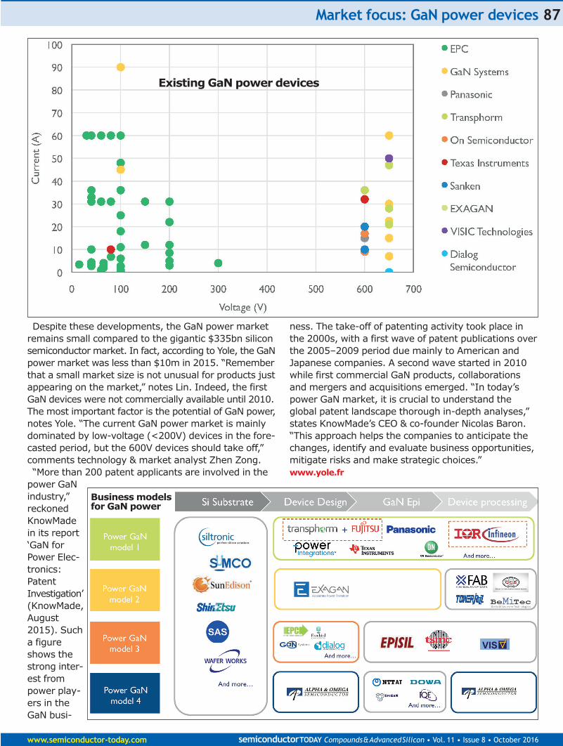
Despite these developments, the GaN power marketremains small compared to the gigantic $335bn siliconsemiconductor market. In fact, according to Yole, the GaNpower market was less than $10m in 2015. “Rememberthat a small market size is not unusual for products justappearing on the market,” notes Lin. Indeed, the firstGaN devices were not commercially available until 2010.The most important factor is the potential of GaN power,notes Yole. “The current GaN power market is mainlydominated by low-voltage (<200V) devices in the fore-casted period, but the 600V devices should take off,”comments technology & market analyst Zhen Zong. “More than 200 patent applicants are involved in the
power GaNindustry,”reckonedKnowMadein its report‘GaN forPower Elec-tronics:PatentInvestigation’(KnowMade,August2015). Sucha figureshows thestrong inter-est frompower play-ers in theGaN busi-
ness. The take-off of patenting activity took place inthe 2000s, with a first wave of patent publications overthe 2005–2009 period due mainly to American andJapanese companies. A second wave started in 2010while first commercial GaN products, collaborationsand mergers and acquisitions emerged. “In today’spower GaN market, it is crucial to understand theglobal patent landscape thorough in-depth analyses,”states KnowMade’s CEO & co-founder Nicolas Baron.“This approach helps the companies to anticipate thechanges, identify and evaluate business opportunities,mitigate risks and make strategic choices.” www.yole.fr
Market focus: GaN power devices
www.semiconductor-today.com semiconductorTODAY Compounds&AdvancedSilicon • Vol. 11 • Issue 8 • October 2016
87
Existing GaN power devices
Business modelsfor GaN power

Korea Institute of Science and Technology (KIST)claims a record low subthreshold swing of68mV/decade for a gallium arsenide (GaAs)
field-effect transistor (FET) [SangHyeon Kim et al,IEEE Electron Device Letters, published online 24 August 2016]. In addition, the double-gate (DG)
Technology focus: GaAs transistors 88
Figure 1. (a) Fabrication process flow of GaAs-OI FETs on Si via wafer bonding and ELO. Thicknesses of eachlayer are also shown (nm). (b) Schematic images of final device structures of SG and DG GaAs-OI FETs. (c) Cross-section transmission electron micrograph of fabricated GaAs-OI FETs on Si substrates.
semiconductorTODAY Compounds&AdvancedSilicon • Vol. 11 • Issue 8 • October 2016 www.semiconductor-today.com
Reducing subthreshold swingof gallium arsenide transistorsResearchers based in Korea claim a record low value of 68mV/decade.
(a) (b)
(c)
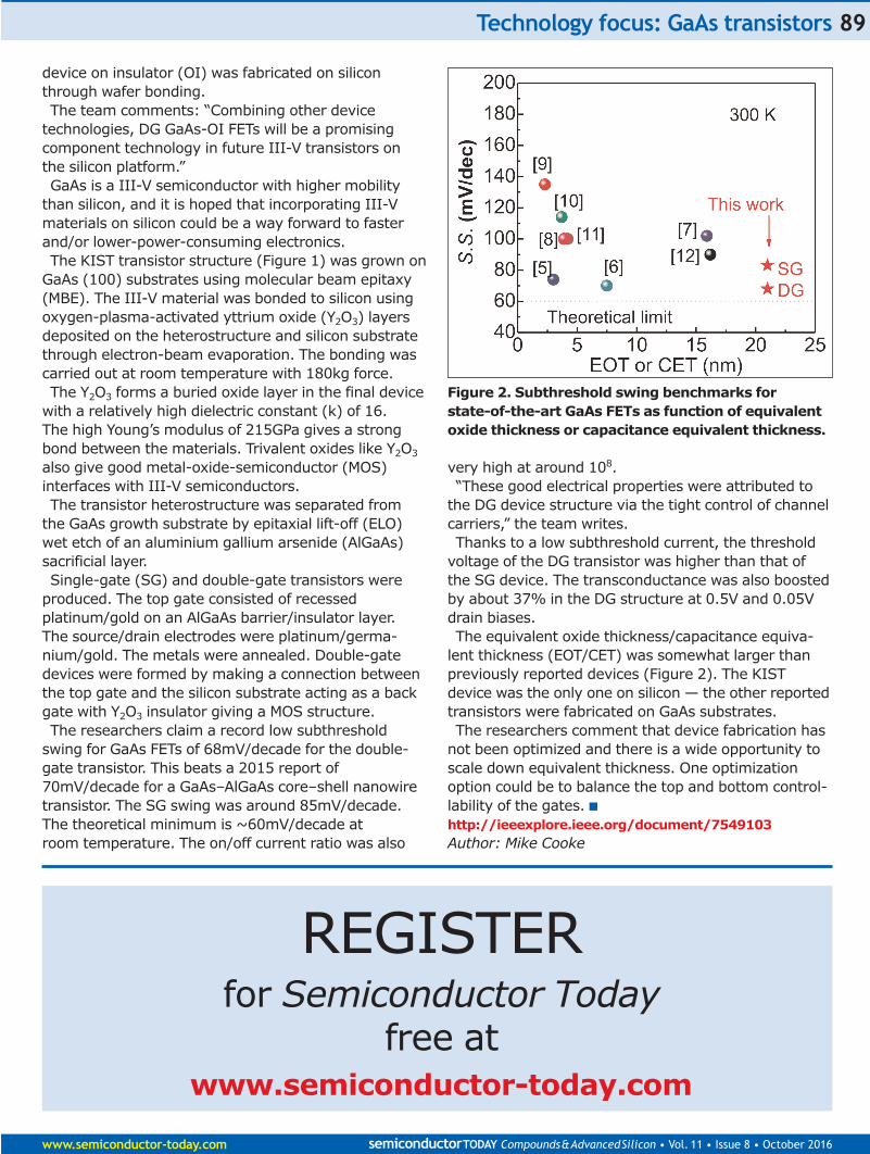
Technology focus: GaAs transistors
www.semiconductor-today.com semiconductorTODAY Compounds&AdvancedSilicon • Vol. 11 • Issue 8 • October 2016
89
device on insulator (OI) was fabricated on siliconthrough wafer bonding.The team comments: “Combining other device
technologies, DG GaAs-OI FETs will be a promisingcomponent technology in future III-V transistors onthe silicon platform.” GaAs is a III-V semiconductor with higher mobility
than silicon, and it is hoped that incorporating III-Vmaterials on silicon could be a way forward to fasterand/or lower-power-consuming electronics.The KIST transistor structure (Figure 1) was grown on
GaAs (100) substrates using molecular beam epitaxy(MBE). The III-V material was bonded to silicon usingoxygen-plasma-activated yttrium oxide (Y2O3) layersdeposited on the heterostructure and silicon substratethrough electron-beam evaporation. The bonding wascarried out at room temperature with 180kg force.The Y2O3 forms a buried oxide layer in the final device
with a relatively high dielectric constant (k) of 16. The high Young’s modulus of 215GPa gives a strongbond between the materials. Trivalent oxides like Y2O3
also give good metal-oxide-semiconductor (MOS)interfaces with III-V semiconductors. The transistor heterostructure was separated from
the GaAs growth substrate by epitaxial lift-off (ELO)wet etch of an aluminium gallium arsenide (AlGaAs)sacrificial layer.Single-gate (SG) and double-gate transistors were
produced. The top gate consisted of recessed platinum/gold on an AlGaAs barrier/insulator layer. The source/drain electrodes were platinum/germa-nium/gold. The metals were annealed. Double-gatedevices were formed by making a connection betweenthe top gate and the silicon substrate acting as a backgate with Y2O3 insulator giving a MOS structure.The researchers claim a record low subthreshold
swing for GaAs FETs of 68mV/decade for the double-gate transistor. This beats a 2015 report of70mV/decade for a GaAs–AlGaAs core–shell nanowiretransistor. The SG swing was around 85mV/decade.The theoretical minimum is ~60mV/decade at room temperature. The on/off current ratio was also
very high at around 108.“These good electrical properties were attributed to
the DG device structure via the tight control of channelcarriers,” the team writes.Thanks to a low subthreshold current, the threshold
voltage of the DG transistor was higher than that ofthe SG device. The transconductance was also boostedby about 37% in the DG structure at 0.5V and 0.05Vdrain biases.The equivalent oxide thickness/capacitance equiva-
lent thickness (EOT/CET) was somewhat larger thanpreviously reported devices (Figure 2). The KISTdevice was the only one on silicon — the other reportedtransistors were fabricated on GaAs substrates. The researchers comment that device fabrication has
not been optimized and there is a wide opportunity toscale down equivalent thickness. One optimizationoption could be to balance the top and bottom control-lability of the gates. ■http://ieeexplore.ieee.org/document/7549103Author: Mike Cooke
Figure 2. Subthreshold swing benchmarks for state-of-the-art GaAs FETs as function of equivalentoxide thickness or capacitance equivalent thickness.
REGISTERfor Semiconductor Today
free at www.semiconductor-today.com

Aresearch team led by faculty scientist Ali Javeyat the US Department of Energy’s LawrenceBerkeley National Laboratory (Berkeley Lab)
has created a working transistor with a gate length(the defining dimension of a transistor) just 1nm long,which is the smallest reported to date (‘MoS2 transistorswith 1-nanometer gate lengths’, Science Vol. 354,Issue 6308, p99–102). For conventional semiconductors, the laws of physics
set a 5nm threshold on the size of transistor gates(about a quarter the size of high-end 20nm-gate transistors currently on the market). However, the1nm-gate transistor show that “with the choice ofproper materials, there is a lot more room to shrinkour electronics,” says Javey, lead principal investigatorof the Electronic Materials program in Berkeley Lab’sMaterials Science Division (and a University of California Berkeley professor of electrical engineering
and computer sciences). The key was to use carbonnanotubes and molybdenum disulfide (MoS2). Other investigators on the paper include Jeff Bokor,
a senior faculty scientist at Berkeley Lab and a professor at UC Berkeley; Chenming Hu, a professor at UC Berkeley; Moon Kim, a professor at the University of Texas at Dallas; and H.S. Philip Wong, a professor at Stanford University. The new development could be key to keeping alive
Intel co-founder Gordon Moore’s prediction that thedensity of transistors on integrated circuits would doubleevery two years. “The semiconductor industry has long assumed that
any gate below 5nm wouldn’t work, so anything belowthat was not even considered,” says study lead authorSujay Desai, a graduate student in Javey’s lab. “This research shows that sub-5nm gates should not bediscounted. Industry has been squeezing every last bit
Technology focus: 2D transistors 90
Schematic of transistor with a MoS2 channel and 1nm carbon nanotube gate. (Courtesy of Sujay Desai/Berkeley Lab.)
semiconductorTODAY Compounds&AdvancedSilicon • Vol. 11 • Issue 7 • September 2016 www.semiconductor-today.com
Berkeley Lab-led teamfabricates transistor withrecord 1nm-long gate Proof of concept using MoS2 channel with carbon nanotube gate points way tosub-5nm transistors

Technology focus: 2D transistors
www.semiconductor-today.com semiconductorTODAY Compounds&AdvancedSilicon • Vol. 11 • Issue 8 • October 2016
91
of capability out of silicon. By changing the material fromsilicon to MoS2, we can make a transistor with a gatethat is just 1nm in length, and operate it like a switch.” Both silicon and MoS2 have a crystalline lattice struc-
ture, but electrons flowing through silicon are lighterand encounter less resistance compared with MoS2.That is a benefit when the gate is 5nm or more, butbelow that length the quantum mechanical phenomenonof tunneling kicks in and the gate barrier is no longerable to keep the electrons from barging through fromthe source to the drain terminals. “This means we can’tturn off the transistors,” says Desai. “The electrons areout of control.” Because electrons flowing through MoS2 are heavier,
their flow can be controlled with smaller gate lengths.MoS2 can also be scaled down to atomically thin sheets(about 0.65nm thick) with a lower dielectric constant(reflecting the ability of the material to store energy inan electric field). Both of these properties, in additionto the mass of the electron, help to improve the controlof current flow inside the transistor when the gatelength is reduced to 1nm.
For constructing the transistor’s gate, conventionallithography techniques do not work well at a scale of1nm, so the researchers turned to hollow cylindricalcarbon nanotubes with diameters as small as 1nm.They then measured the electrical properties of thedevices to show that the MoS2 transistor with the carbon nanotube gate effectively controlled the flow ofelectrons. “However, it’s a proof of concept. We have not yet
packed these transistors onto a chip, and we haven’tdone this billions of times over,” notes Javey. “We alsohave not developed self-aligned fabrication schemesfor reducing parasitic resistances in the device. But this work is important to show that we are no longerlimited to a 5nm gate for our transistors. Moore’s Lawcan continue a while longer by proper engineering ofthe semiconductor material and device architecture.” The work at Berkeley Lab was funded primarily by
the Department of Energy’s Basic Energy Sciences program. ■http://science.sciencemag.org/content/354/6308/99 http://emat.lbl.gov
Transmission electron microscope image of transistor cross-section, showing 1nm carbon nanotube gate and MoS2
semiconductor separated by the insulator zirconium dioxide. (Courtesy of Qingxiao Wang, UT Dallas.)

semiconductorTODAY Compounds&AdvancedSilicon • Vol. 11 • Issue 8 • October 2016 www.semiconductor-today.com
92
suppliers’ directory
1 Bulk crystal source materials p92
2 Bulk crystal growth equipment p92
3 Substrates p92
4 Epiwafer foundry p93
5 Deposition materials p93
6 Deposition equipment p94
7 Wafer processing materials p94
8 Wafer processing equipment p95
9 Materials and metals p95
10 Gas & liquid handling equipment p95
11 Process monitoring and control p95
12 Inspection equipment p96
13 Characterization equipment p96
14 Chip test equipment p96
15 Assembly/packaging materials p96
16 Assembly/packaging equipment p96
17 Assembly/packaging foundry p96
18 Chip foundry p96
19 Facility equipment p96
20 Facility consumables p96
21 Computer hardware & software p96
22 Used equipment p97
23 Services p97
24 Consulting p97
25 Resources p97
1 Bulk crystal sourcematerials
Mining & Chemical Products Ltd(part of 5N Plus, Inc) 1-4, Nielson Road, Finedon Road Industrial Estate, Wellingborough, Northants NN8 4PE, UK Tel: +44 1933 220626 Fax: +44 1933 227814 www.MCP-group.com
Umicore Indium Products 50 Simms Avenue, Providence, RI 02902, USA Tel: +1 401 456 0800 Fax: +1 401 421 2419 www.thinfilmproducts.umicore.com
United Mineral & Chemical Corp 1100 Valley Brook Avenue, Lyndhurst, NJ 07071, USA Tel: +1 201 507 3300 Fax: +1 201 507 1506 www.umccorp.com
2 Bulk crystal growthequipment
MR Semicon Inc PO Box 91687, Albuquerque, NM 87199-1687, USA Tel: +1 505 899 8183 Fax: +1 505 899 8172 www.mrsemicon.com
3 Substrates
AXT Inc 4281 Technology Drive, Fremont, CA 94538, USA Tel: +1 510 438 4700Fax: +1 510 683 5901 www.axt.com Supplies GaAs, InP, and Ge wafersusing VGF technology withmanufacturing facilities in Beijingand five joint ventures in Chinaproducing raw materials, includingGa, As, Ge, pBN, B2O3.
CrystAl-N GmbHDr.-Mack-Straße 77, D-90762Fürth, GermanyTel: +49 (0)911 650 78 650 90Fax: +49 (0)911 650 78 650 93E-mail: [email protected] www.crystal-n.com
Crystal IS Inc70 Cohoes AvenueGreen Island, NY 12183, USATel: +1 518 271 7375Fax: +1 518 271 7394www.crystal-is.com
Freiberger Compound Materials Am Junger Loewe Schacht 5, Freiberg, 09599, Germany Tel: +49 3731 280 0 Fax: +49 3731 280 106 www.fcm-germany.com
Kyma Technologies Inc 8829 Midway West Road, Raleigh, NC, USA Tel: +1 919 789 8880 Fax: +1 919 789 8881 www.kymatech.com
Index
To have your company listed in this directory, e-mail details (including categories) to [email protected]: advertisers receive a free listing. For all other companies, a charge is applicable.

Suppliers’ Directory
www.semiconductor-today.com semiconductorTODAY Compounds&AdvancedSilicon • Vol. 11 • Issue 8 • October 2016
93
MARUWA CO LTD 3-83, Minamihonjigahara-cho,Owariasahi, Aichi 488-0044, JapanTel: +81 572 52 2317www.maruwa-g.com/e/products/ceramic
MARUWA is a global supplier ofceramic substrates and wafers madeof aluminium nitride (AlN), alumina(Al2O3), ZTA and silicon nitride(Si3N4). Products meet requiredproperties such as high thermalconductivity and bending strengthfor power devices, especiallywafers are suitable as a bondingwafer (GaN, SOI) for epi wafers.
sp3 Diamond Technologies2220 Martin Avenue, Santa Clara, CA 95050, USA Tel: +1 877 773 9940Fax: +1 408 492 0633www.sp3inc.com
Sumitomo ElectricSemiconductor Materials Inc 7230 NW Evergreen Parkway, Hillsboro, OR 97124, USA Tel: +1 503 693 3100 x207 Fax: +1 503 693 8275 www.sesmi.com
III/V-ReclaimWald 10, 84568 Pleiskirchen, Germany Tel: +49 8728 911 093Fax: +49 8728 911 156www.35reclaim.deIII/V-Reclaim offers reclaim(recycling) of GaAs and InP wafers,removing all kinds of layers andstructures from customers’ wafers.All formats and sizes can behandled. The firm offers single-sideand double-side-polishing andready-to-use surface treatment.
Umicore Electro-Optic MaterialsWatertorenstraat 33, B-2250 Olen, BelgiumTel: +32-14 24 53 67Fax: +32-14 24 58 00www.substrates.umicore.com
Wafer World Inc1100 Technology Place, Suite 104,West Palm Beach, FL 33407, USATel: +1-561-842-4441Fax: +1-561-842-2677E-mail: [email protected]
4 Epiwafer foundry
Spire Semiconductor LLC 25 Sagamore Park Drive, Hudson, NH 03051, USA Tel: +1 603 595 8900 Fax: +1 603 595 0975 www.spirecorp.com
Albemarle Cambridge Chemical LtdUnit 5 Chesterton Mills, French’s Road, Cambridge CB4 3NP, UKTel: +44 (0)1223 352244Fax: +44 (0)1223 352444www.camchem.co.uk
Intelligent Epitaxy Technology Inc 1250 E Collins Blvd, Richardson, TX 75081-2401, USATel: +1 972 234 0068Fax: +1 972 234 0069www.intelliepi.com
IQE Cypress Drive, St Mellons, CardiffCF3 0EG, UK Tel: +44 29 2083 9400 Fax: +44 29 2083 9401 www.iqep.com IQE is a leading global supplier ofadvanced epiwafers, with productscovering a diverse range ofapplications within the wireless,optoelectronic, photovoltaic andelectronic markets.
OMMIC 2, Chemin du Moulin B.P. 11, Limeil-Brevannes, 94453, France Tel: +33 1 45 10 67 31 Fax: +33 1 45 10 69 53 www.ommic.fr
SoitecPlace Marcel Rebuffat, Parc deVillejust, 91971 Courtabouef, France Tel: +33 (0)1 69 31 61 30 Fax: +33 (0)1 69 31 61 79www.picogiga.com
5 Depositionmaterials
Akzo Nobel High Purity Metalorganics www.akzonobel.com/hpmo Asia Pacific: Akzo Nobel (Asia) Co Ltd,Shanghai, ChinaTel. +86 21 2216 3600Fax: +86 21 3360 [email protected] Americas: AkzoNobel Functional Chemicals,Chicago, USA Tel. +31 800 828 7929 (US only)Tel: +1 312 544 7000Fax: +1 312 544 [email protected] Europe, Middle East and Africa: AkzoNobel Functional Chemicals,Amersfoort, The NetherlandsTel. +31 33 467 6656Fax: +31 33 467 [email protected]
Cambridge Chemical Company LtdUnit 5 Chesterton Mills, French’s Road, Cambridge CB4 3NP, UKTel: +44 (0)1223 352244Fax: +44 (0)1223 352444www.camchem.co.uk
Dow Electronic Materials 60 Willow Street, North Andover, MA 01845, USA Tel: +1 978 557 1700 Fax: +1 978 557 1701 www.metalorganics.com
Matheson Tri-Gas6775 Central Avenue, Newark, CA 94560, USA

Tel: +1 510 793 2559Fax: +1 510 790 6241www.mathesontrigas.com
Mining & Chemical Products Ltd (see section 1 for full contact details)
Praxair Electronics 542 Route 303, Orangeburg, NY 10962, USA Tel: +1 845 398 8242 Fax: +1 845 398 8304 www.praxair.com/electronics
SAFC HitechPower Road, Bromborough, Wirral, Merseyside CH62 3QF, UKTel: +44 151 334 2774Fax: +44 151 334 6422www.safchitech.com
Materion Advanced MaterialsGroup2978 Main Street, Buffalo, NY 14214, USATel: +1 716 837 1000Fax: +1 716 833 2926www.williams-adv.com
6 Depositionequipment
AIXTRON SEDornkaulstr. 2, 52134 Herzogenrath, Germany Tel: +49 2407 9030 0 Fax: +49 2407 9030 40 www.aixtron.com
AIXTRON is a leading provider ofdeposition equipment to thesemiconductor industry. Thecompany’s technology solutions areused by a diverse range of customersworldwide to build advancedcomponents for electronic andoptoelectronic applications(photonic) based on compound,silicon, or organic semiconductormaterials and, more recently,carbon nanotubes (CNT), grapheneand other nanomaterials.
Evatec AG Hauptstrasse 1a, CH-9477 Trübbach, Switzerland Tel: +41 81 403 8000Fax: +41 81 403 8001www.evatecnet.com
Ferrotec-Temescal 4569-C Las Positas Rd, Livermore, CA 94551, USA Tel: +1 925 245 5817 Fax: +1 925 449-4096www.temescal.net Temescal, the expert inmetallization systems for theprocessing of compoundsemiconductor-based substrates,provides the finest evaporationsystems available. Multi-layercoatings of materials such as Ti, Pt, Au, Pd, Ag, NiCr, Al, Cr, Cu,Mo, Nb, SiO2, with high uniformityare guaranteed. Today the world’smost sophisticated handsets,optical, wireless and telecomsystems rely on millions of devices that are made usingTemescal deposition systems andcomponents.
Oxford Instruments Plasma Technology North End, Yatton, Bristol, Avon BS49 4AP, UK Tel: +44 1934 837 000 Fax: +44 1934 837 001 www.oxford-instruments.co.uk We provide flexible tools and processes for precise materials deposition,etching and controlled nanostructuregrowth. Core technologies includeplasma and ion-beam depositionand etch and ALD.
Plasma-Therm LLC10050 16th Street North, St. Petersburg, FL 33716, USA Tel: +1 727 577 4999 Fax: +1 727 577 7035 www.plasmatherm.com www.plasmatherm.com
Plasma-Therm, LLC is an establishedleading provider of advancedplasma processing equipment forthe semiconductor industry andrelated specialty markets.
Riber 31 rue Casimir Périer, BP 70083,95873 Bezons Cedex, France Tel: +33 (0) 1 39 96 65 00Fax: +33 (0) 1 39 47 45 62www.riber.com
SVT Associates Inc7620 Executive Drive, Eden Prairie, MN 55344, USATel: +1 952 934 2100Fax: +1 952 934 2737www.svta.com
Veeco Instruments Inc 100 Sunnyside Blvd., Woodbury, NY 11797, USA Tel: +1 516 677 0200 Fax: +1 516 714 1231 www.veeco.com
Veeco is a world-leading supplier ofcompound semiconductor equipment,and the only company offering bothMOCVD and MBE solutions. Withcomplementary AFM technology andthe industry’s most advanced ProcessIntegration Center, Veeco tools helpgrow and measure nanoscale devicesin worldwide LED/wireless, datastorage, semiconductor and scientificresearch markets—offering importantchoices, delivering ideal solutions.
7 Wafer processingmaterials
Air Products and Chemicals Inc 7201 Hamilton Blvd., Allentown, PA 18195, USA Tel: +1 610 481 4911 www.airproducts.com/compound
MicroChem Corp1254 Chestnut St. Newton, MA 02464, USA Tel: +1 617 965 5511Fax: +1 617 965 5818www.microchem.com
Suppliers’ Directory
semiconductorTODAY Compounds&AdvancedSilicon • Vol. 11 • Issue 8 • October 2016 www.semiconductor-today.com
94

Praxair Electronics (see section 5 for full contact details)
8 Wafer processingequipment
EV GroupDI Erich Thallner Strasse 1, St. Florian/Inn, 4782, Austria Tel: +43 7712 5311 0 Fax: +43 7712 5311 4600 www.EVGroup.comTechnology and market leader for wafer processing equipment. Worldwide industry standards foraligned wafer bonding, resistprocessing for the MEMS, nano andsemiconductor industry.
Logitech LtdErskine Ferry Road, Old Kilpatrick, near Glasgow G60 5EU, Scotland, UKTel: +44 (0) 1389 875 444Fax: +44 (0) 1389 879 042www.logitech.uk.com
Oxford Instruments Plasma Technology (see section 6 for full contact details)
Plasma-Therm LLC(see section 6 for full contact details)
SAMCO International Inc 532 Weddell Drive, Sunnyvale, CA, USA Tel: +1 408 734 0459 Fax: +1 408 734 0961 www.samcointl.com
SPTS Technology Ltd Ringland Way, Newport NP18 2TA, UK Tel: +44 (0)1633 414000 Fax: +44 (0)1633 414141 www.spts.com
SUSS MicroTec AGSchleißheimer Strasse 90, 85748 Garching,
Germany Tel: +49 89 32007 0 Fax: +49 89 32007 162 www.suss.com
Veeco Instruments Inc (see section 6 for full contact details)
9 Materials & metals
Goodfellow Cambridge LtdErmine Business Park, Huntingdon, Cambridgeshire PE29 6WR, UKTel: +44 (0) 1480 424800Fax: +44 (0) 1480 424900www.goodfellow.com
Goodfellow supplies smallquantities of metals and materialsfor research, development,prototyping and specialisedmanufacturing operations.
10 Gas and liquidhandling equipment
Air Products and Chemicals Inc (see section 7 for full contact details)
Cambridge Fluid Systems12 Trafalgar Way, Bar Hill, Cambridge CB3 8SQ, UK Tel: +44 (0)1954 786800 Fax: +44 (0)1954 786818 www.cambridge-fluid.com
CS CLEAN SYSTEMS AGFraunhoferstrasse 4, Ismaning, 85737, Germany Tel: +49 89 96 24 00 0 Fax: +49 89 96 24 00 122 www.cscleansystems.com
SAES Pure Gas Inc 4175 Santa Fe Road, San Luis Obispo, CA 93401, USA Tel: +1 805 541 9299 Fax: +1 805 541 9399 www.saesgetters.com
11 Process monitoringand control
k-Space Associates 2182 Bishop Circle East, Dexter, MI 48130, USA Tel: +1 734 426 7977 Fax: +1 734 426 7955www.k-space.com k-Space Associates Inc specializes inin-situ, real-time thin-film processmonitoring tools for MBE, MOCVD,PVD, and thermal evaporation.Applications and materials includethe research and production linemonitoring of compoundsemiconductor-based electronic,optoelectronic, and photovoltaicdevices.
KLA-Tencor One Technology Dr, 1-2221I, Milpitas, CA 95035, USA Tel: +1 408 875 3000 Fax: +1 408 875 4144www.kla-tencor.com
LayTec AG Seesener Str. 10–13,10709 Berlin,Germany Tel: +49 30 89 00 55 0 Fax: +49 30 89 00 180 www.laytec.de LayTec develops and manufacturesoptical in-situ and in-line metrologysystems for thin-film processeswith particular focus on compoundsemiconductor and photovoltaicapplications. Its know-how is based on optical techniques:reflectometry, emissivity correctedpyrometry, curvaturemeasurements and reflectanceanisotropy spectroscopy.
WEP (Ingenieurbüro Wolff für Elektronik- undProgrammentwicklungen) Bregstrasse 90, D-78120Furtwangen im Schwarzwald, GermanyTel: +49 7723 9197 0 Fax: +49 7723 9197 22 www.wepcontrol.com
Suppliers’ Directory
www.semiconductor-today.com semiconductorTODAY Compounds&AdvancedSilicon • Vol. 11 • Issue 8 • October 2016
95
Inc

Suppliers’ Directory
semiconductorTODAY Compounds&AdvancedSilicon • Vol. 11 • Issue 8 • October 2016 www.semiconductor-today.com
96
12 Inspection equipment
Bruker AXS GmbH Oestliche Rheinbrueckenstrasse 49, Karlsruhe, 76187, Germany Tel: +49 (0)721 595 2888 Fax: +49 (0)721 595 4587 www.bruker-axs.de
13 Characterizationequipment
J.A. Woollam Co. Inc. 645 M Street Suite 102, Lincoln, NE 68508, USA Tel: +1 402 477 7501 Fax: +1 402 477 8214 www.jawoollam.com
Lake Shore Cryotronics Inc 575 McCorkle Boulevard, Westerville, OH 43082, USA Tel: +1 614 891 2244 Fax: +1 614 818 1600 www.lakeshore.com
14 Chip test equipment
Keithley Instruments Inc28775 Aurora Road, Cleveland, OH 44139, USA Tel: +1 440.248.0400 Fax: +1 440.248.6168 www.keithley.com
15 Assembly/packagingmaterials
ePAK International Inc 4926 Spicewood Springs Road, Austin, TX 78759, USA Tel: +1 512 231 8083 Fax: +1 512 231 8183 www.epak.com
Gel-Pak 31398 Huntwood Avenue, Hayward, CA 94544, USA Tel: +1 510 576 2220Fax: +1 510 576 2282www.gelpak.com
Wafer World Inc (see section 3 for full contact details)
Materion Advanced MaterialsGroup2978 Main Street, Buffalo, NY 14214, USATel: +1 716 837 1000Fax: +1 716 833 2926www.williams-adv.com
16 Assembly/packagingequipment
Ismeca Europe Semiconductor SAHelvetie 283, La Chaux-de-Fonds,2301, Switzerland Tel: +41 329257111 Fax: +41 329257115 www.ismeca.com
Kulicke & Soffa Industries1005 Virginia Drive, Fort Washington, PA 19034, USA Tel: +1 215 784 6000Fax: +1 215 784 6001 www.kns.com
Palomar Technologies Inc 2728 Loker Avenue West, Carlsbad, CA 92010, USA Tel: +1 760 931 3600 Fax: +1 760 931 5191 www.PalomarTechnologies.com
TECDIA Inc 2700 Augustine Drive, Suite 110,Santa Clara, CA 95054, USATel: +1 408 748 0100Fax: +1 408 748 0111www.tecdia.com
17 Assembly/packagingfoundry
Quik-Pak10987 Via Frontera, San Diego, CA 92127, USA Tel: +1 858 674 4676 Fax: +1 8586 74 4681 www.quikicpak.com
18 Chip foundry
Compound SemiconductorTechnologies Ltd Block 7, Kelvin Campus, West of Scotland, Glasgow, Scotland G20 0TH, UK Tel: +44 141 579 3000 Fax: +44 141 579 3040 www.compoundsemi.co.uk
United Monolithic Semiconductors Route departementale 128, BP46, Orsay, 91401, France Tel: +33 1 69 33 04 72 Fax: +33 169 33 02 92 www.ums-gaas.com
19 Facility equipment
MEI, LLC3474 18th Avenue SE, Albany, OR 97322-7014, USA Tel: +1 541 917 3626Fax: +1 541 917 3623www.marlerenterprises.net
20 Facility consumables
W.L. Gore & Associates401 Airport Rd, Elkton, MD 21921-4236, USA Tel: +1 410 392 4440Fax: +1 410 506 8749www.gore.com
21 Computer hardware& software
Ansoft Corp4 Station Square, Suite 200, Pittsburgh, PA 15219, USATel: +1 412 261 3200 Fax: +1 412 471 9427 www.ansoft.com
Crosslight Software Inc121-3989 Henning Dr., Burnaby, BC, V5C 6P8, Canada Tel: +1 604 320 1704Fax: +1 604 320 1734www.crosslight.com

Semiconductor TechnologyResearch Inc10404 Patterson Ave., Suite 108,Richmond, VA 23238, USATel: +1 804 740 8314Fax: +1 804 740 3814www.semitech.us
22 Used equipment
Class One Equipment Inc 5302 Snapfinger Woods Drive, Decatur, GA 30035, USATel: +1 770 808 8708Fax: +1 770 808 8308www.ClassOneEquipment.com
23 Services
Henry Butcher InternationalBrownlow House, 50–51
High Holborn, London WC1V 6EG, UK Tel: +44 (0)20 7405 8411 Fax: +44 (0)20 7405 9772 www.henrybutcher.com
M+W Zander Holding AGLotterbergstrasse 30, Stuttgart, Germany Tel: +49 711 8804 1141 Fax: +49 711 8804 1950 www.mw-zander.com
24 Consulting
Fishbone Consulting SARL8 Rue de la Grange aux Moines, 78460 Choisel, France Tel: + 33 (0)1 30 47 29 03E-mail: [email protected]
25 Resources
Al Shultz Advertising Marketing for AdvancedTechnology Companies 1346 The Alameda, 7140 San Jose, CA 95126, USA Tel: +1 408 289 9555 www.alshuktz.com
SEMI Global Headquarters3081 Zanker Road, San Jose, CA 95134, USATel: +1 408 943 6900Fax: +1 408 428 9600www.semi.org
Yole Développement 45 rue Sainte Geneviève, 69006 Lyon, France Tel: +33 472 83 01 86www.yole.fr
REGISTERfor Semiconductor Today
free at
www.semiconductor-today.com
Suppliers’ Directory
www.semiconductor-today.com semiconductorTODAY Compounds&AdvancedSilicon • Vol. 11 • Issue 8 • October 2016
97

7 November 2016 Imec Technology Forum ITF2016 Japan New Otani Hotel – Tokyo, Japan E-mail: [email protected] www.itf2016.be/page.aspx/2218
7–9 November 2016 4th IEEE Workshop on Wide Bandgap PowerDevices and Applications (WiPDA 2016) Fayetteville, AR USA E-mail: [email protected] www.wipda2016.org
13–16 November 2016 11th International Conference on AdvancedSemiconductor Devices & Microsystems(ASDAM ’16) Smolenice, Slovakia E-mail: [email protected] http://elu.sav.sk/asdam
3–7 December 2016IEDM 2016: 62nd annual IEEE International ElectronDevices Meeting San Francisco Union Square Hilton Hotel, CA, USA E-mail: [email protected] www.ieee-iedm.org
7–10 December 2016 47th IEEE Semiconductor InterfaceSpecialists Conference (SISC 2016) Catamaran Hotel, San Diego, CA, USAwww.ieeesisc.org
13–14 December 2016 International MicroNanoConference 2016 Beurs van Berlage, Amsterdam, The Netherlands E-mail: [email protected] www.micronanoconference.org
14–16 December 2016 SEMICON Japan 2016 Tokyo International Exhibition Center (Tokyo Big Sight),Japan E-mail: [email protected] www.semiconjapan.org
27–30 December 2016 3rd International Conference on EmergingElectronics (ICEE 2016) Indian Institute of Technology Bombay (IIT Bombay),Mumbai, India E-mail: [email protected] www.iceeconf.org
28 January – 2 February 2017SPIE Photonics West 2017Moscone Center, San Francisco, CA, USA E-mail: [email protected] http://spie.org/SPIE-PHOTONICS-WEST-conference
5–9 February 2017 IEEE International Solid-State CircuitsConference (ISSCC 2017) San Francisco, CA, USA E-mail: [email protected] www.isscc.org
semiconductorTODAY Compounds&AdvancedSilicon • Vol. 11 • Issue 8 • October 2016 www.semiconductor-today.com
98
event calendarIf you would like your event listed in Semiconductor Today’s Event Calendar,then please e-mail all details to the Editor at [email protected]
Aixtron SE 5Evatec 45Ferrotec-Temescal 49Fuji Electric 23IQE 25Logitech 33RIFF Company 59
SEMI-GAS 35Umicore 43University Wafer 52Veeco Instruments — MBE 9Veeco Instruments — MOCVD 2Wafer World 29
Advertiser Page no. Advertiser Page no.
advertisers’ index

28 February – 2 March 2017 IEEE Electron Devices Technology andManufacturing Conference (EDTM 2017) Toyama International Conference Center, Japan E-mail: [email protected] http://ewh.ieee.org/conf/edtm/2017
14–16 March 2017 SEMICON China 2017 Shanghai New International Expo Centre, China E-mail: [email protected] www.semiconchina.org
19–23 March 2017 Optical Fiber Communication Conference &Exhibition (OFC 2017) Los Angeles Convention Center, CA, USA E-mail: [email protected] www.ofcconference.org
3–5 April 2017 19th European Conference on IntegratedOptics (ECIO 2017) Technical University of Eindhoven, The Netherlands E-mail: [email protected] www.ecio-conference.org
3–5 April 20172017 Joint International EUROSOIWorkshop and International Conference onUltimate Integration on Silicon (ULIS) Institute of Nanoscience & Nanotechnology of NCSR‘Demokritos’, Athens, Greece E-mail: [email protected] www.eurosoi-ulis2017.inn.demokritos.gr
9–13 April 2017SPIE Defense + Commercial Sensing (DCS 2017)Anaheim Convention Center, CA, USA E-mail: [email protected]://spie.org/SPIE-DCS-conference
18–21 April 2017 SNEC's 11th International PhotovoltaicPower Generation Conference & Exhibition(SNEC PV Power EXPO 2017) Shanghai, ChinaE-mail: [email protected] www.snec.org.cn
1–3 May 2017 13th International Conference onConcentrator Photovoltaics (CPV-13) University of Ottawa, Canada E-mail: [email protected] www.cpv-13.org
22–25 May 2017 2017 CS ManTech (International Conferenceon Compound Semiconductor ManufacturingTechnology) Hyatt Regency Indian Wells Resort & Spa, Indian Wells,CA, USA E-mail: [email protected] www.csmantech.org
28 May – 1 June 2017 29th International Symposium on PowerSemiconductor Devices and ICs (ISPSD 2017) Sapporo, Japan E-mail: [email protected]://eds.ieee.org/eds-meetings-calendars.html
4–6 June 2017 IEEE Radio Frequency Integrated CircuitsSymposium (RFIC 2017) Hawaii Convention Center, Honolulu, HI, USAhttp://rfic-ieee.org
25–30 June 2017 44th IEEE Photovoltaic SpecialistsConference (PVSC 2017) Marriot Wardman Park Hotel, Washington DC, USA E-mail: [email protected] www.ieee-pvsc.org/PVSC44
10–12 July 2017 IEEE Photonics Society’s 2017 SummerTopicals Meeting Series San Juan, Puerto RicoE-mail: [email protected] www.sum-ieee.org
23–25 August 2017IEEE 14th International Conference onGroup IV Photonics (GFP 2017) Berlin, Germany E-mail: [email protected] www.gfp-ieee.org
22–25 October 2017 IEEE Compound Semiconductor IntegratedCircuit Symposium (CSICS 2017) Miami, FL USA E-mail: [email protected] https://csics.org
26–28 October 2017 International Conference on AdvancedMaterials and NanotechnologyOsaka, Japan http://advancedmaterials.conferenceseries.com/events-list/photonics-and-semiconductor-nanophysics
Event Calendar
www.semiconductor-today.com semiconductorTODAY Compounds&AdvancedSilicon • Vol. 11 • Issue 8 • October 2016
99

Choose Semiconductor Today for . . .
MAGAZINE
Accurate and timely coverage of the compound semiconductor and advanced silicon industries
Published 10 times a year and delivered by e-mail and RSS feeds
Targeted 41,000+ international circulation
WEB SITE
Average of over 19,700 unique visitors to the site each month
Google-listed news source
Daily news updates and regular feature articles
E-BRIEF
Weekly round-up of key business and technical news
E-mail delivery to entire circulation
Banner and text marketing opportunities available
www.semiconductor-today.com
Follow us on Twitter: Semiconductor_T
Join our LinkedIn group: Semiconductor Today
semiconductorTODAYC O M P O U N D S & A D V A N C E D S I L I C O NVol.7 • Issue 2 • March/April 2012 www.semiconductor-today.com
Graphensic spun off •Emcore sells VCSEL range to Sumitomo Masimo buys Spire Semiconductor•Oclaro and Opnext merge
ISSN 1752-2935 (online)
Efficiency droop in nitride & phosphide LEDsFirst single-crystal gallium oxide FET
Efficiency droop in nitride & phosphide LEDsFirst single-crystal gallium oxide FET