Ultradense phosphorus in germanium delta-doped layers
9
Ultra-dense phosphorus in germanium delta-doped layers. G. Scappucci, 1 School of Physics and Australian Research Council Centre of Excellence for Quantum Computer Technology, University of New South Wales, Sydney, NSW 2052, Australia. G. Capellini, Dipartimento di Fisica, Università di Roma Tre, Via della Vasca Navale 84, 00146 Roma, Italy. W. C. T. Lee, and M. Y. Simmons School of Physics University of New South Wales, Sydney, NSW 2052, Australia. Abstract Phosphorus (P) in germanium (Ge) δ-doped layers are fabricated in ultra-high vacuum by adsorption of phosphine molecules onto an atomically flat clean Ge(001) surface followed by thermal incorporation of P into the lattice and epitaxial Ge overgrowth by molecular beam epitaxy. Structural and electrical characterizations show that P atoms are confined, with minimal diffusion, into an ultra-narrow 2-nm-wide layer with an electrically-active sheet carrier concentration of 4×10 13 cm -2 at 4.2 K. These results open up the possibility of ultra-narrow source/drain regions with unprecedented carrier densities for Ge n-channel field effect transistors. 1 Electronic mail: [email protected]; [email protected] 1
Transcript of Ultradense phosphorus in germanium delta-doped layers

Ultra-dense phosphorus in germanium delta-doped layers.
G. Scappucci,1
School of Physics and Australian Research Council Centre of Excellence for Quantum Computer
Technology, University of New South Wales, Sydney, NSW 2052, Australia.
G. Capellini,
Dipartimento di Fisica, Università di Roma Tre, Via della Vasca Navale 84, 00146 Roma, Italy.
W. C. T. Lee, and M. Y. Simmons
School of Physics University of New South Wales, Sydney, NSW 2052, Australia.
Abstract
Phosphorus (P) in germanium (Ge) δ-doped layers are fabricated in ultra-high vacuum by
adsorption of phosphine molecules onto an atomically flat clean Ge(001) surface followed by
thermal incorporation of P into the lattice and epitaxial Ge overgrowth by molecular beam epitaxy.
Structural and electrical characterizations show that P atoms are confined, with minimal diffusion,
into an ultra-narrow 2-nm-wide layer with an electrically-active sheet carrier concentration of
4×1013 cm-2 at 4.2 K. These results open up the possibility of ultra-narrow source/drain regions with
unprecedented carrier densities for Ge n-channel field effect transistors.
1 Electronic mail: [email protected]; [email protected]
1

On the roadmap of continuous device miniaturization beyond the 22 nm node, quasi-ballistic
operation with injection at the source-end is necessary to maintain high speed operation in
transistors.1 To accomplish this, technological progress other than silicon (Si) scaling is necessary,
including the use of alternative high mobility channel materials. Germanium (Ge) is a promising
candidate for the replacement of Si in the next generation of nanoscale metal oxide semiconductor
field effect transistors (MOSFETs) because the higher bulk mobility (∼ 3× higher for electrons and
∼ 5× for holes at room temperature) and the higher saturation velocity (∼ 7×) lead to maximum
drain current while minimizing leakage currents and power dissipation.2
Although the earliest transistor and integrated circuits were both fabricated in Ge, further progress
in Ge MOSFETs was hindered by the lack of a stable native oxide that could passivate the surface
and act as a high quality gate dielectric. Prompted by the renewed interest in Ge-based
nanoelectronics, the advancement on high permittivity (high-κ) dielectrics has now enabled the
fabrication of high-quality p-channel Ge MOSFETs.3 The development of satisfactory n-channel Ge
MOSFETs, however, is facing a major roadblock. Due to the enhanced diffusion of n-type dopants
in Ge compared with bulk Si, forming reliable n-type source-drain contacts within the thermal
budget allowed by high-κ dielectrics (T < 400 °C) has become a critical issue.4 Traditional ion
implantation has been so far inadequate to meet these requirements due to high temperatures
required for electrical activation of dopants. In this letter we present an ultra-high vacuum (UHV),
low thermal budget (T ≤ 350 °C) technique enabling the fabrication of P δ-layers in Ge and we
demonstrate that δ-doping is, also in a Ge matrix, a viable route for achieving high electrically-
active n-type dopant concentrations with ultra-narrow profiles.
The δ-layers fabrication strategy comprises an ex-situ chemical cleaning and in-situ surface
preparation, adsorption of phosphine (PH3) molecules on the clean Ge surface, incorporation of the
P atoms into the Ge lattice and encapsulation of the δ-layer with epitaxial Ge grown by low
temperature (LT) molecular beam epitaxy (MBE). A similar approach was demonstrated for P δ-
doping of Si and has been integrated in an STM-based device scheme for the realization of Si
2

devices with atomic scale dopant profiles.5 In this paper we exploit the imaging capability of the
scanning tunneling microscope (STM) at each stage of the δ-doping process and then we
characterized the δ-layers ex-situ by secondary ion mass spectrometry (SIMS), transmission
electron microscopy (TEM) and magnetotransport measurements.
The Ge δ-doped layers were fabricated in an UHV STM-MBE system with a base pressure < 5 ×
10-11 mbar equipped with a Ge evaporator and a PH3 dosing system. Samples with a size of 2.5 × 10
mm2 were cleaved from a Sb doped Ge(001) 4 inch wafer (resistivity of 1-10 Ω cm). A clean
atomically flat Ge(001) surface was prepared using a two-step method of ex-situ chemical
passivation followed by an in-situ heating procedure. A GeO2 passivation layer was chemically
grown ex-situ by a wet treatment consisting of a HCl:H2O 36:100 bath and subsequent H2O2:H2O
7:100 bath to strip/reform a GeO2 passivation layer. The samples were then outgassed in-situ at 230
°C for ~ 1 h, flash-annealed at 760 °C for 60 s to remove the GeO2 and slowly cooled ( at ~ 2 °C s-1)
from 600 °C to room temperature to obtain an ordered reconstructed surface. Figure 1(a)-(f) shows
a step by step schematic with corresponding STM images of the process for fabricating Ge:P δ-
doped layers in UHV. The as-prepared Ge(001) surface (Figure 1(b)) is atomically flat, with the
typical (2×1) and higher order c(2×2) and p(2×4) reconstructions visible.6 The sample was then
heated to 100 °C to enhance the reactivity of the surface and dosed with PH3 at a pressure of 5 × 10-
9 mbar for 10 min.. P atoms were incorporated into the surface by slowly heating the sample from
100 °C to 350 °C in 5 min. followed by a rapid cool-down to room temperature. The surface (Figure
1(d)) now shows interruption of the well ordered Ge(001) reconstruction and more contrast due the
increased height difference between neighboring atoms, a signature of charge transfer from the
incorporated P atoms, that form complex bonding configurations on Ge(001) as shown in previous
high-resolution core-level photoemission experiments.7 A detailed STM study of the interaction of
PH3 with the Ge(001) surface and of the P incorporation process goes beyond the scope of this letter
and will be published elsewhere. The sheet of P atoms was then encapsulated with ~ 25 nm of
intrinsic Ge deposited at a rate of 0.13 Å/s by MBE. The deposition temperature was kept as low as
3
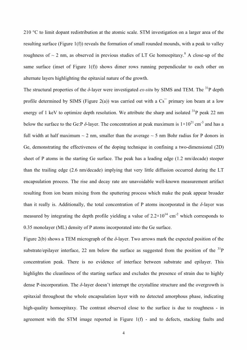
210 °C to limit dopant redistribution at the atomic scale. STM investigation on a larger area of the
resulting surface (Figure 1(f)) reveals the formation of small rounded mounds, with a peak to valley
roughness of ~ 2 nm, as observed in previous studies of LT Ge homoepitaxy.8 A close-up of the
same surface (inset of Figure 1(f)) shows dimer rows running perpendicular to each other on
alternate layers highlighting the epitaxial nature of the growth.
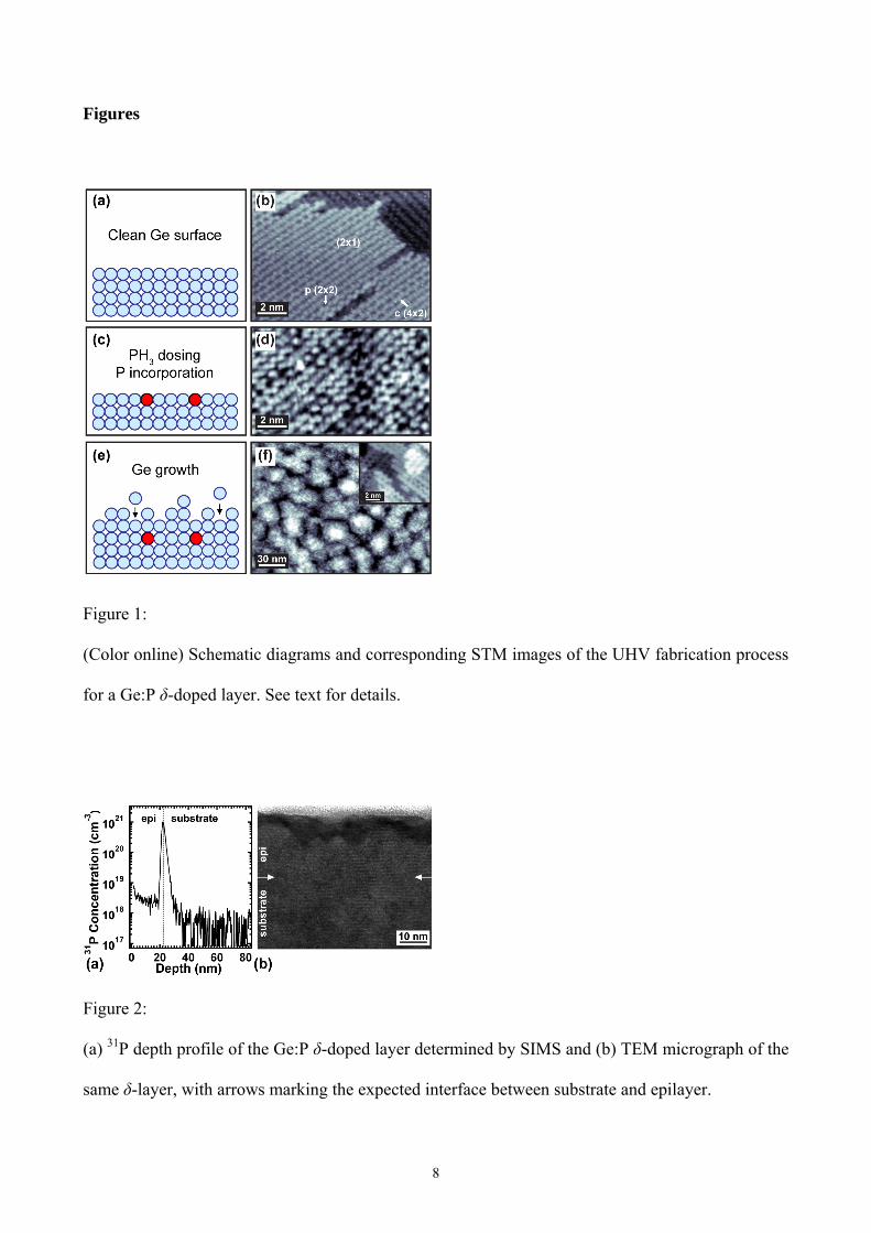
The structural properties of the δ-layer were investigated ex-situ by SIMS and TEM. The 31P depth
profile determined by SIMS (Figure 2(a)) was carried out with a Cs¯ primary ion beam at a low
energy of 1 keV to optimize depth resolution. We attribute the sharp and isolated 31P peak 22 nm
below the surface to the Ge:P δ-layer. The concentration at peak maximum is 1×1021 cm-3 and has a
full width at half maximum ~ 2 nm, smaller than the average ~ 5 nm Bohr radius for P donors in
Ge, demonstrating the effectiveness of the doping technique in confining a two-dimensional (2D)
sheet of P atoms in the starting Ge surface. The peak has a leading edge (1.2 nm/decade) steeper
than the trailing edge (2.6 nm/decade) implying that very little diffusion occurred during the LT
encapsulation process. The rise and decay rate are unavoidable well-known measurement artifact
resulting from ion beam mixing from the sputtering process which make the peak appear broader
than it really is. Additionally, the total concentration of P atoms incorporated in the δ-layer was
measured by integrating the depth profile yielding a value of 2.2×1014 cm-2 which corresponds to
0.35 monolayer (ML) density of P atoms incorporated into the Ge surface.
Figure 2(b) shows a TEM micrograph of the δ-layer. Two arrows mark the expected position of the
substrate/epilayer interface, 22 nm below the surface as suggested from the position of the 31P
concentration peak. There is no evidence of interface between substrate and epilayer. This
highlights the cleanliness of the starting surface and excludes the presence of strain due to highly
dense P-incorporation. The δ-layer doesn’t interrupt the crystalline structure and the overgrowth is
epitaxial throughout the whole encapsulation layer with no detected amorphous phase, indicating
high-quality homoepitaxy. The contrast observed close to the surface is due to roughness - in
agreement with the STM image reported in Figure 1(f) - and to defects, stacking faults and
4

consequent cusps, that originate during the LT growth.8 These, however, do not disturb the P atoms
sheet buried ∼ 20 nm under the surface where the Ge matrix has a high crystal quality, as observed
in the TEM images (see Fig. 2(b)).
The electrical properties of the δ-layers were studied by magnetotransport measurements at 4.2 K
with standard low-frequency lock-in techniques. Trench-isolated Hall bars were defined by a
CHF3/CF4 based dry etch and ohmic contacts to the δ-layer were formed by thermally evaporated
Al.9 All measured Hall bars show ohmic conductivity with a sheet resistance of ρxx = 5.5 kΩ/□. The
Hall resistance ρxy has a linear dependence vs. perpendicular magnetic field B (Figure 3(a)) and
from the slope we calculate an electrically-active sheet carrier concentration of n2D = 4×1013 cm-2.
Comparing this to the total incorporated P density 2.2 × 1014 cm-2 obtained from SIMS, we conclude
that only 20% of the P atoms in the δ-layer are electrically-active. Similar low activations were
reported previously for Si:P δ-layers heavily doped above the solid-solubility limit (SSL) for P in
Si, and were ascribed to the formation of inactive P-related precipitates or dopant vacancy
complexes which are known to reduce electrical activation.10 The same might happen in the Ge:P
layers since the SIMS profile shows a peak concentration of incorporated P of 1×1021 cm-3, well
above the usually quoted SSL of 2×1020 cm-3 for P in Ge.11 We expect to obtain higher activation by
optimizing the dose/incorporation step in order reduce the amount of incorporated P to 0.25 ML
needed for complete substitutional doping.
Despite the low percentage of activation, we achieve a remarkable density of electrically-active P
dopants. We estimate the electrically-active 3D bulk concentration N = 2×1020 cm-3 from N ~ n2D/w,
where w is the 2 nm full width at half maximum of the SIMS 31P peak.12 This value approaches the
solubility limit and is ~ 4 times higher than other electrically-active concentration reported
previously for P-doped Ge layers (~ 5×1019 cm-3).4 From n2D and the zero field sheet resistance
ρxx(0) we calculate the electron mobility μ = 28.3 cm2/Vs, elastic scattering time
τ = 3.5×10⁻¹⁵ s and mean free path l = 1.5 nm. Low μ and l are expected in ultra-dense δ-layers due
to the impurity scattering of the electrons strongly confined in the dopant layer.10 Future attempts to
5

enhance μ and l will include in-situ and/or ex-situ anneal steps to improve the crystal quality after
encapsulation, as demonstrated for Si:P ultra-dense δ-layers.13 Figure 3(b) shows a plot of the
magnetoconductivity ( ) ( )[ ] ( )[ ] 11 0 −− −=Δ xxxx BB ρρσ , where ρxx(B) is the measured longitudinal
resistivity as a function of B. The inverted peak at zero field is due to the weak localization (WL)
that arises from the coherent backscattering of electrons in time-reversed trajectories. Observation
of WL is a clear signature of the 2D nature of transport in these systems and is associated with the
strong confinement of the carriers in the δ-doped layer. For a disordered 2D system of non
interacting electrons the WL correction to the conductivity σ is described by the Hikami formula:14
( )⎥⎥⎦
⎤
⎢⎢⎣
⎡
⎟⎟
⎠
⎞
⎜⎜
⎝
⎛+−⎟
⎟⎠
⎞⎜⎜⎝
⎛+−=
BevBevheB
FFWL
φττψ
τψ
παδσ 222
2
221
221 hh (1)
where α is a phenomenological prefactor expected to be close to 1, Ψ is the digamma function, τφ
the phase relaxation time and vF the Fermi velocity. Together with the experimental data, in Figure
3(b) we report the theoretical fit of Δσ(B) to δσWL(B)−δσWL(0) using α and τφ as fitting parameters.
We found a best fit for α = 0.87 and τφ = 5.6×10⁻¹² s and calculate a phase coherence length lφ =
41.5 nm from φφ ττ22
21
Fvl = . This value is comparable to phase coherence values reported in Si:P δ-
layers with comparable carrier densities.10
In summary, we have demonstrated that P doping at a high concentration is possible in Ge using a
UHV compatible low thermal budget δ-doping technique. These results open up the possibility of
forming reliable n-type source/drain regions in ultra-scaled Ge n-MOSFET. Following our recent
demonstration of UHV-STM nanolithography on hydrogen-terminated Ge,15 we intend to integrate
this δ-doping technique in an STM-based device scheme to fabricate devices in Ge with atomic
scale dopant profiles.
GS acknowledges support from UNSW under the 2009 Early Career Research and Science Faculty
Research Grant scheme. GC is thankful to UNSW for a Visiting Professor Fellowship. MYS
acknowledges an Australian Government Federation Fellowship.
6

References
1International Technology Roadmap for Semiconductors (ITRS) (Semiconductor Industry
Association, Seoul, Korea, 2007).
2 H. Shang, M. Frank, E. P. Gusev, J. O. Chu, S. W. Bedell, K. W. Guarini, and M. Ieong, IBM J.
Res. Dev. 50, 377 (2006).
3Y. Kamata, Materials Today 11, 30 (2008).
4C. O. Chui, L. Kulig, J. Moran, W. Tsai, and K. C. Saraswat, Appl. Phys. Lett. 87, 091909 (2005).
5M. Y. Simmons, F. J. Rueß, K. E. J. Goh, T. Hallam, S. R. Schofield, L. Oberbeck, N. J. Curson,
A. R. Hamilton, M. J. Butcher, R. G. Clark, and T. C. G. Reusch, Mol. Simul. 31, 505 (2005).
6H. J. W. Zandvliet, Phys. Rep. 388, 1 (2003).
7H.-W. Tsai and D.-S. Lin, Surf. Sci. 482–485, 654 (2001).
8K. A. Bratland, Y. L. Foo, J. A. N. T. Soares, T. Spila, P. Desjardins, and J. E. Greene, Phys. Rev.
B 67, 125322 (2003).
9Throughout the whole Hall bar fabrication process the temperature was kept below 180°C in order
to minimize P diffusion.
10K. E. J. Goh, L. Oberbeck, M. Y. Simmons, A. R. Hamilton, and M. J. Butcher, Phys. Rev. B 73,
035401 (2006).
11F. A. Trumbore, Bell Syst Tech. J. 39, 205 (1960).
12This estimate matches N = 2.5×1020 cm-3 that can be calculated from the simple scaling formula
N=(n2D)3/2, valid in the limit of an homogenous semiconductor with same mean distance between
atoms and for an ideal δ-distribution of n2D dopants.
13K. E. J. Goh, Y. Augarten, L. Oberbeck, M. Y. Simmons, Appl. Phys. Lett. 93, 142105 (2008).
14S. Hikami, A. I. Larkin, and Y. Nagaoka, Prog. Theor. Phys. 63, 707 (1980).
15G. Scappucci et al, in manuscript in preparation.
7
Figures
Figure 1:
(Color online) Schematic diagrams and corresponding STM images of the UHV fabrication process
for a Ge:P δ-doped layer. See text for details.
Figure 2:
(a) 31P depth profile of the Ge:P δ-doped layer determined by SIMS and (b) TEM micrograph of the
same δ-layer, with arrows marking the expected interface between substrate and epilayer.
8
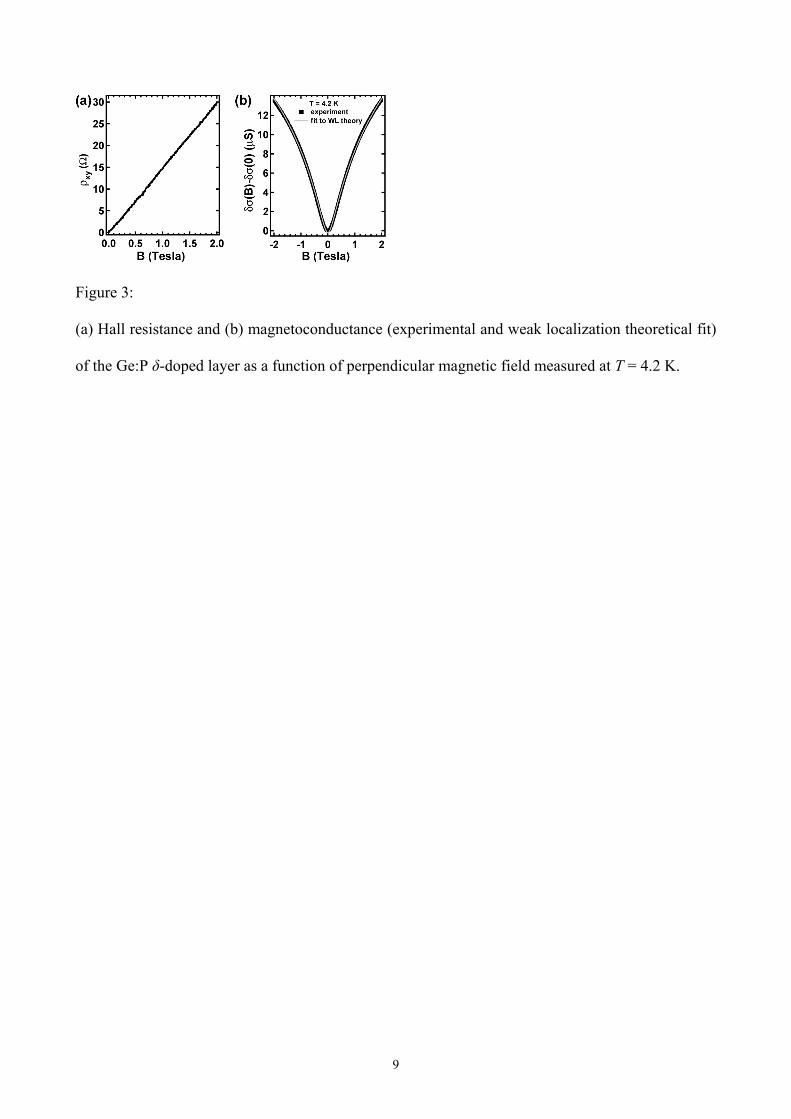
Figure 3:
(a) Hall resistance and (b) magnetoconductance (experimental and weak localization theoretical fit)
of the Ge:P δ-doped layer as a function of perpendicular magnetic field measured at T = 4.2 K.
9