One-dimensional hole gas in germanium/silicon nanowire heterostructures
Effects of point defect healing on phosphorus implanted germanium n+/pjunction and its thermal stabilityJaewoo Shim, Jeong-hun Shin, In-Yeal Lee, Daebeom Choi, Jung Woo Baek et al. Citation: J. Appl. Phys. 114, 094515 (2013); doi: 10.1063/1.4820580 View online: http://dx.doi.org/10.1063/1.4820580 View Table of Contents: http://jap.aip.org/resource/1/JAPIAU/v114/i9 Published by the AIP Publishing LLC. Additional information on J. Appl. Phys.Journal Homepage: http://jap.aip.org/ Journal Information: http://jap.aip.org/about/about_the_journal Top downloads: http://jap.aip.org/features/most_downloaded Information for Authors: http://jap.aip.org/authors

Effects of point defect healing on phosphorus implanted germaniumn1/p junction and its thermal stability
Jaewoo Shim,1 Jeong-hun Shin,1 In-Yeal Lee,1 Daebeom Choi,1 Jung Woo Baek,2
Jonggon Heo,3 Wonkyu Park,3 Jung Woo Leem,4 Jae Su Yu,4 Woo-Shik Jung,5
Krishna Saraswat,5 and Jin-Hong Park1,a)
1Samsung-SKKU Graphene Center and School of Electronics and Electrical Engineering,Sungkyunkwan University, Suwon 440-746, South Korea2School of Mechanical & Aerospace Engineering, Nanyang Technological University, 639798 Singapore3Korea Advanced Nano Fab Center, Suwon 443-270, South Korea4Department of Electronics and Radio Engineering, Institute for Laser Engineering, Kyung Hee University,Yongin 446-701, South Korea5Department of Electrical Engineering, Stanford University, Stanford, California 94305, USA
(Received 12 June 2013; accepted 22 August 2013; published online 6 September 2013)
In this work, the effect of Ge point defect healing process between 550 �C and 650 �C is
investigated, in the aspect of leakage (off) current and junction depth of Ge nþ/p junction diodes
using ECV, TEM, J-V, and SIMS analyses. After 600 �C anneal, off-current density (2� 10�4 A/cm2)
is dramatically reduced due to the defect healing phenomenon that decreases the number of point
defects, subsequently providing a higher on/off-current ratio of 5� 103. In spite of the high healing
temperature, junction diodes seem not to suffer from the deep diffusion of phosphorus (P) in Ge
because those diffuse mostly through VGe. In addition, it is also confirmed that Ti is an appropriate
material in terms of diffusion barrier and diffusivity for Ge nþ/p junction contact metal. VC 2013AIP Publishing LLC. [http://dx.doi.org/10.1063/1.4820580]
I. INTRODUCTION
Germanium (Ge) is one of the attractive candidates for
next generation complementary metal oxide semiconductor
(CMOS) due to its higher carrier mobility1 and lower proc-
essing temperature2,3 compared to silicon (Si). However,
conventional ion implantation process for source/drain (S/D)
junction formation causes severe crystal damage and it con-
sequently increases the number of point defects consisting of
Ge vacancy (VGe) and self-interstitial (Gei) atoms.4 Since
these point defects work as recombination trap centers in Ge,
it induces generation current (IG) and thereby increases the
total junction leakage current. In addition, fast diffusion of
n-type dopants through VGe is hinders shallow S/D junction
fabrication.5–7 Although rapid thermal annealing (RTA),8,9
laser annealing (LA),10,11 metal induced dopant activation
(MIDA)12,13 techniques have been developed to achieve
shallow and high quality junction interface in Ge, the
obtained S/D junctions are still not free from the leakage and
fast diffusion problems due to unhealed point defects.
Recently, several research groups have proposed hydrogen
and fluorine-based passivation methods14,15 to reduce the
number of VGe, and we also have reported the healing phe-
nomenon of point defects in Ge by high temperature and
long annealing process.16 These studies confirm Ge point
defects reduction through transmission electron microscopy
(TEM), deep level transient spectroscopy (DLTS), or spread-
ing resistance profiling (SRP) analysis. In this paper, the
healing phenomenon of Ge point defects is not only con-
firmed by the high temperature—long anneal process but its
effect on leakage (off) current and junction depth in Ge nþ/p
junction diodes is also investigated through electrochemical
capacitance-voltage (ECV), transmission electron micros-
copy (TEM), current density-voltage (J-V), and secondary
ion mass spectroscopy (SIMS) analyses. In addition, the
electrical degradation of optimally healed Ge nþ/p junction
diodes with Ni or Ti contact is analyzed according to post-
fabrication process temperatures between 250 �C and 350 �C.
II. EXPERIMENTAL
About 2.6 lm thick high quality crystalline intrinsic Ge
(p-type: �5� 1014 cm�3) layer was grown heteroepitaxially
on a p-type Si substrate using multistep hydrogen annealing
(MHAH) growth method.17 For the first part of the experi-
ment, 20 nm thick SiO2 layer was deposited on the Ge layer
in a low-pressure chemical vapor deposition (LPCVD) sys-
tem to avoid surface damage by ion implantation. In order to
create intentional Ge point defects (VGe and Gei), Ge ions
with dose of 1� 1014 cm�2 were then implanted into the Ge
region at 180 keV. The implanted samples were thermally
annealed at 500 �C, 600 �C, and 700 �C for 1 h in N2 ambient
using a thermal furnace and ECV measurement was per-
formed on the samples to confirm the healing phenomenon
of VGe according to annealing temperature. For the second
experimental part, 20 nm thick Al2O3 layer was deposited on
the Ge layer by an atomic layer deposition (ALD) system to
prevent surface damage by ion implantation and also to pas-
sivate the Ge surface. Phosphorus (P) ions were then
implanted into the Ge layer at 60 keV with 1015 cm�2 dose to
achieve nþ Ge region. The samples were annealed at 550 �C,
600 �C, and 650 �C for 1 h in a N2 ambient to activate P atoms
as well as to heal VGe, followed by titanium (Ti)/aluminum
a)Author to whom correspondence should be addressed. Electronic mail:
0021-8979/2013/114(9)/094515/6/$30.00 VC 2013 AIP Publishing LLC114, 094515-1
JOURNAL OF APPLIED PHYSICS 114, 094515 (2013)

(Al) deposition with a metal shadow mask to form contact
electrodes. J-V measurement was finally performed on the
fabricated junction diodes together with TEM, SIMS, and
ECV analyses to investigate the effect of VGe healing on
leakage current and junction depth of the junction diodes.
For the third experimental part to study the thermal stability
of the diodes, sample with nickel (Ni) instead of Ti as a con-
tact metal was additionally prepared and was compared with
Ti contact junction diodes through J-V and SIMS analyses
after performing post-fabrication anneal at 250 �C, 300 �C,
and 350 �C for 10 s in a RTA system.
III. RESULTS AND DISCUSSION
Crystal damages induced during ion implantation process
are known to form Frenkel pairs consisting of VGe and Gei, as
shown in (i) of Fig. 1(a). After going through high tempera-
ture annealing process, (ii) the Frenkel pairs are eliminated
due to recombination of Gei and VGe and (iii) consequently
point defects are healed. In order to confirm the defect healing
phenomenon according to annealing temperature, defects are
intentionally generated by implanting Ge ions into the Ge
layer. These samples are then annealed at various tempera-
tures (500 �C, 600 �C, and 700 �C). Fig. 1(b) shows the carrier
concentrations of the annealed Ge samples, which are esti-
mated by ECV analysis. Because it is difficult to measure the
precise carrier concentration near surface region through ECV
method, the concentration data were extracted at the 300 nm
below surface where the tail region of implanted Ge atoms is
located and the carrier concentration is uniformly distributed
as a function of depth. In the case of Ge implantation with
high energy of 180 keV, the tail is observed even below 1 lm
deep region without additional annealing process. In addition,
VGe and Gei are uniformly distributed from surface to bulk
regions after the long time annealing process due to the high
diffusivity values of Gei (1� 10�5 cm2/s at 600 �C) and VGe
(4.8� 10�8 cm2/s at 600 �C),18 consequently making the
Frenkel pairs recombination to occur at both surface and bulk
regions. Very high p-type concentration was observed in the
as-implanted sample due to VGe with acceptor level at 0.20 eV
above the top of the Ge valence band.19 However, this con-
centration reduced with higher annealing temperatures owing
to the recombination of VGe and Gei. Although there are also
Gei atoms with donor level at 0.04 eV bottom of the conduc-
tion band19 or 0.15 eV above the top of the valence band,20
the measured carrier concentration is presented as p-type
because Gei moves deeper from the junction and VGe with
acceptor charge level in the Ge energy band resides near the
surface.21,22
As shown in Fig. 2(a), J-V characteristics of the Ge nþ/p
junction diodes annealed at 550 �C, 600 �C, and 650 �C are
measured to investigate the effect of point defect healing phe-
nomenon on the off-current. The 550 �C and 650 �C annealing
range for Ge nþ/p junctions were selected because, (1) 500 �Cor above anneal is normally needed to activate n-type dopants
fully in Ge23 and (2) effective defect healing phenomenon
was observed above 600 �C (Fig. 1). We also note that the J-V
characteristics are analyzed through the previously obtained
VGe concentration data because it is hard to estimate accu-
rately the concentration of VGe created after P implantation by
ECV. On/off-current ratio and on-current density were
extracted at |V|¼ 1 V in the J-V curves and are plotted in Fig.
2(b) as a function of annealing temperature. Based on the suc-
ceeding SIMS data (see Fig. 4(a)), the diffusivity of P atoms
was estimated to be 7.09� 10�16 cm2/s at 550 �C, which was
much slower than that of VGe (4.12� 10�8 cm2/s).18 A num-
ber of VGe left near surface region due to preferential momen-
tum transfer22 are also expected to be distributed uniformly
from surface to bulk region by its high diffusivity at each
annealing temperatures. Since the VGe which is not healed af-
ter annealing at 550 �C acts as a recombination trap center in
Ge nþ/p junction interface, a high generation current (IG)
was observed in the junction sample annealed at 550 �C.
Above 600 �C, because the number of VGe was significantly
decreased, the annealed junction sample showed dramatic
decrease of off-current density while maintaining on-current
density, which subsequently provided a higher on/off-current
ratio of 5� 103. However, VGe working as a recombination
FIG. 1. (a) Schematic diagram for the defect healing phenomenon.
(b) Carrier concentrations extracted through ECV measurement at 300 nm
deep region from surface of the Ge implanted samples non-annealed and
annealed at 500 �C, 600 �C, and 700 �C.
094515-2 Shim et al. J. Appl. Phys. 114, 094515 (2013)

trap still seemed to remain in the junction interface, making
the off-current to increase as a function of reverse voltage
bias. Since the number of VGe was continuously reduced by
the point defect healing process with increased annealing tem-
perature (Fig. 1(b)), it can be expected from the junction sam-
ple annealed at 650 �C that (1) most of the point defects are
healed, (2) IG is reduced through the increased carrier lifetime,
and (3) off-current density is finally saturated. In addition,
because the hole concentration is reduced by the number of
VGe with acceptor charge level, diffusion current (IDiff) which
is inversely proportional to the concentration of lightly doped
p-type region seems to increase. As a result, when compared
to the junction sample annealed at 600 �C, saturated off-
current density was obtained due to the reduced IG in the
650 �C annealed junction, but the total leakage current density
was increased through the increase of IDiff. Fig. 3 shows the
cross-sectional TEM images of Ge nþ/p junctions; (a) non-
annealed and (b) annealed at 600 �C. Although the ion implan-
tation process of n-type dopants (P ions) initially damages the
Ge surface region up to 64 nm in depth, this region seems to
recrystallize after 600 �C anneal, indicated by the interface
between (I) damaged and (II) non-damaged regions shifting
towards the Ge surface. Even though the implanted (damaged)
region does not seem to have a crystal lattice structure, it is
hard to conclude that the region is fully amorphized since the
dose of implanted P ions is not sufficient for a full amorphiza-
tion of the region (1015 cm�2). In addition, we also note that
the TEM images of as-implanted and recrystallized samples
(at 600 �C) only show the highly damaged regions, where the
lowly damaged tail regions are not shown.
Fig. 4(a) shows the chemical concentrations (SIMS pro-
files) of P atoms in the 600 �C annealed sample as a function
of junction depth and their fitted profiles which consist of
Gaussian (region I) and Error (region II) functions. The dif-
ference of crystal quality at surface and deep junction
regions induced by an ion implantation process makes out-
diffusivity of P atoms to have slightly different values when
compared to in-diffusivity. In the region I showing Gaussian
distribution, P atoms were piled up near the surface by the
out-diffusion and surface back-scattering phenomena.
However, it was also observed that P atoms diffusing toward
the bulk region followed an Error function distribution
(region II), where the P atoms piled-up in region I served as
an infinite source. In order to investigate these two different
dopant distributions in more detail, diffusivity and pile-up ra-
tio (piled-up concentration in region I/total concentration)
extracted from Gaussian fitted curve in the region I were first
plotted as a function of annealing temperature in Fig. 4(b).
As the annealing temperature increases, the pile-up ratio
increased due to enhanced diffusion phenomenon at higher
annealing temperature, indicating that more number of P
atoms flowed into the region I. As shown in Fig. 4(c), activa-
tion energy (EA) and pre-exponential factor were also esti-
mated to be respectively 1.09 eV and 3.12� 10�9 cm2/s in
the region II by fitting the distributed P atoms through the
least square method. Although similar diffusivity was
reported at 600 C by Chui et al. (4.91� 10�14 cm2/s),8 it is
predicted that RTA process did not provide enough thermal
energy and time to heal VGe and consequently high pre-
exponential factor (4.38� 10�2 cm2/s) was observed. In addi-
tion, Carroll et al.7 and Koffel et al.24 also reported similar high
pre-exponential factors (1.85� 10�2 cm2/s and 10�2 cm2/s). It
is thought that in these works much more number of VGe
FIG. 3. Cross-sectional TEM images of the Ge nþ/p junctions (a) non-
annealed and (b) annealed at 600 �C. Region I and II respectively indicate
damaged and non-damaged regions by an ion implantation process.
FIG. 2. (a) J-V characteristics of the Ge nþ/p junction diodes annealed (or
activated) at 550 �C, 600 �C, and 650 �C for 1 h. (b) On/off-current ratio and
on-current density of the junction diodes as a function of annealing tempera-
ture at |V|¼ 1 V.
094515-3 Shim et al. J. Appl. Phys. 114, 094515 (2013)
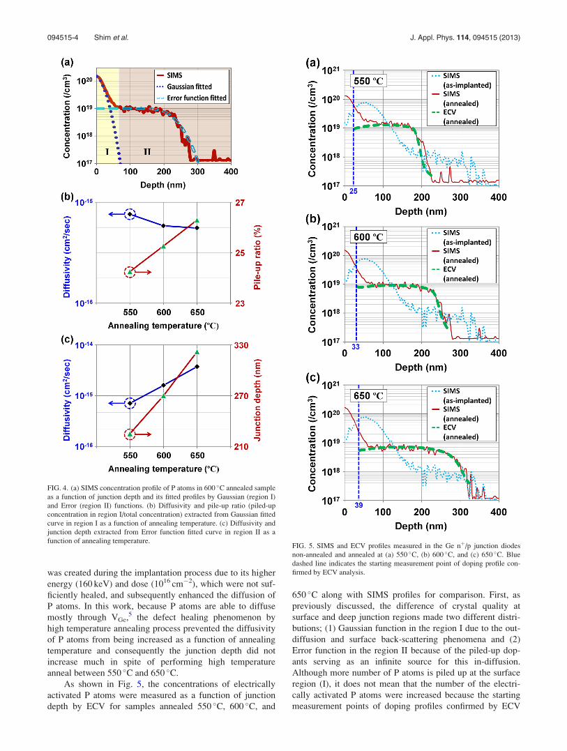
was created during the implantation process due to its higher
energy (160 keV) and dose (1016 cm�2), which were not suf-
ficiently healed, and subsequently enhanced the diffusion of
P atoms. In this work, because P atoms are able to diffuse
mostly through VGe,5 the defect healing phenomenon by
high temperature annealing process prevented the diffusivity
of P atoms from being increased as a function of annealing
temperature and consequently the junction depth did not
increase much in spite of performing high temperature
anneal between 550 �C and 650 �C.
As shown in Fig. 5, the concentrations of electrically
activated P atoms were measured as a function of junction
depth by ECV for samples annealed 550 �C, 600 �C, and
650 �C along with SIMS profiles for comparison. First, as
previously discussed, the difference of crystal quality at
surface and deep junction regions made two different distri-
butions; (1) Gaussian function in the region I due to the out-
diffusion and surface back-scattering phenomena and (2)
Error function in the region II because of the piled-up dop-
ants serving as an infinite source for this in-diffusion.
Although more number of P atoms is piled up at the surface
region (I), it does not mean that the number of the electri-
cally activated P atoms were increased because the starting
measurement points of doping profiles confirmed by ECV
FIG. 4. (a) SIMS concentration profile of P atoms in 600 �C annealed sample
as a function of junction depth and its fitted profiles by Gaussian (region I)
and Error (region II) functions. (b) Diffusivity and pile-up ratio (piled-up
concentration in region I/total concentration) extracted from Gaussian fitted
curve in region I as a function of annealing temperature. (c) Diffusivity and
junction depth extracted from Error function fitted curve in region II as a
function of annealing temperature.FIG. 5. SIMS and ECV profiles measured in the Ge nþ/p junction diodes
non-annealed and annealed at (a) 550 �C, (b) 600 �C, and (c) 650 �C. Blue
dashed line indicates the starting measurement point of doping profile con-
firmed by ECV analysis.
094515-4 Shim et al. J. Appl. Phys. 114, 094515 (2013)

analysis were, respectively, 25 nm, 33 nm, and 39 nm at
550 �C, 600 �C, and 650 �C. Since depletion width indicating
the starting measurement point is inversely proportional to a
carrier concentration, lower electrically activated P concen-
tration is expected at the surface region as the annealing tem-
perature increases. In addition, we also confirmed that ECV
profiles are almost coincide with SIMS data at the deep junc-
tion region, indicating that most of P atoms at the region II
were successfully activated by high thermal energy supplied
above 550 �C.
Finally, in order to investigate thermal stability of the
healed junction diodes, Ni and Ti were selected as a contact
metal for the 600 �C annealed (or healed) junction diode
samples. These two diodes were analyzed and compared af-
ter going through the post-fabrication anneal at 250 �C,
300 �C, and 350 �C for 10 s. Fig. 6 shows (a) J-V characteris-
tics of the Ge nþ/p junction diodes with Ti contact and (b)
on/off-current ratio / on-current density data extracted from
the J-V curves. After the 250 �C short time annealing pro-
cess, off- and on-current densities are decreased due to addi-
tional crystallization induced by Ti13 and high resistivity of
Ti germanide phase formed at 250 �C,25 respectively. As
shown in Fig. 8(a), small amount of Ti atoms seems to
diffuse into the junction at this temperature because of its
relatively low diffusivity in Ge, forming larger grains in the
junction interface through small number of heterogeneous
nuclei during metal-induced crystallization (MIC),13,26
which subsequently reduces IG. We previously reported a
similar phenomenon in the Ge nþ/p junction diodes activated
by cobalt (Co) at 360 �C.12 However, as RTA temperature
increases up to 350 �C, the off-current density was dramati-
cally increased because more number of Ti atoms worked as
recombination centers in Ge is placed in the junction inter-
face. The SIMS intensity of Ti in the 350 �C RTA processed
sample seems to be increased about 100 times in Fig. 8(a)
when compared to the 250 �C sample. In addition, on-current
density increased above 300 �C annealing since another Ti
germanide phase with relatively low resistivity was achieved
at the temperatures.25 Similarly, in Fig. 7 showing (a) J-V
characteristics of the Ge nþ/p junction diodes with Ni con-
tact and (b) on/off-current ratio / on-current density data
extracted from the J-V curves, it is confirmed that off- and
on-current density were respectively decreased and increased
after annealing above 300 �C. The increase of on-current
density seems to be attributed to Ni germanide formation
reducing the contact resistance. However, because of rela-
tively faster diffusion of Ni atoms in Ge compared to Ti,12,27
increase of off-current density and decrease of on/off-current
ratio are expected even at 250 �C. In fact, the on/off-current
ratio continuously reduced as the RTA temperature
increased. As shown in Fig. 8(b), degree of Ni diffusion at
250 �C is similar to that of 350 �C, indicating that large
amounts of Ni traps are already located in the junction inter-
face even after 250 �C low temperature anneal. Therefore, it
FIG. 6. (a) J-V characteristics of the Ge nþ/p junction diodes with Ti con-
tact, which are non-annealed and annealed at 250 �C, 300 �C, and 350 �C for
10 s. (b) On/off-current ratio and on-current density data extracted from the
J-V curves at |V|¼ 1 V.
FIG. 7. (a) J-V characteristics of the Ge nþ/p junction diodes with Ni con-
tact, which are non-annealed and annealed at 250 �C, 300 �C, and 350 �C for
10 s. (b) On/off-current ratio and on-current density data extracted from the
J-V curves at |V|¼ 1 V.
094515-5 Shim et al. J. Appl. Phys. 114, 094515 (2013)

is thought that Ti which can work as diffusion barrier28 and
diffuse itself slowly into Ge junction is an appropriate con-
tact metal in most of Ge nþ/p junctions fabricated by this
defect healing process as well as the previously mentioned
techniques, such as RTA, LA, and MIDA.
IV. CONCLUSION
In this work, we not only confirmed the healing phe-
nomenon of Ge point defects by high temperature—long
time anneal but also investigated its effect on off-current and
junction depth in Ge nþ/p junction diodes through ECV,
TEM, J-V, and SIMS analyses. After annealing above
600 �C, a dramatic decrease in off-current density was
observed, maintaining on-current density and subsequently
providing a higher on/off-current ratio of 5� 103, because
the number of VGe significantly decreased by defect healing.
In spite of the high temperature anneal between 550 �C and
650 �C, the junction diodes seemed not to suffer from deep
diffusion problem because P atoms diffuse mostly through
VGe.5 In addition, electrical degradation of optimally healed
Ge nþ/p junction diodes with Ni or Ti contact according to
post-fabrication process temperature between 250 �C and
350 �C was analyzed. The relatively fast diffusion of Ni atoms
in Ge when compared to Ti12,27 increased the off-current
density and also decreased on/off-current ratio at 250 �C, and
this on/off-current ratio continuously reduced with increasing
RTA temperature. As a result, it was confirmed that Ti is the
appropriate material in terms of diffusion barrier and diffusiv-
ity for contact metal for Ge nþ/p junctions.
ACKNOWLEDGMENTS
This research was supported by (1) Basic Science
Research Program through the National Research Foundation
of Korea (NRF) funded by the Ministry of Education, Science,
and Technology (NRF-2011-0007997) and (2) International
Collaborative R&D program of the Korea Institute of Energy
Technology Evaluation and Planning (KETEP) grant funded
by the Korea government Ministry of Knowledge Economy
(No. 2011-8520010030).
1C. O. Chui, S. Ramanathan, B. B. Triplett, P. C. McIntyre, and K. C.
Saraswat, IEEE Electron Device Lett. 23, 473 (2002).2Z. Meng, Z. Jin, B. A. Gururaj, P. Chu, H. S. Kwok, and M. Wong,
J. Electrochem. Soc. 144, 1423 (1997).3J.-H. Park, D. Kuzum, W.-S. Jung, and K. C. Saraswat, IEEE Electron
Device Lett. 32, 234 (2011).4P. Ehrhart and H. Zillgen, J. Appl. Phys. 85, 3503 (1999).5A. Chroneos, H. Bracht, R. W. Grimes, and B. P. Uberuaga, Appl. Phys.
Lett. 92, 172103 (2008).6Y. S. Suh, M. S. Carroll, R. A. Levy, A. Sahiner, and C. A. King, Mater.
Res. Soc. Symp. Proc. 809, B8.11 (2004).7M. S. Carroll and R. Koudelka, Semicond. Sci. Technol. 22, S164 (2007).8C. O. Chui, K. Gopalakrishnan, P. B. Griffin, J. D. Plummer, and K. C.
Saraswat, Appl. Phys. Lett. 83, 3275 (2003).9A. Satta, T. Janssens, T. Clarysse, E. Simoen, M. Meuris, A. Benedetti, I.
Hoflijk, B. D. Jaeger, C. Demeurisse, and W. Vandervorst, J. Vac. Sci.
Technol. B 24, 494 (2006).10P. Tsouroutas, D. Tsoukalas, A. Florakis, I. Zergioti, A. A. Serafetinides,
N. Cherkashin, B. Marty, and A. Claverie, Mater. Sci. Semicond. Proc. 9,
644 (2006).11S. Heo, S. Baek, D. Lee, M. Hasan, H. Jung, J. Lee, and H. Hwang,
Electrochem. Solide-State Lett. 9, G136 (2006).12J.-H. Park, M. Tada, P. Kapur, and K. C. Saraswat, Appl. Phys. Lett. 93,
183512 (2008).13J.-H. Park, M. Tada, W.-S. Jung, H.-S. P. Wong, and K. C. Saraswat,
J. Appl. Phys. 106, 074510 (2009).14A. J. Tavendale and S. J. Pearton, J. Appl. Phys. 54, 3213 (1983).15W.-S. Jung, J.-H. Park, A. Nainani, D. Nam, and K. C. Saraswat, Appl.
Phys. Lett. 101, 072104 (2012).16J. Shim, I. Song, W.-S. Jung, J. Nam, J. W. Leem, J. S. Yu, D. E. Kim, W.
J. Cho, Y. S. Kim, D.-H. Jun, J. Heo, W. Park, J.-H. Park, and K. C.
Saraswat, IEEE Electron Device Lett. 34, 15 (2013).17H.-Y. Yu, S.-I. Cheng, J.-H. Park, A. K. Okyay, M. C. Onbasli, B. Ercan,
Y. Nishi, and K. C. Saraswat, Appl. Phys. Lett. 97, 063503 (2010).18J. W. Kang, Y. G. Choi, J. H. Lee, S. H. Lee, and H. J. Oh, Mol. Simul.
35, 234 (2009).19H. Haesslein, R. Sielemann, and C. Zistl, Phys. Rev. Lett. 80, 2626 (1998).20A. Janotti, R. Baierle, A. J. R. da Silva, R. Mota, and A. Fazzio, Physica B
273–274, 575 (1999).21M. D. Giles, J. Electrochem. Soc. 138, 1160 (1991).22P. Pellegrino, P. Leveque, J. Wong-Leung, C. Jagadish, and B. G.
Svensson, Appl. Phys. Lett. 78, 3442 (2001).23M. Koike, Y. Kamata, T. Ino, D. Hagishima, K. Tatsumura, M. Koyama,
and A. Nishiyama, J. Appl. Phys. 104, 023523 (2008).24S. Koffel, R. J. Kaiser, A. J. Bauer, B. Amon, P. Pichler, J. Lorenz, L.
Frey, P. Scheiblin, V. Mazzocchi, J.-P. Barnes, and A. Claverie,
Microelectron. Eng. 88, 458 (2011).25Q. Z. Hong, K. Barmak, and F. M. d’Heurle, Appl. Phys. Lett. 62, 3435 (1993).26J.-H. Park, M. Tada, P. Kapur, H. Peng, and K. C. Saraswat, J. Appl. Phys.
104, 064501 (2008).27S. Gaudet, J. Vac. Sci. Technol. A 24, 474 (2006).28M. Mandl, H. Hoffmann, and P. Kucher, J. Appl. Phys. 68, 2127 (1990).
FIG. 8. SIMS profiles of (a) Ti and (b) Ni in the Ge nþ/p junction diode sam-
ples with Ti or Ni contact, which are annealed at 250 �C and 350 �C for 10 s.
094515-6 Shim et al. J. Appl. Phys. 114, 094515 (2013)
Copyright © 2022 FDOKUMEN