Electrical Characterization of Germanium Nanowires Using a ...
Upload
independentCategory
view
1download
0
1
One-Dimensional Hole Gas in Germanium/Silicon Nanowire Heterostructures
Wei Lu†§, Jie Xiang†§, Brian P. Timko†, Yue Wu† & Charles M. Lieber*†‡
†Department of Chemistry and Chemical Biology, Harvard University, Cambridge, MA, 02138,
USA. ‡Division of Engineering and Applied Sciences, Harvard University, Cambridge, MA
02138, USA.
§These authors contributed equally to this work.
*To whom correspondence should be addressed. E-mail: [email protected].
________________________________________________
Corresponding author: Charles M. Lieber, Department of Chemistry and Chemical Biology,
Harvard University, Cambridge, MA 02138; Tel: 617-496-3169; Fax: 617-496-5442; Email:
2
Abstract
Two-dimensional electron and hole gas systems, enabled through band structure design
and epitaxial growth on planar substrates, have served as key platforms for fundamental
condensed matter research and high performance devices. The analogous development of one-
dimensional (1D) electron or hole gas systems through controlled growth on 1D nanostructure
substrates, which could open up opportunities beyond existing carbon nanotube and nanowire
systems, has not been realized. Here we report the synthesis and transport studies of a 1D hole
gas system based on a free-standing germanium/silicon (Ge/Si) core/shell nanowire
heterostructure. Room temperature electrical transport measurements show clearly hole
accumulation in undoped Ge/Si nanowire heterostructures, in contrast to control experiments on
single component nanowires. Low-temperature studies show well controlled Coulomb blockade
oscillations when the Si shell serves as a tunnel barrier to the hole gas in the Ge channel.
Transparent contacts to the hole gas also have been reproducibly achieved by thermal annealing.
In such devices, we observe conductance quantization at low temperatures, corresponding to
ballistic transport through 1D subbands, where the measured subband energy spacings agree
with calculations for a cylindrical confinement potential. In addition, we observe a “0.7
structure”, which has been attributed to spontaneous spin polarization, suggesting the
universality of this phenomenon in interacting 1D systems. Lastly, the conductance exhibits little
temperature dependence, consistent with our calculation of reduced backscattering in this 1D
system, and suggests that transport is ballistic even at room temperature.
3
Carbon nanotubes and semiconductor nanowires have attracted considerable attention as
1D structures for fundamental studies and also as potential building blocks for nanodevices (1-3).
Current synthetic methods can reproducibly yield nanotubes and nanowires with diameters of a
few nanometers (4,5), comparable to the de Broglie wavelength of the carriers. In this regime,
quantum confinement may affect significantly transport through these materials, thus making
them model platforms to study and utilize potentially unique properties of 1D systems (6,7).
Indeed, ballistic transport and conductance quantization have been observed in metallic (8) and
semiconducting carbon nanotubes (9,10). Similar effects have not been observed in
semiconductor nanowires, although the ability to vary size, material composition and electronic
properties of semiconductor nanowires in a controlled manner (2,3) offers substantial potential
for creating designed 1D systems.
Band structure engineering has been widely used in the past to yield interesting planar
systems, including two-dimensional electron gases in GaAs/AlGaAs heterostructures (11) and
two-dimensional hole gases in Ge/SiGe heterostructures (12). 2D electron and 2D hole gases
have been central to mesoscopic physics (13) and have lead, for example, to the discovery of
conductance quantization in quantum point contacts (14) and realization of artificial atoms in
quantum dots (15). We use this underlying concept from 2D to design a 1D hole gas system
based on a Ge/Si core/shell nanowire heterostructure. Because there is ~500 meV valence band
offset (12,16) between the Ge core and Si shell in this heterostructure, free holes will accumulate
in the Ge channel when the Fermi level lies below the valance band edge of the Ge core. We
have demonstrated that transparent contacts to the hole gas can be achieved as a result of the
band line-up, and obtained long carrier mean free path by eliminating scattering from dopants.
With these improvements, we have observed ballistic transport through devices up to a few
hundred nanometers in length both at low temperature and room temperature.
4
Materials and Methods
Ge/Si nanowire growth. Gold nanoclusters of 5 nm, 10 nm and 15 nm diameters (Ted Pella,
Inc., Redding, CA) were first deposited on oxidized silicon wafers and placed in a quartz tube
furnace. Ge nanowire core growth was initiated by nucleation at 315 °C for 1 minute using 10%
GeH4 in H2 (30 sccm) and H2 (200 sccm) at 300 torr, followed by axial elongation at 280 °C for
15 minutes and 100 torr. The i-Si shell was deposited within the same reactor immediately
following Ge core growth at 450 °C for 5~10 minutes using SiH4 (5 sccm) at 5 torr. The growth
rates for the i-Ge core and i-Si shell were ca. 1 µm/min and 0.5 nm/min, respectively. For the
control experiments, i-Ge nanowires were grown using the same procedure as the Ge core, and
i-Si nanowires were grown at 435 °C for 20 min using SiH4/H2 (6/60 sccm) at 60 torr.
Back-gated devices. Nanowires were dispersed in ethanol from growth substrates by sonication,
and then deposited on degenerately doped Si substrates with 50 nm thermal oxide layer (n-type,
resistivity <0.005 Ω-cm, Nova Electronics Materials, Carrollton, TX). Electron beam
lithography and metal deposition were used to define Ni source/drain electrodes (50 nm thick).
To make contacts to the Ge channel, the devices were annealed at 300 °C for 15 seconds in
forming gas (N2/H2, 90/10%) (Heatpulse 610, Metron Technology, San Jose, CA).
Top-gated devices. Atomic layer deposition was used to deposit Al2O3 dielectric conformally on
Ge/Si nanowire devices prepared in the same way as the back-gated devices. Deposition was
carried out at 200 °C using a cycle consisting of 1 s water vapor pulse, 2 s N2 purge, 1 s trimethyl
aluminum, and 2 s N2 purge; 50 cycles were used to yield a thickness of 6 nm. The top gate was
then defined by electron beam lithography, followed by Cr/Au (5/50 nm) deposition.
Electrical transport measurements. Room temperature measurements were performed in
vacuum at a pressure below 4101 −× torr using a cryogenic probe station (TTP-4, Desert

5
Cryogenics, Tucson, AZ). Low temperature measurements were carried out using both the probe
station and a He-4 cryostat (Oxford Instruments, Abingdon, U.K.). The differential conductance
G was measured with a lock-in amplifier (SR 830, Stanford Research Systems, Sunnyvale, CA)
using an 11 Hz ac excitation of 200 µV superimposed on a dc bias voltage.
Results and Discussion
The Ge/Si core/shell (Fig. 1A) nanowires were grown using a reported approach (17),
except that both the Ge core and Si shell were not doped. This difference is critical for our
studies since it eliminates scattering from ionized dopants in the 2-5 nm thick Si shell adjacent to
the Ge channel. A thin Si shell was used in our studies to facilitate electrical contact to the Ge
channel, and to reduce the likelihood of dislocations in the shell. The valence band offset of ca.
500 meV between Ge and Si at the heterostructure interface (12,16) serves as a confinement
potential for the quantum well, and free holes will accumulate in the Ge channel when the Fermi
level lies below the valance band edge of the Ge core (Fig. 1B). High-resolution transmission
electron microscopy studies of the Ge/Si nanowires (Fig. 1C) show clearly the core (dark)/shell
(light) structure. The lattice fringes and sharp interface between Ge and Si show that the
core/shell structure is epitaxial, and is consistent with cross-sectional elemental mapping results.
Lower resolution images also indicate that dislocations are not present in these structures. The
clean, epitaxial interface in these nanowire heterostructures should produce a smooth
confinement potential along the channel. The pseudomorphic strain in the epitaxial core and
shell materials is relaxed along the radial direction (17), and this will yield a type II staggered
band alignment (12). The light hole and heavy hole bands are expected to split due to the effects
of strain and confinement (12).
6
Electrical transport measurements were made on Ge/Si nanowire devices with
lithographically-patterned nickel source/drain electrodes and capacitively coupled back-gate
electrodes. A brief annealing process was performed after the source/drain fabrication to
facilitate contact to the inner Ge channel. Room-temperature current versus source-drain voltage
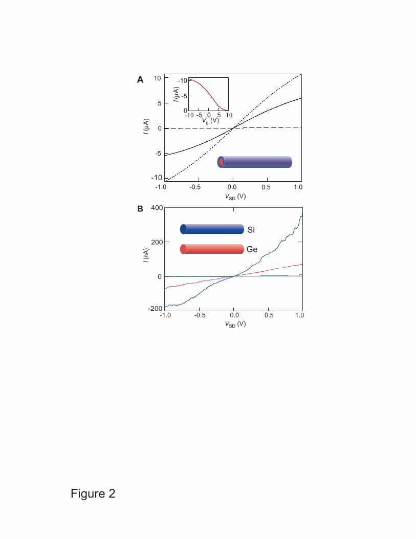
(I-VSD) data recorded on a heterostructure with a 10 nm Ge core diameter (Fig. 2A) exhibit a
substantial current at zero gate voltage (Vg = 0), and a decrease in current as Vg is increased from
-10 to 10 V. These results show that the device behaves as a p-type depletion mode field-effect
transistor (p-FET), and thus confirm the accumulation of hole charge carriers. Because both the
Ge core and the Si shell are un-doped, the existence of a hole gas is a result of the band line-up
as illustrated in Fig. 1B, where the Fermi level is pinned below the Ge valance band edge, due to
the combined effect of work function, band offset and interface states (18). To further probe this
phenomenon, we performed control experiments on intrinsic Si (i-Si) and intrinsic Ge (i-Ge)
nanowires. Transport measurements (Fig. 2B) show that both the i-Si and i-Ge nanowires are
enhancement mode p-FETs with no carriers at Vg=0. The i-Ge nanowire data thus contrast that
obtained for the Ge/Si core/shell structure even though the i-Ge nanowires were grown under
identical conditions to the Ge core in the heterostructure.
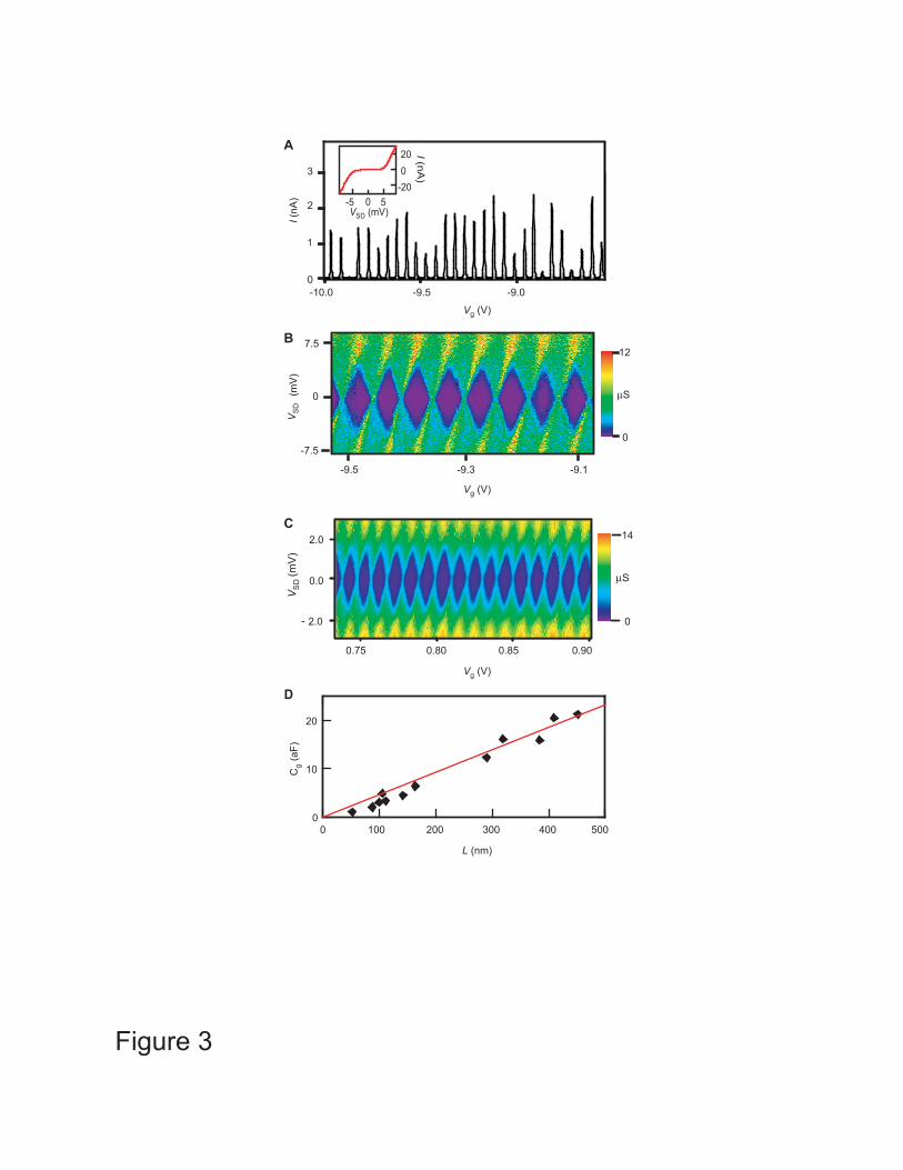
For the Ge/Si core/shell nanowire devices fabricated without the annealing process,
carriers need to tunnel through the non-conducting Si layer, which appear as barriers in transport
data recorded at low temperatures (inset, Fig. 3A). The Ge/Si devices prepared with tunnel
barriers at the contacts show periodic oscillations in I as a function of Vg (Fig. 3A); these are
Coulomb blockade oscillations and the device behaves as a single-electron transistor (SET) (19).
From the period of the current oscillations in Fig. 3A, we estimate the gate capacitance, Cg, to be
3.2 aF for this 112 nm long device. In Fig. 3B, we plot the differential conductance G = dI/dVSD
vs. VSD and Vg for the same device. These data exhibit well-defined Coulomb diamonds as
7
expected for transport through a single SET (19). In Fig. 3C we show G-VSD-Vg for another 385
nm long device with Cg = 15.8 aF, which also shows well-defined Coulomb diamonds
characteristics of transport through a single SET. To verify that the tunnel barriers defining the
SET are not caused by defects inside the nanowire, which break the nanowire into multiple
islands (20), and are often observed in lithographically defined wires (21), we plot (Fig. 3D) the
measured gate capacitance Cg as a function of the source-drain separation L (measured from
SEM images). Notably, the measured Cg agrees well for L > 100 nm with the capacitance
calculated using a cylinder-on-plane model )/(cosh
21
0
rhLCg −=
πεε , where h = 50 nm is the oxide
thickness, r is the radius of the Ge core, and ε is the dielectric constant. For L < 100 nm, the
measured Cg is generally smaller than that predicted by the simple model, and reflects screening
by the metal leads when L is comparable to h. The scaling of Cg with L is a clear demonstration
that the tunnel barriers are formed at the contacts, and importantly, that no significant scattering
centers exist inside the channel up to a channel length of at least 500 nm.
In single component semiconductor nanowire devices, a Schottky barrier always forms at
the contact since the Fermi level (EF) lies inside the semiconductor band gap (22). In contrast,
barriers to the hole gas in Ge/Si nanowires are not intrinsic and can be eliminated, since EF lies
outside the Ge bandgap (Fig. 1B). Indeed, annealing the Ge/Si nanowire devices produces
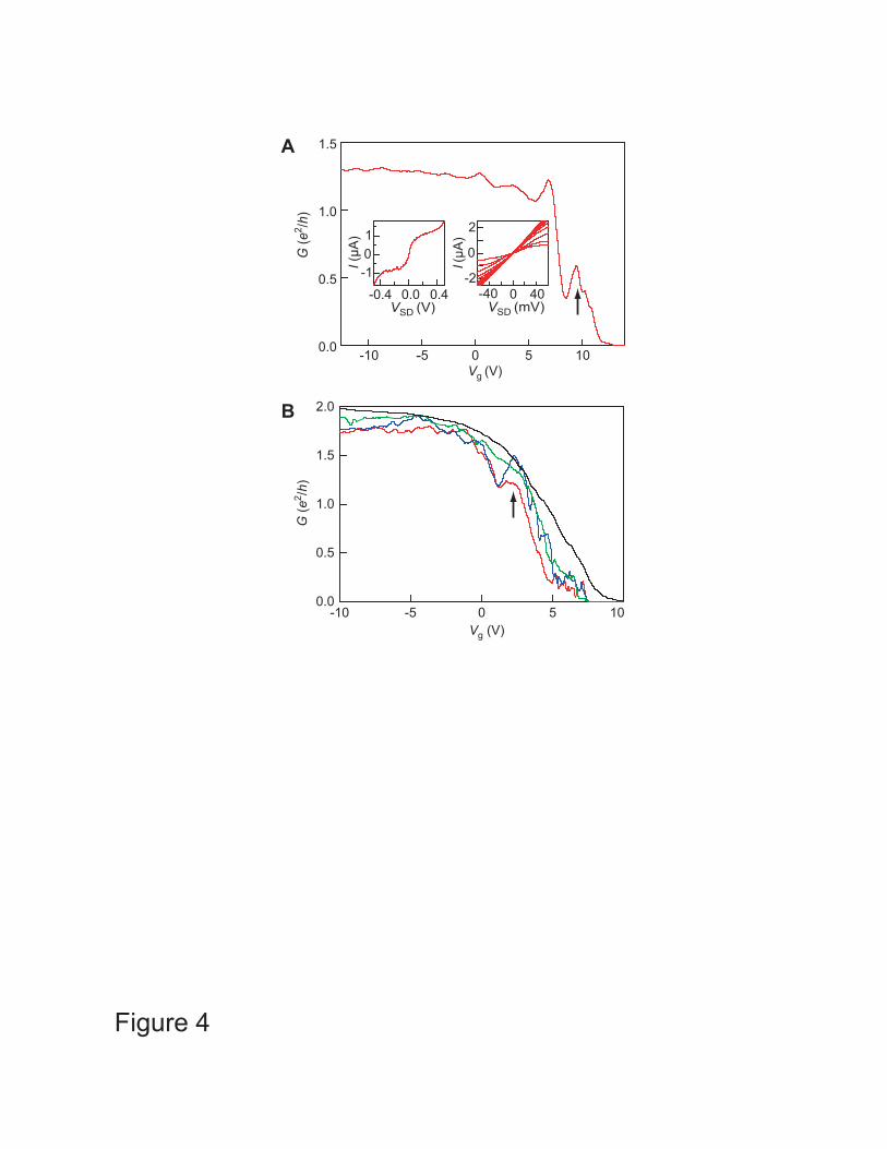
reproducible transparent contacts to the hole gas even at low temperatures. I-VSD data obtained at
4.7 K on an annealed device with a 10 nm core (Fig. 4A, inset) close to depletion (Vg = 10 V) are
linear around VSD = 0, and thus show that the contacts are transparent at low temperatures. We
emphasize that the depletion mode p-FET behavior with transparent contacts at both room and
low temperatures is observed for essentially all of the Ge/Si nanowire heterostructure devices
8
prepared in this way. The reproducibility of this unique contact behavior demonstrates clearly
the impact possible through band structure control.
At small bias the I-VSD curves collapse for Vg < 7 V (right inset, Fig. 4A). This behavior
is highlighted by plotting G vs. Vg (Fig. 4A), where G first rises sharply and then plateaus for Vg
< 7 V. The plateau conductance, ~50 µS, is 0.65 of 2e2/h, the value expected for a spin-
degenerate single-mode ballistic conductor (13). Variations in the plateau conductance are
suggestive of Fabry-Perot interferences (8), but are not quantified here due to their small
amplitude. Studies of additional devices show very similar results and highlight the reproducible
transport properties of the Ge/Si nanowire system. For example, Fig. 4B shows G vs. Vg recorded
at different temperatures for another 10 nm core diameter device. At 4.7 K, the device shows a
conductance plateau close to 2e2/h, which is consistent with data in Fig. 4A and the value for a
single-mode ballistic conductor. Notably, increasing temperature up to 300 K yields little change
in the value of the conductance plateau, although the slope becomes somewhat smeared. This
fact implies that even at room temperature only a single 1D subband participates in transport and
that the mean free path exceeds the channel length of 170 nm; that is, transport through the Ge/Si
nanowire remains ballistic up to at least this length scale.
These results contrast data from planar 2DHG devices, where the mobility decreases
dramatically with increasing temperature due to scattering with acoustic phonons (23). In a 1D
system, acoustic phonon scattering should be suppressed due to the reduced phase space for
back-scattering (24). In the Ge/Si nanowires, we use Fermi’s golden rule to estimate the acoustic
phonon scattering rate as
)(1F2
s
2B
ap
EDvTk
ρπ
τ h
Ξ= , (1)

9
where Ξ is the deformation potential, ρ is the mass density, and sv is the velocity of sound. We
calculate the density of states 2
* 12)(rE
mEDππh
= for the first subband using the effective mass
for heavy holes, m* = 0.28me (12,18), where me is the free electron mass. We obtain
12ap 109.4~ −×τ s at room temperature for a 10 nm core diameter nanowire at EF = 10 meV
using an average sound velocity of 5400 m/s and deformation potential of 3.81 eV for Ge (12,25).
The mean free path calculated using this value of τap and the Fermi velocity,
5*FF 101.1~/2 ×= mEv m/s, is 540 nm. This estimate is consistent with our experimental
results, and moreover, suggests that room-temperature ballistic transport in Ge/Si nanowires is
possible on a 0.5 µm scale assuming other scattering processes are suppressed. Room
temperature ballistic transport has been reported previously in metallic and semiconducting
carbon nanotubes (9,26), and was attributed to the topological singularity at k = 0 due to its
unique band structure in metallic nanotubes (27,28). Reduced acoustic phonon scattering in 1D
explains room temperature ballistic transport in Ge/Si nanowires, although a more detailed
theoretical analysis, including the confinement effects of phonon modes, will be needed to
quantify the limits of this interesting behavior.
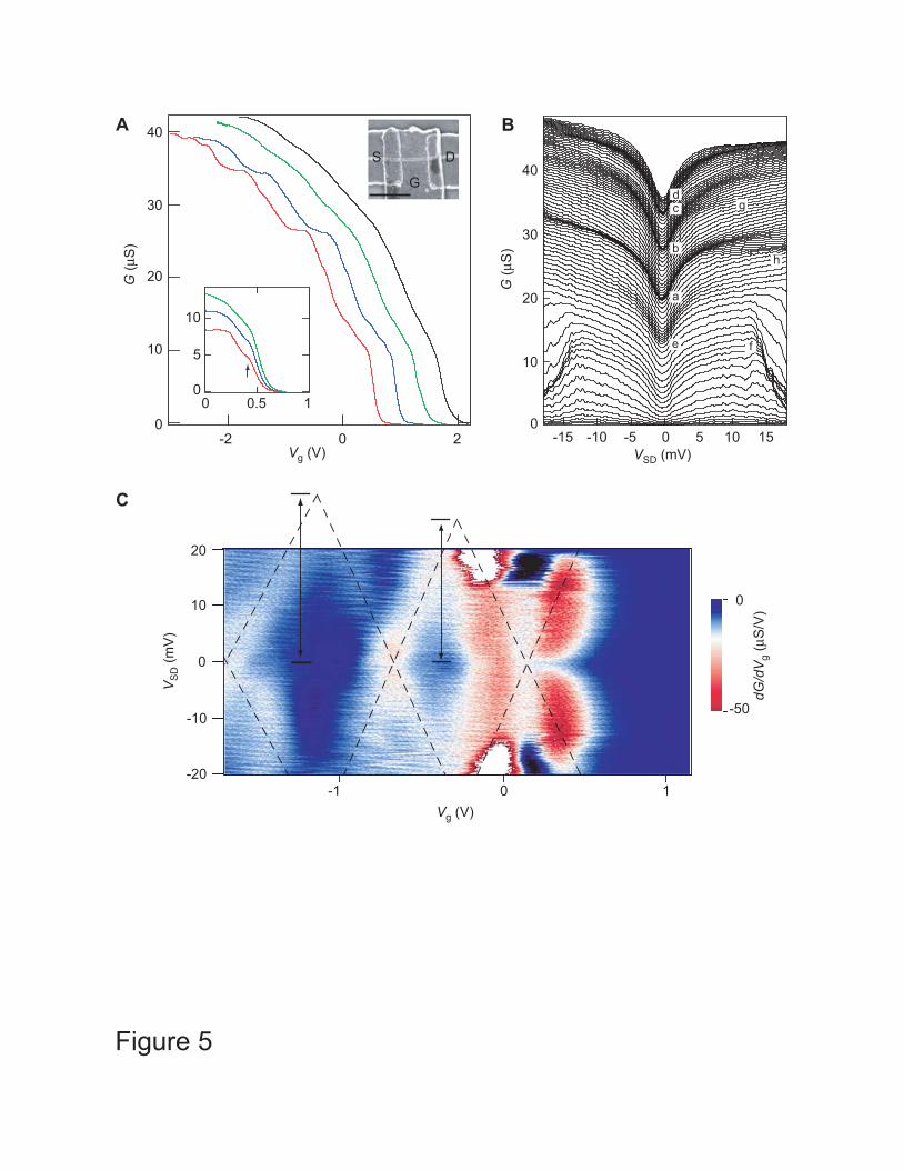
In addition, we have studied devices with a top-gate structure, which increases the gate
coupling, in order to probe transport through more than one subband. G-Vg data recorded on a
400 nm long device (Fig. 5A) shows four distinct conductance plateaus at 5 K. We attribute
these plateaus to transport through the first four subbands in the Ge/Si nanowire, and confirm
this assignment by plotting G–VSD for different values of Vg (Fig. 5B). In this plot, the
conductance plateaus appear as dark regions, labeled as a-d, where several G-VSD curves at
different Vg overlap, since Vg does not affect G in the plateau regions. At large VSD these integer

10
plateaus evolve into “half” plateaus (f-g) when the source and drain chemical potentials cross
different subbands (29,30). For example, the 0.5 plateau, appearing as the dark region labeled f,
corresponds to the case where the source potential drops below the first subband bottom while
the drain potential still lies above it (29). Similarly, feature g corresponds to the 1.5 plateau,
which evolves from the second (b) and first (a) subbands. The small cusp feature near zero-bias
in the G-VSD data is due to shallow potential barriers (31) with heights of a few meV. The
potential barriers are likely caused by non-optimal fabrication process in these top-gated devices,
since they are absent in the bottom gated devices studied earlier. The existence of shallow
barriers also explains the thermal activation behavior observed in G measured at zero-bias (but
not in G measured outside the cusp at 8 mV), and values of the conductance on the plateaus less
than multiples of 2e2/h.
The assignment of these features to 1D subbands in the Ge/Si nanowires was further
analyzed by quantifying the level spacings. Such features appear more pronounced after
numerically differentiate G against Vg (29,30). A plot of the transconductance, dG/dVg, as a
function of VSD and Vg (Fig. 5C) shows zero or low values at conductance plateaus and high
values in the transition regions between plateaus, which are highlighted by dashed lines in Fig.
5C. The subband spacings are obtained directly from these data as the VSD values at the apexes of
the full plateaus (i.e., the extrapolated intersections of the dashed lines), which yield ∆E1,2 = 25
mV and ∆E2,3 = 30 mV. For comparison, we have calculated the subband spacings using an
effective mass model with a cylindrical confinement potential with radius r to approximate the
Ge/Si nanowire structure. The energy levels of the 1D modes due to radial confinement are
2*
22
2 rmu
E nih= , (2)

11
where niu is Bessel function )(xJ n ’s ith zero point, and m* is the hole effective mass as discussed
above. For a nanowire with 14 nm Ge core diameter, we obtain ∆E1,2 = 25 mV and ∆E2,3 = 32
mV. These values are in good agreement with our experimental data (Fig. 5C), and thus provide
strong support for our assignment of discrete 1D subbands in the Ge/Si nanowire
heterostructures.
Lastly, a reproducible feature is observed with a conductance value ca. 0.7 times the first
plateau in the bottom-gated (Fig. 4, vertical arrows) and top-gated (Fig. 5A, inset; Fig. 5B, label-
e) devices. Similar features, termed “0.7 structure”, have been observed previously on quantum
point contacts and quantum wires formed in clean 2DEG samples (29,32,33). This feature is
generally believed to be caused by spontaneous spin polarization in low-dimensional interacting
electron gas systems (32) due to the formation of a spin gap (33) or a localized spin (29).
Temperature dependent data recorded on a back-gated Ge/Si device (Fig. 4B) show that the 0.7
feature initially increases in magnitude and then broadens as temperature is increased to 50 K,
consistent with the spin-gap hypothesis (33). These results suggest that the “0.7 structure” is not
restricted to electron gas samples, but a universal phenomenon in 1D systems. In this regard, the
heavier effective mass of holes in the Ge/Si nanowires compared to electrons will yield a larger
interaction parameter (6,34), and should make Ge/Si nanowires interesting to study in greater
detail in the future.
In conclusion, we have used band-structure design and controlled epitaxial growth to
create a 1D hole gas system in Ge/Si core/shell nanowire heterostructures. We have observed
ballistic transport through individual 1D subbands due to confinement of carriers in the radial
direction. Significantly, the conductance shows little temperature dependence, suggesting a room
temperature carrier mean free path on the order of several hundred nanometers. We believe that
12
the long mean free path, transparent contacts, and high device yield of the Ge/Si system make it
attractive for both fundamental studies of strongly interacting low dimensional systems and
applications as very high-performance nanoelectronic and quantum devices, and more generally,
that band-structure design and controlled epitaxial growth will open many opportunities for
fundamental studies in 1D nanowires in the future.

13
References
1. McEuen, P. L., Fuhrer, M. S. & Park, H. K. (2002) IEEE Trans. Nanotechnol. 1, 78-85.
2. Lieber, C. M. (2003) MRS Bulletin 28, 486-491.
3. Samuelson, L. (2003) Mater. Today 6, 22-31.
4. Cui, Y., Lauhon, L. J., Gudiksen, M. S., Wang, J. F. & Lieber, C. M. (2001) Appl. Phys.
Lett 78, 2214-2216.
5. Wu, Y., Cui, Y., Huynh, L., Barrelet, C. J., Bell, D. C. & Lieber, C. M. (2004) Nano Lett.
4, 433-436.
6. Yacoby, A., Stormer, H. L., Wingreen, N. S., Pfeiffer, L. N., Baldwin, K. W. & West, K.
W. (1996) Phys. Rev. Lett. 77, 4612-4615.
7. Bockrath, M., Cobden, D. H., Rinzler, A. G., Smalley, R. E., Balents, L. & McEuen, P. L.
(1999) Nature 397, 598-601.
8. Liang, W. J., Bockrath, M., Bozovic, D., Hafner, J. H., Tinkham, M. & Park, H. (2001)
Nature 411, 665-669.
9. Javey, A., Guo, J., Paulsson, M., Wang, Q., Mann, D., Lundstrom, M. & Dai, H. J. (2004)
Phys. Rev. Lett. 92, 106804.
10. Biercuk, M. J., Mason, N., Martin, J., Yacoby, A. & Marcus, C. M. (2005) Phys. Rev.
Lett. 94, 026801.
11. Dingle, R., Stormer, H. L., Gossard, A. C. & Wiegmann, W. (1978) Appl. Phys. Lett. 33,
665-667.
12. Schäffler, F. (1997) Semicond. Sci. Technol. 12, 1515-1549.
13. Beenakker, C. W. J. & van Houten, H. (1991) in Solid State Physics: Advances in
Research and Applications, eds. Ehrenreich, H. & Turnbull, D. (Academic Press, San
Diego), Vol. 44, pp. 109-125.
14
14. van Wees, B. J., Vanhouten, H., Beenakker, C. W. J., Williamson, J. G., Kouwenhoven,
L. P., Vandermarel, D. & Foxon, C. T. (1988) Phys. Rev. Lett. 60, 848-850.
15. Sohn, L. L., Kouwenhoven, L. P. & Schön, G. (1997) Mesoscopic Electron Transport
(Kluwer, Dordecht).
16. Van de Walle, C. G. & Martin, R. M. (1986) Phys. Rev. B. 34, 5621-5634.
17. Lauhon, L. J., Gudiksen, M. S., Wang, C. L. & Lieber, C. M. (2002) Nature 420, 57-61.
18. Sze, S. M. (1981) Physics of Semiconductor Devices (John Wiley & Sons, New York).
19. Grabert, H. & Devoret, M. H. (1992) Single charge tunneling: Coulomb blockade
phenomena in nanostructures (Plenum, New York).
20. De Franceschi, S., van Dam, J. A., Bakkers, E. P. A. M., Feiner, L. F., Gurevich, L. &
Kouwenhoven, L. P. (2003) Appl. Phys. Lett. 83, 344-346.
21. Tilke, A., Blick, R. H., Lorenz, H. & Kotthaus, J. P. (2001) J. Appl. Phys. 89, 8159-8162.
22. Zhong, Z., Fang, Y, Lu, W, & Lieber, C. M. (2005) Nano Lett. 5, 1143-1146.
23. Xie, Y. H., Monroe, D., Fitzgerald, E. A., Silverman, P. J., Thiel, F. A. & Watson, G. P.
(1993) Appl. Phys. Lett. 63, 2263-2264.
24. Sakaki, H. (1980) Jpn. J. Appl. Phys. 19, L735-L738.
25. Hensel, J. C. & Suzuki, K. (1974) Phys. Rev. B. 9, 4219-4257.
26. Park, J. Y., Rosenblatt, S., Yaish, Y., Sazonova, V., Ustunel, H., Braig, S., Arias, T. A.,
Brouwer, P. W. & McEuen, P. L. (2004) Nano Lett. 4, 517-520.
27. McEuen, P. L., Bockrath, M., Cobden, D. H., Yoon, Y. G. & Louie, S. G. (1999) Phys.
Rev. Lett. 83, 5098-5101.
28. Ando, T. & Nakanishi, T. (1998) J. Phys. Soc. Jpn. 67, 1704-1713.
29. Cronenwett, S. M., Lynch, H. J., Goldhaber-Gordon, D., Kouwenhoven, L. P., Marcus, C.
M., Hirose, K., Wingreen, N. S. & Umansky, V. (2002) Phys. Rev. Lett. 88, 226805.
15
30. Kristensen, A., Bruus, H., Hansen, A. E., Jensen, J. B., Lindelof, P. E., Marckmann, C. J.,
Nygard, J., Sorensen, C. B., Beuscher, F., Forchel, A. et al. (2000) Phys. Rev. B. 62,
10950-10957.
31. Tilke, A., Simmel, F. C., Lorenz, H., Blick, R. H. & Kotthaus, J. P. (2003) Phys. Rev. B.
68, 075311.
32. Thomas, K. J., Nicholls, J. T., Simmons, M. Y., Pepper, M., Mace, D. R. & Ritchie, D. A.
(1996) Phys. Rev. Lett. 77, 135-138.
33. Reilly, D. J., Buehler, T. M., O'Brien, J. L., Hamilton, A. R., Dzurak, A. S., Clark, R. G.,
Kane, B. E., Pfeiffer, L. N. & West, K. W. (2002) Phys. Rev. Lett. 89, 246801.
34. Shapira, S., Sivan, U., Soloman, P. M., Buchstab, E., Tischler, M. & Yoseph, G. B. (1996)
Phys. Rev. Lett. 77, 3181-3184.
We thank C. Marcus, H. Park and D. Reilly for helpful discussions. C.M.L. acknowledges
support of this work by Intel, Defense Advanced Research Projects Agency, and the Army
Research Office.

16
Figure Captions
Figure 1. Ge/Si core/shell nanowires. Schematics of (A) a cross section through the Ge/Si
core/shell structure, and (B) the band diagram for a Si/Ge/Si heterostructure. The dashed line
indicates the position of the Fermi level, EF, which lies inside the Si band gap and below the Ge
valance band edge. (C) High resolution TEM image of a Ge/Si core/shell nanowire with 15 nm
Ge (dark gray) core diameter and 5 nm Si (light gray) shell thickness. The contrast between core
and shell is due to difference in atomic weights of Ge and Si. Scale bar is 5 nm.
Figure 2. Room temperature electrical transport in Ge/Si nanowires. (A) I-VSD characteristics
recorded on a 10 nm core diameter Ge/Si nanowire device with source drain separation L = 1 µm.
The different curves correspond to the back gate voltage Vg values of +10 V (dashed line), 0
(solid line) and -10 V (dotted line). (Lower inset) Schematic of a Ge/Si core/shell nanowire.
(Upper inset) I-Vg for the same device at VSD = -1 V. (B) I-VSD measurements on i-Si (blue, 20
nm diameter, 1 µm channel length) and i-Ge (red, 20 nm diameter, 1 µm channel length)
nanowires; the data were recorded for Vg = 0 and -10 V, corresponding to off and on states,
respectively. (Inset) Schematic of the i-Si (blue) and i-Ge (red) nanowires.
Figure 3. Coulomb blockade (CB) in unannealed Ge/Si devices. (A) I-Vg for a 10 nm core
diameter Ge/Si nanowire (T = 1.5 K, VSD = 0.5 mV, L =112 nm). The gate capacitance is
Cg=e/∆VCB= 3.2 aF, where ∆VCB is the period of the CB oscillation. Inset, I-VSD data taken at Vg
= -9.38 V showing the CB gap. (B) Coulomb diamonds in G-VSD-Vg plot for the device in A. (C)
G-VSD-Vg plot for another 10 nm core diameter nanowire with L = 385 nm, Cg = 15.8 aF for this
device. (D) Scaling of Cg with channel length L. The red line is the theoretical prediction based
on the cylinder-on-plane model discussed in the text. Black diamonds are experimental data from
CB measurements.

17
Figure 4. Ballistic transport in Ge/Si 1D hole gas devices. (A) G-Vg recorded at 4.7 K for a 10
nm core Ge/Si nanowire with L = 350 nm. (Left inset) I-VSD curve recorded at Vg = 10 V. (Right
inset) I-VSD data recorded at Vg from 10 to -10 V in 1 V steps. (B) G-Vg data recorded for another
Ge/Si nanowire device (L = 170 nm) measured at different temperatures: black, green, blue, and
red correspond to 300, 50, 10, and 4.7 K, respectively. The conductance value on the plateau
decreases slightly with decreasing temperature. This reduction is likely due to small potential
fluctuations inside the channel, although other factors such as changes in the contact resistance
or many-body effects as discussed in Ref. 6 cannot be ruled out. The vertical arrows in (A) and
(B) highlight the 0.7 structure.
Figure 5. Transport through multiple subbands in a Ge/Si nanowire device. (A) G – Vg recorded
at different temperatures for a top-gated device (VSD = 8 mV). The red, blue, green, and black
curves correspond to 5, 10, 50, and 100 K, respectively. Data was offset horizontally for clarity.
(Upper inset) SEM image of the sample showing the source (S) drain (D) and the top gate (G)
electrodes; scale bar is 500 nm. (Lower inset) Zero-bias G-Vg recorded at 5 (red), 10 (blue) and
20 (green) K; axes have the same units as the main figure. The vertical arrow highlights the “0.7
structure”. (B) G-VSD plots recorded at Vg = 0.8 to -3.5V in 50 mV steps with no offset applied (T
= 5 K). Data taken in a different thermal cycle from A. Plateaus, labeled a-g, which appear dark
due to accumulation of G – VSD traces, are discussed in the text. Feature h evolves from the first
plateau a and the 0.7 structure e. (C) Transconductance dG/dVg as a function of VSD and Vg for
data in (B). Dashed lines are guides indicating the evolution of conductance modes with VSD and
Vg. The vertical arrows highlight values of ∆E1,2 and ∆E2,3.

EF
CB
VB
Si SiGe
Quantum Well
A
C
Ge
Si B
Figure 1
B
I (µA
)
-10
-5
011050--5-10
Vg (V)
400
200
0
-200
I (n
A)
VSD (V)-1.0 -0.5 0.0 0.5 1.0
Si
Ge
A 10
5
0
-5
-10-1.0 -0.5 0.0 0.5 1.0
I (µA
)
VSD (V)
Figure 2
2.0
0.75 0.80 0.85 0.90
2.0
0.0
- 0
14
µS
-9.1-9.3-9.5
0
-7.5
7.5
0
12
µS
VS
D(m
V)
VS
D(m
V)
I (nA
)
A
-9.0-9.5-10.0
2
1
0
3200
-20
I (nA)
5-5 0VSD (mV)
Cg (
aF)
L (nm)
D
Vg (V)
20
10
05004003002001000
Figure 3
Vg (V)
Vg (V)
B
C
2.0
1.5
1.0
0.5
0.0-10 -5 0 5 10
Vg (V)
G (e
2 /h)
A
B
Vg (V)
1.5
1.0
0.5
0.0
G (e
2 /h)
1050--5-10
-2
0
2
I (µA
)
0 40-40 VSD (mV)
10-1
0.40.0-0.4
I (µA
)
VSD (V)
Figure 4
-2 0 2 -15 -10 -5 0 5 10 15
G (µ
S)
Vg (V)
S D
G
0.5 100
5
10
40
30
20
10
0
40
30
20
10
0
VSD (mV)
A B
C
a
b
c
e
d
f
h
g
Vg (V)
VS
D (m
V)
0
-50
dG/d
Vg
(µS
/V)
-1 0 1
20
10
0
-10
-20
G (µ
S)
Figure 5
Copyright © 2022 FDOKUMEN