Electrical Characterization of Germanium Nanowires Using a ...
13
nanomaterials Article Electrical Characterization of Germanium Nanowires Using a Symmetric Hall Bar Configuration: Size and Shape Dependence Ahmad Echresh 1,2,3, *, Himani Arora 1,2 , Florian Fuchs 4,5 , Zichao Li 1 , René Hübner 1 , Slawomir Prucnal 1 , Jörg Schuster 4,5 , Peter Zahn 1,2 , Manfred Helm 1,2,3 , Shengqiang Zhou 1 , Artur Erbe 1,2 , Lars Rebohle 1 and Yordan M. Georgiev 1,2,† Citation: Echresh, A.; Arora, H.; Fuchs, F.; Li, Z.; Hübner, R.; Prucnal, S.; Schuster, J.; Zahn, P.; Helm, M.; Zhou, S.; et al. Electrical Characterization of Germanium Nanowires Using a Symmetric Hall Bar Configuration: Size and Shape Dependence. Nanomaterials 2021, 11, 2917. https://doi.org/10.3390/ nano11112917 Academic Editor: Emilio Nogales Received: 22 September 2021 Accepted: 28 October 2021 Published: 30 October 2021 Publisher’s Note: MDPI stays neutral with regard to jurisdictional claims in published maps and institutional affil- iations. Copyright: © 2021 by the authors. Licensee MDPI, Basel, Switzerland. This article is an open access article distributed under the terms and conditions of the Creative Commons Attribution (CC BY) license (https:// creativecommons.org/licenses/by/ 4.0/). 1 Institute of Ion Beam Physics and Materials Research, Helmholtz-Zentrum Dresden-Rossendorf (HZDR), 01328 Dresden, Germany; [email protected] (H.A.); [email protected] (Z.L.); [email protected] (R.H.); [email protected] (S.P.); [email protected] (P.Z.); [email protected] (M.H.); [email protected] (S.Z.); [email protected] (A.E.); [email protected] (L.R.); [email protected] (Y.M.G.) 2 International Helmholtz Research School for Nanoelectronic Network, Helmholtz-Zentrum Dresden-Rossendorf (HZDR), 01328 Dresden, Germany 3 Institute of Applied Physics, Technical University of Dresden, 01062 Dresden, Germany 4 Fraunhofer Institute for Electronic Nano Systems (ENAS), 09126 Chemnitz, Germany; fl[email protected] (F.F.); [email protected] (J.S.) 5 Center for Materials, Architectures and Integration of Nanomembranes (MAIN), Chemnitz University of Technology, 09126 Chemnitz, Germany * Correspondence: [email protected] † On Leave of Absence from the Institute of Electronics at Bulgarian Academy of Sciences, 72, Tsarigradsko Chausse Blvd., 1784 Sofia, Bulgaria. Abstract: The fabrication of individual nanowire-based devices and their comprehensive electrical characterization remains a major challenge. Here, we present a symmetric Hall bar configuration for highly p-type germanium nanowires (GeNWs), fabricated by a top-down approach using electron beam lithography and inductively coupled plasma reactive ion etching. The configuration allows two equivalent measurement sets to check the homogeneity of GeNWs in terms of resistivity and the Hall coefficient. The highest Hall mobility and carrier concentration of GeNWs at 5 K were in the order of 100 cm 2 /(Vs) and 4 × 10 19 cm -3 , respectively. With a decreasing nanowire width, the resistivity increases and the carrier concentration decreases, which is attributed to carrier scattering in the region near the surface. By comparing the measured data with simulations, one can conclude the existence of a depletion region, which decreases the effective cross-section of GeNWs. Moreover, the resistivity of thin GeNWs is strongly influenced by the cross-sectional shape. Keywords: germanium nanowires; Hall bar configuration; Hall effect; electrical characterization 1. Introduction Germanium (Ge) is a material that is most compatible with silicon (Si)-based comple- mentary metal-oxide-semiconductor (CMOS) processes. It has a higher number of electrons and hole mobility compared to Si, leading to an improved device performance [1–3]. More- over, nanowires (NWs) have been considered as an attractive building block for electronic and optoelectronic applications because of their unique properties such as a low dimen- sionality, quantum confinement, surface sensitivity, and low leakage current. Hence, GeNWs are promising high-mobility nanostructures for future nanoelectronics [4–7]. De- spite constant improvement in the performance of semiconducting NW-based devices, evaluating electrical properties of single NWs still remains a challenging task because of their small size. To date, several techniques have been developed to this end. The field effect (FE) mobility measurement is the most commonly used technique, although it has some shortcomings [8–14]. The accuracy of this method depends largely on the precision Nanomaterials 2021, 11, 2917. https://doi.org/10.3390/nano11112917 https://www.mdpi.com/journal/nanomaterials
-
Upload
khangminh22 -
Category
Documents
-
view
4 -
download
0
Transcript of Electrical Characterization of Germanium Nanowires Using a ...

nanomaterials
Article
Electrical Characterization of Germanium Nanowires Usinga Symmetric Hall Bar Configuration: Size andShape Dependence
Ahmad Echresh 1,2,3,*, Himani Arora 1,2, Florian Fuchs 4,5 , Zichao Li 1, René Hübner 1 , Slawomir Prucnal 1,Jörg Schuster 4,5, Peter Zahn 1,2 , Manfred Helm 1,2,3 , Shengqiang Zhou 1 , Artur Erbe 1,2 , Lars Rebohle 1
and Yordan M. Georgiev 1,2,†
Citation: Echresh, A.; Arora, H.;
Fuchs, F.; Li, Z.; Hübner, R.; Prucnal,
S.; Schuster, J.; Zahn, P.; Helm, M.;
Zhou, S.; et al. Electrical
Characterization of Germanium
Nanowires Using a Symmetric Hall
Bar Configuration: Size and Shape
Dependence. Nanomaterials 2021, 11,
2917. https://doi.org/10.3390/
nano11112917
Academic Editor: Emilio Nogales
Received: 22 September 2021
Accepted: 28 October 2021
Published: 30 October 2021
Publisher’s Note: MDPI stays neutral
with regard to jurisdictional claims in
published maps and institutional affil-
iations.
Copyright: © 2021 by the authors.
Licensee MDPI, Basel, Switzerland.
This article is an open access article
distributed under the terms and
conditions of the Creative Commons
Attribution (CC BY) license (https://
creativecommons.org/licenses/by/
4.0/).
1 Institute of Ion Beam Physics and Materials Research, Helmholtz-Zentrum Dresden-Rossendorf (HZDR),01328 Dresden, Germany; [email protected] (H.A.); [email protected] (Z.L.); [email protected] (R.H.);[email protected] (S.P.); [email protected] (P.Z.); [email protected] (M.H.); [email protected] (S.Z.);[email protected] (A.E.); [email protected] (L.R.); [email protected] (Y.M.G.)
2 International Helmholtz Research School for Nanoelectronic Network, Helmholtz-ZentrumDresden-Rossendorf (HZDR), 01328 Dresden, Germany
3 Institute of Applied Physics, Technical University of Dresden, 01062 Dresden, Germany4 Fraunhofer Institute for Electronic Nano Systems (ENAS), 09126 Chemnitz, Germany;
[email protected] (F.F.); [email protected] (J.S.)5 Center for Materials, Architectures and Integration of Nanomembranes (MAIN),
Chemnitz University of Technology, 09126 Chemnitz, Germany* Correspondence: [email protected]† On Leave of Absence from the Institute of Electronics at Bulgarian Academy of Sciences, 72, Tsarigradsko
Chausse Blvd., 1784 Sofia, Bulgaria.
Abstract: The fabrication of individual nanowire-based devices and their comprehensive electricalcharacterization remains a major challenge. Here, we present a symmetric Hall bar configuration forhighly p-type germanium nanowires (GeNWs), fabricated by a top-down approach using electronbeam lithography and inductively coupled plasma reactive ion etching. The configuration allowstwo equivalent measurement sets to check the homogeneity of GeNWs in terms of resistivity andthe Hall coefficient. The highest Hall mobility and carrier concentration of GeNWs at 5 K were inthe order of 100 cm2/(Vs) and 4 × 1019 cm−3, respectively. With a decreasing nanowire width, theresistivity increases and the carrier concentration decreases, which is attributed to carrier scatteringin the region near the surface. By comparing the measured data with simulations, one can concludethe existence of a depletion region, which decreases the effective cross-section of GeNWs. Moreover,the resistivity of thin GeNWs is strongly influenced by the cross-sectional shape.
Keywords: germanium nanowires; Hall bar configuration; Hall effect; electrical characterization
1. Introduction
Germanium (Ge) is a material that is most compatible with silicon (Si)-based comple-mentary metal-oxide-semiconductor (CMOS) processes. It has a higher number of electronsand hole mobility compared to Si, leading to an improved device performance [1–3]. More-over, nanowires (NWs) have been considered as an attractive building block for electronicand optoelectronic applications because of their unique properties such as a low dimen-sionality, quantum confinement, surface sensitivity, and low leakage current. Hence,GeNWs are promising high-mobility nanostructures for future nanoelectronics [4–7]. De-spite constant improvement in the performance of semiconducting NW-based devices,evaluating electrical properties of single NWs still remains a challenging task because oftheir small size. To date, several techniques have been developed to this end. The fieldeffect (FE) mobility measurement is the most commonly used technique, although it hassome shortcomings [8–14]. The accuracy of this method depends largely on the precision
Nanomaterials 2021, 11, 2917. https://doi.org/10.3390/nano11112917 https://www.mdpi.com/journal/nanomaterials
Nanomaterials 2021, 11, 2917 2 of 13
of the estimated gate capacitance. Furthermore, the FE measurement characterizes only thedepleted layer of charge carriers close to the gate and estimates the carrier concentration ofNWs by assuming a radially constant mobility. Moreover, the FE measurement is carriedout without taking into account the contact resistance, leading to an overestimation of thecarrier concentration [13–15]. Recently, the Hall effect measurement, which is a standardmethod to determine transport characteristics such as carrier mobility and carrier concen-tration in planar semiconductors, has been applied for semiconducting NWs via four-probeand three-probe device geometries [16–22]. Dissimilar to the FE measurement, the Halleffect measurement provides a more precise characterization of the carrier concentration byconsidering the entire cross-section of the NW [15]. However, the fabrication of NW-basedHall devices with a sub-30 nm diameter is a challenging process and requires a precisealignment of the metal contacts. The Hall bar configuration with narrow bars allows theprecise positioning of metal contacts on the NW sidewalls and avoids the overlapping ofmetal contacts, especially for thin NWs. Furthermore, the Hall bar configuration increasesthe accuracy of the Hall effect measurement by avoiding shorting out the Hall voltage.Recently, the Hall bar configuration has been used for silicon nanowires with a five-contactgeometry [23] and for two-dimensional (2D) materials with an eight-contact geometry [24].To the best of our knowledge, a Hall bar configuration has not been developed for GeNWsso far.
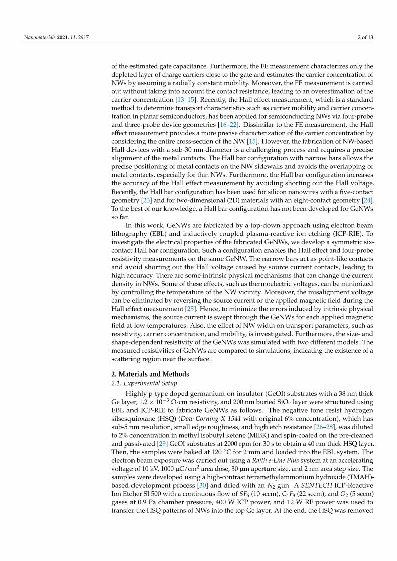
In this work, GeNWs are fabricated by a top-down approach using electron beamlithography (EBL) and inductively coupled plasma-reactive ion etching (ICP-RIE). Toinvestigate the electrical properties of the fabricated GeNWs, we develop a symmetric six-contact Hall bar configuration. Such a configuration enables the Hall effect and four-proberesistivity measurements on the same GeNW. The narrow bars act as point-like contactsand avoid shorting out the Hall voltage caused by source current contacts, leading tohigh accuracy. There are some intrinsic physical mechanisms that can change the currentdensity in NWs. Some of these effects, such as thermoelectric voltages, can be minimizedby controlling the temperature of the NW vicinity. Moreover, the misalignment voltagecan be eliminated by reversing the source current or the applied magnetic field during theHall effect measurement [25]. Hence, to minimize the errors induced by intrinsic physicalmechanisms, the source current is swept through the GeNWs for each applied magneticfield at low temperatures. Also, the effect of NW width on transport parameters, such asresistivity, carrier concentration, and mobility, is investigated. Furthermore, the size- andshape-dependent resistivity of the GeNWs was simulated with two different models. Themeasured resistivities of GeNWs are compared to simulations, indicating the existence of ascattering region near the surface.
2. Materials and Methods2.1. Experimental Setup
Highly p-type doped germanium-on-insulator (GeOI) substrates with a 38 nm thickGe layer, 1.2 × 10⁻³ Ω·cm resistivity, and 200 nm buried SiO2 layer were structured usingEBL and ICP-RIE to fabricate GeNWs as follows. The negative tone resist hydrogensilsesquioxane (HSQ) (Dow Corning X-1541 with original 6% concentration), which hassub-5 nm resolution, small edge roughness, and high etch resistance [26–28], was dilutedto 2% concentration in methyl isobutyl ketone (MIBK) and spin-coated on the pre-cleanedand passivated [29] GeOI substrates at 2000 rpm for 30 s to obtain a 40 nm thick HSQ layer.Then, the samples were baked at 120 C for 2 min and loaded into the EBL system. Theelectron beam exposure was carried out using a Raith e-Line Plus system at an acceleratingvoltage of 10 kV, 1000 µC/cm2 area dose, 30 µm aperture size, and 2 nm area step size. Thesamples were developed using a high-contrast tetramethylammonium hydroxide (TMAH)-based development process [30] and dried with an N2 gun. A SENTECH ICP-ReactiveIon Etcher SI 500 with a continuous flow of SF6 (10 sccm), C4F8 (22 sccm), and O2 (5 sccm)gases at 0.9 Pa chamber pressure, 400 W ICP power, and 12 W RF power was used totransfer the HSQ patterns of NWs into the top Ge layer. At the end, the HSQ was removed
Nanomaterials 2021, 11, 2917 3 of 13
by a dip in HF (1% in H2O) solution for 50 s. In order to fabricate the Hall contacts, EBL,metal deposition, and a lift-off process were employed. A positive tone resist, polymethylmethacrylate (PMMA), was spin-coated on the samples with the patterned GeNWs at3000 rpm for 50 s and baked at 180 C for 10 min. Then, the electron beam exposure wasperformed using the following parameters: 10 kV accelerating voltage, 120 µC/cm2 areadose, 20 µm aperture size, and 20 nm area step size. The exposed samples were developedin isopropanol/deionized water (7:3) solution. Right before nickel (Ni) deposition for themetal contacts, samples were placed into an acetic acid/DI water (1:7) solution to removethe native oxide [29]. An ultrahigh vacuum electron beam BESTEC evaporation tool wasused to deposit a 50 nm thick layer of Ni. Afterwards, the lift-off was carried out in acetone.A schematic diagram of the fabricated device with the six-contact Hall bar configuration isshown in Figure 1.
SiO2
Si
Ni contactsGe nanowire
Figure 1. Schematic diagram of the fabricated device with the six-contact Hall bar configuration.
Bright-field (BF) and high-resolution transmission electron microscopy (HR-TEM)imaging was performed with an image Cs-corrected Titan 80–300 microscope (FEI, Eind-hoven, Netherlands) operated at an accelerating voltage of 300 kV. Prior to TEM analysis,the specimen mounted in a double-tilt low-background holder was placed for 8 s into aModel 1020 Plasma Cleaner (Fischione, Export, PA, USA) to remove possible contamination.The preparation of the TEM specimen containing the cross-section of the GeNW was con-ducted by in situ lift-out using a Helios 5 CX focused ion beam (FIB) system (Thermo Fisher,Waltham, MA, USA). To protect the GeNW surface, a carbon cap layer was deposited atthe beginning with electron-beam-assisted and, subsequently, followed by Ga-FIB-assistedprecursor decomposition. Afterward, the TEM lamella was prepared using a 30 keV GaFIB with adapted currents. Its transfer to a 3-post copper lift-out grid (Omniprobe) wasperformed with an EasyLift EX nanomanipulator (Thermo Fisher). To minimize sidewalldamage, Ga ions with 5 keV energy were used for the final thinning of the TEM lamella forelectron transparency. Phonon scattering spectra of the GeOI substrate and the GeNWswere obtained by micro-Raman spectroscopy in backscattering geometry in the rangeof 100 to 600 cm−1 using a green (532 nm) Nd:YAG laser with a liquid nitrogen-cooledcharge-coupled device camera. The electrical characterization of the highly p-type dopedGeOI substrate was carried out by means of a commercial Lakeshore Hall measurementsystem with van der Pauw configuration [31]. A parameter analyzer (Agilent, 4155C) anda superconducting magnet with fields up to ±2 T were used to characterize the electricalproperties of the GeNWs with Hall bar configuration.
2.2. Modelling
The resistivity of NWs with simple shapes can be calculated analytically in case ofthin films [32], circular NWs [33], and rectangular NWs [34]. Since the fabricated GeNWsshowed a more complicated shape, shown in Figure 2c, we used the semi-numericalmodel developed by Moraga et al. [34], which can be applied to arbitrary cross-sectionalshapes. This model calculates the NW resistivity from a number of classical trajectories.The average over the classical trajectories gives the characteristic function
⟨e−di / λbulk
⟩i,
Nanomaterials 2021, 11, 2917 4 of 13
where λbulk is the mean free path of the bulk material and di is the flight distance of thei-th particle, which was calculated as follows. Starting at a given position (x,y) insidethe NW and a given direction of the charge carrier (φ,θ), the next intersection point withthe surface was calculated. The reflectivity parameter p determined the probability ofspecular reflection. In case of specular reflection, the normal component of the directionwas reversed and the next intersection point was calculated. With probability of 1-p, adiffusive scattering event occurred and the trajectory ended. A sufficiently large ensembleof trajectories was considered to obtain converged results. p = 0 corresponds to maximalsurface roughness. The inverse of the resistivity (i.e., the conductivity) in units of the bulkresistivity followed by integrating numerically over the NW cross-section and over allpossible trajectory directions as [34,35]:(
ρNWρbulk
)−1= 1 − 3
4πA
∫A
dA∫ 2π
0dφ
∫ π
0dθ cos2 θ sin θ
⟨e−di / λbulk
⟩i, (1)
where λbulk is the bulk resistivity, ρNW is the NW resistivity, A is the cross-section of theNW, φ and θ are the azimuthal and polar angles, respectively. The polar axis was along theNW axis.
3. Results and Discussion3.1. Structural Characterization
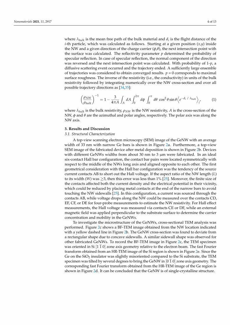
A top-view scanning electron microscopy (SEM) image of the GeNW with an averagewidth of 33 nm with narrow Ge bars is shown in Figure 2a. Furthermore, a top-viewSEM image of the fabricated device after metal deposition is shown in Figure 2b. Deviceswith different GeNWs widths from about 30 nm to 3 µm were fabricated. In an idealsix-contact Hall bar configuration, the contact bar pairs were located symmetrically withrespect to the middle of the NWs long axis and aligned opposite to each other. The firstgeometrical consideration with the Hall bar configuration was the tendency of the sourcecurrent contacts AB to short out the Hall voltage. If the aspect ratio of the NW length (L)to its width (W) was ≥3, then this error was less than 1% [25]. Moreover, the finite size ofthe contacts affected both the current density and the electrical potential in their vicinity,which could be reduced by placing metal contacts at the end of the narrow bars to avoidtouching the NW sidewalls [25]. In this configuration, a current was sourced through thecontacts AB, while voltage drops along the NW could be measured over the contacts CD,EF, CF, or DE for four-probe measurements to estimate the NW resistivity. For Hall effectmeasurements, the Hall voltage was measured via contacts CE or DF, while an externalmagnetic field was applied perpendicular to the substrate surface to determine the carrierconcentration and mobility in the GeNWs.
To investigate the microstructure of the GeNWs, cross-sectional TEM analysis wasperformed. Figure 2c shows a BF-TEM image obtained from the NW location indicatedwith a yellow dashed line in Figure 2b. The GeNW cross-section was found to deviate froma rectangular shape due to concave sidewalls. A similar sidewall shape was observed forother fabricated GeNWs. To record the BF-TEM image in Figure 2c, the TEM specimenwas oriented in Si [1 1 0] zone axis geometry relative to the electron beam. The fast Fouriertransform obtained from an HR-TEM image of the Si region is shown in Figure 2e. Since theGe on the SiO2 insulator was slightly misoriented compared to the Si substrate, the TEMspecimen was tilted by several degrees to bring the GeNW in [0 1 0] zone axis geometry. Thecorresponding fast Fourier transform obtained from the HR-TEM image of the Ge region isshown in Figure 2d. It can be concluded that the GeNW is of single-crystalline structure.
Nanomaterials 2021, 11, 2917 5 of 13
(d)
(e)
(c)
(b)
A B
C D
E F
(a)
GeNW
Bars Bars
Figure 2. (a) Top-view SEM image of a 33 nm wide GeNW with narrow Ge bars; (b) top-view SEMimage of the fabricated device with the six-contact Hall bar configuration after metal deposition. Thecontacts are labeled with A–F. (c) Cross-sectional BF-TEM image obtained from the NW location indi-cated in panel (b) by a yellow dashed line, the red dashed curve shows the cross-section consideredfor the simulation. (d,e) Fast Fourier transforms of HR-TEM images (not shown) from the Ge and Siregion marked with a white dotted and solid square in panel (c), respectively. While the BF-TEMimage and the Si HR-TEM image were obtained in Si [1 1 0] zone axis geometry (the correspondingdiffractogram is indexed in panel (e)), the Ge HR-TEM image was recorded in Ge [0 1 0] zone axisgeometry (the corresponding diffractogram is indexed in panel (d)).
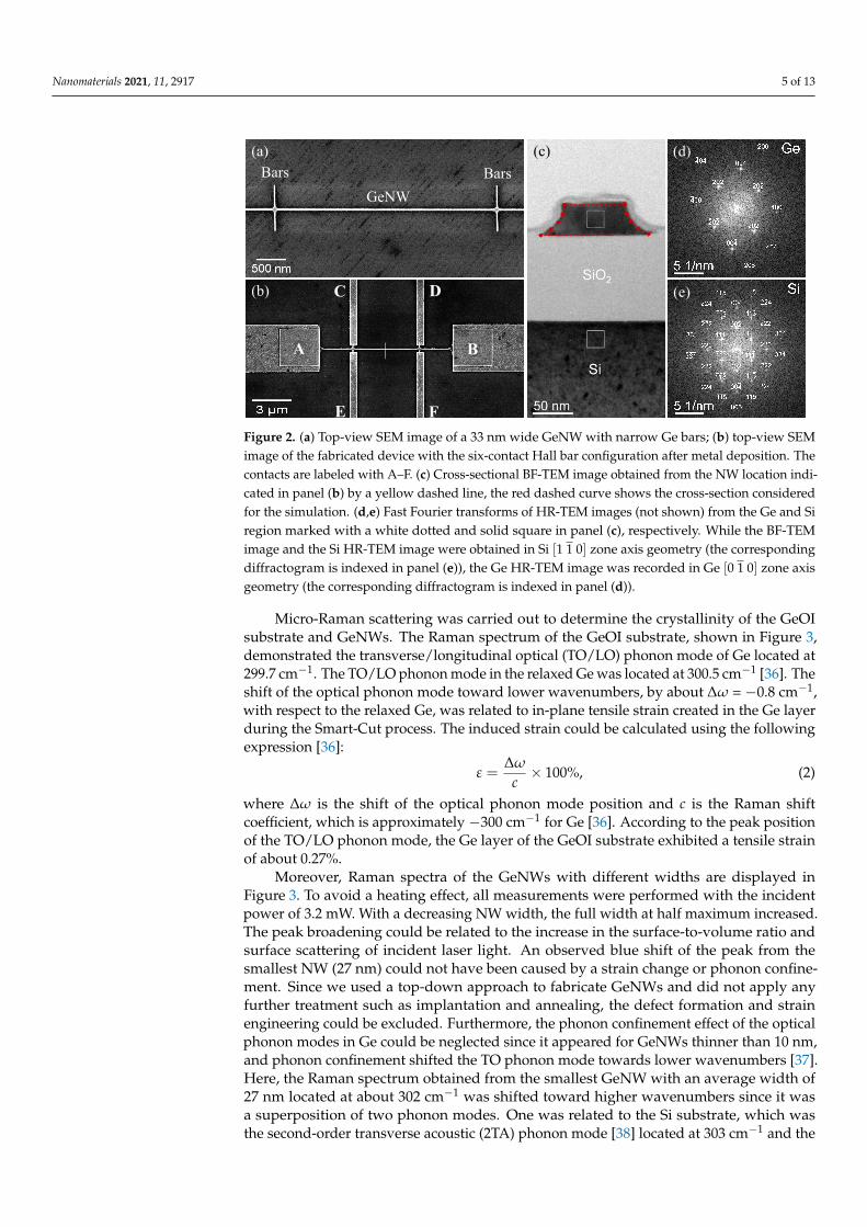
Micro-Raman scattering was carried out to determine the crystallinity of the GeOIsubstrate and GeNWs. The Raman spectrum of the GeOI substrate, shown in Figure 3,demonstrated the transverse/longitudinal optical (TO/LO) phonon mode of Ge located at299.7 cm−1. The TO/LO phonon mode in the relaxed Ge was located at 300.5 cm−1 [36]. Theshift of the optical phonon mode toward lower wavenumbers, by about ∆ω = −0.8 cm−1,with respect to the relaxed Ge, was related to in-plane tensile strain created in the Ge layerduring the Smart-Cut process. The induced strain could be calculated using the followingexpression [36]:
ε =∆ω
c× 100%, (2)
where ∆ω is the shift of the optical phonon mode position and c is the Raman shiftcoefficient, which is approximately −300 cm−1 for Ge [36]. According to the peak positionof the TO/LO phonon mode, the Ge layer of the GeOI substrate exhibited a tensile strainof about 0.27%.
Moreover, Raman spectra of the GeNWs with different widths are displayed inFigure 3. To avoid a heating effect, all measurements were performed with the incidentpower of 3.2 mW. With a decreasing NW width, the full width at half maximum increased.The peak broadening could be related to the increase in the surface-to-volume ratio andsurface scattering of incident laser light. An observed blue shift of the peak from thesmallest NW (27 nm) could not have been caused by a strain change or phonon confine-ment. Since we used a top-down approach to fabricate GeNWs and did not apply anyfurther treatment such as implantation and annealing, the defect formation and strainengineering could be excluded. Furthermore, the phonon confinement effect of the opticalphonon modes in Ge could be neglected since it appeared for GeNWs thinner than 10 nm,and phonon confinement shifted the TO phonon mode towards lower wavenumbers [37].Here, the Raman spectrum obtained from the smallest GeNW with an average width of27 nm located at about 302 cm−1 was shifted toward higher wavenumbers since it wasa superposition of two phonon modes. One was related to the Si substrate, which wasthe second-order transverse acoustic (2TA) phonon mode [38] located at 303 cm−1 and the
Nanomaterials 2021, 11, 2917 6 of 13
second one, much weaker, located at about 300 cm−1 was the TO phonon mode of 27 nmwidth GeNW.
2 4 0 2 6 0 2 8 0 3 0 0 3 2 0 3 4 0 3 6 0
1 0 1
1 0 2
1 0 3
1 0 4
Intens
ity (ar
b. unit
)
R a m a n S h i f t ( c m - 1 )
G e O I s u b s t r a t e W i d t h = 3 1 2 n m W i d t h = 9 5 n m W i d t h = 4 7 n m W i d t h = 2 7 n m
Figure 3. Raman spectra of GeOI substrate and GeNWs with the incident power of 3.2 mW.
3.2. Two- and Four-Probe Measurements
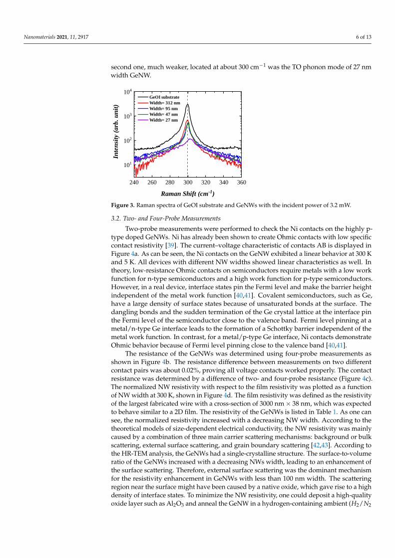
Two-probe measurements were performed to check the Ni contacts on the highly p-type doped GeNWs. Ni has already been shown to create Ohmic contacts with low specificcontact resistivity [39]. The current–voltage characteristic of contacts AB is displayed inFigure 4a. As can be seen, the Ni contacts on the GeNW exhibited a linear behavior at 300 Kand 5 K. All devices with different NW widths showed linear characteristics as well. Intheory, low-resistance Ohmic contacts on semiconductors require metals with a low workfunction for n-type semiconductors and a high work function for p-type semiconductors.However, in a real device, interface states pin the Fermi level and make the barrier heightindependent of the metal work function [40,41]. Covalent semiconductors, such as Ge,have a large density of surface states because of unsaturated bonds at the surface. Thedangling bonds and the sudden termination of the Ge crystal lattice at the interface pinthe Fermi level of the semiconductor close to the valence band. Fermi level pinning at ametal/n-type Ge interface leads to the formation of a Schottky barrier independent of themetal work function. In contrast, for a metal/p-type Ge interface, Ni contacts demonstrateOhmic behavior because of Fermi level pinning close to the valence band [40,41].
The resistance of the GeNWs was determined using four-probe measurements asshown in Figure 4b. The resistance difference between measurements on two differentcontact pairs was about 0.02%, proving all voltage contacts worked properly. The contactresistance was determined by a difference of two- and four-probe resistance (Figure 4c).The normalized NW resistivity with respect to the film resistivity was plotted as a functionof NW width at 300 K, shown in Figure 4d. The film resistivity was defined as the resistivityof the largest fabricated wire with a cross-section of 3000 nm × 38 nm, which was expectedto behave similar to a 2D film. The resistivity of the GeNWs is listed in Table 1. As one cansee, the normalized resistivity increased with a decreasing NW width. According to thetheoretical models of size-dependent electrical conductivity, the NW resistivity was mainlycaused by a combination of three main carrier scattering mechanisms: background or bulkscattering, external surface scattering, and grain boundary scattering [42,43]. According tothe HR-TEM analysis, the GeNWs had a single-crystalline structure. The surface-to-volumeratio of the GeNWs increased with a decreasing NWs width, leading to an enhancement ofthe surface scattering. Therefore, external surface scattering was the dominant mechanismfor the resistivity enhancement in GeNWs with less than 100 nm width. The scatteringregion near the surface might have been caused by a native oxide, which gave rise to a highdensity of interface states. To minimize the NW resistivity, one could deposit a high-qualityoxide layer such as Al2O3 and anneal the GeNW in a hydrogen-containing ambient (H2/N2

Nanomaterials 2021, 11, 2917 7 of 13
forming gas), which would reduce the interface states and terminate the dangling bondswith hydrogen [44,45].
(a) (b)
(c) (d)
3333
Figure 4. (a) Current–voltage curve via two-probe measurement; (b) voltage–current curve via four-probe measurement of GeNW with an average width of 33 nm. (c) Two- and four-probe resistanceand (d) normalized GeNW resistivity as a function of NW width.
Table 1. Resistivity (ρ), carrier concentration (n), carrier mobility (µH), and average relaxation timeof carriers (τp) at room temperature.
NW Width (nm) ρ (10−3 Ω·cm) n (1019 cm−3) µH (cm2V−1s−1) τp (10−15 s)
3156 1.87 4.28 78.0 9.3540 1.81 4.67 73.8 8.8312 1.99 4.94 63.3 7.595 2.24 4.32 64.4 7.733 4.29 4.05 35.9 4.3
3.3. Simulated Normalized Resistivity
To quantify the surface and sidewall scattering, the normalized resistivity of GeNWswas fitted, first, with a 1/We f f behavior, as shown in Figure 4d (Model 1). The effectiveNW width, We f f = W − 2dsc, took into account a part of the volume near the sidewallswhich did not contribute to the conductivity caused by the enhanced scattering close to thesidewalls. The thickness dsc was determined to be about 6.5 nm.
In addition, the normalized resistivity was calculated using model two, similar toMoraga et al. [34], which was developed for metallic NWs. This model is based on theBoltzmann transport equation as described in Section 2.2. The cross-section was modeledas shown in Figure 2c. The points along the sidewalls followed a Bezier curve. Thearea of the resulting polygon was used to calculate the experimental resistivity from theresistance values.
Nanomaterials 2021, 11, 2917 8 of 13
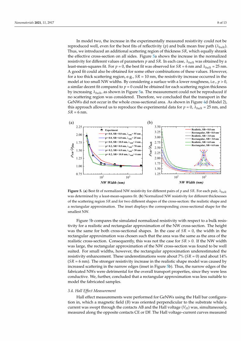
In model two, the increase in the experimentally measured resistivity could not bereproduced well, even for the best fits of reflectivity (p) and bulk mean free path (λbulk).Thus, we introduced an additional scattering region of thickness SR, which equally shrankthe effective cross-section on all sides. Figure 5a shows the increase in the normalizedresistivity for different values of parameters p and SR. In each case, λbulk was obtained by aleast-mean-squares fit. For p = 0, the best fit was observed for SR = 6 nm and λbulk = 25 nm.A good fit could also be obtained for some other combinations of these values. However,for a too thick scattering region, e.g., SR = 10 nm, the resistivity increase occurred in themodel at too small NW widths. By considering a surface with a lower roughness, i.e., p > 0,a similar decent fit compared to p = 0 could be obtained for each scattering region thicknessby increasing λbulk, as shown in Figure 5a. The measurement could not be reproduced ifno scattering region was considered. Therefore, we concluded that the transport in theGeNWs did not occur in the whole cross-sectional area. As shown in Figure 4d (Model 2),this approach allowed us to reproduce the experimental data for p = 0, λbulk = 25 nm, andSR = 6 nm.
(a) (b)
Figure 5. (a) Best fit of normalized NW resistivity for different pairs of p and SR. For each pair, λbulkwas determined by a least-mean-squares fit. (b) Normalized NW resistivity for different thicknessesof the scattering region SR and for two different shapes of the cross-section: the realistic shape anda rectangular approximation. The inset displays the corresponding cross-sectional shape for thesmallest NW.
Figure 5b compares the simulated normalized resistivity with respect to a bulk resis-tivity for a realistic and rectangular approximation of the NW cross-section. The heightwas the same for both cross-sectional shapes. In the case of SR = 0, the width in therectangular approximation was chosen such that the area was the same as the area of therealistic cross-section. Consequently, this was not the case for SR > 0. If the NW widthwas large, the rectangular approximation of the NW cross-section was found to be wellsuited. For small widths, however, the rectangular approximation underestimated theresistivity enhancement. These underestimations were about 7% (SR = 0) and about 14%(SR = 6 nm). The stronger resistivity increase in the realistic shape model was caused byincreased scattering in the narrow edges (inset in Figure 5b). Thus, the narrow edges of thefabricated NWs were detrimental for the overall transport properties, since they were lessconductive. We, further, concluded that a rectangular approximation was less suitable tomodel the fabricated samples.
3.4. Hall Effect Measurement
Hall effect measurements were performed for GeNWs using the Hall bar configura-tion in, which a magnetic field (B) was oriented perpendicular to the substrate while acurrent was swept through the contacts AB and the Hall voltage (VH) was, simultaneously,measured along the opposite contacts CE or DF. The Hall voltage–current curves measured

Nanomaterials 2021, 11, 2917 9 of 13
at different applied magnetic fields in the range of −1.4 T to +1.4 T are shown in Figure 6a.The Hall voltage was given by [46]:
VH =1
nq× IB
t, (3)
where n is the carrier concentration, q is the elementary charge, and t is the height of theGeNWs. The Hall resistance, obtained using the slope of the Hall voltage–current curve,as a function of an applied magnetic field, is presented in Figure 6b. Using the slope ofHall resistance vs. magnetic field and Equation (3), the carrier concentration (n) of theGeNWs could be estimated. The carrier Hall mobility (µH) of GeNWs could be determinedby obtaining the carrier concentration and resistivity (ρ), using the following Equation [46]:
µH =1
nρq. (4)
-4x10⁻⁵ 0 4x10⁻⁵ 8x10⁻⁵-5x10⁻⁴
-4x10⁻⁴
-3x10⁻⁴
-2x10⁻⁴
-1x10⁻⁴
0
1x10⁻⁴
Hal
l V
olta
ge (
V)
Current (A)
B = -1.4 TB = -1.2 TB = -1.0 TB = -0.8 TB = -0.6 TB = -0.4 TB = -0.2 TB = 0.0 TB = 0.2 TB = 0.4 TB = 0.6 TB = 0.8 TB = 1.0 TB = 1.2 TB = 1.4 T
Width= 512 nm, T= 50 K Width= 512 nm
-1.5 -1.0 -0.5 0.0 0.5 1.0 1.5-8
-6
-4
-2
0
2
4
Hal
l Res
ista
nce
(Ω)
Magnetic Field (T)
T= 50 K
n= 4.28×1019cm-3
Linearfit
(a) (b)
Figure 6. (a) Hall voltage–current curves at different magnetics fields; (b) Hall resistance as a functionof magnetic field for GeNW with an average width of 512 nm.
The estimated carrier concentration and Hall mobility of GeNWs at room temperatureare summarized in Table 1. One can see that the smaller GeNWs had lower carrier concen-trations. This was because of the tendency of carriers to diffuse to the surface of the GeNWsand become trapped at the interface states. In general, the unpassivated GeNW is coveredby a native oxide layer (GeOx), and the interface states of the GeNW/GeOx interface act ascarrier traps, which lead to a depleted region close to the NW surface. Hence, the carrierconcentration of smaller GeNWs may be reduced. Moreover, the dielectric mismatchbetween the GeNW and the surrounding native oxide increases the ionization energy and,consequently, reduces the activation of the dopants [47–49].
3.5. Temperature-Dependent Measurement
The temperature-dependent resistivity of the GeOI substrate and GeNWs was mea-sured using van der Pauw geometry and Hall bar configuration, respectively. As seen inFigure 7a, the resistivity of the GeOI substrate and GeNWs decreased with a decreasing tem-perature, which indicated a metallic behavior. Furthermore, the temperature-dependentcarrier concentration and Hall mobility values of the GeNWs are plotted in Figure 7b,c,respectively. The carrier concentration of GeNWs decreased at low temperatures because offreezing out of the intrinsic carriers. The carrier mobility was proportional to the relaxationtime (τ) [46],
µH =qτ
m∗ , (5)
where m∗ is the hole effective mass. The thermal lattice vibrations decreased at lowtemperatures, which led to longer carrier relaxation times. Moreover, the lower carrier

Nanomaterials 2021, 11, 2917 10 of 13
concentrations caused less electron–electron interactions. Therefore, the carrier mobility ofthe GeNWs increased at low temperatures. The GeNWs with an average width smallerthan 100 nm showed lower Hall mobility values because of a higher surface-to-volumeratio, which led to higher surface scattering and, consequently, a higher resistivity. Theobtained carrier mobility and its dependency on the GeNWs width was in good agreementwith previous reported results [50–52].
(a)
100 101 102
2x10⁻³
4x10⁻³
6x10-38x10-3
Res
isti
viy
(Ω.c
m)
Temperature (K)
Width= 95 nm
GeOI substrateWidth= 540 nmWidth= 312 nm
Width= 33 nm
0 50 100 150 200 250 30020
40
60
80
100
120
Hal
l M
obil
ity
(cm
2 /V.s
)
Temperature (K)
Width= 540 nmWidth= 312 nm
Width= 95 nm
Width= 33 nm
0 50 100 150 200 250 3003.2x1019
3.6x10¹⁹
4x10¹⁹
4.4x10¹⁹
4.8x10¹⁹
5.2x10¹⁹
Car
rier
Con
cen
trat
ion
(cm
-3)
Temperature (K)
Width= 540 nmWidth= 312 nmWidth= 95 nmWidth= 33 nm
(b)
(c)
Figure 7. Temperature-dependent (a) resistivity, (b) Hall mobility, and (c) carrier concentration ofGeNWs with different widths.
4. Conclusions
In summary, we presented a six-contact Hall bar configuration with symmetric contactbars to characterize the electrical properties of thin GeNWs. To minimize the errors causedby intrinsic physical mechanisms, the source current was swept for each magnetic field atlow temperatures.
It was shown that, by decreasing the NWs’ width, the Hall mobility decreased andthe NW resistivity increased, which was related to enhanced carrier scattering at the NWsurface. Two different models were used to simulate the experimental resistivity of theGeNWs. It appeared that the transport in the GeNWs did not occur in the whole cross-sectional area because of a scattering region near all NW surfaces, which reduced theeffective NW cross-section.
The surface passivation of GeNWs with a high-quality oxide layer is needed tominimize the interface states, which might lead to an increase in carrier mobility. Thepresented symmetric Hall bar configuration for GeNWs offered a precise way regardingthe Hall contacts fabrication and Hall effect measurements of thin semiconducting NWscompared to previous four-probe NW-based Hall devices.
Nanomaterials 2021, 11, 2917 11 of 13
Author Contributions: Conceptualization, A.E. (Ahmad Echresh) and H.A.; methodology, A.E.(Ahmad Echresh) (device fabrication, Raman spectroscopy and electrical characterization of GeNWs),H.A. (electrical characterization of GeNWs), F.F., P.Z., J.S. (simulation), R.H. (TEM) and Z.L. (electricalcharacterization of GeOI substrate); writing—original draft preparation, A.E. (Ahmad Echresh) andF.F.; writing—review and editing, A.E. (Artur Erbe), P.Z., S.Z., M.H., J.S., S.P., H.A., L.R. and Y.M.G.;supervision, L.R. and Y.M.G. All authors have read and approved this manuscript for submission.
Funding: This work was partially financed by the Initiative and Networking Fund of the GermanHelmholtz Association through the Helmholtz International Research School for NanoelectronicNetworks NANONET (VH-KO-606).
Institutional Review Board Statement: No humans or animals were involved for these studies.
Informed Consent Statement: No humans were involved for these studies.
Data Availability Statement: It is not applicable.
Acknowledgments: Authors would like to thank Ciaran Fowley for providing facilities in theHZDR clean room. Furthermore, Claudia Neisser and Tommy Schönherr are acknowledged fortheir instructions with conducting electron beam lithography and electron beam evaporation, andoperating the probe station for electrical measurements. Many thanks go to Ilona Skorupa, whohelped with performing the metal deposition for unpatterned GeOI substrates and Annette Kunzfor TEM lamella preparation. Furthermore, the use of the HZDR Ion Beam Center TEM facilities isgratefully acknowledged.
Conflicts of Interest: There are no conflict to declare.
References1. Duffy, R.; Shayesteh, M.; Thomas, K.; Pelucchi, E.; Yu, R.; Gangnaik, A.; Georgiev, Y.M.; Carolan, P.; Petkov, N.; Long, B.; et al.
Access resistance reduction in Ge nanowires and substrates based on non-destructive gas-source dopant in-diffusion. J. Mater.Chem. C 2014, 2, 9248–9257. [CrossRef]
2. Goley, P.S.; Hudait, M.K. Germanium based field-effect transistors: Challenges and opportunities. Materials 2014, 7, 2301–2339.[CrossRef] [PubMed]
3. Sgourou, E.; Panayiotatos, Y.; Vovk, R.; Kuganathan, N.; Chroneos, A. Diffusion and Dopant Activation in Germanium: Insightsfrom Recent Experimental and Theoretical Results. Appl. Sci. 2019, 9, 2454. [CrossRef]
4. Tutuc, E.; Appenzeller, J.; Reuter, M.C.; Guha, S. Realization of a Linear Germanium Nanowire p- n Junction. Nano Lett. 2006,6, 2070–2074. [CrossRef] [PubMed]
5. Sistani, M.; Staudinger, P.; Lugstein, A. Polarity Control in Ge Nanowires by Electronic Surface Doping. J. Phys. Chem. C 2020,124, 19858–19863. [CrossRef]
6. John, J.W.; Dhyani, V.; Georgiev, Y.M.; Gangnaik, A.S.; Biswas, S.; Holmes, J.D.; Das, A.K.; Ray, S.K.; Das, S. Ultrahigh NegativeInfrared Photoconductance in Highly As-Doped Germanium Nanowires Induced by Hot Electron Trapping. ACS Appl. Electron.Mater. 2020, 2, 1934–1942. [CrossRef]
7. Zhang, S.; Hemesath, E.R.; Perea, D.E.; Wijaya, E.; Lensch-Falk, J.L.; Lauhon, L.J. Relative influence of surface states and bulkimpurities on the electrical properties of Ge nanowires. Nano Lett. 2009, 9, 3268–3274. [CrossRef]
8. Cui, Y.; Duan, X.; Hu, J.; Lieber, C.M. Doping and electrical transport in silicon nanowires. J. Phys. Chem. B 2000, 104, 5213–5216.[CrossRef]
9. Garnett, E.C.; Tseng, Y.C.; Khanal, D.R.; Wu, J.; Bokor, J.; Yang, P. Dopant profiling and surface analysis of silicon nanowires usingcapacitance–voltage measurements. Nat. Nanotechnol. 2009, 4, 311–314. [CrossRef]
10. Mansfield, L.; Bertness, K.A.; Blanchard, P.T.; Harvey, T.E.; Sanders, A.W.; Sanford, N.A. GaN nanowire carrier concentrationcalculated from light and dark resistance measurements. J. Electron. Mater. 2009, 38, 495–504. [CrossRef]
11. Dufouleur, J.; Colombo, C.; Garma, T.; Ketterer, B.; Uccelli, E.; Nicotra, M.; Fontcuberta i Morral, A. P-doping mechanisms incatalyst-free gallium arsenide nanowires. Nano Lett. 2010, 10, 1734–1740. [CrossRef]
12. Galluccio, E.; Doherty, J.; Biswas, S.; Holmes, J.D.; Duffy, R. Field-Effect Transistor Figures of Merit for Vapor–Liquid–Solid-GrownGe1-xSn x (x = 0.03–0.09) Nanowire Devices. ACS Appl. Electron. Mater. 2020, 2, 1226–1234. [CrossRef]
13. Wunnicke, O. Gate capacitance of back-gated nanowire field-effect transistors. Appl. Phys. Lett. 2006, 89, 083102. [CrossRef]14. Khanal, D.; Wu, J. Gate coupling and charge distribution in nanowire field effect transistors. Nano Lett. 2007, 7, 2778–2783.
[CrossRef]15. Hultin, O.; Otnes, G.; Borgström, M.T.; Björk, M.; Samuelson, L.; Storm, K. Comparing Hall effect and field effect measurements
on the same single nanowire. Nano Lett. 2016, 16, 205–211. [CrossRef] [PubMed]16. Hultin, O.; Otnes, G.; Samuelson, L.; Storm, K. Simplifying nanowire Hall effect characterization by using a three-probe device
design. Nano Lett. 2017, 17, 1121–1126. [CrossRef]
Nanomaterials 2021, 11, 2917 12 of 13
17. Storm, K.; Halvardsson, F.; Heurlin, M.; Lindgren, D.; Gustafsson, A.; Wu, P.M.; Monemar, B.; Samuelson, L. Spatially resolvedHall effect measurement in a single semiconductor nanowire. Nature Nanotechnol. 2012, 7, 718. [CrossRef] [PubMed]
18. Blömers, C.; Grap, T.; Lepsa, M.; Moers, J.; Trellenkamp, S.; Grützmacher, D.; Lüth, H.; Schäpers, T. Hall effect measurements onInAs nanowires. Appl. Phys. Lett. 2012, 101, 152106. [CrossRef]
19. Heurlin, M.; Hultin, O.; Storm, K.; Lindgren, D.; Borgström, M.T.; Samuelson, L. Synthesis of doped InP core–shell nanowiresevaluated using hall effect measurements. Nano Lett. 2014, 14, 749–753. [CrossRef]
20. Lindgren, D.; Hultin, O.; Heurlin, M.; Storm, K.; Borgström, M.T.; Samuelson, L.; Gustafsson, A. Study of carrier concentration insingle InP nanowires by luminescence and Hall measurements. Nanotechnology 2015, 26, 045705. [CrossRef] [PubMed]
21. DeGrave, J.P.; Liang, D.; Jin, S. A general method to measure the Hall effect in nanowires: Examples of FeS2 and MnSi. Nano Lett.2013, 13, 2704–2709. [CrossRef]
22. Verma, A.; Borisov, K.; Connaughton, S.; Stamenov, P. Hall Effect Measurements in Rotating Magnetic Field on Sub-30-nm SiliconNanowires Fabricated by a Top–Down Approach. IEEE Trans. Electron Devices 2020, 67, 5201–5208. [CrossRef]
23. Chen, K.; Zhao, X.; Mesli, A.; He, Y.; Dan, Y. Dynamics of charge carriers in silicon nanowire photoconductors revealed by photoHall effect measurements. ACS Nano 2018, 12, 3436–3441. [CrossRef] [PubMed]
24. Dong, R.; Han, P.; Arora, H.; Ballabio, M.; Karakus, M.; Zhang, Z.; Shekhar, C.; Adler, P.; Petkov, P.S.; Erbe, A.; et al. High-mobilityband-like charge transport in a semiconducting two-dimensional metal–organic framework. Nat. Mater. 2018, 17, 1027–1032.[CrossRef]
25. Look, D.C. Electrical Characterization of GaAs Materials and Devices; John Wiley & Sons: Chechister, UK, 1989.26. Namatsu, H.; Yamaguchi, T.; Nagase, M.; Yamazaki, K.; Kurihara, K. Nano-patterning of a hydrogen silsesquioxane resist with
reduced linewidth fluctuations. Microelectron. Eng. 1998, 41, 331–334. [CrossRef]27. Georgiev, Y.; Henschel, W.; Fuchs, A.; Kurz, H. Surface roughness of hydrogen silsesquioxane as a negative tone electron beam
resist. Vacuum 2005, 77, 117–123. [CrossRef]28. Mirza, M.M.; Zhou, H.; Velha, P.; Li, X.; Docherty, K.E.; Samarelli, A.; Ternent, G.; Paul, D.J. Nanofabrication of high aspect ratio
(~50:1) sub-10 nm silicon nanowires using inductively coupled plasma etching. J. Vac. Sci. Technol. B Nanotechnol. Microelectron.Mater. Process. Meas. Phenom. 2012, 30, 06FF02. [CrossRef]
29. Gangnaik, A.S.; Georgiev, Y.M.; Collins, G.; Holmes, J.D. Novel germanium surface modification for sub-10 nm patterning withelectron beam lithography and hydrogen silsesquioxane resist. J. Vac. Sci. Technol. B Nanotechnol. Microelectron. Mater. Process.Meas. Phenom. 2016, 34, 041603. [CrossRef]
30. Henschel, W.; Georgiev, Y.; Kurz, H. Study of a high contrast process for hydrogen silsesquioxane as a negative tone electronbeam resist. J. Vac. Sci. Technol. B Microelectron. Nanometer Struct. Process. Meas. Phenom. 2003, 21, 2018–2025. [CrossRef]
31. van der Pauw, L.J. A method of measuring the resistivity and Hall coefficient on lamellae of arbitrary shape. Philips Tech. Rev.1958, 20, 220–224.
32. Fuchs, K. The conductivity of thin metallic films according to the electron theory of metals. Math. Proc. Camb. Philos. Soc. 1938,34, 100–108. [CrossRef]
33. Dingle, R. The electrical conductivity of thin wires. Proc. R. Soc. Lond. Ser. A Math. Phys. Sci. 1950, 201, 545–560.34. Moraga, L.; Arenas, C.; Henriquez, R.; Solis, B. The effect of surface roughness and grain-boundary scattering on the electrical
conductivity of thin metallic wires. Phys. Status Solidi 2015, 252, 219–229. [CrossRef]35. Chambers, R. The conductivity of thin wires in a magnetic field. Proc. R. Soc. Lond. Ser. A Math. Phys. Sci. 1950, 202, 378–394.36. Prucnal, S.; Berencén, Y.; Wang, M.; Grenzer, J.; Voelskow, M.; Hübner, R.; Yamamoto, Y.; Scheit, A.; Bärwolf, F.; Zviagin, V.; et al.
Strain and band-gap engineering in Ge-Sn alloys via P doping. Phys. Rev. Appl. 2018, 10, 064055. [CrossRef]37. Osswald, S.; Mochalin, V.; Havel, M.; Yushin, G.; Gogotsi, Y. Phonon confinement effects in the Raman spectrum of nanodiamond.
Phys. Rev. B 2009, 80, 075419. [CrossRef]38. Spizzirri, P.; Fang, J.H.; Rubanov, S.; Gauja, E.; Prawer, S. Nano-Raman spectroscopy of silicon surfaces. arXiv 2010,
arXiv:1002.2692.39. Gallacher, K.; Velha, P.; Paul, D.J.; MacLaren, I.; Myronov, M.; Leadley, D.R. Ohmic contacts to n-type germanium with low
specific contact resistivity. Appl. Phys. Lett. 2012, 100, 022113. [CrossRef]40. Lieten, R.; Degroote, S.; Kuijk, M.; Borghs, G. Ohmic contact formation on n-type Ge. Appl. Phys. Lett. 2008, 92, 022106. [CrossRef]41. Habanyama, A. Interface Control Processes for Ni/Ge and Pd/Ge Schottky and Ohmic Contact Fabrication: Part One. In
Advanced Material and Device Applications with Germanium; IntechOpen: London, UK, 2018; p. 47. [CrossRef]42. Li, R.; Mi, L.; Wang, J.; Mao, M.; Gu, W.; Zhu, Y. Conductivity Size Effect of Square Cross-Section Polycrystalline Nanowires.
Materials 2019, 12, 2129. [CrossRef]43. Xue, W.; Gu, W. Conductivity size effect of polycrystalline metal nanowires. AIP Adv. 2016, 6, 115001. [CrossRef]44. Seo, K.i.; Sharma, S.; Yasseri, A.A.; Stewart, D.R.; Kamins, T.I. Surface charge density of unpassivated and passivated metal-
catalyzed silicon nanowires. Electrochem. Solid State Lett. 2006, 9, G69. [CrossRef]45. Simanullang, M.; Usami, K.; Noguchi, T.; Surawijaya, A.; Kodera, T.; Kawano, Y.; Oda, S. Surface passivation of germanium
nanowires using Al2O3 and HfO2 deposited via atomic layer deposition technique. Jpn. J. Appl. Phys. 2014, 53, 06JG04. [CrossRef]46. Colinge, J.P.; Colinge, C.A. Physics of Semiconductor Devices; Kluwer Academic Publishers: New York, NY, USA, 2005.47. Ou, X.; Kanungo, P.D.; Kögler, R.; Werner, P.; Gösele, U.; Skorupa, W.; Wang, X. Three-Dimensional Carrier Profiling of Individual
Si Nanowires by Scanning Spreading Resistance Microscopy. Adv. Mater. 2010, 22, 4020–4024. [CrossRef]

Nanomaterials 2021, 11, 2917 13 of 13
48. Björk, M.T.; Schmid, H.; Knoch, J.; Riel, H.; Riess, W. Donor deactivation in silicon nanostructures. Nat. Nanotechnol. 2009,4, 103–107. [CrossRef]
49. Diarra, M.; Niquet, Y.M.; Delerue, C.; Allan, G. Ionization energy of donor and acceptor impurities in semiconductor nanowires:Importance of dielectric confinement. Phys. Rev. B 2007, 75, 045301. [CrossRef]
50. Nguyen, B.M.; Taur, Y.; Picraux, S.T.; Dayeh, S.A. Diameter-independent hole mobility in Ge/Si core/shell nanowire field effecttransistors. Nano Lett. 2014, 14, 585–591. [CrossRef] [PubMed]
51. Niquet, Y.M.; Delerue, C. Carrier mobility in strained Ge nanowires. J. Appl. Phys. 2012, 112, 084301. [CrossRef]52. Moto, K.; Yoshimine, R.; Suemasu, T.; Toko, K. Improving carrier mobility of polycrystalline Ge by Sn doping. Sci. Rep. 2018,
8, 1–7.