Characterization of Semiconductor Nanowires Using Optical Tweezers
7
rXXXX American Chemical Society A dx.doi.org/10.1021/nl200720m | Nano Lett. XXXX, XXX, 000–000 LETTER pubs.acs.org/NanoLett Characterization of Semiconductor Nanowires Using Optical Tweezers Peter J. Reece,* ,† Wen Jun Toe, † Fan Wang, † Suriati Paiman, ‡,§ Qiang Gao, ‡ H. Hoe Tan, ‡ and C. Jagadish ‡ † School of Physics, The University of New South Wales, Sydney, NSW 2052, Australia ‡ Department of Electronic Materials Engineering, Research School of Physics and Engineering, The Australian National University, Canberra, ACT 0200, Australia § Department of Physics, Faculty of Science, Universiti Putra Malaysia, 43400 Serdang, Selangor, Malaysia S emiconductor nanowires, defined by cross-sectional dimen- sions of tens to hundreds nanometers and lengths of several micrometers, are currently under investigation for a range of physical and chemical properties that are derived in part by their unique nanoscale geometry. Strong light scattering by semicon- ductor nanowires may be utilized for enhanced light trapping in photovoltaic applications, 1 nanowires combined with organic semiconductors are appropriate for bulk heterojunctions devices, and large surface to volume ratios exhibited by nanowires provide a platform for nanoscale-chemical sensing elements. 2 In terms of potential device applications, both composition and geometric factors are combined to deliver new functional devices from single nanowire elements including nanolasers, 3 photodetectors, 4 single nanowire transistors 5 and field emission sources. These elements may also be combined to create a new architecture for an integrated microprocessor. 6 Semiconductor nanowire devices may include axial or radial quantum heterostructures, 7 electrical doping and heterojunctions, as well as metallic or dielectric coating for supporting optical or plasmonic waveguiding. As the dimensions of the nanoscale objects are critical in determining functionality in associated devices, it is essential to develop effective tools with the ability to characterize individual objects, rather than rely on bulk or ensemble average measure- ments. For nanowires with well-defined geometric forms, optical tweezers offers a potentially powerful tool for investigating phy- sical and optical properties of individual objects. With optical tweezers, nanowires may be isolated and controllably manipu- lated in three-dimensions, 8 interrogated using spectroscopic tech- niques such as microphotoluminescence, 9 and assembled into predetermined arrangements over fiduciary registration points for further microprocessing. 10 Importantly, the natural Brownian dynamics of the nanowires trapped in an optical tweezers may also provide insights into nanowire properties. Physical properties such as length, width, refractive index, and extinction coefficient all influence the optical gradient and scattering forces generated by laser, which in turn affects the motion of the trapped objects driven by thermal motion. Such physical parameters may be elucidated by monitoring the thermal motion of the nanowires with respect to the center of the optical trap using interferometry techniques. Part of the difficulty associated with conducting such quanti- tative trapping measurements on irregularly shaped objects or polydispersed suspensions, such as nanowires, is that the position calibration is unique for the particular object under investigation. This is in contrast to monodispersed spherical suspensions where all particles may be assumed to have a common optical response for the position sensitive detector (PSD)—for a given optical arrangement. 11 Even for methods such as the power spectrum analysis, 12 where absolute position calibration is unnecessary, the need to determine physical dimensions to account for hydro- dynamic drag can often lead to uncertainty in absolute values of trap stiffness and associated optical force measurements. Meth- ods have been proposed to circumvent this problem for micro- particles; Greenleaf et al. 13 used a weak secondary laser source with different wavelength as a detection beam, which allows indepen- dent control of position of the trapped object with respect to the detection beam. In this scheme, optically trapped objects are scanned across a static detection beam using precise positioning of the tweezers beam (e.g., using galvanostatic mirrors) and the response of the PSD is recorded. Here we present a new method for calibration of trapped objects based on fast acousto-optic switching and position sensi- tive detection using a back focal plane interferometry. This Received: March 3, 2011 Revised: April 24, 2011 ABSTRACT: We report on the optical trapping characteristics of InP nanowires with dimensions of 30 ((6) nm in diameter and 215 μm in length. We describe a method for calibrating the absolute position of individual nanowires relative to the trapping center using synchronous high-speed position sensing and acousto-optic beam switching. Through Brownian dynamics we investigate effects of the laser power and polarization on trap stability, as well as length dependence and the effect of simulta- neous trapping multiple nanowires. KEYWORDS: Semiconductor nanowires, optical tweezers, Brownian motion, nanoparticle metrology
Transcript of Characterization of Semiconductor Nanowires Using Optical Tweezers
rXXXX American Chemical Society A dx.doi.org/10.1021/nl200720m |Nano Lett. XXXX, XXX, 000–000
LETTER
pubs.acs.org/NanoLett
Characterization of Semiconductor NanowiresUsingOptical TweezersPeter J. Reece,*,† Wen Jun Toe,† Fan Wang,† Suriati Paiman,‡,§ Qiang Gao,‡ H. Hoe Tan,‡ and C. Jagadish‡
†School of Physics, The University of New South Wales, Sydney, NSW 2052, Australia‡Department of Electronic Materials Engineering, Research School of Physics and Engineering, The Australian National University,Canberra, ACT 0200, Australia§Department of Physics, Faculty of Science, Universiti Putra Malaysia, 43400 Serdang, Selangor, Malaysia
Semiconductor nanowires, defined by cross-sectional dimen-sions of tens to hundreds nanometers and lengths of several
micrometers, are currently under investigation for a range ofphysical and chemical properties that are derived in part by theirunique nanoscale geometry. Strong light scattering by semicon-ductor nanowires may be utilized for enhanced light trapping inphotovoltaic applications,1 nanowires combined with organicsemiconductors are appropriate for bulk heterojunctions devices,and large surface to volume ratios exhibited by nanowires providea platform for nanoscale-chemical sensing elements.2 In terms ofpotential device applications, both composition and geometricfactors are combined to deliver new functional devices fromsingle nanowire elements including nanolasers,3 photodetectors,4
single nanowire transistors5 and field emission sources. Theseelements may also be combined to create a new architecture foran integrated microprocessor.6 Semiconductor nanowire devicesmay include axial or radial quantum heterostructures,7 electricaldoping and heterojunctions, as well asmetallic or dielectric coatingfor supporting optical or plasmonic waveguiding.
As the dimensions of the nanoscale objects are critical indetermining functionality in associated devices, it is essential todevelop effective tools with the ability to characterize individualobjects, rather than rely on bulk or ensemble average measure-ments. For nanowires with well-defined geometric forms, opticaltweezers offers a potentially powerful tool for investigating phy-sical and optical properties of individual objects. With opticaltweezers, nanowires may be isolated and controllably manipu-lated in three-dimensions,8 interrogated using spectroscopic tech-niques such as microphotoluminescence,9 and assembled intopredetermined arrangements over fiduciary registration pointsfor further microprocessing.10 Importantly, the natural Browniandynamics of the nanowires trapped in an optical tweezers mayalso provide insights into nanowire properties. Physical properties
such as length, width, refractive index, and extinction coefficientall influence the optical gradient and scattering forces generatedby laser, which in turn affects the motion of the trapped objectsdriven by thermal motion. Such physical parameters may beelucidated by monitoring the thermal motion of the nanowireswith respect to the center of the optical trap using interferometrytechniques.
Part of the difficulty associated with conducting such quanti-tative trapping measurements on irregularly shaped objects orpolydispersed suspensions, such as nanowires, is that the positioncalibration is unique for the particular object under investigation.This is in contrast tomonodispersed spherical suspensions whereall particles may be assumed to have a common optical responsefor the position sensitive detector (PSD)—for a given opticalarrangement.11 Even for methods such as the power spectrumanalysis,12 where absolute position calibration is unnecessary, theneed to determine physical dimensions to account for hydro-dynamic drag can often lead to uncertainty in absolute values oftrap stiffness and associated optical force measurements. Meth-ods have been proposed to circumvent this problem for micro-particles; Greenleaf et al.13 used a weak secondary laser source withdifferent wavelength as a detection beam, which allows indepen-dent control of position of the trapped object with respect to thedetection beam. In this scheme, optically trapped objects arescanned across a static detection beam using precise positioningof the tweezers beam (e.g., using galvanostatic mirrors) and theresponse of the PSD is recorded.
Here we present a new method for calibration of trappedobjects based on fast acousto-optic switching and position sensi-tive detection using a back focal plane interferometry. This
Received: March 3, 2011Revised: April 24, 2011
ABSTRACT: We report on the optical trapping characteristicsof InP nanowires with dimensions of 30 ((6) nm in diameterand 2�15 μm in length.We describe amethod for calibrating theabsolute position of individual nanowires relative to the trappingcenter using synchronous high-speed position sensing andacousto-optic beam switching. Through Brownian dynamicswe investigate effects of the laser power and polarization on trapstability, as well as length dependence and the effect of simulta-neous trapping multiple nanowires.
KEYWORDS: Semiconductor nanowires, optical tweezers, Brownian motion, nanoparticle metrology
B dx.doi.org/10.1021/nl200720m |Nano Lett. XXXX, XXX, 000–000
Nano Letters LETTER
technique allows for the calibration of the position sensitivedetector for target objects with arbitrary dimensions, while remov-ing the need for a secondary laser source. Making use of theconcepts of trap multiplexing based on time-sharing approach,14
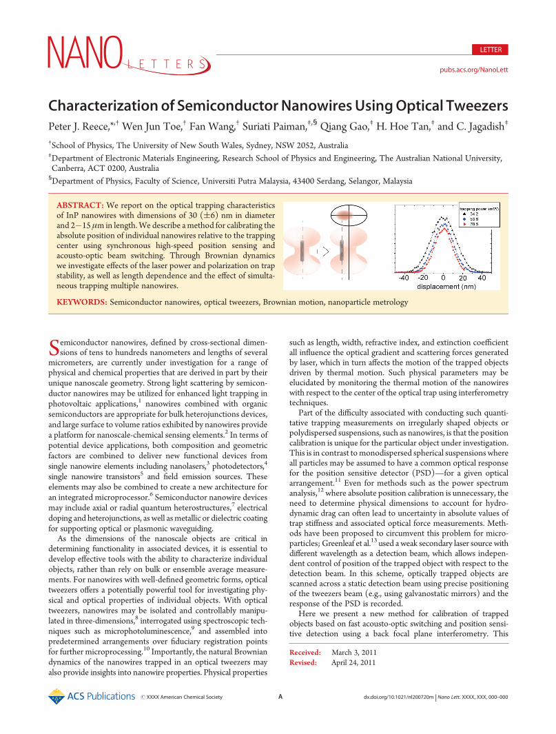
our technique uses a field programmable gate array (FPGA) dataacquisition card to synchronize the readings from the PSD withthe addressing of a two-axis acousto-opitc deflector. The calibra-tion procedure involves moving the trapped objects to differentpositions around fixed trapping center and measuring theresponse of the PSD when the beam is briefly switched back tothe origin.We apply the abovemethod to investigate the Browniandynamics of optically trapped semiconductor nanowires with verylarge aspect ratios. Specifically we investigate effects of the laserpower, laser polarization, nanowire length dependence, and theeffect of trapping multiple nanowires on trap stiffness.Experimental Methods. Figure 1a depicts the basic setup of
the optical tweezers arrangement. A linearly polarized 1064 nm
YAG laser (5 W Laser Quantum, 1064 Ventus) is used for thelaser-trapping source; a half-waveplate and polarizing beamsplitter are used to control the power at the focus. The beam isdirected through a two-axis acousto-optic deflector (AOD)(NEOSTechnologies, model 45035-3-6.5DEG-1.060XY) drivenby two digital frequency synthesizers (DFS) operating in therange of 25�45MHz. The radio frequency sources are addressedusing a FPGA data-acquisition card (National Instruments PCIe-7852R) with a 30-bit digital control word and the DFS has alatching time of 20 ns. The AOD switching rate is 4.5 μs, whichsets the system response. The deflected beam is directed towardthe back aperture of the objective through a beam-expandingtelescope to match the beam waist to the back-aperture of a 1.25numerical aperture (NA) oil immersion objective (Nikon E-plan100�). A second half waveplate is used to control the orientationof the polarization incident on the objective. An additional relaytelescope is used to ensure the AOD and back-aperture ispositioned in conjugate image planes. Scattered light fromoptically trapped objects is collected using a long workingdistance objective (S Plan Fluor ELWD 40�, 0.65 NA), whichalso acts as a condenser for bright field illumination. Theinterference pattern generated at the scattered light is relayedto a dual axis position sensitive detector (Pacific Silicon SensorsDL16-7PCBA3) with a bandwidth of 300 kHz. The signal fromthe detector is collected on the analog inputs of the FPGA dataacquisition card. Direct bright-field imaging of the nanowires wasdone using a high-frame-rate CCD camera (Basler a602f) incombination with Kohler illumination.InP nanowires used for this study were epitaxially grown on an
InP (111)B substrate bymetal organic chemical vapor deposition(MOCVD).15 The semiconductor substrates were initially im-mersed in poly-L-lysine solution and treated with gold colloidsolution containing gold nanoparticles of 30 nm in diameter. Thenanowires were then grown in the MOCVD reactor usingtrimethylindium (TMIn) and phosphine (PH3) precursors, withthe gold nanoparticles acting as seeds for the growth via thevapor�liquid�solid (VLS) mechanism.16 During growth, pres-sure was kept at 100 mbar while the temperature was set at490 �C, the V/III ratio was set at 44, and the growth time isapproximately 20 min. These growth conditions producednanowires of very uniform cylindrical geometry of dimensions30( 6 nm in diameter and up to 15 μm in length. The nanowireshad a predominantly wurtzite crystal structure, which was con-firmed by high-resolution transmission electron and scanningelectron microscopy measurements.17
For optical tweezers experiments nanowires, were suspendedin an aqueous solution by sonication of the as-grown nanowiresfrom their native substrate; the sonication process produced arange of nanowire lengths between 2 and 15 μm. A 5 μL volumeof nanowire suspension was pipetted into a sealed microfluidicchamber with a height of approximately 100 μm. To trap ananowire in the tweezers, a freely suspended nanowire wasmoved in the proximity of the laser focus—for high refractiveindex semiconductor nanowires with lengths extending beyondthe depth of focused of the optical tweezers beam, the nanowiresnaturally aligned with its long axis along the direction ofpropagation. We note that because the nanowires were regularlyshaped, we see no rotation or preferential orientation within thetrap. We also note that at trapping powers in the range ofmilliwatts to tens of milliwatts the Brownian motion is observedto be preferentially translational in nature. Time-series data ofpositional fluctuations within the trap were collected for periods
Figure 1. (a) Graphical representation of the experimental setup usedfor nanowire trapping experiments (not to scale). A 1064 nm diodepumped solid-state laser is used as the tweezers sources and a fast-switching two-axis acousto-optic deflector (AOD) is used to control theposition of the trap in the focal plane. Detection of the motion of thenanowires in the trap is achieved by back-focal plane interferometryusing a position sensitive detector (PSD). (b) PSD calibration method:the nanowire is first captured in the optical tweezers at the origin (xo);the tweezers and nanowire are displaced by a small amount; the beam istransiently switched back to the xo and the signal on the PSD isrecorded; finally, the tweezers is switched back to capture the nanowirebefore it diffuses away.

C dx.doi.org/10.1021/nl200720m |Nano Lett. XXXX, XXX, 000–000
Nano Letters LETTER
of 2 s at a rate of 10 kHz; low pass filtering was used to removeany nonthermal contributions to the nanowire motion before thedata were analyzed. After each trapping measurement thenanowire is displaced from the trap and immobilized againstthe microchamber where the length of nanowire was measured.With the aid of the illustration given in Figure 1b, the position
sensitive detector calibration procedure is outlined as follows:(i) a nanowire is trapped with its long axis aligned to thepropagation direction of the laser and the initial trapping positionis set as the trapping origin (x0, y0); (ii) the trap position is thendisplaced by a small distance (x0 þ Δx, y0) by modifying theAOD deflection angle; (iii) the laser is briefly (25 μs) switched tothe origin and the resulting scattered field recorded (via the PSD)before the beam is switched back to the displaced position;(iv) this process is repeated 2000 times to build up a statisticalaverage of the detector signal at this position. Steps ii to iv arethen repeated for a number at difference displacements aroundthe origin in the x and y direction. The detector provides voltage,Vx(diff), analogues for relative position of the interferencepattern within the active area of the detector for the x and y axisand also a sum voltage, Vx(sum), that may be used to normalizethe signal, e.g., Rx = Vx(diff)/Vx(sum). This calibration proce-dure then provides a relationship between the raw detector signalfrom the PSD and the position of the object relative to thetrapping origin.Theoretical Consideration. For small displacements, the
restoring force acting on an optically trapped object is propor-tional to its displacement from the trapping center. The strengthof the optical restoring force is largely dependent on the beamgeometry and the shape and dielectric properties of the trappedobject. For a trapped particle within an aqueous medium, thesystem can be described as a highly overdamped harmonicoscillator for the three translation coordinates.18 Using theEinstein�Ornstein�Uhlenbeck theory of Brownian motion,the motion of the trapped particle can be described by a Langevinequation in the form19
mD2xDt2
þ γ0DxDt
þ kx ¼ ð2kBTγ0Þ1=2ηðtÞ ð1Þ
where m is the mass of the particle, x(t) is the trajectory of theparticle, κ is the trap stiffness, γ 0 is the drag coefficient of theparticle, kB is Boltzmann’s constant, T is the temperature, andη(t) denotes the stochastic process of the Brownian motion ofthe trapped particle. Here the first term on the left is the inertialterm, the second is the viscous damping or Stokes drag, and thethird term is the optical restoring force. The term on right-handside denotes the Brownian forces at absolute temperature T. Asthe characteristic time for momentum relaxation through viscousdamping, tp � m/γ0 is very small (i.e., low Reynolds numberenvironment) the inertial term may be neglected. Similar equa-tions can be used to describe motion in y and z directions, butwith differing trap stiffness and drag coefficients. We note thatrotational and rocking motions have been neglected in this case;however under certain conditions elongated objects such asnanowires will exhibit such dynamics.20
To analyze the behavior of the Brownian motion, we use twostandard methods: the power spectrum and Equipartion meth-ods. Following from Berg-Sorensen and Flyvbjerg,12 the aboveequation may be approximated by
DxDt
þ 2πfcx ¼ ð2DÞ1=2ηðtÞ ð2Þ
where we have defined the corner frequency, fc � κ/2πγ0, andD = kBT/γ0 is the Einstein equation for diffusion of particlesthrough a fluid medium. By taking the Fourier transformation of(2) wemay find the power spectrum, S, is given by the Lorentzianequation
S � j~xj2T
� �¼ D=2π2
fc2 þ f 2
ð3Þ
where~x is the Fourier transform of x(t). Hence, we can obtain thevalue of fc by fitting a Lorentzian to our experimental data andthen calculate the trap stiffness κ. Note that in order to accuratelypredict the trap stiffness parameter, we need to know the form ofdrag coefficient for the objects of interest. For spherical particlessuch as colloidal microspheres this is a well-known analyticalexpression; however for more complex shapes, such as elongatedcylinders, no analytical expression is available. Here wemodel thenanowires as cylinders and compute the Stokes’ drag for cylind-rical objects based on computational models developed by TiradoandTorre.21 The drag coefficient of a cylinder with radius r, lengthl, in a fluid of viscosity η0 can be written empirically as
γc ¼4πη0l
lnð1=2rÞ þ γ^ð4Þ
where γ^ is a correction factor accounting for the ends of thenanowire, which is calculated to be 0.84.21 The nanowires used inthis study have very high aspect ratios, in the range of 70�300,and as such the log term in the denominator is only weaklydependent on the length of the wire and the drag coefficient ispredicted to be approximately linearly dependent with respect tothe length of the nanowire.The Equipartition theorem, which relates the available thermal
energy of a system to the number of degrees of freedom, may beused as an alternative approach to measure the trap stiffness foran optically trapped object.11 For a particle trapped within aharmonic potential well, the probability for the displacement of atrapped particle within a potential well is given by
PðxÞ � exp�UðxÞkBT
� �ð5Þ
where U(x) = (1/2)κx2 and x is the displacement from the trapcenter. Tracking the trapped nanowires thermal motion over aperiod of time provides a statistical histogram of particle position,which may be then used to determine the trap stiffness. Thismethod requires the absolute position of object displacementwith respect to the trap center but has an important advantage fornanowire studies in that it is independent of the drag propertiesof trapped objects, so the length of the nanowire does not need tobe known a priori in order to calculate trap stiffness values. This isimportant as the absolute lengths of specific trapped nanowiresare only resolved to the resolution of the bright field imaging.Results and Discussion. Figure 2a contains the normalized
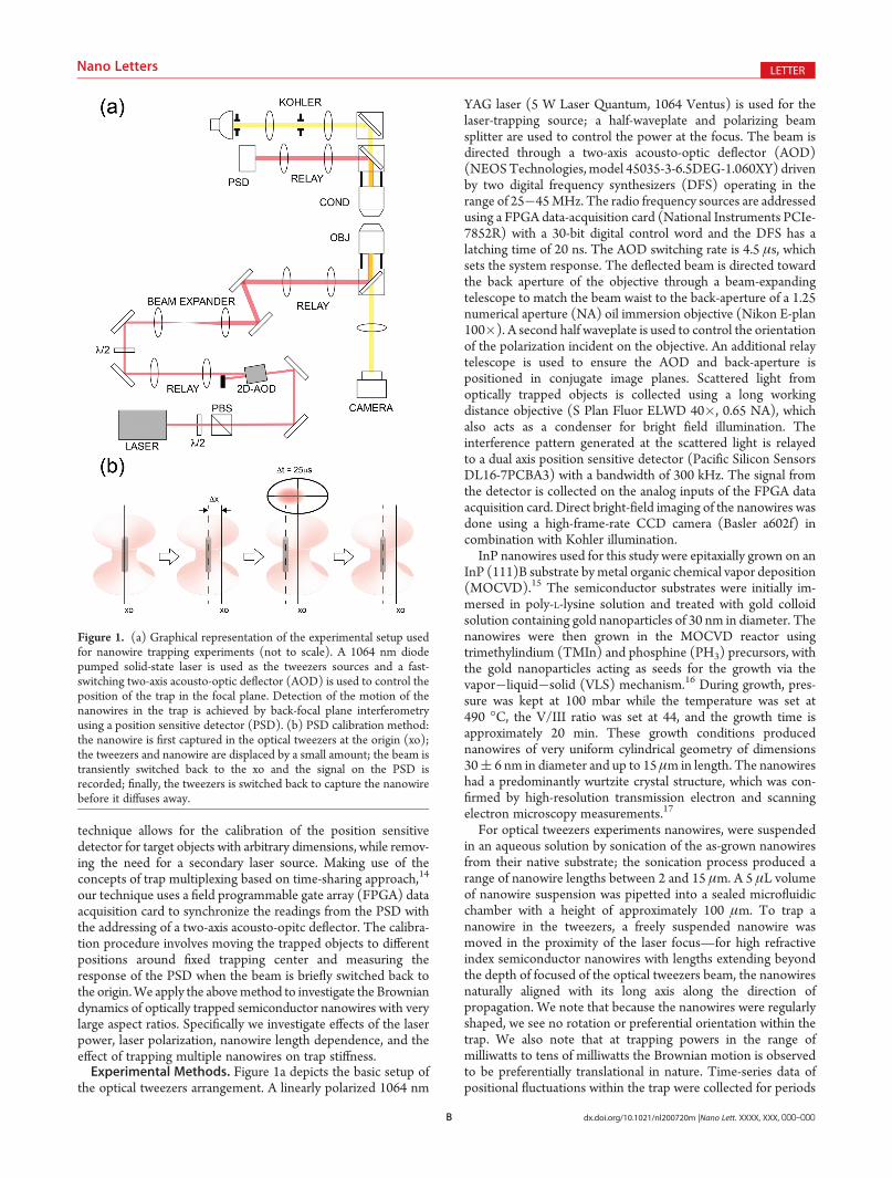
detector response of an optically trapped nanowire of length12 μm, for displacements of up to 0.6 μm from the trap center.The detector response curve exhibits a form characteristic oftrapped spherical objects22 and includes a linear region near thetrapping origin and a strongly nonlinear region at larger dis-placement; these features are consistent for all nanowire lengthstested. The graphs indicate that if the position fluctuations of thenanowire are restricted to less than approximately(200 nm thenthe linearity of the detector responsemay be preserved. Note that
D dx.doi.org/10.1021/nl200720m |Nano Lett. XXXX, XXX, 000–000
Nano Letters LETTER
the calibration is only valid for conditions where the nanowiremaintains its orientation with the long axis directed along thepropagation direction, which is the case for high refractive indexnanowires of length greatly exceeding the focal depth of thetweezers. In cases where the nanowire rotate significantly into thexy plane the asymmetry in the scattering cross-section willstrongly modify the interference pattern at the back focal plane.Figure 2b displays the linear part of the calibration curve for
nanowire of various lengths between 3 and 15 μm. An importantobservation from this graph is that the calibration curves may beresolved into discrete groups of similar values; these groupingsappear to be independent of the lengths of the nanowires. Onepossible explanation of this is that different numbers of nano-wires are simultaneously trapped in the optical tweezers. Duringthe sonication process nanowires frequently coalesce to formbound bundles of two or more nanowires. Larger bundles ofnanowires cannot be trapped as strong scattering forces from thelarge refractive index mismatch between the InP nanowire andthe surrounding fluid exceed the gradient forces for largerdiameters. From trapping experiments on single InP nanowireswhere lateral growth has been used to increase the diameter, wefind that above 150 nm the nanowires become very difficult to
trap and estimate this to be the upper limit for trapping InPnanowires in a gradient force tweezers. However, smaller group-ings of nanowires with equivalent cross sections below thiscritical dimensionmay be readily trapped and behave in amannersimilar to single nanowires. We deduce that these distinct groupsof calibration curves correspond to having different numbers ofnanowires trapped within the tweezers and that larger numbersof nanowires within the trap will result in a steeper slope of thecalibration curve.Figure 2c contains a histogram of the position fluctuation for a
10 μm nanowire at different trapping powers from 26 to 90 mWat the trapping focus; the associated trap stiffness is plotted as afunction of trapping power in Figure 2d. The general trendobserved is that increased trapping powers are associated with areduction of mean variance of the fluctuations and an increase inthe trap stiffness. At moderate trapping powers (26 mW) theposition fluctuations of 40 nm (full width half-maximum) areobserved. Increasing the power leads to an increase the localiza-tion of the nanowires up to 20 nm and trap stiffness of 50 pN/μmat higher powers (65mW).We note that this increase is linear forlower powers, as expected from basic trapping theory but tendsto flatten out at high powers. Possible explanations that could
Figure 2. (a) Position sensitive detector (PSD) response for the lateral displacement of a 12 μm nanowire within an optical trap. The curve has a linearresponse for small perturbations and a strongly nonlinear response for larger displacements. (b) The detector response in the linear regions fornanowires of different lengths. The appearance of two bands is related to the presence of clusters of multiple nanowires in solution. (c) Histogram of theposition fluctuations of a single nanowire due to stochastic motion for different trapping powers. As the power of the tweezers is increased, the Brownianmotion is suppressed. (d) The trap stiffness (as determined by the Equipartition method) as a function of trapping power for an optically trappednanowire.
E dx.doi.org/10.1021/nl200720m |Nano Lett. XXXX, XXX, 000–000
Nano Letters LETTER
account for the observed nonlinear behavior include traceabsorption of the laser light in the nanowires and surroundingmediummay lead to local increase in temperature which becomesmeasurable at higher trapping powers. If the deviation is assumedto be exclusively due to heating, wemay estimate an upper boundfor the local temperature increase from the equipartition theo-rem by considering the difference between the measured trapstiffness (assuming a temperature of 300 K) and the projectedtrap stiffness based on the low power trapping gradient. Thiscalculation suggests that at trapping powers of 78 mW the localtemperature is increased to 343 K. Alternatively the shape of theoptical potential may change due to variations in the gradient andscattering optical forces and the emergence of nonconservativeforces in the strong trapping limit.23 One practical consequenceof this is that the natural positioning accuracy for nanowires forassembly or scanning probe applicationsmay be limited to a resolutionof 10�20 nm without the application of active position clamping.
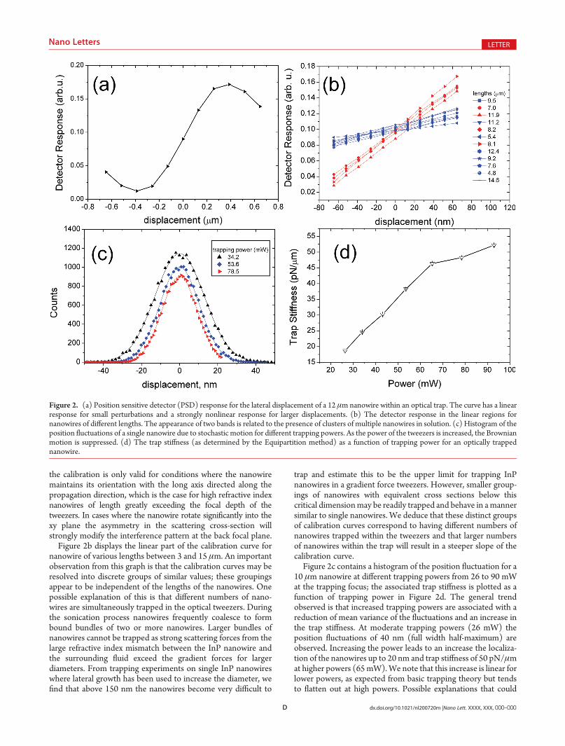
In Figure 3a we consider the dependence of the trap stiffnessversus nanowire length, as determined by the equipartition meth-od. From the plots we can see that the results can again be dividedinto distinct bands of different values. The average value for thepoints in the lower band is 0.71( 0.24 pN μm�1 mW�1, and theaverage of the points in the upper band is 2.02( 0.20 pN μm�1
mW�1. Within one band we see that the trap stiffness of thenanowires is again independent of the length of the nanowires.Importantly, the wires with trap stiffness that fall into the upperband of stiffness values corresponds to the same wires with thelarger slope in the calibration curves. This strongly suggests thatthe nanowires with larger slopes in the calibration curve andlarger trap stiffness values are actually two nanowires. Intuitively,one would expect that for a given trapping laser power, the trapstiffness of the optical trap would depend on the length of thetrapped nanowires. However, the observed length independencemay be rationalized by considering the depth of focus of the opticaltweezers. As the length of the nanowires extends far beyond thedepth of focus of the microscope objective (∼1.0 μm), but withthe gradient forces only dominate within the depth of focus, any
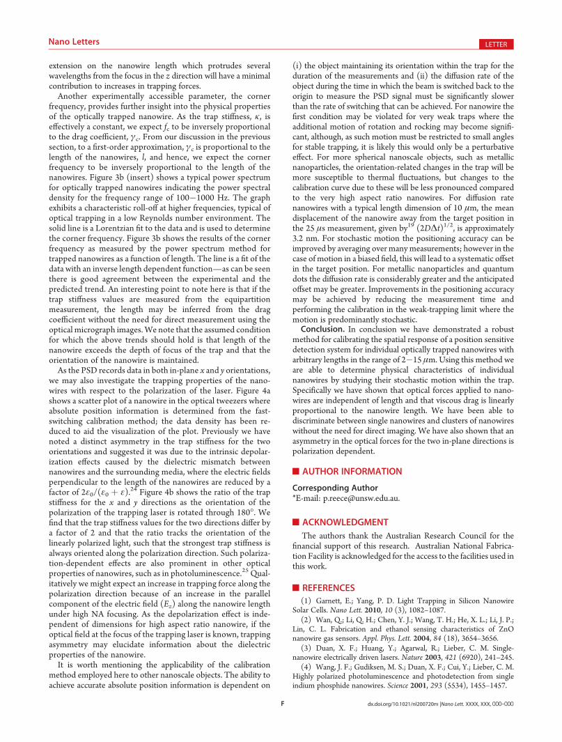
Figure 3. (a) Trap stiffness as function of the nanowire length, asdetermined using the equipartion method. The appearance of two bandsis related to the presence of multiple nanowires in the trap. The indepen-dence of the trapping force with respect to the length may be rationalized interms of the depth of focus of the beam. (b) Corner frequency of trappednanowires as a function of the nanowire length, as determined by a powerspectrum analysis. The corner frequency exhibits a one on length depen-dence that may be linked to the Stokes’ drag perpendicular to the length ofthe nanowire.
Figure 4. (a) Scatter plot showing the position fluctuation of thenanowire in the trap. A clear asymmetry in the distribution is observedwhen comparing the x and y axis. This asymmetry translates to a differencein the trap stiffness for the two orientations. (b) Ratio of the trap stiffnessin the x and y directions as a function of polarization orientation. Theasymmetry in the trapping ratio changes with the orientation such that thelargest trap stiffness is always in line with the direction of polarization.
F dx.doi.org/10.1021/nl200720m |Nano Lett. XXXX, XXX, 000–000
Nano Letters LETTER
extension on the nanowire length which protrudes severalwavelengths from the focus in the z direction will have a minimalcontribution to increases in trapping forces.Another experimentally accessible parameter, the corner
frequency, provides further insight into the physical propertiesof the optically trapped nanowire. As the trap stiffness, κ, iseffectively a constant, we expect fc to be inversely proportionalto the drag coefficient, γc. From our discussion in the previoussection, to a first-order approximation, γc is proportional to thelength of the nanowires, l, and hence, we expect the cornerfrequency to be inversely proportional to the length of thenanowires. Figure 3b (insert) shows a typical power spectrumfor optically trapped nanowires indicating the power spectraldensity for the frequency range of 100�1000 Hz. The graphexhibits a characteristic roll-off at higher frequencies, typical ofoptical trapping in a low Reynolds number environment. Thesolid line is a Lorentzian fit to the data and is used to determinethe corner frequency. Figure 3b shows the results of the cornerfrequency as measured by the power spectrum method fortrapped nanowires as a function of length. The line is a fit of thedata with an inverse length dependent function—as can be seenthere is good agreement between the experimental and thepredicted trend. An interesting point to note here is that if thetrap stiffness values are measured from the equipartitionmeasurement, the length may be inferred from the dragcoefficient without the need for direct measurement using theoptical micrograph images. We note that the assumed conditionfor which the above trends should hold is that length of thenanowire exceeds the depth of focus of the trap and that theorientation of the nanowire is maintained.As the PSD records data in both in-plane x and y orientations,
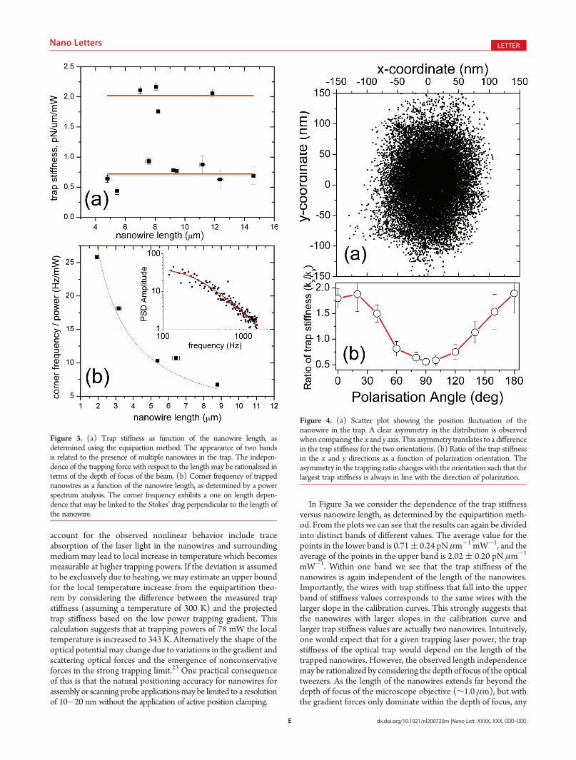
we may also investigate the trapping properties of the nano-wires with respect to the polarization of the laser. Figure 4ashows a scatter plot of a nanowire in the optical tweezers whereabsolute position information is determined from the fast-switching calibration method; the data density has been re-duced to aid the visualization of the plot. Previously we havenoted a distinct asymmetry in the trap stiffness for the twoorientations and suggested it was due to the intrinsic depolar-ization effects caused by the dielectric mismatch betweennanowires and the surrounding media, where the electric fieldsperpendicular to the length of the nanowires are reduced by afactor of 2ε0/(ε0 þ ε).24 Figure 4b shows the ratio of the trapstiffness for the x and y directions as the orientation of thepolarization of the trapping laser is rotated through 180�. Wefind that the trap stiffness values for the two directions differ bya factor of 2 and that the ratio tracks the orientation of thelinearly polarized light, such that the strongest trap stiffness isalways oriented along the polarization direction. Such polariza-tion-dependent effects are also prominent in other opticalproperties of nanowires, such as in photoluminescence.25 Qual-itatively we might expect an increase in trapping force along thepolarization direction because of an increase in the parallelcomponent of the electric field (Ez) along the nanowire lengthunder high NA focusing. As the depolarization effect is inde-pendent of dimensions for high aspect ratio nanowire, if theoptical field at the focus of the trapping laser is known, trappingasymmetry may elucidate information about the dielectricproperties of the nanowire.It is worth mentioning the applicability of the calibration
method employed here to other nanoscale objects. The ability toachieve accurate absolute position information is dependent on
(i) the object maintaining its orientation within the trap for theduration of the measurements and (ii) the diffusion rate of theobject during the time in which the beam is switched back to theorigin to measure the PSD signal must be significantly slowerthan the rate of switching that can be achieved. For nanowire thefirst condition may be violated for very weak traps where theadditional motion of rotation and rocking may become signifi-cant, although, as such motion must be restricted to small anglesfor stable trapping, it is likely this would only be a perturbativeeffect. For more spherical nanoscale objects, such as metallicnanoparticles, the orientation-related changes in the trap will bemore susceptible to thermal fluctuations, but changes to thecalibration curve due to these will be less pronounced comparedto the very high aspect ratio nanowires. For diffusion ratenanowires with a typical length dimension of 10 μm, the meandisplacement of the nanowire away from the target position inthe 25 μs measurement, given by19 (2DΔt)1/2, is approximately3.2 nm. For stochastic motion the positioning accuracy can beimproved by averaging over manymeasurements; however in thecase of motion in a biased field, this will lead to a systematic offsetin the target position. For metallic nanoparticles and quantumdots the diffusion rate is considerably greater and the anticipatedoffset may be greater. Improvements in the positioning accuracymay be achieved by reducing the measurement time andperforming the calibration in the weak-trapping limit where themotion is predominantly stochastic.Conclusion. In conclusion we have demonstrated a robust
method for calibrating the spatial response of a position sensitivedetection system for individual optically trapped nanowires witharbitrary lengths in the range of 2�15 μm. Using this method weare able to determine physical characteristics of individualnanowires by studying their stochastic motion within the trap.Specifically we have shown that optical forces applied to nano-wires are independent of length and that viscous drag is linearlyproportional to the nanowire length. We have been able todiscriminate between single nanowires and clusters of nanowireswithout the need for direct imaging. We have also shown that anasymmetry in the optical forces for the two in-plane directions ispolarization dependent.
’AUTHOR INFORMATION
Corresponding Author*E-mail: [email protected].
’ACKNOWLEDGMENT
The authors thank the Australian Research Council for thefinancial support of this research. Australian National Fabrica-tion Facility is acknowledged for the access to the facilities used inthis work.
’REFERENCES
(1) Garnett, E.; Yang, P. D. Light Trapping in Silicon NanowireSolar Cells. Nano Lett. 2010, 10 (3), 1082–1087.
(2) Wan, Q.; Li, Q. H.; Chen, Y. J.; Wang, T. H.; He, X. L.; Li, J. P.;Lin, C. L. Fabrication and ethanol sensing characteristics of ZnOnanowire gas sensors. Appl. Phys. Lett. 2004, 84 (18), 3654–3656.
(3) Duan, X. F.; Huang, Y.; Agarwal, R.; Lieber, C. M. Single-nanowire electrically driven lasers. Nature 2003, 421 (6920), 241–245.
(4) Wang, J. F.; Gudiksen, M. S.; Duan, X. F.; Cui, Y.; Lieber, C. M.Highly polarized photoluminescence and photodetection from singleindium phosphide nanowires. Science 2001, 293 (5534), 1455–1457.

G dx.doi.org/10.1021/nl200720m |Nano Lett. XXXX, XXX, 000–000
Nano Letters LETTER
(5) Huang, Y.; Duan, X. F.; Cui, Y.; Lauhon, L. J.; Kim, K. H.; Lieber,C. M. Logic gates and computation from assembled nanowire buildingblocks. Science 2001, 294 (5545), 1313–1317.(6) Yan, H.; Choe, H. S.; Nam, S. W.; Hu, Y. J.; Das, S.; Klemic, J. F.;
Ellenbogen, J. C.; Lieber, C. M. Programmable nanowire circuits fornanoprocessors. Nature 2011, 470 (7333), 240–244.(7) Lauhon, L. J.; Gudiksen, M. S.; Wang, C. L.; Lieber, C. M.
Epitaxial core-shell and core-multishell nanowire heterostructures.Nature 2002, 420 (6911), 57–61.(8) Pauzauskie, P. J.; Radenovic, A.; Trepagnier, E.; Shroff, H.; Yang,
P. D.; Liphardt, J. Optical trapping and integration of semiconductornanowire assemblies in water. Nat. Mater. 2006, 5 (2), 97–101.(9) Reece, P. J.; Paiman, S.; Abdul-Nabi, O.; Gao, Q.; Gal, M.; Tan,
H. H.; Jagadish, C. Combined optical trapping and microphotolumines-cence of single InP nanowires. Appl. Phys. Lett. 2009, 95 (10), 101109.(10) Agarwal, R.; Ladavac, K.; Roichman, Y.; Yu, G. H.; Lieber,
C. M.; Grier, D. G. Manipulation and assembly of nanowires withholographic optical traps. Opt. Express 2005, 13 (22), 8906–8912.(11) Neuman, K. C.; Block, S. M. Optical trapping. Rev. Sci. Instrum.
2004, 75 (9), 2787–2809.(12) Berg-Sorensen, K.; Flyvbjerg, H. Power spectrum analysis for
optical tweezers. Rev. Sci. Instrum. 2004, 75 (3), 594–612.(13) Greenleaf, W. J.; Woodside, M. T.; Abbondanzieri, E. A.; Block,
S. M. Passive all-optical force clamp for high-resolution laser trapping.Phys. Rev. Lett. 2005, 95 (20), 208102.(14) Visscher, K.; Gross, S. P.; Block, S. M. Construction of multiple-
beam optical traps with nanometer-resolution position sensing. IEEE J.Sel. Top. Quantum Electron. 1996, 2 (4), 1066–1076.(15) Joyce, H. J.; Paiman, S.; Gao, Q.; Tan, H. H.; Kim, Y.; Smith,
L.M.; Jackson, H. E.; Yarrison-Rice, J.M.; Zhang, X.; Zou, J.; Jagadish, C.III-V Compound Semiconductor Nanowires. Nanotechnology Materialsand Devices Conference, 2009. NMDC '09; IEEE: New York, 2009; pp59�60(16) Wagner, R. S.; Ellis, W. C. Vapor-Liquid-Solid Mechanism of
Single Crystal Growth (New Method Growth Catalysis from ImpurityWhisker Epitaxial þ Large Crystals Si E). Appl. Phys. Lett. 1964, 4 (5),89.(17) Paiman, S.;Growth temperature and V/III ratio effects on the
morphology and crystal structure of InP nanowires. J. Phys. D: Appl.Phys.2010, 43 (44), 445402.(18) Dholakia, K.; Reece, P.; Gu, M. Optical micromanipulation.
Chem. Soc. Rev. 2008, 37 (1), 42–55.(19) Risken, H. The Fokker-Planck equation: methods of solution and
applications. 2nd ed.; Springer-Verlag: Berlin and New York, 1989.(20) Marago, O. M.; Jones, P. H.; Bonaccorso, F.; Scardaci, V.;
Gucciardi, P. G.; Rozhin, A. G.; Ferrari, A. C. Femtonewton ForceSensing with Optically Trapped Nanotubes. Nano Lett. 2008, 8 (10),3211–3216.(21) Tirado, M. M.; Garciadelatorre, J. Translational Friction Coef-
ficients of Rigid, Symmetric Top Macromolecules - Application toCircular-Cylinders. J. Chem. Phys. 1979, 71 (6), 2581–2587.(22) Rohrbach, A.; Kress, H.; Stelzer, E. H. K. Three-dimensional
tracking of small spheres in focused laser beams: influence of thedetection angular aperture. Opt. Lett. 2003, 28 (6), 411–413.(23) Roichman, Y.; Sun, B.; Stolarski, A.; Grier, D. G. Influence of
nonconservative optical forces on the dynamics of optically trappedcolloidal spheres: The fountain of probability. Phys. Rev. Lett. 2008, 101(12), 128301.(24) Ruda, H. E.; Shik, A. Polarization-sensitive optical phenomena
in semiconducting and metallic nanowires. Phys. Rev. B 2005, 72 (11),115308.(25) Mishra, A.; Titova, L. V.; Hoang, T. B.; Jackson, H. E.; Smith,
L. M.; Yarrison-Rice, J. M.; Kim, Y.; Joyce, H. J.; Gao, Q.; Tan, H. H.;Jagadish, C. Polarization and temperature dependence of photolumi-nescence from zincblende and wurtzite InP nanowires. Appl. Phys. Lett.2007, 91 (26), 263104.