SEMICONDUCTOR PRODUCTS
69
SEMICONDUCTOR PRODUCTS SHORT FORM CATALOG 2015
-
Upload
khangminh22 -
Category
Documents
-
view
1 -
download
0
Transcript of SEMICONDUCTOR PRODUCTS
SEMICONDUCTOR PRODUCTS
SHORT FORM CATALOG
2015
INTEGRAL JSC reserves the right to make changes in device design, specifications and other information identified in this publication without notice and assumes no responsibility for the use of any device described herein.
INTEGRAL JSC advices its customers to obtain the latest version of relevant information to verify before placing orders, that the information being relied upon is current.
Reference to products of other manufacturers are solely for convenience and do not imply total equivalency of design, performance, or otherwise.
Copyright © 2015, INTEGRAL JSC, Republic of Belarus
3
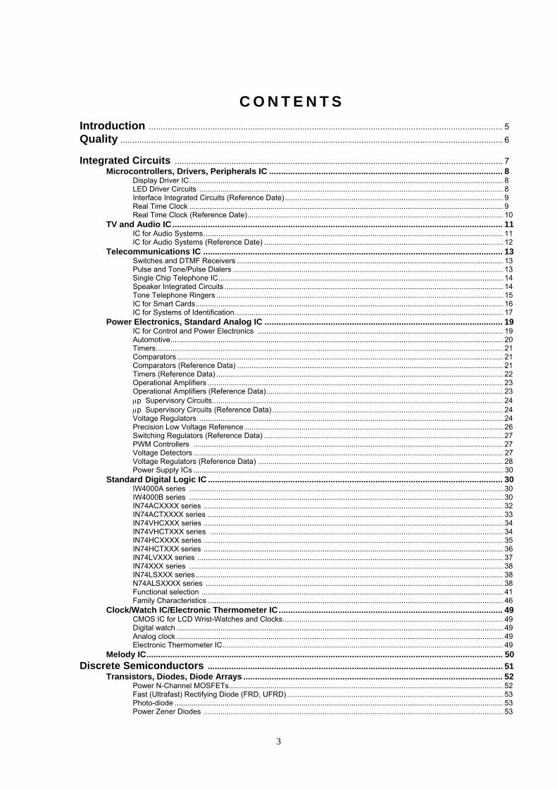
C O N T E N T S
Introduction ...................................................................................................................................................... 5 Quality .................................................................................................................................................................. 6 Integrated Circuits ........................................................................................................................................... 7
Microcontrollers, Drivers, Peripherals IC ................................................................................................... 8 Display Driver IC ....................................................................................................................................................... 8 LED Driver Circuits .................................................................................................................................................. 8 Interface Integrated Circuits (Reference Date) ......................................................................................................... 9 Real Time Clock ....................................................................................................................................................... 9 Real Time Clock (Reference Date) ........................................................................................................................... 10
TV and Audio IC ............................................................................................................................................ 11 IC for Audio Systems ................................................................................................................................................ 11 IC for Audio Systems (Reference Date) ................................................................................................................... 12
Telecommunications IC ............................................................................................................................... 13 Switches and DTMF Receivers ................................................................................................................................ 13 Pulse and Tone/Pulse Dialers .................................................................................................................................. 13 Single Chip Telephone IC ......................................................................................................................................... 14 Speaker Integrated Circuits ...................................................................................................................................... 14 Tone Telephone Ringers .......................................................................................................................................... 15 IC for Smart Cards .................................................................................................................................................... 16 IС for Systems of Identification ................................................................................................................................. 17
Power Electronics, Standard Analog IC ..................................................................................................... 19 IC for Control and Power Electronics ...................................................................................................................... 19 Automotive ................................................................................................................................................................ 20 Timers ....................................................................................................................................................................... 21 Comparators ............................................................................................................................................................. 21 Comparators (Reference Data) ................................................................................................................................ 21 Timers (Reference Data) .......................................................................................................................................... 22 Operational Amplifiers .............................................................................................................................................. 23 Operational Amplifiers (Reference Data) .................................................................................................................. 23 μp Supervisory Circuits ............................................................................................................................................ 24 μp Supervisory Circuits (Reference Data) ............................................................................................................... 24 Voltage Regulators .................................................................................................................................................. 24 Precision Low Voltage Reference ............................................................................................................................ 26 Switching Regulators (Reference Data) ................................................................................................................... 27 PWM Controllers ..................................................................................................................................................... 27 Voltage Detectors ..................................................................................................................................................... 27 Voltage Regulators (Reference Data) ...................................................................................................................... 28 Power Supply ICs ..................................................................................................................................................... 30
Standard Digital Logic IC ............................................................................................................................. 30 IW4000A series ....................................................................................................................................................... 30 IW4000B series ....................................................................................................................................................... 30 IN74ACXXXX series ................................................................................................................................................ 32 IN74ACTXXXX series .............................................................................................................................................. 33 IN74VHCXXX series ................................................................................................................................................ 34 IN74VHCTXXX series ............................................................................................................................................. 34 IN74HCXXXX series ................................................................................................................................................ 35 IN74HCTXXX series ................................................................................................................................................ 36 IN74LVXXX series ................................................................................................................................................... 37 IN74XXX series ....................................................................................................................................................... 38 IN74LSXXX series .................................................................................................................................................... 38 N74ALSXXXX series ............................................................................................................................................... 38 Functional selection ................................................................................................................................................. 41 Family Characteristics .............................................................................................................................................. 46
Clock/Watch IC/Electronic Thermometer IC ............................................................................................... 49 CMOS IC for LCD Wrist-Watches and Clocks .......................................................................................................... 49 Digital watch ............................................................................................................................................................. 49 Analog clock ............................................................................................................................................................. 49 Electronic Thermometer IC ....................................................................................................................................... 49
Melody IC ....................................................................................................................................................... 50 Discrete Semiconductors ............................................................................................................................. 51
Transistors, Diodes, Diode Arrays .............................................................................................................. 52 Power N-Channel MOSFETs.................................................................................................................................... 52 Fast (Ultrafast) Rectifying Diode (FRD, UFRD) ........................................................................................................ 53 Photo-diode .............................................................................................................................................................. 53 Power Zener Diodes ................................................................................................................................................ 53

4
Fast (Ultrafast) Rectifying Diode Arrays (FRDA, UFRDA) ....................................................................................... 53 Bipolar Transistors .................................................................................................................................................. 54 Unijunction Transistors ............................................................................................................................................. 54 Power Thyristors and Triacs ..................................................................................................................................... 54
Foundry-business ................................................................................................................................ 55 Base Technology Process ........................................................................................................................................ 56
Contacts ............................................................................................................................................................... 69
5
INTRODUCTION «INTEGRAL» JSC develops, manufactures and exports microelectronic components
and electronic products. «INTEGRAL» JSC provides a full cycle of design and manufacture: from silicon substrates up to integrated circuits and semiconductor devices, from microelectronic components up to electronic.
Total labour is more than 6 thousand persons. Mr. Vitaly A. Solodukha has been the General Director of «INTEGRAL» JSC. The main line of activity of «INTEGRAL» JSC is design and manufacture of
microelectronic products - over 70 % of the total production volume - for the branches manufacturing goods of household and consumer electronics.
«INTEGRAL» JSC exports more than 70 % of the volume of manufactured goods to the markets of the Russian Federation, Sout - East Asia, India and Western Europe.
The goods are exported to 30 countries of the world. Manufacture of 0,35 µт design rule integrated circuits on Ø200 mm (8 inch) wafers
has been set up. The main lines of the development of «INTEGRAL» JSC are as follows: design and
implementation of microelectronic components of power electronics, microsensorics and optoelectronics.
Development of production of finished electronics is to be carried out in the following lines: displays; automotive electronics and electronics and equipment for health application; cashless payment systems, payment terminals, commercial and bank equipment, smart cards, identification and record keeping systems.
«INTEGRAL» JSC is open for cooperation both in design and deliveries of products, and in terms of joint realization of long-term investment projects.
• BASIC TYPES OF INTEGRATED CIRCUITS MANUFACTURED: - Memories - Microcontrollers, drivers, peripheral IC - TV and audio IC - Telecommunications IC - Power electronics, standard analog IC
- Standard digital logic IC - Special-purpose electronic component base - Clock/watch, calculator IC
- Music synthesizer and electronic thermometer IC
• BASIC TYPES OF SEMICONDUCTOR DEVICES MANUFACTURED: - Bipolar transistors - Power bipolar Darlington transistors - Insulated gate bipolar transistors - Bipolar transistors with integrated anti-saturating element - Bipolar transistors with damping diode and resistor in the emitter-base circuit - Unijunction bipolar transistors - Low-power n- and p-channel MOSFETs
- Power n- and p-channel MOSFETs - Microwave mixing diodes, rectifier diodes, Schottky diodes - Power high-speed diodes and diode matrices - Pulse diode matrices - Power rectifier and limiter diodes

6
QUALITY MANAGEMENT SYSTEM
The Quality Management System of "INTEGRAL" was established more than 15 years ago, and in 1999 it was certified by "KEMA", the International Certification Center, and by "BelGISS", the National Certification Center, for compliance with ISO 9001.
The main objective of the Quality Management System is to integrate the efforts of all employees for design, manufacture and sale of high quality, competitive and technologically advanced integrated circuits, semiconductor devices, liquid crystal displays and other products maximally meeting the requirements and demands of consumers.
At present, the Quality Management System of "INTEGRAL" JSC, covers design, manufacture and supply of integrated circuits, semiconductor devices and liquid crystal displays and meets the requirements of ISO 9001 -2009 in the National System of the Republic of Belarus and DIN EN ISO 9001:2008 of the foreign certification organization DAkkS, Germany. The Quality Management System of single-crystal silicon wafer complies with the requirements of ISO 9001:2009 Standard of the Republic of Belarus.
INTEGRATED CIRCUITS
INTEGRATED CIRCUITS Microcontrollers, Drivers, Peripherals IC
8
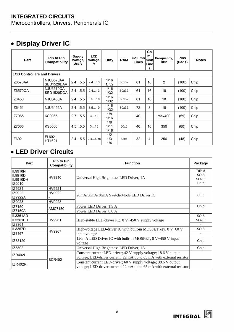
• Display Driver IC
Part Pin to Pin Compatibility
Supply Voltage,
Ucc,V
LCD Voltage,
V Duty RAM Column
Lines
Com-
mon Line
s
Fre-quency, kHz
Pins (Pads) Notes
LCD Controllers and Drivers
IZ6570AA NJU6570AA SED1520DAA 2.4…5.5 2.4…13 1/16
1/ 32 80x32 61 16 2 (100) Chip
IZ6570OA NJU6570OA SED1520DOA 2.4…5.5 2.4…13 1/16
1/32 80x32 61 16 18 (100) Chip
IZ6450 NJU6450A 2.4…5.5 3.5…10 1/16 1/32 80x32 61 16 18 (100) Chip
IZ6451 NJU6451A 2.4…5.5 3.5…10 1/16 1/32 80x32 72 8 18 (100) Chip
IZ7065 KS0065 2.7…5.5 3…13 1/8 1/16 40 max400 (59) Chip
IZ7066 KS0066 4.5…5.5 3…13 1/8 1/11 1/16
80x8 40 16 350 (80) Chip
IZ602 FL602 HT1621 2.4…5.5 2.4…Ucc
1/2 1/3 1/4
32x4 32 4 256 (48) Chip
• LED Driver Circuits Part Pin to Pin
Compatibility Function Package
IL9910N IL9910D IL9910DH IZ9910
HV9910 Universal High Brightness LED Driver, 1A
DIP-8 SO-8 SO-16 Chip
IZ9921 HV9921
20mA/50mA/30mA Switch-Mode LED Driver IC Chip IZ9922 HV9922 IZ9922A - IZ9923 HV9923 IZ7150 IZ7150A AMC7150 Power LED Driver, 1,5 A Chip
Power LED Driver, 0,8 A IL3361AD
HV9961 High-stable LED-driver IC; 8 V÷450 V supply voltage SO-8
IL3361BD SO-16 IZ3361 - IL3367D
HV9967 High-voltage LED-driver IC with built-in MOSFET key, 8 V÷60 V input voltage
SO-8 IZ3367 -
IZ33120 120mA LED Driver IC with built-in MOSFET, 8 V÷450 V input voltage Chip
IZ3302 Universal High Brightness LED Driver, 1A Chip
IZR402U BCR402
Constant current LED-driver; 42 V supply voltage; 18.6 V output voltage; LED-driver current: 22 mA up to 65 mA with external resistor
IZR402R Constant current LED-driver; 60 V supply voltage; 38.6 V output voltage; LED-driver current: 22 mA up to 65 mA with external resistor
INTEGRATED CIRCUITS Microcontrollers, Drivers, Peripherals IC
9
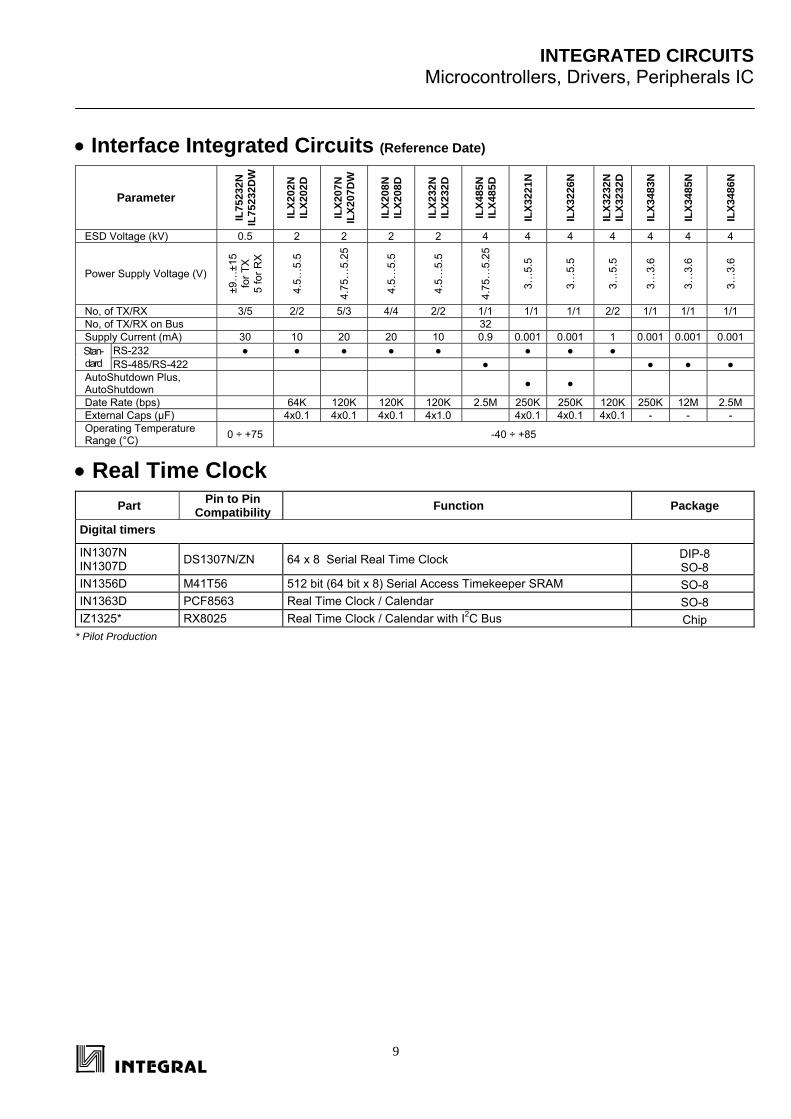
• Interface Integrated Circuits (Reference Date)
Parameter
IL75
232N
IL
7523
2DW
ILX2
02N
IL
X202
D
ILX2
07N
IL
X207
DW
ILX2
08N
IL
X208
D
ILX2
32N
IL
X232
D
ILX4
85N
IL
X485
D
ILX3
221N
ILX3
226N
ILX3
232N
IL
X323
2D
ILX3
483N
ILX3
485N
ILX3
486N
ESD Voltage (kV) 0.5 2 2 2 2 4 4 4 4 4 4 4
Power Supply Voltage (V)
±9…
±15
for T
X
5 fo
r RX
4.5…
5.5
4.75
…5.
25
4.5…
5.5
4.5…
5.5
4.75
…5.
25
3…5.
5
3…5.
5
3…5.
5
3…3.
6
3…3.
6
3…3.
6
No, of TX/RX 3/5 2/2 5/3 4/4 2/2 1/1 1/1 1/1 2/2 1/1 1/1 1/1 No, of TX/RX on Bus 32 Supply Current (mA) 30 10 20 20 10 0.9 0.001 0.001 1 0.001 0.001 0.001 Stan- dard
RS-232 ● ● ● ● ● ● ● ● RS-485/RS-422 ● ● ● ●
AutoShutdown Plus, AutoShutdown ● ●
Date Rate (bps) 64K 120K 120K 120K 2.5M 250K 250K 120K 250K 12M 2.5M External Caps (µF) 4x0.1 4x0.1 4x0.1 4x1.0 4x0.1 4x0.1 4x0.1 - - - Operating Temperature Range (°С) 0 ÷ +75 -40 ÷ +85
• Real Time Clock Part Pin to Pin
Compatibility Function Package
Digital timers
IN1307N IN1307D DS1307N/ZN 64 x 8 Serial Real Time Clock DIP-8
SO-8 IN1356D M41T56 512 bit (64 bit x 8) Serial Access Timekeeper SRAM SO-8 IN1363D PCF8563 Real Time Clock / Calendar SO-8 IZ1325* RX8025 Real Time Clock / Calendar with I2C Bus Chip
* Pilot Production
INTEGRATED CIRCUITS Microcontrollers, Drivers, Peripherals IC
10
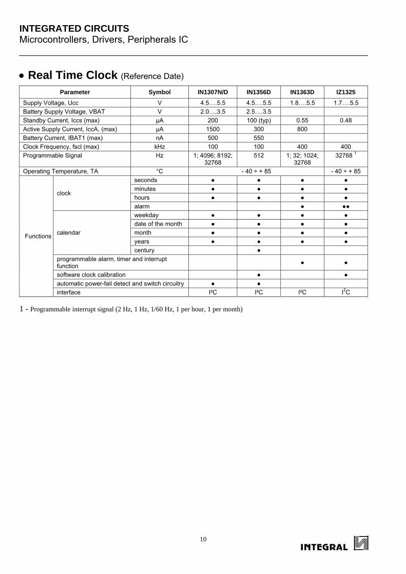
• Real Time Clock (Reference Date) Parameter Symbol IN1307N/D IN1356D IN1363D IZ1325
Supply Voltage, Ucc V 4.5….5.5 4.5….5.5 1.8.…5.5 1.7….5.5 Battery Supply Voltage, VBAT V 2.0….3.5 2.5….3.5 Standby Current, Iccs (max) µА 200 100 (typ) 0.55 0.48 Active Supply Current, IccA, (max) µА 1500 300 800 Battery Current, IBAT1 (max) nА 500 550 Clock Frequency, fscl (max) kHz 100 100 400 400 Programmable Signal Hz 1; 4096; 8192;
32768 512 1; 32; 1024;
32768 32768 1
Operating Temperature, TA °C - 40 ÷ + 85 - 40 ÷ + 85
Functions
clock
seconds ● ● ● ● minutes ● ● ● ● hours ● ● ● ● alarm ● ●●
calendar
weekday ● ● ● ● date of the month ● ● ● ● month ● ● ● ● years ● ● ● ● century ●
programmable alarm, timer and interrupt function ● ●
software clock calibration ● ● automatic power-fail detect and switch circuitry ● ● interface I²C I²C I²C I2C
1 - Programmable interrupt signal (2 Hz, 1 Hz, 1/60 Hz, 1 per hour, 1 per month)
INTEGRATED CIRCUITS TV and Audio IC
11
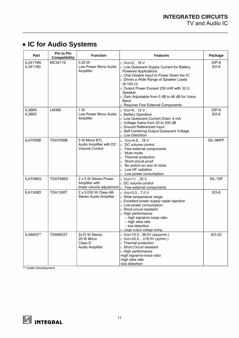
• IC for Audio Systems Part Pin to Pin
Compatibility Function Features Package
IL34119N IL34119D
MC34119 0.25 W Low Power Mono Audio Amplifier
Vcc=2…16 V Low Quiescent Supply Current for Battery Powered Applications Chip Disable Input to Power Down the IC Drives a Wide Range of Speaker Loads (8-100 Ω) Output Power Exceed 250 mW with 32 Ω Speaker Gain Adjustable from 0 dB to 46 dB for Voice Band Requires Few External Components
DIP-8 SO-8
IL386N IL386D
LM386 1 W Low Power Mono Audio Amplifier
Vcc=4…12 V Battery Operation Low Quiescent Current Drain: 4 mA Voltage Gains from 20 to 200 dB Ground Referenced Input Self-Centering Output Quiescent Voltage Low Distortion
DIP-8 SO-8
ILA7056B TDA7056B 5 W Mono BTL Audio Amplifier with DC Volume Control
Vcc=4.5…18 V DC volume control Few external components Mute mode Thermal protection Short-circuit proof No switch-on and of clicks Low HF radiation Low power consumption
SIL-9MPF
ILA7496Q TDA7496Q 2 x 5 W Stereo Power Amplifier with linear volume adjustment
Vcc=11…35 V DC volume control Few external components
SIL-15P
ILA1308D TDA1308Т 2 x 0.030 W Class AB Stereo Audio Amplifier
Vcc=3.0…7.0 V Wide temperature range Excellent power supply ripple rejection Low power consumption Short-circuit resistant High performance
– high signal-to-noise ratio – high slew rate – low distortion
Large output voltage swing
SO-8
ILA8933** TDA8933T 2x10 W Stereo 20 W Mono Class D Audio Amplifier
Vcc=10.0...36.0V (assymm.) Vcc=±5.0... ±18.0V (symm.) Thermal protection Short Circuit resistant High performance
-high signal-to-noice ratio -high slew rate -low distortion
SO-32
** Under Development
INTEGRATED CIRCUITS TV and Audio IC
12
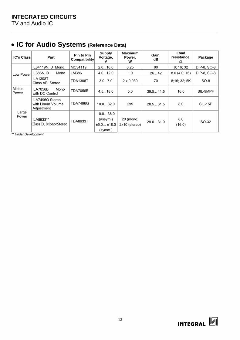
• IC for Audio Systems (Reference Data)
IC’s Class Part Pin to Pin Compatibility
Supply Voltage,
V
Maximum Power,
W Gain,
dB
Load resistance,
Ω Package
Low Power
IL34119N, D Mono MC34119 2.0...16.0 0.25 80 8; 16; 32 DIP-8, SO-8 IL386N, D Mono LM386 4.0...12.0 1.0 26…42 8.0 (4.0; 16) DIP-8, SO-8 ILA1308Т Class AB, Stereo TDA1308Т 3.0...7.0 2 x 0.030 70 8;16; 32; 5K SO-8
Middle Power
ILA7056B Mono with DC Control
TDA7056B 4.5...18.0 5.0 39.5…41.5 16.0 SIL-9MPF
Large Power
ILA7496Q Stereo with Linear Volume Adjustment
TDA7496Q 10.0…32.0 2х5 28.5…31.5 8.0 SIL-15P
ILA8933** Class D, Mono/Stereo
TDA8933T
10.0…36.0 (assym.)
±5.0... ±18.0(symm.)
20 (mono) 2x10 (stereo)
29.0…31.0 8.0
(16.0) SO-32
** Under Development
INTEGRATED CIRCUITS Telecommunications IC
13
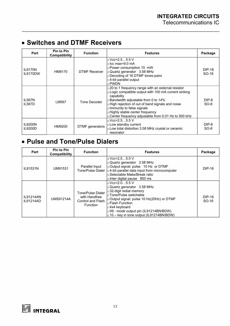
• Switches and DTMF Receivers Part Pin to Pin
Compatibility Function Features Package
IL9170N IL9170DW HM9170 DTMF Receiver
Vcc=2.5…5.5 V Icc max=9.0 mA Power consumption 15 mW Quartz generator 3.58 MHz Decoding of 16 DTMF tones-pairs 4-bit parallel output PWDN
DIP-18 SO-18
IL567N IL567D LM567 Tone Decoder
20 to 1 frequency range with an external resistor Logic compatible output with 100 mA current sinking capability Bandwidth adjustable from 0 to 14% High rejection of out of band signals and noise Immunity to false signals Highly stable center frequency Center frequency adjustable from 0.01 Hz to 500 kHz
DIP-8 SO-8
IL9200N IL9200D HM9200 DTMF generators
Vcc=2.5…5.5 V Low standby current Low total distortion 3.58 MHz crystal or ceramic resonator
DIP-8 SO-8
• Pulse and Tone/Pulse Dialers Part Pin to Pin
Compatibility Function Features Package
IL91531N UM91531 Parallel Input Tone/Pulse Dialer
Vcc=2.5…5.5 V Quartz generator 3.58 MHz Output signal: pulse 10 Hz or DTMF 4-bit parallel data input from microcomputer Selectable Make/Break ratio Inter digital pause 800 ms
DIP-16
IL91214AN IL91214AD UMS91214A
Tone/Pulse Dialer with Handfree
Control and Flash Function
Vcc=2.0…5.5 V Quartz generator 3.58 MHz 32-digit redial memory Tone/Pulse switchable Output signal: pulse 10 Hz(20Hz) or DTMF Flash Function 4x4 keyboard 09 - mode output pin (IL91214BN/BDW) 10 – key in tone output (IL91214BN/BDW)
DIP-16 SO-16
INTEGRATED CIRCUITS Telecommunications IC
14
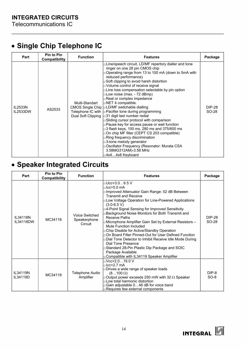
• Single Chip Telephone IC Part Pin to Pin
Compatibility Function Features Package
IL2533N IL2533DW AS2533
Multi-Standart CMOS Single Chip Telephone IC with Dual Soft Clipping
Line/speech circuit, LD/MF repertory dialler and tone ringer on one 28 pin CMOS chip Operating range from 13 to 100 mA (down to 5mA with reduced performance) Soft clipping to avoid harsh distortion Volume control of receive signal Line loss compensation selectable by pin option Low noise (max. - 72 dBmp) Real or complex impedance NET 4 compatible. LD/MF switchable dialling Pacifier tone during programming 31 digit last number redial Sliding cursor protocol with comparison Pause key for access pause or wait function 3 flash keys, 100 ms, 280 ms and 375/600 ms On chip MF filter (CEPT CS 203 compatible) Ring frequency discrimination 3-tone melody generator Oscillator Frequency (Resonator: Murata CSA 3.58MG312AM)-3.58 MHz 4х4…4х8 Keyboard
DIP-28 SO-28
• Speaker Integrated Circuits Part Pin to Pin
Compatibility Function Features Package
IL34118N IL34118DW MC34118
Voice Switched Speakerphone
Circuit
Ucс=3.0…6.5 V Icc=5.0 mA Improved Attenuator Gain Range: 52 dB Between Transmit and Receive Low Voltage Operation for Line-Powered Applications (3.0-6.5 V) 4-Point Signal Sensing for Improved Sensitivity Background Noise Monitors for Both Transmit and Receive Paths Microphone Amplifier Gain Set by External Resistors – Mute Function Included Chip Disable for Active/Standby Operation On Board Filter Pinned-Out for User Defined Function Dial Tone Detector to Inhibit Receive Idle Mode During Dial Tone Presence Standard 28-Pin Plastic Dip Package and SOIC Package Available Compatible with IL34119 Speaker Amplifier
DIP-28 SO-28
IL34119N IL34119D MC34119 Telephone Audio
Amplifier
Vcc=2.0…16.0 V Icc=2.7 mA Drives a wide range of speaker loads (8…100 Ω) Output power exceeds 250 mW with 32 Ω Speaker Low total harmonic distortion Gain adjustable 0…46 dB for voice band Requires few external components
DIP-8 SO-8
INTEGRATED CIRCUITS Telecommunications IC
15
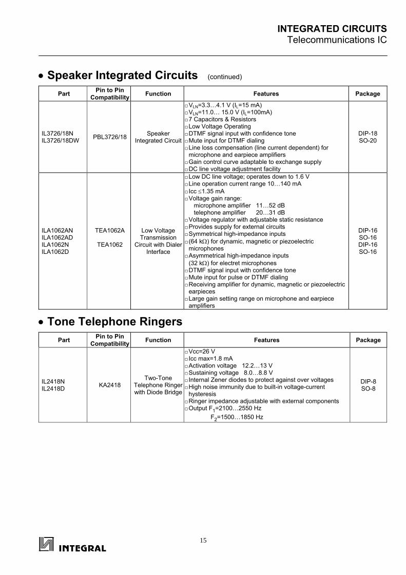
• Speaker Integrated Circuits (continued) Part Pin to Pin
Compatibility Function Features Package
IL3726/18N IL3726/18DW PBL3726/18 Speaker
Integrated Circuit
VLN=3.3…4.1 V (IL=15 mA) VLN=11.0… 15.0 V (IL=100mA) 7 Capacitors & Resistors Low Voltage Operating DTMF signal input with confidence tone Mute input for DTMF dialing Line loss compensation (line current dependent) for microphone and earpiece amplifiers Gain control curve adaptable to exchange supply DC line voltage adjustment facility
DIP-18 SO-20
ILA1062AN ILA1062AD ILA1062N ILA1062D
TEA1062A
TEA1062
Low Voltage Transmission
Circuit with Dialer Interface
Low DC line voltage; operates down to 1.6 V Line operation current range 10…140 mA Icc ≤1.35 mA Voltage gain range: microphone amplifier 11…52 dB telephone amplifier 20…31 dB Voltage regulator with adjustable static resistance Provides supply for external circuits Symmetrical high-impedance inputs (64 kΩ) for dynamic, magnetic or piezoelectric microphones Asymmetrical high-impedance inputs (32 kΩ) for electret microphones DTMF signal input with confidence tone Mute input for pulse or DTMF dialing Receiving amplifier for dynamic, magnetic or piezoelectric earpieces Large gain setting range on microphone and earpiece amplifiers
DIP-16 SO-16 DIP-16 SO-16
• Tone Telephone Ringers Part Pin to Pin
Compatibility Function Features Package
IL2418N IL2418D KA2418
Two-Tone Telephone Ringerwith Diode Bridge
Vcc=26 V Icc max=1.8 mA Activation voltage 12.2…13 V Sustaining voltage 8.0…8.8 V Internal Zener diodes to protect against over voltages High noise immunity due to built-in voltage-current hysteresis Ringer impedance adjustable with external components Output F1=2100…2550 Hz
F2=1500…1850 Hz
DIP-8 SO-8

INTEGRATED CIRCUITS Telecommunications IC
16
• IС for Smart Cards Part Pin to Pin
Compatibility Function Features Pads
IZE4406C SLE4406C IC for Prepaid Cards
Vcc=4.5...5.5 V 104x1 bit organization 3 memory areas with special characteristics (ROM, PROM, EEPROM) Maximum of 20480 count units Special security features Minimum of 100000 write/erase cycles Data retention for minimum of 10 years Contact configuration and serial interface in accordance to ISO standard 7816-3
5
IZE4428 SLE4428
Intelligent 1024 byte EEPROM with write protect function &
security logic
EEPROM 1024 byte Security code (working as transport code during delivery) Byte protection Write/ Erase time (min)2.5 ms Supply Voltage, 5V Ambient temperature, 0 … + 70oC Retention time, 5years Health insurance card Access control Electronic tickets
5
IZE4442 SLE4442
Intelligent 256 byte EEPROM with write protect function &
security logic
EEPROM 256 byte Security code (working as transport code during delivery) Byte protection Write/ Erase time (min) 2.5 ms Supply Voltage, 5V Ambient temperature, 0 … + 70oC Retention time, 5 years Health insurance card Access control Electronic tickets
5
IZ2814 MC2814 IC for Prepaid Cards
Internally Organized Memory 256 x 8 Two-wire Serial Interface Bidirectional Data Transfer Protocol Byte Write Modes 8-byte Page Write Modes Write Protection Memory Self-timed Write/Erase Cycle (20 ms max) Endurance: 100000 Cycles Data Retention: 10 years On-chip Charge Pump for Programming Answer to Reset Operation Range from -40°C to +70°C
5
IZ2814A IC for Prepaid Cards
Internally Organized Memory 64 x 8 Two-wire Serial Interface Bidirectional Data Transfer Protocol Byte Write Modes 2-byte Page Write Modes Write Protection Memory Self-timed Write/Erase Cycle (20 ms max) Endurance: 100000 Cycles Data Retention: 10 years On-chip Charge Pump for Programming Answer to Reset Operation Range from -40°C to +70°C
5
INTEGRATED CIRCUITS Telecommunications IC
17
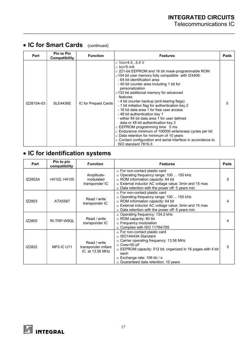
• IС for Smart Cards (continued) Part Pin to Pin
Compatibility Function Features Pads
IZ2815A-03 SLE4436E IC for Prepaid Cards
Vcc=4.5...5.5 V Icc=5 mA 221-bit EEPROM and 16 bit mask-programmable ROM 104 bit user memory fully compatible with IZ4406: - 64 bit identification area - 40 bit counter area including 1 bit for personalization 133 bit additional memory for advanced features - 4 bit counter backup (anti-tearing flags) - 1 bit initiation flag for authentication key 2 - 16 bit data area 1 for free user access - 48 bit authentication key 1 - either 64 bit data area 1 for user defined data or 48 bit authentication key 2 EEPROM programming time 5 ms Endurance minimum of 100000 write/erase cycles per bit Data retention for minimum of 10 years Contact configuration and serial interface in accordance to ISO standard 7816-3
5
• IC for identification systems Part Pin to pin
compatibility Function Features Pads
IZ2802A Н4102, H4100Amplitude-modulated
transponder IC
For non-contact plastic card Operating frequency range: 100 ... 150 kHz ROM information capacity: 64 bit External inductor AC voltage value: 3min and 15 max Data retention with the power off: 5 years min
5
IZ2803 ATA5567 Read / write transponder IC
For non-contact plastic card Operating frequency range: 100 ... 150 kHz ROM information capacity: 64 bit External inductor AC voltage value: 3min and 15 max Data retention with the power off: 5 years min
4
IZ2805 RI-TRP-W9QL Read / write transponder IC
Operating frequency: 134,2 kHz ROM capacity: 80 bit Frequency modulation Complies with ISO 11784/785
4
IZ2822 MF0 IC U11 Read / write
transponder mifare IC at 13.56 MHz
For non-contact plastic card ISO14443А Standard Carrier operating frequency: 13.56 MHz Сres=50 pF EEPROM capacity: 512 bit, organized in 16 pages with 4 bit each
Exchange rate: 106 kb / s Guaranteed data retention: 10 years
5
INTEGRATED CIRCUITS Telecommunications IC
18
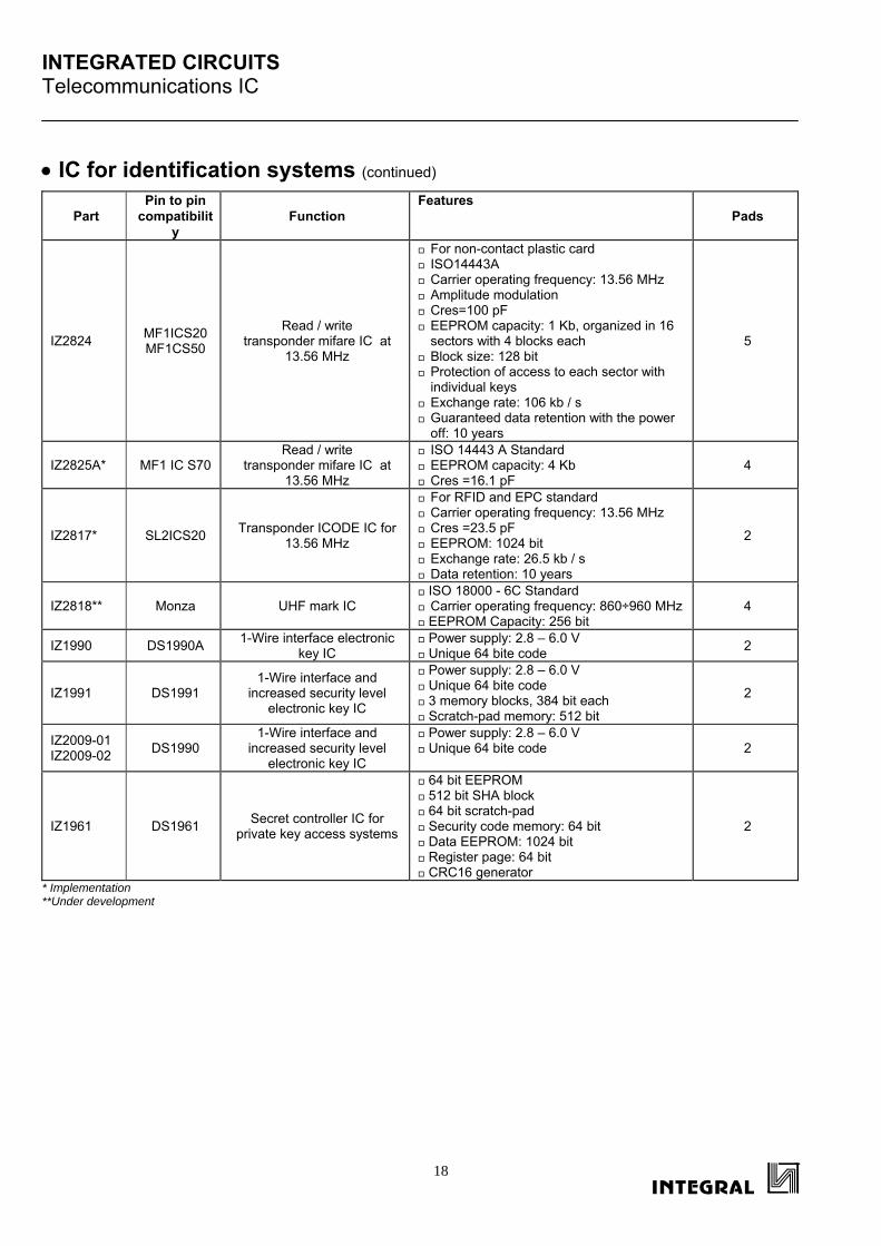
• IC for identification systems (continued)
Part Pin to pin
compatibility
Function Features
Pads
IZ2824 MF1ICS20 MF1CS50
Read / write transponder mifare IC at
13.56 MHz
For non-contact plastic card ISO14443А Carrier operating frequency: 13.56 MHz Amplitude modulation Сres=100 pF EEPROM capacity: 1 Kb, organized in 16 sectors with 4 blocks each
Block size: 128 bit Protection of access to each sector with individual keys
Exchange rate: 106 kb / s Guaranteed data retention with the power off: 10 years
5
IZ2825A* MF1 IC S70 Read / write
transponder mifare IC at 13.56 MHz
ISO 14443 A Standard EEPROM capacity: 4 Kb Сres =16.1 pF
4
IZ2817* SL2ICS20 Transponder ICODE IC for 13.56 MHz
For RFID and EPC standard Carrier operating frequency: 13.56 MHz Сres =23.5 pF EEPROM: 1024 bit Exchange rate: 26.5 kb / s Data retention: 10 years
2
IZ2818** Monza UHF mark IC ISO 18000 - 6С Standard Carrier operating frequency: 860÷960 MHz EEPROM Capacity: 256 bit
4
IZ1990 DS1990A 1-Wire interface electronic key IC
Power supply: 2.8 – 6.0 V Unique 64 bite code 2
IZ1991 DS1991 1-Wire interface and
increased security level electronic key IC
Power supply: 2.8 – 6.0 V Unique 64 bite code 3 memory blocks, 384 bit each Scratch-pad memory: 512 bit
2
IZ2009-01 IZ2009-02 DS1990
1-Wire interface and increased security level
electronic key IC
Power supply: 2.8 – 6.0 V Unique 64 bite code 2
IZ1961 DS1961 Secret controller IC for private key access systems
64 bit EEPROM 512 bit SHA block 64 bit scratch-pad Security code memory: 64 bit Data EEPROM: 1024 bit Register page: 64 bit CRC16 generator
2
* Implementation **Under development
INTEGRATED CIRCUITS Power Electronics, Standard Analog IC
19
• IC for Control and Power Electronics Part Pin to Pin
Compatibility Function Package
IL33035N IL33035DW MC33035 Brushless DC Motor Controller DIP-24
SO-24 IL33153PN MC33153P Single IGBT Gate Driver DIP-8 IL33262N IL33262D MC33262 Power Factor Controller (TA= -40...+105°C) DIP-8
SO-8 IL34262N IL34262D MC34262 Power Factor Controller DIP-8
SO-8 IL6562D L6562 SO-8 IL6562N L6562 Power Factor Controller DIP-8
IL7101N/AN/BN IL7101D/AD/BD GL7101 Earth Leakage Current Detector (UT= 4..9 mV for AN)
(UT= 9..18 mV for N/D)
DIP-8 DIP-8 SO-8
IL4145AN RV4145A Low Power Ground Fault Interrupter DIP-8 ILN2003AN ULN2003A High-Voltage High-Current Darlington Transistor Arrays DIP-16 ILN2004AN ILN2004AD ULN2004A High-Voltage High-Current Darlington Transistor Arrays DIP-16
SO-16 ILN62083N ILN62083D TD62083AFN
8CH Darlington Sink Driver
DIP-18 SO-18
ILN62084N ILN62084D TD62084AFN DIP-18
SO-18 ILN62783N ILN62783D TD62783AFN DIP-18
SO-18 ILN62784N ILN62784D TD62784AFN DIP-18
SO-18
Part Topr (°С)
IOUT (max) (mA)
VCE (max)
(V)
IIN(max) (mA)
VIN(max)
(V)
VF /VR(max) (V/V)
Designation Package
7CH High-Voltage Drivers ILN2003AN - 20 ÷ +85 500 50 1.35 30 2/50 TTL, 5V CMOS DIP-16 ILN2004AN ILN2004AD - 20 ÷ +85 500 50 1.35 30 2/50 6 ~ 15V PMOS, CMOS DIP-16
SO-16 8CH High-Voltage Drivers ILN62083N ILN62083D - 40 ÷ +85 500 50 1.35 30 2/50 TTL, 5V CMOS DIP-18
SO-18 ILN62084N ILN62084D - 40 ÷ +85 500 50 0.50 30 2/50 6 ~ 15V PMOS, CMOS DIP-18
SO-18 ILN62783N ILN62783D - 40 ÷ +85 -500 50 0.26 30 2/50 TTL, 5V CMOS DIP-18
SO-18 ILN62784N ILN62784D - 40 ÷ +85 -500 50 0.13 30 2/50 6 ~ 15V PMOS, CMOS DIP-18
SO-18
INTEGRATED CIRCUITS Power Electronics, Standard Analog IC
20
• Automotive Part Pin to Pin
Compatibility Function Package
IL33193N IL33193D MC33193
Automotive Direction Indicator RS=20 mΩ, Fn=2.2, Duty Cycle (Normal Operation) 45÷55%, Duty Cycle (One 21 W Lamp Defect) 35÷45%, Defect Lamp Detector Threshold 42.5÷56 mV, RSS=220 Ω
DIP-8 SO-8
IL33193N-03 IL33193D-03 UEA1041B
Automotive Direction Indicator RS=30 mΩ, Fn=2.5, Duty Cycle (Normal Operation) 45÷55%, Duty Cycle (One 21 W Lamp Defect) 35÷45%, Defect Lamp Detector Threshold 75÷95 mV, RSS=220 Ω, Short Circuit Detector Threshold
DIP-8 SO-8
IL33197AN IL33197AD MC33197A
Automotive Wash Wiper Timer Output Clamp Voltage (Iout=20 mА) 19.5÷22 V, Internally incorporated Zener diode 20 V
DIP-8 SO-8
IL6083N IL6083N-01 U6083B
Power Control With Interference Suppression (for N-01: Duty cycle 10… 100%, VS1=24.5…28.0 V, VS2=18.5…22.0 V, VBatt1=16.7…21.0 V (switched on), VBatt1=18.3…22.5 V (switched off), VTS=10.1…10.7 V, IS=5…17 mA)
DIP-8
IN9014N For light control relay IC DIP-8 IL8190N IL8190DW
CS8190ENF16 Precision Air-Core Tach/Speedo Driver with Return to Zero
DIP-16 SO-20 CS8190EDWF20
IL33290AD MC33290 ISO K Line Serial Link Interface SO-8 ILA82C251D PCA82C251T CAN transceiver for 24 V systems SO-8 IN2515/AN/ADW/BN/BDW MCP2515 CAN Controller SO-18 IL33091AN IL33091AD MC33091A High-Side MOS Driver DIP-8
SO-8
ILE4250GS TLE4250G Low-Drop Voltage Tracker (2÷36 V); 50 mA: Reverse Polarity Protection
P-TO-263-5-1 TO-220AB/5
ILE4260 ILE4260-2 TLE4260 Low-Drop Voltage Regulator 5 V; 500 mA; Reverse
Polarity Protection P-TO-220-5-12
ILE4264G IZE4264-2
TLE4264G TLE4264-2G
Low-Drop Voltage Regulator 5 V; 100 mA; Reverse Polarity Protection
P-SOT223-4-1 Chip
ILE4266G IZE4266-2
TLE4266G TLE4266-2G
Low-Drop Voltage Regulator 5 V; 100 mA; Reverse Polarity Protection
P-SOT223-4-2 Chip
ILE4267G ILE4267S
TLE4267G TLE4267S
Low-Drop Voltage Regulator 5 V; 400 mA; Reverse Polarity Protection
P-TO-220-7-180 P-TO-220-7-230
ILE4268GDW TLE4268G Low-Drop Voltage Regulator 5 V; 150 mA; Reverse Polarity Protection P-DSO-20-6
ILE4270G ILE4270S ILE4270Q IL4270
TLE4270G TLE4270S
Low-Drop Voltage Regulator 5 V; 550 mA; Reverse Polarity Protection IL4270 - without “RESET”
P-TO-263-5-1 P-TO-220-5-12 P-TO-220-5-11
TO-220AB/3
ILE4271G ILE4271S
TLE4271G TLE4271S
Low-Drop Voltage Regulator 5 V; 550 mA; Reverse Polarity Protection
P-TO-220-7-180 P-TO-220-7-230
ILE4274V50/V85/V10 TLE4274 Low-Drop Voltage Regulator 5 V/8.5 V/10 V; 400 mA: Reverse Polarity Protection TO-220AB/3
ILE4275G/S TLE4275G Low-Drop Voltage regulator 5 V; 400 mA: Reverse Polarity Protection
P-TO-263-5-1 TO-220AB/5
ILE4276VG/VS/V50G/V50S/V85G/V85S/V10S TLE4276 Low-Drop Voltage Regulator 5 V/8.5 V/10 V; 400 mA:
Reverse Polarity Protection P-TO-263-5-1 TO-220AB/5
IZE4278 TLE4278 Low-Drop Voltage Regulator 5 V; 150 mA: Reverse Polarity Protection Chip
IZ4206 TLE4206G 1 A DC Motor Driver for Serve Driver Applications Chip IZE4263** TLE4263 LDO Regulator 5 V; 150 mA Chip IZE4279** TLE4279 LDO Regulator 5 V; 150 mA Chip
INTEGRATED CIRCUITS Power Electronics, Standard Analog IC
21
• Timers Part Pin to Pin
Compatibility Function Package
Digital timers IN555N IN555D NE555 Timer DIP-8
SO-8 ILC555N ILC555D GLC555 Timer DIP-8
SO-8 IN556N IN556D NE556 Dual Timer DIP-14
SO-14 ILC556N GLC556 Dual Timer DIP-14 IN558N NE558 Quad Timer DIP-16 ILC558N GLC558 Quad Timer DIP-16
• Comparators Part Pin to Pin
Compatibility Function Package
IL311AN IL311AD IL311ANM
LM311, LM211 Highly Flexible Voltage Comparators (TA= -45...+85°C) DIP-8 SO-8
DIP-14 IL339N IL339D LM339 Quad Comparator DIP-14
SO-14 IL293N IL293D LM293 Dual Comparator (TA= -40...+85°C) DIP-8
SO-8 IL393N IL393D LM393 Dual Comparator DIP-8
SO-8
• Comparators (Reference Data)
Part Topr (°С)
IIB (nA) Max
Vio (mV) Max
Iio (nA) Max
Av (V/mV)
Min
Response Time (ns) Typ
Supply Voltage
(V) Package
Single Comparators
IL311ANM -45 ÷ +85 250 3.0 50 150 300 +15, -15
DIP-14 IL311AN DIP-8 IL311AD SO-8
Dual Comparators
IL293N -40 ÷ +85 250 5.0 50 50 300
±2.5 ÷ ±15 or
5.0 ÷ 30
DIP-8 IL293D SO-8 IL393N 0 ÷ +70 DIP-8 IL393D SO-8
Quad Comparators
IL339N 0 ÷ +70 250 5.0 50 200 300
±2.5 ÷ ±15 or
5.0 ÷ 30
DIP-14
IL339D SO-14
• T
imer
s (R
efer
ence
Dat
e)
CM
OS
TIM
ERS
(ILC
555N
/D, I
LC55
6N, I
LC55
8N)
BIP
OLA
R T
IMER
S (IN
55N
/D, I
N55
6N/D
, IN
558N
) Pa
ram
eter
Te
st C
ondi
tion
Valu
e U
nit
Test
Con
ditio
n Va
lue
Uni
t
Vcc
Min
Ty
pe
Max
Vc
c M
in
Type
M
ax
Su
pply
Vol
tage
, Vcc
- 2
0°C
≤ T
A ≤
+ 7
0°C
2
18
V
- 10°
C ≤
TA ≤
+ 7
0°C
4.
5
16
V Su
pply
Cur
rent
, IC
C
IL
C55
5 2 18
—
—
60
12
0 20
0 30
0 μA
IN55
5 5 15
—
—
30
00
1000
0 60
00
1500
0 μA
ILC
556
2 18
—
—
120
240
400
600
IN55
6 5 15
—
—
60
00
1600
0 12
000
3000
0 IL
C55
8 2 18
—
—
24
0 48
0 80
0 12
00
IN55
8 15
—
16
000
36
000
Tim
ing
Erro
r R
=1–
100
kΩ,
C =
0.1
μF
R
=1–
100k
Ω,
C =
0.1μF
Initi
al A
ccur
acy,
t A
2.
0 5.
0 %
2.
25
%
D
rift W
ith T
empe
ratu
re,
ΔtA
/ΔT
5 10
15
50
200
300
600
ppm
/°C
150
pp
m /°C
D
rift W
ith S
uppl
y Vo
ltage
, Δ
tA/Δ
Vs
5 1.
0 3.
0 %
/ V
0.3
%
/ V
Thre
shol
d Vo
ltage
, VTH
5 0.
65xV
cc0.
67xV
cc
0.7x
Vcc
V
5 15
3.
33
10
V
Trig
ger V
olta
ge, V
TRIG
5 0.
31xV
cc0.
33xV
cc
0.36
xVcc
V
5 15
1.
1 4.
5 1.
67
5.0
2.2
5.6
V
Trig
ger C
urre
nt, I
TRIG
18
5 2
50
10
1.0
pA
V TR
IG =
0V
0.5
2.0
µA
Thre
shol
d C
urre
nt, I
TH
18
5 2
50
10
1.0
pA
0.
1 0.
25
µA
Res
et C
urre
nt, I
RST
V R
ESET
= G
roun
d 18
5 2
100
20
2.0
pA
V RES
ET =
0V
0.1
0.4
mA
Res
et V
olta
ge, V
RST
18
2 0.
4 0.
4 0.
7 0.
7 1.
0 1.
0 V
0.4
0.7
1.0
V
Con
trol
Vol
tage
Lea
d, V
CV
0.65
xVcc
0.67
xVcc
0.
69xV
cc
V
15
5 9.
0 2.
6 10
3.
33
11
4.0
V
Out
put V
olta
ge L
ow, V
OL
I O =
20
mA
I O
= 3
.2 m
A
15
5
0.4
0.2
1.0
0.4
V I O
= 1
0mA
I O
= 5
0mA
I O
= 8
mA
I O
= 5
mA
15
15
5 5
0.
1 0.
4 0.
3 0.
25
0.25
0.
75
0.4
0.35
V
Out
put V
olta
ge H
igh,
VO
H
I O =
0.8
mA
I O
= 0
.8 m
A
15
5 14
.3
4.0
14.6
4.
3
V I O
= 1
00m
A
I O =
200
mA
I O
= 1
00m
A
15
15
5
12.7
5 2.
75
13.3
12
.5
3.3
V
Ris
e (F
all)
Tim
e of
Out
put,
t TLH
, t TH
L R
L =
10 М
Ω,
СL =
10
pF
5 35
40
75
ns
100
ns
Gua
rant
eed
Max
Osc
Fre
q,
fmax
A
stab
le O
pera
tion
50
0
kH
z
50
0
kH
z
Ope
ratin
g Te
mpe
ratu
re, T
opr
- 20
to +
70
ºC
- 10
to +
70
ºC
Not
e:
T A =
25°
C, V
cc =
+ 2
– +
15V
unl
ess
othe
r spe
cifie
d T A
= 2
5°C
, Vcc
= +
5 –
+ 1
5V u
nles
s ot
her s
peci
fied
INTEGRATED CIRCUITS Power Electronics, Standard Analog IC
22
INTEGRATED CIRCUITS Power Electronics, Standard Analog IC
23
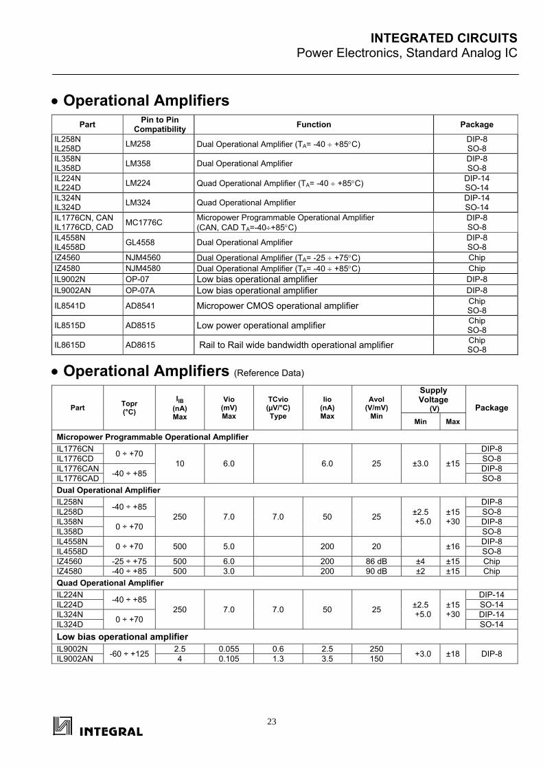
• Operational Amplifiers Part Pin to Pin
Compatibility Function Package
IL258N IL258D LM258 Dual Operational Amplifier (TA= -40 ÷ +85°C) DIP-8
SO-8 IL358N IL358D LM358 Dual Operational Amplifier DIP-8
SO-8 IL224N IL224D LM224 Quad Operational Amplifier (TA= -40 ÷ +85°C) DIP-14
SO-14 IL324N IL324D LM324 Quad Operational Amplifier DIP-14
SO-14 IL1776CN, CAN IL1776CD, CAD MC1776C Micropower Programmable Operational Amplifier
(CAN, CAD TA=-40÷+85°C) DIP-8 SO-8
IL4558N IL4558D GL4558 Dual Operational Amplifier DIP-8
SO-8 IZ4560 NJM4560 Dual Operational Amplifier (TA= -25 ÷ +75°C) Chip IZ4580 NJM4580 Dual Operational Amplifier (TA= -40 ÷ +85°C) Chip IL9002N OP-07 Low bias оperational аmplifier DIP-8 IL9002AN OP-07A Low bias оperational аmplifier DIP-8
IL8541D AD8541 Micropower CMOS operational amplifier Chip SO-8
IL8515D AD8515 Low power operational amplifier Chip SO-8
IL8615D AD8615 Rail to Rail wide bandwidth operational amplifier Chip SO-8
• Operational Amplifiers (Reference Data)
Part Topr (°С)
IIB (nA) Max
Vio (mV) Max
TСvio (µV/°C) Type
Iio (nA) Max
Avol (V/mV)
Min
Supply Voltage
(V) Package Min Max
Micropower Programmable Operational Amplifier IL1776CN 0 ÷ +70
10 6.0 6.0 25 ±3.0 ±15
DIP-8 IL1776CD SO-8 IL1776CAN -40 ÷ +85 DIP-8 IL1776CAD SO-8 Dual Operational Amplifier IL258N -40 ÷ +85
250 7.0 7.0 50 25 ±2.5 +5.0
±15 +30
DIP-8 IL258D SO-8 IL358N 0 ÷ +70 DIP-8 IL358D SO-8 IL4558N 0 ÷ +70 500 5.0 200 20 ±16 DIP-8 IL4558D SO-8 IZ4560 -25 ÷ +75 500 6.0 200 86 dB ±4 ±15 Chip IZ4580 -40 ÷ +85 500 3.0 200 90 dB ±2 ±15 Chip Quad Operational Amplifier IL224N -40 ÷ +85
250 7.0 7.0 50 25 ±2.5 +5.0
±15 +30
DIP-14 IL224D SO-14 IL324N 0 ÷ +70 DIP-14 IL324D SO-14 Low bias оperational аmplifier IL9002N -60 ÷ +125 2.5 0.055 0.6 2.5 250 +3.0 ±18 DIP-8 IL9002AN 4 0.105 1.3 3.5 150
INTEGRATED CIRCUITS Power Electronics, Standard Analog IC
24
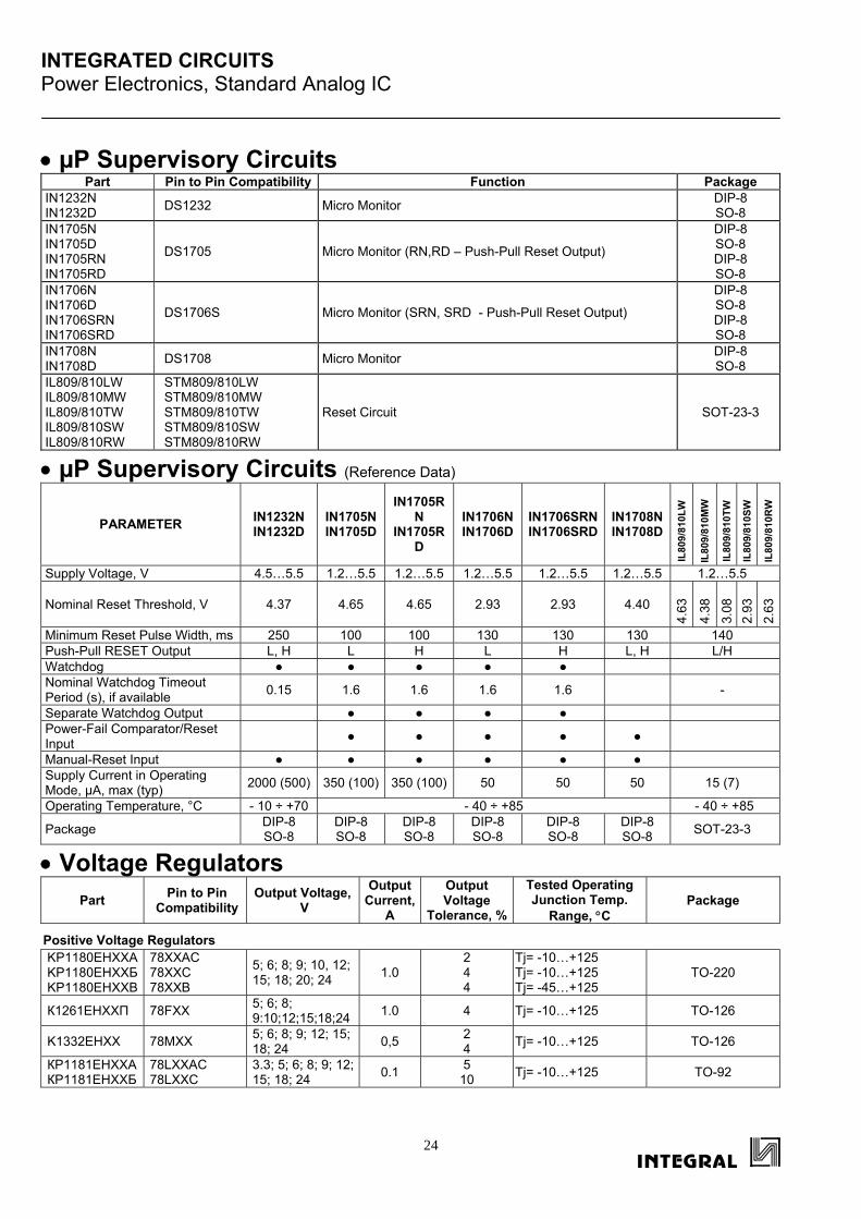
• µP Supervisory Circuits Part Pin to Pin Compatibility Function Package
IN1232N IN1232D DS1232 Micro Monitor DIP-8
SO-8 IN1705N IN1705D IN1705RN IN1705RD
DS1705 Micro Monitor (RN,RD – Push-Pull Reset Output)
DIP-8 SO-8 DIP-8 SO-8
IN1706N IN1706D IN1706SRN IN1706SRD
DS1706S Micro Monitor (SRN, SRD - Push-Pull Reset Output)
DIP-8 SO-8 DIP-8 SO-8
IN1708N IN1708D DS1708 Micro Monitor DIP-8
SO-8 IL809/810LW IL809/810MW IL809/810TW IL809/810SW IL809/810RW
STM809/810LW STM809/810MW STM809/810TW STM809/810SW STM809/810RW
Reset Circuit SOT-23-3
• µP Supervisory Circuits (Reference Data)
PARAMETER IN1232N IN1232D
IN1705NIN1705D
IN1705RN
IN1705RD
IN1706NIN1706D
IN1706SRNIN1706SRD
IN1708N IN1708D
IL80
9/81
0LW
IL80
9/81
0MW
IL80
9/81
0TW
IL80
9/81
0SW
IL80
9/81
0RW
Supply Voltage, V 4.5…5.5 1.2…5.5 1.2…5.5 1.2…5.5 1.2…5.5 1.2…5.5 1.2…5.5
Nominal Reset Threshold, V 4.37 4.65 4.65 2.93 2.93 4.40
4.63
4.38
3.08
2.
93
2.63
Minimum Reset Pulse Width, ms 250 100 100 130 130 130 140 Push-Pull RESET Output L, H L H L H L, H L/H Watchdog ● ● ● ● ● Nominal Watchdog Timeout Period (s), if available 0.15 1.6 1.6 1.6 1.6 -
Separate Watchdog Output ● ● ● ● Power-Fail Comparator/Reset Input ● ● ● ● ●
Manual-Reset Input ● ● ● ● ● ● Supply Current in Operating Mode, µA, max (typ) 2000 (500) 350 (100) 350 (100) 50 50 50 15 (7)
Operating Temperature, °C - 10 ÷ +70 - 40 ÷ +85 - 40 ÷ +85
Package DIP-8 SO-8
DIP-8 SO-8
DIP-8 SO-8
DIP-8 SO-8
DIP-8 SO-8
DIP-8 SO-8 SOT-23-3
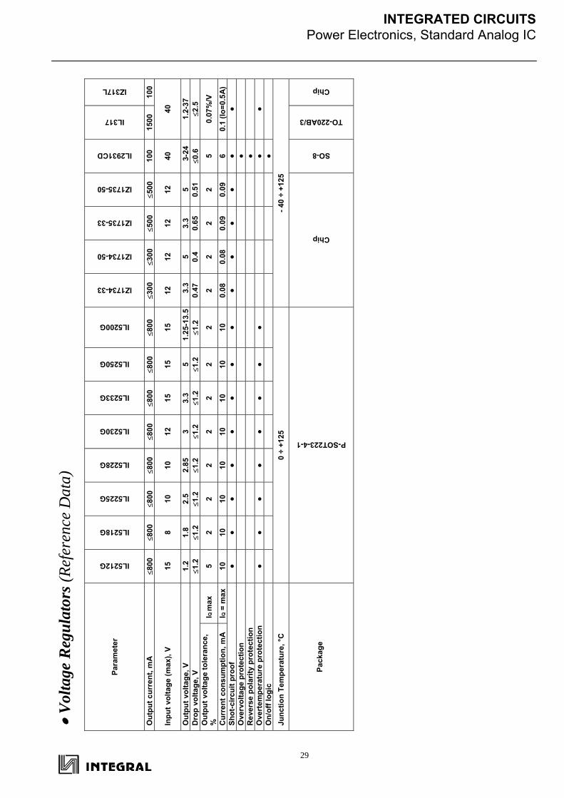
• Voltage Regulators Part Pin to Pin
Compatibility Output Voltage,
V Output
Current,A
Output Voltage
Tolerance, %
Tested Operating Junction Temp.
Range, °C Package
Positive Voltage Regulators KP1180EHXXA KP1180EHXXБ KP1180EHXXВ
78XXAC 78XXC 78XXB
5; 6; 8; 9; 10, 12; 15; 18; 20; 24 1.0
2 4 4
Tj= -10…+125 Tj= -10…+125 Tj= -45…+125
TO-220
К1261ЕНХХП 78FXX 5; 6; 8; 9:10;12;15;18;24 1.0 4 Tj= -10…+125 TO-126
K1332EHXX 78MXX 5; 6; 8; 9; 12; 15; 18; 24 0,5 2
4 Tj= -10…+125 TO-126
КР1181ЕНХХА КР1181ЕНХХБ
78LXXAC 78LXXC
3.3; 5; 6; 8; 9; 12; 15; 18; 24 0.1 5
10 Tj= -10…+125 TO-92
INTEGRATED CIRCUITS Power Electronics, Standard Analog IC
25
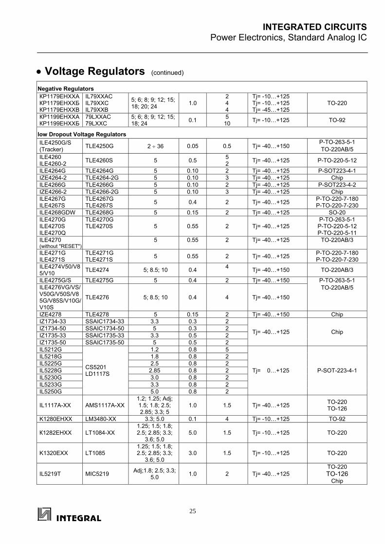
• Voltage Regulators (continued)
Negative Regulators КР1179ЕНХХА КР1179ЕНХХБ КР1179ЕНХХВ
IL79XXAC IL79XXC IL79XXB
5; 6; 8; 9; 12; 15; 18; 20; 24 1.0
2 4 4
Tj= -10…+125 Tj= -10…+125 Tj= -45…+125
TO-220
КР1199ЕНХХА КР1199ЕНХХБ
79LXXAC 79LXXC
5; 6; 8; 9; 12; 15; 18; 24 0.1 5
10 Tj= -10…+125 TO-92
low Dropout Voltage Regulators ILE4250G/S (Tracker) TLE4250G 2 ÷ 36 0.05 0.5 Tj= -40…+150
P-TO-263-5-1 TO-220AB/5
ILE4260 ILE4260-2 TLE4260S 5 0.5 5
2 Tj= -40…+125 P-TO-220-5-12
ILE4264G TLE4264G 5 0.10 2 Tj= -40…+125 P-SOT223-4-1 IZE4264-2 TLE4264-2G 5 0.10 3 Tj= -40…+125 Chip ILE4266G TLE4266G 5 0.10 2 Tj= -40…+125 P-SOT223-4-2 IZE4266-2 TLE4266-2G 5 0.10 3 Tj= -40…+125 Chip ILE4267G ILE4267S
TLE4267G TLE4267S 5 0.4 2 Tj= -40…+125 P-TO-220-7-180
P-TO-220-7-230 ILE4268GDW TLE4268G 5 0.15 2 Tj= -40…+125 SO-20 ILE4270G ILE4270S ILE4270Q
TLE4270G TLE4270S
5 0.55 2 Tj= -40…+125 P-TO-263-5-1
P-TO-220-5-12 P-TO-220-5-11
ILE4270 (without "RESET")
5 0.55 2 Tj= -40…+125 TO-220AB/3
ILE4271G ILE4271S
TLE4271G TLE4271S 5 0.55 2 Tj= -40…+125 P-TO-220-7-180
P-TO-220-7-230 ILE4274V50/V85/V10 TLE4274 5; 8.5; 10 0.4 4 Tj= -40…+150 TO-220AB/3
ILE4275G/S TLE4275G 5 0.4 2 Tj= -40…+150 P-TO-263-5-1 TO-220AB/5 ILE4276VG/VS/
V50G/V50S/V85G/V85S/V10G/V10S
TLE4276 5; 8.5; 10 0.4 4 Tj= -40…+150
IZE4278 TLE4278 5 0.15 2 Tj= -40…+150 Chip IZ1734-33 SSAIC1734-33 3.3 0.3 2
Tj= -40…+125 Chip IZ1734-50 SSAIC1734-50 5 0.3 2 IZ1735-33 SSAIC1735-33 3.3 0.5 2 IZ1735-50 SSAIC1735-50 5 0.5 2 IL5212G
CS5201 LD1117S
1.2 0.8 5
Tj= 0…+125 P-SOT-223-4-1
IL5218G 1.8 0.8 2 IL5225G 2.5 0.8 2 IL5228G 2.85 0.8 2 IL5230G 3.0 0.8 2 IL5233G 3.3 0.8 2 IL5250G 5.0 0.8 2
IL1117A-XX AMS1117A-XX 1.2; 1.25; Adj; 1.5; 1.8; 2.5; 2.85; 3.3; 5
1.0 1.5 Tj= -40…+125 TO-220 TO-126
K1280EHXX LM3480-XX 3.3; 5.0 0.1 4 Tj= -10…+125 TO-92
К1282ЕНХХ LT1084-XХ 1.25; 1.5; 1.8; 2.5; 2.85; 3.3;
3.6; 5.0 5.0 1.5 Tj= -10…+125 TO-220
K1320EXX LT1085 1.25; 1.5; 1.8; 2.5; 2.85; 3.3;
3.6; 5.0 3.0 1.5 Tj= -10…+125 TO-220
IL5219T MIC5219 Adj;1.8; 2.5; 3.3; 5.0 1.0 2 Tj= -40…+125
TO-220 TO-126
Chip
INTEGRATED CIRCUITS Power Electronics, Standard Analog IC
26
• Voltage Regulators (continued)
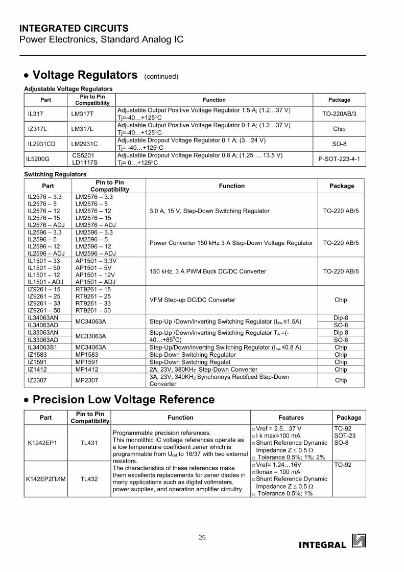
Adjustable Voltage Regulators
Part Pin to Pin Compatibility Function Package
IL317 LM317T Adjustable Output Positive Voltage Regulator 1.5 A; (1.2…37 V) Tj=-40…+125°C TO-220AB/3
IZ317L LM317L Adjustable Output Positive Voltage Regulator 0.1 A; (1.2…37 V) Tj=-40…+125°C Chip
IL2931CD LM2931C Adjustable Dropout Voltage Regulator 0.1 A; (3…24 V) Tj= -40…+125°C SO-8
IL5200G CS5201 LD1117S
Adjustable Dropout Voltage Regulator 0.8 А; (1.25 … 13.5 V) Tj= 0…+125°C P-SOT-223-4-1
Switching Regulators
Part Pin to Pin Compatibility Function Package
IL2576 – 3.3 IL2576 – 5 IL2576 – 12 IL2576 – 15 IL2576 – ADJ
LM2576 – 3.3 LM2576 – 5 LM2576 – 12 LM2576 – 15 LM2576 – ADJ
3.0 A, 15 V, Step-Down Switching Regulator TO-220 AB/5
IL2596 – 3.3 IL2596 – 5 IL2596 – 12 IL2596 – ADJ
LM2596 – 3.3 LM2596 – 5 LM2596 – 12 LM2596 – ADJ
Power Converter 150 kHz 3 A Step-Down Voltage Regulator TO-220 AB/5
IL1501 – 33 IL1501 – 50 IL1501 – 12 IL1501 - ADJ
AP1501 – 3.3V AP1501 – 5V AP1501 – 12V AP1501 – ADJ
150 kHz, 3 A PWM Buck DC/DC Converter TO-220 AB/5
IZ9261 – 15 IZ9261 – 25 IZ9261 – 33 IZ9261 – 50
RT9261 – 15 RT9261 – 25 RT9261 – 33 RT9261 – 50
VFM Step-up DC/DC Converter Chip
IL34063AN MC34063A Step-Up /Down/inverting Switching Regulator (Isw ≤1.5A) Dip-8 IL34063AD SO-8 IL33063AN MC33063A Step-Up /Down/inverting Switching Regulator TA =(-
40…+850C) Dip-8
IL33063AD SO-8 IL34063S1 MC34063A Step-Up/Down/inverting Switching Regulator (Isw ≤0.8 A) Chip IZ1583 MP1583 Step-Down Switching Regulator Chip IZ1591 MP1591 Step-Down Switching Regulat Chip IZ1412 MP1412 2A, 23V, 380KHZ Step-Down Converter Chip
IZ2307 MP2307 3A, 23V, 340KHZ Synchonoys Rectifced Step-Down Converter Chip
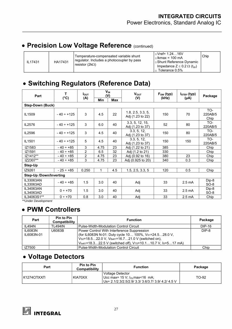
• Precision Low Voltage Reference Part Pin to Pin
Compatibility Function Features Package
K1242EP1 TL431 Programmable precision references. This monolithic IC voltage references operate as a low temperature coefficient zener which is programmable from Uref to 16/37 with two external resistors. The characteristics of these references make them excellents replacements for zener diodes in many applications such as digital voltmeters, power supplies, and operation amplifier circultry.
Vref = 2.5…37 V I k max=100 mA Shunt Reference Dynamic Impedance Z ≤ 0.5 Ω Tolerance 0.5%; 1%; 2%
TO-92 SOT-23 SO-8
K142EP2ПИМ TL432
Vref= 1.24…16V Ikmax = 100 mA Shunt Reference Dynamic Impedance Z ≤ 0.5 Ω Tolerance 0.5%; 1%
TO-92
INTEGRATED CIRCUITS Power Electronics, Standard Analog IC
27
• Precision Low Voltage Reference (continued)
IL17431 HA17431
Temperature-compensated variable shunt regulator. Includes a photocoupler by pass resistor (2kΩ)
Vref= 1.24…16V Ikmax = 100 mA Shunt Reference Dynamic Impedance Z ≤ 0.2 Ω (typ) Tolerance 0.5%
Chip
• Switching Regulators (Reference Data)
Part T (°С)
IOUT (A)
ViN(V) VOUT
(V) FSW (typ)
(kHz) ISTBY (typ)
(µA) Package Min Max
Step-Down (Buck)
IL1509 - 40 ÷ +125 3 4.5 22 1.8, 2.5, 3.3, 5, Adj (1.23 to 22) 150 70
TO-220AB/5
Chip
IL2576 - 40 ÷ +125 3 6.0 40 3.3, 5, 12, 15, Adj (1.23 to 37) 52 80 TO-
220AB/5
IL2596 - 40 ÷ +125 3 4.5 40 3.3, 5, 12, Adj (1.23 to 37) 150 80 TO-
220AB/5
IL1501 - 40 ÷ +125 5 4.5 40 3.3, 5, 12, Adj (1.23 to 37) 150 150 TO-
220AB/5 IZ1583 - 40 ÷ +85 3 4.75 23 Adj (1.22 to 21) 385 Chip IZ1591 - 40 ÷ +85 2 6.5 32 Adj (1.2 to 21) 330 Chip IZ1412** - 40 ÷ +85 2 4.75 23 Adj (0.92 to 16) 380 23 Chip IZ2307** - 40 ÷ +85 3 4.75 23 Adj (0.925 to 20) 340 0.3 Chip Step-Up IZ9261 - 25 ÷ +85 0.250 1 4.5 1.5, 2.5, 3.3, 5 120 0.5 Chip Step-Up /Down/Inverting IL33063AN IL33063AD - 40 ÷ +85 1.5 3.0 40 Adj 33 2.5 mA Dip-8
SO-8 IL34063AN IL34063AD 0 ÷ +70 1.5 3.0 40 Adj 33 2.5 mA Dip-8
SO-8 IL34063S1** 0 ÷ +70 0.8 3.0 40 Adj 33 2.5 mA Chip
**Under Development
• PWM Controllers Part Pin to Pin
Compatibility Function Package
IL494N TL494IN Pulse-Width-Modulation Control Circuit DIP-16 IL6083N IL6083N-01
U6083B Power Control With Interference Suppression (for IL6083N N-01: Duty cycle 10… 100%, VS1=24.5…28.0 V, VS2=18.5…22.0 V, VBatt1=16.7…21.0 V (switched on), Vbatt1=18.3…22.5 V (switched off), VTS=10.1…10.7 V, IS=5…17 mA)
DIP-8
IZ7500 Pulse-Width-Modulation Control Circuit Chip
• Voltage Detectors Part Pin to Pin
Compatibility Function Package
К1274СПХХП KIA70ХХ Voltage Detector Ucc max= 15 V; IOLmax<16 mA; Us= 2.1/2.3/2.5/2.9/ 3.3/ 3.6/3.7/ 3.9/ 4.2/ 4.5 V
TO-92

• V
olta
ge R
egul
ator
s (Re
fere
nce
Dat
a)
Para
met
er
ILE4250G/S (Tracker)
ILE4260
ILE4260-2
ILE4264G
IZE4264-2
ILE4266G
IZE4266-2
ILE4267G/S
ILE4268GDW
ILE4270G/S/Q
IL4270
ILE4271G/S
ILE4274V50/V85/V10
ILE4275G/S
ILE4276VG/VS/V50G/V50S/V85G/V85S/V10G/V
10S
IZE4278
Out
put c
urre
nt, m
A
≤50
≤500
≤1
00≤1
00
≤100
≤1
00
≤400
≤1
50
≤550
≤5
50
≤400
≤4
00
≤400
≤1
50
Inpu
t vol
tage
(max
), V
45
42
60
(≤40
0ms)
45
45
45
45
42
60
(≤
400m
s)
45
42
65
(≤40
0ms)
42
65
(≤40
0ms)
45
45
45
45
Out
put v
olta
ge, V
2÷
36
5 5
5 5
5 5
5 5
5 5;
8.5
; 10
5
5; 8
.5;
10
5
Dro
p vo
ltage
, V
≤0.3
≤0
.5
≤0.5
≤0
.5
≤0.5
≤0
.5
≤0.6
≤0
.5
≤0.7
≤0
.7
≤0.5
≤0
.5≤0
.5≤0
.5
Out
put v
olta
ge
tole
ranc
e, %
I Q
max
0.
5 5
2 2
3 2
3 2
2 2
2 4
2 4
2 IQ
= 5
0 m
A
2
2
Cur
rent
con
sum
ptio
n,
mA
IQ =
max
≤65
≤15
≤1
5
≤60
≤20
≤75
≤75
≤30
≤22
≤25
≤12
IQ =
0.1
mA
≤0.0
7
≤0.0
7
IQ =
1 m
A
0.15
0.
4 -
0.22
0.
20
0.22
IQ
≤ 3
0 m
A
≤3
IQ
= 5
0 m
A
≤4
≤4
Shot
-circ
uit p
roof
●
● ●
● ●
● ●
● ●
● ●
● ●
● ●
Ove
rvol
tage
pro
tect
ion
●
●
● ●
●
R
ever
se p
olar
ity p
rote
ctio
n ●
● ●
● ●
● ●
● ●
● ●
● ●
● ●
Ove
rtem
pera
ture
pro
tect
ion
● ●
● ●
● ●
● ●
● ●
● ●
● ●
●
Adj
usta
ble
Res
et
Tim
e
●
●
● ●
●
●
●
Thre
shol
d
●
●
● ●
●
●
●
On/
off l
ogic
●
Wat
chdo
g
●
●
●
Inhi
bit I
nput
●
● ●
●
●
Junc
tion
Tem
pera
ture
, °С
- 4
0 ÷
+150
- 40
÷ +1
25
- 40
÷ +1
50
- 40
÷ +1
25
Pack
age
P-TO-263-5-1 TO-220AB/5
TO-220AB/5
P-SOT223-4-1
Chip
P-SOT223-4-2
Chip
P-TO-220-7-180 P-TO-220-7-230
SO-20
P-TO-263-5-1 P-TO-220-5-12 P-TO-220-5-11
TO-220AB/3
P-TO-220-7-180 P-TO-220-7-230
TO-220AB/3
P-TO-263-5-1 TO-220AB/5
P-TO-263-5-1 TO-220AB/5
Chip
INTEGRATED CIRCUITS Power Electronics, Standard Analog IC
28
• V
olta
ge R
egul
ator
s (Re
fere
nce
Dat
a)
Para
met
er
IL5212G
IL5218G
IL5225G
IL5228G
IL5230G
IL5233G
IL5250G
IL5200G
IZ1734-33
IZ1734-50
IZ1735-33
IZ1735-50
IL2931СD
IL317
IZ317L
Out
put c
urre
nt, m
A
≤800
≤8
00
≤800
≤8
00
≤800
≤8
00
≤800
≤8
00
≤300
≤3
00
≤500
≤5
00
100
1500
10
0
Inpu
t vol
tage
(max
), V
15
8 10
10
12
15
15
15
12
12
12
12
40
40
Out
put v
olta
ge, V
1.
2 1.
8 2.
5 2.
85
3 3.
3 5
1.25
-13.
5 3.
3 5
3.3
5 3-
24
1.2-
37
Dro
p vo
ltage
, V
≤1.2
≤1
.2
≤1.2
≤1
.2
≤1.2
≤1
.2
≤1.2
≤1
.2
0.47
0.
4 0.
65
0.51
≤0
.6
≤2.5
O
utpu
t vol
tage
tole
ranc
e,
%
IQ m
ax
5 2
2 2
2 2
2 2
2 2
2 2
5 0.
07%
/V
Cur
rent
con
sum
ptio
n, m
A
IQ =
max
10
10
10
10
10
10
10
10
0.
08
0.08
0.
09
0.09
6
0.1
(Io=0
.5А
) Sh
ot-c
ircui
t pro
of
● ●
● ●
● ●
● ●
● ●
● ●
● ●
Ove
rvol
tage
pro
tect
ion
●
Rev
erse
pol
arity
pro
tect
ion
●
Ove
rtem
pera
ture
pro
tect
ion
● ●
● ●
● ●
● ●
● ●
On/
off l
ogic
●
Ju
nctio
n Te
mpe
ratu
re, °С
0
÷ +1
25
- 40
÷ +1
25
Pa
ckag
e
P-SOT223-4-1
Chip
SO-8
ТО-220АВ/3
Chip
INTEGRATED CIRCUITSPower Electronics, Standard Analog IC
29
INTEGRATED CIRCUITS Power Electronics, Standard Analog IC, Standard Digital Logic IC
30
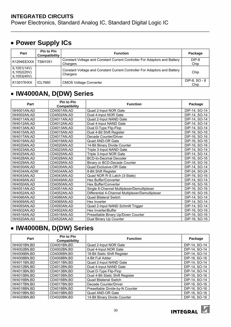
• Power Supply ICs Part Pin to Pin
Compatibility Function Package
K1294EEXXX TSM1051 Constant Voltage and Constant Current Controller For Adaptors and Battery Chargers
DIP-8 Chip
IL1051(14V) IL1052(20V) IL1053(40V)
Constant Voltage and Constant Current Controller For Adaptors and Battery Chargers Chip
K1301ПНXX ICL7660 CMOS Voltage Converter DIP-8, SO - 8 Chip
• IW4000AN, D(DW) Series Part Pin to Pin
Compatibility Function Package
IW4001AN,AD CD4001AN,AD Quad 2-Input NOR Gate DIP-14, SO-14IW4002AN,AD CD4002AN,AD Dual 4-Input NOR Gate DIP-14, SO-14IW4011AN,AD CD4011AN,AD Quad 2-Input NAND Gate DIP-14, SO-14IW4012AN,AD CD4012AN,AD Dual 4-Input NAND Gate DIP-14, SO-14IW4013AN,AD CD4013AN,AD Dual D-Type Flip-Flop DIP-14, SO-14IW4015AN,AD CD4015AN,AD Dual 4-Bit Shift Register DIP-16, SO-16IW4017AN,AD CD4017AN,AD Decade Counter/Driver DIP-16, SO-16IW4019AN,AD CD4019AN,AD Quad AND-OR Gate DIP-16, SO-16IW4020AN,AD CD4020AN,AD 14-Bit Binary Divide Counter DIP-16, SO-16IW4023AN,AD CD4023AN,AD Triple 3-Input NAND Gate DIP-14, SO-14IW4025AN,AD CD4025AN,AD Triple 3-Input NOR Gate DIP-14, SO-14IW4028AN,AD CD4028AN,AD BCD-to-Decimal Decoder DIP-16, SO-16IW4029AN,AD CD4029AN,AD Binary or BCD-Decade Counter DIP-16, SO-16IW4030AN,AD CD4030AN,AD Quad Exclusive-OR Gate DIP-14, SO-14IW4034AN,ADW CD4034AN,AD 8-Bit Shift Register DIP-24, SO-24IW4043AN,AD CD4043AN,AD Quad NOR R-S Latch (3-State) DIP-16, SO-16IW4049AN,AD CD4049AN,AD Hex Buffer/Converter DIP-14, SO-14IW4050AN,AD CD4050AN,AD Hex Buffer/Converter DIP-16, SO-16IW4051AN,AD CD4051AN,AD Single 8-Channel Multiplexer/Demultiplexer DIP-16, SO-16IW4052AN,AD CD4052AN,AD Differential 4-Channel Multiplexer/Demultiplexer DIP-16, SO-16IW4066AN,AD CD4066AN,AD Quad Bilateral Switch DIP-14, SO-14IW4069AN,AD CD4069AN,AD Hex Inverter DIP-14, SO-14IW4093AN,AD CD4093AN,AD Quad 2-Input NAND Schmitt Trigger DIP-14, SO-14IW4502AN,AD CD4502AN,AD Hex Inverter/Buffer DIP-16, SO-16IW4516AN,AD CD4516AN,AD Presettable Binary Up/Down Counter DIP-16, SO-16IW4520AN,AD CD4520AN,AD Dual Binary Up Counter DIP-16, SO-16
• IW4000BN, D(DW) Series Part Pin to Pin
Compatibility Function Package
IW4001BN,BD CD4001BN,BD Quad 2-Input NOR Gate DIP-14, SO-14 IW4002BN,BD CD4002BN,BD Dual 4-Input NOR Gate DIP-14, SO-14 IW4006BN,BD CD4006BN,BD 18-Bit Static Shift Register DIP-14, SO-14 IW4008BN,BD CD4008BN,BD 4-Bit Full Adder DIP-16, SO-16 IW4011BN,BD CD4011BN,BD Quad 2-Input NAND Gate DIP-14, SO-14 IW4012BN,BD CD4012BN,BD Dual 4-Input NAND Gate DIP-14, SO-14 IW4013BN,BD CD4013BN,BD Dual D-Type Flip-Flop DIP-14, SO-14 IW4015BN,BD CD4015BN,BD Dual 4-Bit Static Shift Register DIP-16, SO-16 IW4016BN,BD CD4016BN,BD Quad Bilaterial Switch DIP-14, SO-14 IW4017BN,BD CD4017BN,BD Decade Counter/Driver DIP-16, SO-16 IW4018BN,BD CD4018BN,BD Presettable Divide-by-N Counter DIP-16, SO-16 IW4019BN,BD CD4019BN,BD Quad AND-OR Gate DIP-16, SO-16 IW4020BN,BD CD4020BN,BD 14-Bit Binary Divide Counter DIP-16, SO-16
INTEGRATED CIRCUITS Standard Digital Logic IC
31
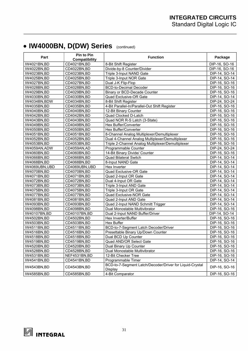
• IW4000BN, D(DW) Series (continued)
Part Pin to Pin Compatibility Function Package
IW4021BN,BD CD4021BN,BD 8-Bit Shift Register DIP-16, SO-16 IW4022BN,BD CD4022BN,BD Divide-by-8 Counter/Divider DIP-16, SO-16 IW4023BN,BD CD4023BN,BD Triple 3-Input NAND Gate DIP-14, SO-14IW4025BN,BD CD4025BN,BD Triple 3-Input NOR Gate DIP-14, SO-14IW4027BN,BD CD4027BN,BD Dual J-K Flip-Flop DIP-16, SO-16IW4028BN,BD CD4028BN,BD BCD-to-Decimal Decoder DIP-16, SO-16IW4029BN,BD CD4029BN,BD Binary or BCD-Decade Counter DIP-16, SO-16IW4030BN,BD CD4030BN,BD Quad Exclusive-OR Gate DIP-14, SO-14IW4034BN,BDW CD4034BN,BD 8-Bit Shift Register DIP-24, SO-24IW4035BN,BD CD4035BN,BD 4-Bit Parallel-In/Parallel-Out Shift Register DIP-16, SO-16IW4040BN,BD CD4040BN,BD 12-Bit Binary Counter DIP-16, SO-16IW4042BN,BD CD4042BN,BD Quad Clocked D-Latch DIP-16, SO-16IW4043BN,BD CD4043BN,BD Quad NOR R-S Latch (3-State) DIP-16, SO-16IW4049BN,BD CD4049BN,BD Hex Buffer/Converter DIP-16, SO-16IW4050BN,BD CD4050BN,BD Hex Buffer/Converter DIP-16, SO-16IW4051BN,BD CD4051BN,BD 8-Channel Analog Multiplexer/Demultiplexer DIP-16, SO-16IW4052BN,BD CD4052BN,BD Dual 4-Channel Analog Multiplexer/Demultiplexer DIP-16, SO-16IW4053BN,BD CD4053BN,BD Triple 2-Channel Analog Multiplexer/Demultiplexer DIP-16, SO-16IW4059AN,ADW CD4059AN,AD Programmable Counter DIP-24, SO-24IW4060BN,BD CD4060BN,BD 14-Bit Binary Divide/ Counter DIP-16, SO-16IW4066BN,BD CD4066BN,BD Quad Bilateral Switch DIP-14, SO-14IW4068BN,BD CD4068BN,BD 8-Input NAND Gate DIP-14, SO-14IW4069UBN,UBD CD4069UBN,UBD Hex Inverter DIP-14, SO-14IW4070BN,BD CD4070BN,BD Quad Exclusive-OR Gate DIP-14, SO-14IW4071BN,BD CD4071BN,BD Quad 2-Input OR Gate DIP-14, SO-14IW4072BN,BD CD4072BN,BD Dual 4-Input OR Gate DIP-14, SO-14IW4073BN,BD CD4073BN,BD Triple 3-Input AND Gate DIP-14, SO-14IW4075BN,BD CD4075BN,BD Triple 3-Input OR Gate DIP-14, SO-14IW4077BN,BD CD4077BN,BD Quad Exclusive-NOR Gate DIP-14, SO-14IW4081BN,BD CD4081BN,BD Quad 2-Input AND Gate DIP-14, SO-14IW4093BN,BD CD4093BN,BD Quad 2-Input NAND Schmitt Trigger DIP-14, SO-14IW4098BN,BD CD4098BN,BD Dual Monostable Multivibrator DIP-16, SO-16IW40107BN,BD CD40107BN,BD Dual 2-Input NAND Buffer/Driver DIP-14, SO-14 IW4502BN,BD CD4502BN,BD Hex Inverter/Buffer DIP-16, SO-16IW4503BN,BD CD4503BN,BD Hex Buffer DIP-16, SO-16IW4511BN,BD CD4511BN,BD BCD-to-7-Segment Latch Decoder/Driver DIP-16, SO-16IW4516BN,BD CD4516BN,BD Presettable Binary Up/Down Counter DIP-16, SO-16IW4518BN,BD CD4518BN,BD Dual BCD Up Counter DIP-16, SO-16IW4519BN,BD CD4519BN,BD Quad AND/OR Select Gate DIP-16, SO-16IW4520BN,BD CD4520BN,BD Dual Binary Up Counter DIP-16, SO-16IW4528BN,BD CD4528BN,BD Dual Monostable Multivibrator DIP-16, SO-16IW4531BN,BD NEF4531BN,BD 12-Bit Checker Tree DIP-16, SO-16IW4541BN,BD CD4541BN,BD Programmable Timer DIP-14, SO-14
IW4543BN,BD CD4543BN,BD BCD-to-7-Segment Latch/Decoder/Driver for Liquid-Crystal Display DIP-16, SO-16
IW4585BN,BD CD4585BN,BD 4-Bit Comparator DIP-16, SO-16
INTEGRATED CIRCUITS Power Electronics, Standard Analog IC, Standard Digital Logic IC
32
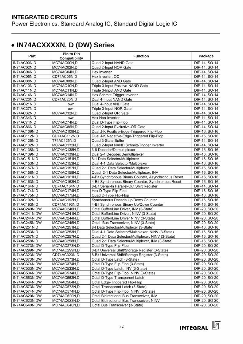
• IN74ACXXXXN, D (DW) Series Part Pin to Pin
Compatibility Function Package
IN74AC00N,D MC74AC00N,D Quad 2-Input NAND Gate DIP-14, SO-14IN74AC02N,D MC74AC02N,D Quad 2-Input NOR Gate DIP-14, SO-14IN74AC04N,D MC74AC04N,D Hex Inverter DIP-14, SO-14IN74AC05N,D CD74AC05N,D Hex Inverter, OC DIP-14, SO-14IN74AC08N,D MC74AC08N,D Quad 2-Input AND Gate DIP-14, SO-14IN74AC10N,D MC74AC10N,D Triple 3-Input Positive-NAND Gate DIP-14, SO-14IN74AC11N,D MC74AC11N,D Triple 3-Input AND Gate DIP-14, SO-14IN74AC14N,D MC74AC14N,D Hex Schmitt-Trigger Inverter DIP-14, SO-14IN74AC20N,D CD74AC20N,D Dual 4-Input NAND Gate DIP-14, SO-14IN74AC21N,D own Dual 4-Input AND Gate DIP-14, SO-14IN74AC27N,D own Triple 3-Input NOR Gate DIP-14, SO-14IN74AC32N,D MC74AC32N,D Quad 2-Input OR Gate DIP-14, SO-14IN74AC34N,D own Hex Non-Inverter DIP-14, SO-14IN74AC74N,D MC74AC74N,D Dual D-Type Flip-Flop DIP-14, SO-14IN74AC86N,D MC74AC86N,D Quad 2-Input Exclusive-OR Gate DIP-14, SO-14IN74AC109N,D MC74AC109N,D Dual J-K Positive-Edge-Triggered Flip-Flop DIP-16, SO-16IN74AC112N,D CD74AC112N,D Dual J-K Negative-Edge-Triggered Flip-Flop DIP-16, SO-16IN74AC125N,D T74AC125N,D Quad 3-State Buffer DIP-14, SO-14IN74AC132N,D MC74AC132N,D Quad 2-Input NAND Schmitt-Trigger Inverter DIP-14, SO-14IN74AC138N,D MC74AC138N,D 3-8 Decoder/Demultiplexer DIP-16, SO-16IN74AC139N,D MC74AC139N,D Dual 2-4 Decoder/Demultiplexer DIP-16, SO-16IN74AC151N,D MC74AC151N,D 8-1 Data Selector/Multiplexer DIP-16, SO-16IN74AC153N,D MC74AC153N,D Dual 4-1 Data Selector/Multiplexer DIP-16, SO-16IN74AC157N,D MC74AC157N,D Quad 2-1 Data Selector/Multiplexer DIP-16, SO-16IN74AC158N,D MC74AC158N,D Quad 2-1 Data Selector/Multiplexer, INV DIP-16, SO-16IN74AC161N,D MC74AC161N,D 4-Bit Synchronous Binary Counter, Asynchronous Reset DIP-16, SO-16IN74AC163N,D MC74AC163N,D 4-Bit Synchronous Binary Counter, Synchronous Reset DIP-16, SO-16IN74AC164N,D CD74AC164N,D 8-Bit Serial-In Parallel-Out Shift Register DIP-14, SO-14IN74AC174N,D MC74AC174N,D Hex D-Type Flip-Flop DIP-16, SO-16IN74AC175N,D MC74AC175N,D Quad D-Type Flip-Flop DIP-16, SO-16IN74AC192N,D MC74AC192N,D Synchronous Decade Up/Down Counter DIP-16, SO-16IN74AC193N,D CD74AC193N,D 4-Bit Synchronous Binary Up/Down Counter DIP-16, SO-16IN74AC240N,DW MC74AC240N,D Octal Buffer/Line Driver, INV (3-State) DIP-20, SO-20IN74AC241N,DW MC74AC241N,D Octal Buffer/Line Driver, NINV (3-State) DIP-20, SO-20IN74AC244N,DW MC74AC244N,D Octal Buffer/Line Driver NINV (3-State) DIP-20, SO-20IN74AC245N,DW MC74AC245N,D Octal Bus Transceiver, NINV (3-State) DIP-20, SO-20IN74AC251N,D MC74AC251N,D 8-I Data Selector/Multiplexer (3-State) DIP-16, SO-16IN74AC253N,D MC74AC253N,D Dual 4-1 Data Selector/Multiplexer, NINV (3-State) DIP-16, SO-16IN74AC257N,D MC74AC257N,D Quad 2-1 Data Selector/Multiplexer, NINV (3-State) DIP-16, SO-16IN74AC258N,D MC74AC258N,D Quad 2-1 Data Selector/Multiplexer, INV (3-State) DIP-16, SO-16IN74AC273N,DW MC74AC273N,D Octal D-Type Flip-Flop DIP-20, SO-20IN74AC299N,DW MC74AC299N,D 8-Bit Universal Shift/Storage Register (3-State) DIP-20, SO-20IN74AC323N,DW CD74AC323N,D 8-Bit Universal Shift/Storage Register (3-State) DIP-20, SO-20IN74AC373N,DW MC74AC373N,D Octal D-Type Latch (3-State) DIP-20, SO-20IN74AC374N,DW MC74AC374N,D Octal D-Type Flip-Flop (3-State) DIP-20, SO-20IN74AC533N,DW MC74AC533N,D Octal D-Type Latch, INV (3-State) DIP-20, SO-20IN74AC534N,DW MC74AC534N,D Octal D-Type Flip-Flop, NINV (3-State) DIP-20, SO-20IN74AC563N,DW MC74AC563N,D Octal D-Type Transparent Latch DIP-20, SO-20IN74AC564N,DW MC74AC564N,D Octal Edge-Triggered Flip-Flop DIP-20, SO-20IN74AC573N,DW MC74AC573N,D Octal Transparent Latch (3-State) DIP-20, SO-20IN74AC574N,DW MC74AC574N,D Octal D-Type Flip-Flop, NINV (3-State) DIP-20, SO-20IN74AC620N,DW MC74AC620N,D Octal Bidirectional Bus Transceiver, INV DIP-20, SO-20IN74AC623N,DW MC74AC623N,D Octal Bidirectional Bus Transceiver, NINV DIP-20, SO-20IN74AC640N,DW MC74AC640N,D Octal Bus Transceiver (3-State) DIP-20, SO-20
INTEGRATED CIRCUITS Standard Digital Logic IC
33
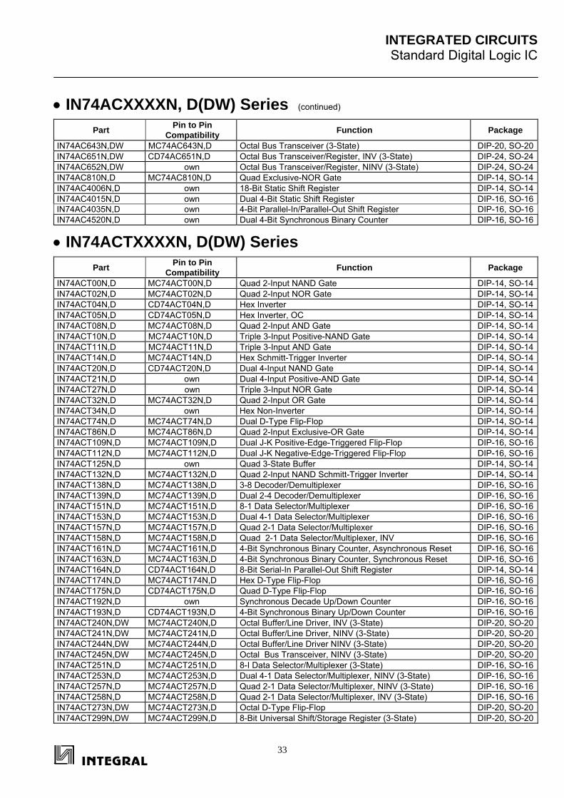
• IN74ACXXXXN, D(DW) Series (continued)
Part Pin to Pin Compatibility Function Package
IN74AC643N,DW MC74AC643N,D Octal Bus Transceiver (3-State) DIP-20, SO-20IN74AC651N,DW CD74AC651N,D Octal Bus Transceiver/Register, INV (3-State) DIP-24, SO-24IN74AC652N,DW own Octal Bus Transceiver/Register, NINV (3-State) DIP-24, SO-24IN74AC810N,D MC74AC810N,D Quad Exclusive-NOR Gate DIP-14, SO-14IN74AC4006N,D own 18-Bit Static Shift Register DIP-14, SO-14IN74AC4015N,D own Dual 4-Bit Static Shift Register DIP-16, SO-16IN74AC4035N,D own 4-Bit Parallel-In/Parallel-Out Shift Register DIP-16, SO-16IN74AC4520N,D own Dual 4-Bit Synchronous Binary Counter DIP-16, SO-16
• IN74ACTXXXXN, D(DW) Series Part Pin to Pin
Compatibility Function Package
IN74ACT00N,D MC74ACT00N,D Quad 2-Input NAND Gate DIP-14, SO-14IN74ACT02N,D MC74ACT02N,D Quad 2-Input NOR Gate DIP-14, SO-14IN74ACT04N,D CD74ACT04N,D Hex Inverter DIP-14, SO-14IN74ACT05N,D CD74ACT05N,D Hex Inverter, OC DIP-14, SO-14IN74ACT08N,D MC74ACT08N,D Quad 2-Input AND Gate DIP-14, SO-14IN74ACT10N,D MC74ACT10N,D Triple 3-Input Positive-NAND Gate DIP-14, SO-14IN74ACT11N,D MC74ACT11N,D Triple 3-Input AND Gate DIP-14, SO-14IN74ACT14N,D MC74ACT14N,D Hex Schmitt-Trigger Inverter DIP-14, SO-14IN74ACT20N,D CD74ACT20N,D Dual 4-Input NAND Gate DIP-14, SO-14IN74ACT21N,D own Dual 4-Input Positive-AND Gate DIP-14, SO-14IN74ACT27N,D own Triple 3-Input NOR Gate DIP-14, SO-14IN74ACT32N,D MC74ACT32N,D Quad 2-Input OR Gate DIP-14, SO-14IN74ACT34N,D own Hex Non-Inverter DIP-14, SO-14IN74ACT74N,D MC74ACT74N,D Dual D-Type Flip-Flop DIP-14, SO-14IN74ACT86N,D MC74ACT86N,D Quad 2-Input Exclusive-OR Gate DIP-14, SO-14IN74ACT109N,D MC74ACT109N,D Dual J-K Positive-Edge-Triggered Flip-Flop DIP-16, SO-16IN74ACT112N,D MC74ACT112N,D Dual J-K Negative-Edge-Triggered Flip-Flop DIP-16, SO-16IN74ACT125N,D own Quad 3-State Buffer DIP-14, SO-14IN74ACT132N,D MC74ACT132N,D Quad 2-Input NAND Schmitt-Trigger Inverter DIP-14, SO-14IN74ACT138N,D MC74ACT138N,D 3-8 Decoder/Demultiplexer DIP-16, SO-16IN74ACT139N,D MC74ACT139N,D Dual 2-4 Decoder/Demultiplexer DIP-16, SO-16IN74ACT151N,D MC74ACT151N,D 8-1 Data Selector/Multiplexer DIP-16, SO-16IN74ACT153N,D MC74ACT153N,D Dual 4-1 Data Selector/Multiplexer DIP-16, SO-16IN74ACT157N,D MC74ACT157N,D Quad 2-1 Data Selector/Multiplexer DIP-16, SO-16IN74ACT158N,D MC74ACT158N,D Quad 2-1 Data Selector/Multiplexer, INV DIP-16, SO-16IN74ACT161N,D MC74ACT161N,D 4-Bit Synchronous Binary Counter, Asynchronous Reset DIP-16, SO-16IN74ACT163N,D MC74ACT163N,D 4-Bit Synchronous Binary Counter, Synchronous Reset DIP-16, SO-16IN74ACT164N,D CD74ACT164N,D 8-Bit Serial-In Parallel-Out Shift Register DIP-14, SO-14IN74ACT174N,D MC74ACT174N,D Hex D-Type Flip-Flop DIP-16, SO-16IN74ACT175N,D CD74ACT175N,D Quad D-Type Flip-Flop DIP-16, SO-16IN74ACT192N,D own Synchronous Decade Up/Down Counter DIP-16, SO-16IN74ACT193N,D CD74ACT193N,D 4-Bit Synchronous Binary Up/Down Counter DIP-16, SO-16IN74ACT240N,DW MC74ACT240N,D Octal Buffer/Line Driver, INV (3-State) DIP-20, SO-20IN74ACT241N,DW MC74ACT241N,D Octal Buffer/Line Driver, NINV (3-State) DIP-20, SO-20IN74ACT244N,DW MC74ACT244N,D Octal Buffer/Line Driver NINV (3-State) DIP-20, SO-20IN74ACT245N,DW MC74ACT245N,D Octal Bus Transceiver, NINV (3-State) DIP-20, SO-20IN74ACT251N,D MC74ACT251N,D 8-I Data Selector/Multiplexer (3-State) DIP-16, SO-16IN74ACT253N,D MC74ACT253N,D Dual 4-1 Data Selector/Multiplexer, NINV (3-State) DIP-16, SO-16IN74ACT257N,D MC74ACT257N,D Quad 2-1 Data Selector/Multiplexer, NINV (3-State) DIP-16, SO-16IN74ACT258N,D MC74ACT258N,D Quad 2-1 Data Selector/Multiplexer, INV (3-State) DIP-16, SO-16IN74ACT273N,DW MC74ACT273N,D Octal D-Type Flip-Flop DIP-20, SO-20IN74ACT299N,DW MC74ACT299N,D 8-Bit Universal Shift/Storage Register (3-State) DIP-20, SO-20
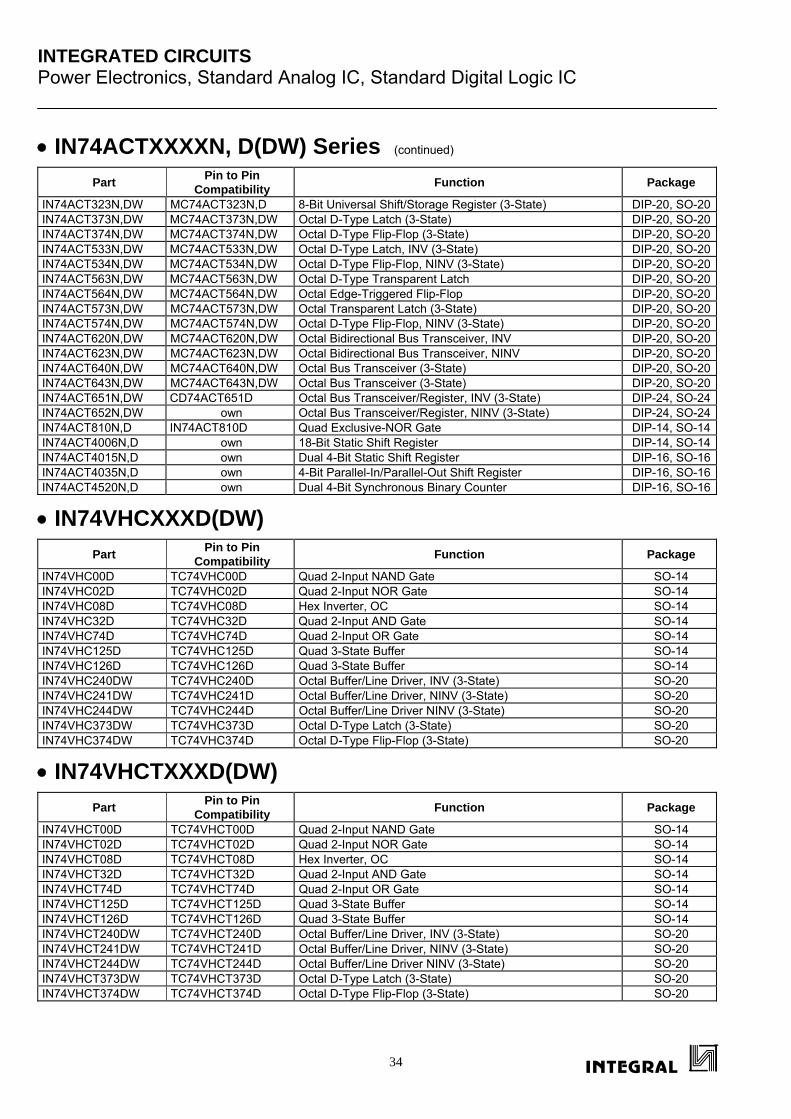
INTEGRATED CIRCUITS Power Electronics, Standard Analog IC, Standard Digital Logic IC
34
• IN74ACTXXXXN, D(DW) Series (continued)
Part Pin to Pin Compatibility Function Package
IN74ACT323N,DW MC74ACT323N,D 8-Bit Universal Shift/Storage Register (3-State) DIP-20, SO-20IN74ACT373N,DW MC74ACT373N,DW Octal D-Type Latch (3-State) DIP-20, SO-20IN74ACT374N,DW MC74ACT374N,DW Octal D-Type Flip-Flop (3-State) DIP-20, SO-20IN74ACT533N,DW MC74ACT533N,DW Octal D-Type Latch, INV (3-State) DIP-20, SO-20IN74ACT534N,DW MC74ACT534N,DW Octal D-Type Flip-Flop, NINV (3-State) DIP-20, SO-20IN74ACT563N,DW MC74ACT563N,DW Octal D-Type Transparent Latch DIP-20, SO-20IN74ACT564N,DW MC74ACT564N,DW Octal Edge-Triggered Flip-Flop DIP-20, SO-20IN74ACT573N,DW MC74ACT573N,DW Octal Transparent Latch (3-State) DIP-20, SO-20IN74ACT574N,DW MC74ACT574N,DW Octal D-Type Flip-Flop, NINV (3-State) DIP-20, SO-20IN74ACT620N,DW MC74ACT620N,DW Octal Bidirectional Bus Transceiver, INV DIP-20, SO-20IN74ACT623N,DW MC74ACT623N,DW Octal Bidirectional Bus Transceiver, NINV DIP-20, SO-20IN74ACT640N,DW MC74ACT640N,DW Octal Bus Transceiver (3-State) DIP-20, SO-20IN74ACT643N,DW MC74ACT643N,DW Octal Bus Transceiver (3-State) DIP-20, SO-20IN74ACT651N,DW CD74ACT651D Octal Bus Transceiver/Register, INV (3-State) DIP-24, SO-24IN74ACT652N,DW own Octal Bus Transceiver/Register, NINV (3-State) DIP-24, SO-24IN74ACT810N,D IN74ACT810D Quad Exclusive-NOR Gate DIP-14, SO-14IN74ACT4006N,D own 18-Bit Static Shift Register DIP-14, SO-14IN74ACT4015N,D own Dual 4-Bit Static Shift Register DIP-16, SO-16IN74ACT4035N,D own 4-Bit Parallel-In/Parallel-Out Shift Register DIP-16, SO-16IN74ACT4520N,D own Dual 4-Bit Synchronous Binary Counter DIP-16, SO-16
• IN74VHCXXXD(DW) Part Pin to Pin
Compatibility Function Package
IN74VHC00D TC74VHC00D Quad 2-Input NAND Gate SO-14 IN74VHC02D TC74VHC02D Quad 2-Input NOR Gate SO-14 IN74VHC08D TC74VHC08D Hex Inverter, OC SO-14 IN74VHC32D TC74VHC32D Quad 2-Input AND Gate SO-14 IN74VHC74D TC74VHC74D Quad 2-Input OR Gate SO-14 IN74VHC125D TC74VHC125D Quad 3-State Buffer SO-14 IN74VHC126D TC74VHC126D Quad 3-State Buffer SO-14 IN74VHC240DW TC74VHC240D Octal Buffer/Line Driver, INV (3-State) SO-20 IN74VHC241DW TC74VHC241D Octal Buffer/Line Driver, NINV (3-State) SO-20 IN74VHC244DW TC74VHC244D Octal Buffer/Line Driver NINV (3-State) SO-20 IN74VHC373DW TC74VHC373D Octal D-Type Latch (3-State) SO-20 IN74VHC374DW TC74VHC374D Octal D-Type Flip-Flop (3-State) SO-20
• IN74VHCTXXXD(DW) Part Pin to Pin
Compatibility Function Package
IN74VHCT00D TC74VHCT00D Quad 2-Input NAND Gate SO-14 IN74VHCT02D TC74VHCT02D Quad 2-Input NOR Gate SO-14 IN74VHCT08D TC74VHCT08D Hex Inverter, OC SO-14 IN74VHCT32D TC74VHCT32D Quad 2-Input AND Gate SO-14 IN74VHCT74D TC74VHCT74D Quad 2-Input OR Gate SO-14 IN74VHCT125D TC74VHCT125D Quad 3-State Buffer SO-14 IN74VHCT126D TC74VHCT126D Quad 3-State Buffer SO-14 IN74VHCT240DW TC74VHCT240D Octal Buffer/Line Driver, INV (3-State) SO-20 IN74VHCT241DW TC74VHCT241D Octal Buffer/Line Driver, NINV (3-State) SO-20 IN74VHCT244DW TC74VHCT244D Octal Buffer/Line Driver NINV (3-State) SO-20 IN74VHCT373DW TC74VHCT373D Octal D-Type Latch (3-State) SO-20 IN74VHCT374DW TC74VHCT374D Octal D-Type Flip-Flop (3-State) SO-20
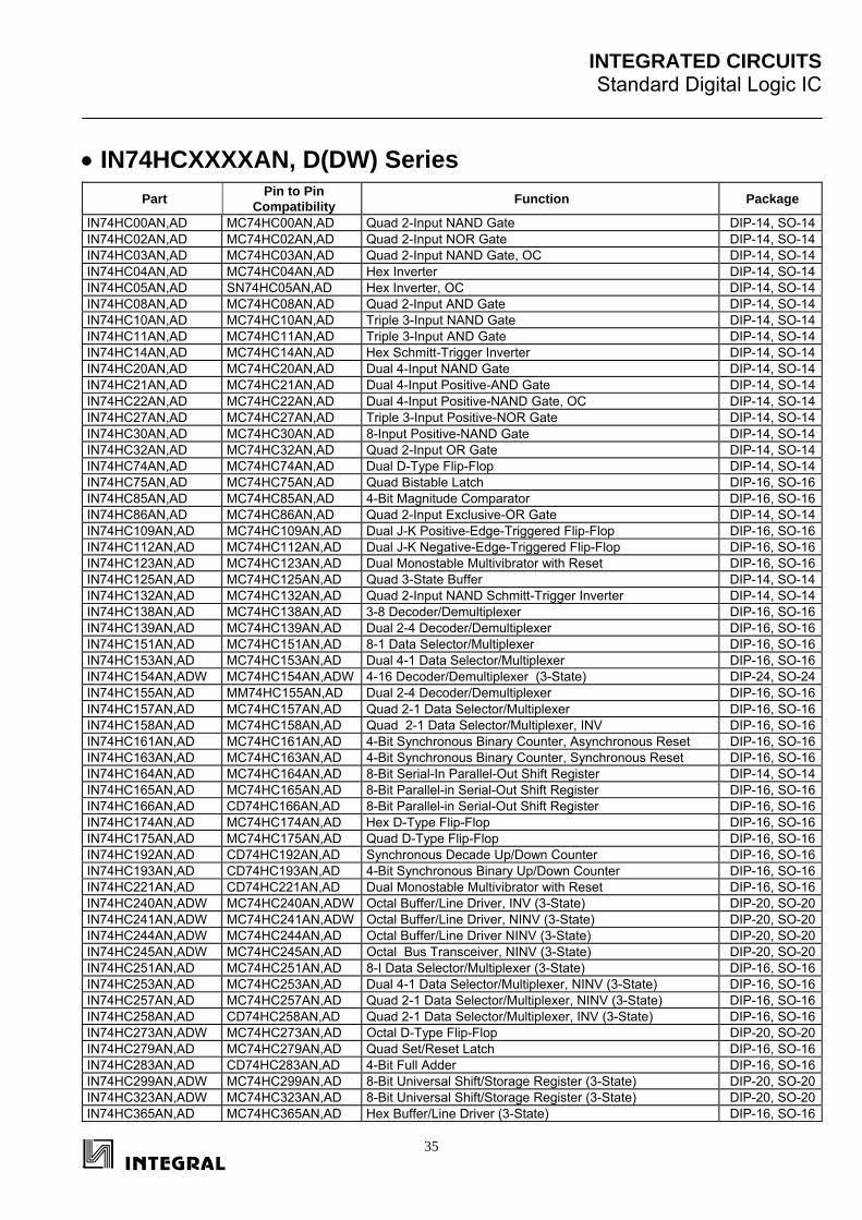
INTEGRATED CIRCUITS Standard Digital Logic IC
35
• IN74HCXXXXAN, D(DW) Series Part Pin to Pin
Compatibility Function Package
IN74HC00AN,AD MC74HC00AN,AD Quad 2-Input NAND Gate DIP-14, SO-14IN74HC02AN,AD MC74HC02AN,AD Quad 2-Input NOR Gate DIP-14, SO-14IN74HC03AN,AD MC74HC03AN,AD Quad 2-Input NAND Gate, OC DIP-14, SO-14IN74HC04AN,AD MC74HC04AN,AD Hex Inverter DIP-14, SO-14IN74HC05AN,AD SN74HC05AN,AD Hex Inverter, OC DIP-14, SO-14IN74HC08AN,AD MC74HC08AN,AD Quad 2-Input AND Gate DIP-14, SO-14IN74HC10AN,AD MC74HC10AN,AD Triple 3-Input NAND Gate DIP-14, SO-14IN74HC11AN,AD MC74HC11AN,AD Triple 3-Input AND Gate DIP-14, SO-14IN74HC14AN,AD MC74HC14AN,AD Hex Schmitt-Trigger Inverter DIP-14, SO-14IN74HC20AN,AD MC74HC20AN,AD Dual 4-Input NAND Gate DIP-14, SO-14IN74HC21AN,AD MC74HC21AN,AD Dual 4-Input Positive-AND Gate DIP-14, SO-14IN74HC22AN,AD MC74HC22AN,AD Dual 4-Input Positive-NAND Gate, OC DIP-14, SO-14IN74HC27AN,AD MC74HC27AN,AD Triple 3-Input Positive-NOR Gate DIP-14, SO-14IN74HC30AN,AD MC74HC30AN,AD 8-Input Positive-NAND Gate DIP-14, SO-14IN74HC32AN,AD MC74HC32AN,AD Quad 2-Input OR Gate DIP-14, SO-14IN74HC74AN,AD MC74HC74AN,AD Dual D-Type Flip-Flop DIP-14, SO-14IN74HC75AN,AD MC74HC75AN,AD Quad Bistable Latch DIP-16, SO-16IN74HC85AN,AD MC74HC85AN,AD 4-Bit Magnitude Comparator DIP-16, SO-16IN74HC86AN,AD MC74HC86AN,AD Quad 2-Input Exclusive-OR Gate DIP-14, SO-14IN74HC109AN,AD MC74HC109AN,AD Dual J-K Positive-Edge-Triggered Flip-Flop DIP-16, SO-16IN74HC112AN,AD MC74HC112AN,AD Dual J-K Negative-Edge-Triggered Flip-Flop DIP-16, SO-16IN74HC123AN,AD MC74HC123AN,AD Dual Monostable Multivibrator with Reset DIP-16, SO-16IN74HC125AN,AD MC74HC125AN,AD Quad 3-State Buffer DIP-14, SO-14IN74HC132AN,AD MC74HC132AN,AD Quad 2-Input NAND Schmitt-Trigger Inverter DIP-14, SO-14IN74HC138AN,AD MC74HC138AN,AD 3-8 Decoder/Demultiplexer DIP-16, SO-16IN74HC139AN,AD MC74HC139AN,AD Dual 2-4 Decoder/Demultiplexer DIP-16, SO-16IN74HC151AN,AD MC74HC151AN,AD 8-1 Data Selector/Multiplexer DIP-16, SO-16IN74HC153AN,AD MC74HC153AN,AD Dual 4-1 Data Selector/Multiplexer DIP-16, SO-16IN74HC154AN,ADW MC74HC154AN,ADW 4-16 Decoder/Demultiplexer (3-State) DIP-24, SO-24IN74HC155AN,AD MM74HC155AN,AD Dual 2-4 Decoder/Demultiplexer DIP-16, SO-16IN74HC157AN,AD MC74HC157AN,AD Quad 2-1 Data Selector/Multiplexer DIP-16, SO-16IN74HC158AN,AD MC74HC158AN,AD Quad 2-1 Data Selector/Multiplexer, INV DIP-16, SO-16IN74HC161AN,AD MC74HC161AN,AD 4-Bit Synchronous Binary Counter, Asynchronous Reset DIP-16, SO-16IN74HC163AN,AD MC74HC163AN,AD 4-Bit Synchronous Binary Counter, Synchronous Reset DIP-16, SO-16IN74HC164AN,AD MC74HC164AN,AD 8-Bit Serial-In Parallel-Out Shift Register DIP-14, SO-14IN74HC165AN,AD MC74HC165AN,AD 8-Bit Parallel-in Serial-Out Shift Register DIP-16, SO-16IN74HC166AN,AD CD74HC166AN,AD 8-Bit Parallel-in Serial-Out Shift Register DIP-16, SO-16IN74HC174AN,AD MC74HC174AN,AD Hex D-Type Flip-Flop DIP-16, SO-16IN74HC175AN,AD MC74HC175AN,AD Quad D-Type Flip-Flop DIP-16, SO-16IN74HC192AN,AD CD74HC192AN,AD Synchronous Decade Up/Down Counter DIP-16, SO-16IN74HC193AN,AD CD74HC193AN,AD 4-Bit Synchronous Binary Up/Down Counter DIP-16, SO-16IN74HC221AN,AD CD74HC221AN,AD Dual Monostable Multivibrator with Reset DIP-16, SO-16IN74HC240AN,ADW MC74HC240AN,ADW Octal Buffer/Line Driver, INV (3-State) DIP-20, SO-20IN74HC241AN,ADW MC74HC241AN,ADW Octal Buffer/Line Driver, NINV (3-State) DIP-20, SO-20IN74HC244AN,ADW MC74HC244AN,AD Octal Buffer/Line Driver NINV (3-State) DIP-20, SO-20IN74HC245AN,ADW MC74HC245AN,AD Octal Bus Transceiver, NINV (3-State) DIP-20, SO-20IN74HC251AN,AD MC74HC251AN,AD 8-I Data Selector/Multiplexer (3-State) DIP-16, SO-16IN74HC253AN,AD MC74HC253AN,AD Dual 4-1 Data Selector/Multiplexer, NINV (3-State) DIP-16, SO-16IN74HC257AN,AD MC74HC257AN,AD Quad 2-1 Data Selector/Multiplexer, NINV (3-State) DIP-16, SO-16IN74HC258AN,AD CD74HC258AN,AD Quad 2-1 Data Selector/Multiplexer, INV (3-State) DIP-16, SO-16IN74HC273AN,ADW MC74HC273AN,AD Octal D-Type Flip-Flop DIP-20, SO-20IN74HC279AN,AD MC74HC279AN,AD Quad Set/Reset Latch DIP-16, SO-16IN74HC283AN,AD CD74HC283AN,AD 4-Bit Full Adder DIP-16, SO-16IN74HC299AN,ADW MC74HC299AN,AD 8-Bit Universal Shift/Storage Register (3-State) DIP-20, SO-20IN74HC323AN,ADW MC74HC323AN,AD 8-Bit Universal Shift/Storage Register (3-State) DIP-20, SO-20IN74HC365AN,AD MC74HC365AN,AD Hex Buffer/Line Driver (3-State) DIP-16, SO-16
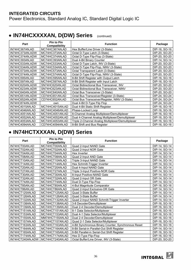
INTEGRATED CIRCUITS Power Electronics, Standard Analog IC, Standard Digital Logic IC
36
• IN74HCXXXXAN, D(DW) Series (continued) Part Pin to Pin
Compatibility Function Package
IN74HC367AN,AD MC74HC367AN,AD Hex Buffer/Line Driver (3-State) DIP-16, SO-16IN74HC373AN,ADW MC74HC373AN,AD Octal D-Type Latch (3-State) DIP-20, SO-20IN74HC374AN,ADW MC74HC374AN,AD Octal D-Type Flip-Flop (3-State) DIP-20, SO-20IN74HC393AN,AD MC74HC393AN,AD Dual 4-Bit Binary Counter DIP-14, SO-14IN74HC533AN,ADW MC74HC533AN,AD Octal D-Type Latch, INV (3-State) DIP-20, SO-20IN74HC534AN,ADW MC74HC534AN,AD Octal D-Type Flip-Flop, NINV (3-State) DIP-20, SO-20IN74HC573AN,ADW MC74HC573AN,AD Octal Transparent Latch (3-State) DIP-20, SO-20IN74HC574AN,ADW MC74HC574AN,AD Octal D-Type Flip-Flop, NINV (3-State) DIP-20, SO-20IN74HC595AN,AD MC74HC595AN,AD 8-Bit Shift Register with Output Latch DIP-16, SO-16IN74HC597AN,AD MC74HC597AN,AD 8-Bit Shift Register with Input Latch DIP-16, SO-16IN74HC620AN,ADW SN74HC620AN,AD Octal Bidirectional Bus Transceiver, INV DIP-20, SO-20IN74HC623AN,ADW SN74HC623AN,AD Octal Bidirectional Bus Transceiver, NINV DIP-20, SO-20IN74HC640AN,ADW MC74HC640AN,AD Octal Bus Transceiver (3-State) DIP-20, SO-20IN74HC651AN,ADW CD74HC651AN,AD Octal Bus Transceiver/Register (3-State) DIP-24, SO-24IN74HC652AN,ADW CD74HC652AN,AD Octal Bus Transceiver/Register, NINV (3-State) DIP-24, SO-24IN74HC874AN,ADW own Dual 4-Bit D-Type Flip Flop DIP-24, SO-24IN74HC4015AN,AD MC74HC4015AN,AD Dual 4-Bit Static Shift Register DIP-16, SO-16IN74HC4046AN,AD MC74HC4046AN,AD Phase-Locked Loop DIP-16, SO-16IN74HC4051AN,AD MC74HC4051AN,AD 8-Channel Analog Multiplexer/Demultiplexer DIP-16, SO-16IN74HC4052AN,AD MC74HC4052AN,AD Dual 4-Channel Analog Multiplexer/Demultiplexer DIP-16, SO-16IN74HC4053AN,AD MC74HC4053AN,AD Triple 2-Channel Analog Multiplexer/Demultiplexer DIP-16, SO-16IN74HC4094AN,AD CD74HC4094AN,AD 8-Bit Shift and Bus Register DIP-16, SO-16
• IN74HCTXXXAN, D(DW) Series Part Pin to Pin
Compatibility Function Package
IN74HCT00AN,AD MC74HCT00AN,AD Quad 2-Input NAND Gate DIP-14, SO-14IN74HCT02AN,AD MC74HCT02AN,AD Quad 2-Input NOR Gate DIP-14, SO-14IN74HCT04AN,AD MC74HCT04AN,AD Hex Inverter DIP-14, SO-14IN74HCT08AN,AD MC74HCT08AN,AD Quad 2-Input AND Gate DIP-14, SO-14IN74HCT10AN,AD MC74HCT10AN,AD Triple 3-Input NAND Gate DIP-14, SO-14IN74HCT14AN,AD MC74HCT14AN,AD Hex Schmitt-Trigger Inverter DIP-14, SO-14IN74HCT20AN,AD MC74HCT20AN,AD Dual 4-Input NAND Gate DIP-14, SO-14IN74HCT27AN,AD MC74HCT27AN,AD Triple 3-Input Positive-NOR Gate DIP-14, SO-14IN74HCT30AN,AD MC74HCT30AN,AD 8-Input Positive-NAND Gate DIP-14, SO-14IN74HCT32AN,AD MC74HCT32AN,AD Quad 2-Input OR Gate DIP-14, SO-14IN74HCT74AN,AD MC74HCT74AN,AD Dual D-Type Flip-Flop DIP-14, SO-14IN74HCT85AN,AD MC74HCT85AN,AD 4-But Magnitude Comparator DIP-16, SO-16IN74HCT86AN,AD MC74HCT86AN,AD Quad 2-Input Exclusive-OR Gate DIP-14, SO-14IN74HCT125AN,AD MC74HCT125AN,AD Quad 3-State Buffer DIP-14, SO-14IN74HCT126AN,AD MC74HCT126AN,AD Quad 3-State Buffer DIP-14, SO-14IN74HCT132AN,AD MC74HCT132AN,AD Quad 2-Input NAND Schmitt-Trigger Inverter DIP-14, SO-14IN74HCT138AN,AD MC74HCT138AN,AD 3-8 Decoder/Demultiplexer DIP-16, SO-16IN74HCT139AN,AD MC74HCT139AN,AD Dual 2-4 Decoder/Demultiplexer DIP-16, SO-16IN74HCT151AN,AD MC74HCT151AN,AD 8-1 Data Selector/Multiplexer DIP-16, SO-16IN74HCT153AN,AD MC74HCT153AN,AD Dual 4-1 Data Selector/Multiplexer DIP-16, SO-16IN74HCT155AN,AD MM74HCT155AN,AD Dual 2-4 Decoder/Demultiplexer DIP-16, SO-16IN74HCT157AN,AD MC74HCT157AN,AD Quad 2-1 Data Selector/Multiplexer DIP-16, SO-16IN74HCT163AN,AD MC74HCT163AN,AD 4-Bit Synchronous Binary Counter, Synchronous Reset DIP-16, SO-16IN74HCT164AN,AD MC74HCT164AN,AD 8-Bit Serial-in Parallel-Out Shift Register DIP-14, SO-14IN74HCT165AN,AD MC74HCT165AN,AD 8-Bit Parallel-in Serial-Out Shift Register DIP-16, SO-16IN74HCT174AN,AD MC74HCT174AN,AD Hex D-Type Flip-Flop DIP-16, SO-16IN74HCT240AN,ADW MC74HCT240AN,AD Octal Buffer/Line Driver, INV (3-State) DIP-20, SO-20
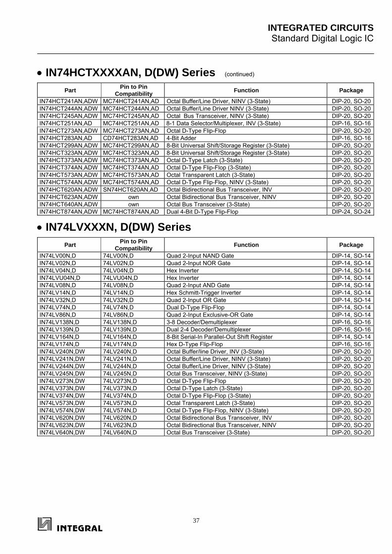
INTEGRATED CIRCUITS Standard Digital Logic IC
37
• IN74HCTXXXXAN, D(DW) Series (continued) Part Pin to Pin
Compatibility Function Package
IN74HCT241AN,ADW MC74HCT241AN,AD Octal Buffer/Line Driver, NINV (3-State) DIP-20, SO-20IN74HCT244AN,ADW MC74HCT244AN,AD Octal Buffer/Line Driver NINV (3-State) DIP-20, SO-20IN74HCT245AN,ADW MC74HCT245AN,AD Octal Bus Transceiver, NINV (3-State) DIP-20, SO-20IN74HCT251AN,AD MC74HCT251AN,AD 8-1 Data Selector/Multiplexer, INV (3-State) DIP-16, SO-16IN74HCT273AN,ADW MC74HCT273AN,AD Octal D-Type Flip-Flop DIP-20, SO-20IN74HCT283AN,AD CD74HCT283AN,AD 4-Bit Adder DIP-16, SO-16IN74HCT299AN,ADW MC74HCT299AN,AD 8-Bit Universal Shift/Storage Register (3-State) DIP-20, SO-20IN74HCT323AN,ADW MC74HCT323AN,AD 8-Bit Universal Shift/Storage Register (3-State) DIP-20, SO-20IN74HCT373AN,ADW MC74HCT373AN,AD Octal D-Type Latch (3-State) DIP-20, SO-20IN74HCT374AN,ADW MC74HCT374AN,AD Octal D-Type Flip-Flop (3-State) DIP-20, SO-20IN74HCT573AN,ADW MC74HCT573AN,AD Octal Transparent Latch (3-State) DIP-20, SO-20IN74HCT574AN,ADW MC74HCT574AN,AD Octal D-Type Flip-Flop, NINV (3-State) DIP-20, SO-20IN74HCT620AN,ADW SN74HCT620AN,AD Octal Bidirectional Bus Transceiver, INV DIP-20, SO-20IN74HCT623AN,ADW own Octal Bidirectional Bus Transceiver, NINV DIP-20, SO-20IN74HCT640AN,ADW own Octal Bus Transceiver (3-State) DIP-20, SO-20IN74HCT874AN,ADW MC74HCT874AN,AD Dual 4-Bit D-Type Flip-Flop DIP-24, SO-24
• IN74LVXXXN, D(DW) Series Part Pin to Pin
Compatibility Function Package
IN74LV00N,D 74LV00N,D Quad 2-Input NAND Gate DIP-14, SO-14IN74LV02N,D 74LV02N,D Quad 2-Input NOR Gate DIP-14, SO-14IN74LV04N,D 74LV04N,D Hex Inverter DIP-14, SO-14IN74LVU04N,D 74LVU04N,D Hex Inverter DIP-14, SO-14IN74LV08N,D 74LV08N,D Quad 2-Input AND Gate DIP-14, SO-14IN74LV14N,D 74LV14N,D Hex Schmitt-Trigger Inverter DIP-14, SO-14IN74LV32N,D 74LV32N,D Quad 2-Input OR Gate DIP-14, SO-14IN74LV74N,D 74LV74N,D Dual D-Type Flip-Flop DIP-14, SO-14IN74LV86N,D 74LV86N,D Quad 2-Input Exclusive-OR Gate DIP-14, SO-14IN74LV138N,D 74LV138N,D 3-8 Decoder/Demultiplexer DIP-16, SO-16IN74LV139N,D 74LV139N,D Dual 2-4 Decoder/Demultiplexer DIP-16, SO-16IN74LV164N,D 74LV164N,D 8-Bit Serial-In Parallel-Out Shift Register DIP-14, SO-14IN74LV174N,D 74LV174N,D Hex D-Type Flip-Flop DIP-16, SO-16IN74LV240N,DW 74LV240N,D Octal Buffer/line Driver, INV (3-State) DIP-20, SO-20IN74LV241N,DW 74LV241N,D Octal Buffer/Line Driver, NINV (3-State) DIP-20, SO-20IN74LV244N,DW 74LV244N,D Octal Buffer/Line Driver, NINV (3-State) DIP-20, SO-20IN74LV245N,DW 74LV245N,D Octal Bus Transceiver, NINV (3-State) DIP-20, SO-20IN74LV273N,DW 74LV273N,D Octal D-Type Flip-Flop DIP-20, SO-20IN74LV373N,DW 74LV373N,D Octal D-Type Latch (3-State) DIP-20, SO-20IN74LV374N,DW 74LV374N,D Octal D-Type Flip-Flop (3-State) DIP-20, SO-20IN74LV573N,DW 74LV573N,D Octal Transparent Latch (3-State) DIP-20, SO-20IN74LV574N,DW 74LV574N,D Octal D-Type Flip-Flop, NINV (3-State) DIP-20, SO-20IN74LV620N,DW 74LV620N,D Octal Bidirectional Bus Transceiver, INV DIP-20, SO-20IN74LV623N,DW 74LV623N,D Octal Bidirectional Bus Transceiver, NINV DIP-20, SO-20IN74LV640N,DW 74LV640N,D Octal Bus Transceiver (3-State) DIP-20, SO-20

INTEGRATED CIRCUITS Power Electronics, Standard Analog IC, Standard Digital Logic IC
38
• IN74XXXN, D Series Part Pin to Pin
Compatibility Function Package
IN7401N SN7401N Quad 2-Input NAND Gate, OC DIP-14 IN7406N,D SN7406N,D Hex Inverter/Buffer with High-Voltage Output, OC DIP-14, SO-14IN7420N SN7420N Dual 4-Input NAND Gate DIP-14 IN7450N SN7450N Dual 2-Wide 2-Input AND-OR-Invert Gate DIP-14 IN7472N SN7472N J-K Flip-Flop DIP-14 IN74141N SN74141N BCD-to-Decimal Decoder/Driver DIP-16 IN74145N SN74145N BCD-to-Decimal Decoder, OC DIP-16 IN74154N SN74154N 4-16 Decoder/Demultiplexer DIP-24 IN74175N SN74175N Quad D-Type Flip-Flop DIP-16
• IN74LSXXXN, D(DW) Series Part Pin to Pin
Compatibility Function Package
IN74LS04N,D CD74LS04N,D Hex Inverter DIP-14, SO-14IN74LS05N,D CD74LS05N,D Hex Inverter, OC DIP-14, SO-14IN74LS06N,D CD74LS06N,D Hex Inverter/Buffer with High-Voltage Output, OC DIP-14, SO-14IN74LS07N,D CD74LS07N,D Hex Buffer with High-Voltage Output, OC, 30 V DIP-14, SO-14IN74LS14N,D CD74LS14N,D Hex Schmitt-Trigger Inverter DIP-14, SO-14IN74LS86N,D CD74LS86N,D Quad 2-Input Exclusive-OR Gate DIP-14, SO-14IN74LS138N,D CD74LS138N,D 3-8 Decoder/Demultiplexer DIP-16, SO-16IN74LS157N,D CD74LS157N,D Quad 2-1 Data Selector/Multiplexer DIP-16, SO-16IN74LS161AN,AD CD74LS161AN,AD 4-Bit Binary Counter DIP-16, SO-16IN74LS164N,D CD74LS164N,D 8-Bit Parallel-Out Shift Register DIP-14, SO-14IN74LS244N,DW CD74LS244N,DW Octal Buffer/Line Driver, NINV (3-State) DIP-20, SO-20IN74LS245N,DW CD74LS245N,DW Octal Bus Transceiver, NINV (3-State) DIP-20, SO-20
• IN74ALSXXXXN, D(DW) Series Part Pin to Pin
Compatibility Function Package
IN74ALS00AN,AD SN74ALS00AN,AD Quad 2-Input Positive-NAND Gate DIP-14, SO-14IN74ALS01N,D SN74ALS01N,D Quad 2-Input Positive-NAND Gate, OC DIP-14, SO-14IN74ALS02N,D SN74ALS02N,D Quad 2-Input Positive-NOR Gate DIP-14, SO-14IN74ALS03AN,AD SN74ALS03AN,AD Quad 2-Input Positive-NAND Gate, OC DIP-14, SO-14IN74ALS04AN,AD SN74ALS04AN,AD Hex Inverter DIP-14, SO-14IN74ALS05AN,AD SN74ALS05AN,AD Hex Inverter, OC DIP-14, SO-14IN74ALS08N,D SN74ALS08N,D Quad 2-Input Positive-AND Gate DIP-14, SO-14IN74ALS09N,D SN74ALS09N,D Quad 2-Input Positive-AND Gate, OC DIP-14, SO-14IN74ALS10AN,AD SN74ALS10AN,AD Triple 3-Input Positive-NAND Gate DIP-14, SO-14IN74ALS11AN,AD SN74ALS11AN,AD Triple 3-Input Positive-AND Gate DIP-14, SO-14IN74ALS12AN,AD SN74ALS12AN,AD Triple 3-Input Positive-NAND Gate, OC DIP-14, SO-14IN74ALS14N,D SN74ALS14N,D Hex Schmitt-Trigger Inverter DIP-14, SO-14IN74ALS15AN,AD SN74ALS15AN,AD Triple 3-Input Positive-AND Gate, OC DIP-14, SO-14IN74ALS20AN,AD SN74ALS20AN,AD Dual 4-Input Positive-NAND Gate DIP-14, SO-14IN74ALS21N,AD SN74ALS21N,AD Dual 4-Input Positive-AND Gate DIP-14, SO-14IN74ALS22BN,BD SN74ALS22BN,BD Dual 4-Input Positive-NAND Gate, OC DIP-14, SO-14IN74ALS27N,D SN74ALS27N,D Triple 3-Input Positive-NOR Gate DIP-14, SO-14IN74ALS30AN,AD SN74ALS30AN,AD 8-Input Positive-NAND Gate DIP-14, SO-14IN74ALS32N,D SN74ALS32N,D Quad 2-Input Positive-OR Gate DIP-14, SO-14IN74ALS33AN,AD SN74ALS33AN,AD Quad 2-Input Positive-NOR Buffer, OC DIP-14, SO-14
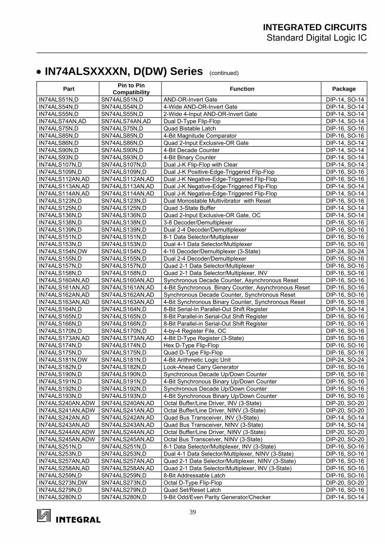
INTEGRATED CIRCUITS Standard Digital Logic IC
39
• IN74ALSXXXXN, D(DW) Series (continued)
Part Pin to Pin Compatibility Function Package
IN74ALS51N,D SN74ALS51N,D AND-OR-Invert Gate DIP-14, SO-14IN74ALS54N,D SN74ALS54N,D 4-Wide AND-OR-Invert Gate DIP-14, SO-14IN74ALS55N,D SN74ALS55N,D 2-Wide 4-Input AND-OR-Invert Gate DIP-14, SO-14IN74ALS74AN,AD SN74ALS74AN,AD Dual D-Type Flip-Flop DIP-14, SO-14IN74ALS75N,D SN74ALS75N,D Quad Bistable Latch DIP-16, SO-16IN74ALS85N,D SN74ALS85N,D 4-Bit Magnitude Comparator DIP-16, SO-16IN74ALS86N,D SN74ALS86N,D Quad 2-Input Exclusive-OR Gate DIP-14, SO-14IN74ALS90N,D SN74ALS90N,D 4-Bit Decade Counter DIP-14, SO-14IN74ALS93N,D SN74ALS93N,D 4-Bit Binary Counter DIP-14, SO-14IN74ALS107N,D SN74ALS107N,D Dual J-K Flip-Flop with Clear DIP-14, SO-14IN74ALS109N,D SN74ALS109N,D Dual J-K Positive-Edge-Triggered Flip-Flop DIP-16, SO-16IN74ALS112AN,AD SN74ALS112AN,AD Dual J-K Negative-Edge-Triggered Flip-Flop DIP-16, SO-16IN74ALS113AN,AD SN74ALS113AN,AD Dual J-K Negative-Edge-Triggered Flip-Flop DIP-14, SO-14IN74ALS114AN,AD SN74ALS114AN,AD Dual J-K Negative-Edge-Triggered Flip-Flop DIP-14, SO-14IN74ALS123N,D SN74ALS123N,D Dual Monostable Multivibrator with Reset DIP-16, SO-16IN74ALS125N,D SN74ALS125N,D Quad 3-State Buffer DIP-14, SO-14IN74ALS136N,D SN74ALS136N,D Quad 2-Input Exclusive-OR Gate, OC DIP-14, SO-14IN74ALS138N,D SN74ALS138N,D 3-8 Decoder/Demultiplexer DIP-16, SO-16IN74ALS139N,D SN74ALS139N,D Dual 2-4 Decoder/Demultiplexer DIP-16, SO-16IN74ALS151N,D SN74ALS151N,D 8-1 Data Selector/Multiplexer DIP-16, SO-16IN74ALS153N,D SN74ALS153N,D Dual 4-1 Data Selector/Multiplexer DIP-16, SO-16IN74ALS154N,DW SN74ALS154N,D 4-16 Decoder/Demultiplexer (3-State) DIP-24, SO-24IN74ALS155N,D SN74ALS155N,D Dual 2-4 Decoder/Demultiplexer DIP-16, SO-16IN74ALS157N,D SN74ALS157N,D Quad 2-1 Data Selector/Multiplexer DIP-16, SO-16IN74ALS158N,D SN74ALS158N,D Quad 2-1 Data Selector/Multiplexer, INV DIP-16, SO-16IN74ALS160AN,AD SN74ALS160AN,AD Synchronous Decade Counter, Asynchronous Reset DIP-16, SO-16IN74ALS161AN,AD SN74ALS161AN,AD 4-Bit Synchronous Binary Counter, Asynchronous Reset DIP-16, SO-16IN74ALS162AN,AD SN74ALS162AN,AD Synchronous Decade Counter, Synchronous Reset DIP-16, SO-16IN74ALS163AN,AD SN74ALS163AN,AD 4-Bit Synchronous Binary Counter, Synchronous Reset DIP-16, SO-16IN74ALS164N,D SN74ALS164N,D 8-Bit Serial-In Parallel-Out Shift Register DIP-14, SO-14IN74ALS165N,D SN74ALS165N,D 8-Bit Parallel-in Serial-Out Shift Register DIP-16, SO-16IN74ALS166N,D SN74ALS166N,D 8-Bit Parallel-in Serial-Out Shift Register DIP-16, SO-16IN74ALS170N,D SN74ALS170N,D 4-by-4 Register File, OC DIP-16, SO-16IN74ALS173AN,AD SN74ALS173AN,AD 4-Bit D-Type Register (3-State) DIP-16, SO-16IN74ALS174N,D SN74ALS174N,D Hex D-Type Flip-Flop DIP-16, SO-16IN74ALS175N,D SN74ALS175N,D Quad D-Type Flip-Flop DIP-16, SO-16IN74ALS181N,DW SN74ALS181N,D 4-Bit Arithmetic Logic Unit DIP-24, SO-24IN74ALS182N,D SN74ALS182N,D Look-Ahead Carry Generator DIP-16, SO-16IN74ALS190N,D SN74ALS190N,D Synchronous Decade Up/Down Counter DIP-16, SO-16IN74ALS191N,D SN74ALS191N,D 4-Bit Synchronous Binary Up/Down Counter DIP-16, SO-16IN74ALS192N,D SN74ALS192N,D Synchronous Decade Up/Down Counter DIP-16, SO-16IN74ALS193N,D SN74ALS193N,D 4-Bit Synchronous Binary Up/Down Counter DIP-16, SO-16IN74ALS240AN,ADW SN74ALS240AN,AD Octal Buffer/Line Driver, INV (3-State) DIP-20, SO-20IN74ALS241AN,ADW SN74ALS241AN,AD Octal Buffer/Line Driver, NINV (3-State) DIP-20, SO-20IN74ALS242AN,AD SN74ALS242AN,AD Quad Bus Transceiver, INV (3-State) DIP-14, SO-14IN74ALS243AN,AD SN74ALS243AN,AD Quad Bus Transceiver, NINV (3-State) DIP-14, SO-14IN74ALS244AN,ADW SN74ALS244AN,AD Octal Buffer/Line Driver, NINV (3-State) DIP-20, SO-20IN74ALS245AN,ADW SN74ALS245AN,AD Octal Bus Transceiver, NINV (3-State) DIP-20, SO-20IN74ALS251N,D SN74ALS251N,D 8-1 Data Selector/Multiplexer, INV (3-State) DIP-16, SO-16IN74ALS253N,D SN74ALS253N,D Dual 4-1 Data Selector/Multiplexer, NINV (3-State) DIP-16, SO-16IN74ALS257AN,AD SN74ALS257AN,AD Quad 2-1 Data Selector/Multiplexer, NINV (3-State) DIP-16, SO-16IN74ALS258AN,AD SN74ALS258AN,AD Quad 2-1 Data Selector/Multiplexer, INV (3-State) DIP-16, SO-16IN74ALS259N,D SN74ALS259N,D 8-Bit Addressable Latch DIP-16, SO-16IN74ALS273N,DW SN74ALS273N,D Octal D-Type Flip-Flop DIP-20, SO-20IN74ALS279N,D SN74ALS279N,D Quad Set/Reset Latch DIP-16, SO-16IN74ALS280N,D SN74ALS280N,D 9-Bit Odd/Even Parity Generator/Checker DIP-14, SO-14
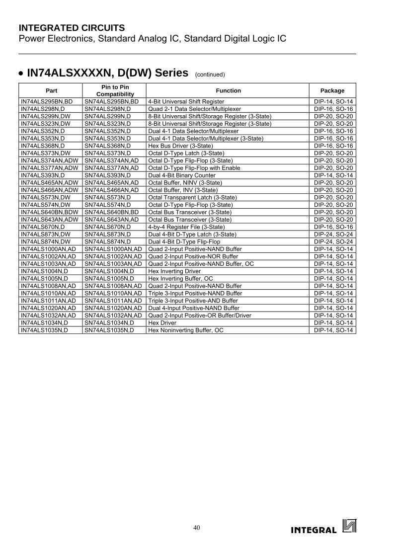
INTEGRATED CIRCUITS Power Electronics, Standard Analog IC, Standard Digital Logic IC
40
• IN74ALSXXXXN, D(DW) Series (continued)
Part Pin to Pin Compatibility Function Package
IN74ALS295BN,BD SN74ALS295BN,BD 4-Bit Universal Shift Register DIP-14, SO-14IN74ALS298N,D SN74ALS298N,D Quad 2-1 Data Selector/Multiplexer DIP-16, SO-16IN74ALS299N,DW SN74ALS299N,D 8-Bit Universal Shift/Storage Register (3-State) DIP-20, SO-20IN74ALS323N,DW SN74ALS323N,D 8-Bit Universal Shift/Storage Register (3-State) DIP-20, SO-20IN74ALS352N,D SN74ALS352N,D Dual 4-1 Data Selector/Multiplexer DIP-16, SO-16IN74ALS353N,D SN74ALS353N,D Dual 4-1 Data Selector/Multiplexer (3-State) DIP-16, SO-16IN74ALS368N,D SN74ALS368N,D Hex Bus Driver (3-State) DIP-16, SO-16IN74ALS373N,DW SN74ALS373N,D Octal D-Type Latch (3-State) DIP-20, SO-20IN74ALS374AN,ADW SN74ALS374AN,AD Octal D-Type Flip-Flop (3-State) DIP-20, SO-20IN74ALS377AN,ADW SN74ALS377AN,AD Octal D-Type Flip-Flop with Enable DIP-20, SO-20IN74ALS393N,D SN74ALS393N,D Dual 4-Bit Binary Counter DIP-14, SO-14IN74ALS465AN,ADW SN74ALS465AN,AD Octal Buffer, NINV (3-State) DIP-20, SO-20IN74ALS466AN,ADW SN74ALS466AN,AD Octal Buffer, INV (3-State) DIP-20, SO-20IN74ALS573N,DW SN74ALS573N,D Octal Transparent Latch (3-State) DIP-20, SO-20IN74ALS574N,DW SN74ALS574N,D Octal D-Type Flip-Flop (3-State) DIP-20, SO-20IN74ALS640BN,BDW SN74ALS640BN,BD Octal Bus Transceiver (3-State) DIP-20, SO-20IN74ALS643AN,ADW SN74ALS643AN,AD Octal Bus Transceiver (3-State) DIP-20, SO-20IN74ALS670N,D SN74ALS670N,D 4-by-4 Register File (3-State) DIP-16, SO-16IN74ALS873N,DW SN74ALS873N,D Dual 4-Bit D-Type Latch (3-State) DIP-24, SO-24IN74ALS874N,DW SN74ALS874N,D Dual 4-Bit D-Type Flip-Flop DIP-24, SO-24IN74ALS1000AN,AD SN74ALS1000AN,AD Quad 2-Input Positive-NAND Buffer DIP-14, SO-14IN74ALS1002AN,AD SN74ALS1002AN,AD Quad 2-Input Positive-NOR Buffer DIP-14, SO-14IN74ALS1003AN,AD SN74ALS1003AN,AD Quad 2-Input Positive-NAND Buffer, OC DIP-14, SO-14IN74ALS1004N,D SN74ALS1004N,D Hex Inverting Driver DIP-14, SO-14IN74ALS1005N,D SN74ALS1005N,D Hex Inverting Buffer, OC DIP-14, SO-14IN74ALS1008AN,AD SN74ALS1008AN,AD Quad 2-Input Positive-NAND Buffer DIP-14, SO-14IN74ALS1010AN,AD SN74ALS1010AN,AD Triple 3-Input Positive-NAND Buffer DIP-14, SO-14IN74ALS1011AN,AD SN74ALS1011AN,AD Triple 3-Input Positive-AND Buffer DIP-14, SO-14IN74ALS1020AN,AD SN74ALS1020AN,AD Dual 4-Input Positive-NAND Buffer DIP-14, SO-14IN74ALS1032AN,AD SN74ALS1032AN,AD Quad 2-Input Positive-OR Buffer/Driver DIP-14, SO-14IN74ALS1034N,D SN74ALS1034N,D Hex Driver DIP-14, SO-14IN74ALS1035N,D SN74ALS1035N,D Hex Noninverting Buffer, OC DIP-14, SO-14
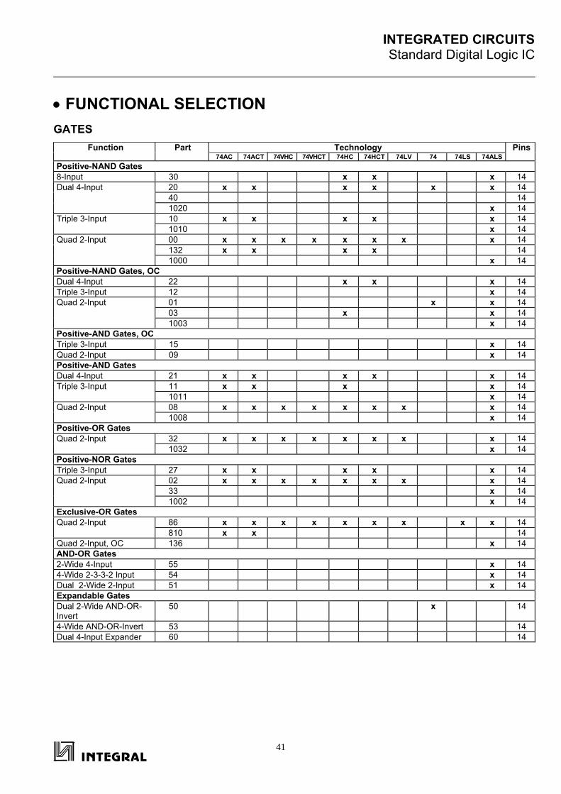
INTEGRATED CIRCUITS Standard Digital Logic IC
41
• FUNCTIONAL SELECTION GATES
Function Part Technology Pins 74AC 74ACT 74VHC 74VHCT 74HC 74HCT 74LV 74 74LS 74ALS
Positive-NAND Gates 8-Input 30 x х х 14 Dual 4-Input 20 х х x х x х 14 40 14 1020 х 14 Triple 3-Input 10 x х x х х 14 1010 х 14 Quad 2-Input 00 х х x x x х х х 14 132 х х x x 14 1000 x 14 Positive-NAND Gates, OC Dual 4-Input 22 х x х 14 Triple 3-Input 12 х 14 Quad 2-Input 01 x х 14 03 x х 14 1003 х 14 Positive-AND Gates, OC Triple 3-Input 15 х 14 Quad 2-Input 09 х 14 Positive-AND Gates Dual 4-Input 21 х х х х х 14 Triple 3-Input 11 х х x х 14 1011 х 14 Quad 2-Input 08 х x x x х x x х 14 1008 x 14 Positive-OR Gates Quad 2-Input 32 x x x x x x x х 14 1032 x 14 Positive-NOR Gates Triple 3-Input 27 х х x х х 14 Quad 2-Input 02 x x x x х x x х 14 33 х 14 1002 х 14 Exclusive-OR Gates Quad 2-Input 86 х х x x x x x x х 14 810 x x 14 Quad 2-Input, OC 136 х 14 AND-OR Gates 2-Wide 4-Input 55 х 14 4-Wide 2-3-3-2 Input 54 х 14 Dual 2-Wide 2-Input 51 х 14 Expandable Gates Dual 2-Wide AND-OR-Invert
50 x 14
4-Wide AND-OR-Invert 53 14 Dual 4-Input Expander 60 14

INTEGRATED CIRCUITS Standard Digital Logic IC
42
• FUNCTIONAL SELECTION (continued) HEX INVERTERS/NONINVERTERS
Function Part Technology Pins 74AC 74ACT 74VHC 74VHCT 74HC 74HCT 74LV 74 74LS 74ALS
Hex Inverters 04 х х х х х х х 14 U04 х 14 05 х х х х х 14 06 x х 14 14 х х x x x x х 14 16 14 1004 х 14 1005 x 14 Hex Noninverters 34 х x 14
DRIVERS AND BUS TRANSCEIVERS
Function Part Technology Pins 74AC 74ACT 74VHC 74VHCT 74HC 74HCT 74LV 74 74LS 74ALS
Hex Drivers Hex Drivers 07 x 14 1034 x 14 1035 x 14 Noninverting Hex 365 х 16 Buffers/Drivers 367 x 16 368 x 16 Drivers with 3-State Outputs Quad Buffer Drivers 125 х x х х x x x 14 126 х х х 14 Octal Buffer/Drivers, 241 х х х х х х x x 20 NINV 244 х х х х х х х x x 20 465 x 20
Octal Buffer Drivers, 240 x х x x х x х x 20 INV 466 x 20 Bus Transceivers with 3-State Outputs Quad Transceiver, NINV 243 x 14 Quad Transceiver, INV 242 x 14 Octal Transceiver 245 x x x x x x x 20 620 x x x x x 20 640 x x x x x x 20 643 x x x 20 Octal Bus Transceivers 651 x x x 24 with Registers 652 x x x 24 True Output Transceiver 623 x x x x x 20 50/75-Ohm Line Drivers Quad 2-Input Positive-NOR
128 14
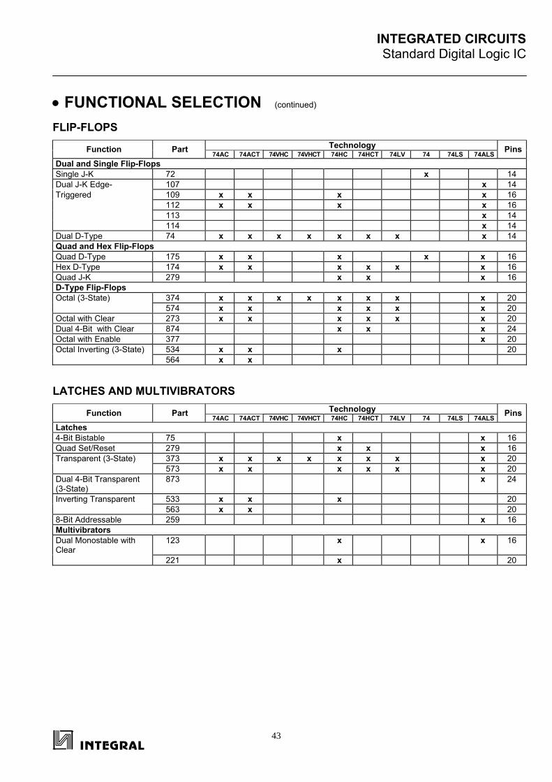
INTEGRATED CIRCUITS Standard Digital Logic IC
43
• FUNCTIONAL SELECTION (continued) FLIP-FLOPS
Function Part Technology Pins 74AC 74ACT 74VHC 74VHCT 74HC 74HCT 74LV 74 74LS 74ALS
Dual and Single Flip-Flops Single J-K 72 x 14 Dual J-K Edge- 107 x 14 Triggered 109 x x x x 16 112 x x x x 16 113 x 14 114 x 14 Dual D-Type 74 x x x x x x x x 14 Quad and Hex Flip-Flops Quad D-Type 175 x x x х х 16 Hex D-Type 174 x x x x x х 16 Quad J-K 279 x x x 16 D-Type Flip-Flops Octal (3-State) 374 x x x х x x x x 20 574 x x x x x x 20 Octal with Clear 273 x x x x x x 20 Dual 4-Bit with Clear 874 x x x 24 Octal with Enable 377 x 20 Octal Inverting (3-State) 534 x x x 20 564 x x
LATCHES AND MULTIVIBRATORS
Function Part Technology Pins 74AC 74ACT 74VHC 74VHCT 74HC 74HCT 74LV 74 74LS 74ALS
Latches 4-Bit Bistable 75 x x 16 Quad Set/Reset 279 x x x 16 Transparent (3-State) 373 x x x x x x x x 20 573 x x x x x x 20 Dual 4-Bit Transparent (3-State)
873 x 24
Inverting Transparent 533 x x x 20 563 x x 20 8-Bit Addressable 259 x 16 Multivibrators Dual Monostable with Clear
123 x x 16
221 x 20
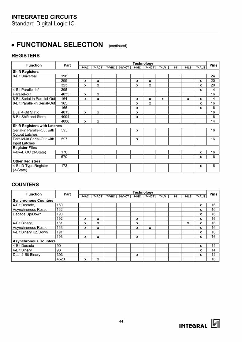
INTEGRATED CIRCUITS Standard Digital Logic IC
44
• FUNCTIONAL SELECTION (continued) REGISTERS
Function Part Technology Pins 74AC 74ACT 74VHC 74VHCT 74HC 74HCT 74LV 74 74LS 74ALS
Shift Registers 8-Bit Universal 198 24 299 x x x x x 20 323 x x x x x 20 4-Bit Parallel-in/ 295 x 14 Parallel-out 4035 x x 16 8-Bit Serial-in Parallel-Out 164 x x x x x x x 14 8-Bit Parallel-in Serial-Out 165 x x x 16 166 x x 16 Dual 4-Bit Static 4015 x х x 16 8-Bit Shift and Store 4094 x 16 4006 x x 14 Shift Registers with Latches Serial-in Parallel-Out with Output Latches
595 х 16
Parallel-in Serial-Out with Input Latches
597 x 16
Register Files 4-by-4, OC (3-State) 170 x 16 670 x 16 Other Registers 4-Bit D-Type Register (3-State)
173 x 16
COUNTERS
Function Part Technology Pins 74AC 74ACT 74VHC 74VHCT 74HC 74HCT 74LV 74 74LS 74ALSSynchronous Counters 4-Bit Decade, 160 x 16 Asynchronous Reset 162 x 16 Decade Up/Down 190 x 16 192 x x x x 16 4-Bit Binary, 161 x x х x x 16 Asynchronous Reset 163 x x х x x 16 4-Bit Binary Up/Down 191 x 16 193 x x х x 16 Asynchronous Counters 4-Bit Decade 90 х 14 4-Bit Binary 93 x 14 Dual 4-Bit Binary 393 x x 14 4520 x x 16
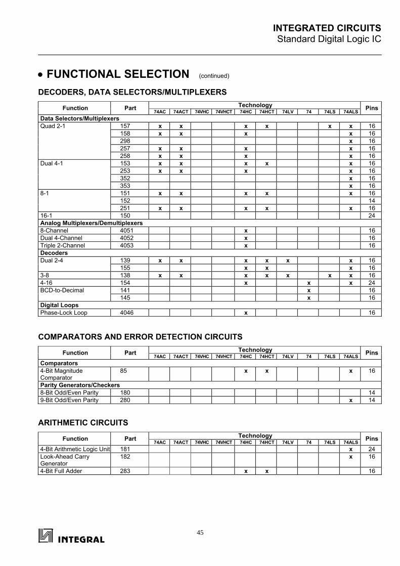
INTEGRATED CIRCUITS Standard Digital Logic IC
45
• FUNCTIONAL SELECTION (continued) DECODERS, DATA SELECTORS/MULTIPLEXERS
Function Part Technology Pins 74AC 74ACT 74VHC 74VHCT 74HC 74HCT 74LV 74 74LS 74ALS
Data Selectors/Multiplexers Quad 2-1 157 x x x x x x 16 158 x x x x 16 298 x 16 257 x x x x 16 258 x x x x 16 Dual 4-1 153 x x x x x 16 253 x x x x 16 352 x 16 353 x 16 8-1 151 x x x x x 16 152 14 251 x x x x x 16 16-1 150 24 Analog Multiplexers/Demultiplexers 8-Channel 4051 x 16 Dual 4-Channel 4052 x 16 Triple 2-Channel 4053 x 16 Decoders Dual 2-4 139 x x x x x x 16 155 x x x 16 3-8 138 x x x x x x x 16 4-16 154 x x x 24 BCD-to-Decimal 141 x 16 145 x 16 Digital Loops Phase-Lock Loop 4046 x 16
COMPARATORS AND ERROR DETECTION CIRCUITS
Function Part Technology Pins 74AC 74ACT 74VHC 74VHCT 74HC 74HCT 74LV 74 74LS 74ALS
Comparators 4-Bit Magnitude Comparator
85 x x x 16
Parity Generators/Checkers 8-Bit Odd/Even Parity 180 14 9-Bit Odd/Even Parity 280 x 14
ARITHMETIC CIRCUITS
Function Part Technology Pins 74AC 74ACT 74VHC 74VHCT 74HC 74HCT 74LV 74 74LS 74ALS4-Bit Arithmetic Logic Unit 181 x 24 Look-Ahead Carry Generator
182 x 16
4-Bit Full Adder 283 x x 16
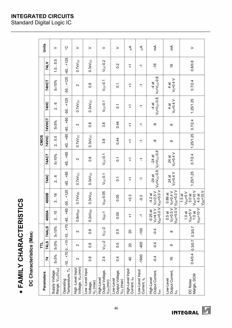
INTEGRATED CIRCUITS Standard Digital Logic IC
46
• FA
MIL
Y C
HA
RA
CTE
RIS
TIC
S
DC
Cha
ract
eris
tics
(Max
)
Uni
ts
V
°C
V
V
V
V
μA
μA
mA
mA
V
CM
OS
74LV
1.0…
5.5
-40…
+125
0.7х
VC
C
0.3х
VC
C
VC
C-0
.2
0.2
+1
-1
-16
16
0.8/
0.8
74H
CT
5±10
%
-55…
+125
2 0.8
VC
C-0
.1
0.1
+1
-1
-4 a
t V
0=V
CC-0
.8
4 at
V
0=0.
4 V
0.7/
2.4
74H
C
2…6
-55…
+125
0.7х
VC
C
0.3х
VC
C
VC
C-0
.1
0.1
+1
-1
-4 a
t V
0=V
CC-0
.8
4 at
V
0=0.
4 V
1.25
/1.2
5
74VH
CT
5±5%
-40…
+85
2 0.8
3.8
0.44
+1
-1
-8
8
0.7/
2.4
74VH
C
2…5.
5
-40…
+85
0.7х
VC
C
0.3х
VC
C
3.8
0.44
+1
-1
-8
8
1.25
/1.2
5
74A
CT
5±10
%
-45…
+85
2 0.8
VC
C-0
.1
0.1
+1
-1
-24
at
V0=
VC
C-0
.8
24 a
t V
0=0.
4 V
0.7/
2.4
74A
C
2…6
-45…
+85
0.7х
VC
C
0.3х
VC
C
VC
C-0
.1
0.1
+1
-1
-24
at
V0=
VC
C-0
.8
24 a
t V
0=0.
4 V
1.25
/1.2
5
4000
B
3…18
-55…
+125
0.7х
VD
D
0.3х
VD
D
VD
D-0
.05
0.05
+0.3
-0.3
-4.2
at
V0=
2.5
V
VD
D=5
.0 V
0.88
at
V0=
0.4
V
VD
D=5
.0 V
1.5
at
VD
D=5
V
3.0
at
VD
D=1
0 V
4.
0 at
V
DD=1
5 V
4000
A
3…15
-45…
+85
0.8х
VD
D
0.2х
VD
D
VD
D-1
0.05
+1
-1
-0.2
5 at
V
0=4.
5 V
V
DD=5
.0 V
0.5
at
V0=
0.5
V
VD
D=5
.0 V
1.0
at
VD
D=5
V
1.0
at
VD
D=1
0 V
TTL
74A
LS
5±10
%
-10…
+70
2 0.8
VC
C-2
0.5
20
-100
-0.4
8
0.3/
0.7
74LS
5±5%
0…+7
0
2 0.8
VC
C-2
0.5
20
-400
-0.4
8
0.3/
0.7
74
5±5%
-10…
+70
2 0.8
2.4
0.4
40
-160
0
-0.4
16
0.4/
0.4
Para
met
ers
Sup
ply
Vol
tage
R
ange
, VC
C(V
DD)
Ope
ratin
g Te
mpe
ratu
re, T
A
Hig
h -L
evel
Inpu
t V
olta
ge, V
IH (m
in)
Low
-Lev
el In
put
Vol
tage
, V
IL (m
ax)
Hig
h-Le
vel
Out
put V
olta
ge,
VO
H (m
in)
Low
-Lev
el
Out
put V
olta
ge,
VO
L (m
ax)
Hig
h-Le
vel I
nput
C
urre
nt, I
IH
Low
-Lev
el In
put
Cur
rent
, IIL
Hig
h-Le
vel
Out
put C
urre
nt,
I OH
Low
-Lev
el
Out
put C
urre
nt,
I OL
DC
Noi
se
Mar
gin,
DC
M
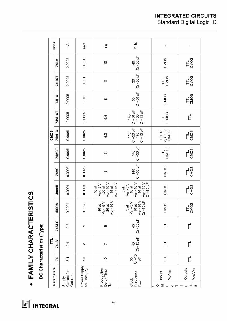
INTEGRATED CIRCUITS Standard Digital Logic IC
47
• F
AM
ILY
CH
AR
AC
TER
ISTI
CS
D
C C
hara
cter
istic
s (T
ype)
Uni
ts
mA
mW
ns
МH
z
- -
CM
OS
74LV
0.00
05
0.00
1
10
40
CL=
50 p
F
CM
OS
TTL,
C
MO
S
74H
CT
0.00
05
0.00
1
8 30
CL=
50 p
F
TTL,
C
MO
S
TTL,
C
MO
S
74H
C
0.00
05
0.00
1
8 30
CL=
50 p
F
CM
OS
TTL,
C
MO
S
74VH
CT
0.00
05
0.00
25
5.5
140
CL=
50 p
F 16
0 C
L=15
pF
TTL,
C
MO
S
TTL
74VH
C
0.00
05
0.00
25
5.3
115
CL=
50 p
F 17
0 C
L=15
pF
TTL
at
VO=3
.3V
, C
MO
S
TTL,
C
MO
S
74A
CT
0.00
05
0.00
25
5 140
CL=
50 p
F
TTL,
C
MO
S
TTL,
C
MO
S
74A
C
0.00
05
0.00
25
5 140
CL=
50 p
F
CM
OS
TTL,
C
MO
S
4000
B
0.00
01
0.00
01
40 a
t V
DD=5
V
20 a
t V
DD=1
0 V
15
at
VD
D=1
5 V
5 at
V
DD=5
V
10 a
t V
DD=1
0 V
14
at
VD
D=1
5 V
C
L=50
pF
CM
OS
TTL,
C
MO
S
4000
A
0.00
04
0.00
25
40 a
t V
DD=5
V
20 a
t V
DD=1
0 V
5 at
V
DD=5
V
10 a
t V
DD=1
0 V
C
L=15
pF
CM
OS
TTL,
C
MO
S
TTL
74A
LS
0.2 1 5 45
CL=
50 p
F
TTL
TTL
74LS
0.4 2 7 40
CL=
15 p
F
TTL
TTL
74
3.4
10
10
35
CL=
15
pF
TTL
TTL
Para
met
ers
Supp
ly
Cur
rent
for
Gat
e, I G
Pow
er S
uppl
y fo
r Gat
e, P
G
Prop
agat
ion
Del
ay T
ime,
T P
Clo
ck
Freq
uenc
y,
F max
Inpu
ts
VIL
/VIH
Out
puts
V
OL/V
OH
C
O
M
P
A
T I B
L
E
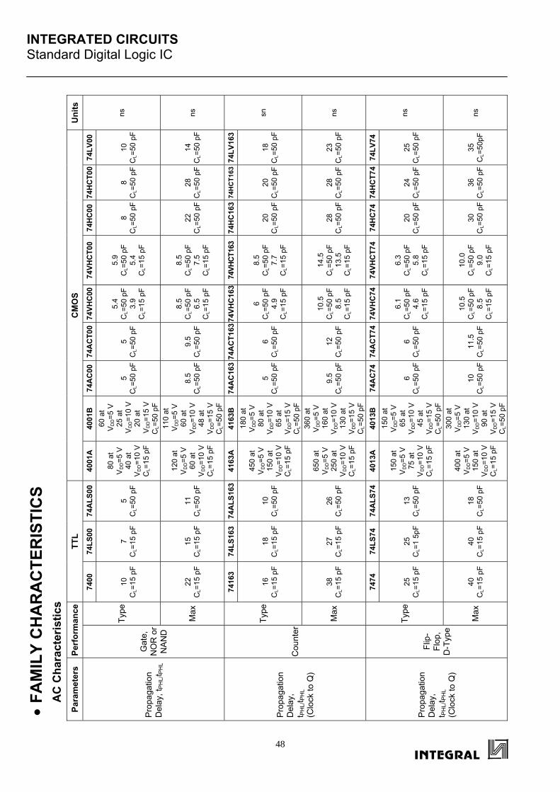
INTEGRATED CIRCUITS Standard Digital Logic IC
48
• FA
MIL
Y C
HA
RA
CTE
RIS
TIC
S
A
C C
hara
cter
istic
s
Uni
ts
ns
ns
sn
ns
ns
ns
CM
OS
74LV
00
10
CL=
50 p
F
14
CL=
50 p
F
74LV
163
18
CL=
50 p
F
23
CL=
50 p
F
74LV
74
25
CL=
50 p
F
35
CL=
50pF
74H
CT0
0
8 C
L=50
pF
28
CL=
50 p
F
74H
CT1
63
20
CL=
50 p
F
28
CL=
50 p
F
74H
CT7
4
24
CL=
50 p
F
36
CL=
50 p
F
74H
C00
8 C
L=50
pF
22
CL=
50 p
F
74H
C16
3
20
CL=
50 p
F
28
CL=
50 p
F
74H
C74
20
CL=
50 p
F
30
CL=
50 p
F
74VH
CT0
0
5.9
CL=
50 p
F 5.
4 C
L=15
pF
8.5
CL=
50 p
F 7.
5 C
L=15
pF
74VH
CT16
3
8.5
CL=
50 p
F 7.
7 C
L=15
pF
14.5
C
L=50
pF
13.5
C
L=15
pF
74VH
CT7
4
6.3
CL=
50 p
F 5.
8 C
L=15
pF
10.0
C
L=50
pF
9.0
CL=
15 p
F
74VH
C00
5.4
CL=
50 p
F 3.
9 C
L=15
pF
8.5
CL=
50 p
F 6.
5 C
L=15
pF
74VH
C16
3
6 C
L=50
pF
4.9
CL=
15 p
F
10.5
C
L=50
pF
8.5
CL=
15 p
F
74VH
C74
6.1
CL=
50 p
F 4.
6 C
L=15
pF
10.5
C
L=50
pF
8.5
CL=
15 p
F
74A
CT0
0
5 C
L=50
pF
9.5
CL=
50 p
F
74A
CT1
63
6 C
L=50
pF
12
CL=
50 p
F
74A
CT7
4
6 C
L=50
pF
11.5
C
L=50
pF
74A
C00
5 C
L=50
pF
8.5
CL=
50 p
F
74A
C16
3
5 C
L=50
pF
9.5
C
L=50
pF
74A
C74
6 C
L=50
pF
10
CL=
50 p
F
4001
B
60 a
t V
DD=5
V
25 a
t V
DD=1
0 V
20
at
VD
D=1
5 V
C
L=50
pF
110
at
VD
D=5
V
60 a
t V
DD=1
0 V
48
at
VD
D=1
5 V
C
L=50
pF
4163
B
180
at
VD
D=5
V
80 a
t V
DD=1
0 V
65
at
VD
D=1
5 V
C
L=50
pF
360
at
VD
D=5
V
160
at
VD
D=1
0 V
13
0 at
V
DD=1
5 V
C
L=50
pF
40
13B
15
0 at
V
DD=5
V
65 a
t V
DD=1
0 V
45
at
VD
D=1
5 V
C
L=50
pF
300
at
VD
D=5
V
130
at
VD
D=1
0 V
90
at
VD
D=1
5 V
C
L=50
pF
4001
A
80 a
t V
DD=5
V
40 a
t V
DD=1
0 V
C
L=15
pF
120
at
VD
D=5
V
60 a
t V
DD=1
0 V
C
L=15
pF
4163
A
450
at
VD
D=5
V
150
at
VD
D=1
0 V
C
L=15
pF
650
at
VD
D=5
V
250
at
VD
D=1
0 V
C
L=15
pF
4013
A
150
at
VD
D=5
V
75 a
t V
DD=1
0 V
C
L=15
pF
400
at
VD
D=5
V
150
at
VD
D=1
0 V
C
L=15
pF
TTL
74A
LS00
5 C
L=50
pF
11
CL=
50 p
F
74A
LS16
3
10
CL=
50 p
F
26
CL=
50 p
F
74A
LS74
13
CL=
50 p
F
18
CL=
50 p
F
74LS
00
7 C
L=15
pF
15
CL=
15 p
F
74LS
163
18
CL=
15 p
F
27
CL=
15 p
F
74LS
74
25
CL=
1 5p
F
40
CL=
15 p
F
7400
10
CL=
15 p
F
22
CL=
15 p
F
7416
3
16
CL=
15 p
F
38
CL=
15 p
F
7474
25
CL=
15 p
F
40
CL=
15 p
F
Perf
orm
ance
Type
Max
Type
Max
Type
Max
Gat
e,
NO
R o
r N
AND
Cou
nter
Flip
-Fl
op,
D-T
ype
Para
met
ers
Prop
agat
ion
Del
ay, t
PH
L/t P
HL
Prop
agat
ion
Del
ay,
t PH
L/t P
HL
(Clo
ck to
Q)
Prop
agat
ion
Del
ay,
t PH
L/t P
HL
(Clo
ck to
Q)
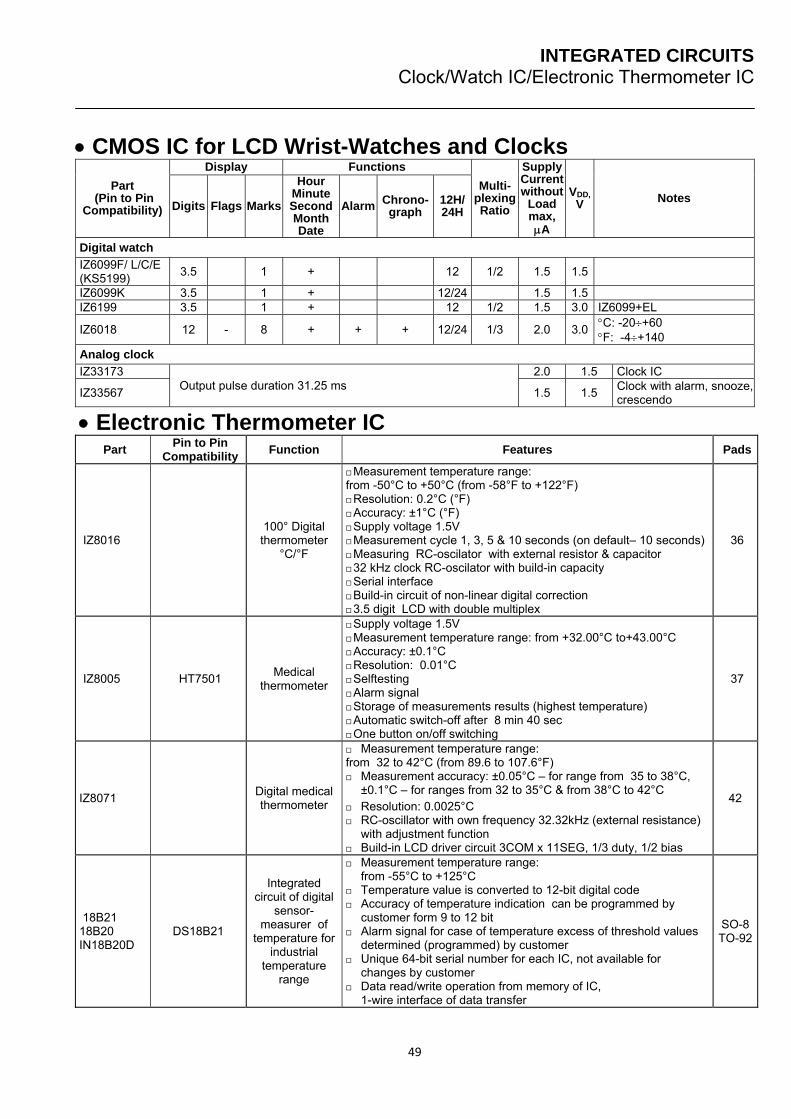
INTEGRATED CIRCUITS Clock/Watch IC/Electronic Thermometer IC
49
• CMOS IC for LCD Wrist-Watches and Clocks Part
(Pin to Pin Compatibility)
Display Functions Multi-
plexingRatio
Supply Current without
Load max, μA
VDD, V Notes Digits Flags Marks
Hour Minute SecondMonth Date
Alarm Chrono-graph
12H/24H
Digital watch IZ6099F/ L/C/E (KS5199) 3.5 1 + 12 1/2 1.5 1.5
IZ6099K 3.5 1 + 12/24 1.5 1.5 IZ6199 3.5 1 + 12 1/2 1.5 3.0 IZ6099+EL
IZ6018 12 - 8 + + + 12/24 1/3 2.0 3.0 °C: -20÷+60 °F: -4÷+140
Analog clock IZ33173
Output pulse duration 31.25 ms 2.0 1.5 Clock IC
IZ33567 1.5 1.5 Clock with alarm, snooze, crescendo
• Electronic Thermometer IC Part Pin to Pin
Compatibility Function Features Pads
IZ8016 100° Digital thermometer
°С/°F
Measurement temperature range: from -50°C to +50°C (from -58°F to +122°F)
Resolution: 0.2°C (°F) Accuracy: ±1°C (°F) Supply voltage 1.5V Measurement cycle 1, 3, 5 & 10 seconds (on default– 10 seconds) Measuring RC-oscilator with external resistor & capacitor 32 kHz clock RC-oscilator with build-in capacity Serial interface Build-in circuit of non-linear digital correction 3.5 digit LCD with double multiplex
36
IZ8005 HT7501 Medical thermometer
Supply voltage 1.5V Measurement temperature range: from +32.00°C to+43.00°C Accuracy: ±0.1°C Resolution: 0.01°C Selftesting Alarm signal Storage of measurements results (highest temperature) Automatic switch-off after 8 min 40 sec One button on/off switching
37
IZ8071 Digital medical thermometer
Measurement temperature range: from 32 to 42°C (from 89.6 to 107.6°F)
Measurement accuracy: ±0.05°C – for range from 35 to 38°C, ±0.1°C – for ranges from 32 to 35°C & from 38°C to 42°C
Resolution: 0.0025°C RC-oscillator with own frequency 32.32kHz (external resistance)
with adjustment function Build-in LCD driver circuit 3COM x 11SEG, 1/3 duty, 1/2 bias
42
18B21 18B20 IN18B20D
DS18B21
Integrated circuit of digital
sensor-measurer of
temperature for industrial
temperature range
Measurement temperature range: from -55°C to +125°C
Temperature value is converted to 12-bit digital code Accuracy of temperature indication can be programmed by
customer form 9 to 12 bit Alarm signal for case of temperature excess of threshold values
determined (programmed) by customer Unique 64-bit serial number for each IC, not available for
changes by customer Data read/write operation from memory of IC,
1-wire interface of data transfer
SO-8 ТО-92
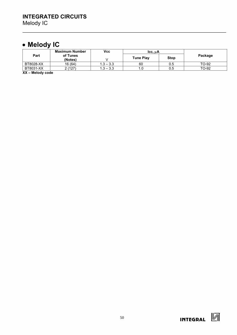
INTEGRATED CIRCUITS Melody IC
50
• Melody IC
Part Maximum Number
of Tunes (Notes)
Vcc
V
Icc, μA Package Tune Play Stop
ВТ8028-ХХ 16 (64) 1.3 – 3.3 60 0.5 TO-92 ВТ8031-ХХ 2 (127) 1.3 – 3.3 1.0 0.5 TO-92
ХХ – Melody code
DISCRETE SEMICONDUCTORS
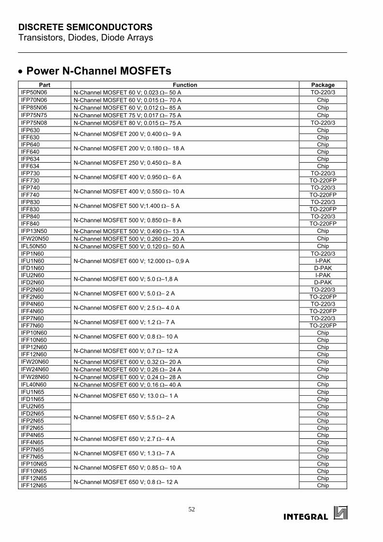
DISCRETE SEMICONDUCTORS Transistors, Diodes, Diode Arrays
52
• Power N-Channel MOSFETs Part Function Package
IFP50N06 N-Channel MOSFET 60 V; 0.023 Ω– 50 A TO-220/3 IFP70N06 N-Channel MOSFET 60 V; 0.015 Ω– 70 A Chip IFP85N06 N-Channel MOSFET 60 V; 0.012 Ω– 85 A Chip IFP75N75 N-Channel MOSFET 75 V; 0.017 Ω– 75 A Chip IFP75N08 N-Channel MOSFET 80 V; 0.015 Ω– 75 A TO-220/3 IFP630 N-Channel MOSFET 200 V; 0.400 Ω– 9 A ChipIFF630 ChipIFP640 N-Channel MOSFET 200 V; 0.180 Ω– 18 A ChipIFF640 ChipIFP634 N-Channel MOSFET 250 V; 0.450 Ω– 8 A ChipIFF634 ChipIFP730 N-Channel MOSFET 400 V; 0.950 Ω– 6 A TO-220/3 IFF730 TO-220FP IFP740 N-Channel MOSFET 400 V; 0.550 Ω– 10 A TO-220/3 IFF740 TO-220FP IFP830 N-Channel MOSFET 500 V;1.400 Ω– 5 A TO-220/3 IFF830 TO-220FP IFP840 N-Channel MOSFET 500 V; 0.850 Ω– 8 A TO-220/3 IFF840 TO-220FP IFP13N50 N-Channel MOSFET 500 V; 0.490 Ω– 13 A ChipIFW20N50 N-Channel MOSFET 500 V; 0.260 Ω– 20 A ChipIFL50N50 N-Channel MOSFET 500 V; 0.120 Ω– 50 A ChipIFP1N60
N-Channel MOSFET 600 V; 12.000 Ω– 0,9 A TO-220/3
IFU1N60 I-PAK IFD1N60 D-PAK IFU2N60 N-Channel MOSFET 600 V; 5.0 Ω–1,8 A I-PAK IFD2N60 D-PAK IFP2N60 N-Channel MOSFET 600 V; 5.0 Ω– 2 A TO-220/3 IFF2N60 TO-220FP IFP4N60 N-Channel MOSFET 600 V; 2.5 Ω– 4.0 A TO-220/3 IFF4N60 TO-220FP IFP7N60 N-Channel MOSFET 600 V; 1.2 Ω– 7 A TO-220/3 IFF7N60 TO-220FP IFP10N60 N-Channel MOSFET 600 V; 0.8 Ω– 10 A ChipIFF10N60 ChipIFP12N60 N-Channel MOSFET 600 V; 0.7 Ω– 12 A ChipIFF12N60 ChipIFW20N60 N-Channel MOSFET 600 V; 0.32 Ω– 20 A ChipIFW24N60 N-Channel MOSFET 600 V; 0.26 Ω– 24 A ChipIFW28N60 N-Channel MOSFET 600 V; 0.24 Ω– 28 A ChipIFL40N60 N-Channel MOSFET 600 V; 0.16 Ω– 40 A ChipIFU1N65 N-Channel MOSFET 650 V; 13.0 Ω– 1 A ChipIFD1N65 ChipIFU2N65
N-Channel MOSFET 650 V; 5.5 Ω– 2 A
ChipIFD2N65 ChipIFP2N65 ChipIFF2N65 ChipIFP4N65 N-Channel MOSFET 650 V; 2.7 Ω– 4 A ChipIFF4N65 ChipIFP7N65 N-Channel MOSFET 650 V; 1.3 Ω– 7 A ChipIFF7N65 ChipIFP10N65 N-Channel MOSFET 650 V; 0.85 Ω– 10 A ChipIFF10N65 ChipIFF12N65 N-Channel MOSFET 650 V; 0.8 Ω– 12 A ChipIFF12N65 Chip
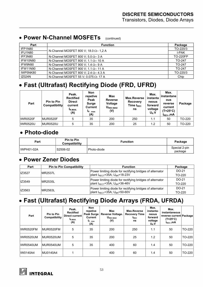
DISCRETE SEMICONDUCTORS Transistors, Diodes, Diode Arrays
53
• Power N-Channel MOSFETs (continued) Part Function Package
IFP1N80 N-Channel MOSFET 800 V; 18.0 Ω– 1,2 A TO-220/3 IFU1N80 I-PAK IFF3N80 N-Channel MOSFET 800 V; 5.0 Ω– 3 A TO-220FP IFW10N80 N-Channel MOSFET 800 V; 1.1 Ω– 10 A TO-247 IFW9N90 N-Channel MOSFET 900 V; 1.4 Ω– 9 A TO-247 IFW11N90 N-Channel MOSFET 900 V; 1.1 Ω– 11 A TO-247 IWP5NK80 N-Channel MOSFET 800 V; 2.4 Ω– 4.3 A TO-220/3 IZ024N N-Channel MOSFET 55 V; 0.075 Ω- 17 A Chip
• Fast (Ultrafast) Rectifying Diode (FRD, UFRD)
Part Pin to Pin Compatibility
Peak. Rectified
Direct current IR.MAX.
(А)
Non repetive
Peak Surge
Current IP. max
(A)
Max Reverse Voltage UREV.MAX
(V)
Max.Reverse Recovery Time tREC
ns
Max. instantaneous
forward voltage
UR V
Max. instantane
ous reverse current
(Т=25°С) IREV.,mA
Package
IWR0520F MUR0520F 5 35 200 250 1.1 50 TO-220 IWR0520U MUR0520U 5 35 200 25 1.2 50 TO-220
• Photo-diode Part Pin to Pin
Compatibility Function Package
IWPH01-02A S2506-02 Photo-diode Special 2-pin package
• Power Zener Diodes Part Pin to Pin Compatibility Function Package
IZ3527 MR2537L Power limiting diode for rectifying bridges of alternator plant IRECT=35A; UBR=18-23V
DO-21 TO-220
IZ3549 MR2535L Power limiting diode for rectifying bridges of alternator plant IRECT=35A; UBR=36-46V
DO-21 TO-220
IZ3563 MR2563L Power limiting diode for rectifying bridges of alternator plant IRECT=35A; UBR=50-60V
DO-21 TO-220
• Fast (Ultrafast) Rectifying Diode Arrays (FRDA, UFRDA)
Part Pin to Pin Compatibility
Peak. Rectified
Direct current IR.MAX. (А)
Non repetive
Peak Surge Current
IP. max (A)
Max Reverse Voltage.
UREV.MAX (V)
Max.Reverse Recovery Time
tREC ns
Max. instanta-
neous forward voltage
UR V
Max. instantaneous reverse current
(Т=25°С) IREV.,mA
Package
IWR0520FM MUR0520FM 5 35 200 250 1.1 50 TO-220
IWR0520UM MUR0520UM 5 35 200 25 1.2 50 TO-220
IWR0540UM MUR0540UM 5 35 400 60 1.4 50 TO-220
IW0140A4 MU0140A4 1 400 60 1.4 50 TO-220
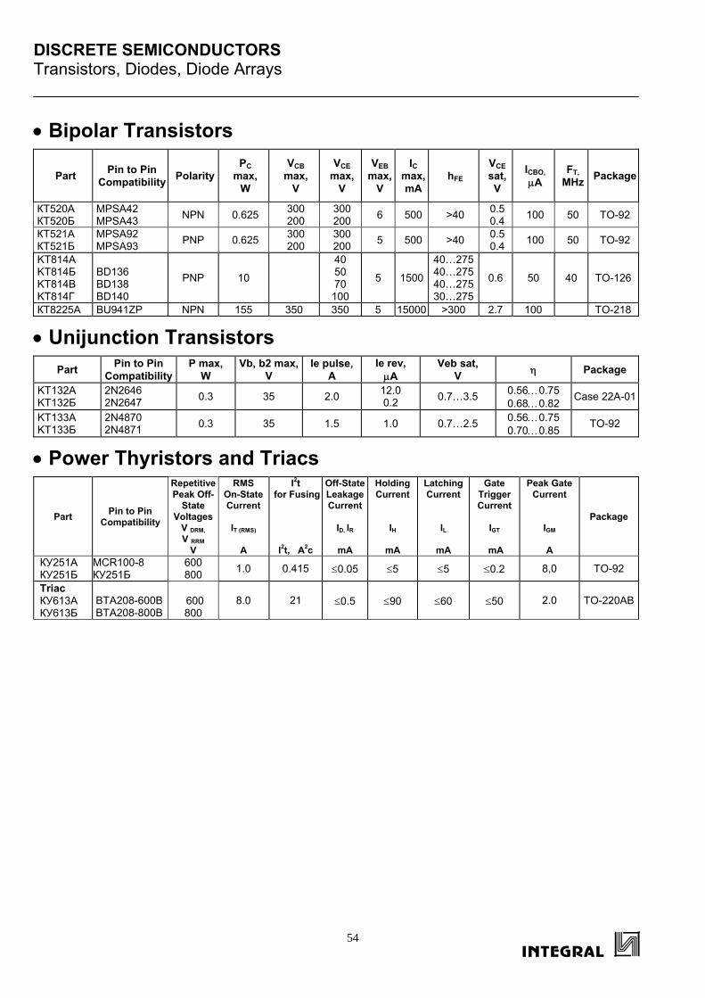
DISCRETE SEMICONDUCTORS Transistors, Diodes, Diode Arrays
54
• Bipolar Transistors
Part Pin to Pin Compatibility Polarity
РC max,
W
VCB max,
V
VCE max,
V
VEB max,
V
IC max,mА
hFE VCE sat, V
ICBO, μА
FT, МHz Package
КТ520А КТ520Б
MPSA42 MPSA43 NPN 0.625 300
200 300 200 6 500 >40 0.5
0.4 100 50 TO-92
КТ521А КТ521Б
MPSA92 MPSA93 PNP 0.625 300
200 300 200 5 500 >40 0.5
0.4 100 50 TO-92
KT814A KT814Б KT814B KT814Г
BD136 BD138 BD140
PNP 10
40 50 70
100
5 1500
40…27540…27540…27530…275
0.6 50 40 TO-126
КТ8225A BU941ZP NPN 155 350 350 5 15000 >300 2.7 100 TO-218
• Unijunction Transistors Part Pin to Pin
Compatibility P max,
W Vb, b2 max,
V Ie pulse,
A Ie rev, μA
Veb sat, V η Package
KT132A KT132Б
2N2646 2N2647 0.3 35 2.0 12.0
0.2 0.7…3.5 0.56…0.75 0.68…0.82 Case 22A-01
KT133A KT133Б
2N4870 2N4871 0.3 35 1.5 1.0 0.7…2.5 0.56…0.75
0.70…0.85 TO-92
• Power Thyristors and Triacs
Part Pin to Pin Compatibility
RepetitivePeak Off-
State Voltages
V DRM, V RRM
V
RMS On-State Current
IT (RMS)
А
I2t for Fusing
I2t, А2с
Off-State Leakage Current
ID, IR
mA
Holding Current
IH
mA
Latching Current
IL
mA
Gate Trigger Current
IGT
mA
Peak Gate Current
IGM А
Package
КУ251А КУ251Б
МСR100-8 КУ251Б
600 800 1.0 0.415 ≤0.05 ≤5 ≤5 ≤0.2 8,0 ТО-92
Triac КУ613А КУ613Б
BTA208-600B BTA208-800B
600 800
8.0
21 ≤0.5
≤90
≤60
≤50
2.0 TO-220AB

FOUNDRY - BUSINESS
55
Foundry business • Semiconductor IC and Discrete Devices Manufacturing under the Customer’s Design (delivery on base of Probe Test) • Semiconductor IC and Discrete Devices Manufacturing under the Customer’s Design (delivery on the base of PCM) • Wafer Fab Service – execution of separate Process Flow Steps or blocks (Metal sputtering, film deposition, EPI growing, back grinding,
wafers testing and so on) • Raw Si substrate and EPI manufacturing under the Customer’s Spec
Production Capacity available for Foundry Business: • 8’’ wafer production line (0.5-0.35μm design rule) • 6’’ wafer production line (0.8-1.2 μm design rule) • 4’’ wafer production line (1.2-3.0 μm design rule)
Basic Process available: a) Integrated Circuits: • DMOS • CMOS • BiCMOS • CDMOS • BiCDMOS • Bipolar
b) Discrete devices: • D-MOS (≤1000 V) • Multi-Epi (≤700 V) • Bipolar • Process for high frequency devices (≤300 V)
Si substrates and EPI, manufacturing and delivery (according to the Customer's Spec): • 3", 4", 6", 8’’ wafers • EPI parameter range: d=0.5...80 μm, ρ=0.1...50 Ω • cm
Mask making: • Mask Set manufacturing under the Customer’s Spec (GDS II and DB):
a) for contact lithography b) for Projection Reduction (Stepper lithography) (1:1/1:5/1:10)
• Pellicles manufacturing under the Customer’s Spec • Manufacture of photomasks with P/R coatings (glass and quartz substrates)
Contract management Packaging: • IC and Discrete Devices assembly (packaging) with Testing • IC and Discrete Devices assembly (packaging) without Testing • IC and Discrete Devices assembly (packaging) with Testing and Marking
Packages Types available: a) Integrated Circuits: • SOP (8-28 LD) • DIP (8-40 LD) • SHRINK DIP (30, 42, 52, 56 LD) • QFP (48, 64, 100 LD) • SIL (3, 8, 13, 17 LD) • SIP (9LD) • TO -220 (3, 5, 7 LD) • SOT -23, SOT -143, SОТ -223
b) Discrete devices: • Саsе 22А-01 • DO-34, DO-35 • МЕLF, miniMELF • SOT -23, SOT -143, SОТ -223 • ISOWATT • ТО-18, ТО-39, ТО-72, ТO-92, ТО-126, • ТО-218, ТО-220 • KD-17 • DРАК, D2РАК
Fabless service IC and discrete devices design: • IC Design according to the Customer’s Data Sheet (Spec) and Process Development • Discrete Devices Design according to the Customer’s Data Sheet (Spec) and Process development • GDS II and Tape out • Engineering Consulting service • Reengineering
Supplementary services
Design of electronic devices/ instruments and manufacture of samples as per Customer’s requirements: • Design and manufacture of PCB • Design and manufacture of LCD:
- TN-type (“twist”) for electronic clock/watch, calculators, etc, - STN-type (“supertwist”) for general purposes
Other services: • Design and manufacture of quartz tooling and accessories,
tools • Design and manufacture of molds, punches, casting/transfer
molds • Marking blocks manufacturing • High-precision stamping of lead frames for IC manufacturing
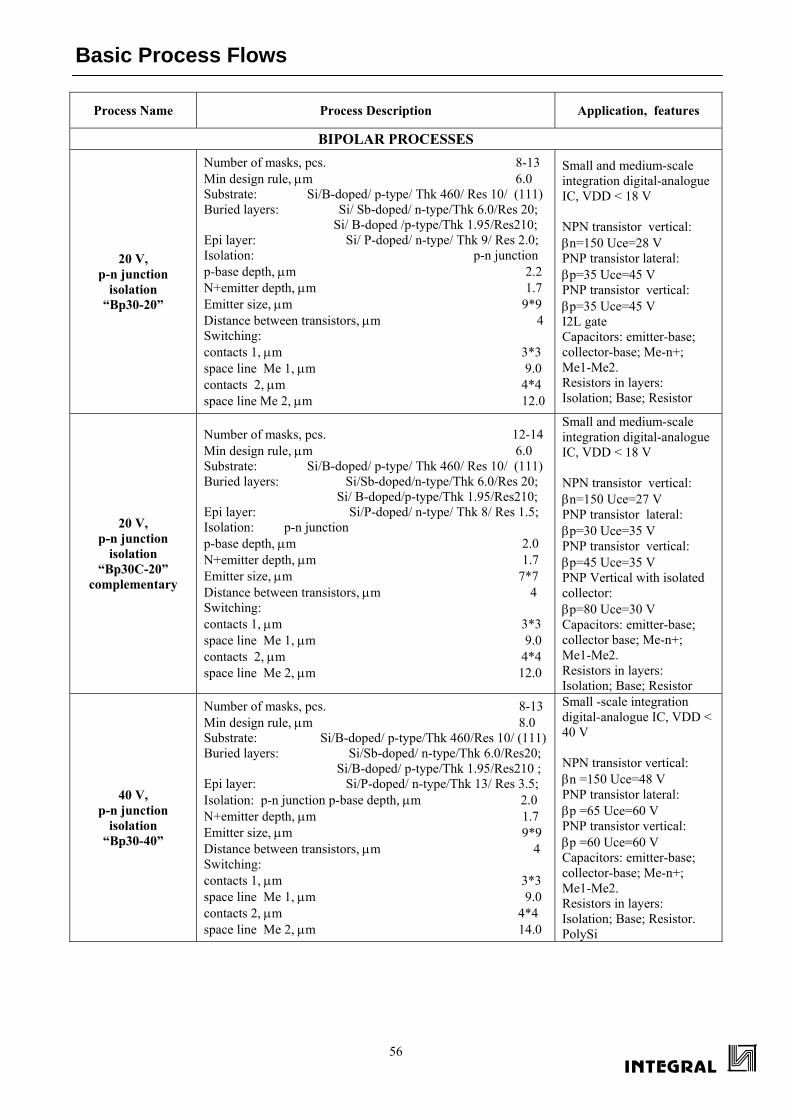
Basic Process Flows
56
Process Name Process Description Application, features
BIPOLAR PROCESSES
20 V, p-n junction
isolation “Bp30-20”
Number of masks, pcs. 8-13 Min design rule, μm 6.0 Substrate: Si/B-doped/ p-type/ Thk 460/ Res 10/ (111) Buried layers: Si/ Sb-doped/ n-type/Thk 6.0/Res 20; Si/ B-doped /p-type/Thk 1.95/Res210; Epi layer: Si/ P-doped/ n-type/ Thk 9/ Res 2.0; Isolation: p-n junction p-base depth, μm 2.2 N+emitter depth, μm 1.7 Emitter size, μm 9*9 Distance between transistors, μm 4 Switching: contacts 1, μm 3*3 space line Me 1, μm 9.0 contacts 2, μm 4*4 space line Me 2, μm 12.0
Small and medium-scale integration digital-analogue IC, VDD < 18 V NPN transistor vertical: βn=150 Uce=28 V РNP transistor lateral: βр=35 Uсе=45 V РNP transistor vertical: βр=35 Uсе=45 V I2L gate Capacitors: emitter-base; collector-base; Ме-n+; Ме1-Ме2. Resistors in layers: Isolation; Base; Resistor
20 V, p-n junction
isolation “Bp30С-20”
complementary
Number of masks, pcs. 12-14 Min design rule, μm 6.0 Substrate: Si/B-doped/ p-type/ Thk 460/ Res 10/ (111) Buried layers: Si/Sb-doped/n-type/Thk 6.0/Res 20; Si/ B-doped/p-type/Thk 1.95/Res210; Epi layer: Si/P-doped/ n-type/ Thk 8/ Res 1.5; Isolation: p-n junction p-base depth, μm 2.0 N+emitter depth, μm 1.7 Emitter size, μm 7*7 Distance between transistors, μm 4 Switching: contacts 1, μm 3*3 space line Me 1, μm 9.0 contacts 2, μm 4*4 space line Me 2, μm 12.0
Small and medium-scale integration digital-analogue IC, VDD < 18 V NPN transistor vertical: βn=150 Uce=27 V РNP transistor lateral: βр=30 Uсе=35 V РNP transistor vertical: βр=45 Uсе=35 V РNP Vertical with isolated collector: βр=80 Uсе=30 V Capacitors: emitter-base; collector base; Ме-n+; Ме1-Ме2. Resistors in layers: Isolation; Base; Resistor
40 V, p-n junction
isolation “Bp30-40”
Number of masks, pcs. 8-13 Min design rule, μm 8.0 Substrate: Si/B-doped/ p-type/Thk 460/Res 10/ (111) Buried layers: Si/Sb-doped/ n-type/Thk 6.0/Res20; Si/B-doped/ p-type/Thk 1.95/Res210 ; Epi layer: Si/P-doped/ n-type/Thk 13/ Res 3.5; Isolation: p-n junction p-base depth, μm 2.0 N+emitter depth, μm 1.7 Emitter size, μm 9*9 Distance between transistors, μm 4 Switching: contacts 1, μm 3*3 space line Me 1, μm 9.0 contacts 2, μm 4*4 space line Me 2, μm 14.0
Small -scale integration digital-analogue IC, VDD < 40 V NPN transistor vertical: βn =150 Uce=48 V РNP transistor lateral: βр =65 Uсе=60 V РNP transistor vertical: βр =60 Uсе=60 V Capacitors: emitter-base; collector-base; Ме-n+; Ме1-Ме2. Resistors in layers: Isolation; Base; Resistor. PolySi
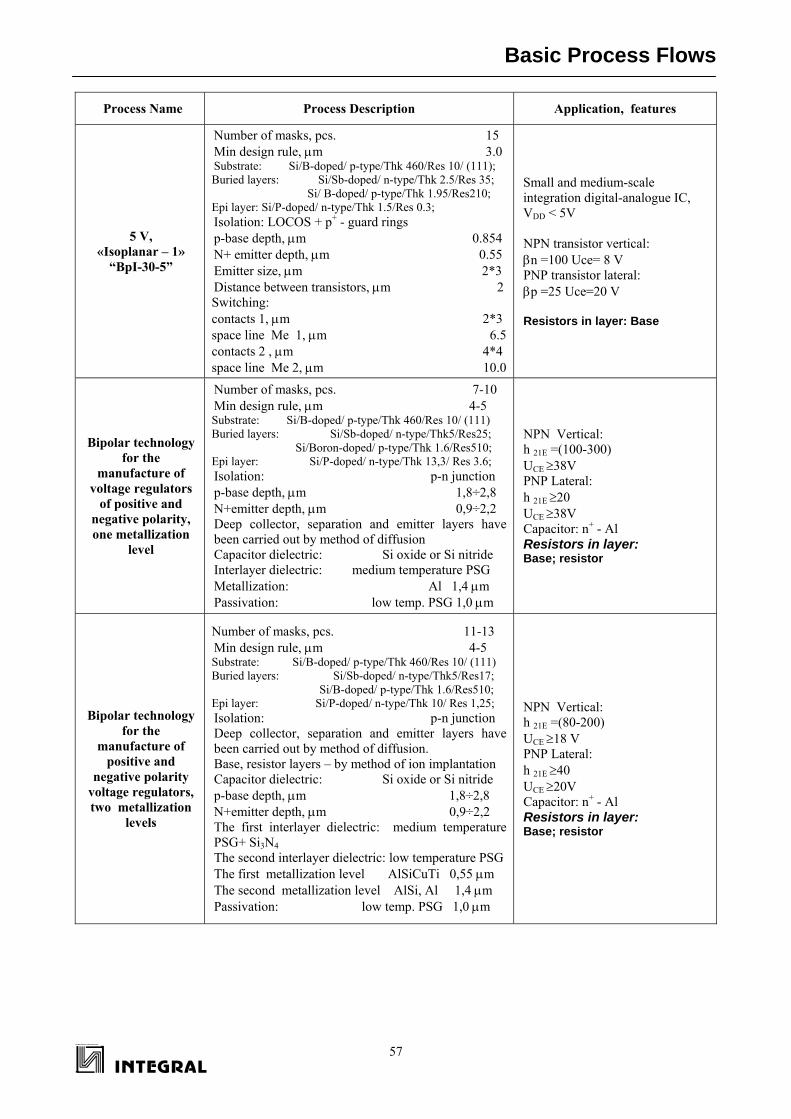
Basic Process Flows
57SEMICONDUCTOR DEVICES
Process Name Process Description Application, features
5 V, «Isoplanar – 1»
“BpI-30-5”
Number of masks, pcs. 15 Min design rule, μm 3.0 Substrate: Si/B-doped/ p-type/Thk 460/Res 10/ (111); Buried layers: Si/Sb-doped/ n-type/Thk 2.5/Res 35; Si/ B-doped/ p-type/Thk 1.95/Res210; Epi layer: Si/P-doped/ n-type/Thk 1.5/Res 0.3; Isolation: LOCOS + p+ - guard rings p-base depth, μm 0.854 N+ emitter depth, μm 0.55 Emitter size, μm 2*3 Distance between transistors, μm 2 Switching: contacts 1, μm 2*3 space line Me 1, μm 6.5 contacts 2 , μm 4*4 space line Me 2, μm 10.0
Small and medium-scale integration digital-analogue IC, VDD < 5V NPN transistor vertical: βn =100 Uсе= 8 V PNP transistor lateral: βр =25 Uce=20 V Resistors in layer: Base
Bipolar technology for the
manufacture of voltage regulators
of positive and negative polarity, one metallization
level
Number of masks, pcs. 7-10 Min design rule, μm 4-5 Substrate: Si/B-doped/ p-type/Thk 460/Res 10/ (111) Buried layers: Si/Sb-doped/ n-type/Thk5/Res25; Si/Boron-doped/ p-type/Thk 1.6/Res510; Epi layer: Si/P-doped/ n-type/Thk 13,3/ Res 3.6; Isolation: p-n junction p-base depth, μm 1,8÷2,8 N+emitter depth, μm 0,9÷2,2 Deep collector, separation and emitter layers have been carried out by method of diffusion Capacitor dielectric: Si oxide or Si nitride Interlayer dielectric: medium temperature PSG Metallization: Al 1,4 μm Passivation: low temp. PSG 1,0 μm
NPN Vertical: h 21E =(100-300) UCE ≥38V PNP Lateral: h 21E ≥20 UCE ≥38V Capacitor: n+ - Al Resistors in layer: Base; resistor
Bipolar technology for the
manufacture of positive and
negative polarity voltage regulators, two metallization
levels
Number of masks, pcs. 11-13 Min design rule, μm 4-5 Substrate: Si/B-doped/ p-type/Thk 460/Res 10/ (111) Buried layers: Si/Sb-doped/ n-type/Thk5/Res17; Si/B-doped/ p-type/Thk 1.6/Res510; Epi layer: Si/P-doped/ n-type/Thk 10/ Res 1,25; Isolation: p-n junction Deep collector, separation and emitter layers have been carried out by method of diffusion. Base, resistor layers – by method of ion implantation Capacitor dielectric: Si oxide or Si nitride p-base depth, μm 1,8÷2,8 N+emitter depth, μm 0,9÷2,2 The first interlayer dielectric: medium temperature PSG+ Si3N4 The second interlayer dielectric: low temperature PSG The first metallization level AlSiCuTi 0,55 μm The second metallization level AlSi, Al 1,4 μm Passivation: low temp. PSG 1,0 μm
NPN Vertical: h 21E =(80-200) UCE ≥18 V PNP Lateral: h 21E ≥40 UCE ≥20V Capacitor: n+ - Al Resistors in layer: Base; resistor
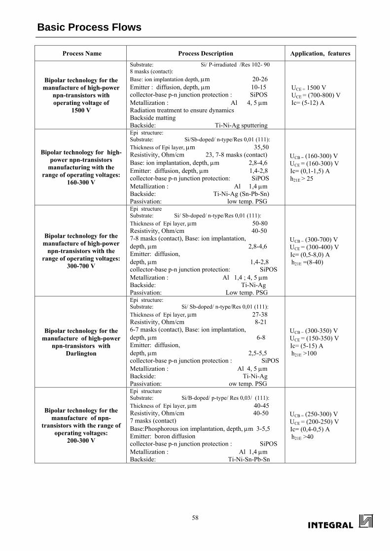
Basic Process Flows
58
Process Name Process Description Application, features
Bipolar technology for the manufacture of high-power
npn-transistors with operating voltage of
1500 V
Substrate: Si/ P-irradiated /Res 102- 90 8 masks (contact): Base: ion implantation depth, μm 20-26 Emitter : diffusion, depth, μm 10-15 collector-base p-n junction protection : SiPOS Metallization : Al 4, 5 μm Radiation treatment to ensure dynamics Backside matting Backside: Ti-Ni-Ag sputtering
UCE = 1500 V UCE = (700-800) V Ic= (5-12) A
Bipolar technology for high-power npn-transistors
manufacturing with the range of operating voltages:
160-300 V
Epi structure: Substrate: Si/Sb-doped/ n-type/Res 0,01 (111): Thickness of Epi layer, μm 35,50 Resistivity, Ohm/cm 23, 7-8 masks (contact) Base: ion implantation, depth, μm 2,8-4,6 Emitter: diffusion, depth, μm 1,4-2,8 collector-base p-n junction protection: SiPOS Metallization : Al 1,4 μm Backside: Ti-Ni-Ag (Sn-Pb-Sn) Passivation: low temp. PSG
UCB = (160-300) V UCE = (160-300) V Ic= (0,1-1,5) A h21E > 25
Bipolar technology for the manufacture of high-power
npn-transistors with the range of operating voltages:
300-700 V
Epi structure Substrate: Si/ Sb-doped/ n-type/Res 0,01 (111): Thickness of Epi layer, μm 50-80 Resistivity, Ohm/cm 40-50 7-8 masks (contact), Base: ion implantation, depth, μm 2,8-4,6 Emitter: diffusion, depth, μm 1,4-2,8 collector-base p-n junction protection: SiPOS Metallization : Al 1,4 ; 4, 5 μm Backside: Ti-Ni-Ag Passivation: Low temp. PSG
UCB = (300-700) V UCE = (300-400) V Ic= (0,5-8,0) A h21E =(8-40)
Bipolar technology for the manufacture of high-power
npn-transistors with Darlington
Epi structure: Substrate: Si/ Sb-doped/ n-type/Res 0,01 (111): Thickness of Epi layer, μm 27-38 Resistivity, Ohm/cm 8-21 6-7 masks (contact), Base: ion implantation, depth, μm 6-8 Emitter: diffusion, depth, μm 2,5-5,5 collector-base p-n junction protection : SiPOS Metallization : Al 4, 5 μm Backside: Ti-Ni-Ag Passivation: ow temp. PSG
UCB = (300-350) V UCE = (150-350) V Ic= (5-15) A h21E >100
Bipolar technology for the manufacture of npn-
transistors with the range of operating voltages:
200-300 V
Epi structure Substrate: Si/B-doped/ p-type/ Res 0,03/ (111): Thickness of Epi layer, μm 40-45 Resistivity, Ohm/cm 40-50 7 masks (contact) Base:Phosphorous ion implantation, depth, μm 3-5,5 Emitter: boron diffusion collector-base p-n junction protection : SiPOS Metallization : Al 1,4 μm Backside: Ti-Ni-Sn-Pb-Sn
UCB = (250-300) V UCE = (200-250) V Ic= (0,4-0,5) A h21E >40
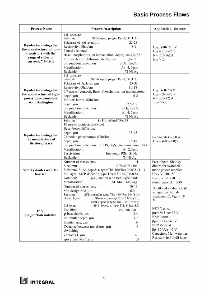
Basic Process Flows
59SEMICONDUCTOR DEVICES
Process Name Process Description Application, features
Bipolar technology for the manufacture of npn-
transistors with the range of collector current: 7,5÷16 A
Epi structure Substrate: Si/B-doped/ p-type/ Res 0,05/ (111): Thickness of Epi layer, μm 25-28 Resistivity, Ohm/cm 8-11 7 masks (contact) Base:Phosphorous ion implantation, depth, μm 4,5-7,5 Emitter: boron diffusion, depth, μm 1,4-2,5 p-n junction protection : SiO2, Ta2,O5 Metallization : Al 4, 0 μm Backside: Ti-Ni-Ag
UCB = (80-160) V UCE = (30-90) V Ic= (7,5-16) A h21E >15
Bipolar technology for the manufacture of high-
power npn-transistors with Darlington
Epi structure: Substrate: Si/ B-doped/ p-type/ Res 0,05/ (111): Thickness of the layer, μm 25-33 Resistivity, Ohm/cm 10-18 6,7 masks (contact), Base: Phosphorous ion implantation, depth, μm 6-8 Emitter: boron diffusion, depth, μm 2,5-5,5 p-n junction protection : SiO2, Ta2O5 Metallization : Al 4, 5 μm Backside: Ti-Ni-Ag
UCB = (60-70) V UCE = (60-70) V Ic= (2,0-12) A h21E >500
Bipolar technology for the manufacture of
tiristors, triacs
Substrate: Si/ P-irradiated / Res 35 10 masks (contact, two-side) Base: boron diffusion, depth, μm 35-45 Cathode : phosphorous diffusion, depth, μm 15-18 p-n junction protection: SiPOS, Si3N4, medium temp. PSG Metallization : Al 2,0 μm Passivation: low temp. PSG, Si3N4 Backside: Ti-Ni-Ag
IT (on-state) = 2,0 A Ubr = (600-800)V
Shottky diodes with Mo barrier
Number of masks, pcs. 4 Size, mm 0.76x0.76÷4x4 Substrate: Si/As-doped/ n-type/Thk 460/Res 0.0035 (111) Epi layer: Si/ P-doped/ n-type/Thk 4.5/Res (0.6-0.8) Isolation: p-n junction with field-type oxide Metallization: Al+Mo+Ti-Ni-Ag
Fast silicon Shottky diodes for switched mode power supplies Urev V 40-150 Irev. μa < 250 Idirect max. A 1-30
15 V, p-n junction isolation
Number of masks, pcs. 10-13 Min design rule, μm 6.0 Substrate: Si/B-doped/ p-type/ Thk 460/ Res 10/ (111) Buried layers: Si/Sb-doped/ n -type/Thk 6.0/Res 20; Si/B-doped/ p-type/Thk 1.95/Res210; Epi layer: Si/ P-doped/ n-type/ Thk 8/ Res 4.5; Isolation: p-n junction p-base depth, μm 2.4 N+emitter depth, μm 1.7 Emitter size, μm 6 Distance between transistors, μm 6 Switching: contacts 1, μm 4 space line Me 1, μm 13
Small and medium-scale integration digital-analogue IC, VDD < 18 V
NPN Vertical: βn=150 Uce=28 V РNP Lateral: βр=35 Uсе=45 V РNP Vertical: βр=35 Uсе=45 V Capacitor: Ме-n+emitter Resistors in PolySi layer

Basic Process Flows
60
Process Name Process Description Application, features
20 V, p-n junction isolation
Number of masks, pcs. 13 Min design rule, μm 6.0 Substrate: Si/B-doped/ p-type/ Thk 460/ Res 10/ (111) Buried layers: Si/Sb-doped/ n-type/Thk 5/Res 17; Si/B-doped/ p-type/Thk 1.6/Res510; Epi layer: Si/P-doped/ N-type/ Thk 10/ Res 1.25; Isolation: p-n junction p-base depth, μm 2.4 N+emitter depth, μm 1.7 Emitter size, μm 6 Distance between transistors, μm 6 Switching: contacts 1, μm 4 space line Me 1, μm 13.0 contacts 2, μm 4*4 space line Me 2, μm 12.0
Small and medium-scale integration digital-analogue IC, VDD < 18 V
NPN Vertical: βn=150 Uce=28 V РNP Lateral: βр=35 Uсе=45 V РNP Vertical: βр=35 Uсе=45 V I2L gate Capacitors: emitter-base; collector-base; Ме-n+; Ме1-Ме2. Resistors in layers: Isolation; Base; Resistor
CMOS PROCESSES
CMOS, 0.35 μm, 1 polySi, 2 metals, 200 mm
wafer
Number of photolithographies, pcs. 14 Design rule, μm 0.35 Substrate: 725KDB0,015(100) Epitaxial layer: 15KDB12 2 retrograde wells Interlayer dielectric: SACVD SiO2 + PC TEOS, μm 1.05 μm Gate SiO2, Å 120 Channel length NMOS/PMOS, μm 0.6 N&P LDD- drains Titanium silicide Metal I Ti/AlCu / Ti /TiN PolySi pitch, μm 1.0 Contacts 1 (W-filled), μm ø 0.5 Metal 1 pitch, μm 0.95 Metal 2 Ti/AlCu Contacts 2 (W-filled), μm ø 0.5 Metal 2 pitch, μm 1.2
Digital IC, highly-resistant, Epitaxy =5 V
NMOS: Vtn=0.6 V, Usd >7 V PMOS: Vtр=-0.6 V, Usd >7 V
CMOS, 0.35 μm, 1 polySi, 2 metals, 200 mm
wafer
Number of photolithographies, pcs. 15 Design rule, μm 0.35 Substrate: 725KDB0,015(100) Epitaxial layer: 15KDB12 2 retrograde wells Interlayer dielectric: SACVD SiO2 + PC TEOS, μm 1.05 μm Gate SiO2, Å 70 Channel length NMOS/PMOS, μm 0.35 N&P LDD- drains Titanium silicide Metal I Ti/AlCu / Ti /TiN PolySi pitch, μm 0.8 Contacts 1 (W-filled), μm ø 0.5 Metal 1 pitch, μm 0.95 Metal 2 Ti/AlCu Contacts 2 (W-filled), μm ø 0.5 Metal 2 pitch, μm 1.1
Digital IC, highly-resistant, Epitaxy = 3 V
NMOS: Vtn=0.6 V, Usd >5 V
PMOS: Vtр=-0.6 V, Usd >5 V
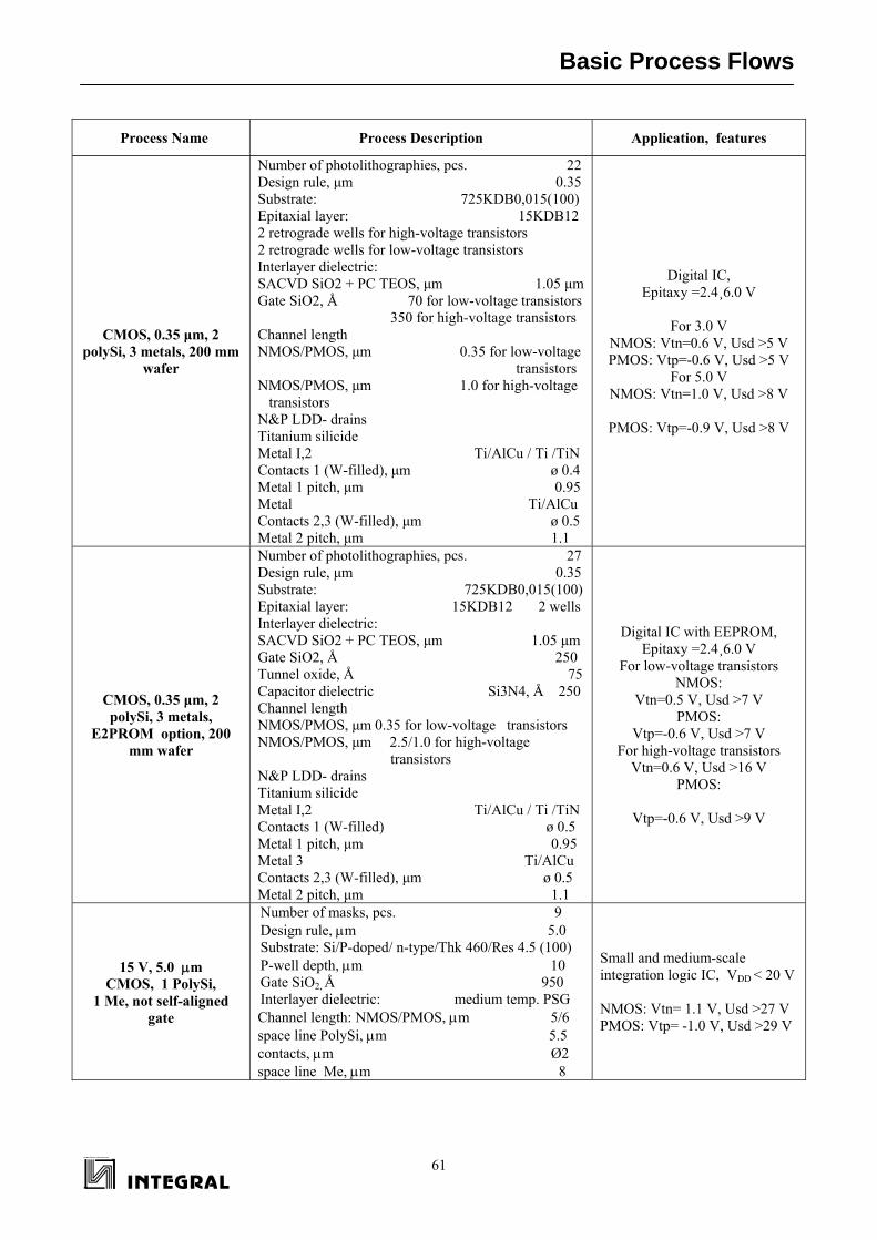
Basic Process Flows
61SEMICONDUCTOR DEVICES
Process Name Process Description Application, features
CMOS, 0.35 μm, 2 polySi, 3 metals, 200 mm
wafer
Number of photolithographies, pcs. 22 Design rule, μm 0.35 Substrate: 725KDB0,015(100) Epitaxial layer: 15KDB12 2 retrograde wells for high-voltage transistors 2 retrograde wells for low-voltage transistors Interlayer dielectric: SACVD SiO2 + PC TEOS, μm 1.05 μm Gate SiO2, Å 70 for low-voltage transistors 350 for high-voltage transistors Channel length NMOS/PMOS, μm 0.35 for low-voltage transistors NMOS/PMOS, μm 1.0 for high-voltage transistors N&P LDD- drains Titanium silicide Metal I,2 Ti/AlCu / Ti /TiN Contacts 1 (W-filled), μm ø 0.4 Metal 1 pitch, μm 0.95 Metal Ti/AlCu Contacts 2,3 (W-filled), μm ø 0.5 Metal 2 pitch, μm 1.1
Digital IC, Epitaxy =2.4¸6.0 V
For 3.0 V
NMOS: Vtn=0.6 V, Usd >5 V PMOS: Vtр=-0.6 V, Usd >5 V
For 5.0 V NMOS: Vtn=1.0 V, Usd >8 V
PMOS: Vtр=-0.9 V, Usd >8 V
CMOS, 0.35 μm, 2 polySi, 3 metals,
E2PROM option, 200 mm wafer
Number of photolithographies, pcs. 27 Design rule, μm 0.35 Substrate: 725KDB0,015(100) Epitaxial layer: 15KDB12 2 wells Interlayer dielectric: SACVD SiO2 + PC TEOS, μm 1.05 μm Gate SiO2, Å 250 Tunnel oxide, Å 75 Capacitor dielectric Si3N4, Å 250 Channel length NMOS/PMOS, μm 0.35 for low-voltage transistors NMOS/PMOS, μm 2.5/1.0 for high-voltage transistors N&P LDD- drains Titanium silicide Metal I,2 Ti/AlCu / Ti /TiN Contacts 1 (W-filled) ø 0.5 Metal 1 pitch, μm 0.95 Metal 3 Ti/AlCu Contacts 2,3 (W-filled), μm ø 0.5 Metal 2 pitch, μm 1.1
Digital IC with EEPROM, Epitaxy =2.4¸6.0 V
For low-voltage transistors NMOS:
Vtn=0.5 V, Usd >7 V PMOS:
Vtр=-0.6 V, Usd >7 V For high-voltage transistors
Vtn=0.6 V, Usd >16 V PMOS:
Vtр=-0.6 V, Usd >9 V
15 V, 5.0 μm CMOS, 1 PolySi,
1 Me, not self-aligned gate
Number of masks, pcs. 9 Design rule, μm 5.0 Substrate: Si/P-doped/ n-type/Thk 460/Res 4.5 (100) P-well depth, μm 10 Gate SiO2, Å 950 Interlayer dielectric: medium temp. PSG Channel length: NMOS/PMOS, μm 5/6 space line PolySi, μm 5.5 contacts, μm Ø2 space line Me, μm 8
Small and medium-scale integration logic IC, VDD < 20 V NMOS: Vtn= 1.1 V, Usd >27 V PMOS: Vtp= -1.0 V, Usd >29 V
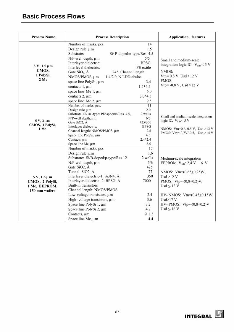
Basic Process Flows
62
Process Name Process Description Application, features
5 V, 1.5 μm CMOS, 1 PolySi,
2 Me
Number of masks, pcs. 14 Design rule, μm 1.5 Substrate: Si/ P-doped/n-type/Res 4.5 N/P-well depth, μm 5/5 Interlayer dielectric: BPSG Interlevel dielectric: PE oxide Gate SiO2, Å 245, Channel length: NMOS/PMOS, μm 1.4/2.0, N LDD-drains space line PolySi , μm 3.4 contacts 1, μm 1.5*4.5 space line Me 1, μm 6.0 contacts 2, μm 3.0*4.5 space line Me 2, μm 9.5
Small and medium-scale integration logic IC, VDD < 5 V
NMOS: Vtn= 0.8 V, Usd >12 V PMOS: Vtp= -0.8 V, Usd >12 V
5 V, 2 μm CMOS, 1 PolySi,
1 Me
Number of masks, pcs. 11 Design rule, μm 2.0 Substrate: Si/ /n -type/ Phosphorus/Res 4.5, 2 wells N/P-well depth, μm 6/7 Gate SiO2, Å 425/300 Interlayer dielectric: BPSG Channel length: NMOS/PMOS, μm 2.5 Space line PolySi, μm 4.5 Contacts, μm 2.4*2.4 Space line Me, μm 8.5
Small and medium-scale integration logic IC, VDD < 5 V NMOS: Vtn=0.6/ 0.5 V, Usd >12 V PMOS: Vtр=-0,7V/-0,5, Usd >14 V
5 V, 1.6 μm CMOS, 2 PolySi, 1 Me, EEPROM,
150 mm wafers
Number of masks, pcs. 17 Design rule, μm 1.6 Substrate: Si/B-doped/p-type/Res 12 2 wells N/P-well depth, μm 5/6 Gate SiO2, Å 425 Tunnel SiO2, Å 77 Interlayer dielectric-1: Si3N4, Å 350 Interlayer dielectric -2: BPSG, Å 7000 Built-in transistors Channel length: NMOS/PMOS Low-voltage transistors, μm 2.4 High- voltage transistors, μm 3.6 Space line PolySi 1, μm 3.2 Space line PolySi 2, μm 4.2 Contacts, μm Ø 1.2 Space line Me, μm 4.4
Medium-scale integration EEPROM, VDD: 2,4 V… 6 V NMOS: Vtn=(0,65+0,25)V, Usd ≥12 V PMOS: Vtр=-(0,8+0,2)V, Usd ≤-12 V HV- NMOS: Vtn=(0,45+0,15)V Usd≥17 V HV- РMOS: Vtр=-(0,8+0,2)V Usd ≤-16 V

Basic Process Flows
63SEMICONDUCTOR DEVICES
Process Name Process Description Application, features
5 V, 1.2 μm CMOS, 2 PolySi, 2 Me, low voltage EEPROM, 150 mm
wafers
Number of masks, pcs. 3 (marked) Design rule, μm 1.2 Substrate: Si/B-doped/ p-type/Res 12, 2 wells N/P-well depth, μm 5/6 Gate SiO2: Low voltage transistors, Å 250 High voltage transistors, Å 350 Tunnel SiO2, Å 77 Interlayer dielectric-1: Si3N4, Å 350 Interlayer dielectric -2: BPSG, Å 7000 Interlevel dielectric: PEoxide+SOG+ PEoxide Channel length: Low voltage NMOS/PMOS, μm 1.4/1.6 High voltage NMOS/PMOS, μm 2.6/2.6 N & P LDD- drains Built-in transistors Space line PolySi 1, μm 3.2 Space line PolySi 2, contact free, μm 2.4 Space line PolySi 2, with contact, μm 4,6 Contacts-1, μm Ø 1.2 Space line Me 1, contact free, μm 3.2 Space line Me 2, with contact, μm 4,4 Contacts 2, μm Ø 1.4 Space line Me 2, contact free, μm 4.4 Space line Me 2, with contact, μm 4,8
LSI EEPROM, VDD: 2,4 V… 6
V
LV NMOS: Vtn=(0.4-0,8)V, Usd≥12 V LV PMOS: Vtр=-(0.5-0,9)V, Usd ≤-12 V HV- NMOS: Vtn=(0,3-0,6)V, Usd≥17 V HV- РMOS: Vtр=-(0,6-1,0)V, Usd ≤-15 V
1.5 V, 1.6 μm CMOS, 1 PolySi,
1 Me, low threshold, 150mm wafers
Number of masks, pcs. 11 Design rule, μm 1.6 Substrate: Si/ B-doped/ p-type/Res 12 2 wells N/P-well depth, μm 5/6 Gate SiO2, Å 300 Interlayer dielectric – BPSG Channel length: NMOS/PMOS, μm 2.0 space line PolySi , μm 3.2 contacts, μm Ø 1.5 space line Me, μm 3.6
Medium-scale integration digital IC for electronic timepieces and micro calculators, VDD 1.5 V÷3 V. NMOS: Vtn= 0.5 V, Usd >10 V PMOS: Vtp= -0.5 V, Usd >10 V
5 V, 1.5 μm CMOS, 1 PolySi,
1 Me, 150mm wafers
Number of masks, pcs. 16 Design rule, μm 1.5 Substrate: Si/B-doped/ p-type/Res 12 2 wells N/P-well depth, μm 5/6 Interlayer dielectric: BPSG Gate SiO2, Å 250 Interlayer dielectric: BPSG, Transistor built in ROM, Buried contacts, Channel length: NMOS/PMOS, μm 1.5 N & P LDD- drains, space line PolySi, μm 2.5 contacts, μm Ø 1.5 space line Me, μm 3.5
Digital IMC, microcontrollers with VDD= 5V NMOS: Vtn= 0.6V, Usd >10 V PMOS: Vtp= 1.0V, Usd >13 V
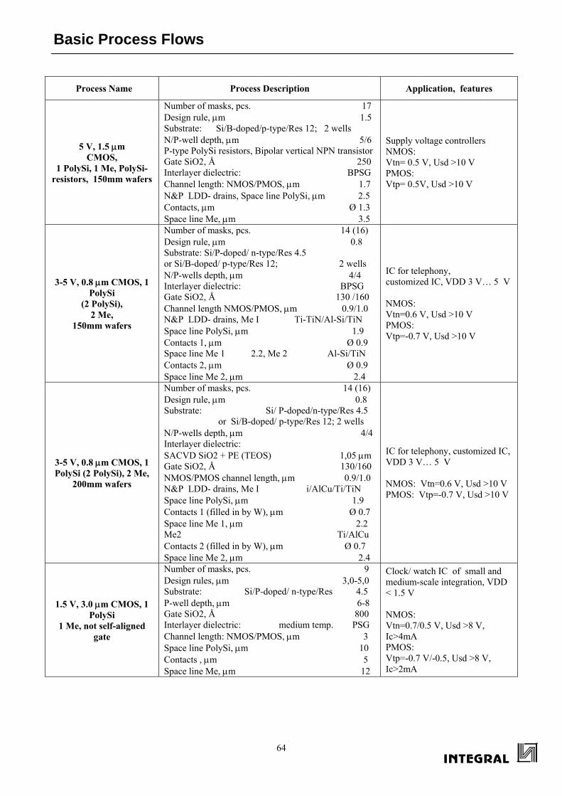
Basic Process Flows
64
Process Name Process Description Application, features
5 V, 1.5 μm CMOS,
1 PolySi, 1 Ме, PolySi- resistors, 150mm wafers
Number of masks, pcs. 17 Design rule, μm 1.5 Substrate: Si/B-doped/p-type/Res 12; 2 wells N/P-well depth, μm 5/6 P-type PolySi resistors, Bipolar vertical NPN transistor Gate SiO2, Å 250 Interlayer dielectric: BPSG Channel length: NMOS/PMOS, μm 1.7 N&P LDD- drains, Space line PolySi, μm 2.5 Contacts, μm Ø 1.3 Space line Me, μm 3.5
Supply voltage controllers NMOS: Vtn= 0.5 V, Usd >10 V PMOS: Vtp= 0.5V, Usd >10 V
3-5 V, 0.8 μm CMOS, 1 PolySi
(2 PolySi), 2 Me,
150mm wafers
Number of masks, pcs. 14 (16) Design rule, μm 0.8 Substrate: Si/P-doped/ n-type/Res 4.5 or Si/B-doped/ p-type/Res 12; 2 wells N/P-wells depth, μm 4/4 Interlayer dielectric: BPSG Gate SiO2, Å 130 /160 Channel length NMOS/PMOS, μm 0.9/1.0 N&P LDD- drains, Me I Ti-TiN/Al-Si/TiN Space line PolySi, μm 1.9 Contacts 1, μm Ø 0.9 Space line Me 1 2.2, Me 2 Al-Si/TiN Contacts 2, μm Ø 0.9 Space line Me 2, μm 2.4
IC for telephony, customized IC, VDD 3 V… 5 V NMOS: Vtn=0.6 V, Usd >10 V PMOS: Vtр=-0.7 V, Usd >10 V
3-5 V, 0.8 μm CMOS, 1 PolySi (2 PolySi), 2 Me,
200mm wafers
Number of masks, pcs. 14 (16) Design rule, μm 0.8 Substrate: Si/ P-doped/n-type/Res 4.5 or Si/B-doped/ p-type/Res 12; 2 wells N/P-wells depth, μm 4/4 Interlayer dielectric: SACVD SiO2 + PE (TEOS) 1,05 μm Gate SiO2, Å 130/160 NMOS/PMOS channel length, μm 0.9/1.0 N&P LDD- drains, Me I i/AlCu/Ti/TiN Space line PolySi, μm 1.9 Contacts 1 (filled in by W), μm Ø 0.7 Space line Me 1, μm 2.2 Me2 Ti/AlCu Contacts 2 (filled in by W), μm Ø 0.7 Space line Me 2, μm 2.4
IC for telephony, customized IC, VDD 3 V… 5 V NMOS: Vtn=0.6 V, Usd >10 V PMOS: Vtр=-0.7 V, Usd >10 V
1.5 V, 3.0 μm CMOS, 1 PolySi
1 Me, not self-aligned gate
Number of masks, pcs. 9 Design rules, μm 3,0-5,0 Substrate: Si/P-doped/ n-type/Res 4.5 P-well depth, μm 6-8 Gate SiO2, Å 800 Interlayer dielectric: medium temp. PSG Channel length: NMOS/PMOS, μm 3 Space line PolySi, μm 10 Contacts , μm 5 Space line Me, μm 12
Clock/ watch IC of small and medium-scale integration, VDD < 1.5 V NMOS: Vtn=0.7/0.5 V, Usd >8 V, Ic>4mA PMOS: Vtр=-0.7 V/-0.5, Usd >8 V, Ic>2mA
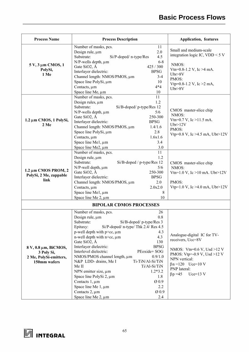
Basic Process Flows
65SEMICONDUCTOR DEVICES
Process Name Process Description Application, features
5 V, 3 μm CMOS, 1 PolySi, 1 Me
Number of masks, pcs. 11 Design rule, μm 2.0 Substrate: Si/P-doped/ n-type/Res 4.5 N/P-wells depth, μm 6-8 Gate SiO2, Å 425 / 300 Interlayer dielectric: BPSG Channel length: NMOS/PMOS, μm 3-4 Space line PolySi, μm 10 Contacts, μm 4*4 Space line Me, μm 10
Small and medium-scale integration logic IC, VDD < 5 V NMOS: Vtn=0.8-1.2 V, Ic >4 mA. Ubr>8V PMOS: Vtр=0.8-1.2 V, Ic >2 mA, Ubr>8V
1.2 μm CMOS, 1 PolySi, 2 Me
Number of masks, pcs. 11 Design rules, μm 1.2 Substrate: Si/B-doped/ p-type/Res 12 N/P-wells depth, μm 5/6 Gate SiO2, Å 250-300 Interlayer dielectric: BPSG Channel length: NMOS/PMOS, μm 1.4/1.6 Space line PolySi, μm 2.8 Contacts, μm 1.6x1.6 Space line Me1, μm 3.4 Space line Me2, μm 3.0
CMOS master-slice chip NMOS: Vtn=0.7 V, Ic >11.5 mA. Ubr>12V PMOS: Vtр=0.8 V, Ic >4.5 mA, Ubr>12V
1.2 μm CMOS PROM, 2 PolySi, 2 Me, zappable
link
Number of masks, pcs. 11 Design rule, μm 1.2 Substrate: Si/B-doped / p-type/Res 12 N/P-well depth, μm 5/6 Gate SiO2, Å 250-300 Interlayer dielectric: BPSG Channel length: NMOS/PMOS, μm 2.0 Contacts, μm 2.0x2.0 Space line Me1, μm 8 Space line Me 2, μm 10
CMOS master-slice chip NMOS: Vtn=1.0 V, Ic >10 mA. Ubr>12V PMOS: Vtр=1.0 V, Ic >4.0 mA, Ubr>12V
BIPOLAR CDMOS PROCESSES
8 V, 0.8 μm, BiCMOS, 3 Poly Si,
2 Me, PolySi-emitters, 150mm wafers
Number of masks, pcs. 26 Design rule, μm 0.8 Substrate: Si/B-doped/ p-type/Res 3 Epitaxy: Si/P-doped/ n-type/ Thk 2.4/ Res 4.5 p-well depth with p+cc, μm 4.3 n-well depth with n+cc, μm 4.3 Gate SiO2, Å 130 Interlayer dielectric: BPSG Interlevel dielectric: PEoxide+ SOG NMOS/PMOS channel length, μm 0.9/1.0 N&P LDD- drains, Me I Ti-TiN/Al-Si/TiN Me II Ti/Al-Si/TiN NPN emitter size, μm 1.2*3.2 Space line PolySi 2, μm 1.8 Contacts 1, μm Ø 0.9 Space line Me 1, μm 2.2 Contacts 2, μm Ø 0.9 Space line Me 2, μm 2.4
Analogue-digital IC for TV-receivers, Ucc=8V NMOS: Vtn=0.6 V, Usd >12 V PMOS: Vtр=-0.9 V, Usd >12 V NPN vertical: βn =120 Uce=10 V PNP lateral: βp =45 Uce=13 V
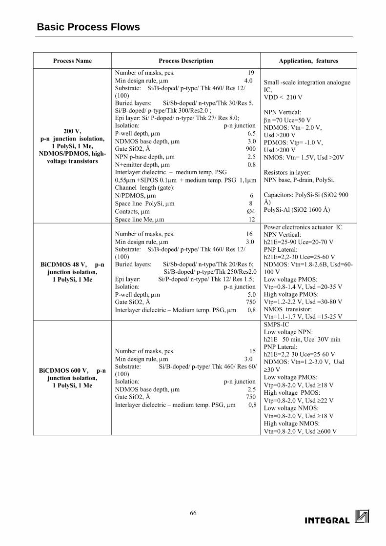
Basic Process Flows
66
Process Name Process Description Application, features
200 V, p-n junction isolation,
1 PolySi, 1 Me, NDMOS/PDMOS, high-
voltage transistors
Number of masks, pcs. 19 Min design rule, μm 4.0 Substrate: Si/B-doped/ p-type/ Thk 460/ Res 12/ (100) Buried layers: Si/Sb-doped/ n-type/Thk 30/Res 5. Si/B-doped/ p-type/Thk 300/Res2.0 ; Epi layer: Si/ P-doped/ n-type/ Thk 27/ Res 8.0; Isolation: p-n junction P-well depth, μm 6.5 NDMOS base depth, μm 3.0 Gate SiO2, Å 900 NPN p-base depth, μm 2.5 N+emitter depth, μm 0.8 Interlayer dielectric – medium temp. PSG 0,55μm +SIPOS 0.1μm + medium temp. PSG 1,1μm Channel length (gate): N/PDMOS, μm 6 Space line PolySi, μm 8 Contacts, μm Ø4 Space line Me, μm 12
Small -scale integration analogue IC, VDD < 210 V NPN Vertical: βn =70 Uсе=50 V NDMOS: Vtn= 2.0 V, Usd >200 V PDMOS: Vtp= -1.0 V, Usd >200 V NMOS: Vtn= 1.5V, Usd >20V Resistors in layer: NPN base, Р-drain, PolySi. Capacitors: PolySi-Si (SiO2 900 Å) PolySi-Al (SiO2 1600 Å)
BiCDMOS 48 V, p-n junction isolation,
1 PolySi, 1 Me
Number of masks, pcs. 16 Min design rule, μm 3.0 Substrate: Si/B-doped/ p-type/ Thk 460/ Res 12/ (100) Buried layers: Si/Sb-doped/ n-type/Thk 20/Res 6; Si/B-doped/ p-type/Thk 250/Res2.0 Epi layer: Si/P-doped/ n-type/ Thk 12/ Res 1.5; Isolation: p-n junction P-well depth, μm 5.0 Gate SiO2, Å 750 Interlayer dielectric – Medium temp. PSG, μm 0,8
Power electronics actuator IC NPN Vertical: h21E=25-90 Uсе=20-70 V PNP Lateral: h21E=2,2-30 Uсе=25-60 V NDMOS: Vtn=1.8-2.6В, Usd=60-100 V Low voltage PMOS: Vtp=0.8-1.4 V, Usd =20-35 V High voltage PMOS: Vtp=1.2-2.2 V, Usd =30-80 V NMOS transistor: Vtn=1.1-1.7 V, Usd =15-25 V
BiCDMOS 600 V, p-n junction isolation,
1 PolySi, 1 Me
Number of masks, pcs. 15 Min design rule, μm 3.0 Substrate: Si/B-doped/ p-type/ Thk 460/ Res 60/ (100) Isolation: p-n junction NDMOS base depth, μm 2.5 Gate SiO2, Å 750 Interlayer dielectric – medium temp. PSG, μm 0,8
SMPS-IC Low voltage NPN: h21E 50 min, Uсе 30V min PNP Lateral: h21E=2,2-30 Uсе=25-60 V NDMOS: Vtn=1.2-3.0 V, Usd ≥30 V Low voltage PMOS: Vtp=0.8-2.0 V, Usd ≥18 V High voltage PMOS: Vtp=0.8-2.0 V, Usd ≥22 V Low voltage NMOS: Vtn=0.8-2.0 V, Usd ≥18 V High voltage NMOS: Vtn=0.8-2.0 V, Usd ≥600 V
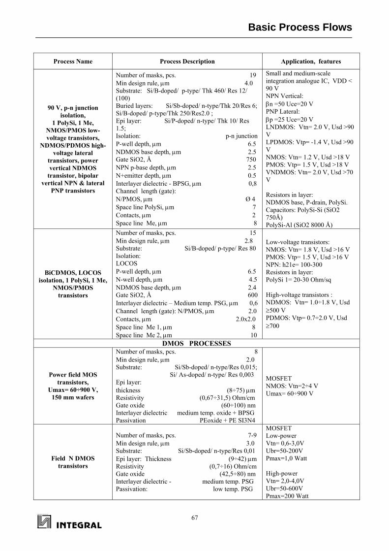
Basic Process Flows
67SEMICONDUCTOR DEVICES
Process Name Process Description Application, features
90 V, p-n junction isolation,
1 PolySi, 1 Me, NMOS/PMOS low-voltage transistors,
NDMOS/PDMOS high-voltage lateral
transistors, power vertical NDMOS
transistor, bipolar vertical NPN & lateral
PNP transistors
Number of masks, pcs. 19 Min design rule, μm 4.0 Substrate: Si/B-doped/ p-type/ Thk 460/ Res 12/ (100) Buried layers: Si/Sb-doped/ n-type/Thk 20/Res 6; Si/B-doped/ p-type/Thk 250/Res2.0 ; Epi layer: Si/P-doped/ n-type/ Thk 10/ Res 1.5; Isolation: p-n junction P-well depth, μm 6.5 NDMOS base depth, μm 2.5 Gate SiO2, Å 750 NPN p-base depth, μm 2.5 N+emitter depth, μm 0.5 Interlayer dielectric - BPSG, μm 0,8 Channel length (gate): N/PMOS, μm Ø 4 Space line PolySi, μm 7 Contacts, μm 2 Space line Me, μm 8
Small and medium-scale integration analogue IC, VDD < 90 V NPN Vertical: βn =50 Uсе=20 V PNP Lateral: βр =25 Uсе=20 V LNDMOS: Vtn= 2.0 V, Usd >90 V LPDMOS: Vtp= -1.4 V, Usd >90 V NMOS: Vtn= 1.2 V, Usd >18 V PMOS: Vtp= 1.5 V, Usd >18 V VNDMOS: Vtn= 2.0 V, Usd >70 V Resistors in layer: NDMOS base, Р-drain, PolySi. Capacitors: PolySi-Si (SiO2 750Å) PolySi-Al (SiO2 8000 Å)
BiCDMOS, LOCOS isolation, 1 PolySi, 1 Me,
NMOS/PMOS transistors
Number of masks, pcs. 15 Min design rule, μm 2.8 Substrate: Si/B-doped/ p-type/ Res 80 Isolation: LOCOS P-well depth, μm 6.5 N-well depth, μm 4.5 NDMOS base depth, μm 2.4 Gate SiO2, Å 600 Interlayer dielectric – Medium temp. PSG, μm 0,6 Channel length (gate): N/PMOS, μm 2.0 Contacts, μm 2.0x2.0 Space line Me 1, μm 8 Space line Me 2, μm 10
Low-voltage transistors: NMOS: Vtn= 1.8 V, Usd >16 V PMOS: Vtp= 1.5 V, Usd >16 V NPN: h21e= 100-300 Resistors in layer: PolySi 1= 20-30 Ohm/sq High-voltage transistors : NDMOS: Vtn= 1.0÷1.8 V, Usd ≥500 V PDMOS: Vtp= 0.7÷2.0 V, Usd ≥700
DMOS PROCESSES
Power field MOS transistors,
Umax= 60÷900 V, 150 mm wafers
Number of masks, pcs. 8 Min design rule, μm 2.0 Substrate: Si/Sb-doped/ n-type/Res 0,015; Si/ As-doped/ n-type/ Res 0,003 Epi layer: thickness (8÷75) μm Resistivity (0,67÷31,5) Ohm/cm Gate oxide (60÷100) nm Interlayer dielectric medium temp. oxide + BPSG Passivation PEoxide + PE SI3N4
MOSFET NMOS: Vtn=2÷4 V Umax= 60÷900 V
Field N DMOS transistors
Number of masks, pcs. 7-9 Min design rule, μm 3.0 Substrate: Si/Sb-doped/ n-type/Res 0,01 Epi layer: Thickness (9÷42) μm Resistivity (0,7÷16) Ohm/cm Gate oxide (42,5÷80) nm Interlayer dielectric - medium temp. PSG Passivation: low temp. PSG
MOSFET Low-power Vtn= 0,6-3,0V Ubr=50-200V Pmax=1,0 Watt High-power Vtn= 2,0-4,0V Ubr=50-600V Pmax=200 Watt
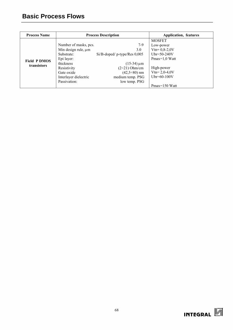
Basic Process Flows
68
Process Name Process Description Application, features
Field P DMOS transistors
Number of masks, pcs. 7-9 Min design rule, μm 3.0 Substrate: Si/B-doped/ p-type/Res 0,005 Epi layer: thickness (15-34) μm Resistivity (2÷21) Ohm/cm Gate oxide (42,5÷80) nm Interlayer dielectric medium temp. PSG Passivation: low temp. PSG
MOSFET Low-power Vtn= 0,8-2,0V Ubr=50-240V Pmax=1,0 Watt High-power Vtn= 2,0-4,0V Ubr=60-100V Pmax=150 Watt
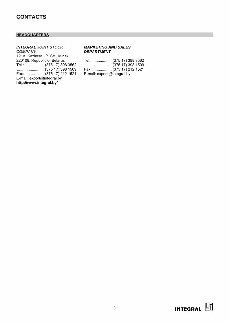
CONTACTS
69
HEADQUARTERS INTEGRAL JOINT STOCK COMPANY 121А, Kazintsa I.P. Str., Minsk, 220108, Republic of Belarus Tel.: ................. (375 17) 398 3562 ......................... (375 17) 398 1509 Fax: ................... (375 17) 212 1521 E-mail: [email protected] http://www.integral.by/
MARKETING AND SALES DEPARTMENT Tel.: ................ (375 17) 398 3562 ......................... (375 17) 398 1509 Fax: .................. (375 17) 212 1521 E-mail: export @integral.by