ON Semiconductor Is Now - onsemi
13
To learn more about onsemi™, please visit our website at www.onsemi.com ON Semiconductor Is Now onsemi and and other names, marks, and brands are registered and/or common law trademarks of Semiconductor Components Industries, LLC dba “onsemi ” or its affiliates and/or subsidiaries in the United States and/or other countries. onsemi owns the rights to a number of patents, trademarks, copyrights, trade secrets, and other intellectual property. A listing of onsemi product/patent coverage may be accessed at www.onsemi.com/site/pdf/Patent-Marking.pdf. onsemi reserves the right to make changes at any time to any products or information herein, without notice. The information herein is provided “as-is” and onsemi makes no warranty, representation or guarantee regarding the accuracy of the information, product features, availability, functionality, or suitability of its products for any particular purpose, nor does onsemi assume any liability arising out of the application or use of any product or circuit, and specifically disclaims any and all liability, including without limitation special, consequential or incidental damages. Buyer is responsible for its products and applications using onsemi products, including compliance with all laws, regulations and safety requirements or standards, regardless of any support or applications information provided by onsemi. “Typical” parameters which may be provided in onsemi data sheets and/ or specifications can and do vary in different applications and actual performance may vary over time. All operating parameters, including “Typicals” must be validated for each customer application by customer’s technical experts. onsemi does not convey any license under any of its intellectual property rights nor the rights of others. onsemi products are not designed, intended, or authorized for use as a critical component in life support systems or any FDA Class 3 medical devices or medical devices with a same or similar classification in a foreign jurisdiction or any devices intended for implantation in the human body. Should Buyer purchase or use onsemi products for any such unintended or unauthorized application, Buyer shall indemnify and hold onsemi and its officers, employees, subsidiaries, affiliates, and distributors harmless against all claims, costs, damages, and expenses, and reasonable attorney fees arising out of, directly or indirectly, any claim of personal injury or death associated with such unintended or unauthorized use, even if such claim alleges that onsemi was negligent regarding the design or manufacture of the part. onsemi is an Equal Opportunity/Affirmative Action Employer. This literature is subject to all applicable copyright laws and is not for resale in any manner. Other names and brands may be claimed as the property of others.
-
Upload
khangminh22 -
Category
Documents
-
view
0 -
download
0
Transcript of ON Semiconductor Is Now - onsemi

To learn more about onsemi™, please visit our website at www.onsemi.com
ON Semiconductor
Is Now
onsemi and and other names, marks, and brands are registered and/or common law trademarks of Semiconductor Components Industries, LLC dba “onsemi” or its affiliates and/or subsidiaries in the United States and/or other countries. onsemi owns the rights to a number of patents, trademarks, copyrights, trade secrets, and other intellectual property. A listing of onsemi product/patent coverage may be accessed at www.onsemi.com/site/pdf/Patent-Marking.pdf. onsemi reserves the right to make changes at any time to any products or information herein, without notice. The information herein is provided “as-is” and onsemi makes no warranty, representation or guarantee regarding the accuracy of the information, product features, availability, functionality, or suitability of its products for any particular purpose, nor does onsemi assume any liability arising out of the application or use of any product or circuit, and specifically disclaims any and all liability, including without limitation special, consequential or incidental damages. Buyer is responsible for its products and applications using onsemi products, including compliance with all laws, regulations and safety requirements or standards, regardless of any support or applications information provided by onsemi. “Typical” parameters which may be provided in onsemi data sheets and/or specifications can and do vary in different applications and actual performance may vary over time. All operating parameters, including “Typicals” must be validated for each customer application by customer’s technical experts. onsemi does not convey any license under any of its intellectual property rights nor the rights of others. onsemi products are not designed, intended, or authorized for use as a critical component in life support systems or any FDA Class 3 medical devices or medical devices with a same or similar classification in a foreign jurisdiction or any devices intended for implantation in the human body. Should Buyer purchase or use onsemi products for any such unintended or unauthorized application, Buyer shall indemnify and hold onsemi and its officers, employees, subsidiaries, affiliates, and distributors harmless against all claims, costs, damages, and expenses, and reasonable attorney fees arising out of, directly or indirectly, any claim of personal injury or death associated with such unintended or unauthorized use, even if such claim alleges that onsemi was negligent regarding the design or manufacture of the part. onsemi is an Equal Opportunity/Affirmative Action Employer. This literature is subject to all applicable copyright laws and is not for resale in any manner. Other names and brands may be claimed as the property of others.

© Semiconductor Components Industries, LLC, 2009
October, 2009 − Rev. 21 Publication Order Number:
AND8324/D
AND8324/D
300 W, Wide Mains, PFCStage Driven by theNCP1654
Prepared by: Patrick WangON Semiconductor
IntroductionThe NCP1654 is a Power Factor Controller to efficiently
drive Continuous Conduction Mode (CCM) step−uppre−converters. As shown by the ON Semiconductorapplication note AND8322, “Four Key Steps to Design aContinuous Conduction Mode PFC Stage Using theNCP1654”, which details the four key steps to design aNCP1654 driven PFC stage, this circuit represents a majorleap towards compactness and ease of implementation.
Housed in a SO−8 package, the circuit minimizes theexternal components count without sacrificing performanceand flexibility. In particular, the NCP1654 integrates all thekey protections to build robust PFC stages like an effectiveinput power runaway clamping circuitry.
When needed or wished, the NCP1654 also allowsoperation in Follower Boost mode(1) to drastically lower thepre−converter size and cost, in a straight−forward manner.For more information on this device, please refer to theON Semiconductor data sheet NCP1654/D.
The board illustrates the circuit capability to effectivelydrive a high power, universal line application. Morespecifically, it is designed to meet the followingspecifications:• Maximum output power: 300 W
• Input voltage range: from 85 VRMS to 265 VRMS
• Regulation output voltage: 390 V
• Switching frequency: 65 kHz
This application was tested using an active load. As inmany applications, the PFC controller is fed by an output ofthe downstream converter, there is generally no need for anauto−supply circuitry. Hence, in our demo board, theNCP1654 VCC is to be supplied by a 15 V external powersupply.
The external voltage source that is to be applied to theNCP1654 VCC, should exceed 10.5 V typical, to allow thecircuits start up. After start up, the VCC operating range isfrom 9 V to 20 V.
The voltage applied to the NCP1654 VCC must NOTexceed 20 V.
The NCP1654 is a continuous conduction mode and fixedfrequency controller (65 kHz). The coil (650 uH) is selectedto limit the peak to peak current ripple in the range of 36 %at the sinusoid top, in full load and low line conditions.Again, for details on how the application is designed, pleaserefer to the ON Semiconductor application note AND8322,”Four Key Steps to Design a Continuous Conduction ModePFC Stage Using the NCP1654”.
As detailed in the document, the board yields very nicePower Factor ratios and effectively limits the TotalHarmonic Distortion (THD).
http://onsemi.com

AND8324/D
http://onsemi.com2
Figure 1. Application Schematic
TB
2
1 2
390V
+
+
1 2
TB
3
+15
V
C4
R1
1.8M
R2
1.8M
MS
R86
0G
D1
D2
1N41
48
R5 10
R4
10k
Q1
SP
P20
N60
S5
180�
F 4
50V
C8
22�F
C9
0.1�
F
C10
10pF
R3
23.2
k
C12
2.2�
F
C5
220n
F
R12
12k
L1
52
650�
H
8 7 6 54321
GN
D
VM
CS
BO
DR
V
VC
C FB
Vco
ntro
l
R6
0.1
R7
3.6k
R8
47k
R9
3.3M
R13
3.3M
R10
0 R11
82.5
kC
6
1nF
C7
0.47
�F
C3
0.1�
F
GB
U8J
8A
600
VD
B1
C2
0.47
�F
L2
2 x
6.8m
H
C1
0.47
�F
150�
HL3
TB
1
AC
Inle
t
L H
1 2 3
5A F
use
F1
IC1
NC
P16
54

AND8324/D
http://onsemi.com3
Table 1. BILL OF MATERIAL
Reference Description Part Number Manufacturer
C1 0.47 uF / 275 V type X2 F1772−447−2000 VISHAY
C2 0.47 uF / 275 V type X2 F1772−447−2000 VISHAY
C3 0.1u, 400V, High Ripple, Polypropylene Cap ECWF4104JL Matsushita
C4 180 �F 450 V 2222 159 47181 BC Components
C5 0.22 �F / 50V K224K20X7RF53H5 VISHAY
C7 0.47 �F / 50V K474K20X7RF53H5 VISHAY
C9 0.1 �F / 50V K104K15X7RF53H5 VISHAY
C6 1 nF / 50 V K102K15X7RF53H5 VISHAY
C10 100 pF / 50 V K101K15X7RF53H5 VISHAY
C8 22 �F / 25 V 2222 013 36229 BC Components
C12 2.2 �F / 50 V B32529D5225J EPCOS
DB1 600 V, 8.0 A Bridge Dode GBU8J VISHAY
D1 8.0 A, 600 V MSR860G ON Semiconductor
D2 1N4148 1N4148 VISHAY
F1 5 A Fuse, Time Delay Fuse (FST 5x20) 0034.3124 SCHURTER
IC1 CCM PFC Controller NCP1654 ON Semiconductor
L1 650 �H GA3199−AL CoilCraft
2702.0010A Pulse
L2 4 A, 2 x 6.8 mH, CM Choke B82725−J2402−N20 EPCOS
L3 150 uH, 5A, WE−FI Series, DM Choke 7447055 Wurth Elektronik
Q1 20 A 600 V MOSFET SPP20N60C3 Infineon
R1 Resistor, Axial Lead, 1.8 M, 1/4 W, 1% CCF501M80FKE36 VISHAY
R2 Resistor, Axial Lead, 1.8 M, 1/4 W, 1% CCF501M80FKE36 VISHAY
R9 Resistor, Axial Lead, 3.3 M, 1/4 W, 1% CCF503M30FKE36 VISHAY
R13 Resistor, Axial Lead, 3.3 M, 1/4 W, 1% CCF503M30FKE36 VISHAY
R10 Jumper Jumper
R3 Resistor, Axial Lead, 23.2 k, 1/4 W, 1% CCF5023K2FKE36 VISHAY
R4 Resistor, Axial Lead, 10 k, 1/4 W CCF5010K0FKE36 VISHAY
R5 Resistor, Axial Lead, 10, 1/4 W CCF5010R0FKE36 VISHAY
R6 Resistor, Axial Lead, 0.1, 3 W, 1% LVR3 Series LVR03 R1000 F E12 VISHAY
R7 Resistor, Axial Lead, 3.6 k, 1/4 W 1% CCF503K60FKE36 VISHAY
R8 Resistor, Axial Lead, 47 k, 1/4 W CCF5047K0FKE36 VISHAY
R11 Resistor, Axial Lead, 82.5 k, 1/4 W, 1% CCF5082K5FKE36 VISHAY
R12 Resistor, Axial Lead, 12 k, 1/4 W, 1% CCF5012K0FKE36 VISHAY
TB1 AC Inlet Connector GSF1.1201.31 SCHURTER
TB2 DC Output Plug Socket 20.101/2(Order Code 3044531)
IMO
TB3 VCC Connector Plug Socket PM5.08/2/90.(Order Code 5015571)
WEIDMULLER
HS1 Heatsink(2.9°C/W) SK481 100mm Fischer Elektronik
Q1 Isolator TO−220 3223−07FR−43 BERGQUIST
D1 Isolator TO−220 3223−07FR−43 BERGQUIST
DB1 Clip for heatsink (TO−220) THFU 1 Fischer Elektronik
Q1 Clip for heatsink (TO−220) THFU 1 Fischer Elektronik
D1 Clip for heatsink (TO−220) THFU 1 Fischer Elektronik
PCB
Board Legs TCBS−801 RICHCO
Board Legs TCBS−801 RICHCO
Board Legs TCBS−801 RICHCO
Board Legs TCBS−801 RICHCO

AND8324/D
http://onsemi.com4
Figure 2. The Board
Two coils from two different vendors have been validatedon this board:• GA3199−AL from Coil Craft
• 2702.0010A from Pulse
For the sake of consistency, this application note reportsthe performance and results that were obtained using theCoilCraft. However, it has been checked that the other coilyield high performance too.
AND8324/D
http://onsemi.com5
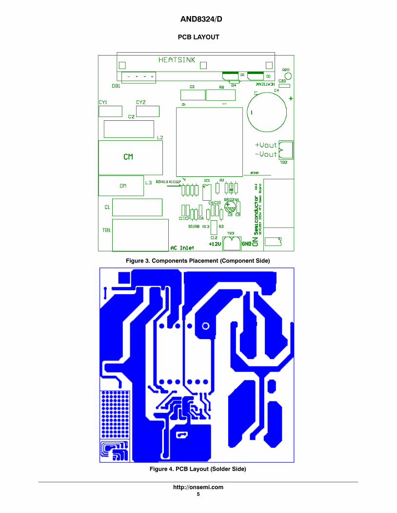
PCB LAYOUT
Figure 3. Components Placement (Component Side)
Figure 4. PCB Layout (Solder Side)
AND8324/D
http://onsemi.com6
GENERAL BEHAVIOR
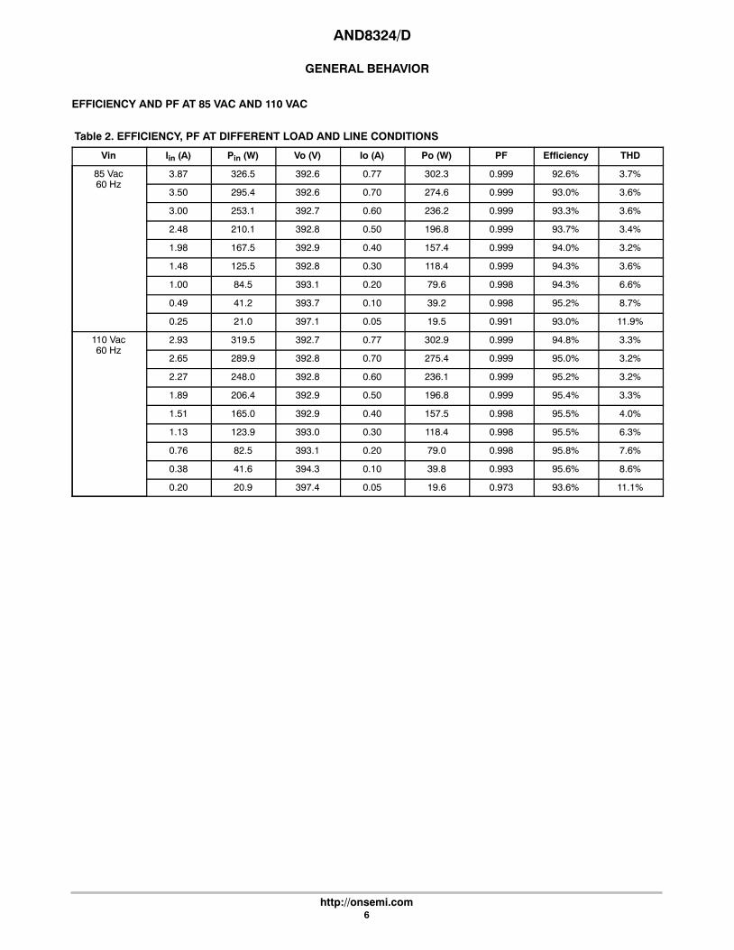
EFFICIENCY AND PF AT 85 VAC AND 110 VAC
Table 2. EFFICIENCY, PF AT DIFFERENT LOAD AND LINE CONDITIONS
Vin Iin (A) Pin (W) Vo (V) Io (A) Po (W) PF Efficiency THD
85 Vac60 Hz
3.87 326.5 392.6 0.77 302.3 0.999 92.6% 3.7%
3.50 295.4 392.6 0.70 274.6 0.999 93.0% 3.6%
3.00 253.1 392.7 0.60 236.2 0.999 93.3% 3.6%
2.48 210.1 392.8 0.50 196.8 0.999 93.7% 3.4%
1.98 167.5 392.9 0.40 157.4 0.999 94.0% 3.2%
1.48 125.5 392.8 0.30 118.4 0.999 94.3% 3.6%
1.00 84.5 393.1 0.20 79.6 0.998 94.3% 6.6%
0.49 41.2 393.7 0.10 39.2 0.998 95.2% 8.7%
0.25 21.0 397.1 0.05 19.5 0.991 93.0% 11.9%
110 Vac60 Hz
2.93 319.5 392.7 0.77 302.9 0.999 94.8% 3.3%
2.65 289.9 392.8 0.70 275.4 0.999 95.0% 3.2%
2.27 248.0 392.8 0.60 236.1 0.999 95.2% 3.2%
1.89 206.4 392.9 0.50 196.8 0.999 95.4% 3.3%
1.51 165.0 392.9 0.40 157.5 0.998 95.5% 4.0%
1.13 123.9 393.0 0.30 118.4 0.998 95.5% 6.3%
0.76 82.5 393.1 0.20 79.0 0.998 95.8% 7.6%
0.38 41.6 394.3 0.10 39.8 0.993 95.6% 8.6%
0.20 20.9 397.4 0.05 19.6 0.973 93.6% 11.1%

AND8324/D
http://onsemi.com7
Table 3. EFFICIENCY AND PF AT 230 VAC AND 265 VAC
Vin Iin (A) Pin (W) Vo (V) Io (A) Po (W) PF Efficiency THD
230 Vac50 Hz
1.36 309.4 393 0.77 303.0 0.996 97.9% 6.1%
1.23 281.0 393 0.70 275.1 0.995 97.9% 6.3%
1.05 240.7 393.1 0.60 235.5 0.994 97.9% 7.1%
0.89 201.5 393.2 0.50 197.1 0.992 97.8% 7.1%
0.71 161.3 393.2 0.40 157.7 0.990 97.8% 7.2%
0.54 121.1 393.3 0.30 118.2 0.983 97.6% 7.4%
0.37 81 393.7 0.20 78.8 0.966 97.3% 7.3%
0.20 41.1 394.6 0.10 39.6 0.892 96.5% 13.0%
0.12 20.6 395.4 0.05 19.4 0.752 94.5% 15.8%
265 Vac50 Hz
1.18 308.2 393 0.77 302.3 0.993 98.1% 6.9%
1.07 281.1 393.1 0.70 275.8 0.992 98.1% 6.8%
0.92 241.2 393.1 0.60 236.5 0.991 98.0% 6.7%
0.77 201.2 393.2 0.50 197.1 0.988 98.0% 7.0%
0.62 161.2 393.2 0.40 157.8 0.982 97.9% 6.9%
0.47 121.1 393.4 0.30 118.4 0.972 97.8% 7.3%
0.33 81.4 393.8 0.20 79.0 0.943 97.1% 11.8%
0.19 41.1 394.5 0.10 39.7 0.840 96.6% 22.6%
0.13 21.5 395 0.05 20.4 0.650 94.7% 23.0%
Figure 5. Efficiency vs. Input Voltage
92
93
94
95
96
97
98
99
85 170 255
EF
FIC
IEN
CY
(%
)
INPUT VOLTAGE (Vac)
FULL LOAD
HALF LOAD
340
Figure 6. Power Factor vs. Output Power
0.90
0.91
0.92
0.93
0.94
0.95
0.96
0.97
0.98
0.99
1.0
70 170 270
OUTPUT POWER
PO
WE
R F
AC
TO
R
85Vac
110Vac
230Vac
265Vac
AND8324/D
http://onsemi.com8
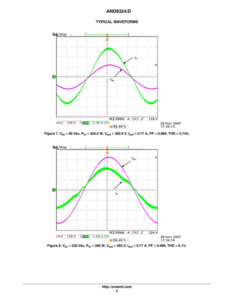
TYPICAL WAVEFORMS
Figure 7. Vac = 85 Vac, Pin = 326.5 W, Vout = 392.6 V, Iout = 0.77 A, PF = 0.999, THD = 3.74%
Iin
Vac
Figure 8. Vac = 230 Vac, Pin = 309 W, Vout = 393 V, Iout = 0.77 A, PF = 0.996, THD = 6.1%
Iin
Vac

AND8324/D
http://onsemi.com9
NO LOAD OPERATION
Figure 9. Vac = 230 Vac, Pin = 147 mW, Vout = 396 V, Iout = 0 A
Iin
Vin
Vout
VM
When in light load, the circuit enters a welcome burstmode that enables the circuit to keep regulating. VM pinoscillates around its internal reference voltage (2.5 V).
The power losses @ 230 Vac are nearly 147 mW. Thisresult was obtained by using a W.h. meter (measureduration: 1 sec)
Soft−StartThe NCP1654 grounds the “Vcontrol” capacitor when it is
off, i.e., before each circuit active sequence (“Vcontrol” beingthe regulation block output). Only charging by the 28−�Ainternal current source of the error amplifier (the 200 �A ofthe dynamic response enhancer being disabled during thestart−up phase), “Vcontrol” ramps up slowly. As a result, thepower delivery rises gradually and the PFC pre−regulatorstarts up smoothly and noiselessly.
Figure 10. Vac = 85 Vac, Vout = 392.6 V, Iout = 0.77 A
Iin
DRV
Vout
Vcontrol

AND8324/D
http://onsemi.com10
Transient LoadWhen output loading changes from full load to no load,
the output voltage raises, and Vfb rises to activate the OVPfunction. The output voltage is clamped by the OVPfunction.
When output loading changes from no load to full load,the output voltage drops, Vfb drops below 95% of Vref,
Vcontrol is sharply pulled high by the internal 200 �A currentsource of the dynamic response enhancer. As a result, ahigher power is delivered to output. Hence it prevents theoutput voltage from dropping deeply.
Figure 11. Vac = 85 Vac, Vout = 392.6 V, Iout = 0 A ~ 0.77 A
Iin
Vout
Vcontrol

AND8324/D
http://onsemi.com11
Under Voltage Protection (UVP)FB open test at 265 Vac, Iout = 0.1 A. The PFC circuit operates first, then short the FB Pin to ground. As Vfb is lower than
8% of Vref, UVP activates and shuts down the output. It is to protect the buck capacitor from damaging.
Figure 12. Vac = 265 Vac, Vout = 394.5 V, Iout = 0.1 A
Iin
Vout
Vfb
DRV
Brown Out TestWhen the input voltage decreases to 68 Vac, VBO is below 0.7 V, brown out function is triggered and driver stops.
Figure 13. Vac = 68 Vac, Vout = 393.7 V, Iout = 0.1 A
Iin
Vout
Vac
VBO

AND8324/D
http://onsemi.com12
Brown Out Recovery TestWhen the input voltage increases above 78.4 Vac, VBO is above 1.3 V and driver resumes operation.
Figure 14. Vac = 78.4 Vac, Vout = 393.7 V, Iout = 0.1 A
Iin
Vout
Vac
VBO
ON Semiconductor and are registered trademarks of Semiconductor Components Industries, LLC (SCILLC). SCILLC reserves the right to make changes without further noticeto any products herein. SCILLC makes no warranty, representation or guarantee regarding the suitability of its products for any particular purpose, nor does SCILLC assume any liabilityarising out of the application or use of any product or circuit, and specifically disclaims any and all liability, including without limitation special, consequential or incidental damages.“Typical” parameters which may be provided in SCILLC data sheets and/or specifications can and do vary in different applications and actual performance may vary over time. Alloperating parameters, including “Typicals” must be validated for each customer application by customer’s technical experts. SCILLC does not convey any license under its patent rightsnor the rights of others. SCILLC products are not designed, intended, or authorized for use as components in systems intended for surgical implant into the body, or other applicationsintended to support or sustain life, or for any other application in which the failure of the SCILLC product could create a situation where personal injury or death may occur. ShouldBuyer purchase or use SCILLC products for any such unintended or unauthorized application, Buyer shall indemnify and hold SCILLC and its officers, employees, subsidiaries, affiliates,and distributors harmless against all claims, costs, damages, and expenses, and reasonable attorney fees arising out of, directly or indirectly, any claim of personal injury or deathassociated with such unintended or unauthorized use, even if such claim alleges that SCILLC was negligent regarding the design or manufacture of the part. SCILLC is an EqualOpportunity/Affirmative Action Employer. This literature is subject to all applicable copyright laws and is not for resale in any manner.
PUBLICATION ORDERING INFORMATIONN. American Technical Support: 800−282−9855 Toll FreeUSA/Canada
Europe, Middle East and Africa Technical Support:Phone: 421 33 790 2910
Japan Customer Focus CenterPhone: 81−3−5773−3850
AND8324/D
LITERATURE FULFILLMENT:Literature Distribution Center for ON SemiconductorP.O. Box 5163, Denver, Colorado 80217 USAPhone: 303−675−2175 or 800−344−3860 Toll Free USA/CanadaFax: 303−675−2176 or 800−344−3867 Toll Free USA/CanadaEmail: [email protected]
ON Semiconductor Website: www.onsemi.com
Order Literature: http://www.onsemi.com/orderlit
For additional information, please contact your localSales Representative