NCP1607 - Cost Effective Power Factor Controller - onsemi
25
© Semiconductor Components Industries, LLC, 2015 July, 2015 - Rev. 2 1 Publication Order Number: NCP1607/D NCP1607 Cost Effective Power Factor Controller The NCP1607 is an active power factor controller specifically designed for use as a pre-converter in ac-dc adapters, electronic ballasts, and other medium power off line converters (typically up to 250 W). It utilizes Critical Conduction Mode (CRM) to ensure unity power factor across a wide range of input voltages and power levels. The NCP1607 minimizes the number of external components. The integration of comprehensive safety protection features makes it an excellent choice for designing robust PFC stages. It is available in a SOIC-8 package. General Features • “Unity” Power Factor • No Need for Input Voltage Sensing • Latching PWM for Cycle by Cycle On Time Control (Voltage Mode) • High Precision Voltage Reference (±1.6% over the Temperature Range) • Very Low Startup Current Consumption (≤ 40 mA) • Low Typical Operating Current (2.1 mA) • Source 500 mA / Sink 800 mA Totem Pole Gate Driver • Undervoltage Lockout with Hysteresis • Pin to Pin Compatible with Industry Standards • This is a Pb-Free Device • This Device uses Halogen-Free Molding Compound Safety Features • Programmable Overvoltage Protection • Open Feedback Loop Protection • Accurate and Programmable On Time Control • Accurate Overcurrent Detector Typical Applications • AC-DC Adapters, TVs, Monitors • Off Line Appliances Requiring Power Factor Correction • Electronic Light Ballast Figure 1. Typical Application + AC Line EMI Filter 1 4 3 2 8 5 6 7 + C BULK LOAD (Ballast, SMPS, etc.) NCP1607 V OUT R S C IN R ZCD R OUT1 R OUT2 C COMP V CC C T D BOOST L BOOST FB Control Ct CS GND ZCD DRV V CC www. onsemi.com SO-8 D SUFFIX CASE 751 MARKING DIAGRAMS PIN CONNECTION 1 8 A = Assembly Location L = Wafer Lot Y = Year W = Work Week G = Pb-Free Package 1607B ALYW G 1 8 FB Control Ct CS V CC DRV GND ZCD (Top View) Device Package Shipping † ORDERING INFORMATION †For information on tape and reel specifications, including part orientation and tape sizes, please refer to our Tape and Reel Packaging Specifications Brochure, BRD8011/D. NCP1607BDR2G SOIC-8 (Pb-Free) 2500 / Tape & Reel
-
Upload
khangminh22 -
Category
Documents
-
view
0 -
download
0
Transcript of NCP1607 - Cost Effective Power Factor Controller - onsemi

© Semiconductor Components Industries, LLC, 2015
July, 2015 − Rev. 21 Publication Order Number:
NCP1607/D
NCP1607
Cost Effective Power Factor
Controller
The NCP1607 is an active power factor controller specificallydesigned for use as a pre−converter in ac−dc adapters, electronicballasts, and other medium power off line converters (typically up to250 W). It utilizes Critical Conduction Mode (CRM) to ensure unitypower factor across a wide range of input voltages and power levels.The NCP1607 minimizes the number of external components. Theintegration of comprehensive safety protection features makes it anexcellent choice for designing robust PFC stages. It is available in aSOIC−8 package.
General Features
• “Unity” Power Factor• No Need for Input Voltage Sensing
• Latching PWM for Cycle by Cycle On Time Control (Voltage Mode)
• High Precision Voltage Reference (±1.6% over the TemperatureRange)
• Very Low Startup Current Consumption (≤ 40 �A)• Low Typical Operating Current (2.1 mA)
• Source 500 mA / Sink 800 mA Totem Pole Gate Driver
• Undervoltage Lockout with Hysteresis
• Pin to Pin Compatible with Industry Standards• This is a Pb−Free Device
• This Device uses Halogen−Free Molding Compound
Safety Features• Programmable Overvoltage Protection• Open Feedback Loop Protection
• Accurate and Programmable On Time Control
• Accurate Overcurrent Detector
Typical Applications
• AC−DC Adapters, TVs, Monitors• Off Line Appliances Requiring Power Factor Correction
• Electronic Light Ballast
Figure 1. Typical Application
+
AC LineEMI Filter
1
4
3
2
8
5
6
7
+CBULK
LOAD (Ballast,
SMPS, etc.)NCP1607
VOUT
RS
CIN
RZCD
ROUT1
ROUT2
CCOMP
VCC
CT
DBOOST
LBOOST
FB
Control
Ct
CS
GND
ZCD
DRV
VCC
www.onsemi.com
SO−8D SUFFIXCASE 751
MARKINGDIAGRAMS
PIN CONNECTION
1
8
A = Assembly LocationL = Wafer LotY = YearW = Work Week� = Pb−Free Package
1607BALYW
�1
8
FBControl
CtCS
VCCDRVGNDZCD
(Top View)
Device Package Shipping†
ORDERING INFORMATION
†For information on tape and reel specifications,including part orientation and tape sizes, pleaserefer to our Tape and Reel Packaging SpecificationsBrochure, BRD8011/D.
NCP1607BDR2G SOIC−8(Pb−Free)
2500 / Tape & Reel

NCP1607
www.onsemi.com2
Figure 2. Block Diagram
UVLO
DRV
GND
FB
Control
CS
ZCD
E/A
+−
Measure
+
+
+
+
+
VCL(POS)Clamp
Shutdown
Demag
UVP
Fault
OCP
+−+
Dynamic OVP
Shutdown
VEAHClamp
Active Clamp
LEB
Add VEALOffset
Static OVP is triggeredwhen clamp is activated.
VEALClamp
Static OVP
Off Timer
Reset
PWM
R
QS
(Enable EA)
+
R
QS
R
QS
R
QS
R
QS
AC IN
DRV
VCONTROL
ROUT2
ROUT1
CCOMP
RS
RZCD
CBULK
Q
Q
Q
VCC
VOUT
VCC
Q
Q
VDD
VDD
ICHARGE
VDD
VCC
VDD
VDDGD
VDD Reg
IEAsink
Isink>Iovp
VCL(NEG)
*All SR Latches are Reset Dominant
+−
+−
+−
+−
+−
Enable
+−
VCS(limit)
DBOOST
LBOOST
uVDD
uVDD
uVDD
VDDGD
UVLO
RFB
VREF
VUVP
POK
POK
VZCDH
VZCDL
VSDL
POK
CT
CT
ESD
ESD
ESD
ESD

NCP1607
www.onsemi.com3
PIN FUNCTION DESCRIPTION
Pin Name Function
1 FB The FB pin is the inverting input of the internal error amplifier. An external resistor divider scales the output voltage to theinternal reference voltage to maintain regulation. The feedback information is also used for the programmable overvoltageand undervoltage protections. The controller is disabled when this pin is below the undervoltage protection threshold,VUVP, typically 0.3 V.
2 Control The Control pin is the output of the internal error amplifier. A compensation network is placed between the Control and FBpins to set the loop bandwidth. A low enough bandwidth is needed to obtain a high power factor ratio and a low THD.
3 Ct The Ct pin sources a current to charge an external timing capacitor. The circuit controls the power switch on time by com-paring the Ct voltage to an internal voltage derived from the regulation block. The Ct pin discharges the external timingcapacitor at the end of the switching cycle.
4 CS The CS pin limits the cycle−by−cycle current through the power switch. When the CS voltage exceeds the internal thresh-old, the MOSFET driver turns off. The sense resistor that connects to the CS pin programs the maximum switch current.
5 ZCD The voltage of an auxiliary winding is applied to this pin to detect when the inductor is demagnetized for critical conductionmode operation. The controller is disabled when this pin is grounded.
6 GND Analog ground.
7 DRV Integrated MOSFET driver capable of driving a high gate charge power MOSFET.
8 VCC The VCC pin is the positive supply of the controller. The controller is enabled when VCC exceeds VCC(on) and remainsenabled until VCC decreases below VCC(off).
MAXIMUM RATINGS
Rating Symbol Value Unit
Supply Voltage VCC −0.3 to 20 V
Supply Current ICC ±20 mA
DRV Voltage VDRV −0.3 to 20 V
DRV Sink Current IDRV(sink) 800 mA
DRV Source Current IDRV(source) 500 mA
FB Voltage VFB −0.3 to 10 V
FB Current IFB ±10 mA
Control Voltage VCONTROL −0.3 to 10 V
Control Current ICONTROL −2 to 10 mA
Ct Voltage VCt −0.3 to 6 V
Ct Current ICt ±10 mA
CS Voltage VCS −0.3 to 6 V
CS Current ICS ±10 mA
ZCD Voltage VZCD −0.3 to 10 V
ZCD Current IZCD ±10 mA
Power Dissipation and Thermal CharacteristicsD suffix, Plastic Package, Case 751Maximum Power Dissipation @ TA = 70°CThermal Resistance Junction−to−Air
PD(SO)R�JA(SO)
450178
mW°C/W
Operating Junction Temperature Range TJ −40 to 125 °C
Maximum Junction Temperature TJ(MAX) 150 °C
Storage Temperature Range TSTG −65 to 150 °C
Lead Temperature (Soldering, 10 s) TL 300 °C
Stresses exceeding those listed in the Maximum Ratings table may damage the device. If any of these limits are exceeded, device functionalityshould not be assumed, damage may occur and reliability may be affected.1. This device series contains ESD protection and exceeds the following tests:
Pins 1 − 8: Human Body Model 2000 V per JEDEC Standard JESD22−A114E,Charged Device Model 1000 V per JEDEC Standard JESD22−C101E.
2. This device contains latch−up protection and exceeds ±100 mA per JEDEC Standard JESD78.

NCP1607
www.onsemi.com4
ELECTRICAL CHARACTERISTICS(For typical values, TJ = 25°C. For min/max values, TJ = −40°C to +125°C, unless otherwise specified, VCC = 12 V, VFB = 2.4 V, VCS = 0 V, VCONTROL = open, VZCD = open, CDRV = 1 nF, CT = 1 nF)
Characteristics Symbol Min Typ Max Unit
VCC UNDERVOLTAGE LOCKOUT SECTION
VCC Startup Threshold (Undervoltage Lockout Threshold, Vcc rising)−25°C < TJ < +125°C−40°C < TJ < +125°C
VCC(on)11.010.9
11.811.8
13.013.1
V
VCC Disable Voltage after Turn On (Undervoltage Lockout Threshold, VCC falling)−25°C < TJ < +125°C−40°C < TJ < +125°C
VCC(off)8.78.5
9.59.5
10.310.5
V
Undervoltage Lockout Hysteresis HUVLO 2.2 2.5 2.8 V
DEVICE CONSUMPTION
ICC consumption during startup: 0 V < VCC < VCC(on) − 200 mV ICC(startup) − 23.5 40 �A
ICC consumption after turn on at No Load, 70 kHz switching ICC1 − 1.4 2.0 mA
ICC consumption after turn on at 70 kHz switching ICC2 − 2.17 3.0 mA
ICC consumption after turn on at no switching(such as during OVP fault, UVP fault, or grounding ZCD)
ICC(fault) − 1.2 1.6 mA
REGULATION BLOCK (ERROR AMPLIFIER)
Voltage Reference TJ = 25 °C−25°C < TJ < +125°C−40°C < TJ < +125°C
VREF 2.4752.4652.460
2.502.502.50
2.5252.5352.540
V
VREF Line Regulation from VCC(on) + 200 mV < VCC < 20 V, TJ = 25°C VREF(line) −2.0 − 2.0 mV
Error Amplifier Current Capability: (Note 3)Sink (VControl = 4 V, VFB = 2.6 V):Source (VControl = 4 V, VFB = 2.4 V):
IEA8.0−2.0
17−6.0
−−
mA
Error Amplifier Open Loop DC Gain (Note 4) GOL − 80 − dB
Unity Gain Bandwidth (Note 4) BW − 1.0 − MHz
FB Bias Current (VFB = 2.5 V) IFB 0.25 0.53 1.25 �A
FB Pull Down Resistor (VFB = 2.5 V) RFB 2.0 4.7 10 M�
Control Pin Bias Current (FB = 0 V and VCONTROL = 4.0 V) ICONTROL −1.0 − 1.0 �A
VCONTROL (IEASOURCE = 0.5 mA, VFB = 2.4 V) VEAH 4.9 5.3 5.7 V
VCONTROL (IEASINK = 0.5 mA, VFB = 2.6 V) VEAL 1.85 2.1 2.4 V
VEA(diff) = VEAH − VEAL VEA(diff) 3.0 3.2 3.4 V
CURRENT SENSE BLOCK
Overcurrent Voltage Threshold VCS(limit) 0.45 0.5 0.55 V
Leading Edge Blanking Duration tLEB 150 256 350 ns
Overcurrent Voltage Propagation Delay tCS 40 100 170 ns
CS Bias Current (VCS = 2 V) ICS −1.0 − 1.0 �A
ZERO CURRENT DETECTION
Zero Current Detection Threshold (VZCD rising) VZCDH 1.9 2.1 2.3 V
Zero Current Detection Threshold (VZCD falling) VZCDL 1.45 1.6 1.75 V
VZCDH − VZCDL VZCD(HYS) 300 500 800 mV
Maximum ZCD bias Current (VZCD = 5 V) IZCD −2.0 − +2.0 �A
Upper Clamp Voltage (IZCD = 2.5 mA) VCL(POS) 5.0 5.7 6.5 V
Current Capability of the Positive Clamp at VZCD = VCL(POS) + 200 mV: ICL(POS) 5.0 8.5 − mA
Negative Active Clamp Voltage (IZCD = −2.5 mA) VCL(NEG) 0.45 0.6 0.75 V
3. Parameter values are valid for transient conditions only.4. Parameter characterized and guaranteed by design, but not tested in production.

NCP1607
www.onsemi.com5
ELECTRICAL CHARACTERISTICS(For typical values, TJ = 25°C. For min/max values, TJ = −40°C to +125°C, unless otherwise specified, VCC = 12 V, VFB = 2.4 V, VCS = 0 V, VCONTROL = open, VZCD = open, CDRV = 1 nF, CT = 1 nF)
Characteristics UnitMaxTypMinSymbol
Current Capability of the Negative Active Clamp:in normal mode (VZCD = 300 mV)in shutdown mode (VZCD = 100 mV)
ICL(NEG)
2.535
3.770
5.0100
mA�A
Shutdown Threshold (VZCD falling) VSDL 150 205 250 mV
Enable Threshold (VZCD rising) VSDH − 290 350 mV
Shutdown Comparator Hysteresis VSD(HYS) − 85 − mV
Zero Current Detection Propagation Delay tZCD − 100 170 ns
Minimum Detectable ZCD Pulse Width tSYNC − 70 − ns
Drive off Restart Timer tSTART 75 179 300 �s
RAMP CONTROL
Ct Charge Current (VCT = 0 V) −25°C < TJ < +125°C−40°C < TJ < +125°C
ICHARGE 243235
270270
297297
�A
Time to discharge a 1 nF Ct capacitor from VCT = 3.4 V to 100 mV. tCT(discharge) − − 100 ns
Maximum Ct level before DRV switches off −25°C < TJ < +125°C−40°C < TJ < +125°C
VCTMAX 2.92.9
3.23.2
3.33.4
V
PWM Propagation Delay tPWM − 142 220 ns
OVER AND UNDERVOLTAGE PROTECTION
Dynamic Overvoltage Protection (OVP) Triggering Current:TJ = 25°CTJ = −40°C to +125°C
IOVP9.08.7
10.5−
11.812.1
�A
Hysteresis of the dynamic OVP current before the OVP latch is released IOVP(HYS) − 8.5 − �A
Static OVP Threshold Voltage VOVP − VEAL +100 mV
− V
Undervoltage Protection (UVP) Threshold Voltage VUVP 0.25 0.302 0.4 V
GATE DRIVE SECTION
Gate Drive Resistance:ROH @ ISOURCE = 100 mAROL @ ISINK = 100 mA
ROHROL
−−
126.0
1810
�
Drive voltage rise time from 10% VCC to 90% VCC trise − 30 80 ns
Drive voltage fall time from 90% VCC to 10% VCC tfall − 25 70 ns
Driver output voltage at VCC = VCC(on) − 200 mV and Isink = 10 mA VOUT(start) − − 0.2 V
3. Parameter values are valid for transient conditions only.4. Parameter characterized and guaranteed by design, but not tested in production.
Product parametric performance is indicated in the Electrical Characteristics for the listed test conditions, unless otherwise noted. Productperformance may not be indicated by the Electrical Characteristics if operated under different conditions.

NCP1607
www.onsemi.com6
TYPICAL CHARACTERISTICS
Figure 3. Ct Charge Current vs. Temperature Figure 4. On Time vs. VCONTROL Level
TEMPERATURE (°C) VCONTROL (V)
1501007550250−25−50260
262
264
266
268
270
272
274
65432100
2
4
6
8
10
12
14
I CH
AR
GE, C
t CH
AR
GE
CU
RR
EN
T (�A
)
t on,
ON
TIM
E (�s)
125
Ct = 1 nF
Figure 5. Maximum Ct Level vs. Temperature Figure 6. PWM Propagation Delay vs.Temperature
TEMPERATURE (°C) TEMPERATURE (°C)
1251007550250−25−503.00
3.05
3.15
3.20
3.25
3.30
1251007550250−25−50130
140
150
160
170
VC
TM
AX, M
AX
IMU
M C
t LE
VE
L (V
)
t PW
M, P
WM
PR
OP
AG
AT
ION
DE
LAY
(ns
)
3.10
150 150
Figure 7. Reference Voltage vs. Temperature Figure 8. Error Amplifier Open Loop Gain andPhase
TEMPERATURE (°C) FREQUENCY (Hz)
1251007550250−25−502.470
2.475
2.480
2.485
2.490
2.495
2.500
2.505
10M1M100k10k1k10010−20
0
20
40
60
80
100
VR
EF,
RE
FE
RE
NC
E V
OLT
AG
E (
V)
GO
L, O
PE
N L
OO
P G
AIN
(dB
)
150
PH
AS
E (
°)
200
160
120
80
40
0
−40
GAIN
PHASE

NCP1607
www.onsemi.com7
TYPICAL CHARACTERISTICS
Figure 9. Dynamic OVP Triggering Current vs.Temperature
TEMPERATURE (°C)
1251007550250−25−507
8
9
10
11
12
I OV
P, D
YN
AM
IC O
VP
TR
IGG
ER
ING
CU
RR
EN
T (�A
)
150
IOVP(HYS)
IOVP
TEMPERATURE (°C) TEMPERATURE (°C)
1251007550250−25−502.00
2.05
2.10
2.15
2.20
2.25
2.30
1251007550250−25−50
26
14
16
18
20
22
24
TEMPERATURE (°C) TEMPERATURE (°C)
15012510075250−25−508
9
10
11
12
13
1251007550250−25−50160
170
180
190
200
I CC
2, S
WIT
CH
ING
SU
PP
LY C
UR
RE
NT
(m
A)
I CC
(sta
rtup
), S
TAR
TU
P C
UR
RE
NT
(�A
)
VC
C, S
UP
PLY
VO
LTA
GE
TH
RE
SH
OLD
(V
)
t STA
RT,
RE
STA
RT
TIM
ER
(�s)
150 150
50
VCC(on)
VCC(off)
150
Figure 10. Feedback Resistor vs. Temperature
0
1
2
3
4
5
6
7
−50 −25 0 25 50 75 100 125 150
TEMPERATURE (°C)
RF
B, F
EE
DB
AC
K R
ES
ISTO
R (
M�
)
Figure 11. Switching Supply Current vs.Temperature
Figure 12. Startup Current vs. Temperature
Figure 13. Supply Voltage Thresholds vs.Temperature
Figure 14. Restart Timer vs. Temperature

NCP1607
www.onsemi.com8
TYPICAL CHARACTERISTICS
Figure 15. Gate Drive Resistance vs.Temperature
Figure 16. LEB Duration vs. Temperature
TEMPERATURE (°C) TEMPERATURE (°C)
1251007550250−25−500
2
4
8
10
12
16
18
1251007550250−25−50240
250
260
270
280
RO
H/O
L, G
AT
E D
RIV
E R
ES
ISTA
NC
E (�
)
t LE
B, L
EB
DU
RA
TIO
N (
ns)
6
14
150
ROH
ROL
150
Figure 17. Overcurrent Threshold Voltage vs.Temperature
TEMPERATURE (°C)
1251007550250−25−50
Figure 18. Undervoltage Protection ThresholdVoltage vs. Temperature
Figure 19. Shutdown Thresholds vs.Temperature
TEMPERATURE (°C)
TEMPERATURE (°C)
15012510075250−25−500.280
0.285
0.305
0.310
0.315
0.320
1251007550250−25−500.15
0.20
0.25
0.30
0.35
VC
S(li
mit)
, OV
ER
CU
RR
EN
T T
HR
ES
HO
LD V
OLT
AG
E (
V)
VU
VP,
UV
P T
HR
ES
HO
LD V
OLT
AG
E (
V)
VS
DH
/SD
L, S
HU
TD
OW
N T
HR
ES
HO
LD (
V)
150 50
150
0.520
0.515
0.510
0.505
0.500
0.495
0.490
0.485
0.480
0.290
0.295
0.300
VSDH
VSDL
ISOURCE = 100 mA
ISINK = 100 mA
NCP1607
www.onsemi.com9
IntroductionThe NCP1607 is a voltage mode power factor correction
(PFC) controller designed to drive cost effectivepre−converters to meet input line harmonic regulations.This controller operates in critical conduction mode(CRM) for optimal performance in applications up to250 W. Its voltage mode scheme enables it to obtain unitypower factor without the need for a line sensing network.The output voltage is accurately controlled by a highprecision error amplifier. The controller also implements acomprehensive array of safety features for robust designs.The key features of the NCP1607 are as follows:• Constant on time (Voltage Mode) CRM operation.
High power factor ratios are easily obtained withoutthe need for input voltage sensing. This allows foroptimal standby power consumption.
• Accurate and Programmable On Time Limitation. TheNCP1607 uses an accurate current source and anexternal capacitor to generate the on time.
• High Precision Voltage Reference. The error amplifierreference voltage is guaranteed at 2.5 V ±1.6% overprocess, temperature, and voltage supply levels. Thisresults in very accurate output voltages.
• Very Low Startup Current Consumption. The circuitconsumption is reduced to a minimum (< 40 �A)during the startup phase, allowing fast, low loss,charging of VCC. The architecture of the NCP1607gives a controlled undervoltage lockout level andprovides ample VCC hysteresis during startup.
• Powerful Output Driver. A Source 500 mA / Sink800 mA totem pole gate driver is used to provide rapidturn on and turn off times. This allows for improvedefficiencies and the ability to drive higher powerMOSFETs. Additionally, a combination of active andpassive circuitry is used to ensure that the driveroutput voltage does not float high while VCC is belowits turn on level.
• Programmable Overvoltage Protection (OVP). Theadjustable OVP feature protects the PFC stage againstexcessive output overshoots that could damage theapplication. These events can typically occur duringthe startup phase or when the load is abruptlyremoved.
• Protection against Open Feedback Loop(Undervoltage Protection). Undervoltage protection(UVP) disables the PFC stage when the output voltageis excessively low. This also protects the circuit incase of a failure in the feedback network: if no voltageis applied to FB because of a poor connection or if theFB pin is floating, UVP is activated shutting down theconverter.
• Overcurrent Limitation. The peak current is accuratelylimited on a pulse by pulse basis. The level isadjustable by modifying the current sense resistor. An
integrated LEB filter reduces the chance of noiseprematurely triggering the overcurrent limit.
• Shutdown Features. The PFC pre−converter is placedin a shutdown mode by grounding the FB pin or theZCD pin. During this mode, the ICC currentconsumption is reduced and the error amplifier isdisabled.
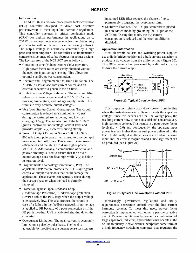
Application informationMost electronic ballasts and switching power supplies
use a diode bridge rectifier and a bulk storage capacitor toproduce a dc voltage from the utility ac line (Figure 20).This DC voltage is then processed by additional circuitryto drive the desired output.
Figure 20. Typical Circuit without PFC
Load
ConverterRectifiers
BulkStorage
Capacitor
+
ACLine
This simple rectifying circuit draws power from the linewhen the instantaneous ac voltage exceeds the capacitorvoltage. Since this occurs near the line voltage peak, theresulting current draw is non sinusoidal and contains a veryhigh harmonic content. This results in a poor power factor(typically < 0.6) and consequently, the apparent inputpower is much higher than the real power delivered to theload. Additionally, if multiple devices are tied to the sameinput line, the effect is magnified and a “line sag” effect canbe produced (see Figure 21).
Figure 21. Typical Line Waveforms without PFC
Line Sag
Rectified DC
AC Line Voltage
AC Line Current
0
0
Vpk
Increasingly, government regulations and utilityrequirements necessitate control over the line currentharmonic content. To meet this need, power factorcorrection is implemented with either a passive or activecircuit. Passive circuits usually contain a combination oflarge capacitors, inductors, and rectifiers that operate at theac line frequency. Active circuits incorporate some form ofa high frequency switching converter that regulates the

NCP1607
www.onsemi.com10
input current to stay in phase with the input voltage. Thesecircuits operate at a higher frequency and so they aresmaller, lighter in weight, and more efficient than a passivecircuit. With proper control of an active PFC stage, almostany complex load can be made to appear in phase with theac line, thus significantly reducing the harmonic current
content. Because of these advantages, active PFC circuitshave become the most popular way to meet harmoniccontent requirements. Generally, they consist of insertinga PFC pre−regulator between the rectifier bridge and thebulk capacitor (Figure 22).
Figure 22. Active PFC Pre−Converter with the NCP1607
Rectifiers
+AC Line High
FrequencyBypassCapacitor
NCP1607
PFC Preconverter Converter
Load+ Bulk
StorageCapacitor
The boost (or step up) converter is the most populartopology for active power factor correction. With theproper control, it produces a constant voltage whiledrawing a sinusoidal current from the line. For mediumpower (<300 W) applications, critical conduction mode(also called borderline conduction mode) is the preferredcontrol method. Critical conduction mode (CRM) occurs atthe boundary between discontinuous conduction mode
(DCM) and continuous conduction mode (CCM). In CRM,the next driver on time is initiated when the boost inductorcurrent reaches zero. CRM operation is an ideal choice formedium power PFC boost stages because it combines thelower peak currents of CCM operation with the zero currentswitching of DCM operation. The operation andwaveforms in a PFC boost converter are illustrated inFigure 23.
Figure 23. Schematic and Waveforms of an Ideal CRM Boost Converter
Diode Bridge
IN
+
−
L
Diode Bridge
IN
+
−
L+
The power switch is ON The power switch is OFF
Critical Conduction Mode:Next current cycle starts assoon as the core is reset.
CoilCurrent
+
With the power switch voltage being about zero, theinput voltage is applied across the coil. The coil currentlinearly increases with a (VIN/L) slope.
The coil current flows through the diode. The coil voltage is (VOUT −VIN) and the coil current linearly decays with a (VOUT − VIN)/L slope.
VOUT
(VOUT − VIN)/L
IL(pk)
ILVIN
Vdrain
Vdrain
VIN/L
VOUT
VIN
If next cycle does not startthen Vdrain rings towards VIN
+
ILVIN Vdrain

NCP1607
www.onsemi.com11
When the switch is closed, the inductor current increaseslinearly to its peak value. When the switch opens, theinductor current linearly decreases to zero. At this point,the drain voltage of the switch (Vd) is essentially floatingand begins to drop. If the next switching cycle does notstart, then the voltage will ring with a dampened frequencyaround Vin. A simple derivation of equations (such as foundin AND8123), leads to the result that good power factorcorrection in CRM operation is achieved when the on timeis constant across an ac cycle and is equal to:
ton �2 � POUT � L
� � Vac2 (eq. 1)
A simple plot of this switching over an ac line cycle isillustrated in Figure 24. The off time varies based on theinstantaneous line voltage, but the on time is kept constant.This naturally causes the peak inductor current (IL(pk)) tofollow the ac line voltage.
The NCP1607 represents an ideal method to implementthis constant on time CRM control in a cost effective androbust solution. The device incorporates an accurateregulation circuit, a low power startup circuit, andadvanced protection features.
Figure 24. Inductor Waveform During CRM Operation
ON
OFFMOSFET
IIN(t)
IL(t)
VIN(t)VIN(pk)
IL(pk)
IIN(pk)
ERROR AMPLIFIER REGULATIONThe NCP1607 is configured to regulate the boost output
voltage based on its built in error amplifier (EA). The erroramplifier ’s negative terminal is pinned out to FB, thepositive terminal is tied to a 2.5 V ± 1.6% reference, and theoutput is pinned out to Control (Figure 25).
Figure 25. Error Amplifier and On Time Regulation Circuits
FB
Control
+−
EA+
PWM BLOCK
VCONTROL
ROUT2
ROUT1
CCOMP
tPWM
ton(MAX)
VOUT
ton
VEAL VEAH
Slope � CtICHARGE
VCONTROL
RFBVREF
A resistor divider from the boost output to the input of theEA sets the FB level. If the output voltage is too low, thenthe FB level will drop and the EA will cause the controlvoltage to increase. This increases the on time of the driver,which increases the power delivered and brings the outputback into regulation. Alternatively, if the output voltage(and hence FB voltage) is too high, then the control leveldecreases and the driver on times are shortened. In this way,the circuit regulates the output voltage (VOUT) so that theVOUT portion that is applied to FB through the resistor
divider ROUT1 and ROUT2 is equal to the internal reference(2.5 V). The output voltage is set using Equation 2:
VOUT � VREF � �ROUT1 � REQ
REQ
� (eq. 2)
Where REQ is the parallel combination of ROUT2 and RFB.REQ is calculated using Equation 3:
REQ �ROUT2 � RFB
ROUT2 � RFB
(eq. 3)

NCP1607
www.onsemi.com12
A compensation network is placed between the FB andControl pins to reduce the speed at which the EA respondsto changes in the boost output. This is necessary due to thenature of an active PFC circuit. The PFC stage absorbs asinusoidal current from a sinusoidal line voltage. Hence,the converter provides the load with a power that matchesthe average demand only. Therefore, the output capacitormust “absorb” the difference between the delivered power
and the power consumed by the load. This means that whenthe power fed to the load is lower than the demand, theoutput capacitor discharges to compensate for the lack ofpower. Alternatively, when the supplied power is higherthan that absorbed by the load, the output capacitor chargesto store the excess energy. The situation is depicted inFigure 26.
Figure 26. Output Voltage Ripple for a Constant Output Power
VOUT
POUT
PIN
Iac
Vac
As a consequence, the output voltage exhibits a ripple ata frequency of either 100 Hz (for 50 Hz mains such as inEurope) or 120 Hz (for 60 Hz mains in the USA). Thisripple must not be taken into account by the regulation loopbecause the error amplifier’s output voltage must be keptconstant over a given ac line cycle for a proper shaping ofthe line current. Due to this constraint, the regulationbandwidth is typically set below 20 Hz. For a simple type 1compensation network, only a capacitor is placed betweenFB and Control (see Figure 1). In this configuration, thecapacitor necessary to attenuate the bulk voltage ripple isgiven by:
CCOMP �10
G20
4 � � fline � ROUT1(eq. 4)
where G is the attenuation level in dB (commonly 60 dB)
ON TIME SEQUENCESince the NCP1607 is designed to control a CRM boost
converter, its switching pattern must accommodateconstant on times and variable off times. The Controllergenerates the on time via an external capacitor connectedto pin 3 (Ct). A current source charges this capacitor to alevel determined by the Control pin voltage. Specifically,Ct is charged to VCONTROL minus the VEAL offset (2.1 Vtypical). Once this level is exceeded, the drive is turned off(Figure 27).
Figure 27. On Time Generation
Control
Ct +−
PWM
+
DRV
ICHARGE
ton
VEAL
VCONTROL − VEAL
ton
VCt
VCt(off)
VDD
DRV
VCONTROL
Since VCONTROL varies with the RMS line level andoutput load, this naturally satisfies equation 1. And if thevalues of compensation components are sufficient to filter

NCP1607
www.onsemi.com13
out the bulk voltage ripple, then this on time is trulyconstant over the ac line cycle.
Note that the maximum on time of the controller occurswhen VCONTROL is at its maximum. Therefore, the Ctcapacitor must be sized to ensure that the required on timecan be delivered at full power and the lowest input voltagecondition. The maximum on time is given by:
ton(MAX) �Ct � VCTMAX
ICHARGE(eq. 5)
Combining this equation with equation 1, gives:
Ct �2 � POUT � L � ICHARGE
� � Vac 2 � VCTMAX(eq. 6)
where VCTMAX = 2.9 V (min)ICHARGE = 297 �A (max)
OFF TIME SEQUENCEWhile the on time is constant across the ac cycle, the off
time in CRM operation varies with the instantaneous inputvoltage. The NCP1607 determines the correct off time bysensing the inductor voltage. When the inductor currentdrops to zero, the drain voltage (“Vdrain” in Figure 23) isessentially floating and naturally begins to drop. If theswitch is turned on at this moment, then CRM operationwill be achieved. To measure this high voltage directly onthe inductor is generally not economical or practical.Rather, a smaller winding is taken off of the boost inductor.This winding, called the zero current detector (ZCD)winding, gives a scaled version of the inductor output andis more useful to the controller.
Figure 28. Voltage Waveforms for Zero CurrentDetection
DRV
Winding
Drain
VOUT
VCL(POS)VZCDHVZCDL
ZCDVCL(NEG)
VZCD(on)
VZCD(off)
Figure 28 gives typical operating waveforms with theZCD winding. When the drive is on, a negative voltageappears on the ZCD winding. And when the drive is off, apositive voltage appears. When the inductor current dropsto zero, then the ZCD voltage falls and starts to ring aroundzero volts. The NCP1607 detects this falling edge and startsthe next driver on time. To ensure that a ZCD event hastruly occurred, the NCP1607’s logic (Figure 29) waits forthe ZCD pin voltage to rise above VZCDH (2.1 V typical)and then fall below VZCDL (1.6 V typical). In this way,CRM operation is easily achieved.
Figure 29. Implementation of the ZCD Winding
ZCD
+−
+
+−+
VCL(POS)Clamp
Shutdown
Demag
VCL(NEG)Active Clamp
+−
+
Reset Dominant
LatchR
QS
DRIVE
RSENSE
RZCD
VDD
Vin
NZCD
Q
NB
VZCDH
VZCDL
VSDL

NCP1607
www.onsemi.com14
To prevent negative voltages on the ZCD pin, the pin isinternally clamped to VCL(NEG) (600 mV typical) when theZCD winding is negative. Similarly, the ZCD pin isclamped to VCL(POS) (5.7 V typical), when the voltage risestoo high. Because of these clamps, a resistor (RZCD inFigure 29) is necessary to limit the current from the ZCDwinding to the ZCD pin.
At startup, there is no energy in the ZCD winding andtherefore no voltage signal to activate the ZCDcomparators. This means that the driver could never turnon. Therefore, to enable the PFC stage to startup underthese conditions, an internal watchdog timer is integratedinto the controller. This timer turns the drive on if the driverhas been off for more than 180 �s (typical). This feature isdeactivated during a fault mode (OVP, UVP, or Shutdown),and reactivated when the fault is removed.
STARTUPGenerally, a resistor connected between the ac input and
VCC (pin 8) charges the VCC capacitor to the VCC(on) level(12 V typical). Because of the very low consumption of theNCP1607 during this stage (< 40 �A), most of the currentgoes directly to charging up the VCC capacitor. Thisprovides faster startup times and reduced standby powerdissipation. When the VCC voltage exceeds the VCC(on)
level, the internal references and logic of the NCP1607 turnon. The controller has an undervoltage lockout (UVLO)feature which keeps the part active until VCC drops belowVCC(off) (9.5 V typical). This hysteresis allows ample timefor the auxiliary winding to take over and supply thenecessary power to VCC (Figure 30).
Figure 30. Typical VCC Startup Waveform
VCCVCC(on)
VCC(off)
When the PFC pre−converter is loaded by a switch modepower supply (SMPS), then it is often preferable to have theSMPS controller startup first. The SMPS can then supplythe NCP1607 VCC directly. Advanced controllers, such asthe NCP1230 or NCP1381, can control when to turn on thePFC stage (see Figure 31) leading to optimal systemperformance. This setup also eliminates the startupresistors and therefore improves the no load powerdissipation of the system.
Figure 31. NCP1607 Supplied by a Downstream SMPS Controller (NCP1230)
1
7
6
5
2
3
4
NC
P16
07
++
+
+
1
7
6
5
2
3
4
NCP1230
8 8
VCC
+
CBULK
DBOOST
PFC_VCC
QUICK START and SOFT STARTAt startup, the error amplifier is enabled and Control is
pulled up to VEAL (2.1 V typical). This is the lowest levelof control voltage which produces output drives. Thisfeature, called “quick start,” eliminates the delay at startup
associated with charging the compensation network to itsminimum level. This also produces a natural “soft−start”mode where the controller’s power ramps up from zero tothe required power (see Figure 32).
NCP1607
www.onsemi.com15
Figure 32. Startup Timing Diagram Showing theNatural Soft Start of the Control Pin
FB
Control
Natural Soft Start
VCC
IM
VEAL
VOUT
VCC(off)
VCC(on)
VREF
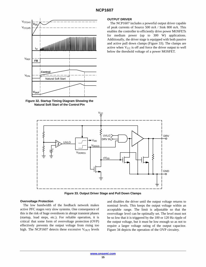
OUTPUT DRIVERThe NCP1607 includes a powerful output driver capable
of peak currents of Source 500 mA / Sink 800 mA. Thisenables the controller to efficiently drive power MOSFETsfor medium power (up to 300 W) applications.Additionally, the driver stage is equipped with both passiveand active pull down clamps (Figure 33). The clamps areactive when VCC is off and force the driver output to wellbelow the threshold voltage of a power MOSFET.
Figure 33. Output Driver Stage and Pull Down Clamps
UVLO
DRV
GND
+−
+
DRV IN
uVDD
VCC
VDD
VDDGD
VDDREG
UVLO
Overvoltage ProtectionThe low bandwidth of the feedback network makes
active PFC stages very slow systems. One consequence ofthis is the risk of huge overshoots in abrupt transient phases(startup, load steps, etc.). For reliable operation, it iscritical that some form of overvoltage protection (OVP)effectively prevents the output voltage from rising toohigh. The NCP1607 detects these excessive VOUT levels
and disables the driver until the output voltage returns tonominal levels. This keeps the output voltage within anacceptable range. The limit is adjustable so that theovervoltage level can be optimally set. The level must notbe so low that it is triggered by the 100 or 120 Hz ripple ofthe output voltage, but it must be low enough so as not torequire a larger voltage rating of the output capacitor.Figure 34 depicts the operation of the OVP circuitry.

NCP1607
www.onsemi.com16
Figure 34. OVP and UVP Circuit Blocks
FB
Control
+−
E/A
+−
Measure
+
+
UVP
Fault
Dynamic OVP
VEAHClamp
Static OVP is triggeredwhen clamp is activated.
VEALClamp
Static OVP
Enable
(Enable EA)
ROUT2
ROUT1
CCOMPVDD
ICONTROL > Iovp
ICONTROL
VOUT
ICONTROL
VCONTROL
RFB
IROUT1
IROUT2
VREF
VUVP
IRFB
When the output voltage is in steady state equilibrium,ROUT1 and ROUT2 regulate the FB voltage to VREF. Duringthis equilibrium state, no current flows through thecompensation capacitor (CCOMP shown in Figure 34).These facts allow the following equations to be derived:• The ROUT1 current is:
IROUT1 �VOUT � VREF
ROUT1(eq. 7)
• The REQ current is:
IEQ �VREF
REQ
� IROUT2 � IFB (eq. 8)
• And since no current flows through CCOMP,
IROUT1 �VOUT � VREF
ROUT1
�VREF
REQ
(eq. 9)
Under stable conditions, Equations 7 through 9 are true.Conversely, when VOUT is not at the target voltage, theoutput of the error amplifier sinks or sources the currentnecessary to maintain VREF on pin 1.
In the case of an overvoltage condition:• The error amplifier maintains VREF on pin 1, and the
REQ current remains the same as the steady statevalue:
IEQ �VREF
REQ(eq. 10)
• The ROUT1 current is increased and is calculated usingEquation 11:
IROUT1 �VOUT(OVP) � VREF
ROUT1
�VOUT � �VOUT � VREF
ROUT1 (eq. 11)
where �VOUT is the output voltage excess.• The error amplifier sinks:
IControl � IROUT1 � IEQ �VOUT � �VOUT � VREF
ROUT1
�VREF
REQ
(eq. 12)
The combination of Equations 2 and 12 yield a simpleexpression of the current sunk by the error amplifier:
ICONTROL ��VOUT
ROUT1
The current absorbed by pin 2 (IControl) is proportional tothe output voltage excess. The circuit senses this currentand disables the drive (pin 7) when IControl exceeds IOVP(10.4 �A typical). The OVP threshold is calculated usingEquation 13.
VOUT(OVP) � VOUT � ROUT1 � IOVP (eq. 13)
The OVP limit is set by adjusting ROUT1. ROUT1 iscalculated using Equation 14.
ROUT1 �VOUT(OVP) � VOUT
IOVP
(eq. 14)
For example, if 440 V is the maximum output voltageand 400 V is the target output voltage, then ROUT1 iscalculated using Equation 14.
ROUT1 � 440 � 40010.4�
� 3.846 M�
If ROUT1 is selected as 4 M�,, then VOUT(OVP) = 442 V.

NCP1607
www.onsemi.com17
STATIC OVERVOLTAGE PROTECTIONIf the OVP condition lasts for a long time, it may happen
that the error amplifier output reaches its minimum level(i.e. Control = VEAL). It would then not be able to sink anycurrent and maintain the OVP fault. Therefore, to avoid anydiscontinuity in the OVP disabling effect, the circuitincorporates a comparator which detects when the lowerlevel of the error amplifier is reached. This event, called“static OVP”, disables the output drives. Once the OVPevent is over, and the output voltage has dropped to normal,then Control rises above the lower limit and the driver isre−enabled (Figure 35).
Figure 35. OVP Timing Diagram
Dynamic OVP
Static OVP
DRV
IOVPH
IOVPL
VEAH VCONTROL
VOUT
VEAL
ICONTROL
NCP1607 Undervoltage Protection (UVP)When the PFC stage is plugged in, the output voltage is
forced to roughly equate the peak line voltage. TheNCP1607 detects an undervoltage fault when this outputvoltage is unusually low, such that the feedback voltage isbelow VUVP (300 mV typical). In an UVP fault, the driveoutput and error amplifier (EA) are disabled. The latter isdone so that the EA does not source a current which wouldincrease the FB voltage and prevent the UVP event frombeing accurately detected. The UVP feature helps toprotect the application if something is wrong with thepower path to the bulk capacitor (i.e. the capacitor cannotcharge up) or if the controller cannot sense the bulk voltage(i.e. the feedback loop is open).
Furthermore, the NCP1607 incorporates a novel startupsequence which ensures that undervoltage conditions arealways detected at startup. It accomplishes this by waitingapproximately 180 �s after VCC reaches VCC(on) beforeenabling the error amplifier (Figure 36). During this waittime, it looks to see if the feedback (FB) voltage is greaterthan the UVP threshold. If not, then the controller enters aUVP fault and leaves the error amplifier disabled.
However, if the FB pin voltage increases and exceeds theUVP level, then the controller will start the application upnormally.
Figure 36. The NCP1607’s Startup Sequence withand without a UVP Fault
FB
Control
2.5 V
UVP
UVP WaitUVP Wait
VUVP
VEAH
VEAL
VOUT
VOUT
VCC(off)
VCC(on)VCC
UVP Fault is “Removed”
The voltage on the output which exits a UVP fault isgiven by:
VOUT(UVP) �ROUT1 � REQ
REQ� VUVP (eq. 15)
If ROUT1 = 4 M� and REQ = 25.16 k�, then the VOUTUVP threshold is 48 V. This corresponds to an input voltageof approximately 34 Vac.
Open Feedback Loop ProtectionThe NCP1607 features comprehensive protection
against open feedback loop conditions by including OVP,UVP, and Floating Pin Protection (FPP). Figure 37illustrates three conditions in which the feedback loop isopen. The corresponding number below describes eachcondition shown in Figure 37.
1. UVP Protection: The connection from resistorROUT1 to the FB pin is open. ROUT2 pulls downthe FB pin to ground. The UVP comparatordetects a UVP fault and the drive is disabled.
2. OVP Protection: The connection from resistorROUT2 to the FB pin is open. ROUT1 pulls up theFB pin to the output voltage. The ESD diodeclamps the FB voltage to 10 V and ROUT1 limitsthe current into the FB pin. The VEAL clampdetects a static OVP fault and the drive isdisabled.
3. FPP Protection: The FB pin is floating. Theinternal pulldown resistor RFB pulls down the FBvoltage below the UVP threshold. The UVPcomparator detects a UVP fault and the drive isdisabled.

NCP1607
www.onsemi.com18
UVP and OVP protect the system from low bulk voltagesand rapid operating point changes respectively, while theFPP protects the system against floating feedback pinconditions. If FPP is not implemented and a manufacturingerror causes the feedback pin to float, then the feedbackvoltage is dependent on the coupling within the system andthe surrounding environment. The coupled feedbackvoltage may be within the regulation limits (i.e. above theUVP threshold, but below VREF) and cause the controllerto deliver excessive power. The result is that the outputvoltage rises until a component fails due to the voltagestress.
The tradeoff for including FPP is that the value of RFBcauses an error in the output voltage. The output voltageincluding the error caused by RFB (VOUT) is calculatedusing Equation 16:
VOUT � VOUT � ROUT1 �VREF
RFB
(eq. 16)
Using the values from the OVP calculation, the outputvoltage including the error caused by RFB is equal to:
VOUT � 400 � 4 M �2.5
4.7 M� 402 V
The error caused by RFB is compensated by adjustingROUT2. The parallel combination of RFB and ROUT2 forman equivalent resistor REQ that is calculated usingEquation 17.
REQ � ROUT1 �VREF
VOUT � VREF
(eq. 17)
REQ � 4 M �2.5
400 � 2.5� 25.16 k�
REQ is used to calculate ROUT2.
ROUT2 �REQ � RFB
RFB � REQ
(eq. 18)
ROUT2 �25.16 k � 4.7 M
4.7 M � 25.16 k� 25.29 k�
The compensated output voltage is calculated usingEquation 19.
VOUT � VREF � �ROUT1 � ROUT2
ROUT2�� ROUT1 �
VREF
RFB
(eq. 19)
VOUT � 2.5 � �4 M� 25.29 k
25.29 k�� 4 M �
2.5
4.7 M� 400 V
Control
E/AFB
UVP
Static OVP
Fault
Dynamic OVP
Enable
Condition 2
Condition 1Condition 3
Figure 37. Open Feedback Loop Protection
+-
+
+-
+RFB
CCOMP
VCONTROL
ICONTROL
ICONTROLROUT2
ROUT1
VOUT
VEAHClamp
VDD
VEALClamp
Measure
Static OVP is triggeredwhen clamp is activated
(Enable EA)
ICONTROL > Iovp
VREF
VUVP
Overcurrent Protection (OCP)A dedicated pin on the NCP1607 senses the peak current
and limits the driver on time if this current exceedsVCS(limit). This level is 0.5 V (typical). Therefore, themaximum peak current can be adjusted by changing RSENSEaccording to:
Ipeak �VCS(limit)
RS(eq. 20)
An internal LEB filter (Figure 38) reduces the likelihoodof switching noise falsely triggering the OCP limit. Thisfilter blanks out the first 250 ns (typical) of the currentsense signal. If additional filtering is necessary, a small RCfilter can be added between RSENSE and the CS pin.

NCP1607
www.onsemi.com19
Figure 38. OCP Circuitry with Optional External RCFilter
CS+−+
OCPLEB
DRV
optionalRS
VCS(limit)
SHUTDOWN MODEThe NCP1607 allows for two methods to place the
controller into a standby mode of operation. The FB pin canbe pulled below the UVP level (300 mV typical) or the ZCDpin can be pulled below the VSDL level (200 mV typical).If the FB pin is used for shutdown (Figure 39(a)), care mustbe taken to ensure that no significant leakage current existson the shutdown circuitry. This could impact the outputvoltage regulation. If the ZCD pin is used for shutdown(Figure 39(b)), then any parasitic capacitance created bythe shutdown circuitry will add to the delay in detecting thezero inductor current event.
Figure 39. Shutting Down the PFC Stage by Pulling FB to GND (A) or Pulling ZCD to GND (B)
1
4
3
2
8
5
6
7
NCP1607
Shutdown
Shutdown
RZCD
ROUT2
ROUT1
VOUT
CCOMP
1
4
3
2
8
5
6
7
NCP1607
Figure 39(a) Figure 39(b)
LBOOST
FB
Control
Ct
CS
GND
ZCD
DRV
VCCFB
Control
Ct
CS
GND
ZCD
DRV
VCC
To activate the shutdown feature on ZCD, the internalclamp must first be overcome. This clamp will draw amaximum of ICL(NEG) (5.0 mA maximum) before releasingand allowing the ZCD pin voltage to drop low enough toshutdown the part (Figure 40). After shutdown, the
comparator includes approximately 90 mV of hysteresis toensure noise free operation. A small current source (70 �Atypical) is also activated to pull the unit out of the shutdowncondition when the external pull down is released.
Figure 40. Shutdown Comparator and Current Draw to Overcome Negative Clamp
Shutdown
5 mA
~1 VVSDL VSDH
IZCD
VCL(NEG)
~70 �A
Controller Disabled
Controller Enabled

NCP1607
www.onsemi.com20
Application InformationON Semiconductor provides an electronic design tool, a
demonstration board and an application note to facilitatethe design of the NCP1607 and reduce development cycletime. All the tools can be downloaded or ordered atwww.onsemi.com.
The electronic design tool allows the user to easilydetermine most of the system parameters of a boostpre−converter. The demonstration board is a boostpre−converter that delivers 100 W at 400 V. The circuitschematic is shown in Figure 41. The pre−converter designis described in Application Note AND8353/D.
Figure 41. Application Board Circuit Schematic
C3 D1
+
+
U1NCP1607
5ZCD
3 Ct 6GND4 CS
8VCC7DRV
1 FB
2 Control
J3
J1
L2
F1
C2
Q1
BRIDGE
t
NTC
J2
L1R1
C1
RSTART1 RSTART2
LBOOST DBOOST
CVCCDAUX DVCC
RZCD
CVCC
2
DDRV
RDRV
CZCD
RCTUP2
RCTUP1 RO1A
RO1B
CBUL-
K
ROUT2B ROUT2A
CIN
CCOMP1RCOMP2
CCOMP
CT1CT2 CCS
RCS RS3 RS2 RS1
RCT

NCP1607
www.onsemi.com21
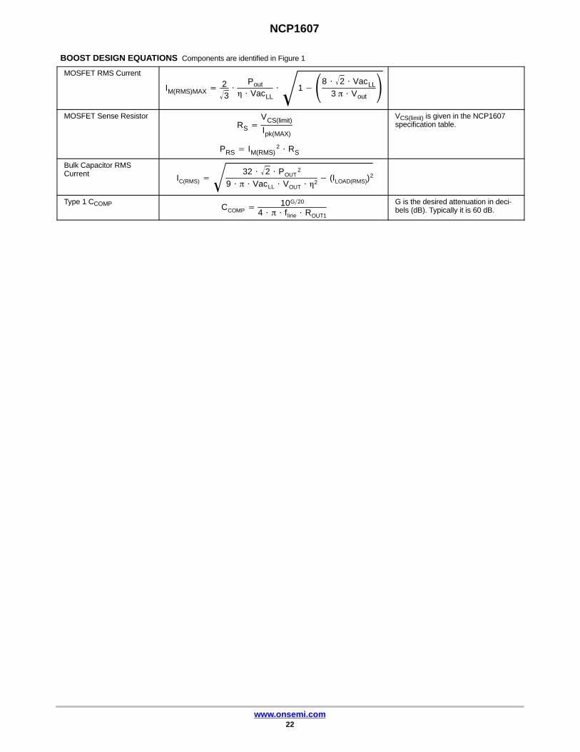
BOOST DESIGN EQUATIONS Components are identified in Figure 1
RMS Input CurrentIac �
POUT� � Vac
� (the efficiency of only the BoostPFC stage) is generally in the rangeof 90 − 95%
Maximum Inductor PeakCurrent Ipk(MAX) �
2 � 2 � POUT� � VacLL
Where VacLL is the minimum line in-put voltage. Ipk(MAX) occurs at thelowest line voltage.
Inductor Value
L 2 � Vac2 � �VOUT
2� Vac�
VOUT � Vac � Ipk(MAX) � fSW(min)
fSW(MIN) is the minimum desiredswitching frequency. The maximum Lmust be calculated at low line andhigh line.
Maximum On Timeton(MAX) �
2 � L � POUT
� � VacLL2
The maximum on time occurs at thelowest line voltage and maximumoutput power.
Off Time
toff �ton
VOUT
Vac��sin(�)�� 2� 1
The off time is greatest at the peak ofthe ac line voltage and approacheszero at the ac line zero crossings.Theta (�) represents the angle of theac line voltage.
Frequency
fSW �Vac 2 � �
2 � L � POUT� �1 �
Vac � |sin �| � 2
VOUT�
Pin 3 CapacitorCt �
2 � POUT � L � ICHARGE
� � Vac 2 � VCTMAX
ICHARGE and VCTMAX are given inthe NCP1607 specification table.
Boost Turns to ZCD TurnsRatio
NB : NZCD VOUT � VacHL � 2
VZCDH
Where VacHL is the maximum lineinput voltage. The turns ratio must below enough so as to trigger the ZCDcomparators at high line.
Resistor from ZCD wind-ing to the ZCD pin (pin 5) RZCD �
VacHL � 2
ICL(NEG) � (NB : NZCD)
RZCD must be large enough so thatthe shutdown comparator is not inad-vertently activated.
Boost Output VoltageVOUT � VREF �
ROUT1 � REQREQ
REQ �ROUT2 � RFB
ROUT2 � RFB
Maximum VOUT voltageprior to OVP activation andthe necessary ROUT1 andROUT2.
VOUT(OVP) � VOUT ��IOVP � ROUT1�
ROUT1 �VOUT(OVP) � VOUT
IOVP
REQ � ROUT1 �VREF
VOUT � VREF
ROUT2 �REQ � RFB
RFB � REQ
IOVP is given in the NCP1607 spe-cification table.
Minimum output voltagenecessary to exit under-voltage protection (UVP)
VOUT(UVP) � VUVP �ROUT1 � REQ
REQ
VUVP is given in the NCP1607 spe-cification table.
Bulk Cap RippleVripple(pk−pk) �
POUTCBULK � 2 � � � fline � VOUT
Use fline = 47 Hz for worst case atuniversal lines. The ripple must notexceed the OVP level for VOUT.
Inductor RMS CurrentIL(RMS) �
2 � POUT
3 � VacLL � �
Boost Diode RMS CurrentID(RMS)MAX � 4
3� 2 � 2
� �
POUT
� � VacLL � VOUT
NCP1607
www.onsemi.com22
BOOST DESIGN EQUATIONS Components are identified in Figure 1
MOSFET RMS Current
IM(RMS)MAX � 23�
Pout� � VacLL
� 1 ��8 � 2 � VacLL3 � � Vout
�MOSFET Sense Resistor
RS �VCS(limit)
Ipk(MAX)
PRS � IM(RMS)2 � RS
VCS(limit) is given in the NCP1607specification table.
Bulk Capacitor RMSCurrent IC(RMS) �
32 � 2 � POUT2
9 � � � VacLL � VOUT � �2� (ILOAD(RMS))
2Type 1 CCOMP CCOMP � 10G�20
4 � � � fline � ROUT1
G is the desired attenuation in deci-bels (dB). Typically it is 60 dB.
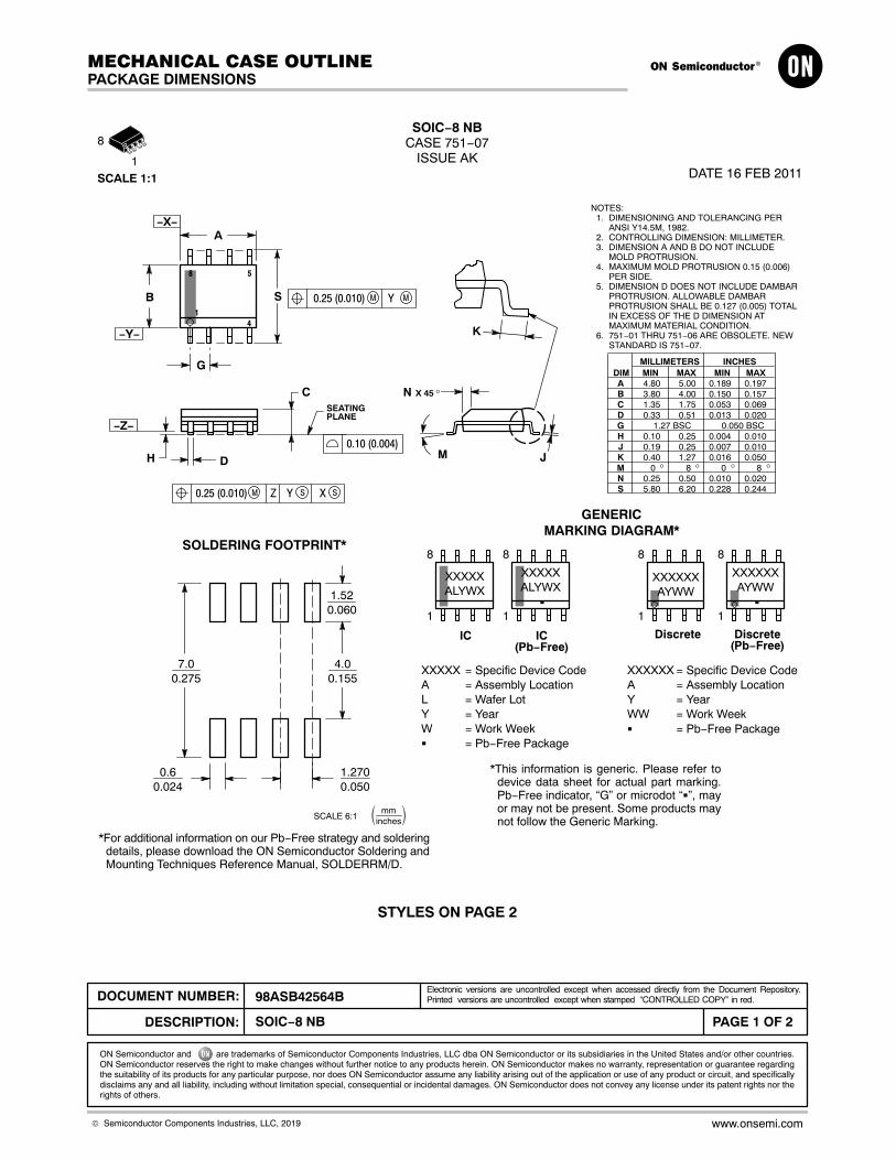
SOIC−8 NBCASE 751−07
ISSUE AKDATE 16 FEB 2011
SEATINGPLANE
14
58
N
J
X 45�
K
NOTES:1. DIMENSIONING AND TOLERANCING PER
ANSI Y14.5M, 1982.2. CONTROLLING DIMENSION: MILLIMETER.3. DIMENSION A AND B DO NOT INCLUDE
MOLD PROTRUSION.4. MAXIMUM MOLD PROTRUSION 0.15 (0.006)
PER SIDE.5. DIMENSION D DOES NOT INCLUDE DAMBAR
PROTRUSION. ALLOWABLE DAMBARPROTRUSION SHALL BE 0.127 (0.005) TOTALIN EXCESS OF THE D DIMENSION ATMAXIMUM MATERIAL CONDITION.
6. 751−01 THRU 751−06 ARE OBSOLETE. NEWSTANDARD IS 751−07.
A
B S
DH
C
0.10 (0.004)
SCALE 1:1
STYLES ON PAGE 2
DIMA
MIN MAX MIN MAXINCHES
4.80 5.00 0.189 0.197
MILLIMETERS
B 3.80 4.00 0.150 0.157C 1.35 1.75 0.053 0.069D 0.33 0.51 0.013 0.020G 1.27 BSC 0.050 BSCH 0.10 0.25 0.004 0.010J 0.19 0.25 0.007 0.010K 0.40 1.27 0.016 0.050M 0 8 0 8 N 0.25 0.50 0.010 0.020S 5.80 6.20 0.228 0.244
−X−
−Y−
G
MYM0.25 (0.010)
−Z−
YM0.25 (0.010) Z S X S
M� � � �
XXXXX = Specific Device CodeA = Assembly LocationL = Wafer LotY = YearW = Work Week� = Pb−Free Package
GENERICMARKING DIAGRAM*
1
8
XXXXXALYWX
1
8
IC Discrete
XXXXXXAYWW
�1
8
1.520.060
7.00.275
0.60.024
1.2700.050
4.00.155
� mminches
�SCALE 6:1
*For additional information on our Pb−Free strategy and solderingdetails, please download the ON Semiconductor Soldering andMounting Techniques Reference Manual, SOLDERRM/D.
SOLDERING FOOTPRINT*
Discrete
XXXXXXAYWW
1
8
(Pb−Free)
XXXXXALYWX
�1
8
IC(Pb−Free)
XXXXXX = Specific Device CodeA = Assembly LocationY = YearWW = Work Week� = Pb−Free Package
*This information is generic. Please refer todevice data sheet for actual part marking.Pb−Free indicator, “G” or microdot “�”, mayor may not be present. Some products maynot follow the Generic Marking.
MECHANICAL CASE OUTLINE
PACKAGE DIMENSIONS
ON Semiconductor and are trademarks of Semiconductor Components Industries, LLC dba ON Semiconductor or its subsidiaries in the United States and/or other countries.ON Semiconductor reserves the right to make changes without further notice to any products herein. ON Semiconductor makes no warranty, representation or guarantee regardingthe suitability of its products for any particular purpose, nor does ON Semiconductor assume any liability arising out of the application or use of any product or circuit, and specificallydisclaims any and all liability, including without limitation special, consequential or incidental damages. ON Semiconductor does not convey any license under its patent rights nor therights of others.
98ASB42564BDOCUMENT NUMBER:
DESCRIPTION:
Electronic versions are uncontrolled except when accessed directly from the Document Repository.Printed versions are uncontrolled except when stamped “CONTROLLED COPY” in red.
PAGE 1 OF 2SOIC−8 NB
© Semiconductor Components Industries, LLC, 2019 www.onsemi.com

SOIC−8 NBCASE 751−07
ISSUE AKDATE 16 FEB 2011
STYLE 4:PIN 1. ANODE
2. ANODE3. ANODE4. ANODE5. ANODE6. ANODE7. ANODE8. COMMON CATHODE
STYLE 1:PIN 1. EMITTER
2. COLLECTOR3. COLLECTOR4. EMITTER5. EMITTER6. BASE7. BASE8. EMITTER
STYLE 2:PIN 1. COLLECTOR, DIE, #1
2. COLLECTOR, #13. COLLECTOR, #24. COLLECTOR, #25. BASE, #26. EMITTER, #27. BASE, #18. EMITTER, #1
STYLE 3:PIN 1. DRAIN, DIE #1
2. DRAIN, #13. DRAIN, #24. DRAIN, #25. GATE, #26. SOURCE, #27. GATE, #18. SOURCE, #1
STYLE 6:PIN 1. SOURCE
2. DRAIN3. DRAIN4. SOURCE5. SOURCE6. GATE7. GATE8. SOURCE
STYLE 5:PIN 1. DRAIN
2. DRAIN3. DRAIN4. DRAIN5. GATE6. GATE7. SOURCE8. SOURCE
STYLE 7:PIN 1. INPUT
2. EXTERNAL BYPASS3. THIRD STAGE SOURCE4. GROUND5. DRAIN6. GATE 37. SECOND STAGE Vd8. FIRST STAGE Vd
STYLE 8:PIN 1. COLLECTOR, DIE #1
2. BASE, #13. BASE, #24. COLLECTOR, #25. COLLECTOR, #26. EMITTER, #27. EMITTER, #18. COLLECTOR, #1
STYLE 9:PIN 1. EMITTER, COMMON
2. COLLECTOR, DIE #13. COLLECTOR, DIE #24. EMITTER, COMMON5. EMITTER, COMMON6. BASE, DIE #27. BASE, DIE #18. EMITTER, COMMON
STYLE 10:PIN 1. GROUND
2. BIAS 13. OUTPUT4. GROUND5. GROUND6. BIAS 27. INPUT8. GROUND
STYLE 11:PIN 1. SOURCE 1
2. GATE 13. SOURCE 24. GATE 25. DRAIN 26. DRAIN 27. DRAIN 18. DRAIN 1
STYLE 12:PIN 1. SOURCE
2. SOURCE3. SOURCE4. GATE5. DRAIN6. DRAIN7. DRAIN8. DRAIN
STYLE 14:PIN 1. N−SOURCE
2. N−GATE3. P−SOURCE4. P−GATE5. P−DRAIN6. P−DRAIN7. N−DRAIN8. N−DRAIN
STYLE 13:PIN 1. N.C.
2. SOURCE3. SOURCE4. GATE5. DRAIN6. DRAIN7. DRAIN8. DRAIN
STYLE 15:PIN 1. ANODE 1
2. ANODE 13. ANODE 14. ANODE 15. CATHODE, COMMON6. CATHODE, COMMON7. CATHODE, COMMON8. CATHODE, COMMON
STYLE 16:PIN 1. EMITTER, DIE #1
2. BASE, DIE #13. EMITTER, DIE #24. BASE, DIE #25. COLLECTOR, DIE #26. COLLECTOR, DIE #27. COLLECTOR, DIE #18. COLLECTOR, DIE #1
STYLE 17:PIN 1. VCC
2. V2OUT3. V1OUT4. TXE5. RXE6. VEE7. GND8. ACC
STYLE 18:PIN 1. ANODE
2. ANODE3. SOURCE4. GATE5. DRAIN6. DRAIN7. CATHODE8. CATHODE
STYLE 19:PIN 1. SOURCE 1
2. GATE 13. SOURCE 24. GATE 25. DRAIN 26. MIRROR 27. DRAIN 18. MIRROR 1
STYLE 20:PIN 1. SOURCE (N)
2. GATE (N)3. SOURCE (P)4. GATE (P)5. DRAIN6. DRAIN7. DRAIN8. DRAIN
STYLE 21:PIN 1. CATHODE 1
2. CATHODE 23. CATHODE 34. CATHODE 45. CATHODE 56. COMMON ANODE7. COMMON ANODE8. CATHODE 6
STYLE 22:PIN 1. I/O LINE 1
2. COMMON CATHODE/VCC3. COMMON CATHODE/VCC4. I/O LINE 35. COMMON ANODE/GND6. I/O LINE 47. I/O LINE 58. COMMON ANODE/GND
STYLE 23:PIN 1. LINE 1 IN
2. COMMON ANODE/GND3. COMMON ANODE/GND4. LINE 2 IN5. LINE 2 OUT6. COMMON ANODE/GND7. COMMON ANODE/GND8. LINE 1 OUT
STYLE 24:PIN 1. BASE
2. EMITTER3. COLLECTOR/ANODE4. COLLECTOR/ANODE5. CATHODE6. CATHODE7. COLLECTOR/ANODE8. COLLECTOR/ANODE
STYLE 25:PIN 1. VIN
2. N/C3. REXT4. GND5. IOUT6. IOUT7. IOUT8. IOUT
STYLE 26:PIN 1. GND
2. dv/dt3. ENABLE4. ILIMIT5. SOURCE6. SOURCE7. SOURCE8. VCC
STYLE 27:PIN 1. ILIMIT
2. OVLO3. UVLO4. INPUT+5. SOURCE6. SOURCE7. SOURCE8. DRAIN
STYLE 28:PIN 1. SW_TO_GND
2. DASIC_OFF3. DASIC_SW_DET4. GND5. V_MON6. VBULK7. VBULK8. VIN
STYLE 29:PIN 1. BASE, DIE #1
2. EMITTER, #13. BASE, #24. EMITTER, #25. COLLECTOR, #26. COLLECTOR, #27. COLLECTOR, #18. COLLECTOR, #1
STYLE 30:PIN 1. DRAIN 1
2. DRAIN 13. GATE 24. SOURCE 25. SOURCE 1/DRAIN 26. SOURCE 1/DRAIN 27. SOURCE 1/DRAIN 28. GATE 1
ON Semiconductor and are trademarks of Semiconductor Components Industries, LLC dba ON Semiconductor or its subsidiaries in the United States and/or other countries.ON Semiconductor reserves the right to make changes without further notice to any products herein. ON Semiconductor makes no warranty, representation or guarantee regardingthe suitability of its products for any particular purpose, nor does ON Semiconductor assume any liability arising out of the application or use of any product or circuit, and specificallydisclaims any and all liability, including without limitation special, consequential or incidental damages. ON Semiconductor does not convey any license under its patent rights nor therights of others.
98ASB42564BDOCUMENT NUMBER:
DESCRIPTION:
Electronic versions are uncontrolled except when accessed directly from the Document Repository.Printed versions are uncontrolled except when stamped “CONTROLLED COPY” in red.
PAGE 2 OF 2SOIC−8 NB
© Semiconductor Components Industries, LLC, 2019 www.onsemi.com

onsemi, , and other names, marks, and brands are registered and/or common law trademarks of Semiconductor Components Industries, LLC dba “onsemi” or its affiliatesand/or subsidiaries in the United States and/or other countries. onsemi owns the rights to a number of patents, trademarks, copyrights, trade secrets, and other intellectual property.A listing of onsemi’s product/patent coverage may be accessed at www.onsemi.com/site/pdf/Patent−Marking.pdf. onsemi reserves the right to make changes at any time to anyproducts or information herein, without notice. The information herein is provided “as−is” and onsemi makes no warranty, representation or guarantee regarding the accuracy of theinformation, product features, availability, functionality, or suitability of its products for any particular purpose, nor does onsemi assume any liability arising out of the application or useof any product or circuit, and specifically disclaims any and all liability, including without limitation special, consequential or incidental damages. Buyer is responsible for its productsand applications using onsemi products, including compliance with all laws, regulations and safety requirements or standards, regardless of any support or applications informationprovided by onsemi. “Typical” parameters which may be provided in onsemi data sheets and/or specifications can and do vary in different applications and actual performance mayvary over time. All operating parameters, including “Typicals” must be validated for each customer application by customer’s technical experts. onsemi does not convey any licenseunder any of its intellectual property rights nor the rights of others. onsemi products are not designed, intended, or authorized for use as a critical component in life support systemsor any FDA Class 3 medical devices or medical devices with a same or similar classification in a foreign jurisdiction or any devices intended for implantation in the human body. ShouldBuyer purchase or use onsemi products for any such unintended or unauthorized application, Buyer shall indemnify and hold onsemi and its officers, employees, subsidiaries, affiliates,and distributors harmless against all claims, costs, damages, and expenses, and reasonable attorney fees arising out of, directly or indirectly, any claim of personal injury or deathassociated with such unintended or unauthorized use, even if such claim alleges that onsemi was negligent regarding the design or manufacture of the part. onsemi is an EqualOpportunity/Affirmative Action Employer. This literature is subject to all applicable copyright laws and is not for resale in any manner.
PUBLICATION ORDERING INFORMATIONTECHNICAL SUPPORTNorth American Technical Support:Voice Mail: 1 800−282−9855 Toll Free USA/CanadaPhone: 011 421 33 790 2910
LITERATURE FULFILLMENT:Email Requests to: [email protected]
onsemi Website: www.onsemi.com
Europe, Middle East and Africa Technical Support:Phone: 00421 33 790 2910For additional information, please contact your local Sales Representative
◊