Operational Amplifier, Low Voltage NCV5230 - onsemi
19
© Semiconductor Components Industries, LLC, 2010 February, 2020 − Rev. 6 1 Publication Order Number: NE5230/D Operational Amplifier, Low Voltage NCV5230 The NCV5230 is a very low voltage operational amplifier that can perform with a voltage supply as low as 1.8 V or as high as 15 V. In addition, split or single supplies can be used, and the output will swing to ground when applying the latter. There is a bias adjusting pin which controls the supply current required by the device and thereby controls its power consumption. If the part is operated at ±0.9 V supply voltages, the current required is only 110 mA when the current control pin is left open. Even with this low power consumption, the device obtains a typical unity gain bandwidth of 250 kHz. When the bias adjusting pin is connected to the negative supply, the unity gain bandwidth is typically 600 kHz while the supply current is increased to 600 mA. In this mode, the part will supply full power output beyond the audio range. The NCV5230 also has a unique input stage that allows the common−mode input range to go above the positive and below the negative supply voltages by 250 mV. This provides for the largest possible input voltages for low voltage applications. The part is also internally−compensated to reduce external component count. The NCV5230 has a low input bias current of typically ±40 nA, and a large open−loop gain of 125 dB. These two specifications are beneficial when using the device in transducer applications. The large open−loop gain gives very accurate signal processing because of the large “excess” loop gain in a closed−loop system. The output stage is a class AB type that can swing to within 100 mV of the supply voltages for the largest dynamic range that is needed in many applications. The NCV5230 is ideal for portable audio equipment and remote transducers because of its low power consumption, unity gain bandwidth, and 30 nV/ √ Hz noise specification. Features • Works Down to 1.8 V Supply Voltages • Adjustable Supply Current • Low Noise • Common−mode Includes Both Rails • V OUT Within 100 mV of Both Rails • These are Pb−Free Devices Applications • Portable Precision Instruments • Remote Transducer Amplifier • Portable Audio Equipment • Rail−to−Rail Comparators • Half−wave Rectification without Diodes • Remote Temperature Transducer with 4.0 to 20 mA Output Transmission www. onsemi.com PIN CONNECTIONS See detailed ordering and shipping information in the package dimensions section on page 15 of this data sheet. ORDERING INFORMATION (Top View) SOIC−8 D SUFFIX CASE 751 1 2 3 4 5 6 7 8 NC −IN +IN OUTPUT BIAS ADJ. V EE V CC NC − + N, D Packages 1 8 See general marking information in the device marking section on page 15 of this data sheet. DEVICE MARKING INFORMATION
-
Upload
khangminh22 -
Category
Documents
-
view
0 -
download
0
Transcript of Operational Amplifier, Low Voltage NCV5230 - onsemi

© Semiconductor Components Industries, LLC, 2010
February, 2020 − Rev. 61 Publication Order Number:
NE5230/D
Operational Amplifier, LowVoltage
NCV5230The NCV5230 is a very low voltage operational amplifier that can
perform with a voltage supply as low as 1.8 V or as high as 15 V.In addition, split or single supplies can be used, and the output willswing to ground when applying the latter. There is a bias adjusting pinwhich controls the supply current required by the device and therebycontrols its power consumption. If the part is operated at ±0.9 Vsupply voltages, the current required is only 110 �A when the currentcontrol pin is left open. Even with this low power consumption, thedevice obtains a typical unity gain bandwidth of 250 kHz. When thebias adjusting pin is connected to the negative supply, the unity gainbandwidth is typically 600 kHz while the supply current is increasedto 600 �A. In this mode, the part will supply full power output beyondthe audio range.
The NCV5230 also has a unique input stage that allows thecommon−mode input range to go above the positive and below thenegative supply voltages by 250 mV. This provides for the largestpossible input voltages for low voltage applications. The part is alsointernally−compensated to reduce external component count.
The NCV5230 has a low input bias current of typically ±40 nA, anda large open−loop gain of 125 dB. These two specifications arebeneficial when using the device in transducer applications. The largeopen−loop gain gives very accurate signal processing because of thelarge “excess” loop gain in a closed−loop system.
The output stage is a class AB type that can swing to within 100 mVof the supply voltages for the largest dynamic range that is needed inmany applications. The NCV5230 is ideal for portable audioequipment and remote transducers because of its low powerconsumption, unity gain bandwidth, and 30 nV/√Hz noisespecification.
Features• Works Down to 1.8 V Supply Voltages
• Adjustable Supply Current
• Low Noise
• Common−mode Includes Both Rails
• VOUT Within 100 mV of Both Rails
• These are Pb−Free Devices
Applications• Portable Precision Instruments
• Remote Transducer Amplifier
• Portable Audio Equipment
• Rail−to−Rail Comparators
• Half−wave Rectification without Diodes
• Remote Temperature Transducer with 4.0 to 20 mA OutputTransmission
www.onsemi.com
PIN CONNECTIONS
See detailed ordering and shipping information in the packagedimensions section on page 15 of this data sheet.
ORDERING INFORMATION
(Top View)
SOIC−8D SUFFIXCASE 751
1
2
3
4 5
6
7
8NC
−IN
+IN OUTPUT
BIAS ADJ.VEE
VCC
NC
−+
N, D Packages
1
8
See general marking information in the device markingsection on page 15 of this data sheet.
DEVICE MARKING INFORMATION

NCV5230
www.onsemi.com2
MAXIMUM RATINGS
Rating Symbol Value Unit
Single Supply Voltage VCC 18 V
Dual Supply Voltage VS ±9 V
Input Voltage (Note 1) VIN ±9 (18) V
Differential Input Voltage (Note 1) ±VS V
Common−Mode Voltage (Positive) VCM VCC + 0.5 V
Common−Mode Voltage (Negative) VCM VEE − 0.5 V
Power Dissipation (Note 2) PD 500 mW
Thermal Resistance, Junction−to−Ambient D Package R�JA 182 °C/W
Operating Junction Temperature (Note 2) TJ 150 °C
Operating Temperature Range TA −40 to 125 °C
80 Output Short−Circuit Duration to Either Power Supply Pin (Notes 2 and 3) Indefinite s
Storage Temperature Tstg −65 to 150 °C
Lead Soldering Temperature (10 sec max) Tsld 230 °C
Stresses exceeding those listed in the Maximum Ratings table may damage the device. If any of these limits are exceeded, device functionalityshould not be assumed, damage may occur and reliability may be affected.1. Can exceed the supply voltages when VS ≤ ±7.5 V (15 V).2. The maximum operating junction temperature is 150°C. At elevated temperatures, devices must be derated according to the package thermal
resistance and device mounting conditions. Derate above 25°C at the following rates:
D package at 5.5 mW/°C.3. Momentary shorts to either supply are permitted in accordance to transient thermal impedance limitations determined by the package and
device mounting conditions.
RECOMMENDED OPERATING CONDITIONS
Characteristic Value Unit
Single Supply Voltage 1.8 to 15 V
Dual Supply Voltage ±0.9 to ±7.5 V
Common−Mode Voltage (Positive) VCC + 0.25 V
Common−Mode Voltage (Negative) VEE − 0.25 V
Temperature −40 to +125 °C

NCV5230
www.onsemi.com3
DC AND AC ELECTRICAL CHARACTERISTIC Unless otherwise specified, ±0.9V ≤ Vs ≤ ±7.5 V or equivalent single supply,RL = 10 k�, full input common−mode range, over full operating temperature range.
Characteristic Symbol Test Conditions Bias Min Typ Max Unit
NCV5230
Offset Voltage VOS TA = 25°C Any 0.4 3.0 mV
TA = Tlow to Thigh Any 3.0 4.0
Drift VOS Any 2.0 5.0 �V/°C
Offset Current IOSTA = 25°C
High 3.0 50 nA
Low 3.0 30
TA = Tlow to Thigh
High 100
Low 60
Drift IOS High 0.5 1.4 nA/°C
Low 0.3 1.4
Bias Current IBTA = 25°C
High 40 150 nA
Low 20 60
TA = Tlow to Thigh
High 300
Low 300
Drift IB High 2.0 4.0 nA/°C
Low 2.0 4.0
Supply Current IS
VS = ±0.9 V
TA = 25°CLow 110 160 �A
High 600 750
TA = Tlow to Thigh
Low 275
High 850
VS = ±7.5 V
TA = 25°CLow 320 550 �A
High 1100 1600
TA = Tlow to Thigh
Low 600
High 1700
Common−Mode Input Range VCM VOS ≤ 6 mV, TA = 25°C Any V− − 0.25 V+ + 0.25 V
VOS ≤ 20 mV, TA = Tlow to Thigh Any V− V+
Common−Mode Rejection Ratio CMRR
VS = ±7.5 V
RS = 10 k�; VCM = ±7.5 V;TA = 25°C
Any 85 95 dB
RS = 10 k�; VCM = ±7.5 V;TA = Tlow to Thigh
Any 80
Power Supply Rejection Ratio PSRRTA = 25°C
High 90 105 dB
Low 85 95
TA = Tlow to Thigh
High 75
Low 80
Load Current Source IL VS = ±0.9 V; TA = 25°C High 4.0 6 mA
Sink VS = ±0.9 V; TA = 25°C High 5.0 7
Source VS = ±7.5 V; TA = 25°C High 16
Sink VS = ±7.5 V; TA = 25°C High 32
Source VS = ±0.9 V; TA = Tlow to Thigh Any 1.0 5
Sink VS = ±0.9 V; TA = Tlow to Thigh Any 2.0 6
Source VS = ±7.5 V; TA = Tlow to Thigh Any 4.0 10
Sink VS = ±7.5 V; TA = Tlow to Thigh Any 5.0 15
For NCV5230 devices, Tlow = −40°C and Thigh = +125°C.

NCV5230
www.onsemi.com4
DC AND AC ELECTRICAL CHARACTERISTIC Unless otherwise specified, ±0.9V ≤ Vs ≤ ±7.5 V or equivalent single supply,RL = 10 k�, full input common−mode range, over full operating temperature range.
Characteristic UnitMaxTypMinBiasTest ConditionsSymbol
NCV5230
Large−Signal Open−Loop Gain AVOL VS = ±7.5 VRL = 10 k�; TA = 25°C
High 120 2000 V/mV
Low 60 750
TA = Tlow to Thigh
High 100
Low 50
Output Voltage Swing VOUT
VS = ±0.9 V
TA = 25°C +SW Any 750 800 mV
TA = 25°C −SW Any 750 800
TA = Tlow to Thigh; +SW Any 700
TA = Tlow to Thigh; −SW Any 700
VS = ±7.5 V
TA = 25°C +SW Any 7.30 7.35 V
TA = 25°C −SW Any −7.32 −7.35
TA = Tlow to Thigh; +SW Any 7.25 7.30
TA = Tlow to Thigh; −SW Any −7.30 −7.35
Slew Rate SRTA = 25°C
High 0.25 V/�s
Low 0.09 V/�s
Inverting Unity Gain Bandwidth BWCL = 100 pF; TA = 25°C
High 0.6 MHz
Low 0.25 MHz
Phase Margin �M CL = 100 pF; TA = 25°C Any 70 °
Settling Time tSCL = 100 pF, 0.1%
High 2.0 �s
Low 5.0 �s
Input Noise VINNRS = 0 �; f = 1.0 kHz
High 30 nV/√Hz
Low 60 nV/√Hz
Total Harmonic Distortion THD VS = ±7.5 VAV = 1; VIN = 500 mV; f = 1.0 kHz High 0.003
%
VS = ±0.9 VAV = 1, VIN = 500 mV; f = 1.0 kHz High 0.002
%
For NCV5230 devices, Tlow = −40°C and Thigh = +125°C.

NCV5230
www.onsemi.com5
THEORY OF OPERATIONInput Stage
Operational amplifiers which are able to function atminimum supply voltages should have input and outputstage swings capable of reaching both supply voltageswithin a few millivolts in order to achieve ease of quiescentbiasing and to have maximum input/output signal handlingcapability. The input stage of the NCV5230 has acommon−mode voltage range that not only includes theentire supply voltage range, but also allows either supply tobe exceeded by 250 mV without increasing the input offsetvoltage by more than 6.0 mV. This is unequalled by anyother operational amplifier today.
In order to accomplish the feat of rail−to−rail inputcommon−mode range, two emitter−coupled differentialpairs are placed in parallel so that the common−modevoltage of one can reach the positive supply rail and the othercan reach the negative supply rail. The simplified schematicof Figure 1 shows how the complementary emitter−couplertransistors are configured to form the basic input stage cell.Common−mode input signal voltages in the range from0.8 V above VEE to VCC are handled completely by the NPNpair, Q3 and Q4, while common−mode input signal voltagesin the range of VEE to 0.8 V above VEE are processed onlyby the PNP pair, Q1 and Q2. The intermediate range of inputvoltages requires that both the NPN and PNP pairs areoperating. The collector currents of the input transistors aresummed by the current combiner circuit composed oftransistors Q8 through Q11 into one output current.Transistor Q8 is connected as a diode to ensure that theoutputs of Q2 and Q4 are properly subtracted from those ofQ1 and Q3.
The input stage was designed to overcome two importantproblems for rail−to−rail capability. As the common−mode
voltage moves from the range where only the NPN pair wasoperating to where both of the input pairs were operating, theeffective transconductance would change by a factor of two.Frequency compensation for the ranges where one input pairwas operating would, of course, not be optimal for the rangewhere both pairs were operating. Secondly, fast changes inthe common−mode voltage would abruptly saturate andrestore the emitter current sources, causing transientdistortion. These problems were overcome by assuring thatonly the input transistor pair which is able to functionproperly is active. The NPN pair is normally activated by thecurrent source IB1 through Q5 and the current mirror Q6 andQ7, assuming the PNP pair is non−conducting. When thecommon−mode input voltage passes below the referencevoltage, VB1 − 0.8 V at the base of Q5, the emitter current isgradually steered toward the PNP pair, away from the NPNpair. The transfer of the emitter currents between thecomplementary input pairs occurs in a voltage range ofabout 120 mV around the reference voltage VB1. In this waythe sum of the emitter currents for each of the NPN and PNPtransistor pairs is kept constant; this ensures that thetransconductance of the parallel combination will beconstant, since the transconductance of bipolar transistors isproportional to their emitter currents.
An essential requirement of this kind of input stage is tominimize the changes in input offset voltage between that ofthe NPN and PNP transistor pair which occurs when theinput common−mode voltage crosses the internal referencevoltage, VB1. Careful circuit layout with a cross−coupledquad for each input pair has yielded a typical input offsetvoltage of less than 0.3 mV and a change in the input offsetvoltage of less than 0.1 mV.
V
VR10 R11
R8 R9
Q3 Q1 Q2 Q4
Q10 Q11
Q5
Q6 Q7
Q8 Q9
VEE
VCC
IOUT
Vb2+
+Vb1
VIN− VIN+
Ib1
Figure 1. Input Stage

NCV5230
www.onsemi.com6
Output StageProcessing output voltage swings that nominally reach to
less than 100 mV of either supply voltage can only beachieved by a pair of complementary common−emitterconnected transistors. Normally, such a configurationcauses complex feed−forward signal paths that develop bycombining biasing and driving which can be found inprevious low supply voltage designs. The unique outputstage of the NCV5230 separates the functions of driving andbiasing, as shown in the simplified schematic of Figure 2 andhas the advantage of a shorter signal path which leads toincreasing the effective bandwidth.
This output stage consists of two parts: the Darlingtonoutput transistors and the class AB control regulator. Theoutput transistor Q3 connected with the Darlingtontransistors Q4 and Q5 can source up to 10 mA to an outputload. The output of NPN Darlington connected transistorsQ1 and Q2 together are able to sink an output current of10 mA. Accurate and efficient class AB control is necessaryto insure that none of the output transistors are evercompletely cut off. This is accomplished by the differentialamplifier (formed by Q8 and Q9) which controls the biasingof the output transistors. The differential amplifier comparesthe summed voltages across two diodes, D1 and D2, at thebase of Q8 with the summed voltages across thebase−emitter diodes of the output transistors Q1 and Q3. Thebase−emitter voltage of Q3 is converted into a current by Q6and R6 and reconverted into a voltage across thebase−emitter diode of Q7 and R7. The summed voltageacross the base−emitter diodes of the output transistors Q3and Q1 is proportional to the logarithm of the product of thepush and pull currents IOP and ION, respectively. The
combined voltages across diodes D1 and D2 areproportional to the logarithm of the square of the referencecurrent IB1. When the diode characteristics andtemperatures of the pairs Q1, D1 and Q3, Q2 are equal, therelation IOP × ION − IB1 × IB1 is satisfied.
Separating the functions of biasing and driving preventsthe driving signals from becoming delayed by the biasingcircuit. The output Darlington transistors are directlyaccessible for in−phase driving signals on the bases of Q5and Q2. This is very important for simple high−frequencycompensation. The output transistors can be high−frequencycompensated by Miller capacitors CM1A and CM1Bconnected from the collectors to the bases of the outputDarlington transistors.
A general−purpose op amp of this type must have enoughopen−loop gain for applications when the output is drivinga low resistance load. The NCV5230 accomplishes this byinserting an intermediate common−emitter stage betweenthe input and output stages. The three stages provide a verylarge gain, but the op amp now has three natural dominantpoles − one at the output of each common−emitter stage.Frequency compensation is implemented with a simplescheme of nested, pole−splitting Miller integrators. TheMiller capacitors CM1A and CM1B are the first part of thenested structure, and provide compensation for the outputand intermediate stages. A second pair of Miller integratorsprovide pole−splitting compensation for the pole from theinput stage and the pole resulting from the compensatedcombination of poles from the intermediate and outputstages. The result is a stable, internally−compensated opamp with a phase margin of 70°.
Q5
Ib1 Ib2 Ib3
Ib5
Ib4
Q4
Q6
Q8 Q9
D1
Q7
Q3
D2
Q1
Q2
R7
R6
CM1B
CM1A
Vb2
Vb5
VCC
VEE
VOUT
IOP
ION
Figure 2. Output Stage

NCV5230
www.onsemi.com7
THERMAL CONSIDERATIONSWhen using the NCV5230, the internal power dissipation
capabilities of each package should be considered.ON Semiconductor does not recommend operation at dietemperatures above 110°C in the SO package because of itsinherently smaller package mass. Die temperatures of150°C can be tolerated in all the other packages. With thisin mind, the following equation can be used to estimate thedie temperature:
Tj � Tamb � (PD � �JA) (eq. 1)
WhereTamb= Ambient TemperatureTj = Die TemperaturePD = Power Dissipation
= (ICC x VCC)�JA = Package Thermal Resistance
= 270°C/W for SO−8 in PC Board MountingSee the packaging section for information regarding other
methods of mounting.�JA − 100°C/W for the plastic DIP.
The maximum supply voltage for the part is 15 V and thetypical supply current is 1.1 mA (1.6 mA max). Foroperation at supply voltages other than the maximum, seethe data sheet for ICC versus VCC curves. The supply currentis somewhat proportional to temperature and varies no morethan 100 �A between 25°C and either temperature extreme.
Operation at higher junction temperatures than thatrecommended is possible but will result in lower Mean TimeBetween Failures (MTBF). This should be consideredbefore operating beyond recommended die temperaturebecause of the overall reliability degradation.
DESIGN TECHNIQUES AND APPLICATIONSThe NCV5230 is a very user−friendly amplifier for an
engineer to design into any type of system. The supplycurrent adjust pin (Pin 5) can be left open or tied through apot or fixed resistor to the most negative supply (i.e., groundfor single supply or to the negative supply for split supplies).The minimum supply current is achieved by leaving this pinopen. In this state it will also decrease the bandwidth andslew rate. When tied directly to the most negative supply, thedevice has full bandwidth, slew rate and ICC. Theprogramming of the current−control pin depends on thetrade−offs which can be made in the designer’s application.The graphs in Figures 3 and 4 will help by showingbandwidth versus ICC. As can be seen, the supply current canbe varied anywhere over the range of 100 �A to 600 �A fora supply voltage of 1.8 V. An external resistor can beinserted between the current control pin and the most
negative supply. The resistor can be selected between 1.0 �to 100 k� to provide any required supply current over theindicated range. In addition, a small varying voltage on thebias current control pin could be used for such exotic thingsas changing the gain−bandwidth for voltage controlled lowpass filters or amplitude modulation. Furthermore, controlover the slew rate and the rise time of the amplifier can beobtained in the same manner. This control over the slew ratealso changes the settling time and overshoot in pulseresponse applications. The settling time to 0.1% changesfrom 5.0 �s at low bias to 2.0 �s at high bias. The supplycurrent control can also be utilized for wave−shapingapplications such as for pulse or triangular waveforms. Thegain−bandwidth can be varied from between 250 kHz at lowbias to 600 kHz at high bias current. The slew rate range is0.08 V/�s at low bias and 0.25 V/�s at high bias.
Figure 3. Unity Gain Bandwidth vs. Power SupplyCurrent for VCC = ±0.9 V
Figure 4. ICC Current vs. Bias Current AdjustingResistor for Several Supply Voltages
800700600
500
400
300
200
100100 200 300 400 500 600700
UNITY GAIN BANDWIDTH (kHz)
TA − 25°CVCC − 15V
VCC − 12V
VCC − 9V
VCC − 6VVCC − 3V
VCC − 2V
VCC − 1.8V
1.4
1.2
1.0
0.8
0.6
0.4
0.2
0.0100 101 102 103 104 105
RADJ (�)
PO
WE
R S
UP
PLY
CU
RR
EN
T (�A
)I C
C C
UR
RE
NT
(m
A)
NCV5230
www.onsemi.com8
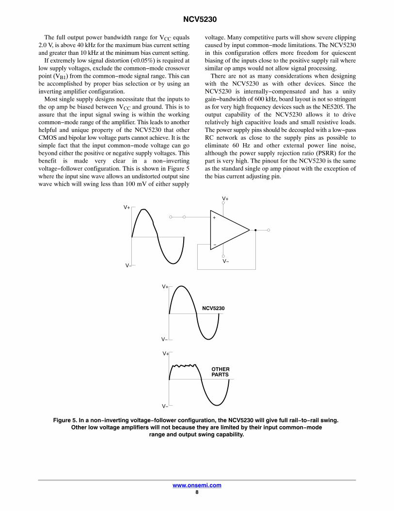
The full output power bandwidth range for VCC equals2.0 V, is above 40 kHz for the maximum bias current settingand greater than 10 kHz at the minimum bias current setting.
If extremely low signal distortion (<0.05%) is required atlow supply voltages, exclude the common−mode crossoverpoint (VB1) from the common−mode signal range. This canbe accomplished by proper bias selection or by using aninverting amplifier configuration.
Most single supply designs necessitate that the inputs tothe op amp be biased between VCC and ground. This is toassure that the input signal swing is within the workingcommon−mode range of the amplifier. This leads to anotherhelpful and unique property of the NCV5230 that otherCMOS and bipolar low voltage parts cannot achieve. It is thesimple fact that the input common−mode voltage can gobeyond either the positive or negative supply voltages. Thisbenefit is made very clear in a non−invertingvoltage−follower configuration. This is shown in Figure 5where the input sine wave allows an undistorted output sinewave which will swing less than 100 mV of either supply
voltage. Many competitive parts will show severe clippingcaused by input common−mode limitations. The NCV5230in this configuration offers more freedom for quiescentbiasing of the inputs close to the positive supply rail wheresimilar op amps would not allow signal processing.
There are not as many considerations when designingwith the NCV5230 as with other devices. Since theNCV5230 is internally−compensated and has a unitygain−bandwidth of 600 kHz, board layout is not so stringentas for very high frequency devices such as the NE5205. Theoutput capability of the NCV5230 allows it to driverelatively high capacitive loads and small resistive loads.The power supply pins should be decoupled with a low−passRC network as close to the supply pins as possible toeliminate 60 Hz and other external power line noise,although the power supply rejection ratio (PSRR) for thepart is very high. The pinout for the NCV5230 is the sameas the standard single op amp pinout with the exception ofthe bias current adjusting pin.
V+
V−
+
−
NCV5230
OTHERPARTS
V+
V−
V+
V−
V+
V−
Figure 5. In a non−inverting voltage−follower configuration, the NCV5230 will give full rail−to−rail swing. Other low voltage amplifiers will not because they are limited by their input common−mode
range and output swing capability.

NCV5230
www.onsemi.com9
REMOTE TRANSDUCER WITH CURRENTTRANSMISSION
There are many ways to transmit information along twowires, but current transmission is the most beneficial whenthe sensing of remote signals is the aim. It is furtherenhanced in the form of 4.0 to 20 mA information which isused in many control−type systems. This method oftransmission provides immunity from line voltage drops,large load resistance variations, and voltage noise pickup.The zero reference of 4mA not only can show if there is abreak in the line when no current is flowing, but also canpower the transducer at the remote location. Usually thetransducer itself is not equipped to provide for the currenttransmission. The unique features of the NCV5230 canprovide high output current capability coupled with lowpower consumption. It can be remotely connected to thetransducer to create a current loop with minimal externalcomponents. The circuits for this are shown in Figures 6and 7. Here, the part is configured as a voltage−to−current,or transconductance amplifier. This is a novel circuit thattakes advantage of the NCV5230’s large open−loop gain. InAC applications, the load current will decrease as theopen−loop gain rolls off in magnitude. The low offsetvoltage and current sinking capabilities of the NCV5230must also be considered in this application.
The NCV5230 circuit shown in Figure 6 is a pseudotransistor configuration. The inverting input is equivalent tothe “base,” the point where VEE and the non−inverting inputmeet is the “emitter,” and the connection after the outputdiode meets the VCC pin is the collector. The output diodeis essential to keep the output from saturating in thisconfiguration. From here it can be seen that the base andemitter form a voltage−follower and the voltage present atRC must equal the input voltage present at the invertinginput. Also, the emitter and collector form acurrent−follower and the current flowing through RC isequivalent to the current through RL and the amplifier. Thissets up the current loop. Therefore, the following equationcan be formulated for the working current transmission line.The load current is:
IL �VINRC
(eq. 2)
and proportional to the input voltage for a set RC. Also, thecurrent is constant no matter what load resistance is usedwhile within the operating bandwidth range of the op amp.When the NCV5230’s supply voltage falls past a certainpoint, the current cannot remain constant. This is the“voltage compliance” and is very good for this applicationbecause of the near rail output voltage. The equation thatdetermines the voltage compliance as well as the largestpossible load resistor for the NCV5230 is as follows:
RLmax ��Vremote supply � VCC min� VIN max�
IL(eq. 3)
Where VCC min is the worst−case power supply voltage(approximately 1.8 V) that will still keep the partoperational. As an example, when using a 15 V remotepower supply, a current sensing resistor of 1.0 �, and aninput voltage (VIN) of 20 mV, the output current (IL) is20 mA. Furthermore, a load resistance of zero toapproximately 650 � can be inserted in the loop without anychange in current when the bias current−control pin is tiedto the negative supply pin. The voltage drop across the loadand line resistance will not affect the NCV5230 because itwill operate down to 1.8 V. With a 15 V remote supply, thevoltage available at the amplifier is still enough to power itwith the maximum 20 mA output into the 650 � load.
Figure 6. The NCV5230 as a Remote TransducerTransconductance Amp with 4.0 − 20 mA Current
Transmission Output Capability
TRANSDUCER
VREMOTEPOWERSUPPLY
NCV5230
VCC
VEE
VIN
IOUT3
24
5
6
7 +
−
RC
RL
+
−
NOTES:1. IOUT = VIN/RC
2. RL MAX ≈VREMOTE � 1.8V � VINMAX
IOUT
For RC = 1.0 �IOUT
4mAVIN
4mV20mA 20mV
Figure 7. The Same Type of Circuit as Figure 6, butfor Sourcing Current to the Load
VCC
NCV5230
3
24
5
6
7+
−VEE + IOUT
+
−
VIN
RC
RL
VCC
+
−

NCV5230
www.onsemi.com10
What this means is that several instruments, such as a chartrecorder, a meter, or a controller, as well as a long cable, canbe connected in series on the loop and still obtain accuratereadings if the total resistance does not exceed 650 �.Furthermore, any variation of resistance in this range willnot change the output current.
Any voltage output type transducer can be used, but onethat does not need external DC voltage or current excitationto limit the maximum possible load resistance is preferable.Even this problem can be surmounted if the supply powerneeded by the transducer is compatible with the NCV5230.The power goes up the line to the transducer and amplifierwhile the transducer signal is sent back via the current outputof the NCV5230 transconductance configuration.
The voltage range on the input can be changed fortransducers that produce a large output by simply increasingthe current sense resistor to get the corresponding 4.0 to20 mA output current. If a very long line is used whichcauses high line resistance, a current repeater could beinserted into the line. The same configuration of Figure 7 canbe used with exception of a resistor across the input and line
ground to convert the current back to voltage. Again, thecurrent sensing resistor will set up the transconductance andthe part will receive power from the line.
TEMPERATURE TRANSDUCERA variation on the previous circuit makes use of the supply
current control pin. The voltage present at this pin isproportional to absolute temperature (PTAT) because it isproduced by the amplifier bias current through an internalresistor divider in a PTAT cell. If the control pin is connectedto the input pin, the NCV5230 itself can be used as atemperature transducer. If the center tap of a resistive pot isconnected to the control pin with one side to ground and theother to the inverting input, the voltage can be changed togive different temperature versus output current conditions(Figure 8). For additional control, the output current is stillproportional to the input voltage differential divided by thecurrent sense resistor.
When using the NCV5230 as a temperature transducer,the thermal considerations in the previous section must bekept in mind.
VREMOTEPOWERSUPPLY
NCV5230
VCC
VEE
IOUT3
2
4
5
6
7 +
−
RC
RL
+
−
NOTES:1. IOUT = VIN/RC
2. RL MAX ≈VREMOTE � 1.8V � VINMAX
IOUTFor RC = 1�IOUT
4mA20mA
VIN
4mV20mV
200
Figure 8. NCV5230 remote temperature transducer utilizing 4.0 − 20 mA current transmission. This applicationshows the use of the accessibility of the PTAT cell in the device to make the part, itself, a transducer.
10�

NCV5230
www.onsemi.com11
HALF−WAVE RECTIFIER WITHRAIL−TO−GROUND OUTPUT SWING
Since the NCV5230 input common−mode range includesboth positive and negative supply rails and the output canalso swing to either supply, achieving half−wave rectifierfunctions in either direction becomes a simple task. All thatis needed are two external resistors; there is no need fordiodes or matched resistors. Moreover, it can have eitherpositive− or negative−going outputs, depending on the waythe bias is arranged. In Figure 9, the circuit is biased toground, while circuit (Figure 10) is biased to the positivesupply. This rather unusual biasing does not cause anyproblems with the NCV5230 because of the unique internalsaturation detectors incorporated into the part to keep thePNP and NPN output transistors out of “hard” saturation. Itis therefore relatively quick to recover from a saturatedoutput condition. Furthermore, the device does not haveparasitic current draw when the output is biased to either rail.
This makes it possible to bias the NCV5230 into“saturation” and obtain half−wave rectification with goodrecovery. The simplicity of biasing and the rail−to−groundhalf−sine wave swing are unique to this device. The circuitgain can be changed by the standard op amp gain equationsfor an inverting configuration.
It can be seen in these configurations that the op ampcannot respond to one−half of the incoming waveform. Itcannot respond because the waveform forces the amplifierto swing the output beyond either ground or the positivesupply rail, depending on the biasing, and, also, the outputcannot disengage during this half cycle. During the otherhalf cycle, however, the amplifier achieves a half−wave thatcan have a peak equal to the total supply voltage. Thephotographs in Figure 11 show the effect of the differentbiasing schemes, as well as the wide bandwidth (it worksover the full audio range), that the NCV5230 can achieve inthis configuration.
VCC
Figure 9. Rail−to−Ground Output Swing Referenced to Ground
Figure 10. Negative−Going Output Referenced to VCC
VIN
VCC
2
34
5
67−
+
Ot
VCCVOUT
t
VCC
3
24
5
67
VIN
VOUT
VCC
−
+
Half−Wave Rectifier With Positive−Going Output Swings
10�
10�
10�
10�

NCV5230
www.onsemi.com12
500 mV/Div 200�S /DivBiased to Ground
500 mV/Div 20 �S/DivBiased to Ground
500 mV/Div 20 �S/DivBiased to Positive Rail
Figure 11. Performance Waveforms for the Circuits in Figures 9 and 10. Good response is shown at 1.0 and 10 kHz for both circuits under full swing with a 2.0 V supply.

NCV5230
www.onsemi.com13
By adding another NCV5230 in an inverting summerconfiguration at the output of the half−wave rectifier, afull−wave can be realized. The values for the input andfeedback resistors must be chosen so that each peak willhave equal amplitudes. A table for calculating values isincluded in Figure 12. The summing network combines theinput signal at the half−wave and adds it to double thehalf−wave’s output, resulting in the full−wave. The output
waveform can be referenced to the supply or ground,depending on the half−wave configuration. Again, nodiodes are needed to achieve the rectification.
This circuit could be used in conjunction with the remotetransducer to convert a received AC output signal into a DClevel at the full−wave output for meters or chart recordersthat need DC levels.
HALF-WAVE
a
b
+VIN
−VIN
a
b
+VIN
−VIN
a b+VIN
+VBFULL-WAVE
2a
−2VIN
0
VEE
VEE
VCC
+VB
R1
3
2 45
6
7
R2
R3 R5
R4 2
34
5
6
7
+
−
+
−A1
A2
INPUT
HALF-WAVEOUTPUT
FULL-WAVEOUTPUT
500mV 500mV
500mV
520�s
NOTES:R2 = 2 R1R4 = R5 = R3+VB will vary output reference.For single supply operation VEEcan be grounded on A2.
Figure 12. Adding an Inverting Summer to the Input and Output of the Half−Wave will Result in Full−Wave

NCV5230
www.onsemi.com14
CONCLUSIONThe NCV5230 is a versatile op amp in its own right. The
part was designed to give low voltage and low poweroperation without the limitations of previously availableamplifiers that had a multitude of problems. The previousapplication examples are unique to this amplifier and savethe user money by excluding various passive componentsthat would have been needed if not for the NCV5230’sspecial input and output stages.
The NCV5230 has a combination of novel specificationswhich allows the designer to implement it easily intoexisting low−supply voltage designs and to enhance theirperformance. It also offers the engineer the freedom toachieve greater amplifier system design goals. The low inputreferenced noise voltage eases the restrictions on designswhere S/N ratios are important. The wide full−powerbandwidth and output load handling capability allow it to fitinto portable audio applications. The truly ample open−loopgain and low power consumption easily lend themselves tothe requirements of remote transducer applications. Thelow, untrimmed typical offset voltage and low offsetcurrents help to reduce errors in signal processing designs.The amplifier is well isolated from changes on the supplylines by its typical power supply rejection ratio of 105 dB.
REFERENCES1. Johan H. Huijsing, Multi−stage Amplifier with
Capacitive Nesting for Frequency Compensation,U.S. Patent Application Serial No. 602.234, filedApril 19, 1984.
2. Bob Blauschild, Differential Amplifier withRail−to−Rail Capability, U.S. Patent ApplicationSerial No. 525.181, filed August 23, 1983.
3. Operational Amplifiers − Characteristics andApplications, Robert G. Irvine, Prentice−Hall, Inc.,Englewood Cliffs, NJ 07632, 1981.
4. Transducer Interface Handbook − A Guide toAnalog Signal Conditioning, Edited by Daniel H.Sheingold, Analog Devices, Inc., Norwood, MA02062, 1981.

NCV5230
www.onsemi.com15
SOIC−8D SUFFIXCASE 751
A = Assembly LocationL = Wafer LotY = YearW = Work Week� = Pb−Free Package
MARKING DIAGRAMS
S5230ALYWE
�1
8
ORDERING INFORMATION
Device Description Temperature Range Shipping†
NCV5230DR2G8−Pin Plastic Small Outline (SO−8) Package
(Pb−Free) −40°C to +125°C 2500 / Tape & Reel
†For information on tape and reel specifications, including part orientation and tape sizes, please refer to our Tape and Reel PackagingSpecifications Brochure, BRD8011/D.

PDIP−8CASE 626−05
ISSUE PDATE 22 APR 2015
SCALE 1:1
1 4
58
b2NOTE 8
D
b
L
A1
A
eB
XXXXXXXXXAWL
YYWWG
E
GENERICMARKING DIAGRAM*
XXXX = Specific Device CodeA = Assembly LocationWL = Wafer LotYY = YearWW = Work WeekG = Pb−Free Package
*This information is generic. Please refer todevice data sheet for actual part marking.Pb−Free indicator, “G” or microdot “ �”,may or may not be present.
A
TOP VIEW
C
SEATINGPLANE
0.010 C ASIDE VIEW
END VIEW
END VIEW
WITH LEADS CONSTRAINED
DIM MIN MAXINCHES
A −−−− 0.210A1 0.015 −−−−
b 0.014 0.022
C 0.008 0.014D 0.355 0.400D1 0.005 −−−−
e 0.100 BSC
E 0.300 0.325
M −−−− 10
−−− 5.330.38 −−−
0.35 0.56
0.20 0.369.02 10.160.13 −−−
2.54 BSC
7.62 8.26
−−− 10
MIN MAXMILLIMETERS
NOTES:1. DIMENSIONING AND TOLERANCING PER ASME Y14.5M, 1994.2. CONTROLLING DIMENSION: INCHES.3. DIMENSIONS A, A1 AND L ARE MEASURED WITH THE PACK-
AGE SEATED IN JEDEC SEATING PLANE GAUGE GS−3.4. DIMENSIONS D, D1 AND E1 DO NOT INCLUDE MOLD FLASH
OR PROTRUSIONS. MOLD FLASH OR PROTRUSIONS ARENOT TO EXCEED 0.10 INCH.
5. DIMENSION E IS MEASURED AT A POINT 0.015 BELOW DATUMPLANE H WITH THE LEADS CONSTRAINED PERPENDICULARTO DATUM C.
6. DIMENSION eB IS MEASURED AT THE LEAD TIPS WITH THELEADS UNCONSTRAINED.
7. DATUM PLANE H IS COINCIDENT WITH THE BOTTOM OF THELEADS, WHERE THE LEADS EXIT THE BODY.
8. PACKAGE CONTOUR IS OPTIONAL (ROUNDED OR SQUARECORNERS).
E1 0.240 0.280 6.10 7.11
b2
eB −−−− 0.430 −−− 10.92
0.060 TYP 1.52 TYP
E1
M
8X
c
D1
B
A2 0.115 0.195 2.92 4.95
L 0.115 0.150 2.92 3.81°°
H
NOTE 5
e
e/2A2
NOTE 3
M B M NOTE 6
M
STYLE 1:PIN 1. AC IN
2. DC + IN3. DC − IN4. AC IN5. GROUND6. OUTPUT7. AUXILIARY8. VCC
MECHANICAL CASE OUTLINE
PACKAGE DIMENSIONS
ON Semiconductor and are trademarks of Semiconductor Components Industries, LLC dba ON Semiconductor or its subsidiaries in the United States and/or other countries.ON Semiconductor reserves the right to make changes without further notice to any products herein. ON Semiconductor makes no warranty, representation or guarantee regardingthe suitability of its products for any particular purpose, nor does ON Semiconductor assume any liability arising out of the application or use of any product or circuit, and specificallydisclaims any and all liability, including without limitation special, consequential or incidental damages. ON Semiconductor does not convey any license under its patent rights nor therights of others.
98ASB42420BDOCUMENT NUMBER:
DESCRIPTION:
Electronic versions are uncontrolled except when accessed directly from the Document Repository.Printed versions are uncontrolled except when stamped “CONTROLLED COPY” in red.
PAGE 1 OF 1PDIP−8
© Semiconductor Components Industries, LLC, 2019 www.onsemi.com

SOIC−8 NBCASE 751−07
ISSUE AKDATE 16 FEB 2011
SEATINGPLANE
14
58
N
J
X 45�
K
NOTES:1. DIMENSIONING AND TOLERANCING PER
ANSI Y14.5M, 1982.2. CONTROLLING DIMENSION: MILLIMETER.3. DIMENSION A AND B DO NOT INCLUDE
MOLD PROTRUSION.4. MAXIMUM MOLD PROTRUSION 0.15 (0.006)
PER SIDE.5. DIMENSION D DOES NOT INCLUDE DAMBAR
PROTRUSION. ALLOWABLE DAMBARPROTRUSION SHALL BE 0.127 (0.005) TOTALIN EXCESS OF THE D DIMENSION ATMAXIMUM MATERIAL CONDITION.
6. 751−01 THRU 751−06 ARE OBSOLETE. NEWSTANDARD IS 751−07.
A
B S
DH
C
0.10 (0.004)
SCALE 1:1
STYLES ON PAGE 2
DIMA
MIN MAX MIN MAXINCHES
4.80 5.00 0.189 0.197
MILLIMETERS
B 3.80 4.00 0.150 0.157C 1.35 1.75 0.053 0.069D 0.33 0.51 0.013 0.020G 1.27 BSC 0.050 BSCH 0.10 0.25 0.004 0.010J 0.19 0.25 0.007 0.010K 0.40 1.27 0.016 0.050M 0 8 0 8 N 0.25 0.50 0.010 0.020S 5.80 6.20 0.228 0.244
−X−
−Y−
G
MYM0.25 (0.010)
−Z−
YM0.25 (0.010) Z S X S
M� � � �
XXXXX = Specific Device CodeA = Assembly LocationL = Wafer LotY = YearW = Work Week� = Pb−Free Package
GENERICMARKING DIAGRAM*
1
8
XXXXXALYWX
1
8
IC Discrete
XXXXXXAYWW
�1
8
1.520.060
7.00.275
0.60.024
1.2700.050
4.00.155
� mminches
�SCALE 6:1
*For additional information on our Pb−Free strategy and solderingdetails, please download the ON Semiconductor Soldering andMounting Techniques Reference Manual, SOLDERRM/D.
SOLDERING FOOTPRINT*
Discrete
XXXXXXAYWW
1
8
(Pb−Free)
XXXXXALYWX
�1
8
IC(Pb−Free)
XXXXXX = Specific Device CodeA = Assembly LocationY = YearWW = Work Week� = Pb−Free Package
*This information is generic. Please refer todevice data sheet for actual part marking.Pb−Free indicator, “G” or microdot “�”, mayor may not be present. Some products maynot follow the Generic Marking.
MECHANICAL CASE OUTLINE
PACKAGE DIMENSIONS
ON Semiconductor and are trademarks of Semiconductor Components Industries, LLC dba ON Semiconductor or its subsidiaries in the United States and/or other countries.ON Semiconductor reserves the right to make changes without further notice to any products herein. ON Semiconductor makes no warranty, representation or guarantee regardingthe suitability of its products for any particular purpose, nor does ON Semiconductor assume any liability arising out of the application or use of any product or circuit, and specificallydisclaims any and all liability, including without limitation special, consequential or incidental damages. ON Semiconductor does not convey any license under its patent rights nor therights of others.
98ASB42564BDOCUMENT NUMBER:
DESCRIPTION:
Electronic versions are uncontrolled except when accessed directly from the Document Repository.Printed versions are uncontrolled except when stamped “CONTROLLED COPY” in red.
PAGE 1 OF 2SOIC−8 NB
© Semiconductor Components Industries, LLC, 2019 www.onsemi.com

SOIC−8 NBCASE 751−07
ISSUE AKDATE 16 FEB 2011
STYLE 4:PIN 1. ANODE
2. ANODE3. ANODE4. ANODE5. ANODE6. ANODE7. ANODE8. COMMON CATHODE
STYLE 1:PIN 1. EMITTER
2. COLLECTOR3. COLLECTOR4. EMITTER5. EMITTER6. BASE7. BASE8. EMITTER
STYLE 2:PIN 1. COLLECTOR, DIE, #1
2. COLLECTOR, #13. COLLECTOR, #24. COLLECTOR, #25. BASE, #26. EMITTER, #27. BASE, #18. EMITTER, #1
STYLE 3:PIN 1. DRAIN, DIE #1
2. DRAIN, #13. DRAIN, #24. DRAIN, #25. GATE, #26. SOURCE, #27. GATE, #18. SOURCE, #1
STYLE 6:PIN 1. SOURCE
2. DRAIN3. DRAIN4. SOURCE5. SOURCE6. GATE7. GATE8. SOURCE
STYLE 5:PIN 1. DRAIN
2. DRAIN3. DRAIN4. DRAIN5. GATE6. GATE7. SOURCE8. SOURCE
STYLE 7:PIN 1. INPUT
2. EXTERNAL BYPASS3. THIRD STAGE SOURCE4. GROUND5. DRAIN6. GATE 37. SECOND STAGE Vd8. FIRST STAGE Vd
STYLE 8:PIN 1. COLLECTOR, DIE #1
2. BASE, #13. BASE, #24. COLLECTOR, #25. COLLECTOR, #26. EMITTER, #27. EMITTER, #18. COLLECTOR, #1
STYLE 9:PIN 1. EMITTER, COMMON
2. COLLECTOR, DIE #13. COLLECTOR, DIE #24. EMITTER, COMMON5. EMITTER, COMMON6. BASE, DIE #27. BASE, DIE #18. EMITTER, COMMON
STYLE 10:PIN 1. GROUND
2. BIAS 13. OUTPUT4. GROUND5. GROUND6. BIAS 27. INPUT8. GROUND
STYLE 11:PIN 1. SOURCE 1
2. GATE 13. SOURCE 24. GATE 25. DRAIN 26. DRAIN 27. DRAIN 18. DRAIN 1
STYLE 12:PIN 1. SOURCE
2. SOURCE3. SOURCE4. GATE5. DRAIN6. DRAIN7. DRAIN8. DRAIN
STYLE 14:PIN 1. N−SOURCE
2. N−GATE3. P−SOURCE4. P−GATE5. P−DRAIN6. P−DRAIN7. N−DRAIN8. N−DRAIN
STYLE 13:PIN 1. N.C.
2. SOURCE3. SOURCE4. GATE5. DRAIN6. DRAIN7. DRAIN8. DRAIN
STYLE 15:PIN 1. ANODE 1
2. ANODE 13. ANODE 14. ANODE 15. CATHODE, COMMON6. CATHODE, COMMON7. CATHODE, COMMON8. CATHODE, COMMON
STYLE 16:PIN 1. EMITTER, DIE #1
2. BASE, DIE #13. EMITTER, DIE #24. BASE, DIE #25. COLLECTOR, DIE #26. COLLECTOR, DIE #27. COLLECTOR, DIE #18. COLLECTOR, DIE #1
STYLE 17:PIN 1. VCC
2. V2OUT3. V1OUT4. TXE5. RXE6. VEE7. GND8. ACC
STYLE 18:PIN 1. ANODE
2. ANODE3. SOURCE4. GATE5. DRAIN6. DRAIN7. CATHODE8. CATHODE
STYLE 19:PIN 1. SOURCE 1
2. GATE 13. SOURCE 24. GATE 25. DRAIN 26. MIRROR 27. DRAIN 18. MIRROR 1
STYLE 20:PIN 1. SOURCE (N)
2. GATE (N)3. SOURCE (P)4. GATE (P)5. DRAIN6. DRAIN7. DRAIN8. DRAIN
STYLE 21:PIN 1. CATHODE 1
2. CATHODE 23. CATHODE 34. CATHODE 45. CATHODE 56. COMMON ANODE7. COMMON ANODE8. CATHODE 6
STYLE 22:PIN 1. I/O LINE 1
2. COMMON CATHODE/VCC3. COMMON CATHODE/VCC4. I/O LINE 35. COMMON ANODE/GND6. I/O LINE 47. I/O LINE 58. COMMON ANODE/GND
STYLE 23:PIN 1. LINE 1 IN
2. COMMON ANODE/GND3. COMMON ANODE/GND4. LINE 2 IN5. LINE 2 OUT6. COMMON ANODE/GND7. COMMON ANODE/GND8. LINE 1 OUT
STYLE 24:PIN 1. BASE
2. EMITTER3. COLLECTOR/ANODE4. COLLECTOR/ANODE5. CATHODE6. CATHODE7. COLLECTOR/ANODE8. COLLECTOR/ANODE
STYLE 25:PIN 1. VIN
2. N/C3. REXT4. GND5. IOUT6. IOUT7. IOUT8. IOUT
STYLE 26:PIN 1. GND
2. dv/dt3. ENABLE4. ILIMIT5. SOURCE6. SOURCE7. SOURCE8. VCC
STYLE 27:PIN 1. ILIMIT
2. OVLO3. UVLO4. INPUT+5. SOURCE6. SOURCE7. SOURCE8. DRAIN
STYLE 28:PIN 1. SW_TO_GND
2. DASIC_OFF3. DASIC_SW_DET4. GND5. V_MON6. VBULK7. VBULK8. VIN
STYLE 29:PIN 1. BASE, DIE #1
2. EMITTER, #13. BASE, #24. EMITTER, #25. COLLECTOR, #26. COLLECTOR, #27. COLLECTOR, #18. COLLECTOR, #1
STYLE 30:PIN 1. DRAIN 1
2. DRAIN 13. GATE 24. SOURCE 25. SOURCE 1/DRAIN 26. SOURCE 1/DRAIN 27. SOURCE 1/DRAIN 28. GATE 1
ON Semiconductor and are trademarks of Semiconductor Components Industries, LLC dba ON Semiconductor or its subsidiaries in the United States and/or other countries.ON Semiconductor reserves the right to make changes without further notice to any products herein. ON Semiconductor makes no warranty, representation or guarantee regardingthe suitability of its products for any particular purpose, nor does ON Semiconductor assume any liability arising out of the application or use of any product or circuit, and specificallydisclaims any and all liability, including without limitation special, consequential or incidental damages. ON Semiconductor does not convey any license under its patent rights nor therights of others.
98ASB42564BDOCUMENT NUMBER:
DESCRIPTION:
Electronic versions are uncontrolled except when accessed directly from the Document Repository.Printed versions are uncontrolled except when stamped “CONTROLLED COPY” in red.
PAGE 2 OF 2SOIC−8 NB
© Semiconductor Components Industries, LLC, 2019 www.onsemi.com

onsemi, , and other names, marks, and brands are registered and/or common law trademarks of Semiconductor Components Industries, LLC dba “onsemi” or its affiliatesand/or subsidiaries in the United States and/or other countries. onsemi owns the rights to a number of patents, trademarks, copyrights, trade secrets, and other intellectual property.A listing of onsemi’s product/patent coverage may be accessed at www.onsemi.com/site/pdf/Patent−Marking.pdf. onsemi reserves the right to make changes at any time to anyproducts or information herein, without notice. The information herein is provided “as−is” and onsemi makes no warranty, representation or guarantee regarding the accuracy of theinformation, product features, availability, functionality, or suitability of its products for any particular purpose, nor does onsemi assume any liability arising out of the application or useof any product or circuit, and specifically disclaims any and all liability, including without limitation special, consequential or incidental damages. Buyer is responsible for its productsand applications using onsemi products, including compliance with all laws, regulations and safety requirements or standards, regardless of any support or applications informationprovided by onsemi. “Typical” parameters which may be provided in onsemi data sheets and/or specifications can and do vary in different applications and actual performance mayvary over time. All operating parameters, including “Typicals” must be validated for each customer application by customer’s technical experts. onsemi does not convey any licenseunder any of its intellectual property rights nor the rights of others. onsemi products are not designed, intended, or authorized for use as a critical component in life support systemsor any FDA Class 3 medical devices or medical devices with a same or similar classification in a foreign jurisdiction or any devices intended for implantation in the human body. ShouldBuyer purchase or use onsemi products for any such unintended or unauthorized application, Buyer shall indemnify and hold onsemi and its officers, employees, subsidiaries, affiliates,and distributors harmless against all claims, costs, damages, and expenses, and reasonable attorney fees arising out of, directly or indirectly, any claim of personal injury or deathassociated with such unintended or unauthorized use, even if such claim alleges that onsemi was negligent regarding the design or manufacture of the part. onsemi is an EqualOpportunity/Affirmative Action Employer. This literature is subject to all applicable copyright laws and is not for resale in any manner.
PUBLICATION ORDERING INFORMATIONTECHNICAL SUPPORTNorth American Technical Support:Voice Mail: 1 800−282−9855 Toll Free USA/CanadaPhone: 011 421 33 790 2910
LITERATURE FULFILLMENT:Email Requests to: [email protected]
onsemi Website: www.onsemi.com
Europe, Middle East and Africa Technical Support:Phone: 00421 33 790 2910For additional information, please contact your local Sales Representative
◊