Operational Amplifier (Opamp)
13
PSoC® Creator™ Component Data Sheet Cypress Semiconductor Corporation • 198 Champion Court • San Jose, CA 95134-1709 • 408-943-2600 Document Number: 001-60897 Rev. *B Revised August 1, 2016 PRELIMINARY Features Follower or Opamp configuration Unity gain bandwidth > 3.0 MHz Input offset voltage 2.0 mV max Rail-to-rail inputs and output Output direct low resistance connection to pin 25 mA output current Programmable power and bandwidth Internal connection for follower (saves pin) General Description The Opamp component provides a low voltage, low power operational amplifier and may be internally connected as a voltage follower. The inputs and output may be connected to internal routing nodes, directly to pins, or a combination of internal and external signals. The Opamp is suitable for interfacing with high impedance sensors, buffering the output of voltage DACs, driving up to 25 mA; and constructing active filters in any standard topology. Input/Output Connections This section describes the various input and output connections for the Opamp. An asterisk (*) in the list of I/Os indicates that the I/O may be hidden on the symbol under the conditions listed in the description of that I/O. Non-Inverting – Analog When the Opamp is configured as a follower, this I/O is the voltage input. If the Opamp is configured as an Opamp, this I/O acts as the standard Opamp non-inverting input. Inverting – Analog * When the Opamp component is configured for Opamp mode, this I/O is the normal inverting input. When the Opamp is configured for Follower mode, this I/O is hard-connected to the output and the I/O is unavailable. Operational Amplifier (Opamp) 1.50
-
Upload
khangminh22 -
Category
Documents
-
view
0 -
download
0
Transcript of Operational Amplifier (Opamp)
PSoC® Creator™ Component Data Sheet
Cypress Semiconductor Corporation • 198 Champion Court • San Jose, CA 95134-1709 • 408-943-2600
Document Number: 001-60897 Rev. *B Revised August 1, 2016
PRELIMINARY
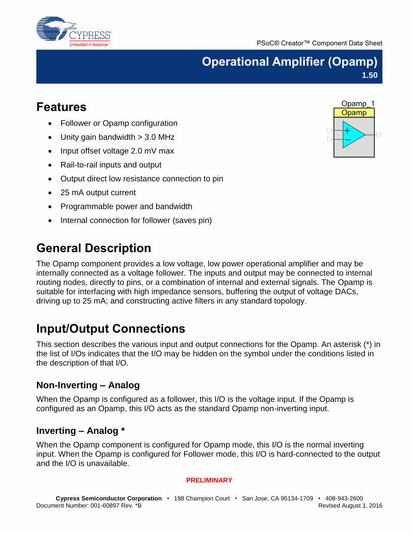
Features
Follower or Opamp configuration
Unity gain bandwidth > 3.0 MHz
Input offset voltage 2.0 mV max
Rail-to-rail inputs and output
Output direct low resistance connection to pin
25 mA output current
Programmable power and bandwidth
Internal connection for follower (saves pin)
General Description
The Opamp component provides a low voltage, low power operational amplifier and may be internally connected as a voltage follower. The inputs and output may be connected to internal routing nodes, directly to pins, or a combination of internal and external signals. The Opamp is suitable for interfacing with high impedance sensors, buffering the output of voltage DACs, driving up to 25 mA; and constructing active filters in any standard topology.
Input/Output Connections
This section describes the various input and output connections for the Opamp. An asterisk (*) in the list of I/Os indicates that the I/O may be hidden on the symbol under the conditions listed in the description of that I/O.
Non-Inverting – Analog
When the Opamp is configured as a follower, this I/O is the voltage input. If the Opamp is configured as an Opamp, this I/O acts as the standard Opamp non-inverting input.
Inverting – Analog *
When the Opamp component is configured for Opamp mode, this I/O is the normal inverting input. When the Opamp is configured for Follower mode, this I/O is hard-connected to the output and the I/O is unavailable.
Operational Amplifier (Opamp) 1.50
Operational Amplifier (Opamp) PSoC® Creator™ Component Data Sheet
Page 2 of 13 Document Number: 001-60897 Rev. *B
PRELIMINARY
Vout – Analog
The output is directly connected to a pin. It is capable of driving 25 mA and can be connected to internal loads using the analog routing fabric. When used for internal routing, the output remains connected to the pin.
Schematic Macro Information
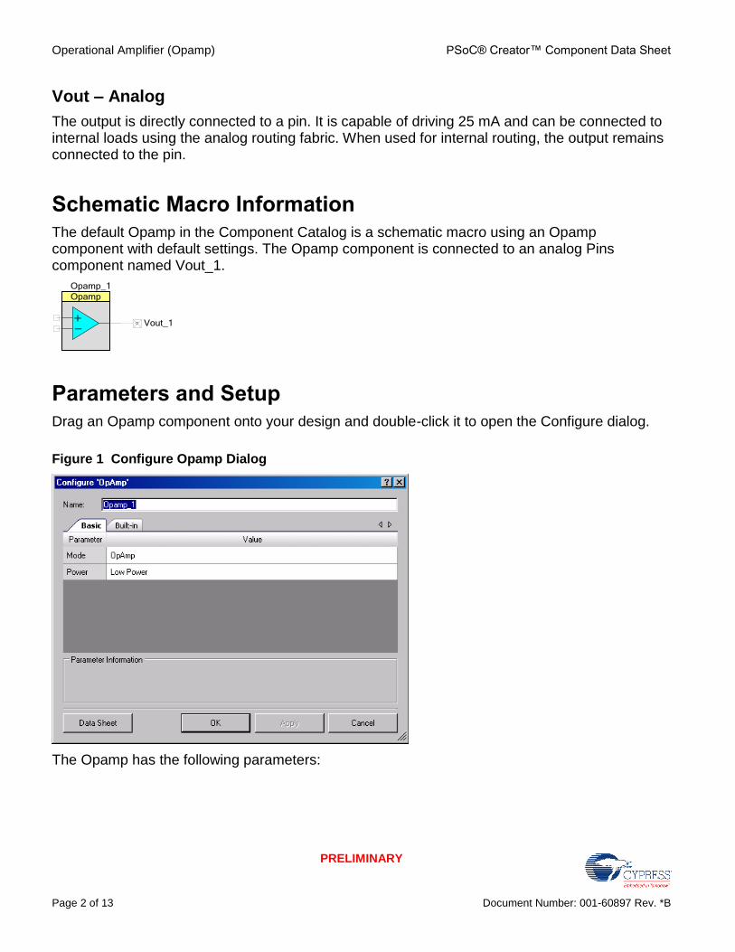
The default Opamp in the Component Catalog is a schematic macro using an Opamp component with default settings. The Opamp component is connected to an analog Pins component named Vout_1.
Parameters and Setup
Drag an Opamp component onto your design and double-click it to open the Configure dialog.
Figure 1 Configure Opamp Dialog
The Opamp has the following parameters:

PSoC® Creator™ Component Data Sheet Operational Amplifier (Opamp)
Document Number: 001-60897 Rev. *B Page 3 of 13
PRELIMINARY
Mode
This parameter allows you to select between two configurations: "Opamp" and "Follower". In Opamp mode, all three terminals are available for connection. In Follower mode, the inverting input is internally connected to the output to create a voltage follower. Opamp is the default configuration.
Figure 2 Configuration Options
Power
The Opamp works over a wide range of operating currents. Higher operating current increases Opamp bandwidth. The Power parameter allows you to select the power level:
In High and Medium power modes, the output is a class AB stage, enabling direct drive of substantial output currents.
In Low power mode, the output is a class A stage with limited current drive.
In Slow mode, the output is a class A stage.
The Slow mode is used for low-power transimpedance amplifiers (TIAs). The Slow mode has the same drive capability as low power, but includes additional compensation for circuit topologies with higher than normal input capacitance as is often seen in photo sensors and other current-output sensors of various types.
Wider bandwidth TIAs can be implemented using the medium or high power settings. In this case, exercise the usual care in dealing with compensation for capacitively loaded sources.
Placement
Each Opamp is directly connected to specific GPIOs.
Non-inverting input Inverting input Output
opamp_0 P0[2] P0[3] P0[1]
opamp_1 P3[5] P3[4] P3[6]
opamp_2 P0[4] P0[5] P0[0]
opamp_3 P3[3] P3[2] P3[7]
Operational Amplifier (Opamp) PSoC® Creator™ Component Data Sheet
Page 4 of 13 Document Number: 001-60897 Rev. *B
PRELIMINARY
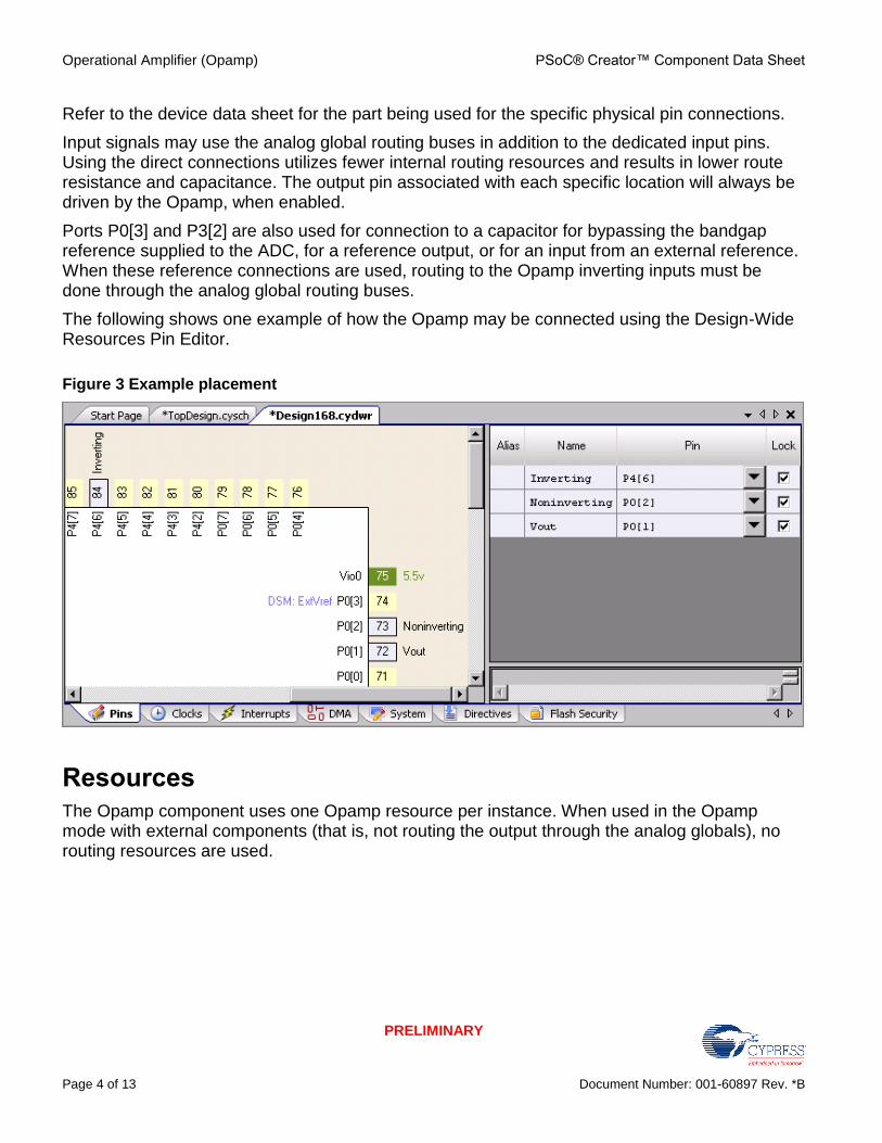
Refer to the device data sheet for the part being used for the specific physical pin connections.
Input signals may use the analog global routing buses in addition to the dedicated input pins. Using the direct connections utilizes fewer internal routing resources and results in lower route resistance and capacitance. The output pin associated with each specific location will always be driven by the Opamp, when enabled.
Ports P0[3] and P3[2] are also used for connection to a capacitor for bypassing the bandgap reference supplied to the ADC, for a reference output, or for an input from an external reference. When these reference connections are used, routing to the Opamp inverting inputs must be done through the analog global routing buses.
The following shows one example of how the Opamp may be connected using the Design-Wide Resources Pin Editor.
Figure 3 Example placement
Resources
The Opamp component uses one Opamp resource per instance. When used in the Opamp mode with external components (that is, not routing the output through the analog globals), no routing resources are used.
PSoC® Creator™ Component Data Sheet Operational Amplifier (Opamp)
Document Number: 001-60897 Rev. *B Page 5 of 13
PRELIMINARY
Application Programming Interface
Application Programming Interface (API) routines allow you to configure the component using software. The following table lists and describes the interface to each function. The subsequent sections cover each function in more detail.
By default, PSoC Creator assigns the instance name "Opamp_1" to the first instance of a component in a given design. You can rename it to any unique value that follows the syntactic rules for identifiers. The instance name becomes the prefix of every global function name, variable, and constant symbol. For readability, the instance name used in the following table is "Opamp".
Function Description
void Opamp_Init(void) Initializes or restores default Opamp configuration.
void Opamp_Enable(void) Enables the Opamp.
void Opamp_Start(void) Turns on the Opamp and sets the power level to the value chosen during the parameter selection.
void Opamp_Stop(void) Disable Opamp (power down)
void Opamp_SetPower(uint8 power) Set the power level.
void Opamp_Sleep(void) Stops and saves the user configuration.
void Opamp_Wakeup(void) Restores and enables the user configuration.
void Opamp_SaveConfig(void) Empty function. Provided for future usage.
void Opamp_RestoreConfig(void) Empty function. Provided for future usage.
Global Variables
Variable Description
Opamp_initVar Indicates whether the Opamp has been initialized. The variable is initialized to 0 and set to 1 the first time Opamp_Start() is called. This allows the component to restart without reinitialization after the first call to the Opamp_Start() routine. If reinitialization of the component is required, then the Opamp_Init() function can be called before the Opamp_Start() or Opamp_Enable() function.
void Opamp_Init(void)
Description: Initializes or restores default Opamp configuration.
Parameters: None
Return Value: None
Side Effects: All registers will be reset to their initial values. This will reinitialize the component.
Operational Amplifier (Opamp) PSoC® Creator™ Component Data Sheet
Page 6 of 13 Document Number: 001-60897 Rev. *B
PRELIMINARY
void Opamp_Enable(void)
Description: Enables the Opamp.
Parameters: None
Return Value: None
Side Effects: None
void Opamp_Start(void)
Description: Turns on the Opamp and sets the power level to the value chosen during the parameter selection.
Parameters: None
Return Value: None
Side Effects: None
void Opamp_Stop(void)
Description: Turn off the Opamp and enable its lowest power state.
Parameters: None
Return Value: None
Side Effects: None
void Opamp_SetPower(uint8 power)
Description: Sets the power level.
Parameters: (uint8) power: Sets the power level to one of four settings, Slow, Low, Medium, or High.
Power Setting Notes
Opamp_SLOWPOWER Least power, compensated for TIA.
Opamp_LOWPOWER Least power, reduced bandwidth
Opamp_MEDPOWER
Opamp_HIGHPOWER Highest bandwidth
Return Value: None
Side Effects: None
PSoC® Creator™ Component Data Sheet Operational Amplifier (Opamp)
Document Number: 001-60897 Rev. *B Page 7 of 13
PRELIMINARY
void Opamp_Sleep(void)
Description: Stops the component operation. Saves the configuration registers and the component enable state. Should be called just prior to entering sleep.
Parameters: None
Return Value: None
Side Effects: None
void Opamp_Wakeup(void)
Description: Restores the component enable state and configuration registers. Should be called just after awaking from sleep.
Parameters: None
Return Value: None
Side Effects: None
void Opamp_SaveConfig(void)
Description: Empty function. Provided for future usage.
Parameters: None
Return Value: None
Side Effects: None
void Opamp_RestoreConfig(void)
Description: Empty function. Provided for future usage.
Parameters: None
Return Value: None
Side Effects: None
Operational Amplifier (Opamp) PSoC® Creator™ Component Data Sheet
Page 8 of 13 Document Number: 001-60897 Rev. *B
PRELIMINARY
Sample Firmware Source Code
The following is a C language example demonstrating the basic functionality of the Opamp component. This example assumes the component has been placed in a design with the default name "Opamp_1."
Note If you rename your component you must also edit the example code as appropriate to match the component name you specify.
#include <device.h>
void main()
{
Opamp_1_Start();
}
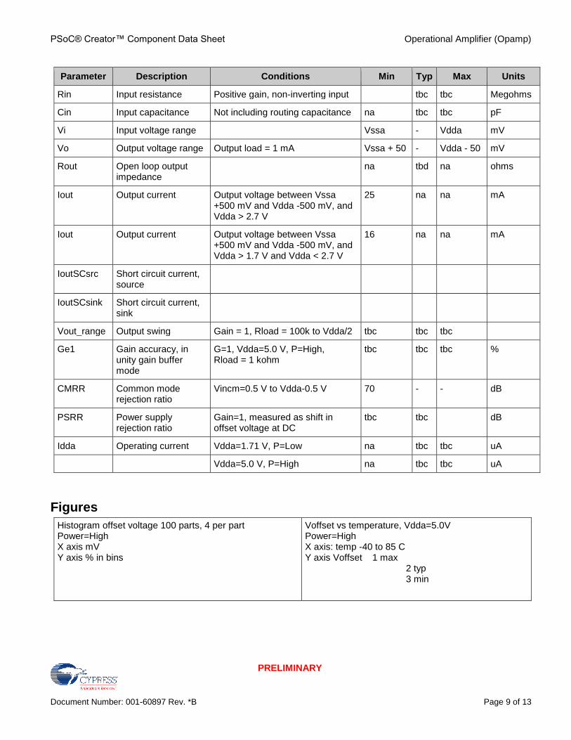
DC and AC Electrical Characteristics
The following values are based on characterization data. Specifications are valid for -40° C ≤ TA ≤ 85° C and TJ ≤ 100° C except where noted. Unless otherwise specified in the tables below, all Typical values are for TA = 25° C, Vdda = 5.0 V, Power = High, output referenced to analog ground, Vssa.
5.0 V/3.3 V DC Electrical Characteristics
Parameter Description Conditions Min Typ Max Units
Vos Input Offset Voltage Vdda=3.3 V, 25 C, P=Slow na 0.5 2 mV
Vdda=3.3 V, 25 C, P=Low na 0.5 2 mV
Vdda=3.3 V, 25 C, P=Med na 0.5 2 mV
Vdda=3.3 V, 25 C, P=High na 0.5 2 mV
TCVos Temp. coeff. input offset voltage, absolute value
P=Slow na tbc tbc uV/°C
P=Low na tbc tbc uV/°C
P=Med na tbc tbc uV/°C
P=High na tbc tbc uV/°C
AVOL Open Loop Gain P=Slow, Cload=15pF tbc tbc na dB
P=Low, Cload=15pF tbc tbc na dB
P=Med, Cload=15pF tbc tbc na dB
P=High, Cload=15pF tbc tbc na dB
PSoC® Creator™ Component Data Sheet Operational Amplifier (Opamp)
Document Number: 001-60897 Rev. *B Page 9 of 13
PRELIMINARY
Parameter Description Conditions Min Typ Max Units
Rin Input resistance Positive gain, non-inverting input tbc tbc Megohms
Cin Input capacitance Not including routing capacitance na tbc tbc pF
Vi Input voltage range Vssa - Vdda mV
Vo Output voltage range Output load = 1 mA Vssa + 50 - Vdda - 50 mV
Rout Open loop output impedance
na tbd na ohms
Iout Output current Output voltage between Vssa +500 mV and Vdda -500 mV, and Vdda > 2.7 V
25 na na mA
Iout Output current Output voltage between Vssa +500 mV and Vdda -500 mV, and Vdda > 1.7 V and Vdda < 2.7 V
16 na na mA
IoutSCsrc Short circuit current, source
IoutSCsink Short circuit current, sink
Vout_range Output swing Gain = 1, Rload = 100k to Vdda/2 tbc tbc tbc
Ge1 Gain accuracy, in unity gain buffer mode
G=1, Vdda=5.0 V, P=High, Rload = 1 kohm
tbc tbc tbc %
CMRR Common mode rejection ratio
Vincm=0.5 V to Vdda-0.5 V 70 - - dB
PSRR Power supply rejection ratio
Gain=1, measured as shift in offset voltage at DC
tbc tbc dB
Idda Operating current Vdda=1.71 V, P=Low na tbc tbc uA
Vdda=5.0 V, P=High na tbc tbc uA
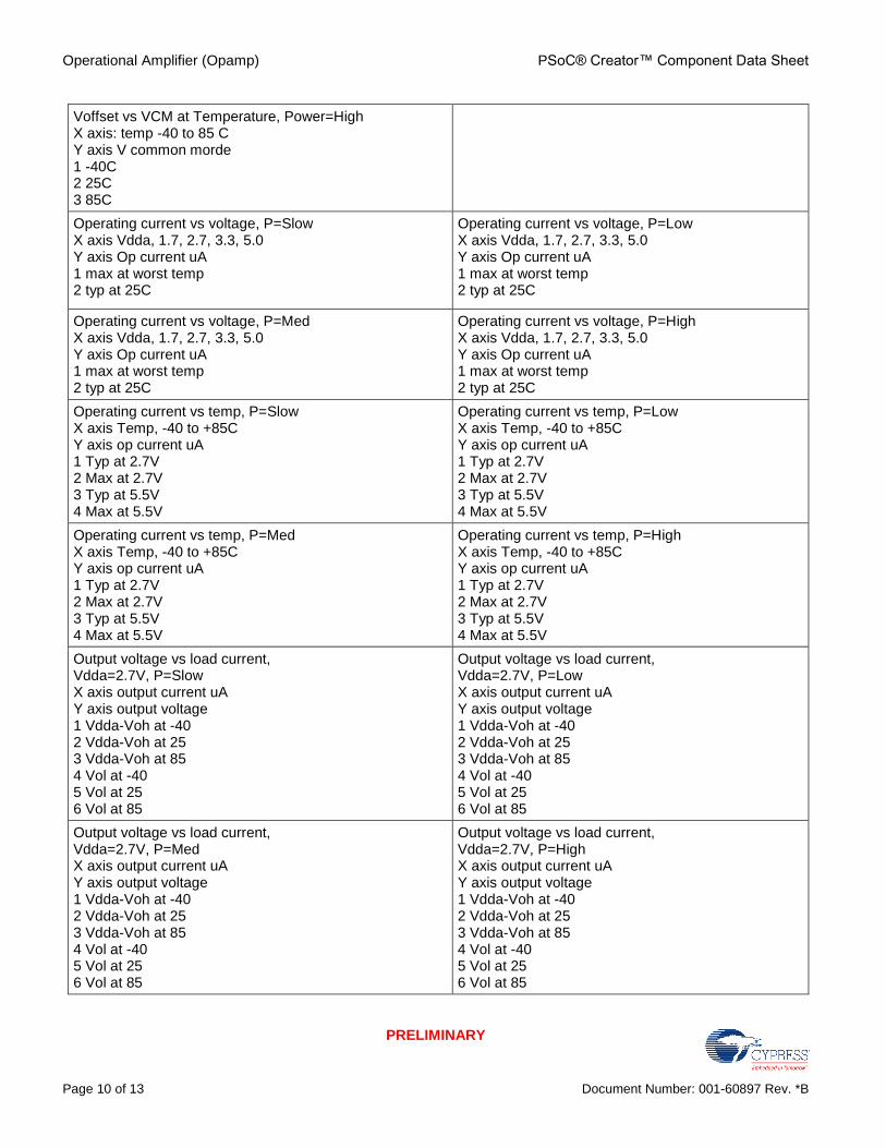
Figures
Histogram offset voltage 100 parts, 4 per part Power=High X axis mV Y axis % in bins
Voffset vs temperature, Vdda=5.0V Power=High X axis: temp -40 to 85 C Y axis Voffset 1 max 2 typ 3 min
Operational Amplifier (Opamp) PSoC® Creator™ Component Data Sheet
Page 10 of 13 Document Number: 001-60897 Rev. *B
PRELIMINARY
Voffset vs VCM at Temperature, Power=High X axis: temp -40 to 85 C Y axis V common morde 1 -40C 2 25C 3 85C
Operating current vs voltage, P=Slow X axis Vdda, 1.7, 2.7, 3.3, 5.0 Y axis Op current uA 1 max at worst temp 2 typ at 25C
Operating current vs voltage, P=Low X axis Vdda, 1.7, 2.7, 3.3, 5.0 Y axis Op current uA 1 max at worst temp 2 typ at 25C
Operating current vs voltage, P=Med X axis Vdda, 1.7, 2.7, 3.3, 5.0 Y axis Op current uA 1 max at worst temp 2 typ at 25C
Operating current vs voltage, P=High X axis Vdda, 1.7, 2.7, 3.3, 5.0 Y axis Op current uA 1 max at worst temp 2 typ at 25C
Operating current vs temp, P=Slow X axis Temp, -40 to +85C Y axis op current uA 1 Typ at 2.7V 2 Max at 2.7V 3 Typ at 5.5V 4 Max at 5.5V
Operating current vs temp, P=Low X axis Temp, -40 to +85C Y axis op current uA 1 Typ at 2.7V 2 Max at 2.7V 3 Typ at 5.5V 4 Max at 5.5V
Operating current vs temp, P=Med X axis Temp, -40 to +85C Y axis op current uA 1 Typ at 2.7V 2 Max at 2.7V 3 Typ at 5.5V 4 Max at 5.5V
Operating current vs temp, P=High X axis Temp, -40 to +85C Y axis op current uA 1 Typ at 2.7V 2 Max at 2.7V 3 Typ at 5.5V 4 Max at 5.5V
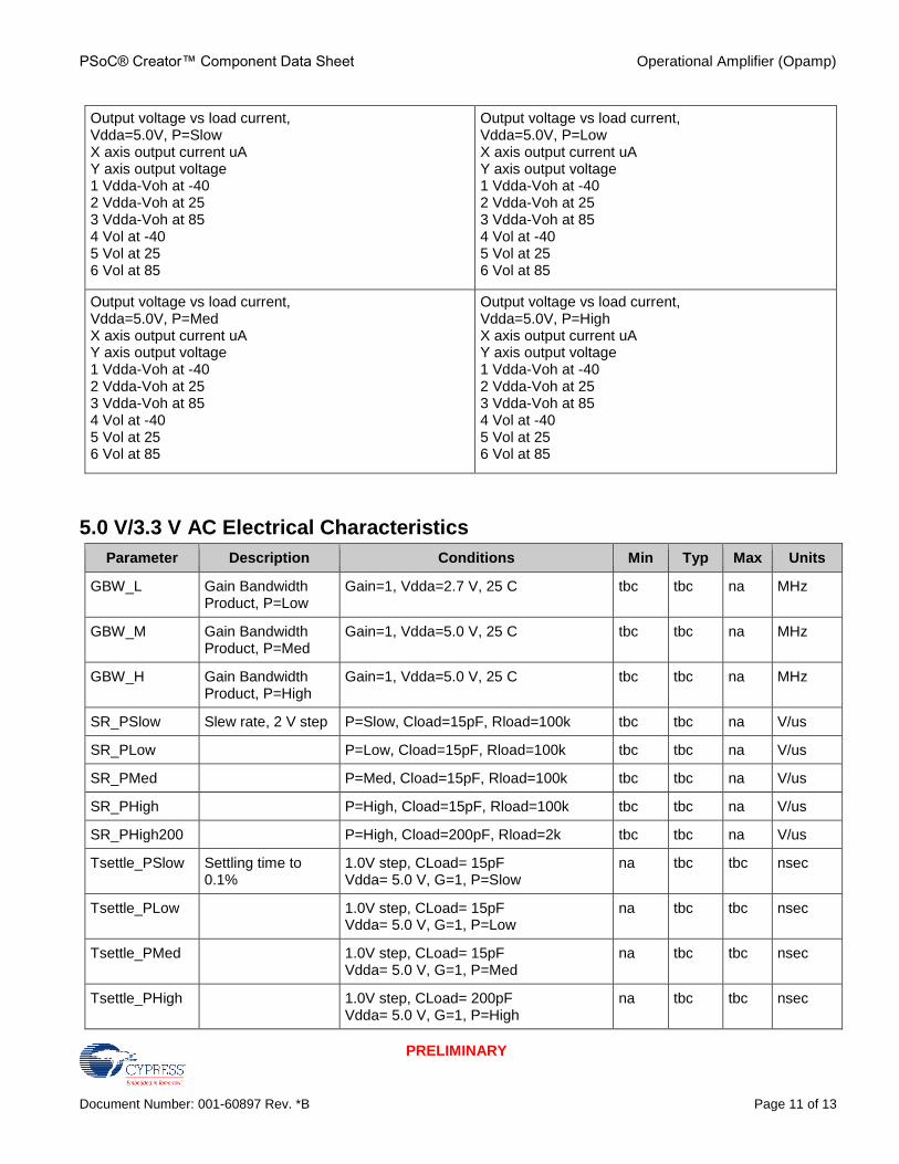
Output voltage vs load current, Vdda=2.7V, P=Slow X axis output current uA Y axis output voltage 1 Vdda-Voh at -40 2 Vdda-Voh at 25 3 Vdda-Voh at 85 4 Vol at -40 5 Vol at 25 6 Vol at 85
Output voltage vs load current, Vdda=2.7V, P=Low X axis output current uA Y axis output voltage 1 Vdda-Voh at -40 2 Vdda-Voh at 25 3 Vdda-Voh at 85 4 Vol at -40 5 Vol at 25 6 Vol at 85
Output voltage vs load current, Vdda=2.7V, P=Med X axis output current uA Y axis output voltage 1 Vdda-Voh at -40 2 Vdda-Voh at 25 3 Vdda-Voh at 85 4 Vol at -40 5 Vol at 25 6 Vol at 85
Output voltage vs load current, Vdda=2.7V, P=High X axis output current uA Y axis output voltage 1 Vdda-Voh at -40 2 Vdda-Voh at 25 3 Vdda-Voh at 85 4 Vol at -40 5 Vol at 25 6 Vol at 85
PSoC® Creator™ Component Data Sheet Operational Amplifier (Opamp)
Document Number: 001-60897 Rev. *B Page 11 of 13
PRELIMINARY
Output voltage vs load current, Vdda=5.0V, P=Slow X axis output current uA Y axis output voltage 1 Vdda-Voh at -40 2 Vdda-Voh at 25 3 Vdda-Voh at 85 4 Vol at -40 5 Vol at 25 6 Vol at 85
Output voltage vs load current, Vdda=5.0V, P=Low X axis output current uA Y axis output voltage 1 Vdda-Voh at -40 2 Vdda-Voh at 25 3 Vdda-Voh at 85 4 Vol at -40 5 Vol at 25 6 Vol at 85
Output voltage vs load current, Vdda=5.0V, P=Med X axis output current uA Y axis output voltage 1 Vdda-Voh at -40 2 Vdda-Voh at 25 3 Vdda-Voh at 85 4 Vol at -40 5 Vol at 25 6 Vol at 85
Output voltage vs load current, Vdda=5.0V, P=High X axis output current uA Y axis output voltage 1 Vdda-Voh at -40 2 Vdda-Voh at 25 3 Vdda-Voh at 85 4 Vol at -40 5 Vol at 25 6 Vol at 85
5.0 V/3.3 V AC Electrical Characteristics
Parameter Description Conditions Min Typ Max Units
GBW_L Gain Bandwidth Product, P=Low
Gain=1, Vdda=2.7 V, 25 C tbc tbc na MHz
GBW_M Gain Bandwidth Product, P=Med
Gain=1, Vdda=5.0 V, 25 C tbc tbc na MHz
GBW_H Gain Bandwidth Product, P=High
Gain=1, Vdda=5.0 V, 25 C tbc tbc na MHz
SR_PSlow Slew rate, 2 V step P=Slow, Cload=15pF, Rload=100k tbc tbc na V/us
SR_PLow P=Low, Cload=15pF, Rload=100k tbc tbc na V/us
SR_PMed P=Med, Cload=15pF, Rload=100k tbc tbc na V/us
SR_PHigh P=High, Cload=15pF, Rload=100k tbc tbc na V/us
SR_PHigh200 P=High, Cload=200pF, Rload=2k tbc tbc na V/us
Tsettle_PSlow Settling time to 0.1%
1.0V step, CLoad= 15pF Vdda= 5.0 V, G=1, P=Slow
na tbc tbc nsec
Tsettle_PLow 1.0V step, CLoad= 15pF Vdda= 5.0 V, G=1, P=Low
na tbc tbc nsec
Tsettle_PMed 1.0V step, CLoad= 15pF Vdda= 5.0 V, G=1, P=Med
na tbc tbc nsec
Tsettle_PHigh 1.0V step, CLoad= 200pF Vdda= 5.0 V, G=1, P=High
na tbc tbc nsec
Operational Amplifier (Opamp) PSoC® Creator™ Component Data Sheet
Page 12 of 13 Document Number: 001-60897 Rev. *B
PRELIMINARY
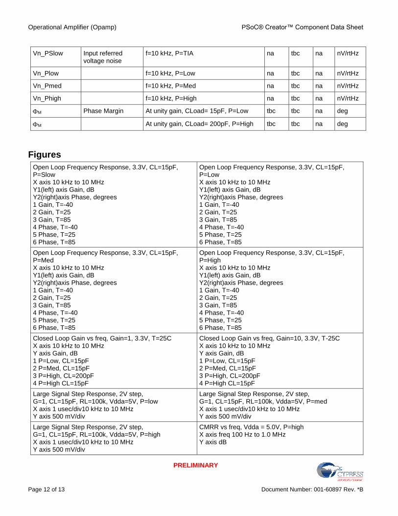
Vn_PSlow Input referred voltage noise
f=10 kHz, P=TIA na tbc na nV/rtHz
Vn_Plow f=10 kHz, P=Low na tbc na nV/rtHz
Vn_Pmed f=10 kHz, P=Med na tbc na nV/rtHz
Vn_Phigh f=10 kHz, P=High na tbc na nV/rtHz
M Phase Margin At unity gain, CLoad= 15pF, P=Low tbc tbc na deg
M At unity gain, CLoad= 200pF, P=High tbc tbc na deg
Figures
Open Loop Frequency Response, 3.3V, CL=15pF, P=Slow X axis 10 kHz to 10 MHz Y1(left) axis Gain, dB Y2(right)axis Phase, degrees 1 Gain, T=-40 2 Gain, T=25 3 Gain, T=85 4 Phase, T=-40 5 Phase, T=25 6 Phase, T=85
Open Loop Frequency Response, 3.3V, CL=15pF, P=Low X axis 10 kHz to 10 MHz Y1(left) axis Gain, dB Y2(right)axis Phase, degrees 1 Gain, T=-40 2 Gain, T=25 3 Gain, T=85 4 Phase, T=-40 5 Phase, T=25 6 Phase, T=85
Open Loop Frequency Response, 3.3V, CL=15pF, P=Med X axis 10 kHz to 10 MHz Y1(left) axis Gain, dB Y2(right)axis Phase, degrees 1 Gain, T=-40 2 Gain, T=25 3 Gain, T=85 4 Phase, T=-40 5 Phase, T=25 6 Phase, T=85
Open Loop Frequency Response, 3.3V, CL=15pF, P=High X axis 10 kHz to 10 MHz Y1(left) axis Gain, dB Y2(right)axis Phase, degrees 1 Gain, T=-40 2 Gain, T=25 3 Gain, T=85 4 Phase, T=-40 5 Phase, T=25 6 Phase, T=85
Closed Loop Gain vs freq, Gain=1, 3.3V, T=25C X axis 10 kHz to 10 MHz Y axis Gain, dB 1 P=Low, CL=15pF 2 P=Med, CL=15pF 3 P=High, CL=200pF 4 P=High CL=15pF
Closed Loop Gain vs freq, Gain=10, 3.3V, T-25C X axis 10 kHz to 10 MHz Y axis Gain, dB 1 P=Low, CL=15pF 2 P=Med, CL=15pF 3 P=High, CL=200pF 4 P=High CL=15pF
Large Signal Step Response, 2V step, G=1, CL=15pF, RL=100k, Vdda=5V, P=low X axis 1 usec/div10 kHz to 10 MHz Y axis 500 mV/div
Large Signal Step Response, 2V step, G=1, CL=15pF, RL=100k, Vdda=5V, P=med X axis 1 usec/div10 kHz to 10 MHz Y axis 500 mV/div
Large Signal Step Response, 2V step, G=1, CL=15pF, RL=100k, Vdda=5V, P=high X axis 1 usec/div10 kHz to 10 MHz Y axis 500 mV/div
CMRR vs freq, Vdda = 5.0V, P=high X axis freq 100 Hz to 1.0 MHz Y axis dB
PSoC® Creator™ Component Data Sheet Operational Amplifier (Opamp)
Document Number: 001-60897 Rev. *B Page 13 of 13
PRELIMINARY
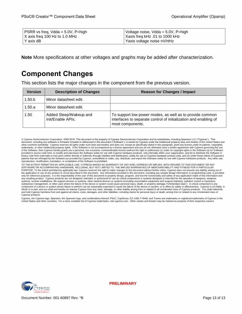
PSRR vs freq, Vdda = 5.0V, P=high X axis freq 100 Hz to 1.0 MHz Y axis dB
Voltage noise, Vdda = 5.0V, P=high Xaxis freq kHz .01 to 1000 kHz Yaxis voltage noise nV/rtHz
Note More specifications at other voltages and graphs may be added after characterization.
Component Changes
This section lists the major changes in the component from the previous version.
Version Description of Changes Reason for Changes / Impact
1.50.b Minor datasheet edit.
1.50.a Minor datasheet edit.
1.50 Added Sleep/Wakeup and Init/Enable APIs.
To support low power modes, as well as to provide common interfaces to separate control of initialization and enabling of most components.
© Cypress Semiconductor Corporation, 2009-2016. This document is the property of Cypress Semiconductor Corporation and its subsidiaries, including Spansion LLC (“Cypress”). This document, including any software or firmware included or referenced in this document (“Software”), is owned by Cypress under the intellectual property laws and treaties of the United States and other countries worldwide. Cypress reserves all rights under such laws and treaties and does not, except as specifically stated in this paragraph, grant any license under its patents, copyrights, trademarks, or other intellectual property rights. If the Software is not accompanied by a license agreement and you do not otherwise have a written agreement with Cypress governing the use of the Software, then Cypress hereby grants you a personal, non-exclusive, nontransferable license (without the right to sublicense) (1) under its copyright rights in the Software (a) for Software provided in source code form, to modify and reproduce the Software solely for use with Cypress hardware products, only internally within your organization, and (b) to distribute the Software in binary code form externally to end users (either directly or indirectly through resellers and distributors), solely for use on Cypress hardware product units, and (2) under those claims of Cypress’s patents that are infringed by the Software (as provided by Cypress, unmodified) to make, use, distribute, and import the Software solely for use with Cypress hardware products. Any other use, reproduction, modification, translation, or compilation of the Software is prohibited.
TO THE EXTENT PERMITTED BY APPLICABLE LAW, CYPRESS MAKES NO WARRANTY OF ANY KIND, EXPRESS OR IMPLIED, WITH REGARD TO THIS DOCUMENT OR ANY SOFTWARE OR ACCOMPANYING HARDWARE, INCLUDING, BUT NOT LIMITED TO, THE IMPLIED WARRANTIES OF MERCHANTABILITY AND FITNESS FOR A PARTICULAR PURPOSE. To the extent permitted by applicable law, Cypress reserves the right to make changes to this document without further notice. Cypress does not assume any liability arising out of the application or use of any product or circuit described in this document. Any information provided in this document, including any sample design information or programming code, is provided only for reference purposes. It is the responsibility of the user of this document to properly design, program, and test the functionality and safety of any application made of this information and any resulting product. Cypress products are not designed, intended, or authorized for use as critical components in systems designed or intended for the operation of weapons, weapons systems, nuclear installations, life-support devices or systems, other medical devices or systems (including resuscitation equipment and surgical implants), pollution control or hazardous substances management, or other uses where the failure of the device or system could cause personal injury, death, or property damage (“Unintended Uses”). A critical component is any component of a device or system whose failure to perform can be reasonably expected to cause the failure of the device or system, or to affect its safety or effectiveness. Cypress is not liable, in whole or in part, and you shall and hereby do release Cypress from any claim, damage, or other liability arising from or related to all Unintended Uses of Cypress products. You shall indemnify and hold Cypress harmless from and against all claims, costs, damages, and other liabilities, including claims for personal injury or death, arising from or related to any Unintended Uses of Cypress products.
Cypress, the Cypress logo, Spansion, the Spansion logo, and combinations thereof, PSoC, CapSense, EZ-USB, F-RAM, and Traveo are trademarks or registered trademarks of Cypress in the United States and other countries. For a more complete list of Cypress trademarks, visit cypress.com. Other names and brands may be claimed as property of their respective owners.