
FET AMPLIFIER
67
FET AMPLIFIER
-
Upload
khangminh22 -
Category
Documents
-
view
4 -
download
0
Transcript of FET AMPLIFIER

FET AMPLIFIER
ENGR. JESS RANGCASAJO
ECE321 INSTRUCTOR

INTRODUCTION
▶ Field-effect transistor amplifiers provide an excellent
voltage gain with the added feature of a high input
impedance. They are also low-power-consumption
configurations with good frequency range and minimal
size and weight.
▶ JFETs, depletion MOSFETs, and MESFETs can be used to
design amplifiers having similar voltage gains.
▶ The depletion MOSFET (MESFET) circuit, however, has a
much higher input impedance than a similar JFET
configuration.

INTRODUCTION
▶ Whereas a BJT device controls a large output (collector)
current by means of a relatively small input (base) current,
the FET device controls an output (drain) current by means
ofa small input (gate-voltage) voltage.
▶ In general, therefore, the BJT is a current-controlled device
and the FET is a voltage-controlled device.
▶ Because of the high input characteristic of FETs, the ac
equivalent model is somewhat simpler than that employed for
BJTs.
▶ Whereas the BJT has an amplification factor, ß (beta), the
FET has a transconductance factor, gm .

JFET SMALL-SIGNAL MODEL
The gate-to-source voltage controls the drain-to-source (channel)
current of a JFET.
The change in drain current that will result from a change in gate-to-source voltage
can be determined using the transconductance factor g m in the following manner:
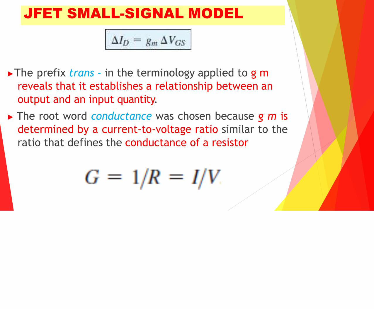
▶The prefix trans - in the terminology applied to g m
reveals that it establishes a relationship between an
output and an input quantity.
▶ The root word conductance was chosen because g m is
determined by a current-to-voltage ratio similar to the
ratio that defines the conductance of a resistor
JFET SMALL-SIGNAL MODEL
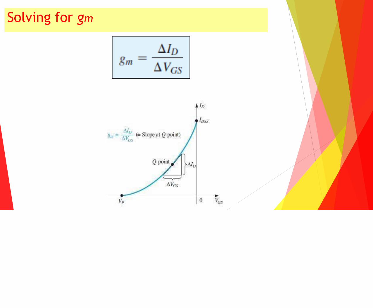
Solving for gm

Mathematical Definition of gm
The derivative of a function at a point is equal to the
slope of the tangent line drawn at that point.
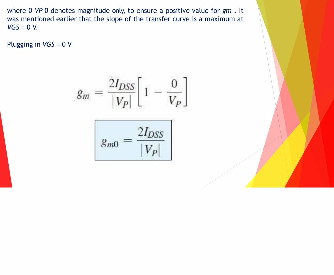
where 0 VP 0 denotes magnitude only, to ensure a positive value for gm . It
was mentioned earlier that the slope of the transfer curve is a maximum at
VGS = 0 V.
Plugging in VGS = 0 V

where the added subscript 0 reminds us that it is the
value of g m when VGS = 0 V
Equation 1
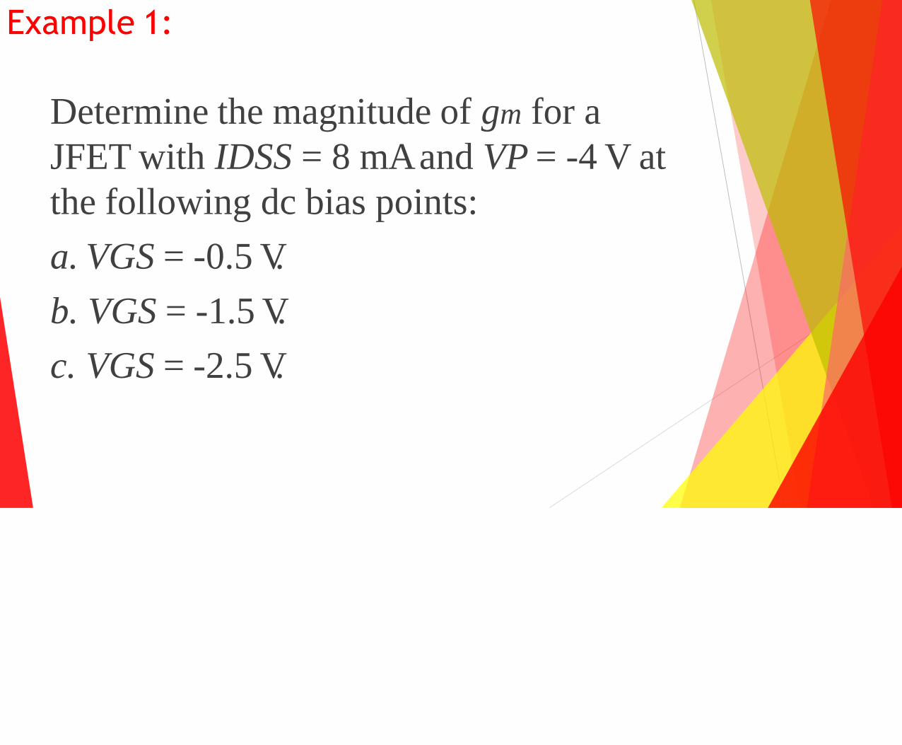
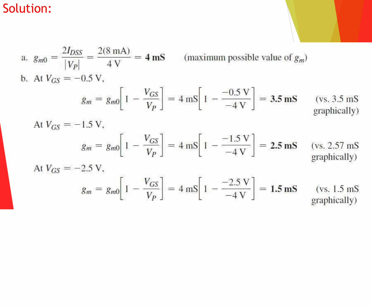
Example 1:
Determine the magnitude of gm for a
JFET with IDSS = 8 mA and VP = -4 V at
the following dc bias points:
a. VGS = -0.5 V.
b. VGS = -1.5 V.
c. VGS = -2.5 V.

Solution:

Solution:
Note the decrease in gm as VGS approaches VP

Example 2:
For the JFET having the transfer
characteristics of Example 1 :
a. Find the maximum value of g m .
b.Find the value of g m at each
operating point of Example 1 using
Eq. (1) and compare with the
graphical results.
Solution:
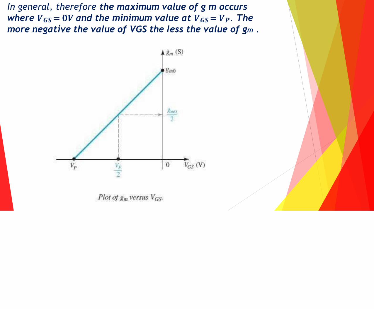
In general, therefore the maximum value of g m occurs
where 𝑽𝑮𝑺 = 𝟎𝑽 and the minimum value at 𝑽𝑮𝑺 = 𝑽𝑷. The
more negative the value of VGS the less the value of gm .
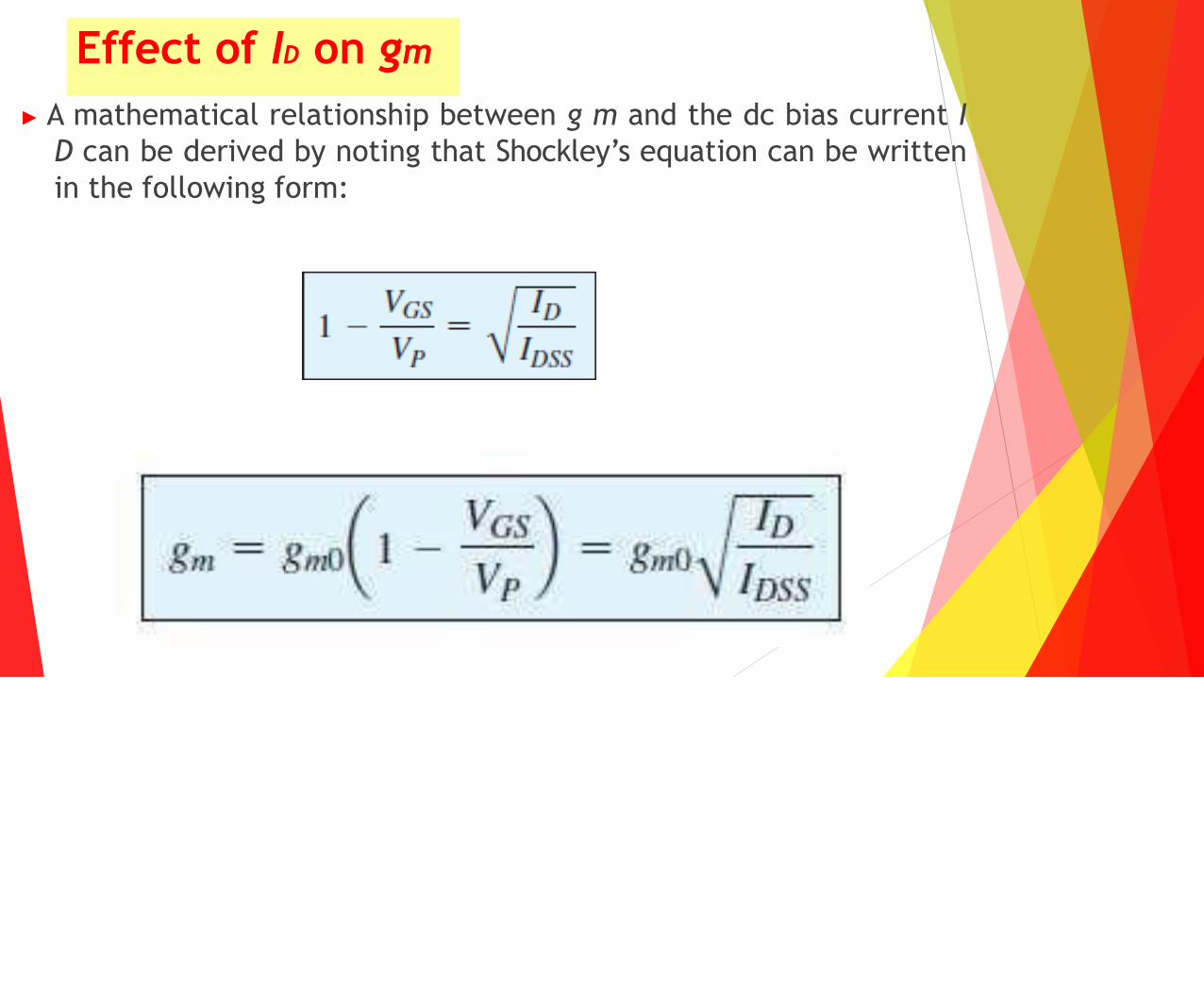
Effect of ID on gm
▶ A mathematical relationship between g m and the dc bias current I
D can be derived by noting that Shockley’s equation can be written
in the following form:
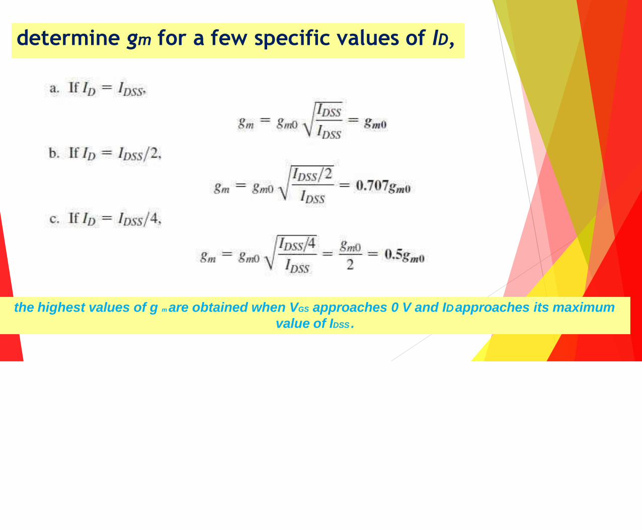
determine gm for a few specific values of ID,
the highest values of g m are obtained when VGS approaches 0 V and ID approaches its maximum
value of IDSS .
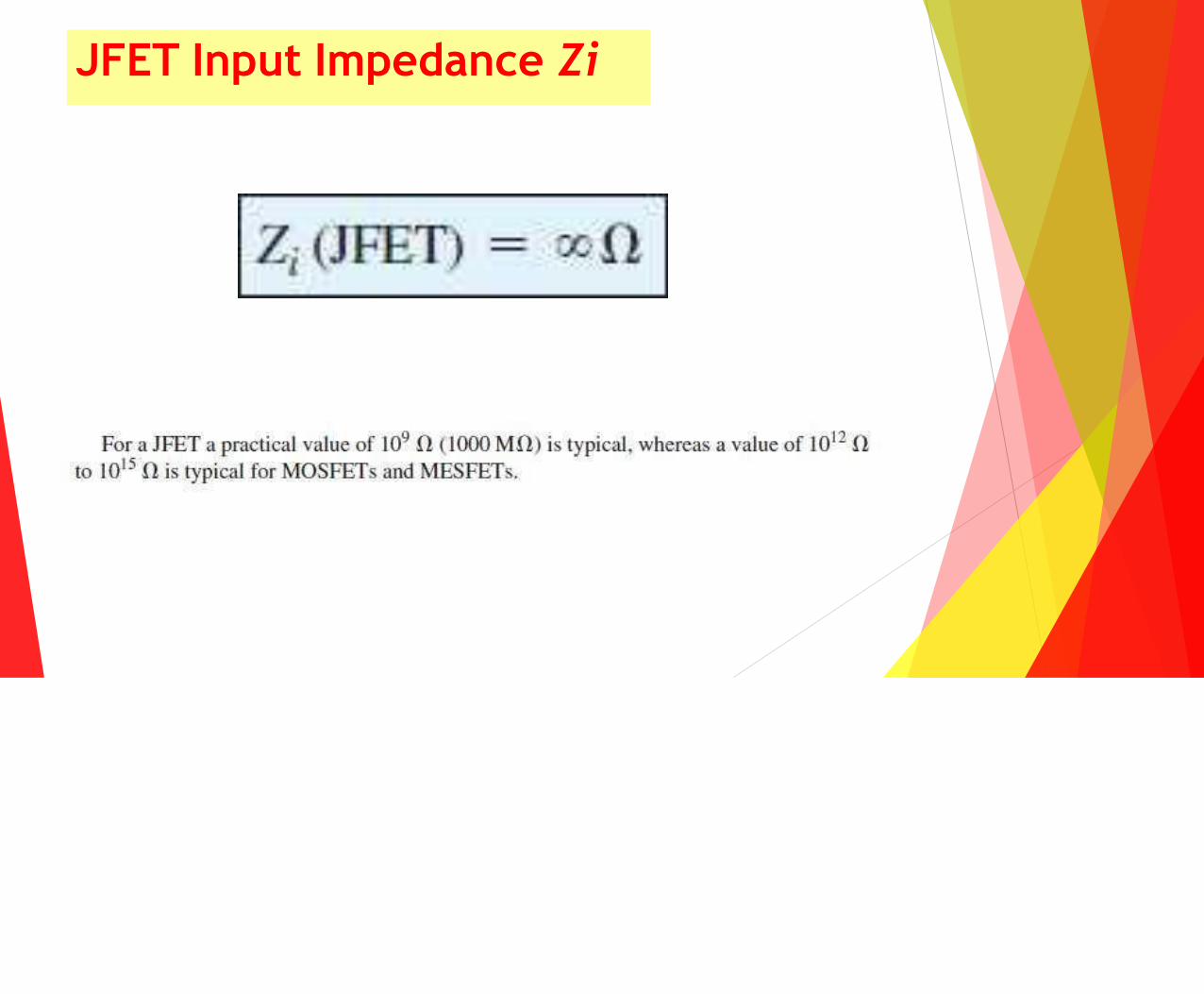
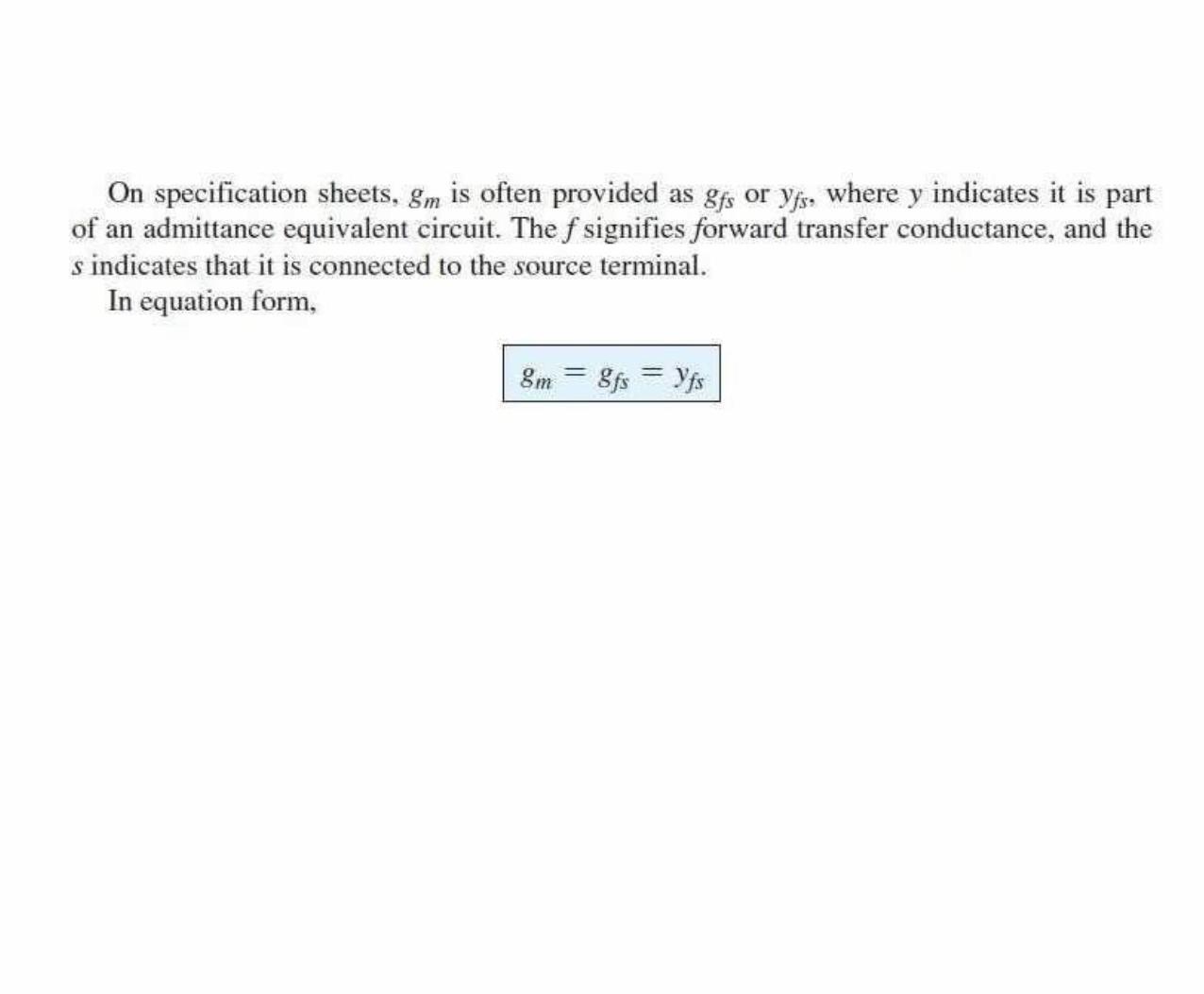
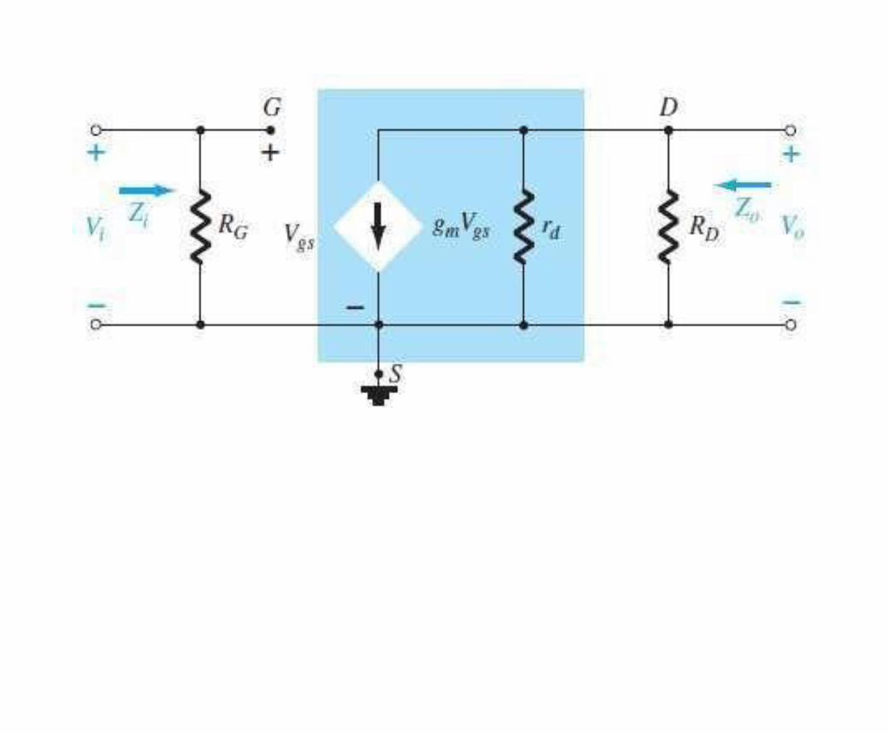
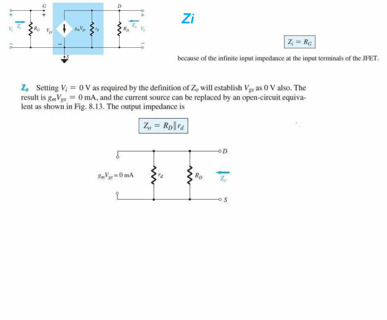
JFET Input Impedance Zi
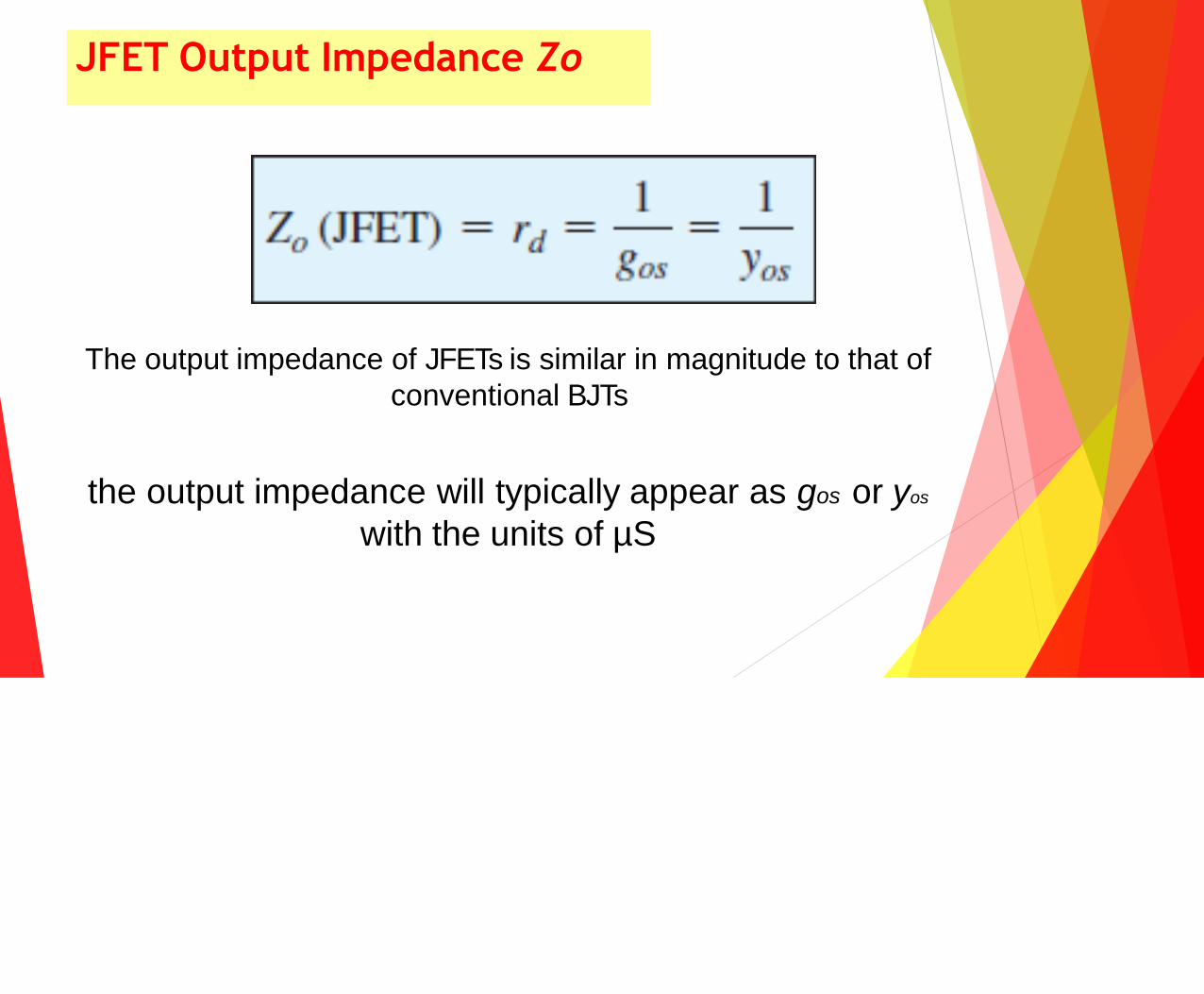
JFET Output Impedance Zo
The output impedance of JFETs is similar in magnitude to that of
conventional BJTs
the output impedance will typically appear as gos or yos
with the units of µS

The parameter yos is a component of an admittance equivalent
circuit , with the subscript o signifying an output network parameter
and s the terminal ( source) to which it is attached in the model.
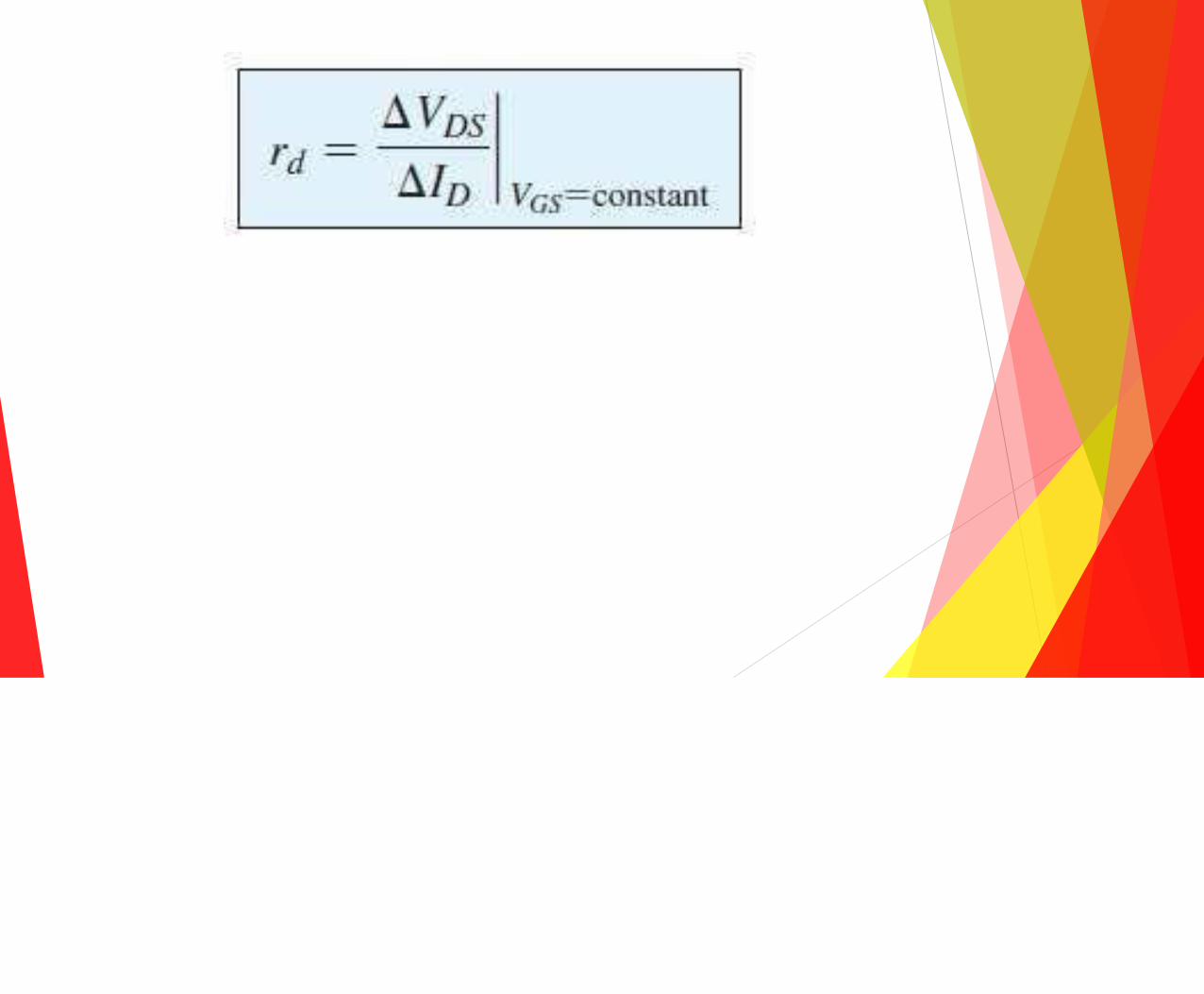
The output impedance is defined on the characteristics as the
slope of the horizontal characteristic curve at the point of
operation.
The more horizontal the curve, the greater is the output
impedance.
If it is perfectly horizontal, the ideal situation is on hand with the
output impedance being infinite (an open circuit)—an often
applied approximation.
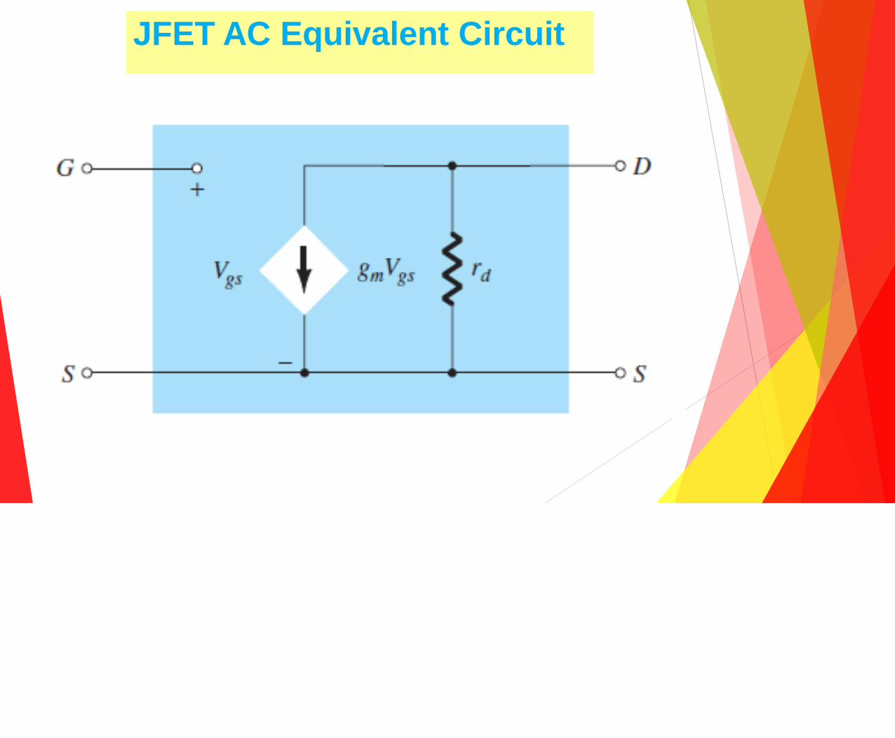
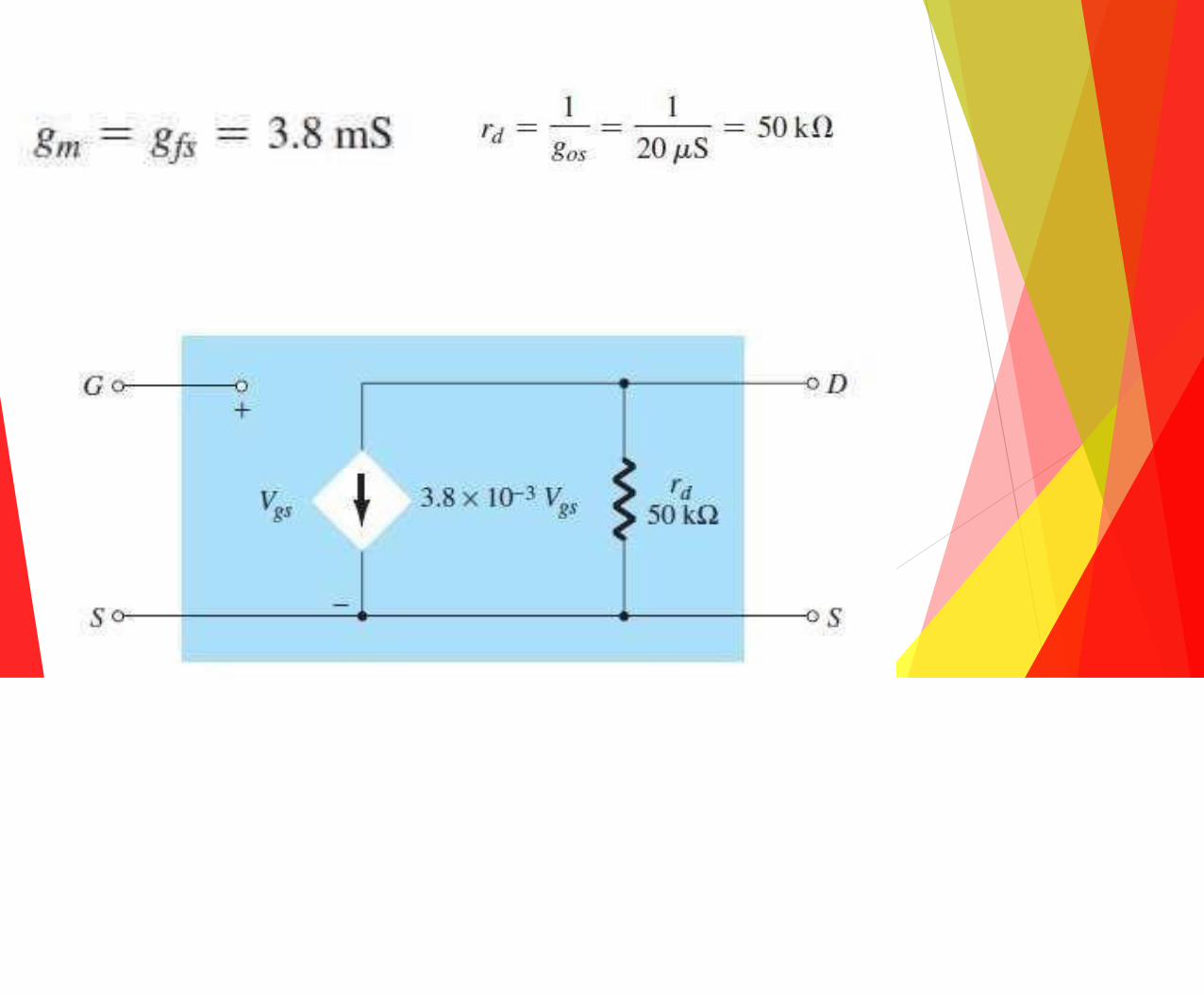
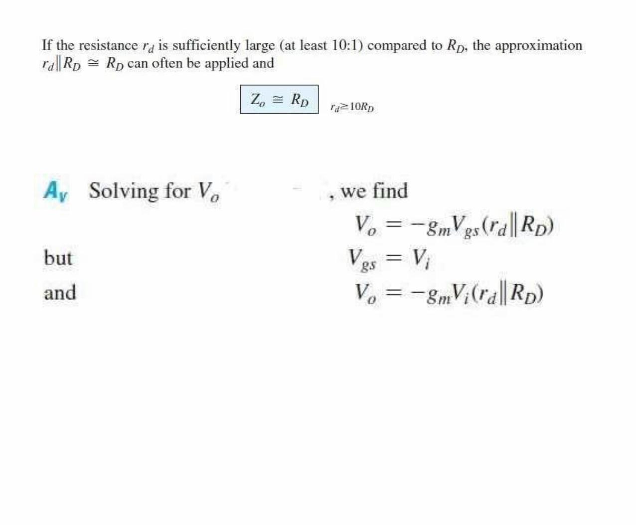
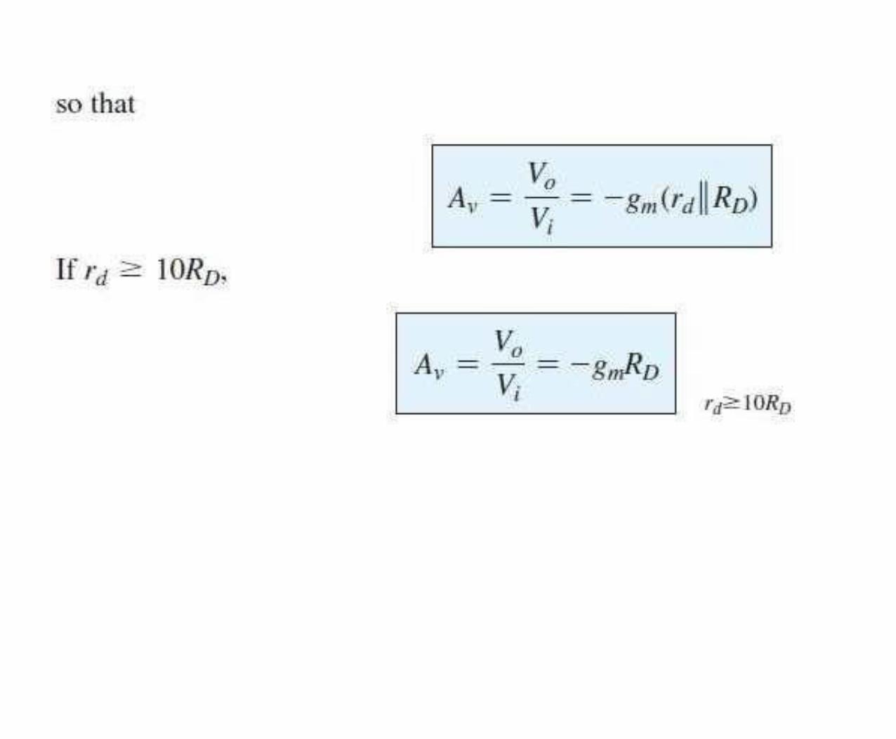
JFET AC Equivalent Circuit
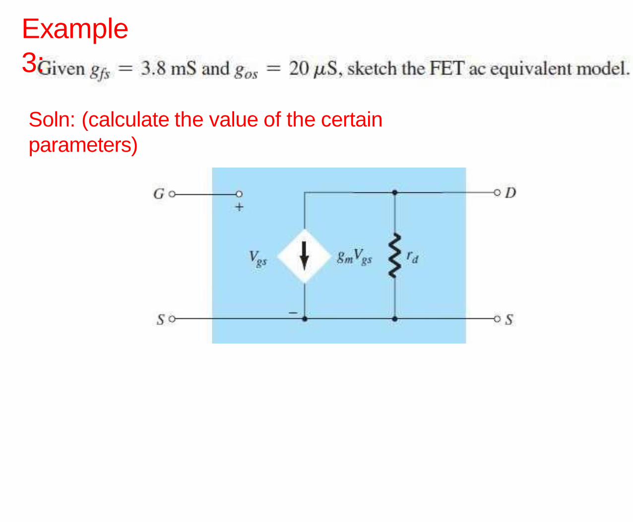
Soln: (calculate the value of the certain
parameters)
Example
3:

FET CONFIGURATION:
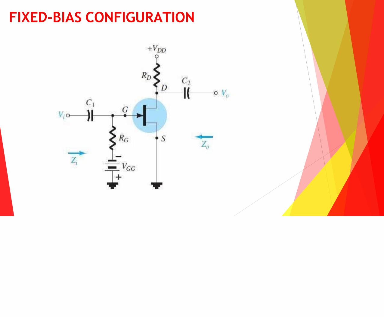
FIXED-BIAS CONFIGURATION

Zi

Thank You!

Reference
▶ Boylestad, R. L., Nashelsky, L., & Li, L. (2002). Electronic devices and circuit
theory (Vol. 11). Englewood Cliffs, NJ: Prentice Hall.
▶ Boylestad, R. L. (2010). Introductory circuit analysis. Pearson Education.
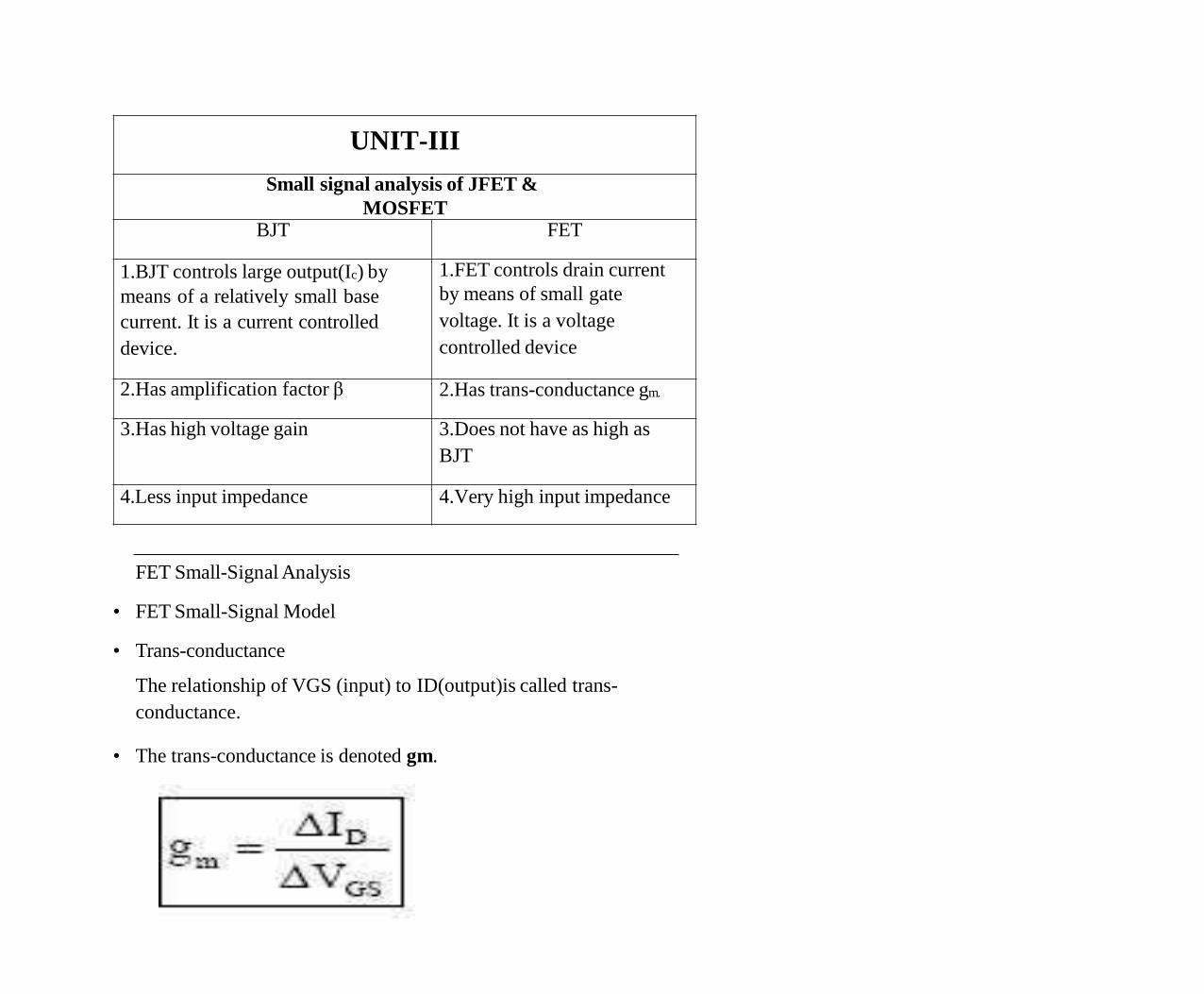
UNIT-III
Small signal analysis of JFET &
MOSFET BJT FET
1.BJT controls large output(Ic) by
means of a relatively small base
current. It is a current controlled
device.
1.FET controls drain current
by means of small gate
voltage. It is a voltage
controlled device
2.Has amplification factor β 2.Has trans-conductance gm.
3.Has high voltage gain 3.Does not have as high as
BJT
4.Less input impedance 4.Very high input impedance
FET Small-Signal Analysis
• FET Small-Signal Model
• Trans-conductance
The relationship of VGS (input) to ID(output)is called trans-
conductance.
• The trans-conductance is denoted gm.

Definition of gm using transfer characteristics
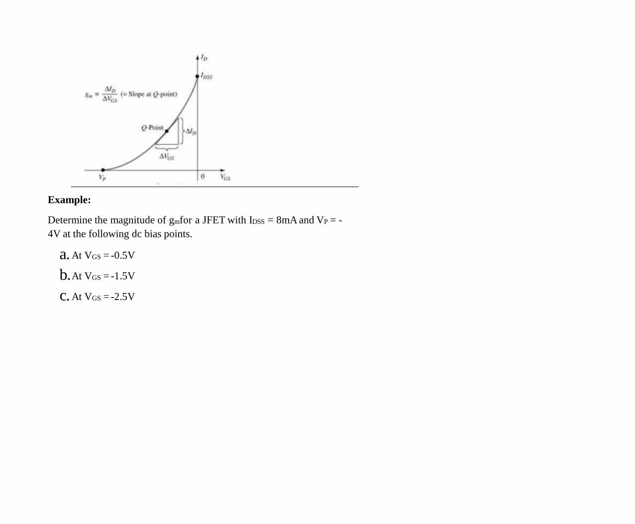
Example:
Determine the magnitude of gmfor a JFET with IDSS = 8mA and VP = -
4V at the following dc bias points.
a.At VGS = -0.5V
b.At VGS = -1.5V
c.At VGS = -2.5V
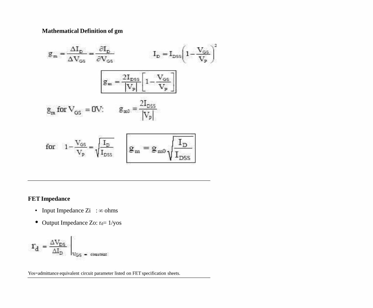
Mathematical Definition of gm
FET Impedance
• Input Impedance Zi : ∞ ohms
• Output Impedance Zo: rd= 1/yos
Yos=admittance equivalent circuit parameter listed on FET specification sheets.
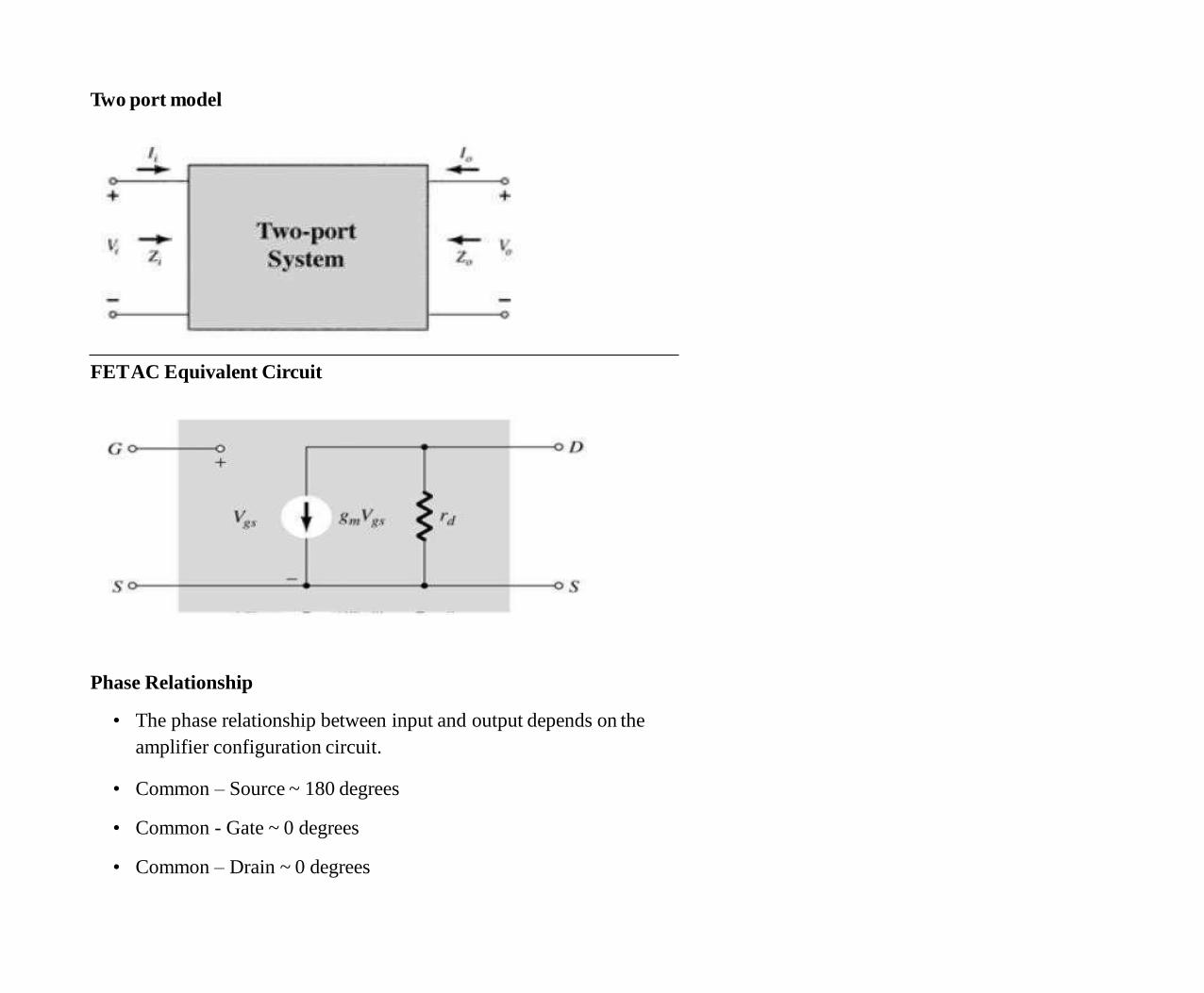
Two port model
FET AC Equivalent Circuit
Phase Relationship
• The phase relationship between input and output depends on the
amplifier configuration circuit.
• Common – Source ~ 180 degrees
• Common - Gate ~ 0 degrees
• Common – Drain ~ 0 degrees
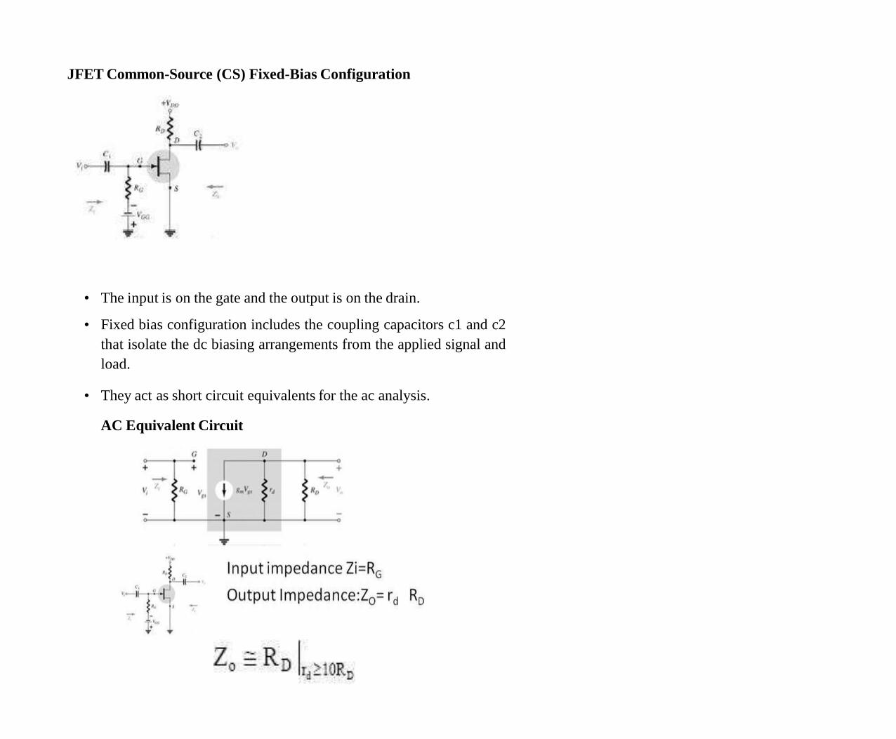
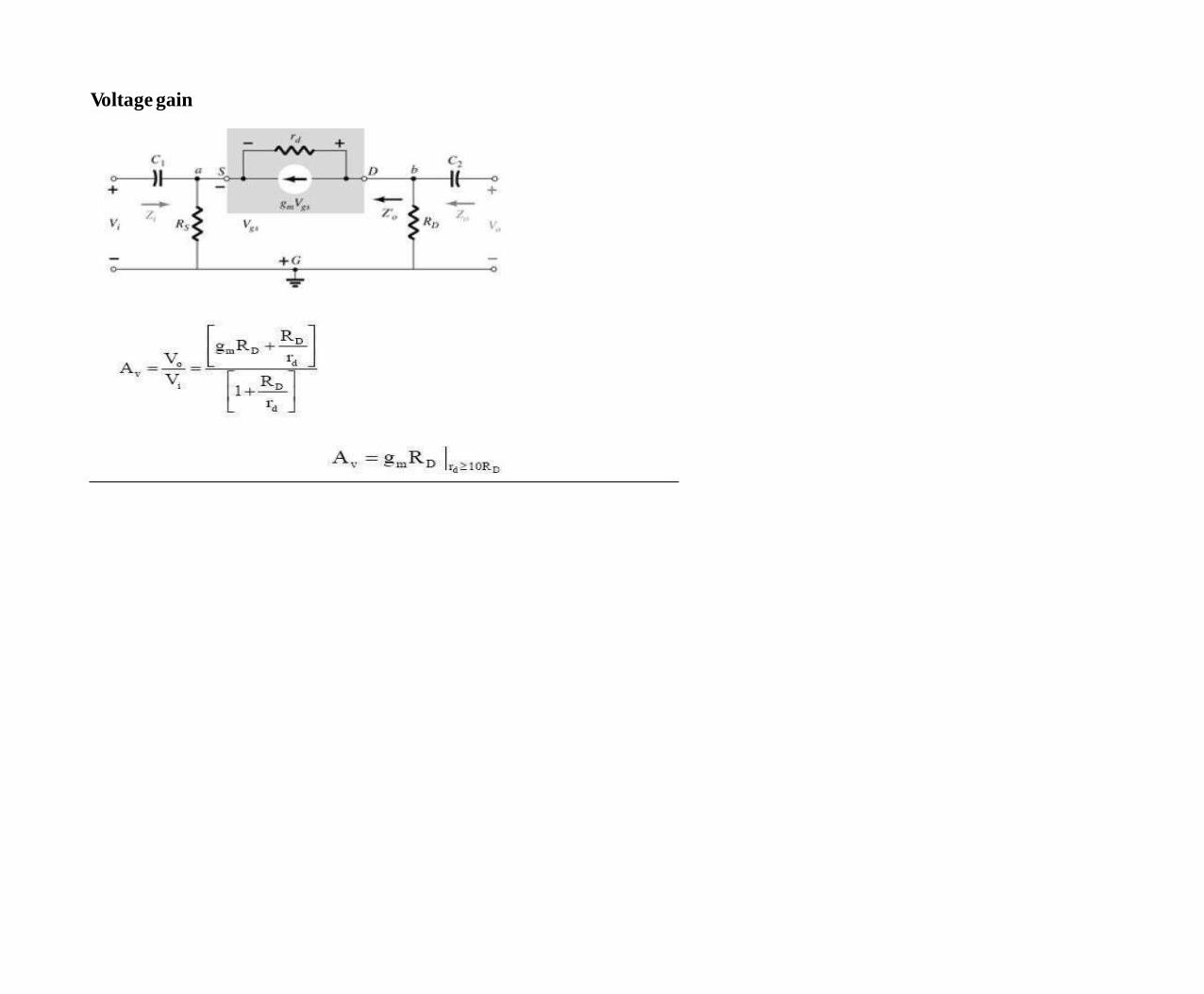
JFET Common-Source (CS) Fixed-Bias Configuration
• The input is on the gate and the output is on the drain.
• Fixed bias configuration includes the coupling capacitors c1 and c2
that isolate the dc biasing arrangements from the applied signal and
load.
• They act as short circuit equivalents for the ac analysis.
AC Equivalent Circuit
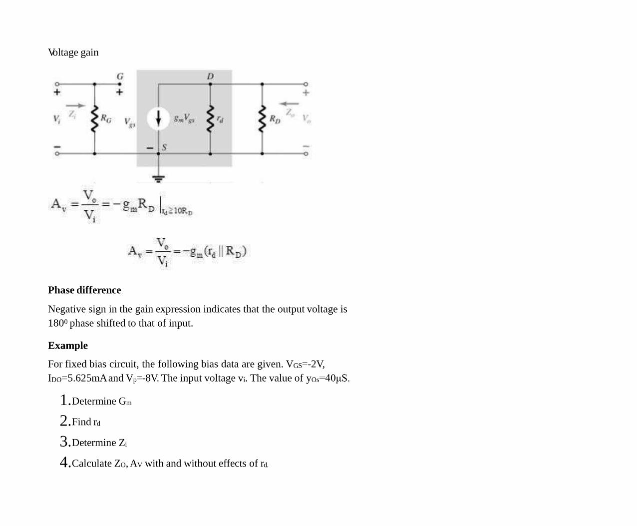
Voltage gain
Phase difference
Negative sign in the gain expression indicates that the output voltage is
1800 phase shifted to that of input.
Example
For fixed bias circuit, the following bias data are given. VGS=-2V,
IDO=5.625mA and Vp=-8V. The input voltage vi. The value of yOs=40μS.
1.Determine Gm
2.Find rd
3.Determine Zi
4.Calculate ZO, AV with and without effects of rd.
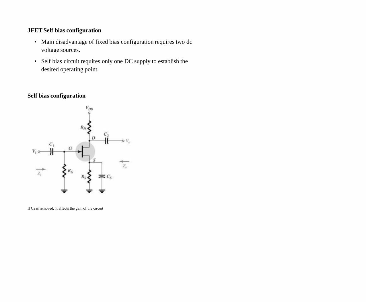
JFET Self bias configuration
• Main disadvantage of fixed bias configuration requires two dc
voltage sources.
• Self bias circuit requires only one DC supply to establish the
desired operating point.
Self bias configuration
If Cs is removed, it affects the gain of the circuit

AC Equivalent Circuit
•
• The capacitor across the source resistance assumes its short circuit
equivalent for dc allowing RS to define the operating point.
• Under ac conditions the capacitors assumes short circuit state and
short circuits the Rs.
If RS is left un-shorted, then ac gain will be reduced.
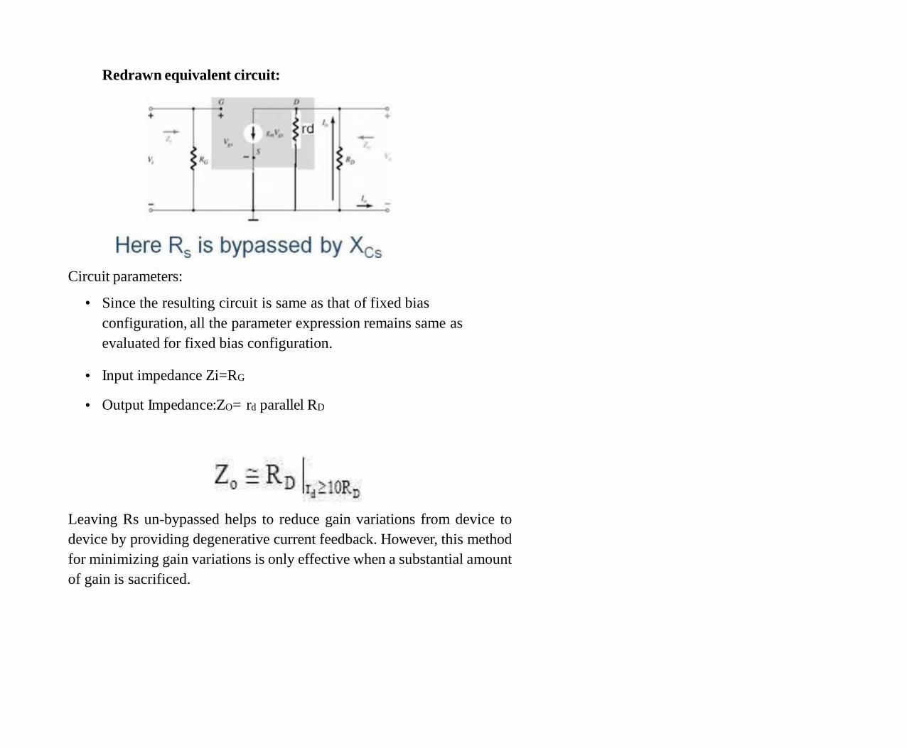
Redrawn equivalent circuit:
Circuit parameters:
•
•
• Since the resulting circuit is same as that of fixed bias
configuration, all the parameter expression remains same as
evaluated for fixed bias configuration.
Input impedance Zi=RG
Output Impedance:ZO= rd parallel RD
Leaving Rs un-bypassed helps to reduce gain variations from device to
device by providing degenerative current feedback. However, this method
for minimizing gain variations is only effective when a substantial amount
of gain is sacrificed.
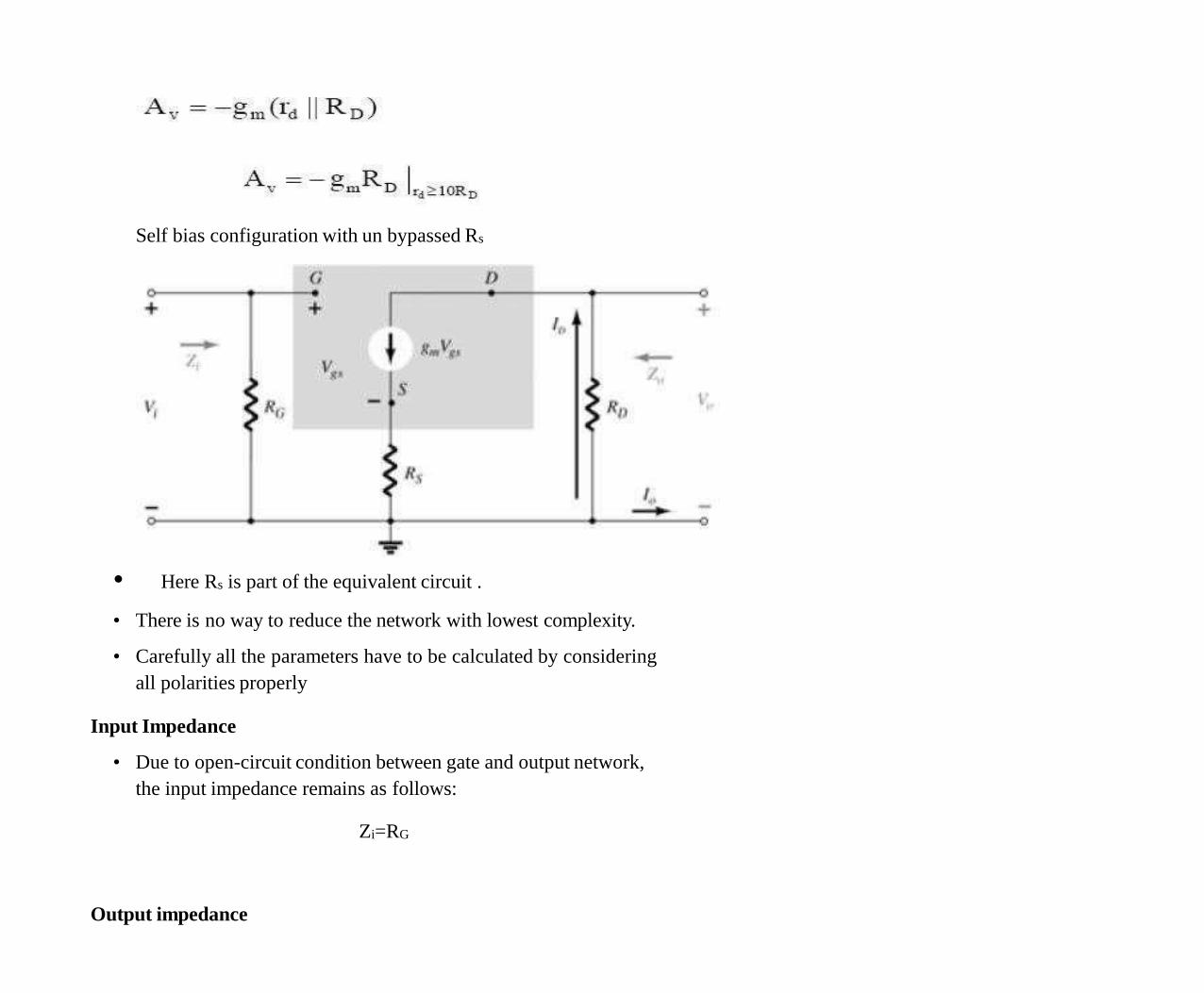
Self bias configuration with un bypassed Rs
• Here Rs is part of the equivalent circuit .
• There is no way to reduce the network with lowest complexity.
• Carefully all the parameters have to be calculated by considering
all polarities properly
Input Impedance
• Due to open-circuit condition between gate and output network,
the input impedance remains as follows:
Zi=RG
Output impedance
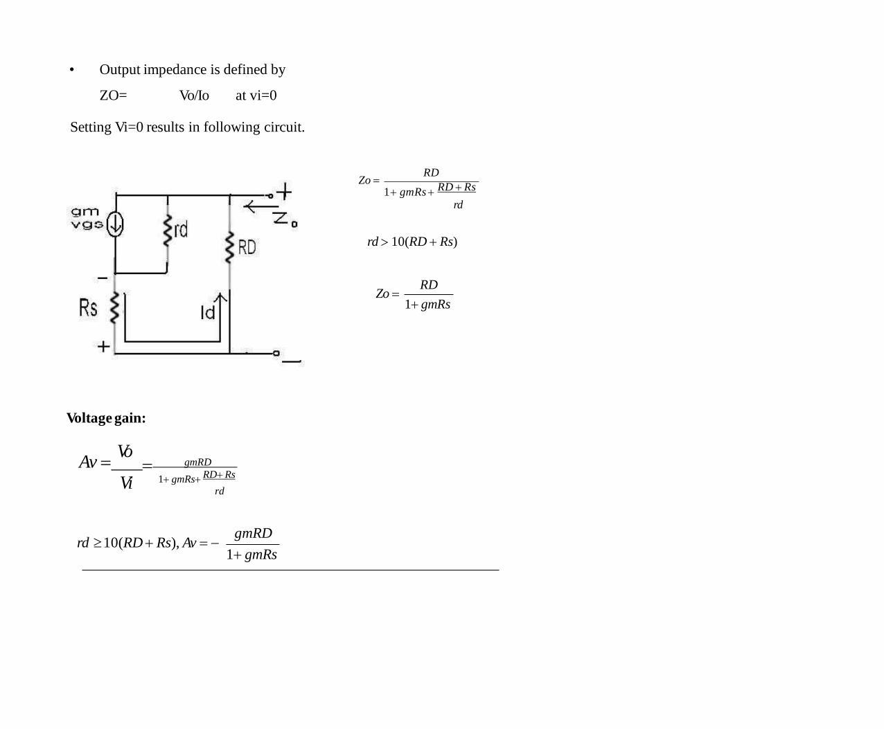
• Output impedance is defined by
ZO= Vo/Io at vi=0
Setting Vi=0 results in following circuit.
Zo RD
1 gmRs RD Rs
rd
rd 10(RD Rs)
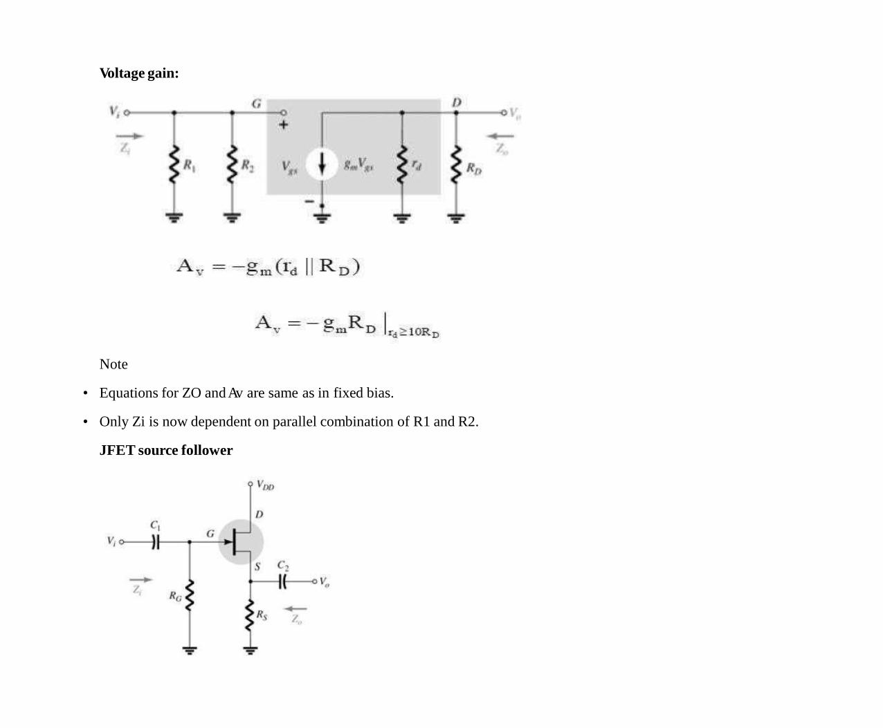
Voltage gain:
Zo RD
1 gmRs
Vo
Vi
Av gmRD
1 gmRs RD Rs
rd
rd 10(RD Rs), Av gmRD
1 gmRs
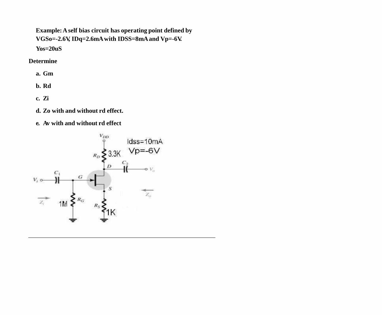
Example: A self bias circuit has operating point defined by
VGSo=-2.6V, IDq=2.6mA with IDSS=8mA and Vp=-6V.
Yos=20uS
Determine
a. Gm
b. Rd
c. Zi
d. Zo with and without rd effect.
e. Av with and without rd effect
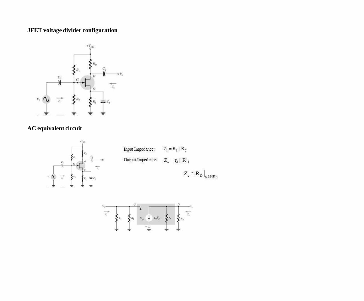
JFET voltage divider configuration
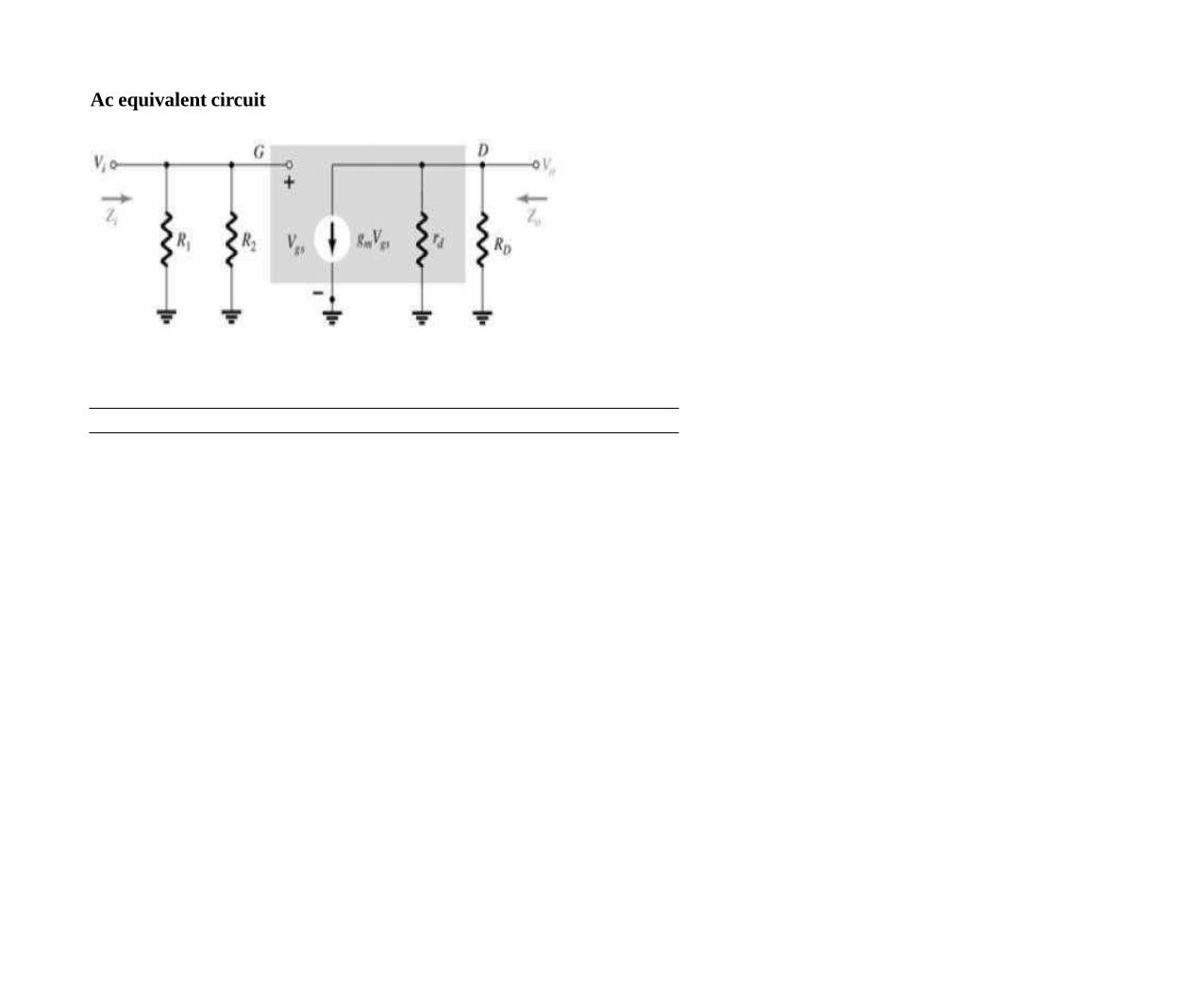
AC equivalent circuit
Voltage gain:
Note
• Equations for ZO and Av are same as in fixed bias.
• Only Zi is now dependent on parallel combination of R1 and R2.
JFET source follower

In a CD amplifier configuration the input is on the gate, but
the output is from the source.
AC equivalent circuit
Input and output impedance:
• Input impedance : Zi=RG
• Output impedance :
setting Vi=0V will result in the gate terminal being connected
directly to ground as shown in figure below.
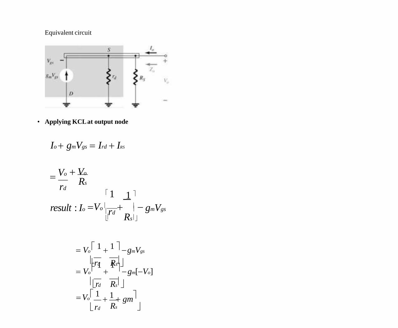
Equivalent circuit
• Applying KCL at output node
Io gmVgs Ird IRS
Vo
rd
Vo
Rs
1 1
result : Io Vo rd
Rs
gmVgs
Vo 1 1 gmVgs
r1d R1 s
Vo gm[Vo]
rd Rs
Vo 1
1 gm
Rs rd
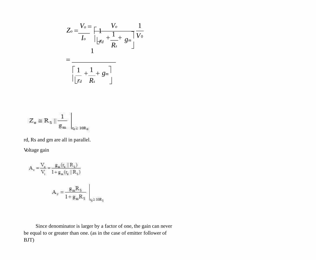
Vo Zo 1
rd Io
1
1
Vo
Rs
1
gm V 0
1
rd Rs
1 gm
rd, Rs and gm are all in parallel.
Voltage gain
Since denominator is larger by a factor of one, the gain can never
be equal to or greater than one. (as in the case of emitter follower of
BJT)
Example:
A dc analysis of the source follower has resulted in VGS=-2.86V and
Io=4.56mA.
Determine
a. gm
b. Zi
c. rd
d. Calculate Zo with and without effect of rd.
e. Calculate Av with and without effect of rd.
Compare the results.
Given IDSS=16mA, Vp=-4V, yos=25μS.
The coupling capacitors used are 0.05μF.
JFET common gate configuration
The input is on source and the output is on the drain.
Same as the common base in BJT

AC equivalent circuit
Impedances:
Voltage gain
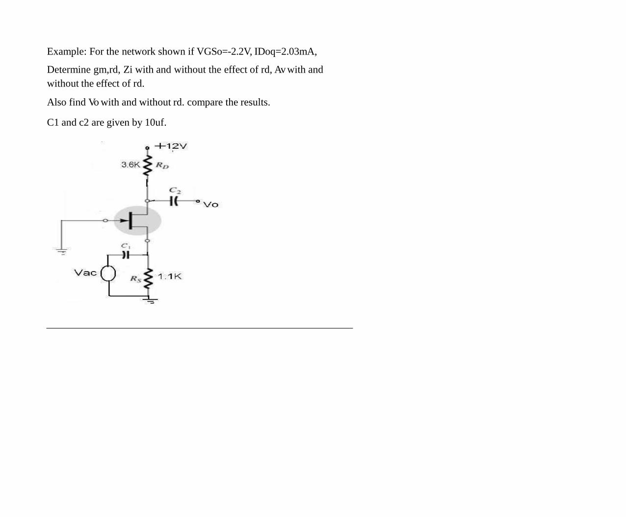
Example: For the network shown if VGSo=-2.2V, IDoq=2.03mA,
Determine gm,rd, Zi with and without the effect of rd, Av with and
without the effect of rd.
Also find Vo with and without rd. compare the results.
C1 and c2 are given by 10uf.
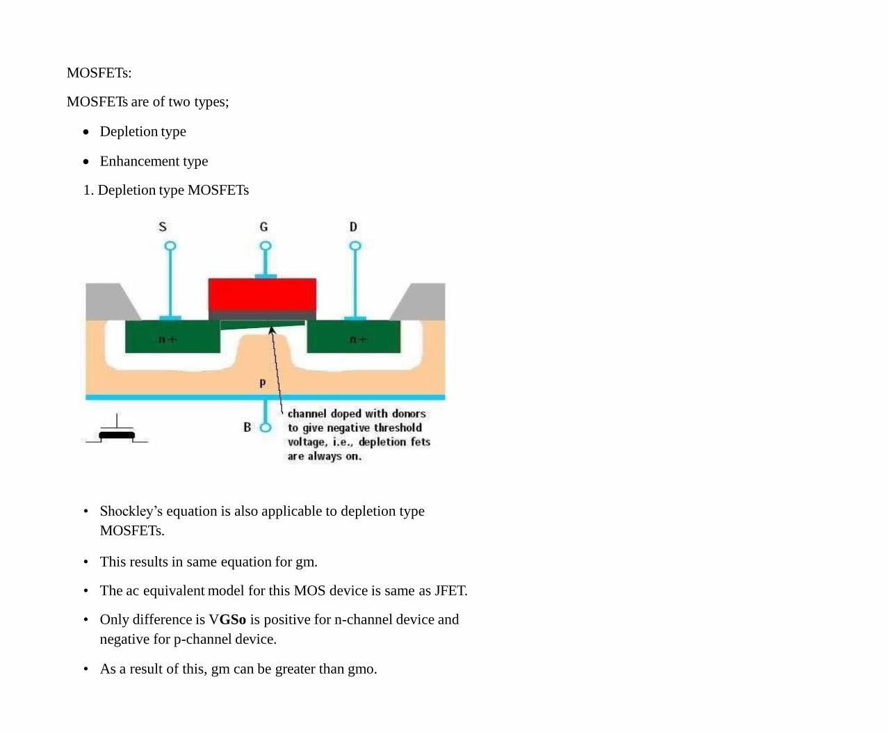
MOSFETs:
MOSFETs are of two types;
Depletion type
Enhancement type
1. Depletion type MOSFETs
• Shockley’s equation is also applicable to depletion type
MOSFETs.
• This results in same equation for gm.
• The ac equivalent model for this MOS device is same as JFET.
• Only difference is VGSo is positive for n-channel device and
negative for p-channel device.
• As a result of this, gm can be greater than gmo.
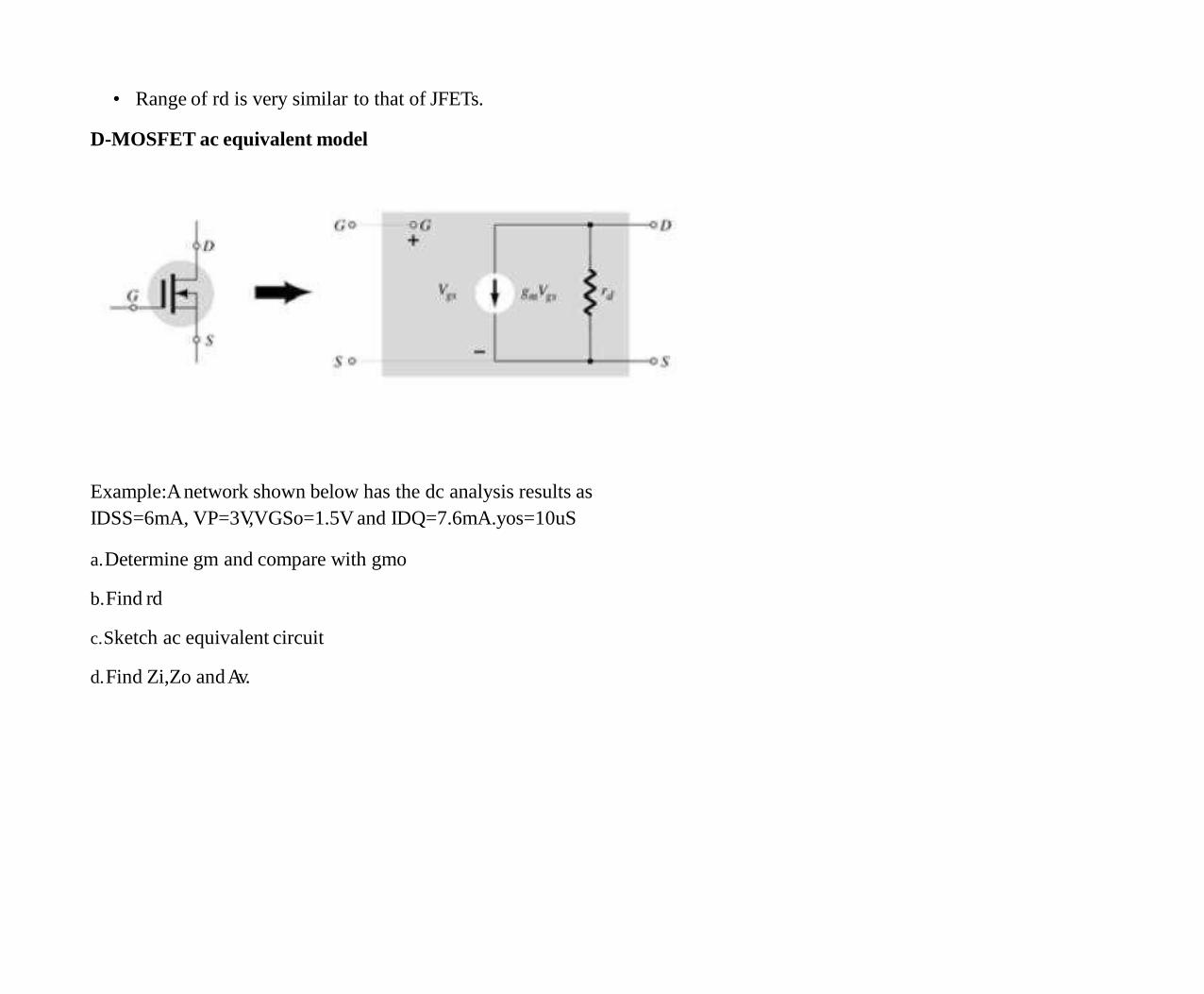
• Range of rd is very similar to that of JFETs.
D-MOSFET ac equivalent model
Example:A network shown below has the dc analysis results as
IDSS=6mA, VP=3V,VGSo=1.5V and IDQ=7.6mA.yos=10uS
a.Determine gm and compare with gmo
b.Find rd
c.Sketch ac equivalent circuit
d.Find Zi,Zo and Av.
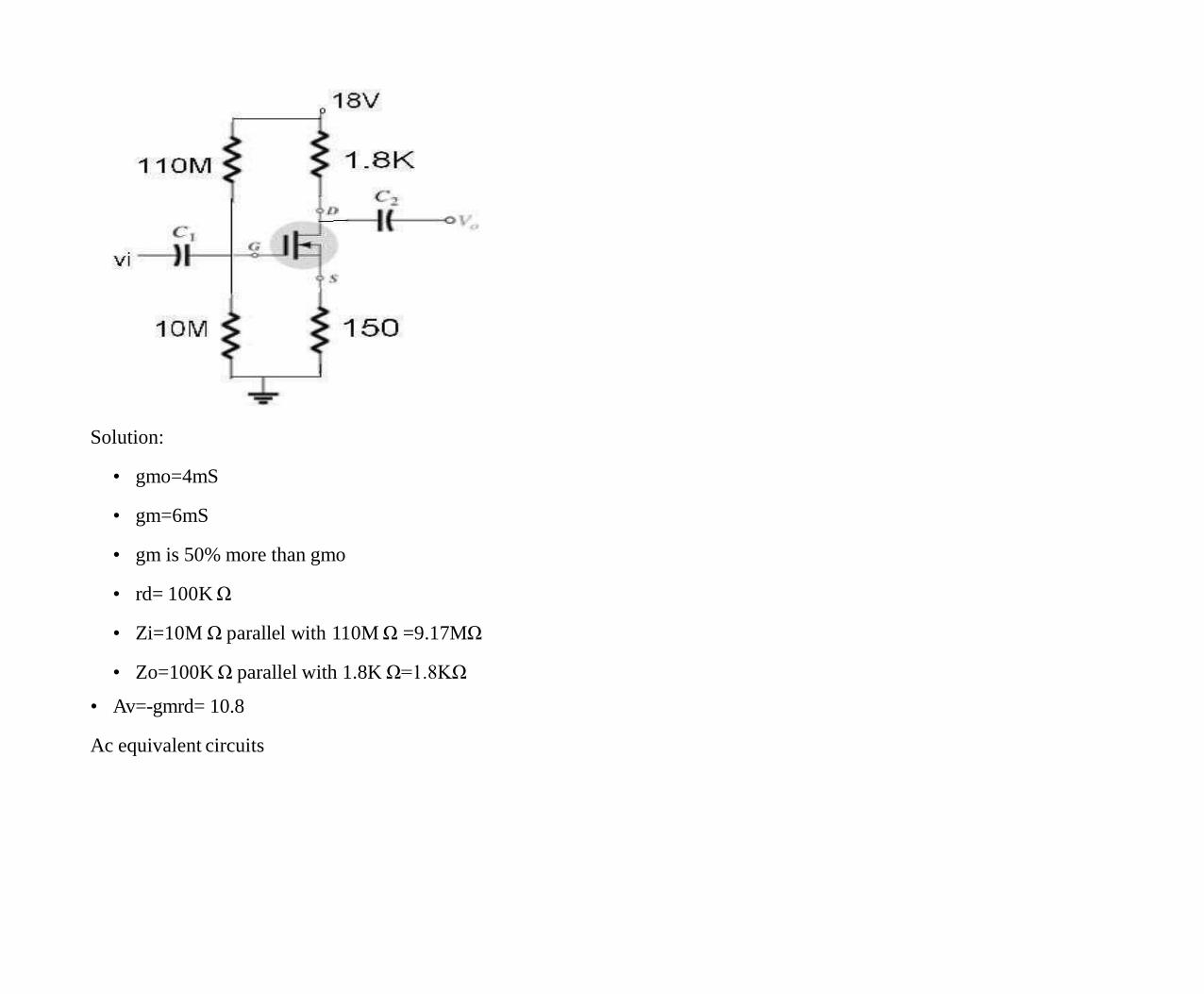
Solution:
• gmo=4mS
• gm=6mS
• gm is 50% more than gmo
• rd= 100K Ω
• Zi=10M Ω parallel with 110M Ω =9.17MΩ
• Zo=100K Ω parallel with 1.8K Ω=1.8KΩ
• Av=-gmrd= 10.8
Ac equivalent circuits

Enhancement type MOSFET
• There are two types of E-
MOSFETs: nMOS or n-channel
MOSFETs pMOS or p-channel
MOSFETs
E-M OSFET ac small signal model
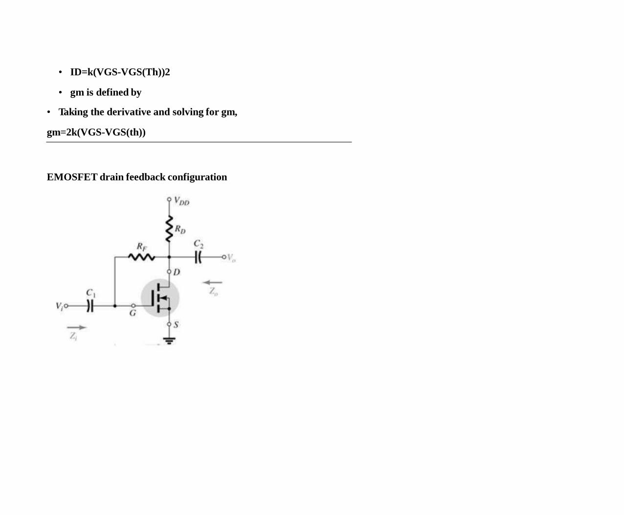
• ID=k(VGS-VGS(Th))2
• gm is defined by
• Taking the derivative and solving for gm,
gm=2k(VGS-VGS(th))
EMOSFET drain feedback configuration

Ac equivalent model
Input and output impedances
Voltage gain
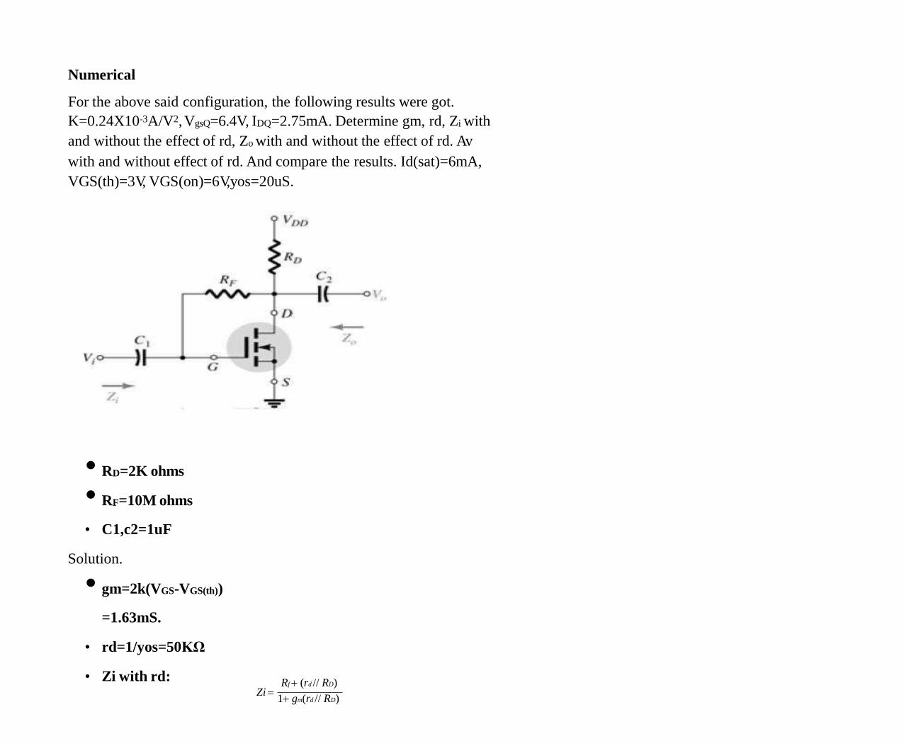
Numerical
For the above said configuration, the following results were got.
K=0.24X10⁻³A/V2, VgsQ=6.4V, IDQ=2.75mA. Determine gm, rd, Zi with
and without the effect of rd, Zo with and without the effect of rd. Av
with and without effect of rd. And compare the results. Id(sat)=6mA,
VGS(th)=3V, VGS(on)=6V,yos=20uS.
• RD=2K ohms
• RF=10M ohms
• C1,c2=1uF
Solution.
• gm=2k(VGS-VGS(th))
=1.63mS.
• rd=1/yos=50KΩ
• Zi with rd: Zi
1 gm(rd // RD)
Rf (rd // RD)
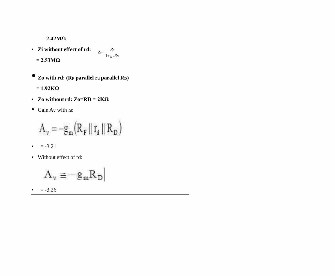
= 2.42MΩ
• Zi without effect of rd:
= 2.53MΩ
Zi RF
1 gmRD
• Zo with rd: (RF parallel rd parallel RD)
= 1.92KΩ
• Zo without rd: Zo=RD = 2KΩ
• Gain AV with rd:
• = -3.21
• Without effect of rd:
• = -3.26
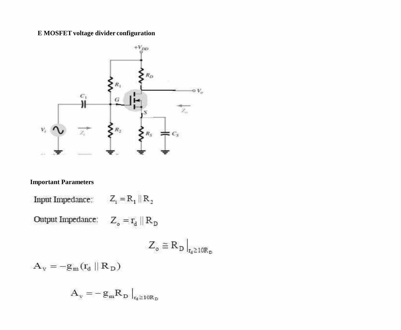
E MOSFET voltage divider configuration
Important Parameters
Ac equivalent circuit