OBE for FET Colleges management level 2 lecturer's guide ...
Upload
khangminh22Category
view
0download
0
Instruction Manual
P6205FET Probe
070-8202-01
WarningThe servicing instructions are for use by qualifiedpersonnel only. To avoid personal injury, do notperform any servicing unless you are qualified todo so. Refer to all safety summaries prior toperforming service.

Copyright � Tektronix, Inc. All rights reserved.
Tektronix products are covered by U.S. and foreign patents, issued andpending. Information in this publication supercedes that in all previouslypublished material. Specifications and price change privileges reserved.
Printed in the U.S.A.
Tektronix, Inc., P.O. Box 1000, Wilsonville, OR 97070–1000
TEKTRONIX, TEK, and TEKPROBE are registered trademarksof Tektronix, Inc.
KLIPCHIP is a trademark of Tektronix, Inc.

WARRANTY
Tektronix warrants that the products that it manufactures and sells will be free from defectsin materials and workmanship for a period of one (1) year from the date of purchase froman authorized Tektronix distributor. If any such product proves defective during thiswarranty period, Tektronix, at its option, either will repair the defective product withoutcharge for parts and labor, or will provide a replacement in exchange for the defectiveproduct. Batteries are excluded from this warranty.
In order to obtain service under this warranty, Customer must notify Tektronix of the defectbefore the expiration of the warranty period and make suitable arrangements for theperformance of service. Customer shall be responsible for packaging and shipping thedefective product to the service center designated by Tektronix, shipping charges prepaid,and with a copy of customer proof of purchase. Tektronix shall pay for the return of theproduct to Customer if the shipment is to a location within the country in which theTektronix service center is located. Customer shall be responsible for paying all shippingcharges, duties, taxes, and any other charges for products returned to any other locations.
This warranty shall not apply to any defect, failure or damage caused by improper use orimproper or inadequate maintenance and care. Tektronix shall not be obligated to furnishservice under this warranty a) to repair damage resulting from attempts by personnel otherthan Tektronix representatives to install, repair or service the product; b) to repair damageresulting from improper use or connection to incompatible equipment; c) to repair anydamage or malfunction caused by the use of non-Tektronix supplies; or d) to service aproduct that has been modified or integrated with other products when the effect of suchmodification or integration increases the time or difficulty of servicing the product.
THIS WARRANTY IS GIVEN BY TEKTRONIX WITH RESPECT TO THELISTED PRODUCTS IN LIEU OF ANY OTHER WARRANTIES, EXPRESS ORIMPLIED. TEKTRONIX AND ITS VENDORS DISCLAIM ANY IMPLIEDWARRANTIES OF MERCHANTABILITY OR FITNESS FOR A PARTICULARPURPOSE. TEKTRONIX’ RESPONSIBILITY TO REPAIR OR REPLACEDEFECTIVE PRODUCTS IS THE SOLE AND EXCLUSIVE REMEDYPROVIDED TO THE CUSTOMER FOR BREACH OF THIS WARRANTY.TEKTRONIX AND ITS VENDORS WILL NOT BE LIABLE FOR ANYINDIRECT, SPECIAL, INCIDENTAL, OR CONSEQUENTIAL DAMAGESIRRESPECTIVE OF WHETHER TEKTRONIX OR THE VENDOR HASADVANCE NOTICE OF THE POSSIBILITY OF SUCH DAMAGES.


P6205 Instruction Manual i
Table of Contents
General Safety Summary v. . . . . . . . . . . . . . . . . . . . . . . . . . . .
Service Safety Summary vii. . . . . . . . . . . . . . . . . . . . . . . . . . . . .
Preface ix. . . . . . . . . . . . . . . . . . . . . . . . . . . . . . . . . . . . . . . . . . . . Contacting Tektronix x. . . . . . . . . . . . . . . . . . . . . . . . . . . . . . . . .
Getting StartedProduct Description 1–1. . . . . . . . . . . . . . . . . . . . . . . . . . . . . . . . . .
Oscilloscopes without the TEKPROBE Interface 1–1. . . . . . . . Standard Accessories 1–3. . . . . . . . . . . . . . . . . . . . . . . . . . . . . . . . . Probe Features 1–3. . . . . . . . . . . . . . . . . . . . . . . . . . . . . . . . . . . . . . Grounding the Probe 1–7. . . . . . . . . . . . . . . . . . . . . . . . . . . . . . . . .
Operating BasicsGround Lead Inductance 2–1. . . . . . . . . . . . . . . . . . . . . . . . . . . . . . Linear Operating Range 2–3. . . . . . . . . . . . . . . . . . . . . . . . . . . . . . . High-Amplitude Frequency Response 2–3. . . . . . . . . . . . . . . . . . . .
Step Inputs 2–3. . . . . . . . . . . . . . . . . . . . . . . . . . . . . . . . . . . . . . Sine Wave Inputs 2–5. . . . . . . . . . . . . . . . . . . . . . . . . . . . . . . . .
SpecificationsPerformance Verification
Test Equipment 4–1. . . . . . . . . . . . . . . . . . . . . . . . . . . . . . . . . . . . . Attenuation Check 4–2. . . . . . . . . . . . . . . . . . . . . . . . . . . . . . . . . . . Rise Time Check 4–5. . . . . . . . . . . . . . . . . . . . . . . . . . . . . . . . . . . .
Rise Time Approximation 4–7. . . . . . . . . . . . . . . . . . . . . . . . . . Bandwidth Approximation 4–8. . . . . . . . . . . . . . . . . . . . . . . . . .
Aberrations Check 4–9. . . . . . . . . . . . . . . . . . . . . . . . . . . . . . . . . . . Output Offset Check 4–14. . . . . . . . . . . . . . . . . . . . . . . . . . . . . . . . .

Table of Contents
ii P6205 Instruction Manual
MaintenancePreventive Maintenance 5–1. . . . . . . . . . . . . . . . . . . . . . . . . . . . . . .
Visual Inspection 5–1. . . . . . . . . . . . . . . . . . . . . . . . . . . . . . . . . Cleaning 5–2. . . . . . . . . . . . . . . . . . . . . . . . . . . . . . . . . . . . . . . .
Corrective Maintenance 5–2. . . . . . . . . . . . . . . . . . . . . . . . . . . . . . . Static Sensitive Devices 5–3. . . . . . . . . . . . . . . . . . . . . . . . . . . . Replacing the Probe Tip 5–3. . . . . . . . . . . . . . . . . . . . . . . . . . . . Replacing the TEKPROBE Contact Pins 5–3. . . . . . . . . . . . . . Replacing Internal Assemblies: Probe Head and Cable,
BNC and Circuit Board Carrier 5–4. . . . . . . . . . . . . . . . . . . Readjustment Following Repair 5–6. . . . . . . . . . . . . . . . . . . . .
Repackaging for Shipment 5–6. . . . . . . . . . . . . . . . . . . . . . . . . . . .
Replaceable PartsParts Ordering Information 6–1. . . . . . . . . . . . . . . . . . . . . . . . . . . .
Module Servicing 6–1. . . . . . . . . . . . . . . . . . . . . . . . . . . . . . . . . Using the Replaceable Parts List 6–2. . . . . . . . . . . . . . . . . . . . . . . .
Abbreviations 6–3. . . . . . . . . . . . . . . . . . . . . . . . . . . . . . . . . . . . Mfr. Code to Manufacturer Cross Index 6–3. . . . . . . . . . . . . . .

Table of Contents
P6205 Instruction Manual iii
List of Figures
Figure 1–1: P6205 probe with accessories 1–2. . . . . . . . . . . . . . .
Figure 1–2: Probe finger guard and hand contact area 1–7. . . .
Figure 2–1: Equivalent circuit showing added probe andground lead resistance, capacitance, and inductance 2–1. . .
Figure 2–2: Effects of ground lead inductance on waveformfidelity 2–2. . . . . . . . . . . . . . . . . . . . . . . . . . . . . . . . . . . . . . . . .
Figure 2–3: P6205 typical input vs linear operating range 2–4.
Figure 2–4: Bandwidth vs sine wave input amplitude 2–5. . . . .
Figure 3–1: Typical input impedance vs frequency 3–5. . . . . . .
Figure 3–2: Voltage derating vs frequency 3–5. . . . . . . . . . . . . .
Figure 3–3: Linearity error vs output voltage 3–6. . . . . . . . . . . .
Figure 3–4: Typical frequency response 3–6. . . . . . . . . . . . . . . .
Figure 4–1: Attenuation test setup part 1 4–3. . . . . . . . . . . . . . .
Figure 4–2: Calibrator waveform 4–4. . . . . . . . . . . . . . . . . . . . .
Figure 4–3: Cursors placement for D voltage measurement 4–4
Figure 4–4: Attenuation test setup part 2 4–5. . . . . . . . . . . . . . .
Figure 4–5: Rise time test setup 4–6. . . . . . . . . . . . . . . . . . . . . . .
Figure 4–6: Rise time waveform 4–7. . . . . . . . . . . . . . . . . . . . . . .
Figure 4–7: Aberrations test setup part 1 4–9. . . . . . . . . . . . . . .
Figure 4–8: Aberrations waveform 4–10. . . . . . . . . . . . . . . . . . . .
Figure 4–9: Measuring aberrations 4–11. . . . . . . . . . . . . . . . . . . .
Figure 4–10: Aberrations test setup part 2 4–12. . . . . . . . . . . . . .
Figure 5–1: Disassembling the P6205 probe 5–5. . . . . . . . . . . . .
Figure 6–1: P6205 probe with standard accessories 6–4. . . . . . .
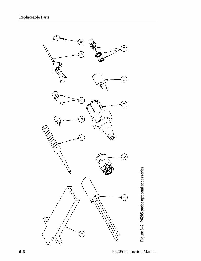
Figure 6–2: P6205 probe optional accessories 6–6. . . . . . . . . . . .

Table of Contents
iv P6205 Instruction Manual
List of Tables
Table 1–1: Standard accessories 1–3. . . . . . . . . . . . . . . . . . . . . .
Table 3–1: Electrical characteristics 3–1. . . . . . . . . . . . . . . . . . .
Table 3–2: Environmental characteristics 3–4. . . . . . . . . . . . . .
Table 3–3: Physical characteristics 3–4. . . . . . . . . . . . . . . . . . . .
Table 3–4: Certifications and compliances 3–4. . . . . . . . . . . . . .
Table 4–1: Test equipment 4–2. . . . . . . . . . . . . . . . . . . . . . . . . . .

P6205 Instruction Manual v
General Safety Summary
Review the following safety precautions to avoid injury and preventdamage to this product or any products connected to it. To avoidpotential hazards, use this product only as specified.
Only qualified personnel should perform service procedures.
While using this product, you may need to access other parts of thesystem. Read the General Safety Summary in other system manualsfor warnings and cautions related to operating the system.
To Avoid Fire or Personal InjuryConnect and Disconnect Properly. Do not connect or disconnect probesor test leads while they are connected to a voltage source.
Observe All Terminal Ratings. To avoid fire or shock hazard, observe allratings and markings on the product. Consult the product manual forfurther ratings information before making connections to the product.
Do not apply a potential to any terminal, including the commonterminal, that exceeds the maximum rating of that terminal.
Connect the ground lead of the probe to earth ground only.
Avoid Exposed Circuitry. Do not touch exposed connections andcomponents when power is present.
Do Not Operate With Suspected Failures. If you suspect there is damageto this product, have it inspected by qualified service personnel.
Do Not Operate in Wet/Damp Conditions.
Do Not Operate in an Explosive Atmosphere.
Keep Product Surfaces Clean and Dry.

General Safety Summary
vi P6205 Instruction Manual
Safety Terms and SymbolsTerms in This Manual. These terms may appear in this manual:
WARNING. Warning statements identify conditions or practices thatcould result in injury or loss of life.
CAUTION. Caution statements identify conditions or practices thatcould result in damage to this product or other property.
Terms on the Product. These terms may appear on the product:
DANGER indicates an injury hazard immediately accessible as youread the marking.
WARNING indicates an injury hazard not immediately accessible asyou read the marking.
CAUTION indicates a hazard to property including the product.
Symbols on the Product. These symbols may appear on the product:
Protective Ground(Earth) Terminal
CAUTIONRefer to Manual
DoubleInsulated
WARNINGHigh Voltage
P6205 Instruction Manual vii
Service Safety Summary
Only qualified personnel should perform service procedures. Readthis Service Safety Summary and the General Safety Summary beforeperforming any service procedures.
Do Not Service Alone. Do not perform internal service or adjustmentsof this product unless another person capable of rendering first aidand resuscitation is present.
Disconnect Power. To avoid electric shock, disconnect the mainspower by means of the power cord or, if provided, the power switch.
Use Care When Servicing with Power On. Dangerous voltages or currentsmay exist in this product. Disconnect power, remove battery (ifapplicable), and disconnect test leads before removing protectivepanels, soldering, or replacing components.
To avoid electric shock, do not touch exposed connections.

Service Safety Summary
viii P6205 Instruction Manual

P6205 Instruction Manual ix
Preface
This manual provides operating and maintenance information for theTektronix P6205 FET probe.
The manual is organized into the following sections:
� Getting Started provides a product overview and introduction toprobe features and accessories.
� Operating Basics discusses techniques for improving measure-ment accuracy.
� Specifications lists the probe warranted characteristics.
� Performance Verification contains procedures to verify probeperformance.
� Maintenance contains inspection and cleaning procedures andinstructions for replacing probe modules.
� Replaceable Parts lists the standard and optional probe parts andaccessories and provides ordering information.

Preface
x P6205 Instruction Manual
Contacting Tektronix
ProductSupport
For application-oriented questions about a Tektronixmeasurement product, call toll free in NorthAmerica:1-800-TEK-WIDE (1-800-835-9433 ext. 2400)6:00 a.m. – 5:00 p.m. Pacific time
Or contact us by e-mail:[email protected]
For product support outside of North America,contact your local Tektronix distributor or salesoffice.
ServiceSupport
Contact your local Tektronix distributor or salesoffice. Or visit our web site for a listing ofworldwide service locations.
http://www.tek.com
For otherinformation
In North America:1-800-TEK-WIDE (1-800-835-9433)An operator will direct your call.
To write us Tektronix, Inc.P.O. Box 1000Wilsonville, OR 97070-1000

Getting Started


P6205 Instruction Manual 1–1
Getting Started
The Tektronix P6205 FET probe is an active 10X-attenuating probethat is compatible with Tektronix TDS 500 Series, DSA 600 Series,11000 Series, and CSA 404 oscilloscopes and plug-in units.
Product DescriptionThe P6205 probe provides high-frequency measurement capabilitywithout the capacitive loading and performance limitations inherentin passive resistive-divider type probes. FETs are used in the P6205to establish the characteristic high input impedance at highfrequency of an active probe. The P6205 features a 750 MHzbandwidth with an input impedance of 1 M� in parallel with 2 pF.You must terminate the P6205 probe output into 50 �.
The P6205 includes the TEKPROBE� Level 2 interface. When usedwith a fully TEKPROBE interface-compatible oscilloscope, theP6205 probe is powered by the host instrument and provides theoscilloscope with the probe model number, serial number, andattenuation factor. When installed on a fully compatible oscillo-scope, the oscilloscope channel input is automatically set to 50 �
and the display readouts are corrected for the probe attenuationfactor.
Oscilloscopes without the TEKPROBE Interface
The P6205 is an active probe that requires external power to operate.If your oscilloscope is not equipped with the TEKPROBE interface,we recommend that you use the Tektronix 1103 TEKPROBE PowerSupply. By connecting the probe to the 1103 power supply, and thepower supply output to your oscilloscope input, you can use theP6205 probe with oscilloscopes having conventional BNC inputs.The 1103 can power two P6205 probes simultaneously.
To maintain the best possible high-frequency response with the 1103power supply, keep the cable connecting the 1103 output to theoscilloscope input as short as possible. You must use an oscilloscopewith 50 � input impedance with this system.
Getting Started
1–2 P6205 Instruction Manual
NOTE. Using the P6205 probe with an 1103 power supply will notadd full TEKPROBE functionality to an incompatible oscilloscope.In addition, the 1103 probe offset adjustment does not apply toP6205 probes.
1
2
3
4
5
6
7
8
9
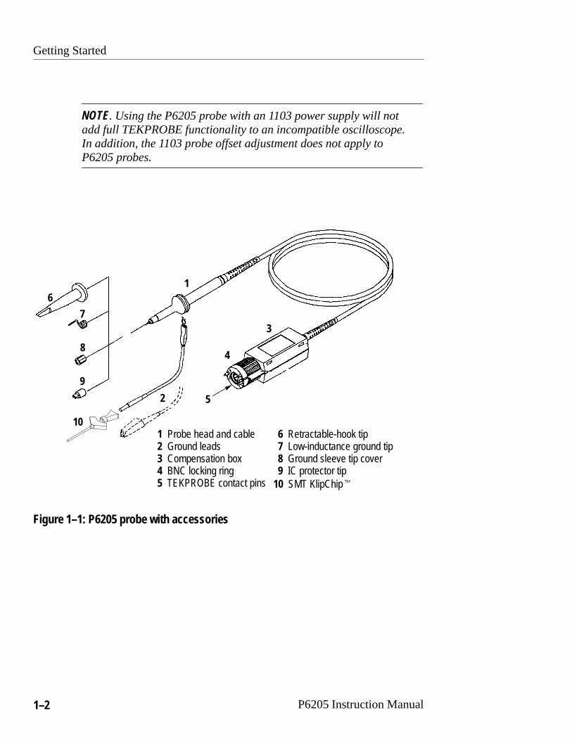
101 Probe head and cable2 Ground leads3 Compensation box4 BNC locking ring5 TEKPROBE contact pins
6 Retractable-hook tip7 Low-inductance ground tip8 Ground sleeve tip cover9 IC protector tip
10 SMT KlipChip�
Figure 1–1: P6205 probe with accessories
Getting Started
P6205 Instruction Manual 1–3
Standard AccessoriesTable 1–1 lists the P6205 probe standard accessories.
Table 1–1: Standard accessories
1 Retractable-hook tip
1 Ground lead with square-pin receptacle
1 Ground lead with alligator clip
1 Ground contact spring
1 Ground sleeve tip cover
1 IC protector tip
1 SMT KlipChip
1 Instruction manual
The Replaceable Parts section beginning on page 6–1, containsordering information for all standard and optional accessories.
Probe FeaturesThe following table introduces P6205 probe components, connectors,and accessories. Refer to Figure 1–1 to identify probe items andwhere to attach standard accessories.
Probe Head and Cable. The probe tip makes a physicalconnection to the test point. The flexible cable allows you to makemeasurements in a variety of applications.
Compensation Box. The compensation box contains circuitry,including elements of the TEKPROBE interface. There are nointernal adjustments.

Getting Started
1–4 P6205 Instruction Manual
Data
–5 V
+5 V
ClockSignalGround
TEKPROBE Interface (Level 2). The TEKPROBE interfaceprovides a communication path between the probe and the hostinstrument. Contact pins provide connections for power, signal,and data transfer. The interface allows some oscilloscopes toautomatically configure the correct attenuation factor and inputimpedance and to access the probe serial number.
Some features of the TEKPROBE interface, for example probeoffset and additional voltage sources, are not required by theP6205; therefore, the contact pins are omitted from the connector.
NOTE. Your oscilloscope may not implement all features ofthe TEKPROBE interface. Refer to your oscilloscopemanual for details.
BNC Locking Ring. The BNC locking ring houses theTEKPROBE interface contact pins and provides a positiveattachment to the host instrument.
To install the probe, open the locking ring by rotating itcounterclockwise; push the assembly firmly onto the oscilloscope(or power supply) BNC input connector. Rotate the ring clockwiseone-quarter turn to secure it to the input connector.
Retractable-Hook Tip.1 Attach the retractable-hook tip to yoursignal test point for hands-free operation. The hook tip attacheseasily to leaded components such as resistors, capacitors, anddiscrete semiconductors. Stripped wire, jumpers, busses, and testpins can also be gripped with the retractable hook tip.
To remove the hook tip (your probe is shipped with the hook tipinstalled), simply pull it off. Reinstall the hook tip by pushing itfirmly onto the molded barrel of the probe tip.
IC Protector Tip.2 Use the IC protector tip to simplify probing ofin-line IC packages. The shape of the protector tip guides theprobe onto IC pins and prevents accidental shorting of pins by theprobe tip.
To install the IC protector tip, push it firmly onto the end of themetal barrel of the probe tip while taking care not to pierceyourself with the sharp tip.
NOTE: Remove the IC protector tip by pulling it off beforeinstalling the retractable-hook tip.

Getting Started
P6205 Instruction Manual 1–5
Ground Sleeve Tip Cover.2 Use the ground sleeve tip cover tokeep the metal sleeve of the probe tip from accidentally shortingcomponents on your device under test.
To install the ground sleeve tip cover, push it onto the metal barrelof the probe tip while taking care not to pierce yourself with thesharp probe tip. Remove the sleeve by pulling it off beforeinstalling the retractable hook tip.
Ground Leads.1 Use the long ground leads when length isimportant and precise high-frequency measurement is not. Longground leads are ideal for quick troubleshooting when you arelooking for the presence, absence, or general shape of a signal.For maximum performance, always use the shortest ground leadpossible.
To attach the ground lead, press the spring clip onto the collar ofthe probe head. An alternative ground connection can also bemade to the metal barrel of the probe tip.
Low-Inductance Ground Contact (Spring Tip). Use thelow-inductance spring-tip ground contact to reduce ground leadinductance. The performance of a probe fitted with thelow-inductance ground contact approaches that of no-lead probefixtures and adapters. With the spring-tip contact installed, youcan make measurements up to the system bandwidth of yourprobe/oscilloscope with negligible signal degradation from groundlead inductance.
To install the low-inductance ground contact, push it onto themetal barrel of the probe tip while taking care not to pierceyourself with the sharp probe tip.
NOTE: The spring contact installs more easily if you rotatethe spring counterclockwise (loosening the spring tension)as you push it onto the probe barrel. Use care to avoid theaccidentally shorting of component leads to ground whenusing this tip.

Getting Started
1–6 P6205 Instruction Manual
SMT KlipChip�. Use the retractable KlipChip if you needhands-free attachment to a physically small signal or groundsource. The low profile of the KlipChip allows you to graspdevices that the Retractable Hook Tip cannot.
To use the KlipChip as a ground connector, attach the longground lead with square-pin termination to the probe collar.Connect the ground lead termination to one of the KlipChipshoulder pins.
To use the KlipChip as a signal connector, slide the optionalsingle-lead probe tip adapter (see Replaceable Parts list) onto theprobe tip. Connect the single-lead termination to one of theKlipChip shoulder pins.
To use the KlipChip as both ground and signal connector, slidethe optional dual-lead probe tip adapter (See Replaceable Parts)onto the probe tip. Connect both single-lead terminations to theshoulder of a separate KlipChip pin. You can also combine thesingle-lead adapter with a long ground lead to configure dualKlipChip connections.
1 For maximum flexibility, use one of the six-inch ground leads. For precisemeasurements at high frequency, the inductance associated with long groundleads may distort the high-frequency component of your signal. Considerwhether you can use one of the low-inductance probe tip configurationsinstead. For tips on minimizing ground lead inductance, refer to the OperatingBasics section beginning on page 2–1.
2 Use a ground lead with this accessory. Be sure to take into account groundlead inductance effects on measurements at frequencies approaching 30 MHz.For tips on minimizing ground lead inductance, refer to the Operating Basicssection beginning on page 2–1.

Getting Started
P6205 Instruction Manual 1–7
Grounding the ProbeConnect the probe to the instrument and connect the ground lead toground before making any measurements. Ensure that no part of theground lead contacts voltage in the circuit under test. Except for theprobe tip and BNC center conductor, all accessible metal (includingthe ground clip) is connected to the BNC shell.
WARNING. To avoid electric shock when using the probe, keep yourfingers behind the finger guard on the probe body. See Figure 1–2below.
Hand contact area
Fingerguard
Figure 1–2: Probe finger guard and hand contact area

Getting Started
1–8 P6205 Instruction Manual

Operating Basics


P6205 Instruction Manual 2–1
Operating Basics
This section discusses technical issues you should consider whenusing the P6205 probe.
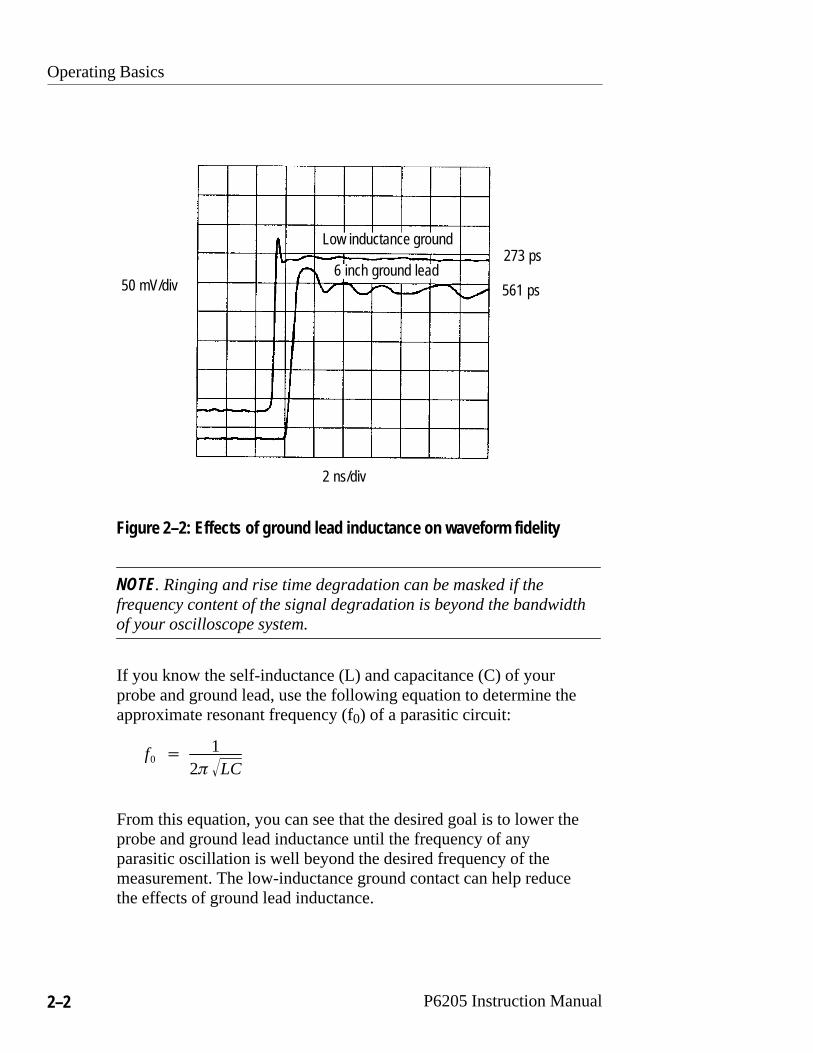
Ground Lead InductanceWhen you touch the probe tip to a circuit element you are introduc-ing a new resistance, capacitance, and inductance into the circuit.See Figure 2–1.
Rsource
Rin 1 M�
Lgl Ground lead
VSourceProbeCin = 2 pF
Probe
Figure 2–1: Equivalent circuit showing added probe and ground leadresistance, capacitance, and inductance
The high input resistance of the P6205 probe has negligible effect onmost circuits. The series inductance introduced by the probe tip andground lead however, can result in a parasitic resonant circuit that“rings” within the bandwidth of your oscilloscope system. Fig-ure 2–2 shows examples of how different ground leads affect adisplayed signal.
Operating Basics
2–2 P6205 Instruction Manual
273 ps
561 ps
Low inductance ground
6 inch ground lead
2 ns/div
50 mV/div
Figure 2–2: Effects of ground lead inductance on waveform fidelity
NOTE. Ringing and rise time degradation can be masked if thefrequency content of the signal degradation is beyond the bandwidthof your oscilloscope system.
If you know the self-inductance (L) and capacitance (C) of yourprobe and ground lead, use the following equation to determine theapproximate resonant frequency (f0) of a parasitic circuit:
f0 �1
2� LC�
From this equation, you can see that the desired goal is to lower theprobe and ground lead inductance until the frequency of anyparasitic oscillation is well beyond the desired frequency of themeasurement. The low-inductance ground contact can help reducethe effects of ground lead inductance.

Operating Basics
P6205 Instruction Manual 2–3
Linear Operating RangeThe internal probe amplifier has a finite operating range whenterminated into a 50 � load. To maintain a linearity error below 4%,limit the input signal amplitude to ±10 V. Refer to Figure 3–3 onpage 3–6 for data on linear operating range.
NOTE. The P6205 probe can sustain input voltages to ±40 V withoutdamage; however, the linearity error specification does not apply toinput voltages exceeding ±10 V.
High-Amplitude Frequency ResponseInput signal amplitude also affects probe frequency response. Figures2–3 and 2–4 characterize the effects of probe frequency response interms of rise time for step inputs and –3 dB bandwidth for sine waveinputs.
Step Inputs
Degradation of high-amplitude step inputs generally appear asslower rise times and distorted responses. Figure 2–3 shows probelinear operating range as a function of input step voltage, in terms ofrise time and fall time.

Operating Basics
2–4 P6205 Instruction Manual
0 2.5 V 5 V 7.5 V 10 V
2
1
.5
Input step (Vp–p step)
Inpu
t sig
nal r
ise
time
(ns)
Inpu
t sig
nal f
all t
ime
(ns)
Accurate measuring area
Nonlinear area
1.5
0 2.5 V 5 V 7.5 V 10 V
2
Input step (Vp–p step)
Accurate measuring area
Nonlinear area
1
.5
1.5
Figure 2–3: P6205 typical input vs linear operating range

Operating Basics
P6205 Instruction Manual 2–5
Sine Wave Inputs
Degradation of high-amplitude sine wave inputs generally appear asharmonic distortion and reduced peak-to-peak amplitude. Figure 2–4shows the –3 dB bandwidth of sine wave inputs as a function ofamplitude.
0 2 4 6 8 10
800
600
400
200
Amplitude (Vp–p sinewave)
–3 d
B fre
quen
cy (M
Hz)
Figure 2–4: Bandwidth vs sine wave input amplitude

Operating Basics
2–6 P6205 Instruction Manual

Specifications


P6205 Instruction Manual 3–1
Specifications
This section lists the electrical, environmental, and physicalspecifications of the P6205 probe. All specifications are guaranteedunless labeled “typical”. Typical specifications are provided for yourconvenience and are not guaranteed. Specifications marked with the� symbol are verified in in the Performance Verification sectionbeginning on page 4–1.
The electrical characteristics listed in Table 3–1 apply to a probecalibrated between 20� C and 30� C. The instrument system mustalso be calibrated and operating within the environmental conditionslisted in Table 3–2 on page 3–4.
Following the specification tables you will find a series of graphsshowing typical probe characteristics.
Table 3–1: Electrical characteristics
Characteristic Description
�Attenuation1 10X ±1.8% at DC into 50 � ±0.5% load
Input resistance2,3 1 M� ±5% at DC
Input capacitance ≤2 pF
�Rise time3 < 467 ps
Bandwidth3 Derived from rise time (BW = 0.35/tr): 750 MHz

Specifications
3–2 P6205 Instruction Manual
Table 3–1: Electrical characteristics (Cont.)
Characteristic Description
Bandwidth, typical
Mainframe:
TDS500/600TDS40011402A/11403A
450 MHz325 MHzSee plug-in unit
Plug-in unit:
11A3211A3311A34V11A5211A72
350 MHz125 MHz275 MHz475 MHz600 MHz
�Aberrations3,4
first 20 ns ±7%, 10% peak to peak
20 ns to 2 �s ±3%, 5% peak to peak
Propagation delay Probe tip to output connector measured atwaveform 50% points: 6.72 ns ±200 ps
�Output offset3,5 At 25� C (77� F): less than ±10 mV
±100 mV on screen for oscilloscopes thatrecognize probe coding
Linearity6
Linear input range ±10 V
Linearity error Relative to full-scale output with ±10 V input:< 4%
DC Thermal drift3,7 Less than ±100 mV/�C
For scopes that recognize probe coding: ±1 mVon screen
Output load requirement 50 � ±0.5%
Maximum nondestructive input voltage 40 VDC + peak AC

Specifications
P6205 Instruction Manual 3–3
Table 3–1: Electrical characteristics (Cont.)
Characteristic Description
Electrostatic immunity Sustains discharge from a 500 pF capacitorcharged to 10 kV, through a 1 k� resistance tothe probe tip or a TEKPROBE connector pin.
Power supply requirements8
+5 V supply +5 V ±2%, 110 mA maximum
–5 V supply –5 V ±2%, 50 mA maximum
Power consumption Host instrument input power: 1.25 W maximum1 11000 Series mainframes: use the probe calibrate function to gain additional
accuracy.2 With probe operating.3 Probe only.4 When used with a system having a rise time of less than 100 ps, refer to
Aberrations in the Performance Verification section.5 11000 Series oscilloscopes only: less than 2 mV following oscilloscope
calibration.6 See page 2–4: Linear Operating Range.7 At probe output.8 Less accurate supply levels increase output offset error.

Specifications
3–4 P6205 Instruction Manual
Table 3–2: Environmental characteristics
Characteristic Description
Temperature range
Operating 0� C to +50� C(32� F to 122� F)
Nonoperating –55� C to +75� C(–67� F to 167� F)
Humidity Five cycles (120 hr) at 90 to 95% relativehumidity
Altitude
Operating To 4,600 m (15,000 ft)
Transportation Qualifies under National Safe Transit Associa-tion Preshipment Procedure 1–A–B–1
Table 3–3: Physical characteristics
Characteristic Description
Shipping weight1 0.9 kg (2 lbs)
Probe cable length 1.5 m (60 in) tip to BNC
1 Includes accessories.
Table 3–4: Certifications and compliances
Pollution degree Degree 2
Safety class Class 1 (ground reference)

Specifications
P6205 Instruction Manual 3–5
Mag
nitu
de (o
hms)
Frequency
Phas
e (d
egre
es)
+50
+25
0
–25
–50
–75
–125
–100
1M
100k
10k
1k
100
1010kHz 100kHz 1MHz 10MHz 100MHz 1GHz 10GHz
ohmsdegrees
Figure 3–1: Typical input impedance vs frequency
50
40
30
20
10
0
Max
imum
inpu
t vol
tage
(V)
Frequency
100MHz10MHz 1GHz 10GHz
Figure 3–2: Voltage derating vs frequency

Specifications
3–6 P6205 Instruction Manual
VoutVin
10–
Vin
Attenuation
+15mV
+10mV
+5mV
0
–5mV
–10mV
–15mV–15/10 –10/10 –5/10 0 +5/10 +10/10 +15/10
Figure 3–3: Linearity error vs output voltage
Vout (dB)
1
0
–1
–2
–3
–4
–5
–6100kHz 1MHz 10MHz 100MHz 1GHz
Frequency
Figure 3–4: Typical frequency response

Performance Verification


P6205 Instruction Manual 4–1
Performance Verification
This section contains procedures to verify that the P6205 probemeets the performance requirements listed in the Specificationssection. The performance verification procedures consists of thefollowing checks:
� Attenuation
� Rise Time
� Aberrations
� Output offset
Performance characteristics not verified by the performanceverification procedures are either extremely stable or impractical toverify.
Use the performance verification procedures as an acceptancecriteria or to verify probe performance following repair.
Under normal operating conditions, verify the performance of yourprobe at least once a year.
Test EquipmentTable 4–1 lists the recommended test equipment used in theperformance verification procedures. The equipment recommendedis the minimum necessary to provide accurate results. Substituteequipment must meet or exceed the specifications listed.
If you are unfamiliar with the operation of the recommended testequipment, refer to the individual users manuals for instructions.
NOTE. Before beginning any performance verification procedure,warm up all test equipment for at least 20 minutes.

Performance Verification
4–2 P6205 Instruction Manual
Table 4–1: Test equipment
Description Minimum Requirement Example Product
Oscilloscope DC to 10 GHz, 50 � input Tektronix 11801B withSD-24 TDR sampling head
Probe power supply TEKPROBE interface con-nector
Tektronix 1103 TEKPROBEpower supply
Calibration generator Amplitude accuracy: ±0.25% Calibration signal from11801B oscilloscope
Pulse generator Rise time: <100 ps Calibration signal from11801B oscilloscope
Termination adapter 50 �, probe-to-GR Tektronix part number017-0088-00
Female BNC-to-GR adapter Tektronix part number017-0063-00
Male SMA-to-BNC femaleadapters (2)
Tektronix part number015-0554-00
Male SMA-to-GR adapter Tektronix part number015-1007-00
Coaxial cable 50 � BNC, 10 inch length Tektronix part number012-0208-00
Attenuation CheckUse the following procedure to confirm that the P6205 probeperforms within its Attenuation specification limits.
1. Set the oscilloscope controls as indicated in the table below.
Oscilloscope settings
Control Setting
Volts/division 50 mV
Time/division 2 �s

Performance Verification
P6205 Instruction Manual 4–3
Oscilloscope settings (Cont.)
Control Setting
Trigger source Internal clock
Trigger mode Auto
Coupling DC
Waveform averaging On
Number of waveforms to average 8
Cursor type Horizontal bars
Cursor knob resolution Fine
2. Install one SMA-to-BNC adapter on an SD-24 sampling headinput channel and another adapter on the oscilloscope calibratoroutput. Use the 10-inch coaxial cable to connect the oscilloscopecalibrator output to the SD-24 input channel. See Figure 4–1below.
11801B oscilloscope
Figure 4–1: Attenuation test setup part 1
3. Press SELECT CHANNEL on the sampling head to enable thecorresponding input channel.
4. Adjust the oscilloscope controls as necessary to display awaveform similar to the one shown in Figure 4–2 below.

Performance Verification
4–4 P6205 Instruction Manual
Figure 4–2: Calibrator waveform
5. Store and then recall the waveform.
6. Use the oscilloscope cursors to display the � voltage of therecalled waveform. Measure the low-frequency portion of thewaveform near the back corner. See figure 4–3 below.
Figure 4–3: Cursors placement for � voltage measurement
7. Record the � voltage as V1.
8. Disconnect the coaxial cable from the oscilloscope calibratoroutput and reconnect it to the channel 1 output of the 1103 probepower supply. Remove the SMA-to-BNC adapter from theoscilloscope calibrator output.
9. Connect the P6205 probe output to the 1103 power supplychannel 1 input. The P6205 does not use the offset capability ofthe 1103 power supply; the offset control setting is not important.
10.Mate the GR connector ends of the 50 � termination adapter andthe male SMA-to-GR adapter. Connect the mated assembly to theoscilloscope calibrator output. Insert the probe tip firmly into the50 � termination adapter. See Figure 4–4 below.

Performance Verification
P6205 Instruction Manual 4–5
1103 power supply11801Boscilloscope
Figure 4–4: Attenuation test setup part 2
11.Adjust the oscilloscope vertical position control if necessary tocenter the resulting waveform. Store and then recall thewaveform.
12.Use the cursor measurement capability of the oscilloscope todisplay the � voltage of the recalled waveform. Measure thelow-frequency portion of the waveform near the back corner.Record the � voltage as V2.
13.Use the following equation to calculate the attenuation error:
%error �V2(10) – V1
V1� 100
14.Verify that the probe attenuation error is ≤1.8%.
Rise Time CheckUse the following procedure to confirm that the P6205 probeperforms within its Rise Time specification limits.
NOTE. If you do not have access to an 11800 Series oscilloscope, amethod for approximating probe rise time using a pulse generatorand a TDS 500 or 11000 Series oscilloscope follows this procedure.

Performance Verification
4–6 P6205 Instruction Manual
1. Set the oscilloscope controls as indicated in the table below.
Oscilloscope settings
Control Setting
Volts/division 5 mV
Time/division 500 ps
Trigger coupling DC
Trigger source Internal clock
Trigger mode Auto
Waveform averaging On
Number of waveforms to average 8
2. Connect one end of the 10-inch coaxial cable to the channel 1output of the 1103 probe power supply. Use a male SMA-to-BNCfemale adapter to connect the free end of the cable to an SD-24sampling head input. See Figure 4–5 below.
1103 power supply11801Boscilloscope
Figure 4–5: Rise time test setup
3. Press SELECT CHANNEL on the sampling head to enable thecorresponding input channel.
4. Connect the P6205 probe to the 1103 probe power supplychannel 1 input. The P6205 does not use the offset capability of

Performance Verification
P6205 Instruction Manual 4–7
the 1103 probe power supply; the offset control setting is notimportant.
5. Mate the GR ends of the male SMA-to-GR and 50 � terminationadapters. Connect the mated assembly to the oscilloscopecalibrator output. Insert the P6205 probe tip firmly into thetermination adapter. See Figure 4–5 above.
6. Adjust the oscilloscope horizontal and vertical position controlsto display a waveform similar to the one shown in Figure 4–6below.
Figure 4–6: Rise time waveform
7. Use the oscilloscope measurement capability to display andmeasure the waveform rise time (from the 10% to 90% amplitudepoints).
8. Verify that the probe rise time is equal to or less than 467 ps.
Rise Time Approximation
Use the following procedure to approximate the probe rise timewithout an 11801B oscilloscope. The procedure requires a pulsegenerator capable of producing a rise time step of 250 ps or less.
1. Use a 50 � coaxial cable to connect the output of the pulsegenerator directly to the oscilloscope input.
2. Set the time base to 1 ns/division and the vertical amplifier to50 mV/division. Adjust the pulse for a duration of greater than10 ns with an amplitude of 250 mV.
3. Save and then recall the waveform.
Performance Verification
4–8 P6205 Instruction Manual
4. Measure and record as system rise time (trs), the rise time of thedisplayed pulse.
5. Mate the 50 � termination adapter to the female BNC-to-GRadapter. Disconnect the coaxial cable at the oscilloscope andattach the mated adapters to the coaxial cable. Connect the P6205probe to the same oscilloscope input and insert the probe tipfirmly into the termination adapter.
6. Save and then recall the waveform.
7. Adjust the oscilloscope controls to display this waveform at thesame vertical scale as the first waveform. Measure and record asprobe-plus-system rise time (trp+s), the rise time of the displayedpulse.
8. Calculate the probe rise time (trp) using the equation below.Accuracy of the approximation is limited by oscilloscope systemperformance.
trp � t 2rp�s
– t 2rs
�
The calculated probe rise time should be less than 467 ps. If the risetime value exceeds this limit, use the procedure beginning onpage 4–5 to more accurately determine the probe rise time.
Bandwidth Approximation
You can calculate the approximate bandwidth from the rise timemeasurement with the following equation:
BW � .35tr
NOTE. This calculation does not constitute a valid performanceverification criteria.

Performance Verification
P6205 Instruction Manual 4–9
Aberrations CheckUse the following procedure to confirm that the P6205 probeperforms within its Aberrations specifications limits.
1. Set the oscilloscope controls as indicated in the table below.
Oscilloscope settings
Control Setting
Volts/division 50 mV
Time/division 500 ps
Trigger coupling DC
Trigger source Internal clock
Trigger mode Auto
Waveform averaging On
Number of waveforms to average 8
2. Install one SMA-to-BNC adapter on an SD-24 sampling headinput channel and another adapter on the oscilloscope calibratoroutput. Use the 10-inch coaxial cable to connect the oscilloscopecalibrator output to the SD-24 input channel. See Figure 4–7below.
11801B oscilloscope
Figure 4–7: Aberrations test setup part 1

Performance Verification
4–10 P6205 Instruction Manual
3. Press SELECT CHANNEL on the sampling head to enable thecorresponding input channel.
4. Adjust the oscilloscope controls as necessary to display awaveform similar to the one shown in Figure 4–8 below.
Figure 4–8: Aberrations waveform
5. Use the oscilloscope rise time filter capability to limit thewaveform rise time to 100 ps. Use the waveform VerticalDescription menu to set the vertical description as follows:
Filter(M1,100E-12)
NOTE. The filter description above applies to an SD-24 samplinghead installed in the 11801B mainframe M1 plug-in compartment; ifyour sampling head is installed in a different compartment, select thecorresponding mainframe designator.
6. Use the oscilloscope measurement capability to determine thepeak-to-peak amplitude of the filtered pulse. Measure, calculate,and record (in percent) the system aberrations (abss) in the first4 ns of the waveform.
NOTE. Part one of the aberrations specification applies to the first20 ns of the waveform. Significant aberrations are usually complete-ly damped beyond approximately 4 ns.

Performance Verification
P6205 Instruction Manual 4–11
Measure the peak negative-going aberration (if any) and the peakpositive-going aberration (if any). The sum of the two is thepeak-to-peak aberration, in percent.
NOTE. If the waveform front corner appears rounded or rolled-off, setthe left-limit measurement cursor at the first 100% amplitude pointof the waveform to determine aberrations. Refer to Figure 4–9.
Positive aberration
100%
90%
10%
Rise time
20ns
Negative aberration
2�s
Peak-to-peak aberration
Figure 4–9: Measuring aberrations
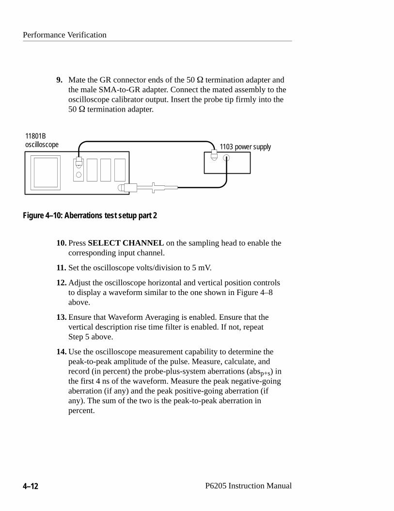
7. Disconnect the coaxial cable from the oscilloscope calibratoroutput and reconnect it to the channel 1 output of the 1103 probepower supply. Remove the SMA-to-BNC adapter from theoscilloscope calibrator output. See Figure 4–10 below.
8. Connect the P6205 probe output to the 1103 power supplychannel 1 input. The P6205 does not use the offset capability ofthe 1103 probe power supply; the offset control setting is notimportant.
Performance Verification
4–12 P6205 Instruction Manual
9. Mate the GR connector ends of the 50 � termination adapter andthe male SMA-to-GR adapter. Connect the mated assembly to theoscilloscope calibrator output. Insert the probe tip firmly into the50 � termination adapter.
1103 power supply11801Boscilloscope
Figure 4–10: Aberrations test setup part 2
10.Press SELECT CHANNEL on the sampling head to enable thecorresponding input channel.
11.Set the oscilloscope volts/division to 5 mV.
12.Adjust the oscilloscope horizontal and vertical position controlsto display a waveform similar to the one shown in Figure 4–8above.
13.Ensure that Waveform Averaging is enabled. Ensure that thevertical description rise time filter is enabled. If not, repeatStep 5 above.
14.Use the oscilloscope measurement capability to determine thepeak-to-peak amplitude of the pulse. Measure, calculate, andrecord (in percent) the probe-plus-system aberrations (absp+s) inthe first 4 ns of the waveform. Measure the peak negative-goingaberration (if any) and the peak positive-going aberration (ifany). The sum of the two is the peak-to-peak aberration inpercent.

Performance Verification
P6205 Instruction Manual 4–13
NOTE. If the waveform front corner appears rounded or rolled-off, setthe left-limit measurement cursor at the first 100% amplitude pointof the waveform. Refer to Figure 4–9 above.
15.The probe aberrations are approximately the difference betweenthe measured probe aberrations and the oscilloscope systemaberrations. Subtract the system aberrations (Step 6) from themeasured aberrations (Step 14) for both the peak and thepeak-to-peak aberrations.
absp � absp�s – abss
NOTE. In some cases the measured aberrations are less than thesystem aberrations. This situation occurs when the slower rise timeof the probe (compared to the oscilloscope/sampling head combina-tion) filters out a portion of the higher-frequency aberrations.
16.Verify that the probe-only aberrations meet specifications:
peak, first 20 ns ±7%peak to peak, first 20 ns 10%
17.Repeat steps 1 through 15 above using an oscilloscope sweepspeed of 500 ns per division. Adjust the oscilloscope as necessaryto display one pulse step and at least 2 �s of settling time.
Optional: Increasing the number of waveforms averaged willreduce the effects of noise on the smaller aberrations in the latterpart of the signal.
18.Verify that the probe-only aberrations meet specifications:
peak, 20 ns to 2 �s ±3%peak to peak, 20 ns to 2 �s 5%

Performance Verification
4–14 P6205 Instruction Manual
Output Offset CheckUse the following procedure to confirm that the P6205 probeperforms within its Output Offset specification limits.
1. Set the oscilloscope controls as indicated in the table below.
Oscilloscope settings
Control Setting
Volts/division 2 mV
Trigger coupling DC
Time/division 1 ps
Trigger mode Auto
Enhanced accuracy On
2. Install an SMA-to-BNC adapter on one of the SD-24 samplinghead inputs. Use a 10-inch coaxial cable to connect the output ofthe 1103 probe power supply to an SD-24 input channel.
3. Press SELECT CHANNEL on the sampling head to enable thecorresponding input channel.
4. Adjust the oscilloscope offset or position control to center thetrace at 0 V (or less than 1 mV).
Optional method: Use the oscilloscope measurement capability todisplay the mean voltage of the free-running trace.
5. Insert the P6205 probe tip firmly into the 50 � terminationadapter. (The BNC end remains unused.)
6. Connect the probe output to the 1103 probe power supply input.
7. Verify that the probe output offset (displacement of thefree-running trace) is less than ±10 mV.

Maintenance


P6205 Instruction Manual 5–1
Maintenance
The Maintenance section provides information on the followingtopics:
� Inspecting and cleaning the probe
� Replacing the probe tip
� Replacing TEKPROBE contact pins
� Replacing internal modules
� Packaging the probe for shipment
Preventive MaintenancePreventive maintenance consists of visually inspecting and cleaningthe probe. Perform preventive maintenance on a regular basis toprevent breakdown and improve reliability. The frequency ofmaintenance depends on the environmental operating conditions. Agood time to perform maintenance is just before a performanceverification or calibration.
WARNING. To prevent electric shock, disconnect the probe from thesignal source and oscilloscope or power supply before performingpreventive maintenance.
Visual Inspection
The best indicator of probe condition is performance. In addition toperforming the performance verification procedures, occasionallyinspect the probe tip, body, cable, compensation box, and BNCconnector for bent, broken, or damaged parts. To ensure optimumperformance, replace damaged assemblies as soon as practical.
Maintenance
5–2 P6205 Instruction Manual
Cleaning
Remove accumulated loose dust from the probe exterior with a softcloth or small brush. Remaining dirt may be removed with a softcloth dampened with a mild detergent and water solution. Do notimmerse the probe or use abrasive cleaners.
With normal use the interior of the probe compensation box does notrequire cleaning. If you wish to clean the probe interior whilereplacing internal assemblies, use dry low-velocity air (approximate-ly 9 lbs/in2) to blow away accumulated dust. Remove any remainingdirt with a soft cloth or small brush or a soft cloth dampened with anonresidue cleaner, such as isopropyl alcohol (IPA). Use a cotton-tipped swab to clean the circuit board or in narrow spaces.
CAUTION. To prevent damage to probe materials, avoid usingchemicals that contain benzene, toluene, xylene, acetone, or similarsolvents.
Corrective MaintenanceCorrective maintenance consists of replacing defective parts orassemblies. To determine which parts are replaceable, refer to theReplaceable Parts section beginning on page 6–1.
To guarantee probe performance, do not attempt to replace theindividual components of replaceable assemblies.
WARNING. To prevent electric shock, disconnect the probe from thesignal source and oscilloscope or power supply before performingpreventive maintenance.

Maintenance
P6205 Instruction Manual 5–3
Static Sensitive Devices
The P6205 probe contains devices that are susceptible to damagefrom static discharge. To prevent damage to static-sensitive devices,observe the following precautions whenever the compensation boxcovers are removed or you are handling component assemblies:
� Minimize the handling of all components; handle componentsonly at a grounded static-free workstation.
� Service component assemblies on metal or other conductivesurfaces. Do not slide assemblies across any surface.
� Wear a grounding strap when handling component assemblies todischarge static voltage from your body.
� Avoid materials that are capable of generating a static charge.
Replacing the Probe Tip
To replace the probe tip, use a pair of needle-nosed pliers tocarefully unscrew the old tip and install the new tip. Use care toavoid stripping the plastic threads in the tip insulator and to avoiddamaging the new tip during installation. Following removal, probetips should be discarded in the appropriate receptacle. Tektronixrecommends that you do not reuse probe tips.
Replacing the TEKPROBE Contact Pins
To replace a TEKPROBE interface contact pin, use a pair ofneedle-nosed pliers to pull the pin straight out of the BNC assembly.To install a new pin, hold the pin carefully with the needle-nosedpliers while pushing it into the BNC assembly. Use care to avoidcrushing or bending the hollow pin. Verify that the installed pin isseated to the same depth as the other pins.

Maintenance
5–4 P6205 Instruction Manual
Replacing Internal Assemblies: Probe Head and Cable, BNC and CircuitBoard Carrier
The steps required to replace the probe head and cable or BNC andcircuit board carrier assemblies are identical.
Probe Disassembly. Refer to Figure 5–1 and use the followingprocedure to disassemble the P6205 probe.
1. Use a small, flat screwdriver (or the optional compensation boxrelease tool) to pry the compensation box cover slots off the tabsthat secure it to the compensation box base.
NOTE. To prevent destructive cable flex, hold the cable boot andBNC connector securely in the bottom cover as you separate thecompensation box halves to remove the top cover.
2. When all four tabs are released, carefully pry open and removethe top cover.
3. Taking care to minimize cable flex, lift the cable boot and BNCconnector from the cradle of the bottom cover.
NOTE. For subsequent reassembly in the procedures to follow, notethe orientation of the BNC locking ring tab with respect to thebottom cover (there is also a small notch in the circuit board carrierwith a corresponding tab in the compensation box slot).
4. Locate and desolder at the circuit board, the red and black wiresfrom the cable assembly. Locate and desolder at the circuit board,the uninsulated ground wire emerging from the cable assembly.Note the position of all wires for reassembly in the procedure tofollow.
5. Grasp the probe cable close to the BNC end and withdraw thecable from its connector in the center of the circuit board. Takecare to pull the cable straight out.

Maintenance
P6205 Instruction Manual 5–5
Figure 5–1: Disassembling the P6205 probe
Probe Resassembly. Refer to Figure 5–1 and use the followingprocedure to reassemble the P6205 probe.
1. Verify that the center conductor of the probe cable is straight andcentered in its connector; the center conductor must align with areceptacle seated deeply within the BNC and circuit board carrierassembly.
2. Insert the probe cable into the receptacle in the center of the BNCand circuit board carrier until it is fully seated. After inserting thecable, handle the assembly carefully to minimize strain on theBNC and cable assembly.
3. Taking care to minimize cable flex, insert the cable boot andcircuit board carrier into their respective slots in the compensa-tion box bottom cover.
4. Resolder the red and black wires to their respective connectionson the circuit board. Resolder the uninsulated ground wire to itsconnection on the circuit board.
5. Position the red and black wires so they will not be pinched whenyou attach the compensation box top cover.
Maintenance
5–6 P6205 Instruction Manual
6. Align the tabs of the top cover with the slots of the bottom coverand circuit board carrier. Press the cover into place and verifythat the bottom cover tabs snapped into the top cover slots.
Readjustment Following Repair
Following probe repair or parts replacement, complete theperformance verification procedures to ensure the probe is operatingwithin specifications. The performance verification procedure beginon page 4–1.
Repackaging for ShipmentIf you must ship your probe for repair, use the original packagingcontainer if possible. If the container is unfit for use or not available,repackage the probe as follows:
1. Use a carton with a test strength of no less than 175 pounds.
2. Surround the probe with protective polyethylene sheeting.
3. Cushion the probe on all sides with at least two inches of tightlypacked urethane foam or other packing material.
4. Seal the carton with shipping tape or an industrial stapler.

Replaceable Parts


P6205 Instruction Manual 6–1
Replaceable Parts
This section contains a list of the replaceable modules for the P6205probe. Use this list to identify and order replacement parts.
Parts Ordering InformationReplacement parts are available through your local Tektronix fieldoffice or representative.
Changes to Tektronix products are sometimes made to accommodateimproved components as they become available and to give you thebenefit of the latest improvements. Therefore, when ordering parts, itis important to include the following information in your order:
� Part number
� Instrument type or model number
� Instrument serial number
� Instrument modification number, if applicable
If you order a part that has been replaced with a different orimproved part, your local Tektronix field office or representative willcontact you concerning any change in part number.
Change information, if any, is located at the rear of this manual.
Module Servicing
Modules can be serviced by selecting one of the following threeoptions. Contact your local Tektronix service center or representativefor repair assistance.
Module Exchange. In some cases you may exchange your module for aremanufactured module. These modules cost significantly less thannew modules and meet the same factory specifications. For moreinformation about the module exchange program, call 1-800-TEK-WIDE, extension 6630.

Replaceable Parts
6–2 P6205 Instruction Manual
Module Repair and Return. You may ship your module to us for repair,after which we will return it to you.
New Modules. You may purchase replacement modules in the sameway as other replacement parts.
Using the Replaceable Parts ListThis section contains a list of the mechanical and or electricalcomponents that are replaceable for the P6205 probe. Use this list toidentify and order replacement parts. The following table describeseach column in the parts list.
Parts list column descriptions
Column Column name Description
1 Figure & index number Items in this section are referenced by figure andindex numbers to the exploded view illustrationsthat follow.
2 Tektronix part number Use this part number when ordering replacementparts from Tektronix.
3 and 4 Serial number Column three indicates the serial number atwhich the part was first effective. Column fourindicates the serial number at which the part wasdiscontinued. No entry indicates the part is goodfor all serial numbers.
5 Qty This indicates the quantity of parts used.
6 Name & description An item name is separated from the descriptionby a colon (:). Because of space limitations, anitem name may sometimes appear as incom-plete. Use the U.S. Federal Catalog handbookH6-1 for further item name identification.
7 Mfr. code This indicates the code of the actual manufactur-er of the part.
8 Mfr. part number This indicates the actual manufacturer’s orvendor’s part number.

Replaceable Parts
P6205 Instruction Manual 6–3
Abbreviations
Abbreviations conform to American National Standard ANSIY1.1–1972.
Mfr. Code to Manufacturer Cross Index
The table titled Manufacturers Cross Index shows codes, names, andaddresses of manufacturers or vendors of components listed in theparts list.
Manufacturers cross index
Mfr.code Manufacturer Address City, state, zip code
18359 PYLON CO. INC. 51 NEWCOMB ST ATTLEBORO, MA02703–1403
24931 BERG ELECTRONICS INC BERG ELECTRONICSRF/COAXIAL DIV2100 EARLYWOOD DRPO BOX 547
FRANKLIN, IN 46131
80009 TEKTRONIX INC 14150 SW KARL BRAUN DRPO BOX 500
BEAVERTON, OR97077–0001
8X345 NORTHWEST SPRING MFGCO
5858 WILLOW LANE LAKE OSWEGO, OR 97035
TK2548 XEROX CORPORATION 14181 SW MILLIKAN WAY BEAVERTON, OR 97005
TK2565 VISION PLASTICS INC 26000 SW PARKWAYCENTER DRIVE
WILSONVILLE, OR 97070

Replaceable P
arts
6–4P
6205 Instruction Manual
1
2
3
4
5
6
7
8
9
10
11 12
Figure 6–1: P6205 probe with standard accessories
Replaceable P
arts
6–5P
6205 Instruction Manual
Replaceable parts: P6205 probe and standard accessories
Fig. &indexnumber
Tektronixpart number
Serial no.effective
Serial no.discont’d Qty Name & description Mfr. code Mfr. part number
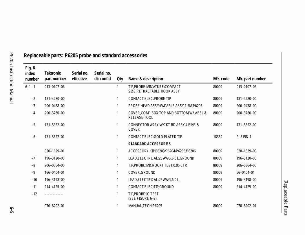
6–1 –1 013–0107–06 1 TIP,PROBE:MINIATURE/COMPACTSIZE,RETRACTABLE HOOK ASSY
80009 013–0107–06
–2 131–4280–00 1 CONTACT,ELEC:PROBE TIP 80009 131–4280–00
–3 206–0438–00 1 PROBE HEAD ASSY:W/CABLE ASSY,1.5M,P6205 80009 206–0438–00
–4 200–3760–00 1 COVER,COMP BOX:TOP AND BOTTOM,W/LABEL &RELEASE TOOL
80009 200–3760–00
–5 131–5352–00 1 CONNECTOR ASSY:W/CKT BD ASSY,4 PINS &COVER
80009 131–5352–00
–6 131–3627–01 1 CONTACT,ELEC:GOLD PLATED TIP 18359 P–6158–1
STANDARD ACCESSORIES
020–1629–01 1 ACCESSORY KIT:P6203/P6204/P6205/P6206 80009 020–1629–00
–7 196–3120–00 1 LEAD,ELECTRICAL:23 AWG,6.0 L,GROUND 80009 196–3120–00
–8 206–0364–00 1 TIP,PROBE:MICROCKT TEST,0.05 CTR 80009 206–0364–00
–9 166–0404–01 1 COVER,GROUND 80009 66–0404–01
–10 196–3198–00 1 LEAD,ELECTRICAL:26 AWG,6.0 L 80009 196–3198–00
–11 214–4125–00 1 CONTACT,ELEC:TIP,GROUND 80009 214–4125–00
–12 – – – – – – – 1 TIP,PROBE:IC TEST(SEE FIGURE 6–2)
070–8202–01 1 MANUAL,TECH:P6205 80009 070–8202–01
Replaceable Parts
6–6 P6205 Instruction Manual
Figu
re 6
–2: P
6205
pro
be o
ptio
nal a
cces
sorie
s

Replaceable P
arts
6–7P
6205 Instruction Manual
Replaceable parts: P6205 probe optional accessories
Fig. &indexnumber
Tektronixpart number
Serial no.effective
Serial no.discont’d Qty Name & description Mfr. code Mfr. part number
OPTIONAL ACCESSORIES
6–2 –1 003–1383–00 1 RLSE TOOL,COVER:COMP BOX,POLYCARBONATE TK2565 003–1383–00
–2 003–1433–00 1 SCREWDRIVER:ADJUSTMENT TOOL,METAL TIP TK2565 003–1433–00
003–1433–01 1 SCREWDRIVER:ADJUSTMENT TOOL,PKG OF 5 80009 003–1433–01
–3 015–0201–07 1 TIP,PROBE:IC TEST,PKG OF 10 80009 015–0201–07
015–0201–08 1 TIP,PROBE:IC TEST,PKG OF 100 80009 015–0201–08
–4 031–4353–00 1 CONNECTOR,PROBE:PACK OF 25 80009 031–4353–00
–5 – – – – – – – 1 SMG50,SMT KLIPCHIP:20 ADAPTERS
200–3760–00 1 COVER,COMP BOX:TOP AND BOTTOM,W/LABEL &RELEASE TOOL
80009 200–3760–00
–6 016–0633–00 1 MARKER SET,CA:2 EA VARIOUS COLORS 80009 016–0633–00
–7 015–0325–00 1 ADAPTER,PROBE:PROBE TO CONNECTOR PINS TK2565 015–0325–00
–8 013–0084–01 1 ADAPTER,CONN:BNC TO PROBE 24931 28P156–1
–9 017–0088–00 1 CONN,PLUG,ELEC:50 OHM,GR 80009 017–0088–00
–10 013–0085–00 1 TIP,PROBE:GROUNDING 80009 013–0085–00
–11 131–0258–00 1 CONN,RCPT,ELEC:MINIATURE TIP SIZE,TEST JACK 24931 33JR115–2

Replaceable Parts
6–8 P6205 Instruction Manual
Copyright © 2022 FDOKUMEN