16-Channel LED Driver With DOT Correction and Pre-Charge FET
27
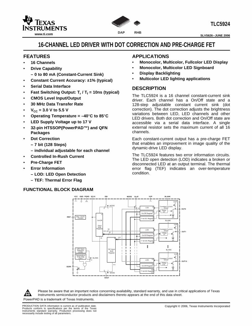
RHB DAP www.ti.com FEATURES APPLICATIONS DESCRIPTION FUNCTIONAL BLOCK DIAGRAM On/Off Input Shift Register DC Input Shift Register 7-bit DC Register Delay x0 Constant Current Driver LOD MODE 0 1 MODE 0 1 0 15 111 0 On/Off Register 0 6 0 0 0 1 Temperature Error Flag (TEF) LED Open Detection (LOD) 7-bit DC Register Delay x1 Constant Current Driver LOD On/Off Register 7 13 1 1 7-bit DC Register Delay x15 Constant Current Driver LOD On/Off Register 105 111 15 15 BLANK 0 Max. OUTn Current GND VCC SIN SCLK SOUT IREF XERR XLAT MODE OUT0 OUT1 OUT15 PGND BLANK BLANK BLANK 16 16 112 1 VUP VUP VUP VUP TLC5924 SLVS626 – JUNE 2006 16-CHANNEL LED DRIVER WITH DOT CORRECTION AND PRE-CHARGE FET • Monocolor, Multicolor, Fullcolor LED Display • 16 Channels • Monocolor, Multicolor LED Signboard • Drive Capability • Display Backlighting – 0 to 80 mA (Constant-Current Sink) • Multicolor LED lighting applications • Constant Current Accuracy: ±1% (typical) • Serial Data Interface • Fast Switching Output: T r /T f = 10ns (typical) The TLC5924 is a 16 channel constant-current sink • CMOS Level Input/Output driver. Each channel has a On/Off state and a • 30 MHz Data Transfer Rate 128-step adjustable constant current sink (dot correction). The dot correction adjusts the brightness • V CC = 3.0 V to 5.5 V variations between LED, LED channels and other • Operating Temperature = –40°C to 85°C LED drivers. Both dot correction and On/Off state are • LED Supply Voltage up to 17 V accessible via a serial data interface. A single external resistor sets the maximum current of all 16 • 32-pin HTSSOP(PowerPAD™) and QFN channels. Packages • Dot Correction Each constant-current output has a pre-charge FET that enables an improvement in image quality of the – 7 bit (128 Steps) dynamic-drive LED display. – individual adjustable for each channel The TLC5924 features two error information circuits. • Controlled In-Rush Current The LED open detection (LOD) indicates a broken or • Pre-Charge FET disconnected LED at an output terminal. The thermal • Error Information error flag (TEF) indicates an over-temperature condition. – LOD: LED Open Detection – TEF: Thermal Error Flag Please be aware that an important notice concerning availability, standard warranty, and use in critical applications of Texas Instruments semiconductor products and disclaimers thereto appears at the end of this data sheet. PowerPAD is a trademark of Texas Instruments. PRODUCTION DATA information is current as of publication date. Copyright © 2006, Texas Instruments Incorporated Products conform to specifications per the terms of the Texas Instruments standard warranty. Production processing does not necessarily include testing of all parameters.
-
Upload
khangminh22 -
Category
Documents
-
view
0 -
download
0
Transcript of 16-Channel LED Driver With DOT Correction and Pre-Charge FET
RHBDAPwww.ti.com
FEATURES APPLICATIONS
DESCRIPTION
FUNCTIONAL BLOCK DIAGRAM
On/Off
InputShift
Register
DC Input
ShiftRegister
7−bit DC Register
Delayx0
Constant CurrentDriverLOD
MODE
0 1
MODE
0 1
015
111
0On/Off Register
0
6
0
001
TemperatureError Flag
(TEF)
LED OpenDetection
(LOD)
7−bit DC Register
Delayx1
Constant CurrentDriver
LOD
On/Off Register
7
13
1
1
7−bit DC Register
Delayx15
Constant CurrentDriverLOD
On/Off Register
105
111
15
15BLANK
0
Max. OUTnCurrent
GNDVCC SINSCLK
SOUT
IREF
XERR
XLATMODE
OUT0
OUT1
OUT15
PGND BLANK
BLANK
BLANK
16
16
112
1
VUP
VUP
VUP
VUP
TLC5924
SLVS626–JUNE 2006
16-CHANNEL LED DRIVER WITH DOT CORRECTION AND PRE-CHARGE FET
• Monocolor, Multicolor, Fullcolor LED Display• 16 Channels• Monocolor, Multicolor LED Signboard• Drive Capability• Display Backlighting– 0 to 80 mA (Constant-Current Sink)• Multicolor LED lighting applications• Constant Current Accuracy: ±1% (typical)
• Serial Data Interface• Fast Switching Output: Tr / Tf = 10ns (typical)
The TLC5924 is a 16 channel constant-current sink• CMOS Level Input/Output driver. Each channel has a On/Off state and a• 30 MHz Data Transfer Rate 128-step adjustable constant current sink (dot
correction). The dot correction adjusts the brightness• VCC = 3.0 V to 5.5 Vvariations between LED, LED channels and other• Operating Temperature = –40°C to 85°C LED drivers. Both dot correction and On/Off state are
• LED Supply Voltage up to 17 V accessible via a serial data interface. A singleexternal resistor sets the maximum current of all 16• 32-pin HTSSOP(PowerPAD™) and QFNchannels.Packages
• Dot Correction Each constant-current output has a pre-charge FETthat enables an improvement in image quality of the– 7 bit (128 Steps)dynamic-drive LED display.
– individual adjustable for each channelThe TLC5924 features two error information circuits.• Controlled In-Rush CurrentThe LED open detection (LOD) indicates a broken or
• Pre-Charge FET disconnected LED at an output terminal. The thermal• Error Information error flag (TEF) indicates an over-temperature
condition.– LOD: LED Open Detection– TEF: Thermal Error Flag
Please be aware that an important notice concerning availability, standard warranty, and use in critical applications of TexasInstruments semiconductor products and disclaimers thereto appears at the end of this data sheet.
PowerPAD is a trademark of Texas Instruments.
PRODUCTION DATA information is current as of publication date. Copyright © 2006, Texas Instruments IncorporatedProducts conform to specifications per the terms of the TexasInstruments standard warranty. Production processing does notnecessarily include testing of all parameters.

www.ti.com
ABSOLUTE MAXIMUM RATINGS (1) (2)
RECOMMENDED OPERATING CONDITIONS—DC Characteristics
TLC5924
SLVS626–JUNE 2006
These devices have limited built-in ESD protection. The leads should be shorted together or the device placed in conductive foamduring storage or handling to prevent electrostatic damage to the MOS gates.
ORDERING INFORMATION (1)
TA Package Part Number (1)
32-pin, HTSSOP, PowerPAD™ TLC5924DAP–40°C to 85°C
32-pin, 5 mm x 5 mm QFN TLC5924RHB
(1) For the most current package and ordering information, see the Package Option Addendum at the endof this document, or see the TI website at www.ti.com.
TLC5924 UNIT
VCC Supply voltage (2) –0.3 to 6 V
VUP Pre-charge voltage –0.3 to 16 V
IO Output current (dc) I(OUT0) to I(OUT15) 90 mA
VI Input voltage range (2) V(BLANK), V(XLAT), V(SCLK), V(SIN), V(MODE), V(IREF) –0.3 to VCC + 0.3 V
V(SOUT), V(XERR) –0.3 to VCC + 0.3 VVO Output voltage range (2)
V(OUT0) to V(OUT15) -0.3 to VUP V
HBM (JEDEC JESD22-A114, Human Body Model) 2 kVESD rating
CDM (JEDEC JESD22-C101, Charged Device Model) 500 V
Tstg Storage temperature range –40 to 150 °C
HTSSOP (DAP) 42.54 mW/°CPower dissipation rating at (orabove) TA = 25°C (3) QFN (RHB) 27.86 mW/°C
(1) Stresses beyond those listed under absolute maximum ratings may cause permanent damage to the device. These are stress ratingsonly, and functional operation of the device at these or any other conditions beyond those indicated under recommended operatingconditions is not implied. Exposure to absolute-maximum-rated conditions for extended periods may affect device reliability.
(2) All voltage values are with respect to network ground terminal.(3) See SLMA002 for more information about PowerPAD™
MIN NOM MAX UNIT
VCC Supply voltage 3 5.5 V
VUP Pre-charge voltage 3 15 V
VO Voltage applied to output, (Out0 - Out15) VUP V
VIH High-level input voltage 0.8 VCC VCC V
VIL Low-level input voltage GND 0.2 VCC V
IOH High-level output current VCC = 5 V at SOUT –1 mA
IOL Low-level output current VCC = 5 V at SOUT, XERR 1 mA
IOLC Constant output current OUT0 to OUT15 80 mA
TA Operating free-air temperature range -40 85 °C
2 Submit Documentation Feedback

www.ti.com
RECOMMENDED OPERATING CONDITIONS—AC Characteristics
ELECTRICAL CHARACTERISTICS
TLC5924
SLVS626–JUNE 2006
VCC = 3 V to 5.5 V, TA = -40°C to 85°C (unless otherwise noted)
MIN TYP MAX UNIT
fSCLK Clock frequency SCLK 30 MHz
twh0, twl0 CLK pulse duration SCLK=H/L 16 ns
twh1 XLAT pulse duration XLAT=H 20 ns
tsu0 SIN to SCLK↑ (1) 10
tsu1 SLCK↑ to XLAT↓(dot correction data) 10
tsu1a Setup time SCLK↑to XLAT↑ (ON/OFF data) 10 ns
tsu2 MODE↑↓ to SCLK↑ 10
tsu3 MODE↑↓ to XLAT↑ 10
th0 SCLK↑ to SIN 10
th1 XLAT↓ to SCLK↑ (dot correction data) 10
th1a Hold time XLAT↑ to SCLK↑ (ON/OFF data) 10 ns
th2 SCLK↑to MODE↑↓ 10
th3 XLAT↓ to MODE↑↓ 10
(1) "↑" and "↓" indicates a rising edge, and a falling edge respectively.
VCC = 3 V to 5.5 V, TA = –40°C to 85°C (unless otherwise noted)
PARAMETER TEST CONDITIONS MIN TYP MAX UNIT
VOH High-level output voltage IOH = –1 mA, SOUT VCC– 0.5 V
VOL Low-level output voltage IOL = 1 mA, SOUT 0.5 V
II Input current VI = VCC or GND, BLANK, XLAT, SCLK, SIN, MODE –1 1 µA
No data transfer, All output OFF, VO = 1 V, R(IREF) = 10 6kΩ
No data transfer, All output OFF, VO = 1 V, R(IREF) = 1.3 15kΩICC Supply current mA
Data transfer 30 MHz, All output ON, VO = 1 V, 32R(IREF) = 1.3 kΩ
Data transfer 30 MHz, All output ON, VO = 1 V, 36 65 (1)R(IREF) = 600 Ω
IOLC Constant sink current All output ON, VO = 1 V, R(IREF) = 600 Ω 70 80 90 mA
All output OFF, VO = 15 V, R(IREF) = 600 Ω, OUT0 toILO0 0.1 µAOUT15Leakage output currentILO1 VXERR = 5.5 V, No TEF and LOD 10 µA
∆IOLC0 Constant sink current error All output ON, VO = 1 V, R(IREF) = 600 Ω, OUT0 to OUT15 ±1% ± 4%
device to device, averaged current from OUT0 to OUT15,∆IOLC1 Constant sink current error ±4% ±8.5%R(IREF) = 600 Ω
All output ON, VO = 1 V, R(IREF) = 600 Ω,∆IOLC2 Line regulation ±1 ±4 %/VOUT0 to OUT15, VCC = 3 V to 5.5 V
All output ON, VO = 1 V to 3 V, R(IREF) = 600 Ω,∆IOLC3 Load regulation ±2 ±6 %/VOUT0 to OUT15
R(ON) Pre-charge FET on-resistance VUP = 3 V, VO = 0 V, OUT0 to OUT15 10 KΩ
T(TEF) Thermal error flag threshold Junction temperature, rising temperature (2) 150 160 180 °C
V(LOD) LED open detection threshold 0.3 0.4 V
V(IREF) Reference voltage output R(IREF) = 600 Ω 1.20 1.24 1.28 V
(1) Measured at device start-up temperature. Once the IC is operating (self heating), lower ICC values will be seen. See Figure 20.(2) Not tested. Specified by design.
3Submit Documentation Feedback

www.ti.com
DISSIPATION RATINGS
SWITCHING CHARACTERISTICS
1
2
3
4
5
6
7
8
9
10
11
12
13
14
15
16
32
31
30
29
28
27
26
25
24
23
22
21
20
19
18
17
GND
BLANK
XLAT
SCLK
SIN
VUP
OUT0
OUT1
PGND
OUT2
OUT3
OUT4
OUT5
PGND
OUT6
OUT7
VCC
IREF
MODE
XERR
SOUT
VUP
OUT15
OUT14
PGND
OUT13
OUT12
OUT11
OUT10
PGND
OUT9
OUT8
THERMAL
PAD
SO
UT
24
VU
P2
3
OU
T15
22
OU
T14
21
PG
ND
20
OU
T13
19
OU
T12
18
OU
T11
17
OUT1016
PGND15
OUT914
OUT813
OUT712
OUT611
PGND10
OUT59
OU
T4
8
OU
T3
7
OU
T2
6
PG
ND
5
OU
T1
4
OU
T0
3
VU
P2
SIN
1
XERR 25
MODE 26
IREF 27
VCC 28
GND 29
BLANK 30
XLAT 31
SCLK 32
RHB PACKAGE
(TOP VIEW)
(QFN)
DAP PACKAGE
(TOP VIEW)
TLC5924
SLVS626–JUNE 2006
POWER RATING DERATING FACTOR POWER RATING POWER RATINGPACKAGE TA < 25°C ABOVE TA = 25°C TA = 70°C TA = 85°C
32-pin HTSSOP with PowerPAD (1) 5318 mW 42.54 mW/°C 3403 mW 2765 mWsoldered
32-pin HTSSOP with PowerPAD (1) 2820 mW 22.56 mW/°C 1805 mW 1466 mWunsoldered
32-pin QFN 3482 mW 27.86 mW/°C 2228 mW 1811 mW
(1) The PowerPAD is soldered to the PCB with a 2 oz. copper trace. See SLMA002 for further information.
PARAMETER TEST CONDITIONS MIN TYP MAX UNIT
tr0 SOUT(see (1)) 16Rise time ns
tr1 OUTn, VCC = 5 V, TA = 60°C, DCx = 7F (see (2) ) 10 30
tf0 SOUT (see (1)) 16Fall time ns
tf1 OUTn, VCC = 5 V, TA = 60°C, DCx = 7F (see (2)) 10 30
tpd0 SCLK↑ to SOUT↑↓ (see (3) (4)) 30
tpd1 MODE↑↓ to SOUT↑↓ (see (3)) 30
tpd2 BLANK↑↓ to OUT0↑↓ (see (5)), Sink current On/Off 80Propagation delay time ns
tpd3 XLAT↑ to OUT0↑↓ (see (5)) 60
tpd4 OUTn↑↓ to XERR↑↓ (see (6)) 1000
tpd5 XLAT↑ to IOUT(dot-correction) (see (7)) 1000
td Output delay time OUTn↑ to OUT(n+1)↑, OUTn ↓ to OUT(n+1)↓ (see (5)) 14 22 30 ns
(1) See Figure 4. Defined as from 10% to 90%(2) See Figure 5. Defined as from 10% to 90%(3) See Figure 4, Figure 16(4) "↑" and "↓" indicates a rising edge, and a falling edge respectively.(5) See Figure 5 and Figure 16(6) See Figure 5, Figure 6, and Figure 16(7) See Figure 5
4 Submit Documentation Feedback

www.ti.com
TLC5924
SLVS626–JUNE 2006
Terminal Functions
TERMINAL
NO. I/O DESCRIPTIONNAME
TSSOP QFN
Blank (Light OFF). When BLANK=H, All OUTn outputs are forced to VUP level. WhenBLANK 2 30 I BLANK=L, ON/OFF of OUTn outputs are controlled by input data.
GND 1 29 Ground
IREF 31 27 I/O Reference current terminal
Mode select. When MODE=L, SIN, SOUT, SCLK, XLAT are connected to ON/OFF controlMODE 30 26 I logic. When MODE=H, SIN, SOUT, SCLK, XLAT are connected to dot-correction logic.
OUT0 7 3 O Constant current output
OUT1 8 4 O Constant current output
OUT2 10 6 O Constant current output
OUT3 11 7 O Constant current output
OUT4 12 8 O Constant current output
OUT5 13 9 O Constant current output
OUT6 15 11 O Constant current output
OUT7 16 12 O Constant current output
OUT8 17 13 O Constant current output
OUT9 18 14 O Constant current output
OUT10 20 16 O Constant current output
OUT11 21 17 O Constant current output
OUT12 22 18 O Constant current output
OUT13 23 19 O Constant current output
OUT14 25 21 O Constant current output
OUT15 26 22 O Constant current output
9, 14, 5, 10,PGND Power ground19, 24 15, 20
VUP 6, 27 2, 23 Pre-charge power supply voltage
Data shift clock. Note that the internal connections are switched by MODE (pin #30). AtSCLK 4 32 I SCLK↑, the shift-registers selected by MODE shift the data.
SIN 5 1 I Data input of serial I/F
SOUT 28 24 O Data output of serial I/F
VCC 32 28 Power supply voltage
Error output. XERR is open drain terminal. XERR transistions from H to L when LOD or TEFXERR 29 25 O detected.
Data latch signal. When MODE = L (ON/OFF data mode), XLAT is an edge-triggered latchsignal of ON/OFF registers. The serial data in ON/OFF input shift registers is latched into theON/OFF registers at the rising edge of XLAT. When MODE = H (DC data mode), XLAT is aXLAT 3 31 I level-triggered latch signal of dot correction registers. The serial data in DC input shiftregisters is written into dot correction registers when XLAT = H. The data in dot correctionregisters is held constant when XLAT = L.
5Submit Documentation Feedback

www.ti.com
PIN EQUIVALENT INPUT AND OUTPUT SCHEMATIC DIAGRAMS
(Note: Resistor values are equivalent resistance and not tested).
VCC
INPUT
GND
400
SOUT
GND
10
XERR
GND
20
PARAMETER MEASUREMENT INFORMATION
SOUT
15 pF
OUTn
VUP
51 Ω
15 pF
TLC5924
SLVS626–JUNE 2006
Figure 1. Input Equivalent Circuit (BLANK, XLAT, SCLK, SIN, MODE)
Figure 2. Output Equivalent Circuit
Figure 3. Output Equivalent Circuit (XERR)
Figure 4. Test Circuit for tr0, tf0, tpd0, tpd1
Figure 5. Test Circuit for tr1, tf1, tpd2, tpd3, tpd5, ttd
6 Submit Documentation Feedback

www.ti.com
XERR
470 kΩ
TLC5924
SLVS626–JUNE 2006
PARAMETER MEASUREMENT INFORMATION (continued)
Figure 6. Test Circuit for tpd4
7Submit Documentation Feedback

www.ti.com
PRINCIPLES OF OPERATION
Setting Maximum Channel Current
IMAX VIREFRIREF
40(1)
Setting Dot-Correction
IOutn IMAX DCn
127 (2)
DC 15.0
105
DC 15.6
111
DC 14.6
104
MSB
DC OUT15
DC 0.0
0
DC 1.0
7
DC 0.6
6
LSB
DC OUT0DC OUT14 − DC OUT1
TLC5924
SLVS626–JUNE 2006
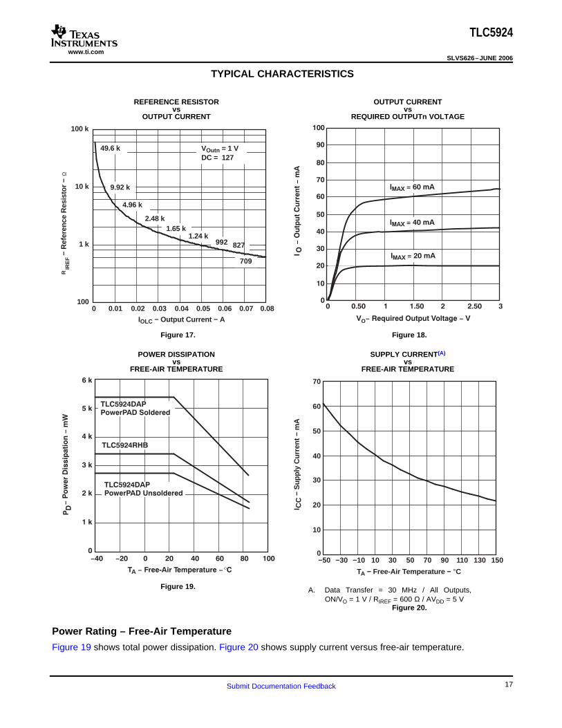
The maximum output current per channel is set by a single external resistor, R(IREF), which is placed betweenIREF and GND. The voltage on IREF is set by an internal band gap V(IREF) with a typical value of 1.24V. Themaximum channel current is equivalent to the current flowing through R(IREF) multiplied by a factor of 40. Themaximum output current per channel can be calculated by Equation 1:
where:
VIREF = 1.24V typ.
RIREF = User selected external resistor ®IREF should not be smaller than 600 Ω)
Figure 17 shows the maximum output current, IOLC, versus R(IREF) . In Figure 17, R(IREF) is the value of theresistor between IREF terminal to ground, and IOLC is the constant output current of OUT0,.....OUT15. A variablepower supply may be connected to the IREF pin through a resistor to change the maximum output current perchannel. The maximum output per channel is 40 times the current flowing out of the IREF pin. The maximumcurrent from IREF equals 1.24V/600Ω.
The TLC5924 has the capability to fine adjust the current of each channel, OUT0 to OUT15 independently. Thisis also called dot correction. This feature is used to adjust the brightness deviations of LED connected to theoutput channels OUT0 to OUT15. Each of the 16 channels can be programmed with a 7-bit word. The channeloutput can be adjusted in 128 steps from 0% to 100% of the maximum output current IMAX. Dot correction for allchannels must be entered at the same time. Equation 2 determines the output current for each OUTn:
where:
IMax = the maximum programmable current of each output
DCn = the programmed dot-correction value for output n (DCn = 0, 1, 2 ...127)
n = 0, 1, 2 ... 15
Dot correction data are entered for all channels at the same time. The complete dot correction data formatconsists of 16 x 7-bit words, which forms a 112-bit wide serial data packet. The channel data is put one afteranother. All data is clocked in with MSB first. Figure 7 shows the DC data format. The DC15.6 in Figure 7 standsfor the 6th most significant bit for output 15.
Figure 7. DC Data Format
To input data into dot correction register, MODE must be set to high. The internal input shift register is then setto 112-bit width. After all serial data is clocked in, a high level pulse of XLAT signal connects the serial data tothe dot correction register. The dot correction registers are level-triggered latches of XLAT signal. The serialdata is latched into the dot correction registers when XLAT goes low. The data in dot correction registers is heldconstant when XLAT is low. BLANK signal does not need to be high to latch in new data. Since XLAT is alevel-triggered signal when MODE is high, SCLK and SIN must not be changed while XLAT is high. (Figure 16).
8 Submit Documentation Feedback

www.ti.com
Output Enable
Setting Channel On/Off Status
On/Off Data
15
MSB
On/Off
OUT15
On/Off
OUT14
On/Off
OUT13
0
LSB
On/Off
OUT2
On/Off
OUT1
On/Off
OUT0
Delay Between Outputs
Pre-Charge FET On/Off Timing
TLC5924
SLVS626–JUNE 2006
PRINCIPLES OF OPERATION (continued)
When BLANK = H, TLC5924 switches off the sink current of all OUTn with each output delay, then switches onthe pre-charge FET of all OUTn. When BLANK = L, the TLC5924 switches off the pre-charge FETs, and enablesthe sink current set by input data. See "Delay Between Outputs" section for more detail on the output delay.
Table 1. BLANK Signal Truth Table
BLANK OUT0 - OUT15
LOW Normal condition
HIGH VUP
All OUTn channels of TLC5924 can be switched on or off independently. Each of the channels can beprogrammed with a 1-bit word. On/Off data are entered for all channels at the same time. The complete On/Offdata format consists of 16 x 1-bit words, which form a 16-bit wide data packet. The channel data is put one afteranother. All data is clocked in with MSB first. Figure 8 shows the On/Off data format.
Figure 8. On/Off Data Format
To input On/Off data into On/Off register MODE must be set to low. The internal input shift register is then set to16 bit width. After all serial data is clocked in, a rising edge of XLAT is used to latch data into the On/Offregister. The ON/OFF register is an edge-triggered latch of XLAT signal. BLANK signal does not need to be highto latch in new data. Figure 16 shows the On/Off data input timing chart.
The TLC5924 has graduated delay circuits between outputs. These delay circuits can be found in the constantcurrent block of the device (see Functional Block Diagram). The fixed delay time is 20 ns (typical), OUT0 has nodelay, OUT1 has 20 ns delay, OUT2 has 40 ns delay, etc. This delay prevents large inrush currents, whichreduce power supply bypass capacitor requirements when the outputs turn on. The delay works during switch onand switch off of each output channel. LEDs that have not turned on before BLANK is pulled high will still turn onand off at the determined delayed time regardless of the state of BLANK. Therefore, every LED will beilluminated for the amount of time BLANK is low.
The pre-charge FETs turn on at the same time; and, they turn on at the time the last output that is on turns off.
All pre-charge FETs turn off just after BLANK signal becomes low level, regardless of on/off data of each output.Figure 9 shows the example of BLANK and OUTn timing.
9Submit Documentation Feedback

www.ti.com
tpd2tpd2
VUP
Pre-charge Period
ONCurrent ON OFF
BLANK
OUT0
OUT14
OUT15
ONOFF
t x 14d t x 14d
VUP: Pre-Charge Power Supply
VUPVUP
TLC5924
Pre-Charge Power Supply
Serial Interface Data Transfer Rate
TLC5924
SLVS626–JUNE 2006
Figure 9. Timing Chart of BLANK and OUTn(On/Off Data Condition: OUT0=H, OUT14=H, OUT15=L)
VUP is a pre-charge power supply terminal. The pre-charge voltage should be supplied to this terminal fornormal operation. When VUP terminal is open, TLC5924 keeps OUT0-15 open. TLC5924 has two VUP pins asshown in the Terminal Functions Table. Both VUP pins should be connected to the pre-charge power supply asshown in Figure 10.
Figure 10. VUP Power Supply
The TLC5924 includes a flexible serial interface, which can be connected to a microcontroller or digital signalprocessor. Only 3 pins are required to input data into the device. The rising edge of SCLK signal shifts the datafrom SIN pin to internal shift register. After all data is clocked in, a rising edge of XLAT latches the serial data tothe internal registers. All data is clocked in with MSB first. Multiple TLC5924 devices can be cascaded byconnecting SOUT pin of one device with SIN pin of following device. The SOUT pin can also be connected tocontroller to receive LOD information from TLC5924.
10 Submit Documentation Feedback

www.ti.com
TLC5924
SIN SOUT
OUT0 OUT15
SCLK
MODE
XLAT
BLANK IREF
XERR
TLC5924
SIN SOUT
OUT0 OUT15
SCLK
MODE
XLAT
BLANK IREF
XERR
IC 0 IC n
5
SIN
SCLK
MODE
XLAT
BLANK
XERR
Controller
SOUT
100 k
100 nF
V(LED)V(LED)V(LED)V(LED)VCC
100 nF
VCC VCC
f_(SCLK) 112 f_(update) n (3)
Operating Modes
TLC5924
SLVS626–JUNE 2006
Figure 11. Cascading Devices
Figure 11 shows a example application with n cascaded TLC5924 devices connected to a controller. Themaximum number of cascaded TLC5924 devices depends on application system and data transfer rate.Equation 3 calculates the minimum data input frequency needed.
where:
f_(SCLK): The minimum data input frequency for SCLK and SIN.
f_(update): The update rate of the whole cascaded system.
n: The number of cascaded TLC5924 devices.
The TLC5924 has different operating modes depending on MODE signal. Table 2 shows the available operatingmodes. The values in the input shift registers, DC register and On/Off register are unknown just after power on.The DC and On/Off register values should be properly stored through the serial interface before starting theoperation.
Table 2. TLC5924 Operating Modes Truth Table
MODE SIGNAL INPUT SHIFT REGISTER MODE
LOW 16 bit On/Off Mode
HIGH 112 bit Dot Correction Data Input Mode
11Submit Documentation Feedback

www.ti.com
Error Information Output
TEF: Thermal Error Flag
LOD: LED-Open Detection
LOD Data
0
LSB
OUT2 OUT1 OUT0
LOD LOD LOD
15
MSB
LOD
OUT15 OUT14 OUT13
LODLOD
TLC5924
SLVS626–JUNE 2006
The open-drain output XERR is used to report both of the TLC5924 error flags, TEF and LOD. During normaloperating conditions, the internal transistor connected to the XERR pin is turned off. The voltage on XERR ispulled up to VCC through a external pull-up resistor. If TEF or LOD is detected, the internal transistor is turnedon, and XERR is pulled to GND. Since XERR is an open-drain output, multiple ICs can be OR'ed together andpulled up to VCC with a single pull-up resistor. This reduces the number of signals needed to report a systemerror.
To differentiate LOD and TEF signal from XERR pin, LOD can be masked out with BLANK = HIGH.
Table 3. XERR Truth Table
CONDITION ERROR INFORMATION XERR
TEMPERATURE BLANK OUTn VOLTAGE TEF LODn
TJ < T(TEF) H Don't Care L L High-Z (1)
TJ > T(TEF) H L
TJ < T(TEF) L OUTn > V(LOD) L L High-Z
OUTn < V(LOD) H L
TJ > T(TEF) OUTn > V(LOD) H L L
OUTn < V(LOD) H L
(1) Note: High-Z means high impedance
The TLC5924 provides a temperature error flag (TEF) circuit to indicate an over-temperature condition of the IC.If the junction temperature exceeds the threshold temperature T(TEF) (160°C typical), TEF becomes H and XERRpin goes to low level. When the junction temperature becomes lower than the threshold temperature, TEFbecomes L and XERR pin becomes high impedance.
The TLC5924 has an LED-open detector to detect broken or disconnected LEDs, which should be connected tothe output. The LED-open detector pulls the XERR pin down to GND when the LED open is detected. An openLED is detected when the following three conditions are met:1. BLANK is low2. On/Off data is high3. The voltage of OUTn is less than 0.3 V (typical)
The LOD status of each output can also be read out from the SOUT pin. Figure 12 shows the LOD data format.Table 4 shows the LOD truth table.
Figure 12. LOD Data Format
12 Submit Documentation Feedback

www.ti.com
Key Timing Requirements to Reading LOD
TLC5924
SLVS626–JUNE 2006
Table 4. LOD Data Truth Table
LED ON/OFF LOD BIT
Good On 0
Good Off 0
Bad On 1
Bad Off 0
• LOD status flagThe LOD status flag becomes active if the output voltage is <0.3 V (typical) when the output sink currentturns on. There is a 1-µs time delay from the time the output sink current turns on until the time the LODstatus flag becomes valid. The timing for each channel’s LOD status to become valid is shifted by the 30 nschannel-to-channel turn-on time. After BLANK goes low, OUT0 LOD status is valid when tpd2 + tpd4 = 60ns + 1 µs = 1.06 µs. OUT1 LOD status is valid when tpd2 + tpd4 + td = 60 ns + 1 µs + 30 ns = 1.09 µs.OUT3 LOD status is valid when tpd2 + tpd4 + 2*td = 1.12 µs, and so on.
• LOD internal latchThe TLC5924 has an internal latch to hold each channel’s LOD status flag information, as shown inFigure 13. When MODE is low, the LOD status information is latched into this latch on the rising edge ofXLAT. This is an edge-triggered latch. To ensure that a valid LOD status flag is latched, BLANK must be lowwhen XLAT goes high. After the rising edge of XLAT, changes in the status flags do not affect the values inthe LOD latch.
• Loading LOD data to the input shift registerThe LOD data must be transferred to the input shift register before it is available to be clocked out of SOUT.The internal shift register has a set/reset function that is controlled by the LOD internal latch. While XLAT ishigh, the LOD internal latch holds the input shift register in either set or reset, depending on the value in thelatch. This effectively puts the LOD data into the input shift register where it remains as long as XLAT ishigh. The values in the input shift register are unaffected by any other signals, including SIN and SCLK whileXLAT is high. During this time, the status of OUT15 is present on SOUT.
• Latching LOD data into the internal shift registerWhile XLAT is high, the status of OUT15 is present on SOUT. When XLAT transitions low, all data is latchedinto the Input shift register, and the LOD internal latch is disconnected from the internal shift register.
• Clocking LOD data out of SOUTWhile XLAT is low and SCLK is low, the status of OUT15 is on SOUT. On the next rising edge of SCLK, thestatus of OUT14 shifts to SOUT. Each subsequent rising edge of SCLK shifts the LOD data out of SOUT.XLAT must stay low until all LOD data is clocked out of SOUT. See Shifting the LOD Data Out section formore details.
13Submit Documentation Feedback
www.ti.com
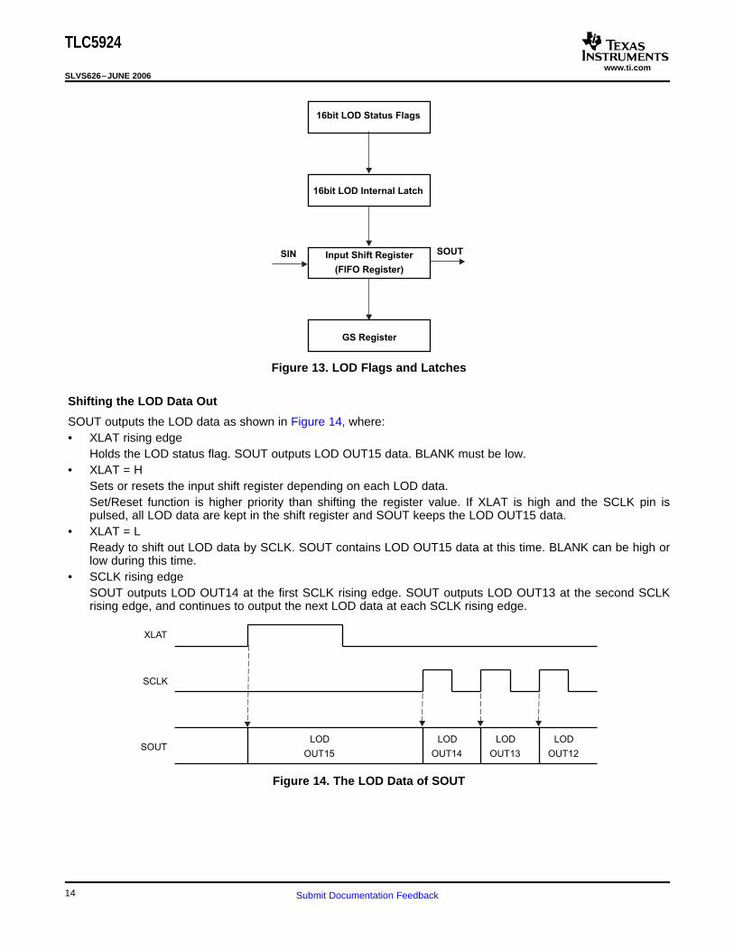
16bit LOD Status Flags
16bit LOD Internal Latch
Input Shift Register
GS Register
SIN SOUT
(FIFO Register)
Shifting the LOD Data Out
XLAT
SCLK
SOUTLOD
OUT15
LOD
OUT14
LOD
OUT12
LOD
OUT13
TLC5924
SLVS626–JUNE 2006
Figure 13. LOD Flags and Latches
SOUT outputs the LOD data as shown in Figure 14, where:• XLAT rising edge
Holds the LOD status flag. SOUT outputs LOD OUT15 data. BLANK must be low.• XLAT = H
Sets or resets the input shift register depending on each LOD data.Set/Reset function is higher priority than shifting the register value. If XLAT is high and the SCLK pin ispulsed, all LOD data are kept in the shift register and SOUT keeps the LOD OUT15 data.
• XLAT = LReady to shift out LOD data by SCLK. SOUT contains LOD OUT15 data at this time. BLANK can be high orlow during this time.
• SCLK rising edgeSOUT outputs LOD OUT14 at the first SCLK rising edge. SOUT outputs LOD OUT13 at the second SCLKrising edge, and continues to output the next LOD data at each SCLK rising edge.
Figure 14. The LOD Data of SOUT
14 Submit Documentation Feedback

www.ti.com
MODE
XLAT
SCLK
SIN
BLANK
OUT0
XERR
At the rising edge of XLAT while BLANK=L, LOD status is latched into
the internal edge-triggered register.
tpd2: 60ns max
td x 15 = 450ns max
tpd4: 1000ns max
1510ns max
LED open
When XLAT=H, the internal edge-triggered register
sets or resets the input shift register.
>1000ns
tpd2: 60ns max
td x 15 = 450ns max
tpd4: 1000ns max
1510ns max
>1000ns
OUT15
SOUT
TLC5924
SLVS626–JUNE 2006
Figure 15 shows the timing chart of reading LOD data.
Figure 15. Timing Chart of Reading LOD Data
15Submit Documentation Feedback

www.ti.com
SC
LK
SO
UT
SIN
MO
DE
XL
AT
On
/Off
Mo
de D
ata
Inp
ut
Cycle
DC
Mo
de D
ata
In
pu
t C
ycle
BL
AN
K
XE
RR
OU
T0
OU
T1
DC
Mo
de D
ata
In
pu
t
Cycle
On
/Off
Mo
de D
ata
Inp
ut
Cyc
le
On
/Off
Mo
de
Data
Inp
ut
Cycle
tw
h1
f SC
LK
tw
l0
t su1
tw
h0
t h0
t pd0
t h2
t su2
th1
th3
t pd1
tpd1
t su3
th3
t su3
t pd2
t pd4
td
tpd5
t pd2
t pd5
t pd3
On/O
ffLS
B
On/O
ffM
SB
DC
MS
BMS
BD
CLS
B
DC
MS
B
DC
MS
BD
CLS
B
DC
MS
BO
n/O
ffM
SBOn
/Off
MS
BLS
B On
/Off
MS
B
On/O
ffM
SB O
n/O
ffM
SBO
n/O
ff
DC
LS
BD
CLS
BO
n/O
ffLS
B
DC
On/O
ffM
SB
−1
tsu0
(cu
rren
t)
(cu
rren
t)
t d
t su1a
t h1a
TLC5924
SLVS626–JUNE 2006
Figure 16. Timing Chart Example for ON/OFF Setting to Dot-Correction
16 Submit Documentation Feedback
www.ti.com
TYPICAL CHARACTERISTICS
0
10
20
30
40
50
60
70
80
90
100
0 0.50 1 1.50 2 2.50 3
I O−
Ou
tpu
t C
urr
en
t−
mA
V − Required Output VO
oltage − V
IMAX = 60 mA
IMAX = 40 mA
IMAX = 20 mA
827
100
1 k
10 k
100 k
0.01 0.02 0.03 0.04 0.05 0.06 0.07 0.080
49.6 k
9.92 k
4.96 k
2.48 k1.65 k
1.24 k
709
− R
efer
ence
Res
isto
r −
IOLC − Output Current − A
RIR
EF
Ω
VOutn = 1 VDC = 127
992
3 k
2 k
1 k
0−40 −20 0 20 40
4 k
5 k
6 k
60 80 100
TA − Free-Air Temperature −°C
−P
ow
er
Dis
sip
ati
on
−m
WP
D
TLC5924DAPPowerPAD Soldered
TLC5924RHB
TLC5924DAPPowerPAD Unsoldered
0
10
20
30
40
50
60
70
−50 −30 −10 10 30 50 70 90 110 130 150
I CC
− S
uppl
y C
urre
nt −
mA
TA − Free-Air T emperature − °C
Power Rating – Free-Air Temperature
TLC5924
SLVS626–JUNE 2006
REFERENCE RESISTOR OUTPUT CURRENTvs vs
OUTPUT CURRENT REQUIRED OUTPUTn VOLTAGE
Figure 17. Figure 18.
POWER DISSIPATION SUPPLY CURRENT(A)
vs vsFREE-AIR TEMPERATURE FREE-AIR TEMPERATURE
Figure 19. A. Data Transfer = 30 MHz / All Outputs,ON/VO = 1 V / RIREF = 600 Ω / AVDD = 5 V
Figure 20.
Figure 19 shows total power dissipation. Figure 20 shows supply current versus free-air temperature.
17Submit Documentation Feedback

PACKAGING INFORMATION
Orderable Device Status (1) PackageType
PackageDrawing
Pins PackageQty
Eco Plan (2) Lead/Ball Finish MSL Peak Temp (3)
TLC5924DAP ACTIVE HTSSOP DAP 32 46 Green (RoHS &no Sb/Br)
CU NIPDAU Level-3-260C-168 HR
TLC5924DAPG4 ACTIVE HTSSOP DAP 32 46 Green (RoHS &no Sb/Br)
CU NIPDAU Level-3-260C-168 HR
TLC5924DAPR ACTIVE HTSSOP DAP 32 2000 Green (RoHS &no Sb/Br)
CU NIPDAU Level-3-260C-168 HR
TLC5924DAPRG4 ACTIVE HTSSOP DAP 32 2000 Green (RoHS &no Sb/Br)
CU NIPDAU Level-3-260C-168 HR
TLC5924RHBR ACTIVE QFN RHB 32 3000 Green (RoHS &no Sb/Br)
CU NIPDAU Level-2-260C-1 YEAR
TLC5924RHBRG4 ACTIVE QFN RHB 32 3000 Green (RoHS &no Sb/Br)
CU NIPDAU Level-2-260C-1 YEAR
TLC5924RHBT ACTIVE QFN RHB 32 250 Green (RoHS &no Sb/Br)
CU NIPDAU Level-2-260C-1 YEAR
TLC5924RHBTG4 ACTIVE QFN RHB 32 250 Green (RoHS &no Sb/Br)
CU NIPDAU Level-2-260C-1 YEAR
(1) The marketing status values are defined as follows:ACTIVE: Product device recommended for new designs.LIFEBUY: TI has announced that the device will be discontinued, and a lifetime-buy period is in effect.NRND: Not recommended for new designs. Device is in production to support existing customers, but TI does not recommend using this part ina new design.PREVIEW: Device has been announced but is not in production. Samples may or may not be available.OBSOLETE: TI has discontinued the production of the device.
(2) Eco Plan - The planned eco-friendly classification: Pb-Free (RoHS), Pb-Free (RoHS Exempt), or Green (RoHS & no Sb/Br) - please checkhttp://www.ti.com/productcontent for the latest availability information and additional product content details.TBD: The Pb-Free/Green conversion plan has not been defined.Pb-Free (RoHS): TI's terms "Lead-Free" or "Pb-Free" mean semiconductor products that are compatible with the current RoHS requirementsfor all 6 substances, including the requirement that lead not exceed 0.1% by weight in homogeneous materials. Where designed to be solderedat high temperatures, TI Pb-Free products are suitable for use in specified lead-free processes.Pb-Free (RoHS Exempt): This component has a RoHS exemption for either 1) lead-based flip-chip solder bumps used between the die andpackage, or 2) lead-based die adhesive used between the die and leadframe. The component is otherwise considered Pb-Free (RoHScompatible) as defined above.Green (RoHS & no Sb/Br): TI defines "Green" to mean Pb-Free (RoHS compatible), and free of Bromine (Br) and Antimony (Sb) based flameretardants (Br or Sb do not exceed 0.1% by weight in homogeneous material)
(3) MSL, Peak Temp. -- The Moisture Sensitivity Level rating according to the JEDEC industry standard classifications, and peak soldertemperature.
Important Information and Disclaimer:The information provided on this page represents TI's knowledge and belief as of the date that it isprovided. TI bases its knowledge and belief on information provided by third parties, and makes no representation or warranty as to theaccuracy of such information. Efforts are underway to better integrate information from third parties. TI has taken and continues to takereasonable steps to provide representative and accurate information but may not have conducted destructive testing or chemical analysis onincoming materials and chemicals. TI and TI suppliers consider certain information to be proprietary, and thus CAS numbers and other limitedinformation may not be available for release.
In no event shall TI's liability arising out of such information exceed the total purchase price of the TI part(s) at issue in this document sold by TIto Customer on an annual basis.
PACKAGE OPTION ADDENDUM
www.ti.com 31-Mar-2008
Addendum-Page 1

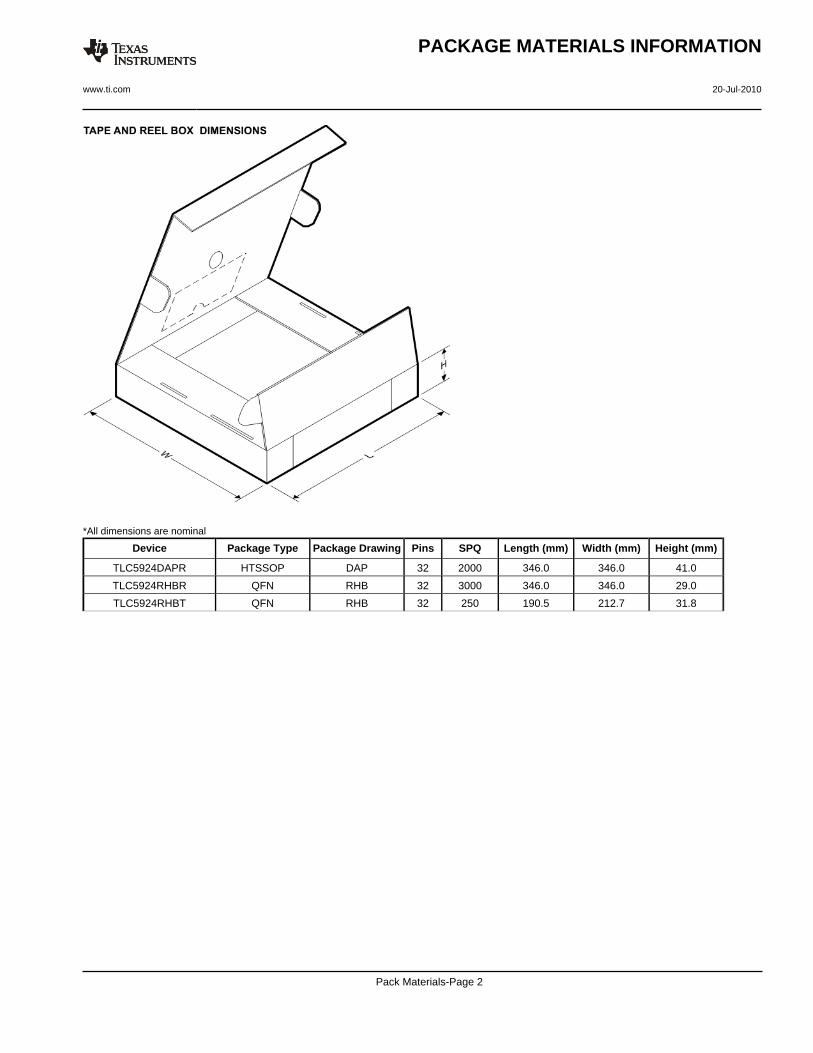
TAPE AND REEL INFORMATION
*All dimensions are nominal
Device PackageType
PackageDrawing
Pins SPQ ReelDiameter
(mm)
ReelWidth
W1 (mm)
A0(mm)
B0(mm)
K0(mm)
P1(mm)
W(mm)
Pin1Quadrant
TLC5924DAPR HTSSOP DAP 32 2000 330.0 24.4 8.6 11.5 1.6 12.0 24.0 Q1
TLC5924RHBR QFN RHB 32 3000 330.0 12.4 5.3 5.3 1.5 8.0 12.0 Q2
TLC5924RHBT QFN RHB 32 250 180.0 12.4 5.3 5.3 1.5 8.0 12.0 Q2
PACKAGE MATERIALS INFORMATION
www.ti.com 20-Jul-2010
Pack Materials-Page 1
*All dimensions are nominal
Device Package Type Package Drawing Pins SPQ Length (mm) Width (mm) Height (mm)
TLC5924DAPR HTSSOP DAP 32 2000 346.0 346.0 41.0
TLC5924RHBR QFN RHB 32 3000 346.0 346.0 29.0
TLC5924RHBT QFN RHB 32 250 190.5 212.7 31.8
PACKAGE MATERIALS INFORMATION
www.ti.com 20-Jul-2010
Pack Materials-Page 2


IMPORTANT NOTICE
Texas Instruments Incorporated and its subsidiaries (TI) reserve the right to make corrections, modifications, enhancements, improvements,and other changes to its products and services at any time and to discontinue any product or service without notice. Customers shouldobtain the latest relevant information before placing orders and should verify that such information is current and complete. All products aresold subject to TI’s terms and conditions of sale supplied at the time of order acknowledgment.
TI warrants performance of its hardware products to the specifications applicable at the time of sale in accordance with TI’s standardwarranty. Testing and other quality control techniques are used to the extent TI deems necessary to support this warranty. Except wheremandated by government requirements, testing of all parameters of each product is not necessarily performed.
TI assumes no liability for applications assistance or customer product design. Customers are responsible for their products andapplications using TI components. To minimize the risks associated with customer products and applications, customers should provideadequate design and operating safeguards.
TI does not warrant or represent that any license, either express or implied, is granted under any TI patent right, copyright, mask work right,or other TI intellectual property right relating to any combination, machine, or process in which TI products or services are used. Informationpublished by TI regarding third-party products or services does not constitute a license from TI to use such products or services or awarranty or endorsement thereof. Use of such information may require a license from a third party under the patents or other intellectualproperty of the third party, or a license from TI under the patents or other intellectual property of TI.
Reproduction of TI information in TI data books or data sheets is permissible only if reproduction is without alteration and is accompaniedby all associated warranties, conditions, limitations, and notices. Reproduction of this information with alteration is an unfair and deceptivebusiness practice. TI is not responsible or liable for such altered documentation. Information of third parties may be subject to additionalrestrictions.
Resale of TI products or services with statements different from or beyond the parameters stated by TI for that product or service voids allexpress and any implied warranties for the associated TI product or service and is an unfair and deceptive business practice. TI is notresponsible or liable for any such statements.
TI products are not authorized for use in safety-critical applications (such as life support) where a failure of the TI product would reasonablybe expected to cause severe personal injury or death, unless officers of the parties have executed an agreement specifically governingsuch use. Buyers represent that they have all necessary expertise in the safety and regulatory ramifications of their applications, andacknowledge and agree that they are solely responsible for all legal, regulatory and safety-related requirements concerning their productsand any use of TI products in such safety-critical applications, notwithstanding any applications-related information or support that may beprovided by TI. Further, Buyers must fully indemnify TI and its representatives against any damages arising out of the use of TI products insuch safety-critical applications.
TI products are neither designed nor intended for use in military/aerospace applications or environments unless the TI products arespecifically designated by TI as military-grade or "enhanced plastic." Only products designated by TI as military-grade meet militaryspecifications. Buyers acknowledge and agree that any such use of TI products which TI has not designated as military-grade is solely atthe Buyer's risk, and that they are solely responsible for compliance with all legal and regulatory requirements in connection with such use.
TI products are neither designed nor intended for use in automotive applications or environments unless the specific TI products aredesignated by TI as compliant with ISO/TS 16949 requirements. Buyers acknowledge and agree that, if they use any non-designatedproducts in automotive applications, TI will not be responsible for any failure to meet such requirements.
Following are URLs where you can obtain information on other Texas Instruments products and application solutions:
Products Applications
Audio www.ti.com/audio Communications and Telecom www.ti.com/communications
Amplifiers amplifier.ti.com Computers and Peripherals www.ti.com/computers
Data Converters dataconverter.ti.com Consumer Electronics www.ti.com/consumer-apps
DLP® Products www.dlp.com Energy and Lighting www.ti.com/energy
DSP dsp.ti.com Industrial www.ti.com/industrial
Clocks and Timers www.ti.com/clocks Medical www.ti.com/medical
Interface interface.ti.com Security www.ti.com/security
Logic logic.ti.com Space, Avionics and Defense www.ti.com/space-avionics-defense
Power Mgmt power.ti.com Transportation and www.ti.com/automotiveAutomotive
Microcontrollers microcontroller.ti.com Video and Imaging www.ti.com/video
RFID www.ti-rfid.com Wireless www.ti.com/wireless-apps
RF/IF and ZigBee® Solutions www.ti.com/lprf
TI E2E Community Home Page e2e.ti.com
Mailing Address: Texas Instruments, Post Office Box 655303, Dallas, Texas 75265Copyright © 2011, Texas Instruments Incorporated