Single Stage Amplifier
52
Small Signal Model 1 SEL 4283 Analog CMOS IC Design Single Stage Amplifiers
-
Upload
independent -
Category
Documents
-
view
1 -
download
0
Transcript of Single Stage Amplifier
Small Signal Model 1
SEL 4283 Analog CMOS IC DesignSingle Stage Amplifiers
Small Signal Model 2

Small Signal Model 3

Small Signal Model 4

Small Signal Model 5

Single Stage Amplifiers 6
Types of Amplifier
Most CMOS amplifiers are transconductance amplifier• large input resistance• fairly large output resistance
If load resistance is high, CMOS transconductance amplifier is essentially a voltage amplifier.
Type Gain = Output/Input
Ideal Rin
Ideal Rout
Voltage Av = vout/vin ∞ 0Current Ai = iout/iin 0 ∞Tranconductance
Gm = iout/vin ∞ ∞
Transresistance
Rm = vout/iin 0 0
Single Stage Amplifiers 7
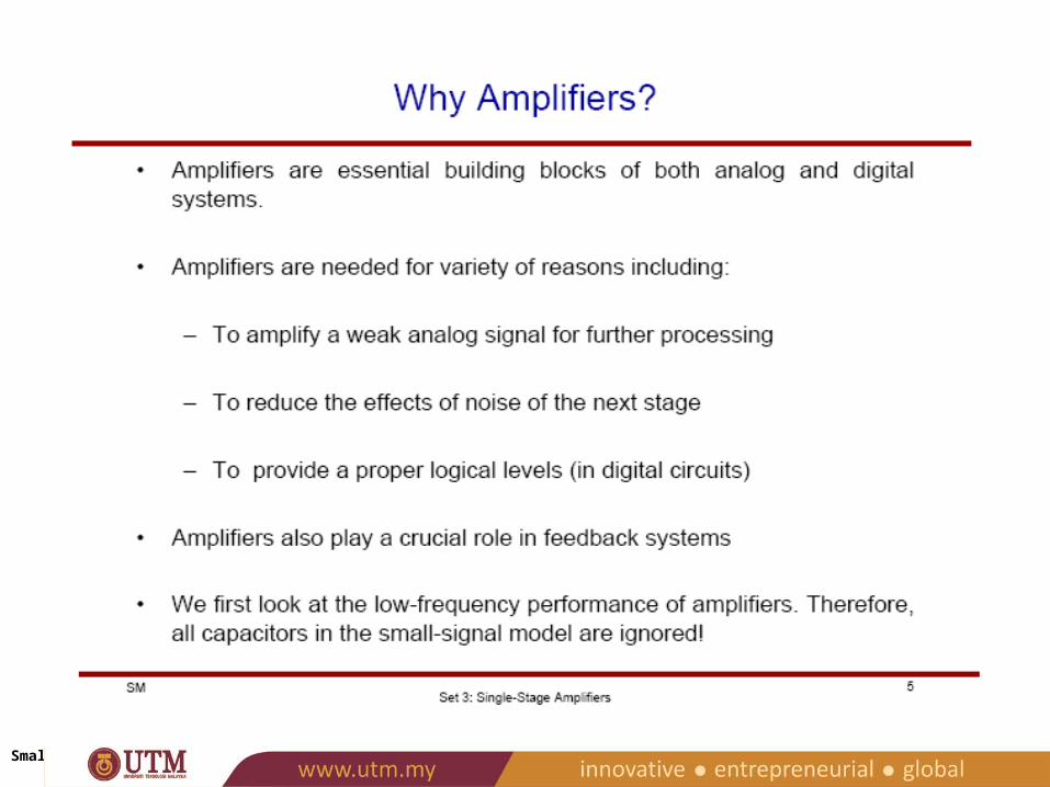
Characterization of AmpLarge signal static characterization
• plot of output versus input (transfer curve)• large signal gain• output and input swing limits
Small signal static characterization• AC gain• AC input resistance• AC output resistance
Small signal dynamic characterization• bandwidth• noise• power supply rejection
Large signal dynamic characterization• slew rate• nonlinearity
When designing amplifier, we need to optimize for some performance parameters.
The parameters trade performance with each other
Single Stage Amplifiers 8
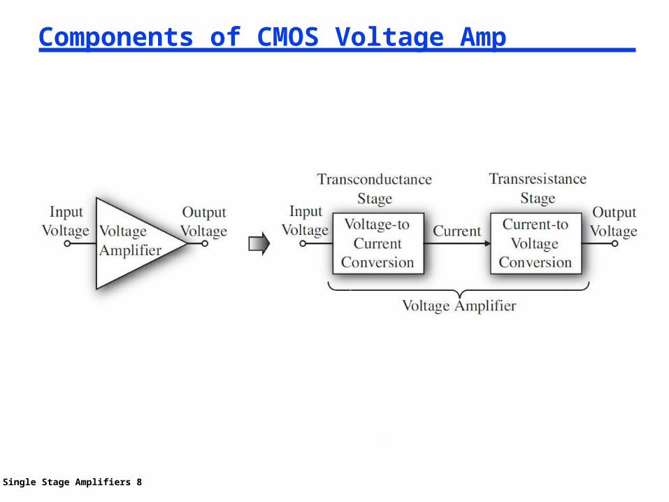
Components of CMOS Voltage Amp
Single Stage Amplifiers 9
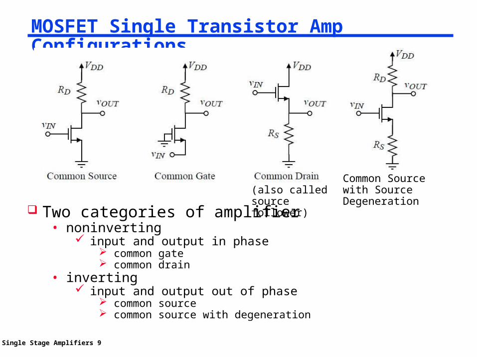
MOSFET Single Transistor Amp Configurations
Two categories of amplifier• noninverting
input and output in phase common gate common drain
• inverting input and output out of phase
common source common source with degeneration
(also called source follower)
Common Source with Source Degeneration

Single Stage Amplifiers 10
Inverter as AmpInverter circuits
• inverters are also common source amps
Single Stage Amplifiers 11
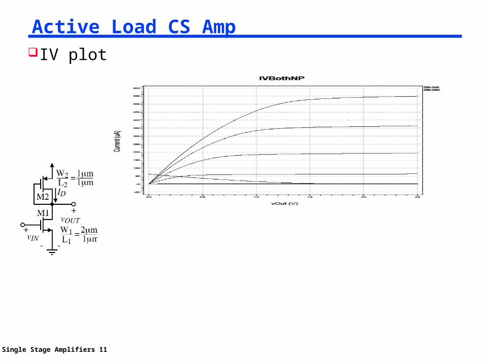
Active Load CS AmpIV plot
Single Stage Amplifiers 12
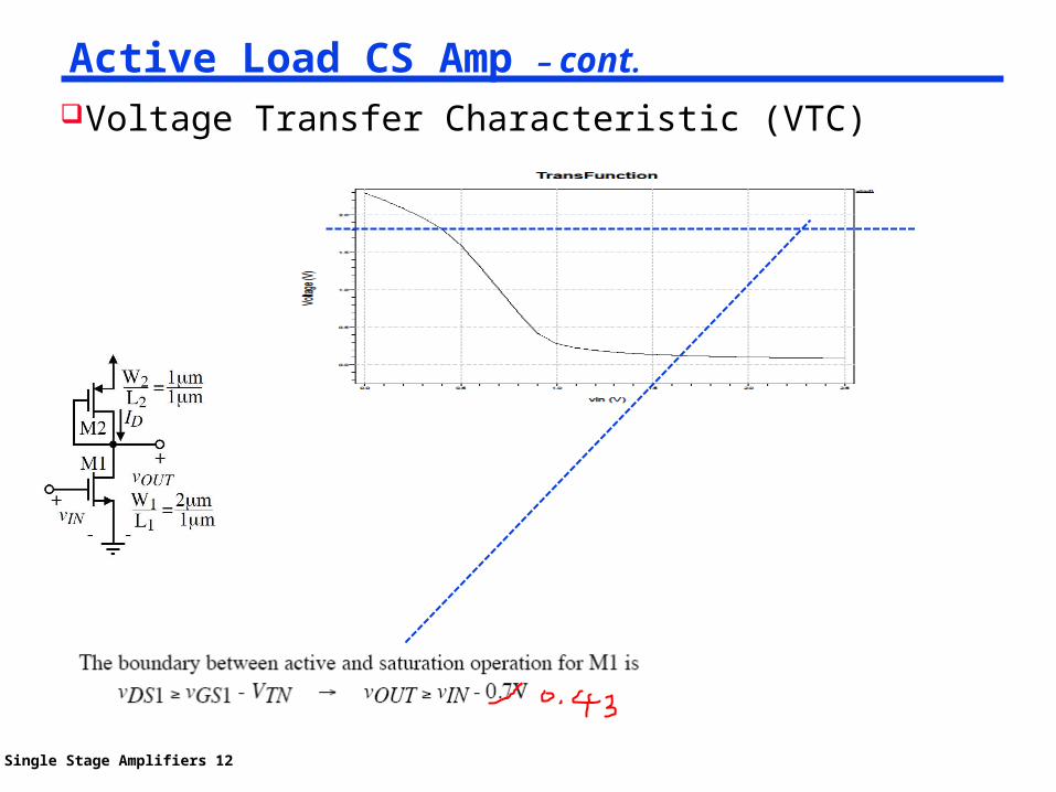
Active Load CS Amp – cont.Voltage Transfer Characteristic (VTC)
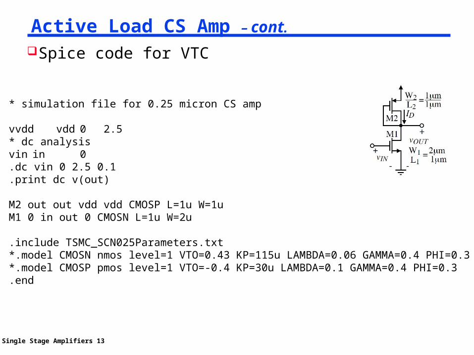
Single Stage Amplifiers 13
Active Load CS Amp – cont.Spice code for VTC
* simulation file for 0.25 micron CS amp
vvdd vdd 0 2.5* dc analysisvin in 0.dc vin 0 2.5 0.1.print dc v(out)
M2 out out vdd vdd CMOSP L=1u W=1uM1 0 in out 0 CMOSN L=1u W=2u
.include TSMC_SCN025Parameters.txt*.model CMOSN nmos level=1 VTO=0.43 KP=115u LAMBDA=0.06 GAMMA=0.4 PHI=0.3*.model CMOSP pmos level=1 VTO=-0.4 KP=30u LAMBDA=0.1 GAMMA=0.4 PHI=0.3.end
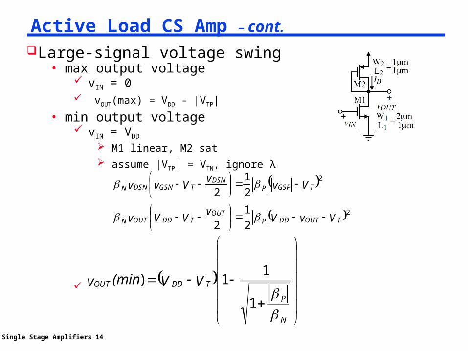
Single Stage Amplifiers 14
Active Load CS Amp – cont.Large-signal voltage swing
• max output voltage vIN = 0 vOUT(max) = VDD - |VTP|
• min output voltage vIN = VDD
M1 linear, M2 sat assume |VTP| = VTN, ignore λ
2
2
21
2
21
2
VvVvVVv
VvvVvv
TOUTDDPOUT
TDDOUTN
TGSPPDSN
TGSNDSNN
N
PTDDOUT VV(minv
1
11)

Single Stage Amplifiers 15
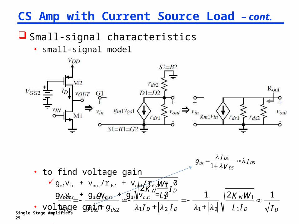
Active Load CS Amp – cont.Small-signal characteristics
• small-signal model assume low-frequency input signal – all
capacitors ignored!
• to find voltage gain gm1vin + vout/rds1 + gm2vout + vout/rds2 = 0
gm1vin + gds1vout + gm2vout + gds2vout = 0• voltage gain
WLKLWK
gg
gggg
vv
P
N
m
m
mdsds
m
in
out
21'
21'
2
1
221
1
ILW
KVILW
Kg DDSDm'' 212
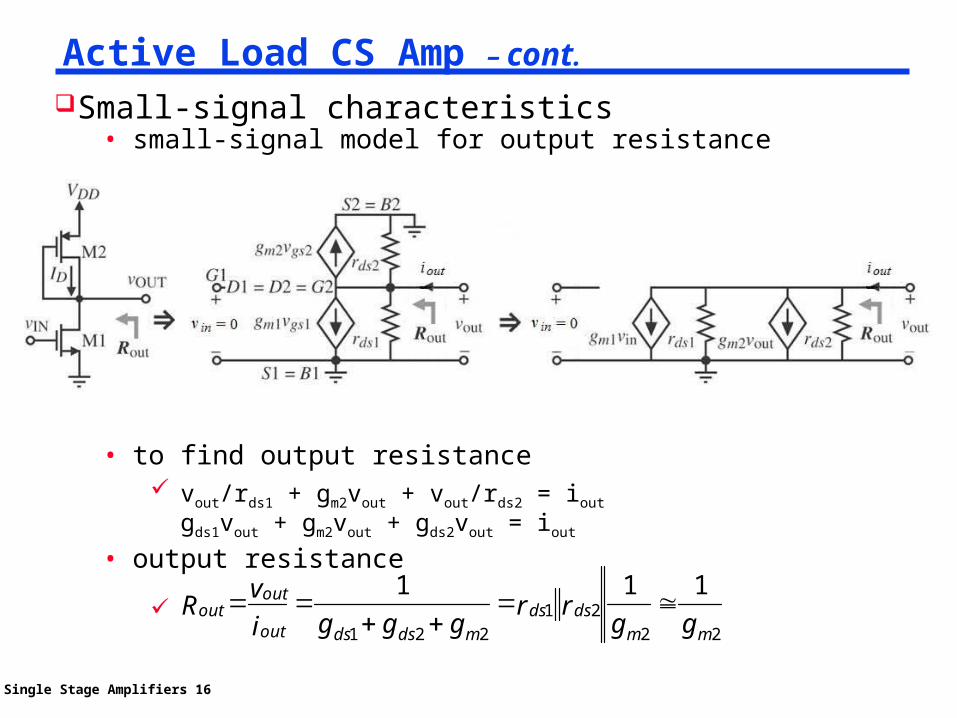
Single Stage Amplifiers 16
Active Load CS Amp – cont.Small-signal characteristics
• small-signal model for output resistance
• to find output resistance vout/rds1 + gm2vout + vout/rds2 = iout
gds1vout + gm2vout + gds2vout = iout
• output resistance ggrrgggi
vRmm
dsdsmdsdsout
outout
2221
221
111
Single Stage Amplifiers 17
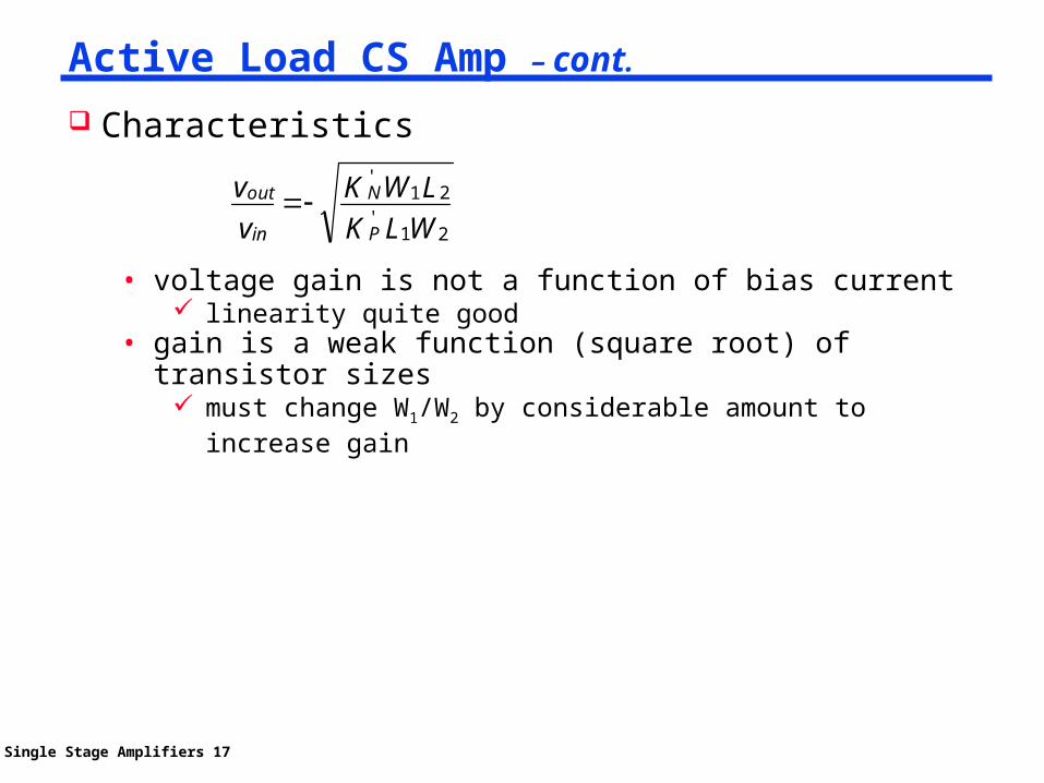
Active Load CS Amp – cont.
Characteristics
• voltage gain is not a function of bias current linearity quite good
• gain is a weak function (square root) of transistor sizes
must change W1/W2 by considerable amount to increase gain
WLKLWK
vv
P
N
in
out
21'
21'

Single Stage Amplifiers 18
Exercise 3-1 For CS amp with resistive load
a) prove that voltage gain vout/vin = -gm1(RL||rds1)b) prove that Rout = RL||rds1c) in terms of linearity, explain why this amp is
worse than active load CS amp
vIN
R L
M 1
VDD
vOUT

Single Stage Amplifiers 19
Exercise 3-2 For diode-connected pMOS circuit
a) prove that input resistance Rin =
b) rederive the voltage gain equation for the active load CS amp by replacing M2 with its equivalent resistance
R in
M 2
VDD
grm
ds2
21
vIN M 1
VDD
vOUT vIN
R L
M 1
VDD
vOUT
M 2
Single Stage Amplifiers 20
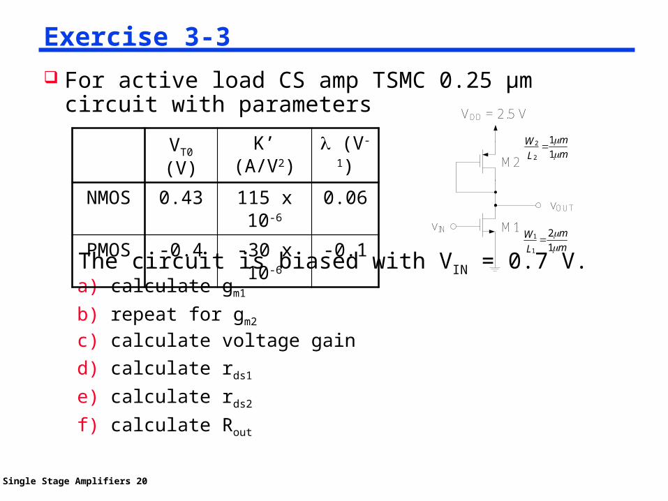
Exercise 3-3 For active load CS amp TSMC 0.25 μm circuit with parameters
The circuit is biased with VIN = 0.7 V.a) calculate gm1
b) repeat for gm2c) calculate voltage gaind) calculate rds1
e) calculate rds2
f) calculate Rout
VT0 (V)
K’ (A/V2)
(V-
1)NMOS 0.43 115 x
10-60.06
PMOS -0.4 -30 x 10-6
-0.1vIN M 1
VDD = 2.5 V
vOUT
M 2
mm
LW
12
1
1
mm
LW
11
2
2
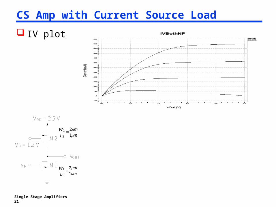
CS Amp with Current Source Load IV plot
vIN M 1
VDD = 2.5 V
vOUT
M 2
mm
LW
12
1
1
mm
LW
12
2
2
VB = 1.2 V
Single Stage Amplifiers 21

CS Amp with Current Source Load – cont.
VTC
vIN M 1
VDD = 2.5 V
vOUT
M 2
mm
LW
12
1
1
mm
LW
12
2
2
VB = 1.2 V
Single Stage Amplifiers 22
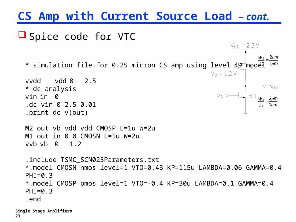
CS Amp with Current Source Load – cont.
Spice code for VTC
vIN M 1
VDD = 2.5 V
vOUT
M 2
mm
LW
12
1
1
mm
LW
12
2
2
VB = 1.2 V* simulation file for 0.25 micron CS amp using level 49 model
vvdd vdd 0 2.5* dc analysisvin in 0.dc vin 0 2.5 0.01.print dc v(out)
M2 out vb vdd vdd CMOSP L=1u W=2uM1 out in 0 0 CMOSN L=1u W=2uvvb vb 0 1.2
.include TSMC_SCN025Parameters.txt*.model CMOSN nmos level=1 VTO=0.43 KP=115u LAMBDA=0.06 GAMMA=0.4 PHI=0.3*.model CMOSP pmos level=1 VTO=-0.4 KP=30u LAMBDA=0.1 GAMMA=0.4 PHI=0.3.end
Single Stage Amplifiers 23
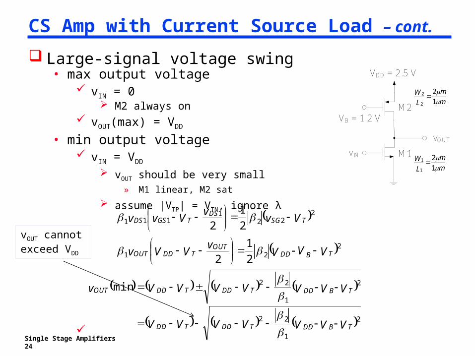
CS Amp with Current Source Load – cont.
Large-signal voltage swing• max output voltage
vIN = 0 M2 always on
vOUT(max) = VDD
• min output voltage vIN = VDD
vOUT should be very small» M1 linear, M2 sat
assume |VTP| = VTN, ignore λ
Single Stage Amplifiers 24
vIN M 1
VDD = 2.5 V
vOUT
M 2
mm
LW
12
1
1
mm
LW
12
2
2
VB = 1.2 V
221
222
1111
21
2
21
2
VVVvVVv
VvvVvv
TDD BOUT
TDDOUT
TSGDS
TGSDS
VVVVVVVv TBDDTDDTDDOUT 2
1
22min
VVVVVVV TBDDTDDTDD 2
1
22
vOUT cannot exceed VDD
CS Amp with Current Source Load – cont.
Small-signal characteristics• small-signal model
• to find voltage gaingm1vin + vout/rds1 + vout/rds2 = 0gm1vin + gds1vout + gds2vout = 0
• voltage gain
Single Stage Amplifiers 25
IILWK
II
ILWK
ggg
vv
DD
N
DD
DN
dsds
m
in
out 1212
1
1'
2121
1
1'
21
1
IVIg DS
DS
DSds
1

CS Amp with Current Source Load – cont.
Small-signal characteristics• small-signal model
• to find output resistance, set vin = 0 gm1vin = 0
• output resistance
Single Stage Amplifiers 26
212121
11
IggrrRDdsds
dsdsout

Exercise 3-4 For CS amp with current source load with TSMC 0.25 μm parameters
The circuit is biased such that the DC voltage for vOUT is 1.3 V.a) calculate the DC value for input vINb) calculate gm1
c) calculate rds1
d) calculate rds2
e) calculate voltage gainf) calculate Rout
Single Stage Amplifiers 27
VT0 (V)
K’ (A/V2)
(V-
1)NMOS 0.43 115 x
10-60.06
PMOS -0.4 -30 x 10-6
-0.1vIN M 1
VDD = 2.5 V
vOUT
M 2
mm
LW
12
1
1
mm
LW
12
2
2
VB = 1.2 V
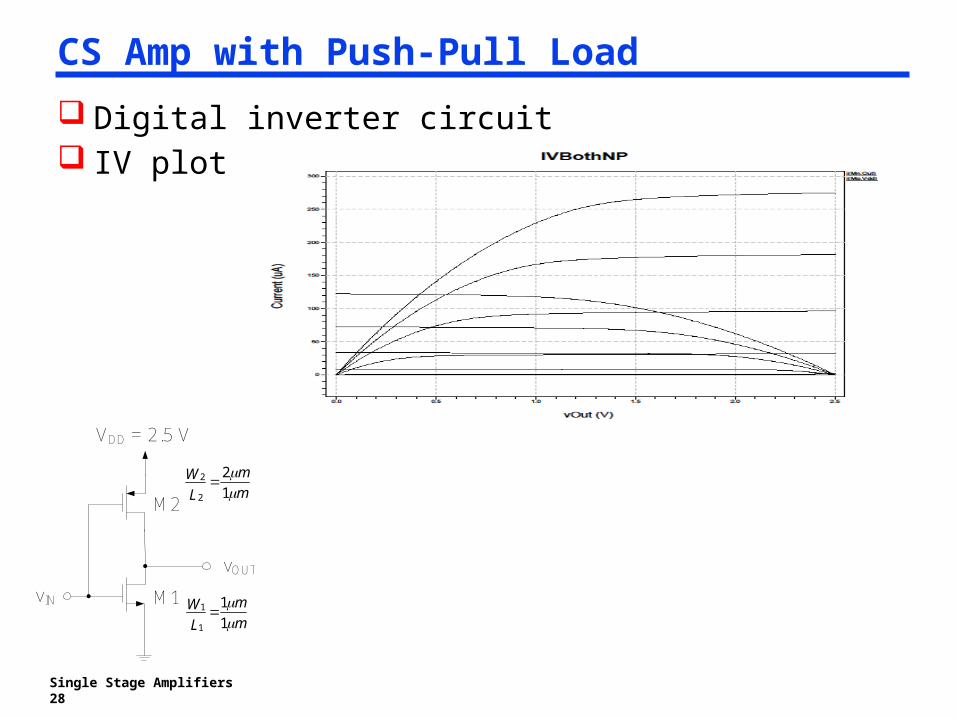
CS Amp with Push-Pull Load Digital inverter circuit IV plot
Single Stage Amplifiers 28
vIN M 1
VDD = 2.5 V
vOUT
M 2 mm
LW
12
2
2
mm
LW
11
1
1

CS Amp with Push-Pull Load – cont.
VTC
Single Stage Amplifiers 29
vIN M 1
VDD = 2.5 V
vOUT
M 2 mm
LW
12
2
2
mm
LW
11
1
1
Level 1 model
Level 49 model

CS Amp with Push-Pull Load – cont.
Spice code for VTC* INVL49 sub-circuit.subckt INVL49 in out vddM2 out in vdd vdd CMOSP L=1u W=2uM1 out in 0 0 CMOSN L=1u W=1u.include TSMC_SCN025Parameters.txt.ends INVL49
* INVL1 sub-circuit.subckt INVL1 in out vddM2 out in vdd vdd CMOSP L=1u W=2uM1 out in 0 0 CMOSN L=1u W=1u.model CMOSN nmos level=1 VTO=0.43 KP=115u LAMBDA=0.06 GAMMA=0.4 PHI=0.3.model CMOSP pmos level=1 VTO=-0.4 KP=30u LAMBDA=0.1 GAMMA=0.4 PHI=0.3.ends INVL1
xL49in outL49 vdd INVL49xL1 in outL1 vdd INVL1
vvddvdd 0 2.5vin in 0.dc vin 0 2.5 0.01.print dc v(outL49) v(outL1).end
Single Stage Amplifiers 30
vIN M 1
VDD = 2.5 V
vOUT
M 2 mm
LW
12
2
2
mm
LW
11
1
1
ports"in out vdd" of INVL1 connected to
"in outL1 vdd" respectively
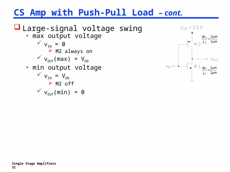
CS Amp with Push-Pull Load – cont.
Large-signal voltage swing• max output voltage
vIN = 0 M2 always on
vOUT(max) = VDD
• min output voltage vIN = VDD
M2 off vOUT(min) = 0
Single Stage Amplifiers 31
vIN M 1
VDD = 2.5 V
vOUT
M 2 mm
LW
12
2
2
mm
LW
11
1
1

CS Amp with Push-Pull Load – cont.
Small-signal characteristics• small-signal model
• to find voltage gaingm1vin + vout/rds1 + gm2vin + vout/rds2 = 0gm1vin + gds1vout + gm2vin + gds2vout = 0
• voltage gain
Single Stage Amplifiers 32
ILWK
LWK
Igggg
vv
D
PN
Ddsds
mm
in
out 1221
2
2'
1
1'
21
21

CS Amp with Push-Pull Load – cont.
Small-signal characteristics• small-signal model
• to find output resistance, set vin = 0 gm1vin = gm2vin = 0
• output resistance
Single Stage Amplifiers 33
212121
11
IggrrRDdsds
dsdsout

Exercise 3-5 For push-pull CS amp with TSMC 0.25 μm parameters
The circuit is biased such that the DC voltage for vOUT is 1.3 V.a) calculate the DC value for input vIN
b) calculate gm1
c) calculate gm2
d) calculate rds1
e) calculate rds2
f) calculate voltage gaing) calculate Rout
Single Stage Amplifiers 34
VT0 (V)
K’ (A/V2)
(V-
1)NMOS 0.43 115 x
10-60.06
PMOS -0.4 -30 x 10-6
-0.1
vIN M 1
VDD = 2.5 V
vOUT
M 2 mm
LW
12
2
2
mm
LW
11
1
1

Summary of CS amps
Single Stage Amplifiers 35
Type AC Voltage Gain Rout
Resistive load -gm1(RL||rds1) RL||rds1
pMOS active load
-gm1/gm2 1/gm2
Current source load
-gm1/(gds1 + gds2) 1/(gds1 + gds2)
Push-pull -(gm1 + gm2)/(gds1 + gds2)
1/(gds1 + gds2)
Single Stage Amplifiers 36
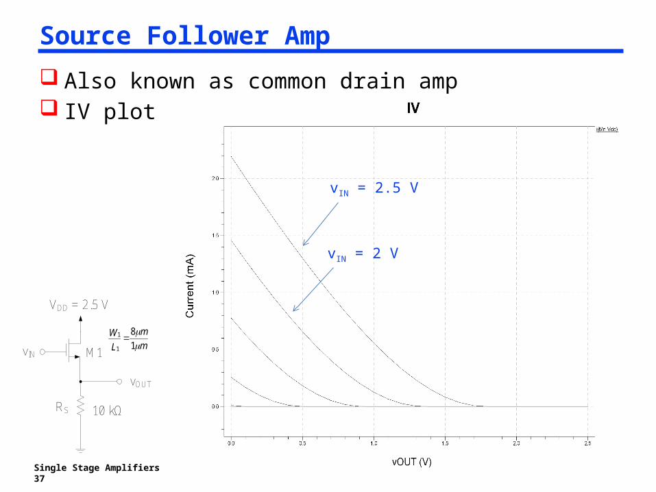
Source Follower Amp Also known as common drain amp IV plot
Single Stage Amplifiers 37
vIN = 2.5 V
vIN = 2 V
vIN M 1
VDD = 2.5 V
vOUTR S 10 kΩ
mm
LW
18
1
1
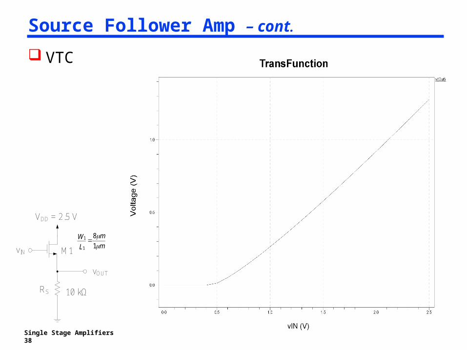
Source Follower Amp – cont.
VTC
Single Stage Amplifiers 38
vIN M 1
VDD = 2.5 V
vOUTR S 10 kΩ
mm
LW
18
1
1
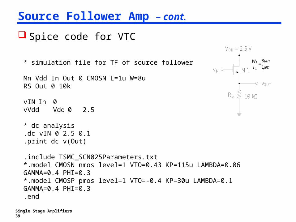
Source Follower Amp – cont.
Spice code for VTC
Single Stage Amplifiers 39
* simulation file for TF of source follower
Mn Vdd In Out 0 CMOSN L=1u W=8uRS Out 0 10k
vIN In 0vVdd Vdd 0 2.5
* dc analysis.dc vIN 0 2.5 0.1.print dc v(Out)
.include TSMC_SCN025Parameters.txt*.model CMOSN nmos level=1 VTO=0.43 KP=115u LAMBDA=0.06 GAMMA=0.4 PHI=0.3*.model CMOSP pmos level=1 VTO=-0.4 KP=30u LAMBDA=0.1 GAMMA=0.4 PHI=0.3.end
vIN M 1
VDD = 2.5 V
vOUTR S 10 kΩ
mm
LW
18
1
1

Source Follower Amp – cont.
Large-signal voltage swing• max output voltage
vIN = VDD VT > VT0 due to body effect! M1 is sat because VDS > VGS – VT
» VDD – vOUT > VDD – vOUT – VT
to find vOUT(max)
for TSMC 0.25 μm tech with KN’ = 115 μA/V2, VT0 = 0.43 V, and ignoring body effect (VT = VT0)
vOUT(max) = 1.5 V for the sample circuit• min output voltage
vIN = 0 M1 off
vOUT(min) = 0Single Stage Amplifiers 40
VvVR
vTOUTDD
S
OUT (max)2(max) 21
vIN M 1
VDD = 2.5 V
vO UTR S 10 kΩ
mm
LW
18
1
1

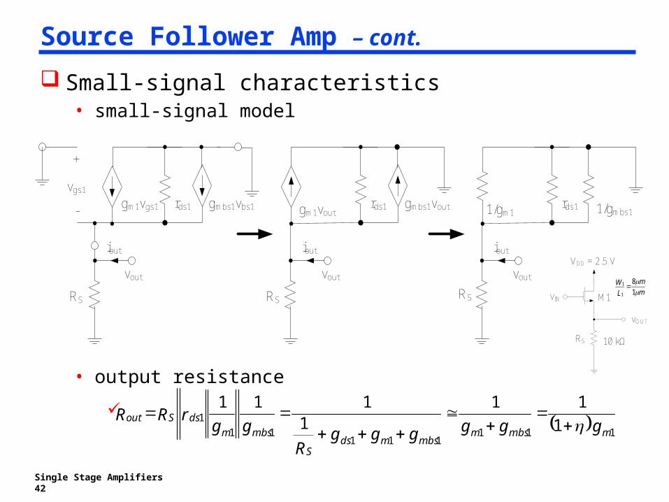
Source Follower Amp – cont. Small-signal characteristics
• small-signal model
• to find voltage gain
• voltage gain
Single Stage Amplifiers 41
gm 1vgs1vgs1
+
- rds1vin
+
-
R S
vout
gm bs1vbs1 gm 1(vin-vout) rds1
R S
vout
gm bs1vout
R S
vout
rds1 1/(gm bs1+gm 1)gm 1vingm 1vin rds1
vout
(gm bs1+gm 1)vout
R S
ggrRvgvmmbs
dsSinmout11
111
111
11
11
1
111
1
1111
ggg
gggR
gggrRg
vv
mbsm
m
mmbsdsS
m
mmbsdsSm
in
out
V
gg
SBF
mmbs
22
vIN M 1
VDD = 2.5 V
vOUTR S 10 kΩ
mm
LW
18
1
1
Source Follower Amp – cont.
Small-signal characteristics• small-signal model
• output resistance
Single Stage Amplifiers 42
gm 1vgs1vgs1
+
- rds1
RS
gm bs1vbs1 gm 1vout rds1
R S
vout
gm bs1vout
vout
iout iout
1/gm 1 rds1
vout
1/gm bs1
iout
R S vIN M 1
VDD = 2.5 V
vO UTR S 10 kΩ
mm
LW
18
1
1
ggggggR
ggrRRmmbsm
mbsmdsS
mbsmdsSout
111111111 1
111
111

Source Follower Amp – cont.
Characteristics
• gain < 1• gain not linear
depends on VOUT since VSB = VOUTcan be resolved by using current sink to bias the source follower
• small output resistance
Single Stage Amplifiers 43
1
111
1gg
gvv
mbsm
m
in
outV SBF
22
gRm
out11
1
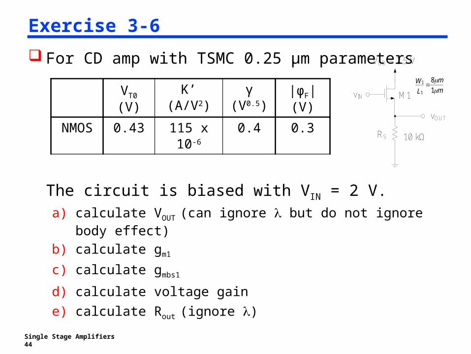
Exercise 3-6 For CD amp with TSMC 0.25 μm parameters
The circuit is biased with VIN = 2 V.a) calculate VOUT (can ignore but do not ignore
body effect)b) calculate gm1
c) calculate gmbs1
d) calculate voltage gaine) calculate Rout (ignore )
Single Stage Amplifiers 44
VT0 (V)
K’ (A/V2)
γ (V0.5)
|φF| (V)
NMOS 0.43 115 x 10-6
0.4 0.3
vIN M 1
VDD = 2.5 V
vOUTR S 10 kΩ
mm
LW
18
1
1
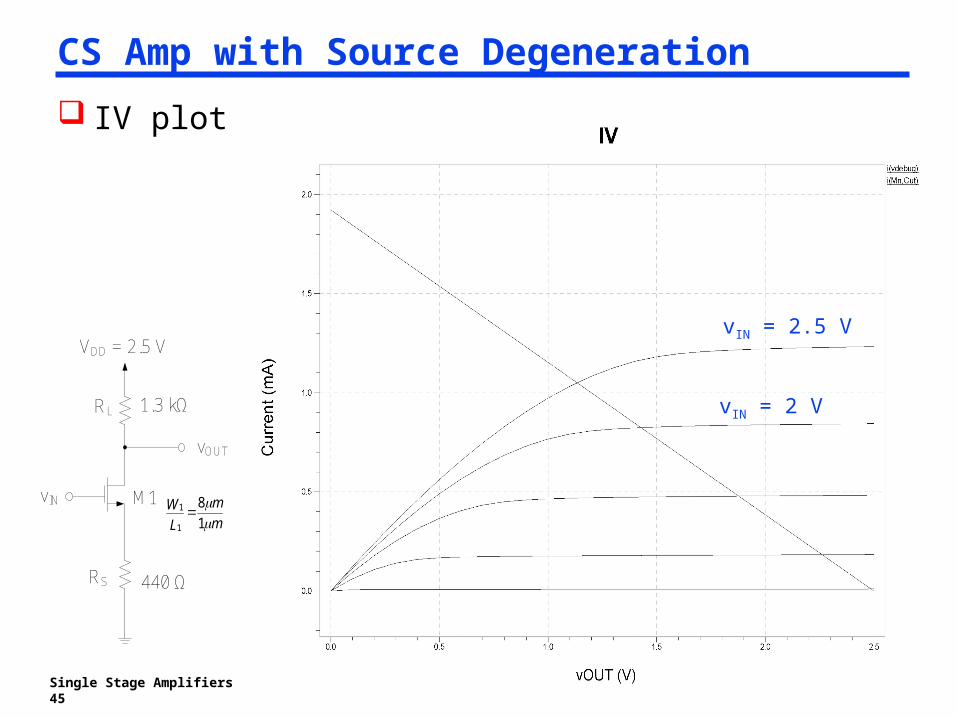
CS Amp with Source Degeneration IV plot
Single Stage Amplifiers 45
vIN = 2.5 V
vIN = 2 V
vIN M 1
VDD = 2.5 V
R S 440 Ω
mm
LW
18
1
1
R L 1.3 kΩ
vOUT

CS Amp with Source Degeneration – cont.
VTC
Single Stage Amplifiers 46
vIN M 1
VDD = 2.5 V
R S 440 Ω
mm
LW
18
1
1
R L 1.3 kΩ
vOUT

CS Amp with Source Degeneration – cont.
Spice code for VTC
Single Stage Amplifiers 47
* simulation file for TF of CS with degenerationMn Out In S 0 CMOSN L=1u W=8uRS S 0 440RL Vdd Out 1.3k
vIN In 0vVdd Vdd 0 2.5
* dc analysis.dc vIN 0 2.5 0.1.print dc v(Out)
*.include TSMC_SCN025Parameters.txt.model CMOSN nmos level=1 VTO=0.43 KP=115u LAMBDA=0.06 GAMMA=0.4 PHI=0.3.model CMOSP pmos level=1 VTO=-0.4 KP=30u LAMBDA=0.1 GAMMA=0.4 PHI=0.3.end
vIN M 1
VDD = 2.5 V
R S 440 Ω
mm
LW
18
1
1
R L 1.3 kΩ
vOUT

CS Amp with Source Degeneration – cont.
Large-signal voltage swing• max output voltage
vIN = 0 M1 off
vOUT(max) = VDD
• min output voltage vIN = VDD
VDS = vOUT – VS VGS – VT = VDD – VT – VS M1 linear if vOUT < VDD – VT
to find vOUT(min)
(1)
(2)
Single Stage Amplifiers 48
RvVRV
L
OUTDDSS
(min)
2(min)(min)(min)
1VvVVVVv
RvV SOUT
TSDDSOUTL
OUTDD
2
(min)(min)1vVVVVv S OUT
TDDSOUT
vIN M 1
VDD = 2.5 V
R S 440 Ω
mm
LW
18
1
1
R L 1.3 kΩ
vOUT
Single Stage Amplifiers 49
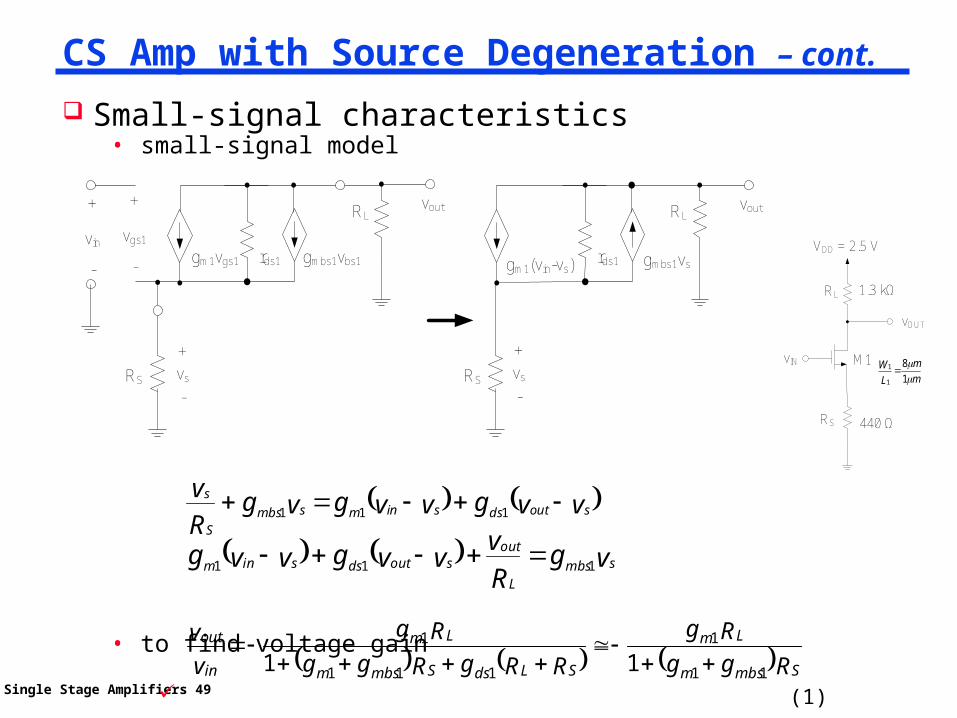
CS Amp with Source Degeneration – cont. Small-signal characteristics
• small-signal model
• to find voltage gain
(1)
(2)
voltage gain
gm 1vgs1vgs1
+
- rds1vin
+
-
R S
gm bs1vbs1 gm 1(vin-vs) rds1
R S
gm bs1vs
R L R Lvout vout
vs+
-vs+
-
vIN M 1
VDD = 2.5 V
R S 440 Ω
mm
LW
18
1
1
R L 1.3 kΩ
vOUT
vvgvvgvgRv
soutdssinmsmbsS
s 111
vgRvvvgvvg smbs
L
outsoutdssinm 111
RggRg
RRgRggRg
vv
Smbsm
Lm
SLdsSmbsm
Lm
in
out
11
1
111
111

CS Amp with Source Degeneration – cont. Small-signal characteristics
• small-signal model
• to find output resistance, 1st find Rx
(1)gds1(vout - vs) = gm1vs + gmbs1vs + ix (2)
Rx = vout/ix = rds1[ 1 + (gm1 + gmbs1 + gds1)RS ] ≈ (gm1 + gmbs1)RSrds1
• output resistance
Single Stage Amplifiers 50
RRrgg
RRrggRRR
LSdsmbsm
LSdsmbsmLxout
111
111
vIN M 1
VDD = 2.5 V
R S 440 Ω
mm
LW
18
1
1
R L 1.3 kΩ
vOUT
gm 1vgs1vgs1
+
- rds1
R S
gm bs1vbs1 gm 1vs rds1
RS
gm bs1vs
R L R Lvout vout
vs+
-vs+
-
iout ioutix
R x
vvgvgvgRv
soutdssmbsmS
ss 111

CS Amp with Source Degeneration – cont.
Characteristics
• if we ignore body effectgain ≈ -gm1RL/(1 + gm1RS)
much more linear, compared to CS amp however, gain is smaller vOUT(min) also much lower
• why more linear?if vIN ↑, ID ↑, voltage across RS ↑, VGS ↓, causing ID ↓
ID less sensitive to input changes
Single Stage Amplifiers 51
RggRg
vv
Smbsm
Lm
in
out
11
11
vIN
R L
M 1
VDD
vOUT
gain = -gm1(RL||rds1)
≈ -gm1RL
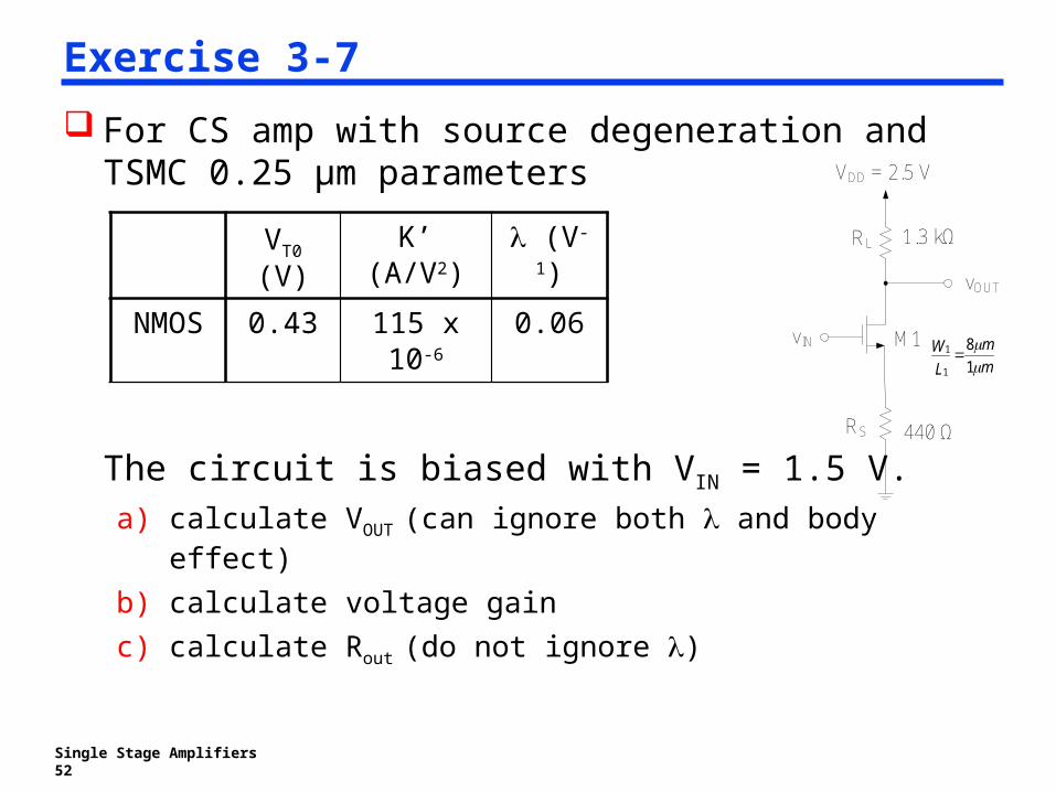
Exercise 3-7 For CS amp with source degeneration and TSMC 0.25 μm parameters
The circuit is biased with VIN = 1.5 V.a) calculate VOUT (can ignore both and body
effect)b) calculate voltage gainc) calculate Rout (do not ignore )
Single Stage Amplifiers 52
VT0 (V)
K’ (A/V2)
(V-
1)NMOS 0.43 115 x
10-60.06 vIN M 1
VDD = 2.5 V
R S 440 Ω
mm
LW
18
1
1
R L 1.3 kΩ
vOUT