EMI Filter Design for a Single-stage Bidirectional and Isolated ...
21
electronics Article EMI Filter Design for a Single-stage Bidirectional and Isolated AC–DC Matrix Converter Diogo Varajão 1,2, * , Rui Esteves Araújo 1,2 , Luís M. Miranda 2 and João A. Peças Lopes 1,2 1 Faculty of Engineering, University of Porto, Rua Doutor Roberto Frias, 4200-465 Porto, Portugal; [email protected] (R.E.A.); [email protected] (J.A.P.L.) 2 INESC TEC—Institute for Systems and Computer Engineering, Technology and Science; Rua Doutor Roberto Frias, 4200-465 Porto, Portugal; [email protected] * Correspondence: [email protected]; Tel.: +351-225-081-808 Received: 17 September 2018; Accepted: 9 November 2018; Published: 12 November 2018 Abstract: This paper describes the design of an electromagnetic interference (EMI) filter for the high-frequency link matrix converter (HFLMC). The proposed method aims to systematize the design process for pre-compliance with CISPR 11 Class B standard in the frequency range 150 kHz to 30 MHz. This approach can be extended to other current source converters which allows time-savings during the project of the filter. Conducted emissions are estimated through extended simulation and take into account the effect of the measurement apparatus. Differential-mode (DM) and common-mode (CM) filtering stages are projected separately and then integrated in a synergistic way in a single PCB to reduce volume and weight. A prototype of the filter was constructed and tested in the laboratory. Experimental results with the characterization of the insertion losses following the CISPR 17 standard are provided. The attenuation capability of the filter was demonstrated in the final part of the paper. Keywords: EMI filter; electromagnetic compatibility; AC–DC power converters; electromagnetic interference filter; matrix converters; current source; power density; battery energy storage systems; battery chargers 1. Introduction Power electronics is making profound changes within the transportation sector [1,2] and the electric power system [3,4]. Bidirectional AC–DC converters are required for several applications, such as battery energy storage systems (BESS) [2,5], chargers for electric vehicles (EVs) [6–8], uninterruptible power supplies (UPS) [9], solid-state transformers (SST) [10], and DC microgrids [11]. The development of new wide bandgap power semiconductors combined with enhanced modulations and control techniques are contributing for the miniaturization and efficiency improvement of the power electronics converters [12]. This is followed by an increase of the switching frequency of the power semiconductors. As a result, conducted emissions (CE) with higher intensity are generated in the measurement range of the electromagnetic compatibility (EMC) standards. In this way, an additional effort is necessary in the design of the electromagnetic interference (EMI) filter included in the input of the power converters in order to comply with the standards [13]. A careful dimensioning of the EMI filter is also essential to ensure the adequate power factor in all operating range and to achieve a high power quality without penalizing the efficiency, volume and cost of the system. Matrix converters (MC) are one of the most interesting families of converters due to its unique and attractive characteristics [14]. By employing an array of controlled four-quadrant power switches, the MC enables AC–AC conversion without any intermediate energy storage element [15]. The high-frequency link matrix converter (HFLMC) is a single-stage bidirectional and isolated AC–DC energy conversion system [16]. The new modulation proposed in [17] and patented in [18] allows Electronics 2018, 7, 318; doi:10.3390/electronics7110318 www.mdpi.com/journal/electronics
-
Upload
khangminh22 -
Category
Documents
-
view
0 -
download
0
Transcript of EMI Filter Design for a Single-stage Bidirectional and Isolated ...

electronics
Article
EMI Filter Design for a Single-stage Bidirectional andIsolated AC–DC Matrix Converter
Diogo Varajão 1,2,* , Rui Esteves Araújo 1,2 , Luís M. Miranda 2 and João A. Peças Lopes 1,2
1 Faculty of Engineering, University of Porto, Rua Doutor Roberto Frias, 4200-465 Porto, Portugal;[email protected] (R.E.A.); [email protected] (J.A.P.L.)
2 INESC TEC—Institute for Systems and Computer Engineering, Technology and Science;Rua Doutor Roberto Frias, 4200-465 Porto, Portugal; [email protected]
* Correspondence: [email protected]; Tel.: +351-225-081-808
Received: 17 September 2018; Accepted: 9 November 2018; Published: 12 November 2018
Abstract: This paper describes the design of an electromagnetic interference (EMI) filter for thehigh-frequency link matrix converter (HFLMC). The proposed method aims to systematize the designprocess for pre-compliance with CISPR 11 Class B standard in the frequency range 150 kHz to 30 MHz.This approach can be extended to other current source converters which allows time-savings duringthe project of the filter. Conducted emissions are estimated through extended simulation and takeinto account the effect of the measurement apparatus. Differential-mode (DM) and common-mode(CM) filtering stages are projected separately and then integrated in a synergistic way in a single PCBto reduce volume and weight. A prototype of the filter was constructed and tested in the laboratory.Experimental results with the characterization of the insertion losses following the CISPR 17 standardare provided. The attenuation capability of the filter was demonstrated in the final part of the paper.
Keywords: EMI filter; electromagnetic compatibility; AC–DC power converters; electromagneticinterference filter; matrix converters; current source; power density; battery energy storage systems;battery chargers
1. Introduction
Power electronics is making profound changes within the transportation sector [1,2] and theelectric power system [3,4]. Bidirectional AC–DC converters are required for several applications,such as battery energy storage systems (BESS) [2,5], chargers for electric vehicles (EVs) [6–8],uninterruptible power supplies (UPS) [9], solid-state transformers (SST) [10], and DC microgrids [11].The development of new wide bandgap power semiconductors combined with enhanced modulationsand control techniques are contributing for the miniaturization and efficiency improvement of thepower electronics converters [12]. This is followed by an increase of the switching frequency of thepower semiconductors. As a result, conducted emissions (CE) with higher intensity are generated in themeasurement range of the electromagnetic compatibility (EMC) standards. In this way, an additionaleffort is necessary in the design of the electromagnetic interference (EMI) filter included in the input ofthe power converters in order to comply with the standards [13]. A careful dimensioning of the EMIfilter is also essential to ensure the adequate power factor in all operating range and to achieve a highpower quality without penalizing the efficiency, volume and cost of the system.
Matrix converters (MC) are one of the most interesting families of converters due to its uniqueand attractive characteristics [14]. By employing an array of controlled four-quadrant powerswitches, the MC enables AC–AC conversion without any intermediate energy storage element [15].The high-frequency link matrix converter (HFLMC) is a single-stage bidirectional and isolated AC–DCenergy conversion system [16]. The new modulation proposed in [17] and patented in [18] allows
Electronics 2018, 7, 318; doi:10.3390/electronics7110318 www.mdpi.com/journal/electronics

Electronics 2018, 7, 318 2 of 21
independent control of active and reactive power (PQ control) as well as the DC current in thebattery pack. By exploring the MC attributes, circuit volume and weight can be reduced, and a longerservice life is expected when compared with equivalent DC-link based solutions [16,19,20]. However,due to its complex power structure, it presents EMC challenges that have to be studied in order toensure compliance with the international standards by designing the necessary EMI filter.
Several approaches for the design of differential-mode (DM) and common-mode (CM) filteringstages for direct and indirect matrix converters (MC) were proposed in [20–33]. However, in spite of thelong history of this question, until now there has been no complete systematization regarding whichtopologies and damping methods should be used for each DM and CM filtering stage. Among theseworks, there are also some procedures of design and formulas that simply do not match betweendifferent papers, which may mislead or confuse the reader. Additionally, these works do not show thecomplete design process from the requirements specification until the experimental characterization ofthe insertion losses. According to our best knowledge, this is the first work in literature that proposea complete design of EMI filter for the HFLMC. The main contribution of this paper is setting upa systematic methodology for the design process of the HFLMC’s EMI filter for CISPR 11 ClassB pre-compliance. This design process also takes into account the modeling of the measurementequipment, such as the Line Impedance Stabilizing Network (LISN) and the Test Receiver (TR),in order to better predict the effectiveness of the designed EMI filter. Furthermore, a practical way tocharacterize the insertion losses according the CISPR 17 standard is fully described and supported byexperimental results. It is worth noting that this is the same procedure followed by the manufacturersto characterize their EMI filters. In addition, this is the typical information available in the EMI filterdatasheet and is very useful to compare the effectiveness of different filters.
The manuscript is organized as follows: the HFLMC is briefly presented in Section 2. Then,the applicable standards and the measurement approach of CE are described in Section 3. The detaileddesign of DM and CM filtering stages is explained in Sections 4 and 5, respectively. Section 6 presentsthe proposed integration strategy of the different filtering stages. The experimental results are shownin Section 7. Finally, Section 8 draws conclusions and proposes future work.
2. High-Frequency Link Matrix Converter
Figure 1 shows the HFLMC proposed for single-stage bidirectional and isolated AC–DC energyconversion. Each bidirectional switch Sxy is composed of two transistors: Sxy1 and Sxy2 (x = a, b, cand y = P, N) in a common-source configuration. Command signals for the power semiconductorsare generated by the modulation proposed in [17] and patented in [18]. The MC applies voltage vp
to the high-frequency transformer (HFT) [34]. The full-bridge produces io by impressing vs in theHFT secondary. Finally, the output filter reduces the ripple in the DC current iDC that charges anddischarges the battery pack.

Electronics 2018, 7, 318 3 of 21
Input Filter Three-phase to Single-phase Matrix ConverterHigh-frequency
TransformerFull-Bridge Output Filter
Battery
Pack
iL L
Co
io
va
vb
vc
vga
vgb
vgc
CF
ia
ic
ib
Grid
Lo idcSaP2
SaP1
SbP2
SbP1
ScP2
ScP1
SaN1
SaN2
SbN1
SbN2
ScN1
ScN2
vp vs vo
S4 S2
S3S1
vdc
n : 1
iga
igb
igc
P
N
EMI
Filter
Figure 1. Circuit schematic of the high-frequency link matrix converter.
The EMI filter is projected to attenuate the noise present on currents ia,b,c generated by thethree-phase to single-phase matrix converter. For this reason, the matrix converter side is consideredthe input of the filter and the grid side the output. It is expected that the conducted noise existent incurrents iga,b,c be within the limits specified in the international standards.
3. Standards and CE Measurement
The CE are generated by harmonics present in the input current of the MC, ii = [ia, ib, ic], whereia, ib and ic are the phase currents. EMC standards classify the CE according to the frequencyrange [35]. Low-frequency harmonics are typically measured up to 2 kHz (40th harmonic) asdefined by IEC 61000-3-2 [36]. Section 6 presents the low-frequency (LF) harmonics measured forthis converter and compared with IEC 61000-3-2 Class A limits. Regarding the HF conducted emissions,CISPR 11 [37] specifies the limits for frequencies from 150 kHz to 30 MHz. These emissions canbe estimated by simulating the converter operation without any input filter at nominal conditions:Pnom = 10 kW, line-to-neutral grid voltage Vg,ln = 230 V, grid frequency fg = 50 Hz and outputvoltage VDC = 380 V. A simulation model of the HFLMC was implemented in GeckoCIRCUITS (v1.7.2Professional, Gecko-Simulations A.G., Dübendorf, Switzerland) [38]. This software has a measure blockthat performs analysis according to the CISPR 16 [39] standard using the time domain simulation data.Similar to a test receiver (TR), it is possible to select different signal processing options: average (AVG),quasi-peak (QP) or peak detection. The first step of the filter design is to specify the maximumadmissible CE levels. Due to the type of application, the QP limits of the CISPR 11 Class B curvewill be considered. A line impedance stabilizing network (LISN) is connected between the grid andthe device under test (DUT) in order to provide a known impedance and ensure the reproducibilityof the measurements [40]. Then, a TR calculates the CE in "dBµV" through the measurement of thevoltage at the LISN output port, VTR. An equivalent impedance of 50 Ω/50µH is specified by the CISPR16 standard for the TR/LISN. The LISN’s transfer function from VTR to DUT’s input current is [41]:
GLISN(s) =VTR(s)Idut(s)
=s2LLISNCLISN RTR
s2LLISNCLISN + sRTRCLISN + 1, (1)
where RTR = 50 Ω, LLISN = 50 µH and CLISN = 250 nF.
4. Design of Differential-Mode Filter
4.1. Spectrum of the Converter Input Current
Due to the symmetry of the converter and the measurement system, the DM input filter can beprojected considering a single-phase equivalent circuit [27]. Figure 2a shows the spectrum of the input

Electronics 2018, 7, 318 4 of 21
current of one phase, Idm(jω), obtained from simulation. Since no circuit element is connected betweenthe lines and the ground (PE), only DM current is present at Idut(s). As can be seen, the first significantharmonic content appears around the switching frequency, fs = 20 kHz. Other harmonics are alsopresent at frequencies multiple of fs. The first switching frequency harmonic inside the measurementrange appears at 160 kHz. A zoom around this frequency is depicted in Figure 2b.
(a) (b)
Figure 2. (a) frequency spectrum of the converter input current Idm(jω); (b) zoom around the firstswitching frequency harmonic above 150 kHz.
4.2. Spectrum of the Measured Voltage
The spectrum of VTR can be determined by the multiplication of Idm(jω) with Equation (1).Figure 3 depicts the spectrum of VTR(jω) at the LISN’s output terminals along with the maximumand minimum estimation of the CE levels using QP detection. The exact QP values will be betweenthe MaxTR and MinTR curves. Further details about the modeling of the TR and the determinationprocess of these curves are described in [23].
MaxTR(jω)MinTR(jω)
VTR(jω)
Figure 3. TR measurement without the DM filter: maximum and minimum estimation of CE alongwith the spectrum of VTR(jω).
4.3. Required Attenuation
The required attenuation for the DM filter can be estimated without the need for calculating theexact QP values. The predicted CE level at 160 kHz by MaxTR curve is 182.9 dBµV. By analysing thiscurve, the next switching frequency harmonic appears at 180 kHz and requires lower attenuation.Thus, the filter design will focus on the emissions at 160 kHz. The limit specified at this frequencyby CISPR 11 is LimitCISPR,160kHz = 65.5 dBµV. A margin of 6 dB is added in order to account forpossible inaccuracies in CE estimation, and also for the parasitics of the inductive and capacitive
Electronics 2018, 7, 318 5 of 21
components [41]. In this way, the design process can be faster since the parasitic effects are notconsidered in the first step. Finally, the required attenuation of the DM filter at 160 kHz is:
Attreq,DM =MaxTR,160kHz − LimitCISPR,160kHz + Margin = 123.4 dB. (2)
4.4. Topology
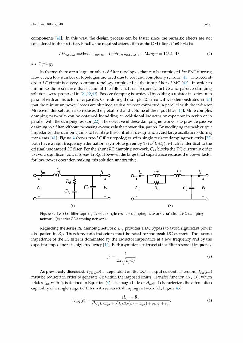
In theory, there are a large number of filter topologies that can be employed for EMI filtering.However, a low number of topologies are used due to cost and complexity reasons [41]. The second-order LC circuit is a very common topology employed as the input filter of MC [42]. In order tominimize the resonance that occurs at the filter, natural frequency, active and passive dampingsolutions were proposed in [21,22,43]. Passive damping is achieved by adding a resistor in series or inparallel with an inductor or capacitor. Considering the simple LC circuit, it was demonstrated in [25]that the minimum power losses are obtained with a resistor connected in parallel with the inductor.Moreover, this solution also reduces the global cost and volume of the input filter [14]. More complexdamping networks can be obtained by adding an additional inductor or capacitor in series or inparallel with the damping resistor [22]. The objective of these damping networks is to provide passivedamping to a filter without increasing excessively the power dissipation. By modifying the peak outputimpedance, this damping aims to facilitate the controller design and avoid large oscillations duringtransients [41]. Figure 4 shows two LC filter topologies with single resistor damping networks [22].Both have a high frequency attenuation asymptote given by 1/(ω2L f C f ), which is identical to theoriginal undamped LC filter. For the shunt RC damping network, C f d blocks the DC current in orderto avoid significant power losses in Rd. However, the large total capacitance reduces the power factorfor low-power operation making this solution unattractive.
L1d
A1
B1
C1
L3
C3R1d
L1
C1
A1
B1
C1
LISN
idm
L1d
L3 C3
L1
C1R1d
L2d
R2d
L2
C2
L2d L2
C2R2d
Lfd Lf
CfRd
Lf
Cf
Rd
Cfd
Lfd Lf
CfRd
Lf
Cf
Rd
Cfd
imim iiii
imim iiii
vmvm vivi
vivivmvm
(a)
L1d
A1
B1
C1
L3
C3R1d
L1
C1
A1
B1
C1
LISN
idm
L1d
L3 C3
L1
C1R1d
L2d
R2d
L2
C2
L2d L2
C2R2d
Lfd Lf
CfRd
Lf
Cf
Rd
Cfd
Lfd Lf
CfRd
Lf
Cf
Rd
Cfd
imim iiii
imim iiii
vmvm vivi
vivivmvm
(b)
Figure 4. Two LC filter topologies with single resistor damping networks. (a) shunt RC dampingnetwork; (b) series RL damping network.
Regarding the series RL damping network, L f d provides a DC bypass to avoid significant powerdissipation in Rd. Therefore, both inductors must be rated for the peak DC current. The outputimpedance of the LC filter is dominated by the inductor impedance at a low frequency and by thecapacitor impedance at a high frequency [44]. Both asymptotes intersect at the filter resonant frequency:
f0 =1
2π√
L f C f
. (3)
As previously discussed, VTR(jω) is dependent on the DUT’s input current. Therefore, Idm(jω)
must be reduced in order to generate CE within the imposed limits. Transfer function Hlcrl(s), whichrelates Idm with Ii, is defined in Equation (4). The magnitude of Hlcrl(s) characterizes the attenuationcapability of a single-stage LC filter with series RL damping network (cf., Figure 4b):
Hlcrl(s) =sL f d + Rd
s3C f L f L f d + s2C f Rd(L f + L f d) + sL f d + Rd. (4)

Electronics 2018, 7, 318 6 of 21
A compromise between damping and the size of L f d must be done during the design process [44].The damping ratio nd defines the relation between inductor L f d and L f . For practical purposes,a unitary damping ratio is interesting since only one type of inductor needs to be built/purchased.According to [41], this solution also results in acceptable losses on Rd. As demonstrated in [22],the optimum damping resistance for the series RL damping network can be calculated as:
Rd =
√L f
C f
1 + ndnd
√2(1 + nd)(4 + nd)
(2 + nd)(4 + 3nd). (5)
Figure 5 shows the impact of different damping factors in terms of resonance of Hlcrl(s) forC f = 20 µF and L f = 60 µH. As expected, the peak in the magnitude is reduced when the damping isincreased. Simultaneously, the frequency at which this peak occurs also decreases as damping rises.Nevertheless, the low and high frequency asymptotes are not affected by the damping factor.
nd = 0.1
nd = 0.25
nd = 0.5
nd = 1
Figure 5. Impact of different damping factors in transfer function Hlcrl(s).
For a given attenuation, the cascade connection of multiple LC filter stages allows the reductionof volume and weight when compared to a single-stage LC filter [44]. This is achieved by increasingthe cutoff frequencies of the multiple stages resulting in smaller inductance and capacitance values.Nevertheless, the interaction between cascaded LC filter stages can provoke additional resonances andincreased output impedance. An approach to reduce this interaction is by selecting gradually smallercutoff frequencies as it nears the filter output [22]. In other words, higher attenuation is required forthe stages near the filter output to improve system stability.
4.5. Components
In order to provide the required attenuation, a three-stage filter as shown in Figure 6 is employed.Stage 1 and Stage 2 are formed by LC filters with series RL damping networks, and Stage 3 is anundamped LC filter formed by C3 and L3.
idm
L1d
L3 C3
L1
C1R1d
L2d L2
C2R2d
Figure 6. Equivalent single-phase circuit of the DM filter.
The DM capacitors draw reactive current from the grid, which decreases the operating powerfactor (PF). In order to have a minimum power factor during a light load operation, the total capacitancemust be limited to the converter nominal power. In [45], the authors suggest that the PF must be atleast 0.9 for operation at 10% of Pnom. Other authors consider that a 0.8 power factor for the same

Electronics 2018, 7, 318 7 of 21
operating conditions is reasonable [28]. The capacitance limitation can also be specified in terms ofthe absolute value for the reactive power. For instance, in [20], it is proposed that the reactive powerdrawn by the input filter must be restricted to 15% of Pnom. Assuming a small voltage drop for thefundamental component across the filter inductors, the total reactive power absorbed can be calculatedby Equation (6). Considering this last criteria, the maximum capacitance per phase must be restrictedto C f ,total ≤ 30µF:
QC f ≈ 3 · 2π · fg · C f ,total ·V2g,ln. (6)
4.5.1. Stage 1
The matrix converter is a voltage-fed topology and behaves as a current source at its input.Capacitor C1 (CF in Figure 1) is placed at the MC input in order to limit the voltage ripple and ensurea correct system operation. For the worst operations conditions, the peak current at the MC input isIi = 37 A. By defining δvC f ,pp as the maximum peak-to-peak voltage ripple, the minimum requiredcapacitance can be calculated as [46]:
C1 ≥Ii
1.1 ·Vg,ln · 2π · fs · δvC f ,pp. (7)
By limiting δvC f ,pp to about 5–10% of the nominal input voltage [41,46], the minimum requiredcapacitance must be between 11.6 and 23.2 µF. Due to the discrete availability of capacitance valuesand also for practical implementation reasons, capacitor C1 is selected to 20 µF.
The magnitude of the LF current harmonics can be affected if the resonant frequency ( f0) of thedifferent filter stages is near the measurement range (up to 2 kHz). However, the resonant frequencymust be significantly lower than the switching frequency in order to provide sufficient attenuation atf = fs. Therefore, it is common to choose a resonant frequency between 20 times the grid frequency andabout one-third of the switching frequency [26]. Considering this criteria, the resonant frequency forStage 1 must be between 1 and 6.66 kHz. As previously discussed, the attenuation for this stage mustbe higher than the other stages, resulting in a lower resonant frequency for Stage 1 when compared toStage 2. The attenuation for Stage 1 is selected as AttStage1 = 0.5 · Attreq,DM, which by the following:
f0,Stage1 =160kHz√10
AttStage120
(8)
results in f0,Stage1 = 4588 Hz. Considering C1 and Equation (3), L1 is calculated as 60 µH. For n1d = 1,the damping network is composed by L1d = 60µH and R1d = 3.4 Ω according to Equation (5).
4.5.2. Stage 2
For practical reasons, L2 and L2d are selected to be equal to L1 and L1d. By defining AttStage2 =
0.35 · Attreq,DM, the resonant frequency of Stage 2 needs to be f0,Stage2 = 13316 Hz. Considering L2
and Equation (3), C2 is calculated as 2.3 µF. Due to the discrete availability of capacitance values, C2 isselected to be 2.2 µF. Finally, the unitary damping ratio results in R2d = 10 Ω.
4.5.3. Stage 3
The third stage of the filter is composed by C3 in combination with L3. During test experiments,L3 corresponds to the inner inductance of the LISN, LLISN . For normal operation, L3 coincideswith the grid inductance, Lg. Although the grid inductance can vary significantly depending ofthe PCC, for this analysis, Lg = 50 µH is considered, following the reference network defined inIEC 61000-3-3 [47]. This stage must provide the remainder attenuation, which can be written asAttStage3 = Attreq,DM − AttStage1 − AttStage2. Therefore, the resonant frequency of Stage 3 needs to bef0,Stage3 = 53204 Hz. Considering L3 = 50 µH, the respective capacitor is chosen to be C3 = 180 nF.

Electronics 2018, 7, 318 8 of 21
4.6. Evaluation of the DM Filter
By combining all three stages, the complete transfer function Hdm from Ii to Idm can be obtained.Figure 7 depicts the frequency response of the DM filter. As required, a 123 dB attenuation is providedat 160 kHz. The effect of the damping networks is perceptible by comparing the gain at f0,Stage1 andf0,Stage2 with the gain at f0,Stage3.
−123dB
fs
Figure 7. Frequency response of the DM filter: magnitude of Hdm, the transfer function from Ii to Idm.
Figure 8 depicts MaxTR and MinTR for the converter operation with the DM filter. As can be seen,the maximum curve for the predicted QP values is below the limits specified by the CISPR 11 Class Bcurve and the selected margin of 6 dB can be observed. Thus, the DM filter design is considered tobe concluded.
Figure 8. TR measurement with DM filter: maximum and minimum estimation of CE.
5. Design of the Common-Mode Filter
5.1. Common-Mode Voltage
The CM voltage generated by the matrix converter induces a circulating current, icm, throughthe converter and the ground (see Figure 9). This current closes the loop through the TR/LISNimpedance resulting in CE that must be within the limits specified by CISPR 11. Silicon Carbide (SiC)MOSFET C2M0025120D is used for the converter implementation. The parasitic capacitance from thesemiconductor to the heat sink per unit area is approximated by 20 pF/cm2 [32]. Considering thisreference value, the parasitic capacitance of all the matrix converter’s semiconductors is Cgh = 600 pF.Regarding the transformer interwinding capacitance and the stray primary side wiring capacitance, it isdifficult to estimate these values without making measurements. For this reason, a 1.2 nF capacitanceis added to the simulated circuit in order to take into account these parasitics. Thus, a total parasitic

Electronics 2018, 7, 318 9 of 21
capacitance to ground Cg = 1.8 nF is considered. The resulting CM voltage, vcm, impressed by the MCis represented in Figure 9. This voltage has approximately 110 Vrms and a peak equal to Vg,ln.
-300
-200
-100
0
100
200
300
Voltage(V
)
80 90 100 110 120
Time (ms)
vcm
Figure 9. Common-mode voltage impressed by the matrix converter.
The frequency spectrum of the simulated RMS common-mode current (icm(jω)) for this operatingpoint is shown in Figure 10. A zoom around the first switching harmonic inside the measurementrange is shown in Figure 10b.
(a) (b)
Figure 10. (a) frequency spectrum of the common-mode current Icm(jω); (b) zoom around the firstswitching frequency harmonic above 150 kHz.
5.2. Spectrum of the Measured Voltage
The converter and the measurement system can be reduced to its single-phase equivalent CMcircuit as represented in Figure 11. It is important to note that, from the CM point of view, the threeline-to-ground capacitors of each stage are in parallel. Thus, the effective common-mode capacitance isequal to the sum of the three capacitor values [48]. The LISN and the TR are modeled by its equivalentCM impedance. vcm is modeled by an ideal voltage source.
PE
Ccm2 Ccm1
Lcm2
Ccm2
Lcm1
Ccm1
vcm
CgZLISN/3
icm
Figure 11. Equivalent single-phase circuit of the CM filter.

Electronics 2018, 7, 318 10 of 21
The Cg connected to the ground represents the parasitic capacitance. The spectrum of VTR can bedetermined by the multiplication of Icm(jω) with the LISN’s transfer function GLISN,CM = GLISN/3.Figure 12 depicts the spectrum of VTR at the LISN output terminals along with the MaxTR and MinTRusing QP detection.
MaxTR(jω)
MinTR(jω)
VTR(jω)
Figure 12. TR measurement without CM filter: maximum and minimum estimation of CE along withthe spectrum of VTR(jω).
5.3. Required Attenuation
The required attenuation for the CM filter can be estimated without the need of calculating theexact QP values. The predicted CE at 160 kHz by MaxTR(jω) curve is 123.7 dBµV. The limits specifiedin the CISPR 11 Class B for CM are equal to the DM. Considering the limit at 160 kHz and including amargin of 6 dB, the required attenuation of the CM filter at 160 kHz is Attreq,CM = 64.2 dBµV.
5.4. Topology
In order to limit icm, the EMI filter must maximize the mismatch between the power source andthe converter impedances [49]. LC circuits are usually employed for the common-mode filter [50].In contrast with the DM filter, no additional damping needs to be added by external elements.The CM inductors are connected in series with the lines in order to provide a high-impedance for thecommon-mode noise. The three windings of the inductor are wound on the same core, which forms acommon-mode choke. Because the power line currents are symmetrically displaced in each winding,the magnetic flux produced in the core by these currents cancels.
5.5. Components
In order to provide the required attenuation a two-stage CM filter is employed (see Figure 11).Stage 1 and Stage 2 are formed by undamped LC filters that make the connection between the linesand the ground (PE). The maximum value of the line-to-ground capacitance is limited by the leakagerequirements imposed by several safety agencies [48]. This safety measure is necessary for protectionof personnel against electric shock under fault conditions.
According to IEC 60950, the ground leakage current for Class I equipment must be limitedto Ileak,max = 3.5 mA at 50 Hz. This requirement has a great impact on the CM filter design.Considering the upper limit of the grid RMS voltage, a maximum total CM capacitance per phase ofCcm,max = 44 nF is calculated by:
Ccm,max =Ileak,max
1.1 ·Vg,ln · 2π · fg. (9)

Electronics 2018, 7, 318 11 of 21
According to [41], for maximum attenuation given a minimum total capacitance, each stageshall present the same value. In order to provide some margin to the imposed limit of Ccm,max,a total capacitance per phase of 20 nF is chosen. Therefore, capacitors Ccm1 and Ccm2 must be 10 nF.Considering this capacitance, the value of the CM choke of each stage is then chosen to provide half ofthe required CM attenuation (AttStage1−2,CM = 0.5 · Attreq,CM). Thus, the cut-off frequency should bef0,Stage1−2,CM = 25.2 kHz. Taking this frequency into account, inductor Lcm1 and Lcm2 are selected to1.3 mH.
5.6. Evaluation of the CM Filter
By combining the two stages, the complete transfer function Hcm from Ii to Icm is obtained.Figure 13 depicts the gain of the CM input filter. As required, a 64 dB attenuation is provided at160 kHz.
−64dB
Figure 13. Frequency response of the CM filter: magnitude of Hcm, the transfer function from Ii to Icm.
Figure 14 depicts the maximum and minimum estimation of the CE for the converter operationwith the CM filter. As can be seen, the maximum curve for the predicted QP values is below the limitsspecified by CISPR 11. Thus, the CM filter design is considered to be concluded.
Figure 14. TR measurement with CM filter: maximum and minimum estimation of CE.
6. Integration of DM and CM Filter
The final step for the design of the EMI filter is the integration of the DM and CM stages. There areseveral ways to perform this integration. Due to the imperfect coupling between the three windingsof a CM choke, some leakage inductance is present in Lcm1 and Lcm2. The inductors of both DM andCM filters can be combined in each stage, so that this leakage inductance can be employed as partof the required DM inductance. Using this strategy, a small DM inductor can be employed reducing

Electronics 2018, 7, 318 12 of 21
the volume and weight of the filter. Figure 15 shows the complete circuit of the EMI filter. All of thecomponents are listed in Table 1.
L1dga
gb
gc
C3
Lcm2
C2Ccm2 R1d
L1 Lcm1a
b
c
Ccm1 C1
L2d
R2d
L2
PE
F1
PE
Figure 15. Complete circuit of the EMI filter comprising the DM and the CM filtering stages.
Table 1. Components for the EMI filter.
Component Specification
C1 EPCOS, MKP B32928C3206K, X2, 20 µF, 305 Vac
C2 EPCOS, MKP B32924C3225K, X2, 2.2 µF, 305 Vac
C3 Murata, GA3 GB563K, X7R, 56 nF, 250 Vac (×3)
L1, L2, L1d, L2d Micrometals, Iron Powder T184-52, 21 turns, 12 AWG
R1d Bourns, SMD CRS, 3.3 Ω, 2 W
R2d Bourns, SMD CRS, 10 Ω, 2 W
Ccm1, Ccm2 Murata, Ceramic DE2F3KY, Y2, 10 nF, 250 Vac
Lcm1, Lcm2 Schaffner, RB8532-16-1M3, 1.3 mH, 16 A
Toroidal cores are preferred for the DM inductors (L1, Ld1, L2, Ld2) since they create a low externalmagnetic field, reducing the magnetic coupling with other elements in the circuit. Iron powder materialis selected since it presents a much higher saturation flux density than ferrites, resulting in a morecompact inductor [41]. The distributed air-gap is also a constructive advantage when compared withferrites. Cores from Micrometals [51] were chosen mainly due to its low-cost and availability in themarket. The −52 material is suitable to be used in differential-mode filter applications. This materialfeatures a nominal saturation flux of 1.0 T and can be operated at temperatures up to 110 C. Core sizeT184 was selected in order to maintain inductance for the required energy storage. The inductorwas constructed in a single layer in order to reduce the winding parasitic parallel capacitances.Furthermore, a solid round conductor is employed to take advantage from the increased resistancewith frequency [41]. Using GeckoMAGNETICS software (v1.4.4 Professional, Gecko-Simulations A.G.,Dübendorf, Switzerland) [52], the required number of turns was projected so as to obtain the nominalinductance at half of the peak current. This criterion takes into account the 9.1 µH leakage inductanceof the CM chokes (Lcm1, Lcm2). The losses for the designed DM inductors are estimated at 2.1 W with a15 C temperature rise at Pnom. Core T184-52 has a product of number of turns by the current (NI) of951 at 80% saturation flux density, Bsat. Dividing this number by 21 turns, it can be concluded that atleast 45.3 A can flow in this inductor without provoking saturation while keeping a 20% margin.
Voltage surges due to electrical discharges and under voltages during load steps can appear at theMC input. Since the aforementioned voltages are usually high, metallized polypropylene capacitors(MKP) are selected for C1 and C2 due to its higher ripple current capacity and lower ageing whencompared with electrolytic capacitors [45]. Moreover, capacitors from class X2 need to be chosen

Electronics 2018, 7, 318 13 of 21
since they are specifically for “across-the-line” applications. Capacitors from class X2 can withstandpulse peak voltages up to 2.5 kV in accordance with IEC 60664. Ceramic capacitors for C3, Ccm1
and Ccm2 are preferred since a small capacitance is required, leading to a compact construction andlow parasitics. Due to safety reasons, CM capacitors are from class Y2, which is specifically for“line-to-ground” applications.
According to the IEC 60950 standard, the capacitors connected across the lines should bedischarged to a voltage lower than 60 V in less than 10 seconds after a supply disconnection. This isrequired since both DM and CM capacitors remain charged to the value of the mains supply voltage atthe instant of disconnection. If a hand or any other body part touch two pins of the mains supply plugat the same time, the capacitors will discharge through that body part. This discharge can be quitepainful and for this reason, resistors of large value are connected across the lines in parallel with suchcapacitors. In this EMI filter, 130 kΩ SMD resistors with a power rating of 2 W are employed.
Figure 16 shows a photo of the assembled EMI filter. The PCB also includes current sensors,relays and fuses for protection. C1 capacitors are mounted in another board near the SiC MOSFETS inorder to reduce the parasitic inductances.
Figure 16. Photo of the EMI filter implementation.
As discussed in Section 3, low-frequency current harmonics are generated by the converter andare mainly dependent of the employed modulation. However, the resonant frequencies of the EMIfilter could make interference in this measurement range. A final simulation with the integration ofthe DM and CM filters was performed. Figure 17 shows the measured low-frequency harmonics of thegrid current and compares it with the IEC 61000-3-2 [36] Class A limits. As can be seen, the limits ofthe standard were not exceeded and the effectiveness of the EMI filter is verified.

Electronics 2018, 7, 318 14 of 21
Figure 17. Low-frequency harmonics of grid current compared to IEC 61000-3-2 limits: simulationwith the EMI filter comprising the DM and CM filters.
7. Experimental Results and Discussion
A prototype of the HFLMC was designed and built to test the capability to generate grid currentswith a high-power quality [17]. Figure 18 shows the three grid currents and the battery current in bothcharger and inverter mode. As can be seen, the grid currents are well controlled (d-q control) and forma perfectly symmetric three-phase system. Since the HFLMC performs a single-stage power conversion,there is no significant energy storage between the grid and the battery. As a consequence, the batterycurrent has a very fast dynamic response when a power flow inversion occurs at the grid side, such asat instant 140 ms.
Figure 18. Experimental results of the HFLMC operating in charger and inverter mode: grid currents(iga, igb, igc) [yellow, blue, magenta] and battery current (iDC) [green].
The low-frequency harmonics of the grid currents were also measured in the laboratory using thePA1000 Power Analyzer from Tektronix (Beaverton, OR, USA). The total harmonic distortion (THD) is2.58 % at 10.2 Arms in charger mode and 3.44 % at 9.0 Arms in inverter mode. From the measurements,all the harmonics are within the limits specified by the IEC 61000-3-2 standard.
EMI filters are usually characterized by the insertion loss (IL) that is a measure of the interferencesuppression capability of a filter [35]. IL can be determined by using the scattering s-parametersdefined for the 2-port network circuits. The most accurate way to measure s-parameters is usinga vector network analyzer (VNA) [53]. The test procedure is specified in CISPR 17 [54] standard.Figure 19 shows the test circuits used for measuring the IL for the DM and CM stages. The VNA

Electronics 2018, 7, 318 15 of 21
generates a signal with a pre-defined power and variable frequency at its port 1. This signal is thenpropagated through the DUT and measured at the VNA port 2. CISPR 17 specifies that the sourceand load impedances of the VNA must be equal to Z0 = 50 Ω. Since the impedances are matched, ILcoincides with the magnitude of the forward transmission coefficient S21, as defined by Equation (10):
IL = −20 · log10|S21|, dB. (10)
Balanced-unbalanced transformers, also known as “baluns”, must be connected to the VNA ports inorder to isolate the DUT from the ground plane during DM measurements, as represented in Figure 19a.Moreover, the baluns are essential to provide very high CM rejection.
VNA port 2
vs
VNA port 1
EMIFilter
i1
1 : 1
Z0 i2
v2Z0
VNA port 2
vs
VNA port 1
EMIFilter
i1Z0
v2Z0
i21 : 1
v1
(a)
VNA port 2
vs
VNA port 1
EMIFilter
i1
1 : 1
Z0 i2
v2Z0
VNA port 2
vs
VNA port 1
EMIFilter
i1Z0
v2Z0
i21 : 1
v1
(b)
Figure 19. Test circuits for measuring the insertion losses in EMI filters. (a) differential-mode (symmetrical);(b) common-mode (asymmetrical).
The Coilcraft PWB1010LB [55] wideband transformer (Coilcraft, Cary, IL, USA) was mounted in ashielded housing with BNC receptacles as shown in Figure 20a, resulting in a 50 Ω : 50 Ω balun with a3.5 kHz to 125 MHz bandwidth. A Rohde–Schwarz ZVL 3 (Rohde–Schwarz, Munich, Germany) withan operating frequency range from 9 kHz to 3 GHz was employed for the measurements. Coaxial cableswith a characteristic impedance of 50 Ω were used to connect the DUT to the measurement equipment.The test bench with the baluns and the VNA is shown in Figure 20b.
CoilCraft PWB1010LB
Wideband Transformer
BNC F
connector
Pomona 2390
Shielded Box
(a)
50Ω:50Ω balunfor VNA port 1
R&S ZVL 3
50Ω:50Ω balunfor VNA port 2
(b)
Figure 20. Differential-mode S21 parameter measurement. (a) photo of the constructed balun; (b) photoof the test bench.
The DM S21 parameter was measured between phase A and B while the other lines remainedunconnected. Figure 21a depicts the obtained results for the DM Stage 2 and also for the seriesof Stage 1 and 2. As measured by the R&S ZVL 3, S21,dm,Stage2 = −50.2 dB for Stage 2 andS21,dm,Stage1−2 = −92.4 dB for Stage 1 and 2. The former result is inferior when compared with

Electronics 2018, 7, 318 16 of 21
the expected 104.9 dB. This is justified since the measurements are performed with a power of 20 dBm(equivalent to 100 mW). For this power level, the DM inductors have a higher inductance as explainedin Section 6. Consequently, a shift in the resonant frequency occurs, resulting in a smaller attenuation.However, this is not a problem since, for higher currents, the effective inductance is within theexpected range.
(a)
(b)
Figure 21. S21 parameter of the EMI filter measured with R&S ZVL 3 VNA. (a) differential-mode S21,dm,Stage2 [Trc1] and S21,dm,Stage1−2 [Mem2]; (b) common-mode S21,cm,Stage1 [Trc1] andS21,cm,Stage1−2 [Mem2].
For the CM S21 parameter measurement, the baluns are not needed since the ground plane ofthe VNA is directly connected to the PE terminal of the EMI filter. Figure 21b depicts the obtainedresults for the CM Stage 1 and also for the series of Stage 1 and Stage 2. As specified in Section 5,each stage must provide half of the required attenuation, more specifically 32.1 dB. As can be seen,S21,cm,Stage1 = −31.2 dB for one stage and S21,cm,Stage1−2 = −62.0 dB for the complete CM filter.These values are clearly aliened with the predicted ones.
With the results exported by the R&S ZVL 3, the insertion losses were computed usingEquation (10) and depicted in Figure 22. It is clearly noticed that parasitic effects limit the achievableinsertion losses and degraded the EMI filter performance for frequencies above 1 MHz. This can beexplained by the parasitic series inductance of capacitors and the capacitance across the choke coils [56].There are modeling methods for passive components that can be used to predict the high frequencyparasitic effects that typically create EMC degradation [57]. For the current project, the requiredattenuation at these high-frequencies is less than the attenuation required at 160 kHz. This margin canbe observed at the curves represented in Figures 8 and 14. Therefore, the performance of the filter isnot compromised and complies with the specifications.

Electronics 2018, 7, 318 17 of 21
Electromagnetic field (EMF) simulation tools for analyzing EMI offer more accurate results thanthe tools based on circuit simulators. However, EMF simulation needs a high number of computationalresources and are expensive tools. In order to meet the time requirements of the development cycle ofthe products, it is often only applied to very simplified models. The main weakness of this method isprecisely the fact that parasitic elements of the components are not modeled, since it would requiresignificant additional effort that is not compatible with the straightforward design approach thatproposed. As a consequence, some components could have to be changed after the experimentalpre-compliance tests in order to ensure the expected attenuation capability in the high-frequency range.
Figure 22. Measured insertion losses for DM filter [ILdm,Stage1−2] and CM filter [ILcm,Stage1−2].
The main strength of this design method is to present a framework for quickly obtaining a projectof the EMI filter that can be also extended to other current source converters. This can be of high valuefor engineers that need a practical and guided way to design an EMI filter for their projects. For sure,some time-savings can be obtained since the main input for this project is the frequency spectrum ofthe converter input current and the common-mode voltage. As previously demonstrated, these inputscan be obtained through simulation or experimental measurements.
8. Conclusions
This paper details a step-by-step design method for the DM and CM filters of the HFLMC.This procedure can be extended to other current source converters provided that the spectrum ofthe input current is known. The conducted emissions are determined by a simulation model thatincludes the modeling of the measurement system. Each filtering stage is projected based on therequired attenuation for CISPR 11 Class B pre-compliance. Both filters are integrated in a synergisticway in order to reduce volume and weight. A prototype of the filter was constructed and tested in thelaboratory. An experimental test bench was mounted to determine the insertion losses according tothe CISPR 17 standard. The obtained results confirm that the attenuation capability of the filter is inthe expected range. Therefore, the effectiveness of the EMI filter regarding both LF harmonics and HFconducted emissions is confirmed.
9. Patents
D. Varajao, L. M. Miranda, and R. E. Araujo, “AC/DC converter with a three to single phasematrix converter, a full-bridge AC/DC converter and HF transformer,” U.S. Patent 9,973,107 B2;United States Patent and Trademark Office (USPTO), Alexandria, VA, USA, 15 May 2018 (Priority date:13 August 2014).

Electronics 2018, 7, 318 18 of 21
Author Contributions: D.V. made the step-by-step design of the filter including the verification based on softwaresimulation. R.E.A. supervised the filter design and suggested the the experimental validation approach. L.M.M.and D.V. constructed the EMI filter and implemented the test bench for insertion losses’ characterisation. All ofthe authors participated in the discussion of the results. D.V. and R.E.A. wrote the paper in consultation withL.M.M. and J.A.P.L.
Funding: This work was supported in part by the ERDF—European Regional Development Fund through theOperational Programme for Competitiveness and Internationalisation (COMPETE 2020 Programme), in part byNational Funds through the Portuguese funding agency, FCT—Fundação para a Ciência e a Tecnologia, within theproject SAICTPAC/0004/2015—POCI-01-0145-FEDER-016434, and in part by the FCT under ScholarshipSFRH/BD/89327/2012.
Conflicts of Interest: The authors declare no conflict of interest.
Abbreviations
The following abbreviations are used in this manuscript:
AC–DC Alternating Current to Direct CurrentAVG AVGBESS Battery Energy Storage SystemsBNC Bayonet Neill–ConcelmanCE Conducted EmissionsCISPR International Special Committee on Radio InterferenceCM Common-ModeDM Differential-ModeDUT Device Under TestEMC Electromagnetic CompatibilityEMI Electromagnetic InterferenceEV Electric VehiclesHF High-FrequencyHFLMC High-Frequency Link Matrix ConverterHFT High-Frequency TransformerIEC International Electrotechnical CommissionLISN Line Impedance Stabilizing NetworkLF Low-frequencyMC Matrix ConverterMOSFET Metal Oxide Semiconductor Field Effect TransistorMKP Metallized Polypropylene CapacitorsPCB Printed Circuit BoardPE Protective Earth (Ground)PF Power FactorPK PeakQP Quasi-PeakRMS Root Mean SquareTHD Total Harmonic DistortionTR Test ReceiverVNA Vector Network Analyzer
References
1. Williamson, S.S.; Rathore, A.K.; Musavi, F. Industrial Electronics for Electric Transportation: Current State-of-the-Art and Future Challenges. IEEE Trans. Ind. Electron. 2015, 62, 3021–3032. [CrossRef]
2. Vazquez, S.; Lukic, S.M.; Galvan, E.; Franquelo, L.G.; Carrasco, J.M. Energy Storage Systems for Transportand Grid Applications. IEEE Trans. Ind. Electron. 2010, 57, 3881–3895. [CrossRef]
3. Strasser, T.; Andren, F.; Kathan, J.; Cecati, C.; Buccella, C.; Siano, P.; Leitao, P.; Zhabelova, G.; Vyatkin, V.;Vrba, P.; et al. A Review of Architectures and Concepts for Intelligence in Future Electric Energy Systems.IEEE Trans. Ind. Electron. 2015, 62, 2424–2438. [CrossRef]

Electronics 2018, 7, 318 19 of 21
4. Bose, B.K. Global Energy Scenario and Impact of Power Electronics in 21st Century. IEEE Trans. Ind. Electron.2013, 60, 2638–2651. [CrossRef]
5. Grainger, B.M.; Reed, G.F.; Sparacino, A.R.; Lewis, P.T. Power Electronics for Grid-Scale Energy Storage.Proc. IEEE 2014, 102, 1000–1013. [CrossRef]
6. Yilmaz, M.; Krein, P.T. Review of Battery Charger Topologies, Charging Power Levels, and Infrastructure forPlug-In Electric and Hybrid Vehicles. IEEE Trans. Power Electron. 2013, 28, 2151–2169. [CrossRef]
7. Vasiladiotis, M.; Rufer, A. A Modular Multiport Power Electronic Transformer With Integrated Split BatteryEnergy Storage for Versatile Ultrafast EV Charging Stations. IEEE Trans. Ind. Electron. 2015, 62, 3213–3222.[CrossRef]
8. Varajao, D.; Araujo, R.E.; Miranda, L.M.; Lopes, J.P.; Weise, N.D. Control of an isolated single-phasebidirectional AC–DC matrix converter for V2G applications. Electr. Power Syst. Res. 2017, 149, 19–29.[CrossRef]
9. Branco, C.G.C.; Torrico-Bascope, R.P.; Cruz, C.M.T.; de A Lima, F.K. Proposal of Three-Phase High-FrequencyTransformer Isolation UPS Topologies for Distributed Generation Applications. IEEE Trans. Ind. Electron.2013, 60, 1520–1531. [CrossRef]
10. Hengsi, Q.; Kimball, J.W. Solid-State Transformer Architecture Using AC–AC Dual-Active-Bridge Converter.IEEE Trans. Ind. Electron. 2013, 60, 3720–3730.
11. Dragicevic, T.; Vasquez, J.C.; Guerrero, J.M.; Skrlec, D. Advanced LVDC Electrical Power Architecturesand Microgrids: A step toward a new generation of power distribution networks. IEEE Electrif. Mag. 2014,2, 54–65. [CrossRef]
12. Mantooth, H.A.; Glover, M.D.; Shepherd, P. Wide Bandgap Technologies and Their Implications onMiniaturizing Power Electronic Systems. IEEE J. Emerg. Sel. Top. Power Electron. 2014, 2, 374–385.[CrossRef]
13. Giglia, G.; Ala, G.; Di Piazza, M.; Giaconia, G.; Luna, M.; Vitale, G.; Zanchetta, P. Automatic EMI FilterDesign for Power Electronic Converters Oriented to High Power Density. Electronics 2018, 7, 9. [CrossRef]
14. Wheeler, P.W.; Rodriguez, J.; Clare, J.C.; Empringham, L.; Weinstein, A. Matrix converters: A technologyreview. IEEE Trans. Ind. Electron. 2002, 49, 276–288. [CrossRef]
15. Kolar, J.W.; Friedli, T.; Rodriguez, J.; Wheeler, P.W. Review of Three-Phase PWM AC-AC ConverterTopologies. IEEE Trans. Ind. Electron. 2011, 58, 4988–5006. [CrossRef]
16. Varajao, D.; Miranda, L.M.; Araujo, R.E. Towards a new technological solution for Community EnergyStorage. In Proceedings of the 16th European Conference on Power Electronics and Applications, Lappeenranta,Finland, 26–28 August 2014; pp. 1–10.
17. Varajao, D.; Araujo, R.E.; Miranda, L.M.; Lopes, J.A.P. Modulation Strategy for a Single-stage Bidirectionaland Isolated AC–DC Matrix Converter for Energy Storage Systems. IEEE Trans. Ind. Electron. 2018,65, 3458–3468. [CrossRef]
18. Varajao, D.; Miranda, L.M.; Araujo, R.E. AC/DC Converter with Three To Single Phase Matrix Converter,Full-Bridge AC/DC Converter and HF Transformer. U.S. Patent 9,973,107, 15 May 2018.
19. Rizzoli, G.; Zarri, L.; Mengoni, M.; Tani, A.; Attilio, L.; Serra, G.; Casadei, D. Comparison between anAC–DC matrix converter and an interleaved DC-DC converter with power factor corrector for plug-inelectric vehicles. In Proceedings of the 2014 IEEE International Electric Vehicle Conference (IEVC), Florence,Italy, 17–19 December 2014; pp. 1–6. [CrossRef]
20. Friedli, T.; Kolar, J.W.; Rodriguez, J.; Wheeler, P.W. Comparative Evaluation of Three-Phase AC–ACMatrix Converter and Voltage DC-Link Back-to-Back Converter Systems. IEEE Trans. Ind. Electron. 2012,59, 4487–4510. [CrossRef]
21. Wheeler, P.; Grant, D. Optimised input filter design and low-loss switching techniques for a practical matrixconverter. IEE Proc. Electr. Power Appl. 1997, 144, 53–60. [CrossRef]
22. Erickson, R.W. Optimal single resistors damping of input filters. In Proceedings of the Fourteenth AnnualApplied Power Electronics Conference and Exposition. (APEC ’99), Dallas, TX, USA, 14–18 March 1999;Volume 2, pp. 1073–1079.
23. Nussbaumer, T.; Heldwein, M.L.; Kolar, J.W. Differential Mode Input Filter Design for a Three-PhaseBuck-Type PWM Rectifier Based on Modeling of the EMC Test Receiver. IEEE Trans. Ind. Electron. 2006,53, 1649–1661. [CrossRef]

Electronics 2018, 7, 318 20 of 21
24. Hamouda, M.; Fnaiech, F.; Al-Haddad, K. Input filter design for SVM Dual-Bridge Matrix Converters.In Proceedings of the IEEE International Symposium on Industrial Electronics (ISIE ’06), Montreal, QC,Canada, 9–13 July 2006; Volume 2, pp. 797–802.
25. Pinto, S.; Silva, J. Input Filter Design of a Mains Connected Matrix Converter. In Proceedings of the IEEE12th ICHQP International Conference on Harmonics and Quality of Power, Cascais, Portugal, 1–6 October2006; pp. 1–6.
26. Kume, T.; Yamada, K.; Higuchi, T.; Yamamoto, E.; Hara, H.; Sawa, T.; Swamy, M.M. Integrated Filters andTheir Combined Effects in Matrix Converter. IEEE Trans. Ind. Appl. 2007, 43, 571–581. [CrossRef]
27. Heldwein, M.L.; Kolar, J.W. Impact of EMC Filters on the Power Density of Modern Three-Phase PWMConverters. IEEE Trans. Power Electron. 2009, 24, 1577–1588. [CrossRef]
28. Hongwu, S.; Hua, L.; Xingwei, W.; Limin, Y. Damped input filter design of matrix converter. In Proceedingsof the 2009 International Conference on Power Electronics and Drive Systems (PEDS), Taipei, Taiwan,2–5 November 2009; pp. 672–677.
29. Raggl, K.; Nussbaumer, T.; Kolar, J.W. Guideline for a Simplified Differential-Mode EMI Filter Design.IEEE Trans. Ind. Electron. 2010, 57, 1031–1040. [CrossRef]
30. Espina, J.; Balcells, J.; Arias, A.; Ortega, C. Common Mode EMI Model for a Direct Matrix Converter.IEEE Trans. Ind. Electron. 2011, 58, 5049–5056. [CrossRef]
31. Trentin, A.; Zanchetta, P.; Clare, J.; Wheeler, P. Automated Optimal Design of Input Filters for Direct AC/ACMatrix Converters. IEEE Trans. Ind. Electron. 2012, 59, 2811–2823. [CrossRef]
32. Qiong, W.; Bo, W.; Xuning, Z.; Burgos, R.; Mattavelli, P.; Boroyevich, D. Input and output EMI filter designprocedure for matrix converters. In Proceedings of the 39th Annual Conference of the IEEE IndustrialElectronics Society (IECON ’13), Vienna, Austria, 10–13 November 2013; pp. 4868–4873.
33. Sahoo, A.K.; Basu, K.; Mohan, N. Systematic Input Filter Design of Matrix Converter by Analytical Estimationof RMS Current Ripple. IEEE Trans. Ind. Electron. 2015, 62, 132–143. [CrossRef]
34. Varajao, D.; Miranda, L.M.; Araujo, R.E.; Lopes, J.P. Power Transformer for a Single-stage Bidirectionaland Isolated AC–DC Matrix Converter for Energy Storage Systems. In Proceedings of the 42nd AnnualConference of the IEEE Industrial Electronics Society (IECON ’16), Florence, Italy, 23–26 October 2016.
35. Tihanyi, L. Electromagnetic Compatibility in Power Electronics; IEEE Press: Piscataway, NJ, USA, 1995.36. IEC. Electromagnetic Compatibility (EMC)—Part 3-2: Limits for Harmonic Current Emissions; IEC: Geneva,
Switzerland, 2018.37. C.I.S.P.R. Industrial, Scientific and Medical Equipment—Radio-frequency Disturbance
Characteristics—Limits and Methods of Measurement—Publication 11. In International SpecialCommittee on Radio Interference; IEC: Geneva, Switzerland, 1997.
38. Gecko-Simulations, A.G. GeckoCIRCUITS, v1.72 Professional. Available online: http://gecko-simulations.com/geckocircuits.html (accessed on 16 September 2018).
39. C.I.S.P.R. Specification for Radio Disturbance and Immunity Measuring Apparatus and Methods—Publication 16. In International Special Committee on Radio Interference; IEC: Geneva, Switzerland, 1993.
40. Williams, T. EMC for Product Designers: Meeting the European EMC Directive; Elsevier Newnes: Oxford,UK, 2000.
41. Heldwein, M. EMC Filtering of Three-Phase PWM Converters. Ph.D. Thesis, ETH Zürich, Zürich,Switzerland, 2008.
42. Klumpner, C.; Nielsen, P.; Boldea, I.; Blaabjerg, F. A new matrix converter motor (MCM) for industryapplications. IEEE Trans. Ind. Electron. 2002, 49, 325–335. [CrossRef]
43. Schweizer, M.; Kolar, J.W. Shifting input filter resonances - An intelligent converter behavior for maintainingsystem stability. In Proceedings of the The 2010 International Power Electronics Conference, Sapporo, Japan,21–24 June 2010; pp. 906–913.
44. Erickson, R.W.; Maksimovic, D. Input Filter Design. In Fundamentals of Power Electronics; Chapter 10;Springer: New York, USA, 2001; pp. 377–408.
45. Andreu, J.; Kortabarria, I.; Ormaetxea, E.; Ibarra, E.; Martin, J.L.; Apinaniz, S. A Step Forward Towards theDevelopment of Reliable Matrix Converters. IEEE Trans. Ind. Electron. 2012, 59, 167–183. [CrossRef]
46. Friedli, T. Comparative Evaluation of Three-Phase Si and SiC AC–AC Converter Systems. Ph.D. Thesis,ETH Zürich, Zürich, Switzerland, 2010.

Electronics 2018, 7, 318 21 of 21
47. IEC. Electromagnetic Compatibility (EMC)—Part 3-3: Limitation of Voltage Changes, Voltage Fluctuations andFlicker in Public Low-Voltage Supply Systems; IEC: Geneva, Switzerland, 2017.
48. Ott, H. Electromagnetic Compatibility Engineering; Wiley: Hoboken, NJ, USA, 2009.49. Nave, M. Power Line Filter Design for Switched-Mode Power Supplies; Van Nostrand Reinhold: New York, NY,
USA, 1991.50. Heldwein, M.; Nussbaumer, T.; Kolar, J. Common mode modelling and filter design for a three-phase
buck-type pulse width modulated rectifier system. IET Power Electron. 2010, 3, 209–218. [CrossRef]51. Micrometals. Power Conversion & Line Filter Applications; Micrometals: Anaheim, CA, USA, 2007.52. Gecko-Simulations, A.G. GeckoMAGNETICS, v1.4.4 Professional. Available online: http://gecko-
simulations.com/geckomagnetics.html. (accessed on 16 September 2018).53. Kostov, K.S.; Kyyra, J.J. Insertion loss and network parameters in the analysis of power filters. In Proceedings
of the Nordic Workshop on Power and Industrial Electronics (NORPIE ’08), Helsinki, Finland, 9–11 June2008; EPE Association: Brussels, Belgium, 2008; pp. 1–5.
54. C.I.S.P.R. Methods of measurement of the suppression characteristics of passive radio interference filtersand suppression components—Publication 17. In IEC International Special Committee on Radio Interference;IEC: Geneva, Switzerland, 2011.
55. Coilcraft. Surface Mount and Through Hole RF Transformers; Coilcraft: Cary, IL, USA, 2014.56. Kovacevic, I.F.; Friedli, T.; Muesing, A.M.; Kolar, J.W. 3-D Electromagnetic Modeling of EMI Input Filters.
IEEE Trans. Ind. Electron. 2014, 61, 231–242. [CrossRef]57. Bensetti, M.; Duval, F.; Ravelo, B. Thermal Effect Modeling on Passive Circuits with MLP Neural Network
for EMC Application. Prog. Electromagn. Res. 2011, 19, 39–52. [CrossRef]
© 2018 by the authors. Licensee MDPI, Basel, Switzerland. This article is an open accessarticle distributed under the terms and conditions of the Creative Commons Attribution(CC BY) license (http://creativecommons.org/licenses/by/4.0/).