Design and Fabrication of a Narrow Bandpass Filter with Low ...
Upload
independentCategory
view
0download
0
Part II of this bandpass filter tutorial fea-tures several examples that illustrate thegeneral design procedure for bandpass
filters using resonators and coupling methodsof different types.
BANDPASS FILTER DESIGNThe general bandpass filter design proce-
dure utilizes the normalized, low pass ele-ments of the prototypefilter to determine therequired resonatorcoupling and couplingto the external circuit,that is, the source andload. In each case, theexternal source andload are assumed to be50 Ω, although the fil-ter could be matchedto other real imped-ances.
The general design procedure is listed inTable 1. To illustrate the general bandpass fil-ter design procedure, several examples are of-fered. It should be mentioned that the cou-pling parameters, that is, the capacitor matrix,or even and odd mode impedances, for several
types of distributed resonators, may be deter-mined with the aid of an electromagnetic(EM) simulator. This is an extremely valuabledesign tool because it eliminates the fabrica-tion of models in order to determine the cou-pling of symmetrical, distributed resonators.
The illustrated examples include a lumpedelement, Chebishev, bandpass filter using π-type resonators, a coaxial cavity bandpass filterusing λ/8 resonators with capacitive tuning(comb-line), a coaxial cavity bandpass filterusing λ/4 resonators (interdigital) and a halfwavelength via-hole direct-coupled filter. Alsodescribed are a dielectric resonator, a band-pass filter using disk-shaped resonators, an in-ductively coupled filter in coplanar waveguideand a stripline or microstrip, Chebishev, band-pass filter using λ/2, side-coupled resonators.
Lumped Element Bandpass FilterThe lumped element, π-type resonator is
used in a five-section, 0.01 dB ripple, Chebi-shev filter. The low pass prototype elements(g-values) may be calculated using the equa-
A GENERAL DESIGNPROCEDURE FOR BANDPASSFILTERS DERIVED FROMLOW PASS PROTOTYPEELEMENTS: PART II
TUTORIAL
K.V. PUGLIAM/A-COM Inc.Lowell, MA
…several examples that
illustrate the general design
procedure for bandpass filters
using resonators and coupling
methods of different types.
Reprinted with permission of MICROWAVE JOURNAL® from the January 2001 issue.©2001 Horizon House Publications, Inc.

and the susceptance slope parameteris calculated as
β = 1(2πf0)C = 0.063662 mhosThe resonator coupling elements aredetermined using
and the input and output couplingare calculated as
and
The input and output coupling meth-ods need not be the same as the res-onator coupling. However, the inputand output coupling must satisfy therelationship
and
Table 2 lists the π-type resonator,bandpass filter data.
A schematic for the five-section, π-type resonator bandpass filter is
QZ
J
g g ffe out
n n
n n=( )
=+
+β 0
12
1 0
,∆
QZ
J
g g ffe in
=( )
=β 0
0 12
0 1 0
,∆
2 0 10 1 0
π βf C
ff g g Zn n
n n, +
+= ∆
2 0 0 10 0 1 0
π βf C
ff g g Z, = ∆
2 0 1 1π βπf C k
fori i i i, ,+ +=
i = 1 to i = n – 1
tions within the appendix or may bedetermined from available tabulardata.
The filter parameters are
f0 = 100 MHz∆f = 5 MHz
n = 5rdB = 0.01 dB
g0 = g6 = 1.0000g1 = 0.7563g2 = 1.3049g3 = 1.5773g4 = 1.3049g5 = 0.7563
The unloaded quality factor forthis type of resonator at this frequen-cy is Qu = 250. A schematic of theresonator is shown in Figure 1.
BANDPASS FILTER DESIGNPROCEDURE
The bandpass filter design proce-dure is listed in Table 1. The values ofthe inductance and capacitors may bedetermined using
where
and
The inductance formula provides agood estimate of a convenient valueof the resonator self-inductance fromwhich the resonator capacitance maybe calculated.
Next, the coupling values are cal-culated using
kf
f g gi i
i i,
,+
+
=10 1
1∆
for i = 1 to i = n – 1
Cf L
pF=( )
=2
250 66
02
π.
Lf
nH≈ =10100 0
0.
fLC
MHz01
22
100= =π
TABLE IBANDPASS FILTER DESIGN PROCEDURE
Determine the Filter Parameters:
Center frequency, f0 Bandwidth, ∆fIn-band ripple, rdB Number of resonators, nRejection requirements, R(f') Insertion loss, L(f)Resonator type: lumped element, comb-line, interdigital, coaxial cavity, dielectric …Special conditions: MFTD, Bessel, Gaussian …
Determine the Low Pass Prototype Elements:
Calculate elements Acquire from tabular data
Calculate Coupling Coefficients:
Determine Resonator Reactance or Susceptance Slope Parameter:
α or β.
Determine Coupling Reactance or Susceptance:
Ki,j+1 or Ji,i+1 for i = 1 to n–1; Ki,i+1 = αki,i+1 and Ji,i+1 = βki,i+1.
Determine Input and Output Coupling Parameters.
Determine Filter Elements (for lumped element resonators).
Determine Filter Dimensions (for distributed resonators).
Optional:
Computer simulationEstimate filter insertion lossEstimate filter group delay
kf
f1
g gi,i 1
o i i 1+
+
= ∆ for i = 1 to n–1.
C C
L
Fig. 1 Schematic of a π-type resonator.
TABLE IIπ-TYPE RESONATOR BANDPASS
FILTER DATA
i gi Cπ,I,I+1 Cia Cib
0 1.0000 16.4
1 0.7563 5.1 37.7 45.6
2 1.3049 3.5 45.6 47.1
3 1.5773 3.5 47.1 47.1
4 1.3049 5.1 47.1 47.1
5 0.7563 16.4 45.6 37.7
6 1.0000
TUTORIAL

TUTORIALshown in Figure 2. A computer sim-ulation was conducted on the five-resonator bandpass filter using onlythe inductors as variable or tuning el-ements. The results of the simulationare shown in Figure 3. Note that thebandwidth is 5.12 MHz as comparedto the design bandwidth of 5.0 MHz,and that the midband insertion loss isapproximately 2 dB. The midband in-sertion loss of a bandpass filter maybe estimated from the equation
The computer simulation of thetransmission group delay is also pre-sented in the results. The midbandgroup delay may be estimated fromthe formula
It should be mentioned that theonly filter elements which weretuned in order to achieve the desiredpassband were the inductors of the π-resonators.
COAXIAL CAVITY BANDPASSFILTER λ/8 RESONATORS
The second bandpass filter designexample is the coaxial cavity type fil-ter using λ/8 resonators with capaci-tive tuning or comb-line filter, socalled because the resonators arefixed to ground on a single surface inmuch the same configuration of theteeth of a comb. This is a very popu-lar filter structure because a moder-ate value of unloaded resonator quali-ty factor may be achieved (and there-fore low loss), and because a widerejection band is indigenous to thestructure by virtue of the wide sepa-ration in resonant modes. The res-onator structure employed for the ex-ample filter is that depicted in Part I.Unlike the traditional comb-line fil-ter, which has no metallic obstaclebetween resonators, the filter exam-ple employs rectangular cavities withcoupling slots as shown in Figure 4.
This structure yields a somewhathigher unloaded quality factor be-cause more of the field is enclosed.The coupling between resonators iscontrolled via the width of the slot, w.The coupling coefficient betweenresonators may be determined bymeasurements of symmetrical-cou-
τπd k
k
n
ff
g ns01
12
181( ) = ==
∑∆
IL ff
fQg dB
uk
k
n
00
1
4 3431 98( ) = =
=∑.
. ∆
pled resonators as a function of theslot width or via analysis of the selfand mutual capacitance using an EMsimulator. Both methods were em-ployed and resulted in acceptableagreement, that is, less than 5 per-cent over the slot widths used in thefilter, between the experimentally de-termined coefficients and the mea-sured values as shown in Figure 5.
To illustrate the filter design pro-cedure a PCS1900 transmit band fil-ter (1930–1990 MHz) is requiredwith minimum insertion loss (< 1.5dB) and volume as the principal de-sign specifications. A filter rejectionof 60 dB, minimum, in the PCS1900receive band (1850–1910 MHz) isalso required.
From the earlier data, an eight-res-onator filter is required to achieve therejection requirements. This may beverified from direct calculation using
where
L(fa) = the attenuation required atthe specific rejectionfrequency fa
rdb = the in-band ripple factor∆fn = the normalized bandwidth at
the rejection frequency,
nf
L f
r
n
a
dB
=
( )
( )cosh
–
–
cosh
–
–
110
10
1
10 1
10 1
∆
that is
Because the reject band is close tothe passband, the passband was de-liberately narrowed to 55 MHz sothat coupling adjustment could be fa-cilitated in order to increase the finalfilter bandwidth to 60 MHz. The fil-ter parameters are
f0 = 1960 MHz∆f = 55 MHz
n = 8rdB = 0.05 dB
Qu = 2250
Y v C mhosg0 0160
= =
θ π0 4
=
∆∆
ff f
fna=
2 0–
90 100 110
0
−10
−20
−30
−40
−50
−60
−70
−80
FREQUENCY (1 MHz/div)
800
700
600
500
400
300
200
100
0
S 11
(dB
),
21 (
dB)
Fig. 3 Computer simulation results.
w
Fig. 4 Coaxial cavities with slot coupling.
37.745.645.647.147.147.1
INDUCTOR VALUES IN nHCAPACITOR VALUES IN pF
47.145.645.637.7
16.4 100 100 100 1005.1 3.5 3.5 5.1 16.4100
Fig. 2 Schematic of a five-section π-type resonator bandpass filter.

The LP prototype g-values areg0 = 1.0000g1 = 1.0437g2 = 1.4514g3 = 1.9899g4 = 1.6502g5 = 2.0457g6 = 1.6053g7 = 1.7992g8 = 0.8419
The coupling values are calculatedusing
The slot width may be determinedfrom the measured coupling data ofsymmetrical coupled resonators orfrom an EM simulator that providesthe capacitance matrix data for theparticular structure. For this exam-ple, both techniques are utilized.First, the measured coupling datafrom a pair of symmetrical coupledresonators was subjected to polyno-mial regression of degree three. Next,the coefficients of the polynomialwere used to generate an equationfor the coupling coefficient as a func-tion of the slot width. Finally, a plotof the coupling coefficient was used
Kf
f g gi i
i i, +
+
= •10 1
1∆
to determine the slot width for eachcoupled section.
The measured coupling data is dis-played in Table 3 for three values ofslot width for square cavities of 0.875inches and center conductor diame-ters of 0.375 inches. These dimen-sions produce a resonator characteris-tic impedance of approximately 60 Ω.
Performing a polynomial regres-sion produces an equation for thecoupling coefficient Kc as a functionof the slot width, w such that
Kc(w) = –0.02717 + 0.10865w – 0.03150w2
The correlation coefficient R for thepolynomial regression was 1.00.
Alternatively, an EM simulatormay be utilized to determine the self-capacitance Cg and the mutual capac-itance Cm for various slot widths.Subsequent data may also be subjectto polynomial regression analysis todetermine the correct slot width foreach coupled resonator.The susceptance slope parameter iscalculated using
and the mutual coupling capacitors
β θ θ θ= ( ) + ( )[ ]Y00 0
202
cot csc
becomes
The filter configuration is shownin Figure 6. Note that all resonatorsare the same diameter and that cou-pling to the input and output is via di-rect “tap” or contact to the first andeighth resonator at a low impedancepoint on the resonators. Alternatecoupling mechanisms are via capaci-tive probe at a high electric fieldpoint of the resonator or via trans-former coupling. Generally, the tap ispreferred because it eliminates theneed for another machined part, pro-vides a more compact filter, andmakes the filter’s input and output adirect short to ground at DC. The de-sign data for the comb-line filter islisted in Table 4.
Filter SimulationIn order to conduct a simulation of
the filter characteristics, an equiva-lent circuit is required. A suitableequivalent circuit may be constructedwith the aid of the two-wire lineequivalent of the coupled line shownin Figure 7.
Ck C
Ki ii i g
i i,,
,++
+=•
= +
1
1
012
12
βυ
π
0.030
0.026
0.022
0.018
0.014
0.0100.600.560.520.48
SLOT WIDTH w (")
SIMULATED MEASURED
0.440.40
CO
UP
LIN
G K
(w)
Fig. 5 Coupling coefficient for λ/8 linesvs. slot width.
TABLE IIIMEASURED COUPLING DATA
Slot Width (") Coupling Coefficientw kc
0.400 0.01125
0.500 0.01928
0.600 0.02668
0.375 Dia OD0.228 Dia ID0.750 Long8 plcs. typ
0.750 Ref
0Dimensions in inches
4 × 40 tap0.25 Dp. mim
18 plcs
0.1250.1875
0.626
1.1251.0625
1.18751.625
2.1252.0625
3.625
1.000
0
0 4.250
1.625 2.6250.625
0.200
0.1875
4.12522.125 3.1251.125
0.125 R. typ 0.125 R. typ0.40500
0.452 0.452 0.547
0.44944
0.325
0.5477
0.125
2.250
0
Fig. 6 Filter configuration.
TUTORIAL

If the coupled line equivalence isapplied repeatedly, a complete filterequivalent circuit may be realized, asshown in Figure 8, where the tuningcapacitance Ct, resonator quality fac-tor Qu and external circuit couplinghas been included. The complete fil-ter was subjected to simulation andoptimization using only the tuning ca-pacitance and external coupling tapsas the variable. The simulation resultsare shown in Figure 9.
Note that the actual bandwidth is52.8 MHz versus the design band-width of 55.0 MHz, and that the re-turn loss is consistent with the 0.05dB Chebishev response. The simulat-ed midband insertion loss and groupdelay are 0.85 dB and 37.1 ns, re-
TUTORIALpling to the input and output is ac-complished via contact at the low im-pedance point of the resonator.
The design procedure for interdig-ital bandpass filters is very similar tothe comb-line filter design proce-dure. In this case, the example illus-trates the design of a 500 MHz band-width filter centered at 10 GHz.
The filter parameters are
f0 = 10 GHz∆f = 500 MHz
n = 5rdB = 0.1 dB
θ0 = π/4Qu = 2500Zc = 70 Ω
g0 = 1.0000g1 = 1.1468g2 = 1.3712g3 = 1.9750g4 = 1.3712g5 = 1.1468
The coupling values are calculatedusing
the susceptance slope parameter be-comes
and the mutual coupling capacitorsare determined using
The calculation of the resonatorcoupling dimensions must be preced-ed by selection of the resonatorground plane spacing. In order toproperly define a distributed res-onator and reduce evanescent modes,certain geometric and aspect ratiosmust be maintained. It was foundempirically that selection of groundplane spacing in accordance with
produced acceptable results.The formula results from a res-
onator aspect ratio (ratio of length todiameter) of 2 × 1. The approximateground plane spacing for a resonatorcharacteristic impedance of 60 Ω islisted in Table 5.
hZ
≤ πλ0 13832
100
CC k
i ig i i
,,
++=1
1
4
π
β π= Y0
4
kf
f g gi i
i i,
,+
+
= •10 1
1∆
spectively. The midband insertionloss and group delay estimates are
and
INTERDIGITAL BANDPASS FILTER (λ/4-LINES)
The interdigital bandpass filter isanother popular type of microwavefilter implementation. They typicallyhave lower loss than comb-line struc-tures and are easier to tune. They re-quire resonators that are fixed to
ground at oppositesides of the sup-porting housing asshown in Figure10. Therefore, theconstruction is notas suitable for man-ufacture as thecomb-line filter.
In most cases,the resonator lengthis slightly shorterthan λ/4 (typically,0.9λ /4), which al-lows the filter to betuned to the centerfrequency with thetuning elements justbreaking the cavitywall. This facilitatesboth ease of tuningand maximum un-loaded quality fac-tor Qu of each res-onator. The cou-
τπd k
k
n
ff
g ns01
12
35 9( ) = ==
∑∆.
IL ff
fQg dB
uk
k
n
00
1
4 3430 85( ) = =
=∑.
. ∆
TABLE IVCOMB-LINE FILTER DESIGN DATA
G Coupling Mutual SlotIndex Values Coefficient Capacitance Widthi gi ki,I+1 Ci,I+1 Wi,I+1
1 1.04370.02280 0.18402 0.547
2 1.45140.01651 0.13327 0.465
3 1.98990.01549 0.12498 0.452
4 1.65020.01527 0.12326 0.449
5 2.04570.01549 0.12498 0.452
6 1.60530.01651 0.13327 0.465
7 1.79920.02280 0.18402 0.547
8 0.8419
PORT 1
PORT 1
PORT 2
PORT 2
Yse = VoCm
YseY = VoVoV Cg
θ0
θ0θ0
θ0
Fig. 7 Coupled line equivalent circuit.

For the present example, a groundplane spacing of 0.275" has been se-lected, which requires a resonator di-ameter of 0.128" to obtain a resonatorcharacteristic of 60 Ω. This value iscalculated from
Cristal2 has given the closed-formexpressions for the even and oddmode capacitance per unit length forthis line configuration, from whichthe self and mutual capacitance maybe calculated (see Appendix A). Thegraph of the mutual capacitance ver-sus resonator center-to-center spac-ing is shown in Figure 11.
The design data for the interdigitalfilter is listed in Table 6.
Filter SimulationThe equivalent circuit shown in
Figure 12 is utilized to conduct acomputer simulation. As in the caseof the comb-line filter, a contact atthe low impedance end of the res-
Zhd v C
r g0
0
138 4 1=
=ε π
log
onator serves as the input and outputcoupling to the filter.
The results of the computer simu-lation using only the end capacitanceand tap points as variables are shownin Figure 13. Note that the actualbandwidth is 467 MHz versus the de-sign bandwidth of 500 MHz, and thatthe return loss is consistent with the0.1 dB Chebishev response. The sim-
ulated midband insertion loss andgroup delay are 0.30 dB and 2.3 ns,respectively. The midband insertionloss and group delay estimates are
and
τπd k
k
n
ff
g ns01
12
2 2( ) = ==
∑∆.
IL ff
fQg dB
uk
k
n
00
1
4 3430 30( ) = =
=∑.
. ∆
TUTORIAL
Z 1,2
= 204
5 Ω
1 2
INPUT
3 4 6 7 8
Z 2,3
= 202
7 Ω
Z 3,4
= 301
3 Ω
Z 4,5
= 305
5 Ω
Z 5,6
= 301
3 Ω
Z 6,7
= 282
7 Ω
Z 7,8
= 204
5 Ω
= Ω°
Zc = 60 θ0 = 45° θ 0
= 45
°
Z θ 0Z c Ω
45°60
°
Z θ 0Z c Ω
45°
0=
45°
55°
OUTPUT
Fig. 8 Filter equivalent circuit.
0
−10
30
−40
−50
−6020351885
FREQUENCY (15MHz/div)
150
125
100
75
50
25
0
S 11(
dB)
S 21
(dB
)
Fig. 9 Simulation results.
λ/4
Fig. 10 Interdigital filter construction.
TABLE VGROUND PLANE SPACING
Filter Frequency Ground Planef0 (GHz) Spacing h (")
1 3.000
2 1.500
4 0.750
8 0.375
10 0.300
12 0.250
15 0.215
18 0.175
0.50
0.40
0.30
0.20
0.10
00.500.450.40
0.3880.364
0.35CENTER-TO-CENTER SPACING (")
0.300.25NO
RM
ALI
ZED
MU
TUA
LC
APA
CIT
AN
CE
0.1966
0.1498
Fig. 11 Mutual capacitance vs. spacing.
TABLE VIINTERDIGITAL FILTER DESIGN DATA
Index G Values Coupling Coefficient Mutual Capacitance Center Spacingi gi ki,I+1 Ci,I+1 Si,I+1
1 1.14680.03987 0.1966 0.364
2 1.37120.03038 0.1498 0.388
3 1.97500.03038 0.1498 0.388
4 1.37120.03987 0.1966 0.364
5 1.1468

The via-hole coupling reactance iscalculated using
and
The coupling reactance is the re-sult of the via-hole self-inductance,which is controlled by the via-hole di-ameter and/or number. The length ofthe resonators θn must be reduced byan amount commensurate with themagnitude of the coupling reactanceusing the equations
and
The actual via-hole diameter may bedetermined from the via-hole modelwithin Series IV.™ This model wasutilized to obtain data that was fur-ther refined using polynomial regres-sion. The results are shown in Figure16. The design procedure is very sim-ilar to the direct-coupled waveguidefilter using inductive iris couplingfound in Matthaei, Young and Jones.1
θ π φ φn j j= +( )+–12 1
φ jj jX
Z=
+tan– ,1 1
0
2
for j = 0 to j = n
XK
KZ
n nn n
n n
,,
,–
++
+
=
11
1
0
2
1
XK
KZ
0 10 1
0 1
0
2
1
,,
,–
=
XK
KZ
i ii i
i i
,,
,–
++
+
=
11
1
0
2
1
for i = 1 to i = n – 1
HALF WAVELENGTH VIA-HOLE COUPLED FILTER
This bandpass filter design exam-ple illustrates the utilization of series-type resonators coupled by imped-ance inverters. The general schematicof a bandpass filter, which employsseries-type resonators coupled by im-pedance inverters, is shown in Fig-ure 14.
The design procedure is similar tothose previously explored. The filterparameters are
f0 = 10 GHz∆f = 700 MHz
n = 5rdB = 0.1 dB
g0 = g6 = 1.0000g1 = 1.1468g2 = 1.3712g3 = 1.9750g4 = 1.3712g5 = 0.1468
The filter is constructed on 25 milalumina (Al2O3) substrate material (εr= 9.9). The available resonator qualityfactor for this type of filter is 750 ifpure alumina with high quality metal-ization is employed. A schematic ofthe filter is shown in Figure 15.
The resonator coupling values arecalculated using
and the reactance slope parameter is
The impedance inverter values be-come
Ki,i+j = αki,i+1 for i = 1 to i = n–1
and the input and output inverter val-ues are
and
K Rf
f g gn n bn n
, ++
=10 1
1α ∆
K Rf
f g ga0 10 0 1
1, = α ∆
α π= Zo
2
kf
f g gi i
i i,
,+
+
=10 1
1∆
for i = 1 to i = n – 1
TUTORIAL
1 2
INPUTT OUTPUT
3 4 5ZZc = 60 Ωθ0 = °
Z = Ω°
= 60 θ0 85°
Z = Ωθ °
= Ω°
1910 Ω= 85°
Z Ω 85°
Z2,3 Ωθ °
Z1,2 Ωθ °
5° 5°
Fig. 12 Interdigital filter equivalent circuit.
IN
IN
OUT
54321
54321
λ/2 λ/2 λ/2 λ/2 λ/2OUT
Fig. 15 Half-wavelength via-hole coupled filter.
0
−10
−20
−30
−40
−50
−60
12
10
8
6
4
2
0119 10
FREQUENCY (0.2 GHz/div)
S 11
(dB
), S
21 (
dB)
GR
OU
P D
ELA
Y (n
s)
Fig. 13 Interdigital filter simulation results.
INPUT OUTPUT
n2211
K0,1 K1,2 Kn−1,n Kn,n+1
Fig. 14 Bandpass filter using seriesresonators.
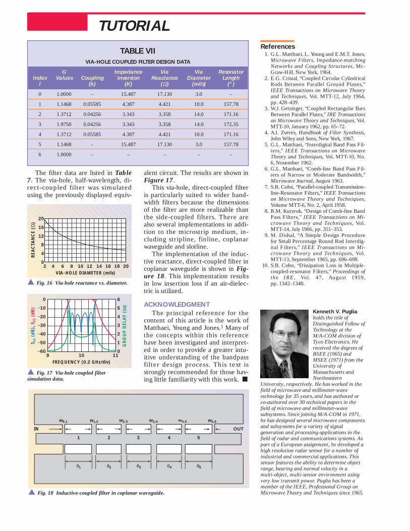
The filter data are listed in Table7. The via-hole, half-wavelength, di-rect-coupled filter was simulatedusing the previously displayed equiv-
alent circuit. The results are shown inFigure 17.
This via-hole, direct-coupled filteris particularly suited to wider band-width filters because the dimensionsof the filter are more realizable thanthe side-coupled filters. There arealso several implementations in addi-tion to the microstrip medium, in-cluding stripline, finline, coplanarwaveguide and slotline.
The implementation of the induc-tive reactance, direct-coupled filter incoplanar waveguide is shown in Fig-ure 18. This implementation resultsin low insertion loss if an air-dielec-tric is utilized.
ACKNOWLEDGMENTThe principal reference for the
content of this article is the work ofMatthaei, Young and Jones.1 Many ofthe concepts within this referencehave been investigated and interpret-ed in order to provide a greater intu-itive understanding of the bandpassfilter design process. This text isstrongly recommended for those hav-ing little familiarity with this work.
References1. G.L. Matthaei, L. Young and E.M.T. Jones,
Microwave Filters, Impedance-matchingNetworks and Coupling Structures, Mc-Graw-Hill, New York, 1964.
2. E.G. Cristal, “Coupled Circular CylindricalRods Between Parallel Ground Planes,”IEEE Transactions on Microwave Theoryand Techniques, Vol. MTT-12, July 1964,pp. 428–439.
3. W.J. Getsinger, “Coupled Rectangular BarsBetween Parallel Plates,” IRE Transactionson Microwave Theory and Techniques, Vol.MTT-10, January 1962, pp. 65–72.
4. A.I. Zverev, Handbook of Filter Synthesis,John Wiley and Sons, New York, 1967.
5. G.L. Matthaei, “Interdigital Band Pass Fil-ters,” IEEE Transactions on MicrowaveTheory and Techniques, Vol. MTT-10, No.6, November 1962.
6. G.L. Matthaei, “Comb-line Band Pass Fil-ters of Narrow or Moderate Bandwidth,”Microwave Journal, August 1963.
7. S.B. Cohn, “Parallel-coupled Transmission-line-Resonator Filters,” IEEE Transactionson Microwave Theory and Techniques,Volume MTT-6, No. 2, April 1958.
8. R.M. Kurzrok, “Design of Comb-line BandPass Filters,” IEEE Transactions on Mi-crowave Theory and Techniques, Vol.MTT-14, July 1966, pp. 351–353.
9. M. Dishal, “A Simple Design Procedurefor Small Percentage Round Rod Interdig-ital Filters,” IEEE Transactions on Mi-crowave Theory and Techniques, Vol.MTT-13, September 1965, pp. 696–698.
10. S.B. Cohn, “Dissipation Loss in Multiple-coupled-resonator Filters,” Proceedings ofthe IRE, Vol. 47, August 1959, pp. 1342–1348.
Kenneth V. Pugliaholds the title ofDistinguished Fellow ofTechnology at the M/A-COM division ofTyco Electronics. Hereceived the degrees ofBSEE (1965) andMSEE (1971) from theUniversity ofMassachusetts andNortheastern
University, respectively. He has worked in thefield of microwave and millimeter-wavetechnology for 35 years, and has authored orco-authored over 30 technical papers in thefield of microwave and millimeter-wavesubsystems. Since joining M/A-COM in 1971,he has designed several microwave componentsand subsystems for a variety of signalgeneration and processing applications in thefield of radar and communications systems. Aspart of a European assignment, he developed ahigh resolution radar sensor for a number ofindustrial and commercial applications. Thissensor features the ability to determine objectrange, bearing and normal velocity in a multi-object, multi-sensor environment usingvery low transmit power. Puglia has been amember of the IEEE, Professional Group onMicrowave Theory and Techniques since 1965.
TUTORIAL
20
16
12
8
4
0201816141210
VIA-HOLE DIAMETER (mils)8642
REA
CTA
NC
E (Ω
)
Fig. 16 Via-hole reactance vs. diameter.
TABLE VIIVIA-HOLE COUPLED FILTER DESIGN DATA
G Impedance Via Via ResonatorIndex Values Coupling Inversion Reactance Diameter Length
i (k) (K) (Ω) (mils) (°)
0 1.0000 – 15.487 17.130 3.0 –
1 1.1468 0.05585 4.387 4.421 10.0 157.78
2 1.3712 0.04256 3.343 3.358 14.0 171.16
3 1.9750 0.04256 3.343 3.358 14.0 172.35
4 1.3712 0.05585 4.387 4.421 10.0 171.16
5 1.1468 – 15.487 17.130 3.0 157.78
6 1.0000 – – – – –
θ5θ4θ3θ2θ1
1
w0,1 w1,2 w2,3 w3,4 w4,5w4w w5,6
OUTIN
2 3 4 5
Fig. 18 Inductive-coupled filter in coplanar waveguide.
0
−10
−20
−30
−40
−50
−60
6
5
4
3
2
1
01110
FREQUENCY (0.2 GHz/div)9
S 11
(dB
), S
21 (
dB)
GR
OU
P D
ELA
Y (n
s)
Fig. 17 Via-hole coupled filter simulation data.

TUTORIALAPPENDIX A
NORMALIZED SELF AND MUTUAL CAPACITANCE OF ROUND RODS BETWEEN PARALLEL GROUND PLANES
Upon completion of specific elements of the design procedure andthe calculation of the normalized self and mutual capacitance per unitlength, rod diameter and center-to-center spacing may be calculated.First, the filter ground plane spacing h must be selected. The selectionof a suitable ground plane spacing is bounded by the out-of-band spu-rious response, passband frequency and insertion loss. Certainly, theground plane dimension should be less than one quarter wavelengthand no smaller than that required to achieve an unloaded Qu consis-tent with the insertion loss requirements. The maximum ground planespacing may be estimated in accordance with
This formula provides the approximate values for ground plane spacinglisted in Table A1:
Cristal2 has given the closed-form expressions for the even and oddmode capacitance per unit length from which the self and mutual ca-pacitance may be calculated from
and
For reasonable accuracy, the parameter m may be limited to 100. Theself and mutual capacitance is calculated using1
Cg(c) = Ce(c)
and
Cm(c) = 0.25[C0(c)–Ce(c)]
The equations have been programmed using Mathcad for a groundplane spacing of 0.275 inches and a rod diameter of 0.128 inches, thatis, Zo = 60 Ω. The data are shown in Figures A1 and A2.
C c
db
db
dbc
b
m cb
e
m
( ) =
+
+ ∑
=
∞
ε
π
ππ1
24
12
12
12
224
4
1ln
–
ln – ln tanh
C c
db
db
dbc
b
m cb
m
m
0
4
4
1
12
4
12
12
12
2 12
( ) =
+ ( )∑
=
∞
ε
π
ππ
ln
–
– ln – – ln tanh
hZ
≤πλ 0 13832
100
TABLE AIAPPROXIMATE VALUES
FOR GROUND PLANE SPACING
Filter Frequency Ground Planef0 (GHz) Spacing h (")
1 3.000
2 1.500
4 0.750
8 0.375
10 0.300
12 0.250
15 0.215
18 0.175
0.80.70.60.50.40.30.20.1
0500450400350
CENTER-TO-CENTER SPACING (mil)300250N
OR
MA
LIZE
D M
UTU
AL
CA
PAC
ITA
NC
E
Fig. A1 Mutual capacitanve of coupled lines for h = 0.275 and d= 0.128".
7.0
6.5
6.0
5.5
5.0
4.5
4.0500450400350
CENTER-TO-CENTER SPACING (mil)300250
NO
RM
ALI
ZED
CA
PAC
ITA
NC
ETO
GR
OU
ND
Fig. A2 Normalized self-capacitance to ground for h = 0.275” and d = 0.128”.
NORMALIZED SELF AND MUTUAL CAPACITANCE OF ROUND RODS BETWEEN PARALLEL GROUND PLANES

TUTORIALAPPENDIX B
ALTERNATE FILTER IMPLEMENTATIONSIn addition to the examples within Part II
of this tutorial, there are several alternative fil-ter implementations that lend themselves tothe general design procedure and should becited. These alternative filter implementationsutilize resonators not fully exploited in recentliterature and for which recent CAD toolshave permitted extensive analysis and under-standing. Two specific types of resonators aresuggested for special applications: cylindricaldielectric resonators and helical resonators.
DIELECTRIC RESONATOR FILTERFigure B1 shows the electrical and me-
chanical schematic of a three-section band-pass filter using cylindrical dielectric res-onators. Resonators of this type are not typicalof conventional lumped or distributed ele-ment structures due to the existence of multi-ple resonant frequencies or modes. This res-onator type permits the design of narrowband,low loss filters due to the high unloaded quali-ty factor (Qu > 10,000) in the principal ordominant resonant mode.
A note of caution is in order with respectto the multiple resonator modes and the envi-ronment necessary to suppress excitation ofthese modes and thereby eliminate loss spikesand spurious responses in the filter transferfunction. There are two techniques suitablefor such a determination. The first techniquerequires experimental characterization of theresonator modes and mode coupling via themethods described in Part I. The second, anduntil recently more difficult analysis, involvesanalytical determination of the modes andmode coupling through the utilization of athree-dimensional electromagnetic simulationtool. Some sophisticated filter designers havemade use of auxiliary modes to design so-called dual-mode or multi-mode filters thatutilize two or more of the resonant modes toobtain very compact, low loss filters with ex-cellent rejection band characteristics. Thegeneral design procedure is not suitable forthis task.
The input, output and inter-resonator cou-pling is accomplished via the magnetic fieldwhich is orthogonal to the circular plane ofthe cylindrical resonator for the dominantTE01δ mode. The equivalent circuit of the di-electric resonator filter represents the electri-cal behavior in the principal mode only. It hasacceptable accuracy if the resonator environ-ment and mounting arrangement has demon-strated elimination of the auxiliary modes.
To obtain the highest unloaded quality fac-tor available from the cylindrical dielectricresonator, a low loss dielectric support struc-ture is required to separate the resonator fromthe electrical ground boundary.
HELICAL RESONATOR FILTERThe helical resonator filter is another filter
type for which the general design procedure isapplicable. Helical resonator filters are partic-ularly useful within the VHF and UHF bandsfor low loss, narrowband applications, andwhere the greater volume of a distributed res-onator filter is prohibitive. The helical res-onator is at least partially distributed due tothe combination of self-inductance and theelectrical length of the coil structure. The he-lical resonator is tuned via the distributed ca-pacitance of the tuning screw at the high elec-tric field point of the resonator. A direct tap atthe low electric field point of the resonator ac-complishes input and output coupling. Theresonator spacing and coupling slot at the highmagnetic field point of the helical structurefacilitates inter-resonator coupling.
Figure B2 shows the mechanical andelectrical schematic of a typical five-sectionhelical resonator filter. Once again, resonatorparameters and coupling coefficients may bedetermined experimentally or analytically bythe use of EM simulation tools. Usually, a lowloss dielectric form that facilitates uniformity,placement and structure supports the helicalresonator.
DIELECTRICRESONATOR
DIELECTRICRESONATOR
COUPLINGSLOT
COUPLINGSLOT
DIELECTRICRESONATOR
OUTPUTCOUPLING
LOOPTUNER
H-FIELD LINES OF TE01δMODE LOW DIELECTRIC SUPPORT
TUNER TUNER
OUTPUTCOUPLING
LOOP
DR3DR2DR1
Fig. B1 Dielectric resonator filter.
SLOT SLOT
TUNER TUNER TUNER TUNER TUNER
SLOTSLOT
Fig. B2 Helical resonator filter.
Copyright © 2022 FDOKUMEN