Further Optimizing EMI with Spread Spectrum
8
Application Report Further Optimizing EMI with Spread Spectrum Alejandro Iraheta ABSTRACT The reduction of electromagnetic interference (EMI) is an inherent issue in all electronic systems as a result of either electromagnetic radiation or electromagnetic conduction. EMI management is one of the most difficult challenges in switch-mode power supply (SMPS) systems due to the switching actions of the power MOSFETs and resulting discontinuous currents. This application report will focus on understanding the noise origins, the effective construction of TI’s Power Modules to help with noise reduction, and how the spread spectrum technique helps reduce EMI emissions. Table of Contents 1 Noise Origin.............................................................................................................................................................................2 1.1 Parasitic Elements............................................................................................................................................................. 2 1.2 High Frequency Noise and Low Frequency Ripple............................................................................................................ 2 2 Effective Construction of a Power Module........................................................................................................................... 3 2.1 Noise Reduction................................................................................................................................................................. 3 2.2 TPSM5601R5H Step-Down Power Module....................................................................................................................... 3 3 Spread Spectrum.................................................................................................................................................................... 4 3.1 Concept.............................................................................................................................................................................. 4 3.2 Tradeoffs............................................................................................................................................................................ 4 3.3 Other EMI Mitigation Techniques....................................................................................................................................... 4 3.4 EMI Results........................................................................................................................................................................ 4 4 Summary................................................................................................................................................................................. 6 5 References.............................................................................................................................................................................. 7 List of Figures Figure 1-1. Buck Converter With Parasitic Elements................................................................................................................... 2 Figure 2-1. Radiated Emissions 24-V Input, 12-V Output, 1.5-A Load........................................................................................ 3 Figure 3-1. EMI Reduction by Spread Spectrum, Frequency Modulation................................................................................... 4 Figure 3-2. Conducted Emissions................................................................................................................................................5 Figure 3-3. Conducted Emissions with Spread Spectrum........................................................................................................... 5 Figure 3-4. Radiated Emissions...................................................................................................................................................5 Figure 3-5. Radiated Emissions with Spread Spectrum.............................................................................................................. 5 Figure 3-6. Output Ripple............................................................................................................................................................ 5 Figure 3-7. Output Ripple with Spread Spectrum........................................................................................................................ 5 Figure 3-8. Efficiency................................................................................................................................................................... 5 Trademarks All trademarks are the property of their respective owners. www.ti.com Table of Contents SLVAF18 – MARCH 2021 Submit Document Feedback Further Optimizing EMI with Spread Spectrum 1 Copyright © 2021 Texas Instruments Incorporated
-
Upload
khangminh22 -
Category
Documents
-
view
0 -
download
0
Transcript of Further Optimizing EMI with Spread Spectrum

Application ReportFurther Optimizing EMI with Spread Spectrum
Alejandro Iraheta
ABSTRACT
The reduction of electromagnetic interference (EMI) is an inherent issue in all electronic systems as a resultof either electromagnetic radiation or electromagnetic conduction. EMI management is one of the most difficultchallenges in switch-mode power supply (SMPS) systems due to the switching actions of the power MOSFETsand resulting discontinuous currents. This application report will focus on understanding the noise origins,the effective construction of TI’s Power Modules to help with noise reduction, and how the spread spectrumtechnique helps reduce EMI emissions.
Table of Contents1 Noise Origin.............................................................................................................................................................................2
1.1 Parasitic Elements............................................................................................................................................................. 21.2 High Frequency Noise and Low Frequency Ripple............................................................................................................2
2 Effective Construction of a Power Module...........................................................................................................................32.1 Noise Reduction.................................................................................................................................................................32.2 TPSM5601R5H Step-Down Power Module....................................................................................................................... 3
3 Spread Spectrum.................................................................................................................................................................... 43.1 Concept..............................................................................................................................................................................43.2 Tradeoffs............................................................................................................................................................................ 43.3 Other EMI Mitigation Techniques....................................................................................................................................... 43.4 EMI Results........................................................................................................................................................................4
4 Summary................................................................................................................................................................................. 65 References.............................................................................................................................................................................. 7
List of FiguresFigure 1-1. Buck Converter With Parasitic Elements...................................................................................................................2Figure 2-1. Radiated Emissions 24-V Input, 12-V Output, 1.5-A Load........................................................................................ 3Figure 3-1. EMI Reduction by Spread Spectrum, Frequency Modulation................................................................................... 4Figure 3-2. Conducted Emissions................................................................................................................................................5Figure 3-3. Conducted Emissions with Spread Spectrum........................................................................................................... 5Figure 3-4. Radiated Emissions...................................................................................................................................................5Figure 3-5. Radiated Emissions with Spread Spectrum.............................................................................................................. 5Figure 3-6. Output Ripple............................................................................................................................................................ 5Figure 3-7. Output Ripple with Spread Spectrum........................................................................................................................ 5Figure 3-8. Efficiency................................................................................................................................................................... 5
TrademarksAll trademarks are the property of their respective owners.
www.ti.com Table of Contents
SLVAF18 – MARCH 2021Submit Document Feedback
Further Optimizing EMI with Spread Spectrum 1
Copyright © 2021 Texas Instruments Incorporated
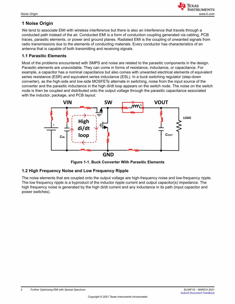
1 Noise OriginWe tend to associate EMI with wireless interference but there is also an interference that travels through aconducted path instead of the air. Conducted EMI is a form of conduction coupling generated via cabling, PCBtraces, parasitic elements, or power and ground planes. Radiated EMI is the coupling of unwanted signals fromradio transmissions due to the elements of conducting materials. Every conductor has characteristics of anantenna that is capable of both transmitting and receiving signals.
1.1 Parasitic ElementsMost of the problems encountered with SMPS and noise are related to the parasitic components in the design.Parasitic elements are unavoidable. They can come in forms of resistance, inductance, or capacitance. Forexample, a capacitor has a nominal capacitance but also comes with unwanted electrical elements of equivalentseries resistance (ESR) and equivalent series inductance (ESL). In a buck switching regulator (step-downconverter), as the high-side and low-side MOSFETs alternate in switching, noise from the input source of theconverter and the parasitic inductance in the high di/dt loop appears on the switch node. The noise on the switchnode is then be coupled and distributed onto the output voltage through the parasitic capacitance associatedwith the inductor, package, and PCB layout.
L
-+
CINCOUT
LOAD
VIN SW
GND
VOUT
High
di/dt
loop
Figure 1-1. Buck Converter With Parasitic Elements
1.2 High Frequency Noise and Low Frequency RippleThe noise elements that are coupled onto the output voltage are high-frequency noise and low-frequency ripple.The low frequency ripple is a byproduct of the inductor ripple current and output capacitor(s) impedance. Thehigh frequency noise is generated by the high di/dt current and any inductance in its path (input capacitor andpower switches).
Noise Origin www.ti.com
2 Further Optimizing EMI with Spread Spectrum SLVAF18 – MARCH 2021Submit Document Feedback
Copyright © 2021 Texas Instruments Incorporated
2 Effective Construction of a Power ModuleA DC/DC power module integrates the controller, power MOSFETs, inductor and other passive components intoa single package. Texas Instrument’s power module family spans isolated and non-isolated architectures aswell as step-up, step-down, and inverting topologies. See TI’s DC/DC power modules broad portfolio for moreinformation.
2.1 Noise ReductionMost power modules integrate a high frequency input capacitor and a shielded inductor. It’s important to notethat the integrated input capacitor greatly reduces the area of the high di/dt loop. A smaller loop area createsa lower ringing on the switch node; lowering the ringing on the switch node will therefore lower the outputnoise. Also, since the switch node is inside the package and has been further reduced, the potential parasiticcapacitance to the other nodes is limited. Although reduced, there are still some parasitic elements present inthe power module.
TI’s Enhanced HotRod™ QFN package technology offers the best in class EMI performance by the removal ofthe wire bonds, which contribute significantly to the parasitic inductance of the power loop (MOSFETs gate loop),and the optimized pin-out of the device to further reduce the parasitic loop inductance. In summary, EnhancedHotRod QFN technology leverages the noise improvements of a flipped chip on lead-frame (FCOL) packageand thermal advantages of the standard QFN package. For a deeper understanding of Enhanced HotRod QFNpackage technology see Enhanced HotRod QFN Package.
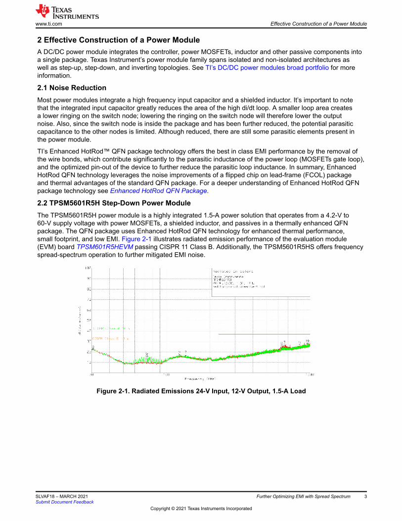
2.2 TPSM5601R5H Step-Down Power ModuleThe TPSM5601R5H power module is a highly integrated 1.5-A power solution that operates from a 4.2-V to60-V supply voltage with power MOSFETs, a shielded inductor, and passives in a thermally enhanced QFNpackage. The QFN package uses Enhanced HotRod QFN technology for enhanced thermal performance,small footprint, and low EMI. Figure 2-1 illustrates radiated emission performance of the evaluation module(EVM) board TPSM601R5HEVM passing CISPR 11 Class B. Additionally, the TPSM5601R5HS offers frequencyspread-spectrum operation to further mitigated EMI noise.
Figure 2-1. Radiated Emissions 24-V Input, 12-V Output, 1.5-A Load
www.ti.com Effective Construction of a Power Module
SLVAF18 – MARCH 2021Submit Document Feedback
Further Optimizing EMI with Spread Spectrum 3
Copyright © 2021 Texas Instruments Incorporated
3 Spread SpectrumSpread Spectrum techniques (or “dithering”) are commonly found in switch-mode power supply systems toreduce the effect of EMI that SMPS generate.
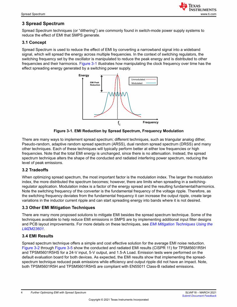
3.1 ConceptSpread Spectrum is used to reduce the effect of EMI by converting a narrowband signal into a widebandsignal, which will spread the energy across multiple frequencies. In the context of switching regulators, theswitching frequency set by the oscillator is manipulated to reduce the peak energy and is distributed to otherfrequencies and their harmonics. Figure 3-1 illustrates how manipulating the clock frequency over time has theeffect spreading energy generated by a switching power supply.
fcFrequency
Energy
Unmodulated
ModulatedEMI Peak
Reduction
Figure 3-1. EMI Reduction by Spread Spectrum, Frequency Modulation
There are many ways to implement spread spectrum; different techniques, such as triangular analog dither,Pseudo-random, adaptive random spread spectrum (ARSS), dual random spread spectrum (DRSS) and manyother techniques. Each of these techniques will typically perform better at either low frequencies or highfrequencies. Note that the total EMI energy is unchanged, since there is no attenuation. Instead, the spreadspectrum technique alters the shape of the conducted and radiated interfering power spectrum, reducing thelevel of peak emissions.
3.2 TradeoffsWhen optimizing spread spectrum, the most important factor is the modulation index. The larger the modulationindex, the more distributed the spectrum becomes; however, there are limits when spreading in a switching-regulator application. Modulation index is a factor of the energy spread and the resulting fundamental/harmonics.Note the switching frequency of the converter is the fundamental frequency of the voltage ripple. Therefore, asthe switching frequency deviates from the fundamental frequency it can increase the output ripple, create largevariations in the inductor current ripple and can start spreading energy into bands where it is not desired.
3.3 Other EMI Mitigation TechniquesThere are many more proposed solutions to mitigate EMI besides the spread spectrum technique. Some of thetechniques available to help reduce EMI emissions in SMPS are by implementing additional input filter designsand PCB layout improvements. For more details on these techniques, see EMI Mitigation Techniques Using theLMZM23601.
3.4 EMI ResultsSpread spectrum technique offers a simple and cost effective solution for the average EMI noise reduction.Figure 3-2 through Figure 3-5 show the conducted and radiated EMI results (CISPR 11) for TPSM5601R5Hand TPSM5601R5HS for a 24-V input, 5-V output, and 1.5-A Load. Emission tests were performed on thedefault evaluation board for both devices. As expected, the EMI results show that implementing the spread-spectrum technique reduced peak emissions while efficiency and output ripple did not have an impact. Note,both TPSM5601R5H and TPSM5601R5HS are compliant with EN55011 Class-B radiated emissions.
Spread Spectrum www.ti.com
4 Further Optimizing EMI with Spread Spectrum SLVAF18 – MARCH 2021Submit Document Feedback
Copyright © 2021 Texas Instruments Incorporated
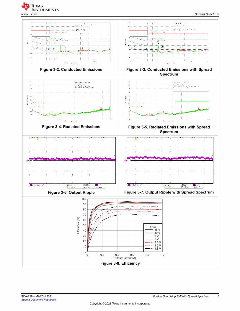
Figure 3-2. Conducted Emissions Figure 3-3. Conducted Emissions with SpreadSpectrum
Figure 3-4. Radiated Emissions Figure 3-5. Radiated Emissions with SpreadSpectrum
Figure 3-6. Output Ripple Figure 3-7. Output Ripple with Spread Spectrum
Output Current (A)
Eff
icie
ncy (
%)
0 0.3 0.6 0.9 1.2 1.50
10
20
30
40
50
60
70
80
90
100
VOUT
15 V12 V9 V5 V3.3 V2.5 V1.8 V
Figure 3-8. Efficiency
www.ti.com Spread Spectrum
SLVAF18 – MARCH 2021Submit Document Feedback
Further Optimizing EMI with Spread Spectrum 5
Copyright © 2021 Texas Instruments Incorporated
4 SummaryEMI can enter a system (or device) through either conduction or radiation, or both. Conducted EMI occursfrom the normal operation of switching circuits. The ON and OFF actions of the power switches generate largediscontinuous currents and pass noise to the output as low frequency ripple and high frequency noise. InEMI-sensitive applications it is important to begin the design with components that have great EMI performance.Texas Instrument’s Enhanced HotRod package technology and power modules are great solutions when itcomes to EMI performance.
To further optimize EMI performance, implementing spread-spectrum architecture offers a simple and costeffective solution for the average EMI noise reduction by reducing harmonic peaks and spreading the noiseenergy. As a result, the measured radiated and conducted peak emissions are reduced, however, the total-noiseenergy is unchanged and other bands can be negatively affected depending on the application.
Summary www.ti.com
6 Further Optimizing EMI with Spread Spectrum SLVAF18 – MARCH 2021Submit Document Feedback
Copyright © 2021 Texas Instruments Incorporated

5 References• Texas Instruments, Enhanced HotRod QFN Package: Achieving Low EMI Performance in Industry's Smallest
4-A Converter application report.• Texas Instruments, EMI Mitigation Techniques Using the LMZM23601 application report.• Texas Instruments, EMI Reduction Technique, Dual Random Spread Spectrum application report.• Texas Instruments, Low Conducted EMI Power Solution for Automotive Digital Cockpit With LMR14050 and
TPS65263 application report.• Texas Instruments, Output Noise Filtering for DC/DC Power Modules application report.• Texas Instruments, Passing CISPR-25 Radiated and Conduction Emissions Using the TPS65033x-Q1
application report.• Texas Instruments, Reduce buck-converter EMI and voltage stress by minimizing inductive parasitics Analog
Applications Journal.• Texas Instruments, Simple Succes with Conducted EMI and Radiated EMI for LMR160X0 application report.• Texas Instruments, Understanding Noise-Spreading Techniques and their Effects in Switch-Mode Power
Applications
www.ti.com References
SLVAF18 – MARCH 2021Submit Document Feedback
Further Optimizing EMI with Spread Spectrum 7
Copyright © 2021 Texas Instruments Incorporated

IMPORTANT NOTICE AND DISCLAIMERTI PROVIDES TECHNICAL AND RELIABILITY DATA (INCLUDING DATA SHEETS), DESIGN RESOURCES (INCLUDING REFERENCE DESIGNS), APPLICATION OR OTHER DESIGN ADVICE, WEB TOOLS, SAFETY INFORMATION, AND OTHER RESOURCES “AS IS” AND WITH ALL FAULTS, AND DISCLAIMS ALL WARRANTIES, EXPRESS AND IMPLIED, INCLUDING WITHOUT LIMITATION ANY IMPLIED WARRANTIES OF MERCHANTABILITY, FITNESS FOR A PARTICULAR PURPOSE OR NON-INFRINGEMENT OF THIRD PARTY INTELLECTUAL PROPERTY RIGHTS.These resources are intended for skilled developers designing with TI products. You are solely responsible for (1) selecting the appropriate TI products for your application, (2) designing, validating and testing your application, and (3) ensuring your application meets applicable standards, and any other safety, security, regulatory or other requirements.These resources are subject to change without notice. TI grants you permission to use these resources only for development of an application that uses the TI products described in the resource. Other reproduction and display of these resources is prohibited. No license is granted to any other TI intellectual property right or to any third party intellectual property right. TI disclaims responsibility for, and you will fully indemnify TI and its representatives against, any claims, damages, costs, losses, and liabilities arising out of your use of these resources.TI’s products are provided subject to TI’s Terms of Sale or other applicable terms available either on ti.com or provided in conjunction with such TI products. TI’s provision of these resources does not expand or otherwise alter TI’s applicable warranties or warranty disclaimers for TI products.TI objects to and rejects any additional or different terms you may have proposed. IMPORTANT NOTICE
Mailing Address: Texas Instruments, Post Office Box 655303, Dallas, Texas 75265Copyright © 2022, Texas Instruments Incorporated