
Power Efficiency and EMI Attenuation Optimization in Filter ...
9
HAL Id: hal-01887159 https://hal.archives-ouvertes.fr/hal-01887159 Submitted on 15 Oct 2018 HAL is a multi-disciplinary open access archive for the deposit and dissemination of sci- entific research documents, whether they are pub- lished or not. The documents may come from teaching and research institutions in France or abroad, or from public or private research centers. L’archive ouverte pluridisciplinaire HAL, est destinée au dépôt et à la diffusion de documents scientifiques de niveau recherche, publiés ou non, émanant des établissements d’enseignement et de recherche français ou étrangers, des laboratoires publics ou privés. Power Effciency and EMI Attenuation Optimization in Filter Design Moises Ferber, Roberto Mrad, Florent Morel, Gaël Pillonnet, Christian Vollaire, Angelo Nagari To cite this version: Moises Ferber, Roberto Mrad, Florent Morel, Gaël Pillonnet, Christian Vollaire, et al.. Power Ef- ficiency and EMI Attenuation Optimization in Filter Design. IEEE Transactions on Electromag- netic Compatibility, Institute of Electrical and Electronics Engineers, 2018, 60 (6), pp.1811 - 1818. 10.1109/TEMC.2017.2765921. hal-01887159
-
Upload
khangminh22 -
Category
Documents
-
view
1 -
download
0
Transcript of Power Efficiency and EMI Attenuation Optimization in Filter ...
HAL Id: hal-01887159https://hal.archives-ouvertes.fr/hal-01887159
Submitted on 15 Oct 2018
HAL is a multi-disciplinary open accessarchive for the deposit and dissemination of sci-entific research documents, whether they are pub-lished or not. The documents may come fromteaching and research institutions in France orabroad, or from public or private research centers.
L’archive ouverte pluridisciplinaire HAL, estdestinée au dépôt et à la diffusion de documentsscientifiques de niveau recherche, publiés ou non,émanant des établissements d’enseignement et derecherche français ou étrangers, des laboratoirespublics ou privés.
Power Efficiency and EMI Attenuation Optimization inFilter Design
Moises Ferber, Roberto Mrad, Florent Morel, Gaël Pillonnet, ChristianVollaire, Angelo Nagari
To cite this version:Moises Ferber, Roberto Mrad, Florent Morel, Gaël Pillonnet, Christian Vollaire, et al.. Power Ef-ficiency and EMI Attenuation Optimization in Filter Design. IEEE Transactions on Electromag-netic Compatibility, Institute of Electrical and Electronics Engineers, 2018, 60 (6), pp.1811 - 1818.10.1109/TEMC.2017.2765921. hal-01887159

Power Efficiency and EMI AttenuationOptimization in Filter Design
Moises Ferber, Roberto Mrad, Florent Morel, Senior Member, IEEE, Gael Pillonnet, Member, IEEE,Christian Vollaire, Member, IEEE and Angelo Nagari, Senior Member, IEEE
Abstract—This paper presents a discrete conducted electro-magnetic interference filter optimization procedure, based ona Genetic Algorithms. A macro-modeling technique taking intoaccount the load impedance, the source emissions and the filterparasitic components, including the filter layout, is used toobtain an accurate solution for the optimization process. Thelatter searches among supplier passive component databases andprovides, for a given filter topology, an optimal set of componentsavailable on the market. This approach has been applied to adifferential Class-D audio amplifier for validation. By consideringthe EMI, the additional power losses introduced by the filterand the audio gain, two different optimization formulations havebeen tested. The first corresponds to maximizing the powerefficiency of the system while respecting a determined level ofelectromagnetic emissions. The second corresponds to minimizingthe EMI without exceeding a determined level of power loss. Theoptimized filters are built and measurements are carried out. Theresults show a remarkable power efficiency improvement and asignificant EM emission reduction when compared to a referencefilter.
Index Terms—Conducted immunity and emissions, Filtering,Passive component modeling and measurement techniques, Powerelectronics, Printed circuit board EMC.
I. INTRODUCTION
Nowadays, electronic devices demand high power due tothe diversity of applications in the same device. Switchingpower converters and power management circuits are thereforewidely used. Generally, such circuits have high electromag-netic (EM) emissions, because they deal with switching signalsand they provide higher power, compared to their surroundingelectronics. To avoid any system dysfunction, electromagneticinterference (EMI) filters are used in most cases. A filter’sperformance is measured by its high frequency insertion loss.Therefore, stray elements have a direct impact on the filter’seffectiveness [1]. Moreover, EMI filters are in the electricalpower path and if they are not adequately designed, they canlead to high power losses due to parasitic resistances. Thus,they can reduce the overall power efficiency.
To confirm this issue, power measurements on a low powerClass-D amplifier for a hands-free mobile phone applicationhave been made, with zero and low audio signal level (-20 dBfull scale). At the supply pin, we recorded an average of10 mW and 50 mW of power consumption when the amplifieris used without and with an EMI filter, respectively. Therefore,due to the EMI filter, the system consumes 5 times more atlow output power. In [2], it has been shown that in a realaudio signal (i.e. Jazz song), there are more amplitude levelslower than -20 dB full scale than the higher amplitudes for
a 10 s recording. Thus, it can be deduced that a Class-Damplifier runs most of the time at low signal levels. As aresult, the additional power losses due to the EMI filter is acrucial parameter in filter design for battery-powered, audioapplications.
Some electromagnetic compatibility experts rely on expe-rience to design EMI filters. Other designers refer to theclassical filter design methodology, which consists in de-termining the required attenuation of conducted emissionsrelative to a given EMI standard or system specification, andthen computing the values of inductances and capacitancesanalytically for a given topology [3]–[9]. These proceduresmay lead to sub-optimal solutions for EMC, volume, area andspecially power efficiency. Thus, the filter design formulatedas an optimization problem can be advantageous. Even thoughone can find many papers about EMI filter design, to thebest knowledge of the authors, no work has investigated yetthe problem of maximizing the power efficiency of an EMIfilter, while keeping a determined level of EMI attenuationor maximizing EMI attenuation, while keeping a determinedlevel of power efficiency.
A continuous optimization procedure has already been ap-plied to EMI filter design for power electronics [10], [11],for aerospace applications [12], [13] and for signal process-ing [14]. However, this type of optimization can be improved.Passive filters are constituted of standard components availableon the market, such as surface mounted technology (SMT)components. These have discrete nominal values. Componentnominal values given by a continuous optimization are mostof the time unavailable from suppliers. Additionally, SMTcomponent suppliers provide component libraries that take intoaccount high frequency behavior. Therefore, optimizing a filteraccording to the available components on the market is muchmore realistic.
The number of available components on the market, con-sidering all suppliers, is very high. For instance, a filter of 5components and 100 items per component, which is a fairlysmall problem, corresponds to a discrete design space of size(102)5 = 1010. Considering that each function evaluationtakes about 1 s, the time required for an exhaustive searchwould be more than three hundred years, thus, impractical.Discrete optimization methods are able to explore a very smallsubset of the design space and find the global optimal or adesign which is near to the global optimal.
Previous work in filter optimization such as [15]–[19],neglect or give less importance to the parasitic effects of com-ponents and printed circuit board (PCB) tracks. Nevertheless,
this part is essential in high frequency EMI modeling. In [20],the equivalent series resistance, capacitance and inductanceof passive components are modeled with lumped circuit el-ements as an attempt to increase accuracy in EMC analysisand optimization. However, there is no simple expressionthat links these parasitic effects to the component nominalvalue. Therefore, using the component models provided bythe supplier is the most adequate choice.
In [21], the authors propose an automated filter designbased on discrete optimization by Genetic Algorithms (GAs).The optimization runs on a sub-system level macro-modelingtechnique in the frequency domain which relies on impedancematrix manipulation. The approach is presented in [22], [23].It allows the source emissions and the load impedance tobe included for a fast and accurate electromagnetic emissioncomputation. The filter, having a fixed topology [24], isimplemented in Advanced System Design (ADS) software.Therefore, most of the filter imperfections such as the PCBlayout and PCB stray components are taken into account.The filter components are replaced by their models providedby the suppliers in a library of models referring to theirproducts. The GA searches among these components andgenerates an impedance matrix from the ADS filter model.Finally, based on the criterion calculated using the macro-model, the optimization process extracts a set of componentscorresponding to the optimal solution. Note that the componentreferences are given and they can be found on the market.
The present paper extends [21], by giving more detailsabout the optimization and testing two different problemformulations. The first formulation aims to maximize thefilter power efficiency while respecting the EM emissionlimit. The second formulation aims to reduce the system EMemissions without decreasing the system power efficiency.Both formulations are solved numerically and validated withexperimental measurements. Finally, a comparison betweenthe two formulations is made to highlight the existing trade-offbetween power efficiency and EMC performance.
The remainder of this paper is organized as follows: inSection II, the problem formulation is presented. Then, inSection III, the modeling method, the power computationexpressions and the optimization methodology are depicted. InSection IV, the application on a Class-D amplification systemis presented. Section V presents the experimental results.Finally, in Section VI, a conclusion is presented.
II. PROBLEM FORMULATION
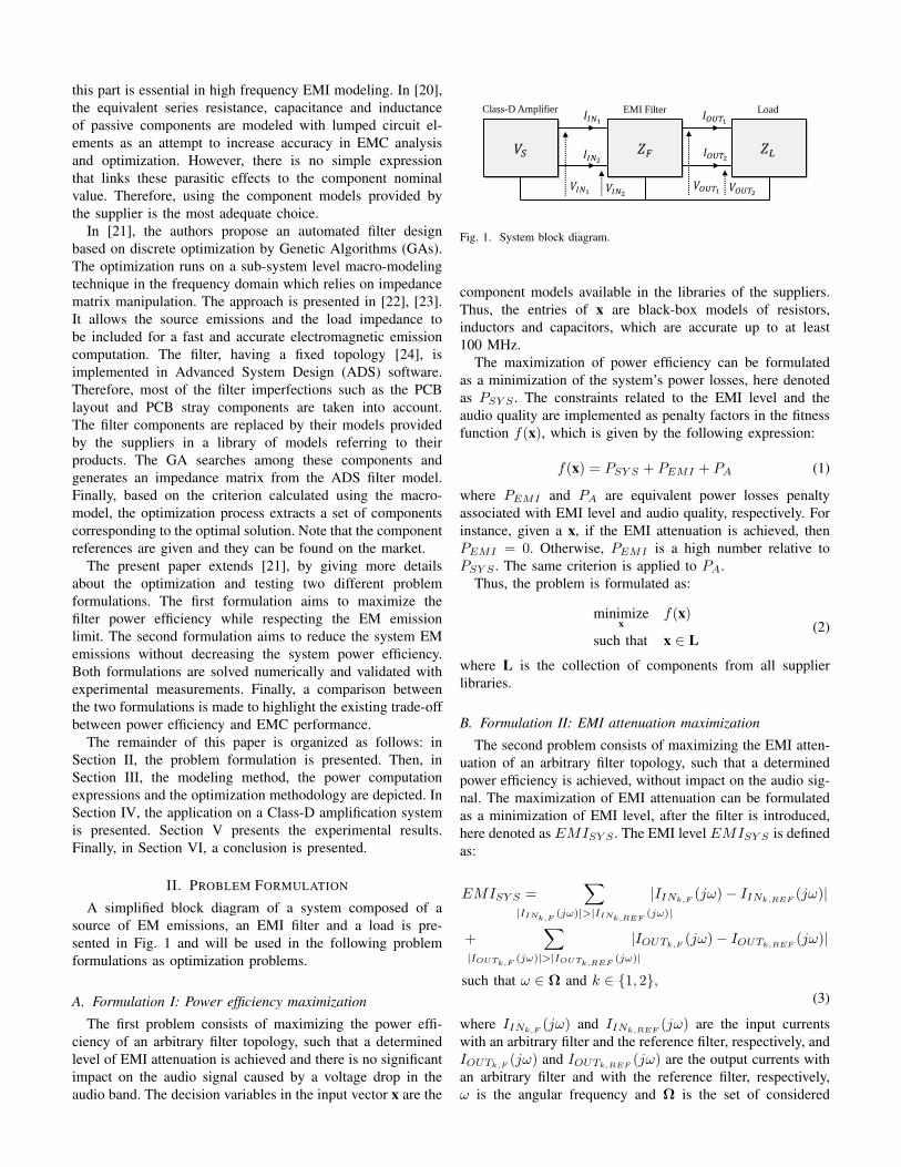
A simplified block diagram of a system composed of asource of EM emissions, an EMI filter and a load is pre-sented in Fig. 1 and will be used in the following problemformulations as optimization problems.
A. Formulation I: Power efficiency maximization
The first problem consists of maximizing the power effi-ciency of an arbitrary filter topology, such that a determinedlevel of EMI attenuation is achieved and there is no significantimpact on the audio signal caused by a voltage drop in theaudio band. The decision variables in the input vector x are the
𝑍𝐹 𝑍𝐿
EMI Filter LoadClass-D Amplifier
𝑉𝑆
𝐼𝐼𝑁1
𝑉𝐼𝑁1
𝐼𝐼𝑁2
𝐼𝑂𝑈𝑇1
𝐼𝑂𝑈𝑇2
𝑉𝐼𝑁2𝑉𝑂𝑈𝑇1 𝑉𝑂𝑈𝑇2
Fig. 1. System block diagram.
component models available in the libraries of the suppliers.Thus, the entries of x are black-box models of resistors,inductors and capacitors, which are accurate up to at least100 MHz.
The maximization of power efficiency can be formulatedas a minimization of the system’s power losses, here denotedas PSY S . The constraints related to the EMI level and theaudio quality are implemented as penalty factors in the fitnessfunction f(x), which is given by the following expression:
f(x) = PSY S + PEMI + PA (1)
where PEMI and PA are equivalent power losses penaltyassociated with EMI level and audio quality, respectively. Forinstance, given a x, if the EMI attenuation is achieved, thenPEMI = 0. Otherwise, PEMI is a high number relative toPSY S . The same criterion is applied to PA.
Thus, the problem is formulated as:
minimizex
f(x)
such that x ∈ L(2)
where L is the collection of components from all supplierlibraries.
B. Formulation II: EMI attenuation maximization
The second problem consists of maximizing the EMI atten-uation of an arbitrary filter topology, such that a determinedpower efficiency is achieved, without impact on the audio sig-nal. The maximization of EMI attenuation can be formulatedas a minimization of EMI level, after the filter is introduced,here denoted as EMISY S . The EMI level EMISY S is definedas:
EMISY S =∑
|IINk,F(jω)|>|IINk,REF
(jω)|
|IINk,F(jω)− IINk,REF
(jω)|
+∑
|IOUTk,F(jω)|>|IOUTk,REF
(jω)|
|IOUTk,F(jω)− IOUTk,REF
(jω)|
such that ω ∈ Ω and k ∈ 1, 2,(3)
where IINk,F(jω) and IINk,REF
(jω) are the input currentswith an arbitrary filter and the reference filter, respectively, andIOUTk,F
(jω) and IOUTk,REF(jω) are the output currents with
an arbitrary filter and with the reference filter, respectively,ω is the angular frequency and Ω is the set of considered

frequencies. In other words, EMISY S is the sum of thedifferences between the module of the current spectrum peaksof a given filter and those of the reference filter when thepeaks are lower then the ones of the reference filter.
If no reference filter exists, one may use IINk,DESand
IOUTk,DESinstead of IINk,REF
and IOUTk,REF, respectively,
where the subscript DES refers to a maximum desired valuefor the current flowing in the power path.
The constraints related to the power efficiency level andthe audio quality are also implemented as penalty factors inthe fitness function f(x), which is given by the followingexpression:
f(x) = EMISY S + EMIη + EMIA (4)
where EMIη and EMIA are equivalent EMI penalties associ-ated with power efficiency level and audio quality, respectively.For instance, given a x, if a determined power efficiencyis achieved, then EMIη = 0. Otherwise, EMIη is a highnumber relative to EMISY S . The same criterion is appliedto EMIA. The penalties are applied if any current peak ofthe given filter spectrum exceeds the one obtained with thereference filter.
Here, the problem formulation is identical to (2) with f(x)given by (4).
III. METHODOLOGY
The methodology developed in this paper is presented inthree subsections as follows.
A. Modeling approach
A frequency-domain modeling approach presented in [22]was used. This method was chosen because it is a subsystemlevel macro-modeling technique. It can be easily applied onsingle phase systems such as DC-DC converters [25], differen-tial systems such as the integrated Class-D amplifiers [23] oreven N-phase systems. This approach is particularly interestingfor studying the filter in the final application, according to aspecific EMI source and load with a good accuracy at highfrequencies.
An accuracy limitation of this modeling approach is relatedto not taking into account the electric and magnetic couplingbetween components and between component and PCB tracks,which can be very important [26], [27]. However, this modelhas a short simulation time compared to the traditional tran-sient simulations, which is a great advantage when integratedin an optimization loop in EMI filter design.
The considered frequency modeling approach consists indecomposing the system into functional blocks, as shown inFig. 1. Three blocks can be seen in this figure: the Class-D amplifier, the filter and the load. The Class-D amplifier ismodeled by electric sources and an impedance matrix thatcorresponds to the Class-D amplifier output impedance. Theload is modeled by an impedance matrix if it is a passiveload or by electric sources and an impedance matrix if it is anactive load. The sources and impedance matrices of the Class-D amplifier and load can be measured or simulated. Finally, the
filter is modeled by an impedance matrix that can be obtainedby a dedicated analytical model or an implemented model ina simulation software. The model of each filter component, ifnot given by the supplier, can be obtained by, an impedancemeasurement, a scattering parameter measurement, or by theirequivalent analytical or fitting models. More details can befound in [22].
Many possibilities can be used to compute the filterimpedance matrix. The filter high frequency behavior dependson the filter parasitic stray elements. In this work, the ADSsoftware [28] is used to model the filter. The model includesthe filter layout design and all the PCB physical characteristics.Thus, the stray elements related to the filter layout such astrack impedance are taken into account. In this model, thecomponents are black-box models provided by the suppliers.Hence, the passive component stray elements related to thetechnology and packaging of each component are taken intoaccount. Finally, the ADS generates an impedance matrixincluding most of the filter stray elements and non-idealimpedance behavior for better accuracy at high frequencies.
B. Power computation
Using the model presented earlier, it is possible to computevoltages and currents at any system node. Hence, the powerlosses of a system (PSY S), composed of a Class-D amplifier,filter and load losses are computed as follows:
PSY S = PPS + PFL − PA︸ ︷︷ ︸filter and load losses
(5)
where PPS represents the losses in the power stage, PFLrepresent the power delivered to the filter and the load, PAis the power of the audio signal. They can be obtained byequations (6), (7) and (8), respectively.
PPS = RDSon(I2IN1+ I2IN2
) (6)
where RDSon is the power switch-on resistor, IIN1 and IIN2
are the RMS input currents of the filter, which are the sameas the power stage output currents.
PFL =
n∑k=1
RealVIN1(fk) · I∗IN1
(fk)+
RealVIN2(fk) · I∗IN2(fk)
(7)
where VIN1and VIN2
are the filter input voltages and k is theindex of the frequency vector of size n. Note that PFL alsoincludes the power in the audio band. Therefore, PA must becomputed and deduced from the total power loss PSY S in (5).
PA = Real[VOUT1(fA)− VOUT2
(fA)] · I∗OUT1(fA) (8)
where VOUT1(fA) and VOUT2(fA) are the filter output volt-ages and IOUT1(fA) is the filter output current, all at the audiofrequency fA. Here, the considered audio signal is a pure sinewave.
InitializeYPopulation
EvaluatePopulation
ReturnYBestIndividual
GeneticYOperators(Mutation,YCrossover,YSelection)
ConversionYCriteriaYmet?
Yes
No
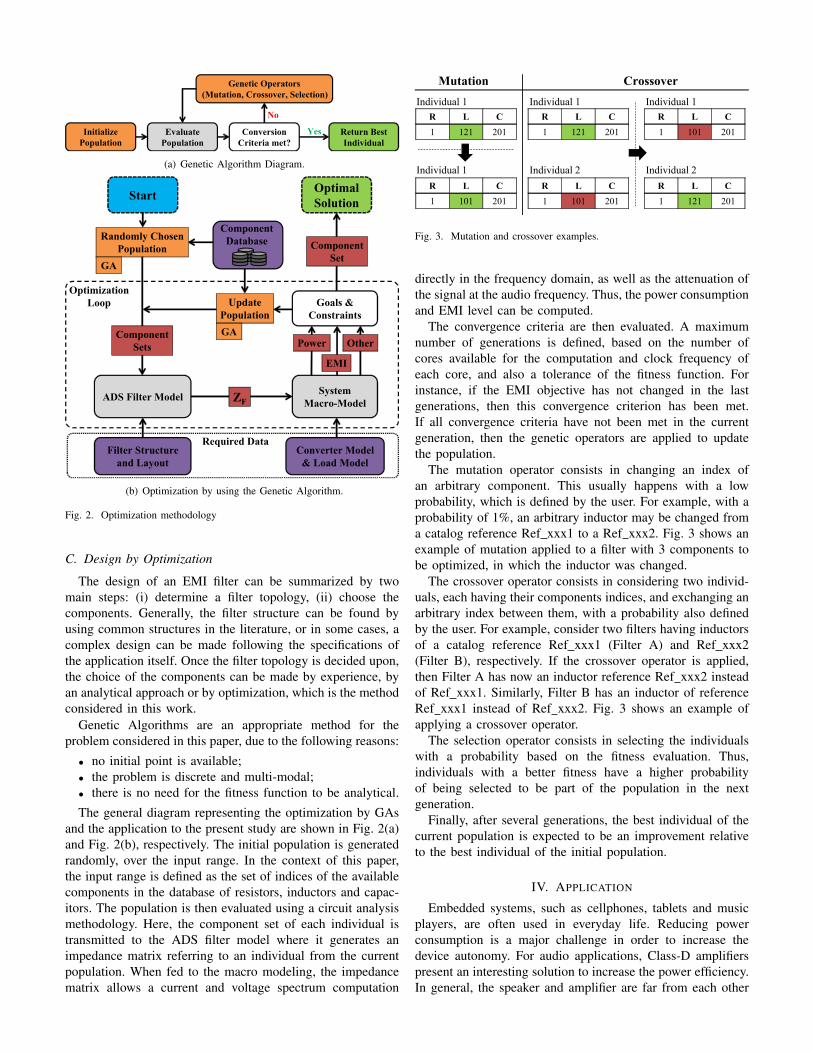
(a) Genetic Algorithm Diagram.
GoalsUqConstraints
EMI
Power Other
RandomlyUChosenUPopulation
SystemUMacro-ModelZF
UpdatePopulation
ComponentDatabase
ADSUFilterUModel
OptimalSolution
GA
GA
Start
FilterUStructureUandULayout
ConverterUModelqULoadUModel
RequiredUData
OptimizationLoop
ComponentSets
ComponentSet
(b) Optimization by using the Genetic Algorithm.
Fig. 2. Optimization methodology
C. Design by Optimization
The design of an EMI filter can be summarized by twomain steps: (i) determine a filter topology, (ii) choose thecomponents. Generally, the filter structure can be found byusing common structures in the literature, or in some cases, acomplex design can be made following the specifications ofthe application itself. Once the filter topology is decided upon,the choice of the components can be made by experience, byan analytical approach or by optimization, which is the methodconsidered in this work.
Genetic Algorithms are an appropriate method for theproblem considered in this paper, due to the following reasons:• no initial point is available;• the problem is discrete and multi-modal;• there is no need for the fitness function to be analytical.The general diagram representing the optimization by GAs
and the application to the present study are shown in Fig. 2(a)and Fig. 2(b), respectively. The initial population is generatedrandomly, over the input range. In the context of this paper,the input range is defined as the set of indices of the availablecomponents in the database of resistors, inductors and capac-itors. The population is then evaluated using a circuit analysismethodology. Here, the component set of each individual istransmitted to the ADS filter model where it generates animpedance matrix referring to an individual from the currentpopulation. When fed to the macro modeling, the impedancematrix allows a current and voltage spectrum computation
R L C
1 121 201
R L C
1 101 201
Mutation Crossover
Individual 1
Individual 2
R L C
1 121 201
R L C
1 101 201
Individual 1
Individual 1
Individual 1
Individual 2
R L C
1 101 201
R L C
1 121 201
Fig. 3. Mutation and crossover examples.
directly in the frequency domain, as well as the attenuation ofthe signal at the audio frequency. Thus, the power consumptionand EMI level can be computed.
The convergence criteria are then evaluated. A maximumnumber of generations is defined, based on the number ofcores available for the computation and clock frequency ofeach core, and also a tolerance of the fitness function. Forinstance, if the EMI objective has not changed in the lastgenerations, then this convergence criterion has been met.If all convergence criteria have not been met in the currentgeneration, then the genetic operators are applied to updatethe population.
The mutation operator consists in changing an index ofan arbitrary component. This usually happens with a lowprobability, which is defined by the user. For example, with aprobability of 1%, an arbitrary inductor may be changed froma catalog reference Ref xxx1 to a Ref xxx2. Fig. 3 shows anexample of mutation applied to a filter with 3 components tobe optimized, in which the inductor was changed.
The crossover operator consists in considering two individ-uals, each having their components indices, and exchanging anarbitrary index between them, with a probability also definedby the user. For example, consider two filters having inductorsof a catalog reference Ref xxx1 (Filter A) and Ref xxx2(Filter B), respectively. If the crossover operator is applied,then Filter A has now an inductor reference Ref xxx2 insteadof Ref xxx1. Similarly, Filter B has an inductor of referenceRef xxx1 instead of Ref xxx2. Fig. 3 shows an example ofapplying a crossover operator.
The selection operator consists in selecting the individualswith a probability based on the fitness evaluation. Thus,individuals with a better fitness have a higher probabilityof being selected to be part of the population in the nextgeneration.
Finally, after several generations, the best individual of thecurrent population is expected to be an improvement relativeto the best individual of the initial population.
IV. APPLICATION
Embedded systems, such as cellphones, tablets and musicplayers, are often used in everyday life. Reducing powerconsumption is a major challenge in order to increase thedevice autonomy. For audio applications, Class-D amplifierspresent an interesting solution to increase the power efficiency.In general, the speaker and amplifier are far from each other

VIn
VRampVCM VOut
VBat
VBat
VPWM-p
VPWM-n
+-
-+
+
-
+-
Fig. 4. Class-D amplifier differential architecture [29] without EMI filter.
due to their placement on the PCB. Therefore, as the Class-D amplifier is a switching circuit, an EMI filter is used tomitigate the flow of high frequency currents through the longPCB tracks that connect the amplifier to the loudspeaker. Thesecurrents may be the cause of radiated emission problems.Thus, this application is a good example for the validationof the proposed method.
In the next subsection we start by giving an overview ofClass-D amplifiers. The filter architecture, the SMT compo-nent libraries and the load in use are then presented. Finally,the additional power losses introduced by the EMI filter arethen exposed and their calculation is explained.
A. Class-D amplifier
A Class-D amplifier is a switching device composed of aswitching power stage controlled by Pulse Width Modula-tion (PWM) [29]. Generally, in integrated solutions such ascell phones, differential architectures are used due to higherpower delivery characteristics. The modulation is obtained bycomparing the audio signal to a ramp at around a 400 kHz.Two alternating opposite width PWM signals are obtained(see Fig. 4), that control two switching cells which form thepower stage. The latter feeds the speaker load by the amplifiedswitched audio signal. Note that this type of amplifier, alsocalled filterless Class-D amplifier, does not need a filter toreconstitute the audio signal due to the inductive nature of themicro-speakers [30] and because the switching harmonics areoutside the audio frequency band. A filter is only needed forEMC reasons.
In this work, a test chip of a classical PWM differentialClass-D amplifier is used. The amplifier output voltages havebeen measured for the same operating points in three differentload conditions. The first is the operation with an open circuit,the second is the operation with a speaker load and the thirdis the operation with an EMI filter and a speaker load. Onlytwo cases are shown in Fig. 5 for a clearer presentation of theresults. The spectra are identical over the considered frequencyband. Thus, it can be deduced that the amplifier voltage isindependent of the load and the amplifier output impedance isnegligible over the frequency range.
Fig. 5. Amplifier output voltage for two different load conditions.
Several simulations and measurements of the output volt-ages of the Class-D amplifier aforementioned were carriedout. The worst-case scenario of audio signal considering EMIlevel is when the amplifier is operating with low input audio.Therefore, this scenario was used in the optimization. TheClass-D amplifier output voltages considered are shown inFig. 5.
B. Load
The load has been chosen as a dummy load that emulatesthe speaker. It is composed of an 8 Ω resistor and two15 µH inductors mounted on a PCB. As a passive load, it canbe modeled as an impedance matrix. Therefore, it has beenmeasured using an impedance analyzer as explained in [22].
C. EMI filter and passive components
In [24], an EMI filter topology for Class-D amplifiers ispresented, which is also shown in Fig. 6. It has been chosenas a reference filter to validate our optimization approach.This common and differential mode filter has nine componentswhich include two inductors, two resistors and five capacitors.To ensure the symmetrical nature of the filter, thus, avoidingany differential to common mode conversion, and vice versa,some components must be identical. Hence, the problemconsists of choosing the components L1, R1, C1, C3 andC4, the five parameters to be optimized. The parameters R2,L2, C2 and C5 are automatically chosen by symmetry. Thistopology has been implemented in the ADS [31] software, forthe optimization routine. The PCB tracks have been modeledas microstrip lines. The PCB characteristics have also beentaken into account.
The libraries of SMT components have been chosen inthe following manner: the inductors can be selected fromTDK [32] and Murata [33] suppliers whereas the capacitorsonly from Murata. The resistors are chosen from a set ofdiscrete values, since their impact on the results are muchsmaller than the other components. Thus, a database has been

L1
L2 C3
C2 C1R1 R2
C4 C5
Vin2Vin1
Vout2Vout1
Iin1
Iin2
Iout1
Iout2
Fig. 6. Class-D EMI filter in use.
𝑳𝟏
𝑳𝟐
𝑪𝟑
𝑪𝟒
𝑪𝟓
𝑹𝟏
𝑹𝟐
𝑪𝟏
𝑪𝟐
Fig. 7. Filter layout.
created in MATLAB referring to these three libraries to beincluded in the optimization routine. Note that as the footprintof each filter component must be chosen for the layout, thecapacitors have been defined as a 1005 (metric) SMT packageand the inductors as a 7045 (metric) SMT package. In total,there are 718 capacitors, 8 inductors and 93 resistors in thedatabase, with ranges of 0.1 pF to 10 µF, 1.5 µH to 22 µHand 1.0 Ω to 10 kΩ, respectively.
V. EXPERIMENTAL RESULTS
The optimization routine based on Genetic Algorithms wasexecuted in the MATLAB-ADS framework. The computerused is an Intel Quad Core i7 2.50 GHz with 16 GB of RAMmemory. The entire optimization process required 3 hours,5 minutes and 7 seconds for the power efficiency case and3 hours, 5 minutes and 26 seconds for the EMI attenuationcase. There is no reason to explain the differences betweenthese optimization processes except variable computer back-ground processes. The reference filter as well as the optimizedfilters according to power efficiency and EMI attenuation arepresented in Table I.
Prototypes for all filters shown in Table I have been builtand used in the measurement validation. The filter layout is thesame for all the filters and is shown in Fig. 7. The measurementbench with the prototypes (see Fig. 8) has been placed in ananechoic chamber to reduce the ambient EM noise. The inputcurrents, output voltages and output currents are measuredwith a current probe [34] and voltage probe connected to ahigh resolution oscilloscope [35]. The measurement probeshave an impact on the spectra results, since they add parasiticstray components when connected to the circuit. Therefore,the parasitic effect of the probes were taken into account whencomparing simulation and measurement results.
In Fig. 9, it is shown a comparison between measured andsimulated input currents for the reference filter, in order to
Fig. 8. Hardware for experimental results.
Fig. 9. Filter input current.
validate the accuracy of the modeling approach. The inputcurrent is chosen, as it has a higher spectrum level than themeasurement noise floor. Thus, it is possible to make a goodcomparison over the entire frequency range. In Fig. 9, it isshown that the measured and the simulated input currentsare in good agreement well up to 100 MHz, which is themeasurement setup accuracy and model validity limit.
The output currents of the optimized filters are very low,in fact lower than the measurement noise floor. Therefore,the measured output voltages are shown for comparison. InFig. 10, it is shown the envelopes of the output voltages, whichare the voltages on the load, in the following cases: (1) nofilter is used, (2) the reference filter is used and (3) the powerefficiency optimized filter is used (formulation I) and finally,(4) the EMI attenuation optimized filter (formulation II) isused.
It can be seen that no significant variations occur in the au-dio signal level at 10 kHz which is due to the audio constraintin the objective functions. In addition, the spectrum peaks arehigher when there is no EMI filter. A considerable emissionreduction can be observed when introducing any filter. Inparticular, the optimized filters offer a significant reductionin the spectrum compared to the reference filter, speciallyat around 400 kHz. The output spectrum has approximately20 dB of additional reduction compared to the reference filter.Between 5 MHz and 50 MHz, the voltage level is lower thanthe measurement noise floor, and so no comparison is possible.Beyond 50 MHz, the reference filter has a better EMI behavior.
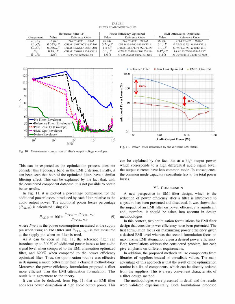
TABLE IFILTER COMPONENT VALUES
Reference Filter [24] Power Efficiency Optimized EMI Attenuation OptimizedComponent Value Reference Code Value Reference Code Value Reference CodeL1, L2 15µH CLF7045T − 150M 22µH CLF7045T − 220M 22µH CLF7045T − 220M
C1, C2 0.033µF GRM155R71C333KA01 0.74µF GRM155R60J474KE19 0.1µF GRM155R61H104KE19
C4, C5 0.068µF GRM155R61A683KA01 1.2 pF GRM1535C1H1R2CDD5 0.1µF GRM155R61H104KE19
C3 0.15µF GRM155R61A154KE19 0.1µF GRM155R61H104KE19 0.47µF LLL153C70G474ME17
R1, R2 22 Ω CPF0402B22RE1 1.6 Ω MC0.0625W04021%1R60 1.3 Ω MC0.0625W04021%1R30
104
105
106
107
108
30
40
50
60
70
80
90
100
110
120
130
FCHz)
dBµ
V
NofFilterfCEnvelope)ReferencefFilterfCEnveloppe)PowfLossfOptfCEnvelope)EMCfOptfCEnvelope)NoisefCEnvelope)
Fig. 10. Measurement comparison of filter’s output voltage envelopes.
This can be expected as the optimization process does notconsider this frequency band in the EMI criterion. Finally, itcan been seen that both of the optimized filters have a similarfiltering effect. This can be explained by the fact that, withthe considered component database, it is not possible to obtainbetter results.
In Fig. 11, it is plotted a percentage comparison for theadditional power losses introduced by each filter, relative to theaudio output power. The additional power losses percentage(PADD) is calculated using (9)
PADD = 100 ∗ PSY S − PSY S−NFPSY S−NF
(9)
where PSY S is the power consumption measured at the supplypin when using an EMI filter and PSY S−NF is that measuredat the supply pin when no filter is used.
As it can be seen in Fig. 11, the reference filter canintroduce up to 500 % of additional power losses at low audiosignal level when compared to the EMI attenuation optimizedfilter, and 520 % when compared to the power efficiencyoptimized filter. Thus, the optimization routine was effectivein designing a much better filter than a classical methodology.Moreover, the power efficiency formulation proposed a filtermore efficient than the EMI attenuation formulation. Thisresult is in agreement to the theory.
It can also be deduced, from Fig. 11, that an EMI filteradds less power dissipation at high audio output power. This
0.1
1
10
100
1000
0.00 0.01 0.10 1.00
Add
itio
nal
Pow
er L
osse
s (%
)
Audio Output Power (W)
Reference Filter Pow Loss Optimized EMC Optimized
500 %
40 %
Fig. 11. Power losses introduced by the different EMI filters.
can be explained by the fact that at a high output power,which corresponds to a high differential audio signal level,the output currents have less common mode. In consequence,the common mode capacitors contribute less to the total powerlosses.
VI. CONCLUSION
A new perspective in EMI filter design, which is thereduction of power efficiency after a filter is introduced toa system, has been presented and discussed. It was shown thatthe impact of an EMI filter on power efficiency is significantand, therefore, it should be taken into account in designmethodologies.
In this context, two optimization formulations for EMI filterdesign that consider power efficiency have been presented. Thefirst formulation focus on maximizing power efficiency givena desired EMI level whereas the second formulation focus onmaximizing EMI attenuation given a desired power efficiency.Both formulations address the considered problem, but eachgive emphasis on different requirements.
In addition, the proposed methods utilize components fromlibraries of suppliers instead of unrealistic values. The mainadvantage of this approach is that the result of the optimizationroutine is a list of components, which can be directly orderedfrom the suppliers. This is a very convenient characteristic ofa filter design method.
The methodologies were presented in detail and the resultswere validated experimentally. Both formulations proposed
filters with higher inductances and capacitances (except thedifferential capacitor) but with lower resistances. The proposedmethod designed filters with at least 500% power losses reduc-tion and 20 dB additional EMI attenuation when compared toa reference filter, which shows the effectiveness and relevanceof this work.
REFERENCES
[1] R. L. Ozenbaugh and T. M. Pullen, EMI Filter Design, third edition ed.,2011.
[2] P. Russo, F. Yengui, G. Pillonnet, S. Taupin, and N. Abouchi,“Dynamic voltage scaling for series hybrid amplifiers,” MicroelectronicsJournal, vol. 44, no. 9, pp. 753 – 763, 2013. [Online]. Available:http://www.sciencedirect.com/science/article/pii/S0026269213000864
[3] C. Jettanasen and A. Ngaopitakkul, “Reduction of Common-Mode Con-ducted Noise Emissions in PWM Inverter-fed AC Motor Drive Systemsusing Optimized Passive EMI Filter,” in American Institute of PhysicsConference Series, ser. American Institute of Physics Conference Series,vol. 1285, Oct. 2010, pp. 450–460.
[4] J. Kotny, T. Duquesne, and N. Idir, “EMI Filter design using highfrequency models of the passive components,” in Signal Propagationon Interconnects (SPI), 2011 15th IEEE Workshop on, may 2011, pp.143 –146.
[5] F. Viani, F. Robol, M. Salucci, and R. Azaro, “Automatic EMI filterdesign through particle swarm optimization,” IEEE Transactions onElectromagnetic Compatibility, vol. 59, no. 4, pp. 1079–1094, Aug 2017.
[6] X. C. Wang, Y. Y. Sun, J. H. Zhu, Y. H. Lou, and W. Z. Lu, “Foldedfeedthrough multilayer ceramic capacitor EMI filter,” IEEE Transactionson Electromagnetic Compatibility, vol. 59, no. 3, pp. 996–999, June2017.
[7] D. Shin, S. Kim, G. Jeong, J. Park, J. Park, K. J. Han, and J. Kim,“Analysis and design guide of active EMI filter in a compact package forreduction of common-mode conducted emissions,” IEEE Transactionson Electromagnetic Compatibility, vol. 57, no. 4, pp. 660–671, Aug2015.
[8] V. Tarateeraseth, “EMI filter design: Part iii: Selection of filter topologyfor optimal performance,” IEEE Electromagnetic Compatibility Maga-zine, vol. 1, no. 2, pp. 60–73, Second 2012.
[9] H. Chen, P. Meng, J. Li, and Z. Qian, “Series-connected groundingof common-mode EMI filter,” IEEE Transactions on ElectromagneticCompatibility, vol. 52, no. 4, pp. 1066–1068, Nov 2010.
[10] L. Gerbaud, B. Toure, J.-L. Schanen, and J.-P. Carayon, “Modelling pro-cess and optimization of EMC filters for power electronics applications,”COMPEL: The International Journal for Computation and Mathematicsin Electrical and Electronic Engineering, vol. 31, no. 3, pp. 747 – 763,2012.
[11] Y. Poire, O. Maurice, M. Ramdani, M. Drissi, and A. Sauvage, “SMPSTools for EMI Filter Optimization,” in Electromagnetic Compatibility,2007. EMC Zurich 2007. 18th International Zurich Symposium on, sept.2007, pp. 505 –508.
[12] A. Griffo and J. Wang, “Design optimization of passive DC filters foraerospace applications,” in Power Electronics, Machines and Drives(PEMD 2010), 5th IET International Conference on, april 2010, pp.1 –6.
[13] F. Barruel, J. Schanen, and N. Retiere, “Volumetric optimization ofpassive filter for power electronics input stage in the more electricalaircraft,” in Power Electronics Specialists Conference, 2004. PESC 04.2004 IEEE 35th Annual, vol. 1, june 2004, pp. 433 – 438 Vol.1.
[14] S. Dhabal and P. Venkateswaran, “An Efficient Nonuniform CosineModulated Filter Bank Design Using Simulated Annealing,” Journal ofSignal and Information Processing, vol. 3, no. 3, pp. 330 –338, 2012.
[15] M. Caponet, F. Profumo, and A. Tenconi, “EMI filters design for powerelectronics,” in Power Electronics Specialists Conference, 2002. pesc 02.2002 IEEE 33rd Annual, vol. 4, 2002, pp. 2027 – 2032.
[16] J. Le Bunetel, D. Gonzalez, A. Arias, and J. Gago, “A case studyof design improvement based on EMI simulation,” in Compatibility inPower Electronics, 2007. CPE ’07, 29 2007-june 1 2007, pp. 1 –4.
[17] S. Busquets-Monge, J.-C. Crebier, S. Ragon, E. Hertz, D. Boroyevich,Z. Gurdal, M. Arpilliere, and D. Lindner, “Design of a boost powerfactor correction converter using optimization techniques,” Power Elec-tronics, IEEE Transactions on, vol. 19, no. 6, pp. 1388 – 1396, nov.2004.
[18] S. Mandray, J.-M. Guichon, J.-L. Schanen, S. Vieillard, andA. Bouzourene, “Automatic layout optimization of a double sided powermodule regarding Thermal and EMC constraints,” in Energy ConversionCongress and Exposition, 2009. ECCE 2009. IEEE, sept. 2009, pp. 1046–1051.
[19] M. Ali, E. Laboure, F. Costa, and B. Revol, “Design of a Hybrid Inte-grated EMC Filter for a DC-DC Power Converter,” Power Electronics,IEEE Transactions on, vol. 27, no. 11, pp. 4380 –4390, nov. 2012.
[20] A. Leibinger and A. Hajdu, “Proposal for scalable models in EMCsimulation,” Advances in Radio Science, vol. 9, pp. 329–334, Aug. 2011.
[21] M. Ferber, R. Mrad, F. Morel, C. Vollaire, G. Pillonnet, A. Nagari,and J. A. Vasconcelos, “Discrete optimization of EMI filter using agenetic algorithm,” in 2014 International Symposium on ElectromagneticCompatibility, Apr. 2014.
[22] R. Mrad, F. Morel, G. Pillonnet, C. Vollaire, P. Lombard, and A. Nagari,“N-conductor passive circuit modeling for power converter currentprediction and EMI aspect,” IEEE Transactions on ElectromagneticCompatibility, vol. 55, no. 6, pp. 1169–1177, Dec 2013.
[23] R. Mrad, F. Morel, G. Pillonnet, C. Vollaire, and A. Nagari, “Integratedclass-d audio amplifier virtual test for output EMI filter performance,”in Proceedings of the 2013 9th Conference on Ph.D. Research inMicroelectronics and Electronics (PRIME), June 2013, pp. 73–76.
[24] “MAXIM : MAX9700B Evaluation Kit,” https://datasheets.maximintegrated.com/en/ds/MAX9700BEVKIT.pdf, accessed:09/26/2017.
[25] M. S. Tabbakh, F. Morel, R. Mrad, and Y. Zaatar, “High frequency bat-tery impedance measurements for EMI prediction,” in ElectromagneticCompatibility (EMC), 2013 IEEE International Symposium on, 2013,pp. 763–767.
[26] S. Wang, F. C. Lee, D. Y. Chen, and W. G. Odendaal, “Effects ofparasitic parameters on emi filter performance,” IEEE Transactions onPower Electronics, vol. 19, no. 3, pp. 869–877, May 2004.
[27] J. Bernal, M. J. Freire, and S. Ramiro, “Use of mutual coupling to de-crease parasitic inductance of shunt capacitor filters,” IEEE Transactionson Electromagnetic Compatibility, vol. 57, no. 6, pp. 1408–1415, Dec2015.
[28] [Online]. Available: http://www.home.agilent.com/[29] A. Nagari, E. Allier, F. Amiard, V. Binet, and C. Fraisse, “An 8Ω ;
2.5W 1%-THD 104dB(A)-dynamic-range Class-D audio amplifier withan ultra-low EMI system and current sensing for speaker protection,”in Solid-State Circuits Conference Digest of Technical Papers (ISSCC),2012 IEEE International, feb. 2012, pp. 92 –94.
[30] Texas Instruments, AN-1497 Filterless Class D Amplifiers, ser. Applica-tion Note 1497, May 2006.
[31] “ADS Advenced Design System,” accessed: 07/02/2014.[32] “TDK: Components Library for Agilent ADS,” http://www.
tdk-components.de/en/designtools, accessed: 12/04/2013.[33] “Murata: Components Library for Agilent ADS,” http://www.murata.
com/products/design\ support/lib, accessed: 12/04/2013.[34] “Tektronix : current probe, 100 MHz, website = http://www1.tek.com/
products/accessories/current.html, note = Accessed: 08/01/2012,.”[35] “LeCroy : WaveRunner HRO 64 Zi 12-bit oscilloscopes, 400 MHz,
website = http://www.lecroy.com/oscilloscope/, note = Accessed:08/01/2012,.”