Recent Advancement of Electromagnetic Interference (EMI ...
22
nanomaterials Review Recent Advancement of Electromagnetic Interference (EMI) Shielding of Two Dimensional (2D) MXene and Graphene Aerogel Composites Kanthasamy Raagulan 1 , Bo Mi Kim 2, * and Kyu Yun Chai 1, * 1 Division of Bio-Nanochemistry,College of Natural Sciences, Wonkwang University, Iksan 570-749, Korea; [email protected] 2 Department of Chemical Engineering, Wonkwang University, Iksan 570-749, Korea * Correspondence: [email protected] (B.M.K.); [email protected] (K.Y.C.); Tel.: +82-108-669-0321 (B.M.K.); +82-63-850-6230 (K.Y.C.); Fax: +82-63-841-4893 (K.Y.C.) Received: 28 February 2020; Accepted: 22 March 2020; Published: 8 April 2020 Abstract: The two Dimensional (2D) materials such as MXene and graphene, are most promising materials, as they have attractive properties and attract numerous application areas like sensors, supper capacitors, displays, wearable devices, batteries, and Electromagnetic Interference (EMI) shielding. The proliferation of wireless communication and smart electronic systems urge the world to develop light weight, flexible, cost effective EMI shielding materials. The MXene and graphene mixed with polymers, nanoparticles, carbon nanomaterial, nanowires, and ions are used to create materials with different structural features under different fabrication techniques. The aerogel based hybrid composites of MXene and graphene are critically reviewed and correlate with structure, role of size, thickness, effect of processing technique, and interfacial interaction in shielding efficiency. Further, freeze drying, pyrolysis and hydrothermal treatment is a powerful tool to create excellent EMI shielding aerogels. We present here a review of MXene and graphene with various polymers and nanomaterials and their EMI shielding performances. This will help to develop a more suitable composite for modern electronic systems. Keywords: MXene; Graphene; EMI shielding; aerogel; composites 1. Introduction The proliferation of smart electronic devices and wireless communication in the artificial intelligent age are a source of electromagnetic pollution (EMP) which is a serious universal problem. The EMP creates complexities in the natural electromagnetic environment, and is unwanted radiation which not only disturbs the general function of surrounding electronic systems but also threatens the well-being of humans [1–8]. This disturbing phenomenon is called electromagnetic interference (EMI) and it causes data theft, malfunction of the electronic devices, degradation of basic function of electronic devices, and vulnerability of the personal security in electronic components, while grounding problems in humans such as mutation, insomnia, headache, leukemia, damage the organs, thermal injuries, and cancer [1–5]. In addition, expansion of digital networks and sensitive remote-controlled systems demanding high quality densely built electronic control systems, creates un-compatible environments (UCE) or electromagnetic noise (EMN) or EMI and the current of electrodynamic and basic field are essential sources of EMI. At low frequency where electric and magnetic fields act independently, whereas high frequency waves are propagating electromagnetic radiation (EMR) which causes EMI [9]. The source of the EMI are radio and TV transmission, radar, aviation, electromagnetic missiles, warfront, Bluetooth, wireless network (WLAN), remote controls in which EMI occur by radiative coupling. The Nanomaterials 2020, 10, 702; doi:10.3390/nano10040702 www.mdpi.com/journal/nanomaterials
-
Upload
khangminh22 -
Category
Documents
-
view
5 -
download
0
Transcript of Recent Advancement of Electromagnetic Interference (EMI ...
nanomaterials
Review
Recent Advancement of Electromagnetic Interference(EMI) Shielding of Two Dimensional (2D) MXene andGraphene Aerogel Composites
Kanthasamy Raagulan 1 , Bo Mi Kim 2,* and Kyu Yun Chai 1,*1 Division of Bio−Nanochemistry, College of Natural Sciences, Wonkwang University, Iksan 570-749, Korea;
[email protected] Department of Chemical Engineering, Wonkwang University, Iksan 570-749, Korea* Correspondence: [email protected] (B.M.K.); [email protected] (K.Y.C.);
Tel.: +82-108-669-0321 (B.M.K.); +82-63-850-6230 (K.Y.C.); Fax: +82-63-841-4893 (K.Y.C.)
Received: 28 February 2020; Accepted: 22 March 2020; Published: 8 April 2020
Abstract: The two Dimensional (2D) materials such as MXene and graphene, are most promisingmaterials, as they have attractive properties and attract numerous application areas like sensors,supper capacitors, displays, wearable devices, batteries, and Electromagnetic Interference (EMI)shielding. The proliferation of wireless communication and smart electronic systems urge the worldto develop light weight, flexible, cost effective EMI shielding materials. The MXene and graphenemixed with polymers, nanoparticles, carbon nanomaterial, nanowires, and ions are used to creatematerials with different structural features under different fabrication techniques. The aerogel basedhybrid composites of MXene and graphene are critically reviewed and correlate with structure, roleof size, thickness, effect of processing technique, and interfacial interaction in shielding efficiency.Further, freeze drying, pyrolysis and hydrothermal treatment is a powerful tool to create excellentEMI shielding aerogels. We present here a review of MXene and graphene with various polymersand nanomaterials and their EMI shielding performances. This will help to develop a more suitablecomposite for modern electronic systems.
Keywords: MXene; Graphene; EMI shielding; aerogel; composites
1. Introduction
The proliferation of smart electronic devices and wireless communication in the artificial intelligentage are a source of electromagnetic pollution (EMP) which is a serious universal problem. The EMPcreates complexities in the natural electromagnetic environment, and is unwanted radiation which notonly disturbs the general function of surrounding electronic systems but also threatens the well−beingof humans [1–8]. This disturbing phenomenon is called electromagnetic interference (EMI) and itcauses data theft, malfunction of the electronic devices, degradation of basic function of electronicdevices, and vulnerability of the personal security in electronic components, while grounding problemsin humans such as mutation, insomnia, headache, leukemia, damage the organs, thermal injuries,and cancer [1–5]. In addition, expansion of digital networks and sensitive remote-controlled systemsdemanding high quality densely built electronic control systems, creates un-compatible environments(UCE) or electromagnetic noise (EMN) or EMI and the current of electrodynamic and basic field areessential sources of EMI. At low frequency where electric and magnetic fields act independently,whereas high frequency waves are propagating electromagnetic radiation (EMR) which causes EMI [9].The source of the EMI are radio and TV transmission, radar, aviation, electromagnetic missiles, warfront,Bluetooth, wireless network (WLAN), remote controls in which EMI occur by radiative coupling. The
Nanomaterials 2020, 10, 702; doi:10.3390/nano10040702 www.mdpi.com/journal/nanomaterials
Nanomaterials 2020, 10, 702 2 of 22
radiative coupling is due to the disturbance in all conductive parts by propagating high frequencyradiation. In addition, the other types of coupling such as inductive, impedance and capacitive whichare due to the current, voltage, and resistance in electric circuits [9].
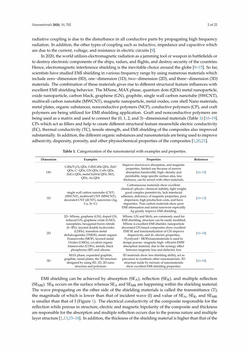
In 2020, the world utilizes electromagnetic radiation as a jamming tool or weapon in battlefields orto destroy electronic components of the ships, radars, and flights, and destroy security of the countries.Hence, electromagnetic interference shielding is the inevitable choice around the globe [9–15]. So far,scientists have studied EMI shielding in various frequency range by using numerous materials whichinclude zero−dimension (0D), one−dimension (1D), two−dimension (2D), and three−dimension (3D)materials. The combination of these materials gives rise to different structural feature influences withexcellent EMI shielding behavior. The MXene, MAX phase, quantum dots (QDs) metal nanoparticle,oxide nanoparticle, carbon black, graphene (GN), graphite, single wall carbon nanotube (SWCNT),multiwall carbon nanotube (MWCNT), magnetic nanoparticle, metal oxides, core shell Nano materials,metal plates, organic substances, nonconductive polymers (NCP), conductive polymers (CP), and craftpolymers are being utilized for EMI shielding application. Graft and nonconductive polymers arebeing used as a matrix and used to connect the (0, 1, 2, and 3)−dimensional materials (Table 1) [10–19].CPs which act as fillers and help to create different structural feature meanwhile electric conductivity(EC), thermal conductivity (TC), tensile strength, and EMI shielding of the composites also improvedsubstantially. In addition, the different organic substances and nanomaterials are being used to improveadhesivity, dispersity, porosity, and other physiochemical properties of the composites [1,20,21].
Table 1. Categorization of the nanomaterial with examples and properties.
Dimension Examples Properties Reference
OD
CdSe/V2O5 QDs, CdS/CdSe QDs, ZnOQDs, C−QDs, GN QDs, CoFe QDs,ZnCo QDs, metal hybrid QDs, SiO2
QDs, Au QDs
Improve microwave absorption, and magneticproperties, limited use because of narrowabsorption bandwidth, high−density andperishable, large specific surface area, less
thickness, can be mixed with other materials,
[10–15]
1D
single wall carbon nanotube (CNT)(SWCNT), multiwall CNT (MWCNT),
decorated CNT (dCNT), nanowires (Ag,Cu, Si−C)
Carbonaceous materials show excellentchemical−physio−chemical stability, light weight,
good complex permittivity, lack interfacialadhesion, deficiency of magnetic properties, poor
dispersion, high production costs, and haveimpurities. Pure carbon materials show poor
EMI attenuation and metal nanowire especiallyAg greatly improve EMI shielding.
[10–13]
2D
2D−MXene, graphene (GN), doped GN,reduced GN, graphene oxide (GNO),nanoplates, hexagonal boron nitride(h−BN), layered double hydroxides
(LDHs), transition metaldichalcogenides (TMDS), metal–organic
Frameworks (MOF), layered metalOxides (LMOs), covalent organicframeworks (COFs), metals, black
phosphorus (BP) and silicene
MXene, GN and MoS2 are commonly used forEMI shielding, structure can be easily modified,MXene is excellent EMI shielder, nanoparticle
decorated GN based composites show excellentEMI SE and functionalization of GN improve
dispersivity, and di−electric properties,Pyrolyzed−MOFs/nanomaterials is used to
design porous−magnetic high−efficient EMWabsorption material, due to the synergy effect
between magnetic loss and dielectric loss
[16–18]
3D
MAX phase, expanded graphite,graphite, metal plates, the 3D structure
designed by using 0D, 1D, 2D nanostructure and polymers
3D materials show less shielding ability, act asprecursor to synthesis other nanomaterials, 3D
structure made by mixture of nanomaterialsshow excellent EMI shielding properties.
[10–18]
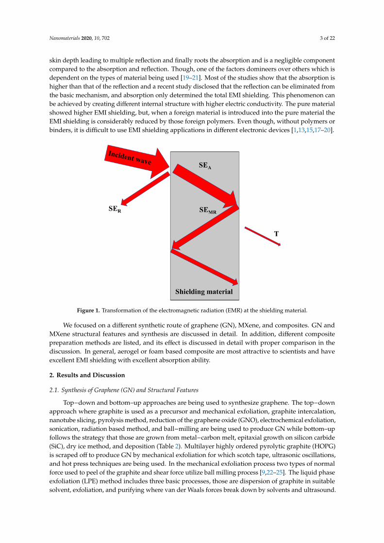
EMI shielding can be achieved by absorption (SEA), reflection (SER), and multiple reflection(SEMR). SER occurs on the surface whereas SEA and SEMR are happening within the shielding material.The wave propagating on the other side of the shielding materials is called the transmittance (T),the magnitude of which is lower than that of incident wave (I) and value of SEA, SER, and SEMR
is smaller than that of I (Figure 1). The electrical conductivity of the composite responsible for thereflection while porous in structure, electric and magnetic bipolarity of the composite and thicknessare responsible for the absorption and multiple reflection occurs due to the porous nature and multiplelayer structure [1,13,15–18]. In addition, the thickness of the shielding material is higher than that of the
Nanomaterials 2020, 10, 702 3 of 22
skin depth leading to multiple reflection and finally roots the absorption and is a negligible componentcompared to the absorption and reflection. Though, one of the factors domineers over others which isdependent on the types of material being used [19–21]. Most of the studies show that the absorption ishigher than that of the reflection and a recent study disclosed that the reflection can be eliminated fromthe basic mechanism, and absorption only determined the total EMI shielding. This phenomenon canbe achieved by creating different internal structure with higher electric conductivity. The pure materialshowed higher EMI shielding, but, when a foreign material is introduced into the pure material theEMI shielding is considerably reduced by those foreign polymers. Even though, without polymers orbinders, it is difficult to use EMI shielding applications in different electronic devices [1,13,15,17–20].
Nanomaterials 2020, 10, x FOR PEER REVIEW 3 of 23
covalent organic frameworks (COFs),
metals, black phosphorus (BP) and
silicene
Pyrolyzed− MOFs/ nanomaterials is used to
design porous−magnetic high−efficient
EMW absorption material, due to the
synergy effect between magnetic loss and
dielectric loss
3D
MAX phase, expanded graphite, graphite,
metal plates, the 3D structure designed
by using 0D, 1D, 2D nano structure and
polymers
3D materials show less shielding ability, act
as precursor to synthesis other
nanomaterials, 3D structure made by
mixture of nanomaterials show excellent
EMI shielding properties.
[10–18]
EMI shielding can be achieved by absorption (SEA), reflection (SER), and multiple reflection
(SEMR). SER occurs on the surface whereas SEA and SEMR are happening within the shielding material.
The wave propagating on the other side of the shielding materials is called the transmittance (T), the
magnitude of which is lower than that of incident wave (I) and value of SEA, SER, and SEMR is smaller
than that of I (Figure 1). The electrical conductivity of the composite responsible for the reflection
while porous in structure, electric and magnetic bipolarity of the composite and thickness are
responsible for the absorption and multiple reflection occurs due to the porous nature and multiple
layer structure [1,13,15–18]. In addition, the thickness of the shielding material is higher than that of
the skin depth leading to multiple reflection and finally roots the absorption and is a negligible
component compared to the absorption and reflection. Though, one of the factors domineers over
others which is dependent on the types of material being used [19–21]. Most of the studies show that
the absorption is higher than that of the reflection and a recent study disclosed that the reflection can
be eliminated from the basic mechanism, and absorption only determined the total EMI shielding.
This phenomenon can be achieved by creating different internal structure with higher electric
conductivity. The pure material showed higher EMI shielding, but, when a foreign material is
introduced into the pure material the EMI shielding is considerably reduced by those foreign
polymers. Even though, without polymers or binders, it is difficult to use EMI shielding applications
in different electronic devices [1,13,15,17–20].
Figure 1. Transformation of the electromagnetic radiation (EMR) at the shielding material. Figure 1. Transformation of the electromagnetic radiation (EMR) at the shielding material.
We focused on a different synthetic route of graphene (GN), MXene, and composites. GN andMXene structural features and synthesis are discussed in detail. In addition, different compositepreparation methods are listed, and its effect is discussed in detail with proper comparison in thediscussion. In general, aerogel or foam based composite are most attractive to scientists and haveexcellent EMI shielding with excellent absorption ability.
2. Results and Discussion
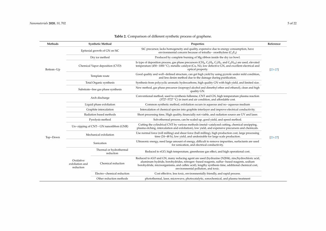
2.1. Synthesis of Graphene (GN) and Structural Features
Top−down and bottom–up approaches are being used to synthesize graphene. The top−downapproach where graphite is used as a precursor and mechanical exfoliation, graphite intercalation,nanotube slicing, pyrolysis method, reduction of the graphene oxide (GNO), electrochemical exfoliation,sonication, radiation based method, and ball−milling are being used to produce GN while bottom–upfollows the strategy that those are grown from metal−carbon melt, epitaxial growth on silicon carbide(SiC), dry ice method, and deposition (Table 2). Multilayer highly ordered pyrolytic graphite (HOPG)is scraped off to produce GN by mechanical exfoliation for which scotch tape, ultrasonic oscillations,and hot press techniques are being used. In the mechanical exfoliation process two types of normalforce used to peel of the graphite and shear force utilize ball milling process [9,22–25]. The liquid phaseexfoliation (LPE) method includes three basic processes, those are dispersion of graphite in suitablesolvent, exfoliation, and purifying where van der Waals forces break down by solvents and ultrasound.
Nanomaterials 2020, 10, 702 4 of 22
The arc discharge method is utilized to synthesize the allotropes of carbon such as graphene, CNT, andfullerene. In which, the carbon precursor is used as the anode and the graphite rod as the cathode,where applied electrical current creates the plasma at higher temperature (3727–5727 C) and finallyform graphene. Various intercalants are being utilized by the intercalation technique. By carbonnanotube (CNT) slicing/unzipping micron size GN are produced for which plasma or chemical etching,intercalation and exfoliation, metal catalyst cutting, abrade on the glass surface, and the CNT tubeopens into a lay-flat single layer graphene ribbon (GNR). The pyrolysis is the type of the solvothermaltechnique where equal molar sodium and ethanol are used to separate the graphite layers. Thethermal annealing technique is where amorphous carbon is converted into single layer grapheneon the nickel and cobalt surface with the aid of temperature. The reduction of the graphene oxide(GO) can be performed by using chemicals, biomass, radiation, bacteria, electrochemical methods,and heat treatment. Electrochemical exfoliation is practiced in an acidic environment by applyingvoltage differences between the anode (graphite) and cathode (platinum) while solvent-based highenergy is used in the sonication technique. The ball milling utilized solvent or chemical assistance andmagnetic assistance technique, although higher quality GN are being produced by using radiationtechniques. Laser and electron beams are used in radiation techniques. The deposition method utilizesthe Chemical Vapor Deposition (CVD) techniques where solid, liquid, and gaseous carbon precursorsare being used, filtration with reduction, spin coating, and spray coating process for GN synthesis. TheCVD produces graphene with low defects and during the process the precursors are atomized, and thegraphene is formed on the metal catalyst (Cu and Ni). The epitaxial growth is performed on a siliconcarbide wafer where stacks of graphene are formed. The epitaxial growth is the exothermic processduring which the sublimated (1200–1600 C) silicon leaves excessive sp2 hybridized carbon networkformed graphene. In addition, burning the dry ice by using magnesium followed by acid treatmentproduces GN (Table 2) [9,23–27].
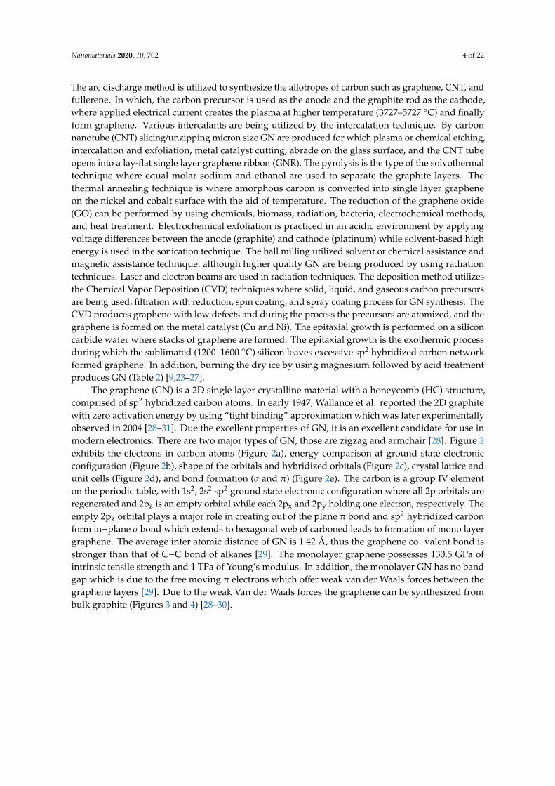
The graphene (GN) is a 2D single layer crystalline material with a honeycomb (HC) structure,comprised of sp2 hybridized carbon atoms. In early 1947, Wallance et al. reported the 2D graphitewith zero activation energy by using “tight binding” approximation which was later experimentallyobserved in 2004 [28–31]. Due the excellent properties of GN, it is an excellent candidate for use inmodern electronics. There are two major types of GN, those are zigzag and armchair [28]. Figure 2exhibits the electrons in carbon atoms (Figure 2a), energy comparison at ground state electronicconfiguration (Figure 2b), shape of the orbitals and hybridized orbitals (Figure 2c), crystal lattice andunit cells (Figure 2d), and bond formation (σ and π) (Figure 2e). The carbon is a group IV elementon the periodic table, with 1s2, 2s2 sp2 ground state electronic configuration where all 2p orbitals areregenerated and 2pz is an empty orbital while each 2px and 2py holding one electron, respectively. Theempty 2pz orbital plays a major role in creating out of the plane π bond and sp2 hybridized carbonform in−plane σ bond which extends to hexagonal web of carboned leads to formation of mono layergraphene. The average inter atomic distance of GN is 1.42 Å, thus the graphene co−valent bond isstronger than that of C−C bond of alkanes [29]. The monolayer graphene possesses 130.5 GPa ofintrinsic tensile strength and 1 TPa of Young’s modulus. In addition, the monolayer GN has no bandgap which is due to the free moving π electrons which offer weak van der Waals forces between thegraphene layers [29]. Due to the weak Van der Waals forces the graphene can be synthesized frombulk graphite (Figures 3 and 4) [28–30].
Nanomaterials 2020, 10, 702 5 of 22
Table 2. Comparison of different synthetic process of graphene.
Methods Synthetic Method Properties Reference
Bottom−Up
Epitaxial growth of GN on SiC SiC precursor, lacks homogeneity and quality, expensive due to energy consumption, haveenvironmental concern because of tetraflu− oroethylene (C2F4)
[23–27]
Dry ice method Produced by complete burning of Mg ribbon inside the dry ice bowl.
Chemical Vapor deposition (CVD)Is type of deposition process, gas phase precursors (CH4, C2H4, C2H2, and C6H14) are used, elevatedtemperature (450−1000 C), metallic catalyst (Cu, Ni), low defective GN, and excellent electrical and
optical property.
Template route Good quality and well−defined structure, can get high yield by using pyrrole under mild condition,and less desire method due to the damage during purification.
Total Organic synthesis Synthesis from polycyclic aromatic hydrocarbons, high quality GN with high yield, and limited size.
Substrate−free gas phase synthesis New method, gas phase precursor (isopropyl alcohol and dimethyl ether and ethanol), clean and highquality GN.
Top−Down
Arch discharge Conventional method, used to synthesis fullerene, CNT and GN, high temperature plasma reaction(3727–5727 C) in inert and air condition, and affordable cost.
[23–27]
Liquid phase exfoliation Common synthetic method, exfoliation occurs in aqueous and no−aqueous medium
Graphite intercalation Intercalation of chemical species into graphite interlayer and improve electrical conductivity.
Radiation based methods Short processing time, High quality, financially not viable, and radiation source are UV and laser.
Pyrolysis method Solvothermal process, can be scaled up, good yield, and speed method.
Un−zipping of CNT− GN nanoribbon (GNR) Cutting the cylindrical CNT by various methods (metal−catalyzed cutting, chemical unzipping,plasma etching, intercalation and exfoliation), low yield, and expensive precursors and chemicals.
Mechanical exfoliation Use normal force (roll milling) and shear force (ball milling), high production cost, large processingtime (24−48 h), low yield, and undesirable for large scale production.
Sonication Ultrasonic energy, need large amount of energy, difficult to remove impurities, surfactants are usedfor sonication, and electrical conductivity.
Oxidativeexfoliation and
reduction
Thermal or hydrothermalreduction Reduced to rGO, high temperature, greenhouse gas effect, and high operational cost.
Chemical reduction
Reduced to rGO and GN, many reducing agent are used (hydrazine (N2H4), zinc/hydrochloric acid,aluminum hydride, borohydrides, nitrogen−based reagents, sulfur−based reagents, sodium
borohydride, microorganisms, and caffeic acid), lengthy synthesis time, additional chemical cost,environmental pollution, and toxic.
Electro−chemical reduction Cost effective, less toxic, environmentally friendly, and rapid process.
Other reduction methods photothermal, laser, microwave, photocatalytic, sonochemical, and plasma treatment
Nanomaterials 2020, 10, 702 6 of 22Nanomaterials 2020, 10, x FOR PEER REVIEW 7 of 23
Figure 2. (a). Atomic structure of a carbon atom. (b) Energy levels of outer electrons in carbon atoms.
(c) The formation of sp2 hybrids. (d) The crystal lattice of graphene, where A and B are carbon atoms
belonging to different sub−lattices, a1 and a2 are unit−cell vectors. (e) Sigma bond and pi bond formed
by sp2 hybridization [29] Copyright Science and technology of advanced materials, 2018.
Figure 3. Zigzag–edged and armchair–edged of graphene (GNs).
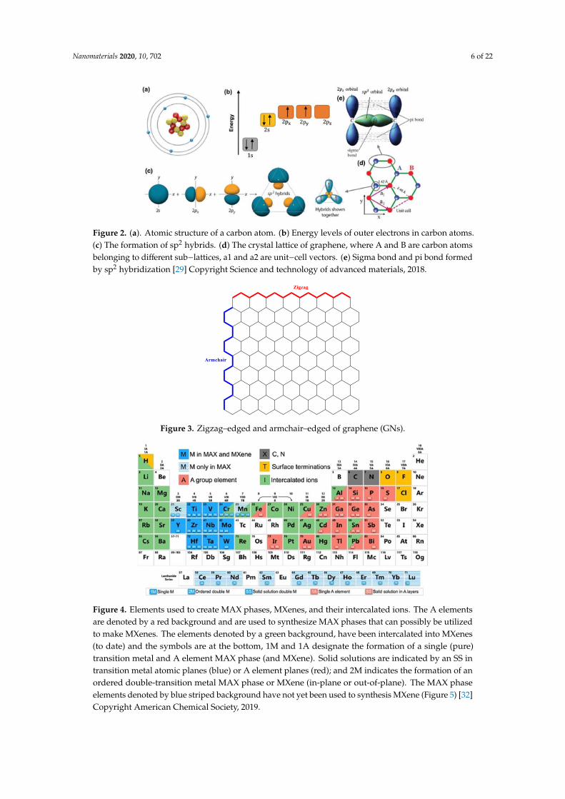
2.2. MXene Synthesis and Structural Features.
The MXene is a fast-growing two−dimensional (2D) material, derived from its corresponding 3D
MAX phase by an etching process. The general formula of MXene is Mn+1XnTx where M is an early
transition element, n = 1–3, X is a carbon or nitrogen and Tx is a surface functional groups −F, −OH,
=O, and Cl, which are directly attached to the M. The Mn+1AXn is used to denote the MAX phase where
generally is group A 13/14 element, but, several other elements also utilize for A layer (Figure 4 and
Table 1). The different combination of elements has been used for both MAX and MXene synthesis
shown below in Figures 5 and 6. The number of layers in MXene is determined by n where the n+1
layer of MXene is formed which is true for the MAX phase as well (Figure 5) [31–33].
Figure 2. (a). Atomic structure of a carbon atom. (b) Energy levels of outer electrons in carbon atoms.(c) The formation of sp2 hybrids. (d) The crystal lattice of graphene, where A and B are carbon atomsbelonging to different sub−lattices, a1 and a2 are unit−cell vectors. (e) Sigma bond and pi bond formedby sp2 hybridization [29] Copyright Science and technology of advanced materials, 2018.
Nanomaterials 2020, 10, x FOR PEER REVIEW 7 of 23
Figure 2. (a). Atomic structure of a carbon atom. (b) Energy levels of outer electrons in carbon atoms.
(c) The formation of sp2 hybrids. (d) The crystal lattice of graphene, where A and B are carbon atoms
belonging to different sub−lattices, a1 and a2 are unit−cell vectors. (e) Sigma bond and pi bond formed
by sp2 hybridization [29] Copyright Science and technology of advanced materials, 2018.
Figure 3. Zigzag–edged and armchair–edged of graphene (GNs).
2.2. MXene Synthesis and Structural Features.
The MXene is a fast-growing two−dimensional (2D) material, derived from its corresponding 3D
MAX phase by an etching process. The general formula of MXene is Mn+1XnTx where M is an early
transition element, n = 1–3, X is a carbon or nitrogen and Tx is a surface functional groups −F, −OH,
=O, and Cl, which are directly attached to the M. The Mn+1AXn is used to denote the MAX phase where
generally is group A 13/14 element, but, several other elements also utilize for A layer (Figure 4 and
Table 1). The different combination of elements has been used for both MAX and MXene synthesis
shown below in Figures 5 and 6. The number of layers in MXene is determined by n where the n+1
layer of MXene is formed which is true for the MAX phase as well (Figure 5) [31–33].
Figure 3. Zigzag–edged and armchair–edged of graphene (GNs).Nanomaterials 2020, 10, x FOR PEER REVIEW 8 of 23
Figure 4. Elements used to create MAX phases, MXenes, and their intercalated ions. The A
elements are denoted by a red background and are used to synthesize MAX phases that can
possibly be utilized to make MXenes. The elements denoted by a green background, have
been intercalated into MXenes (to date) and the symbols are at the bottom, 1M and 1A
designate the formation of a single (pure) transition metal and A element MAX phase (and
MXene). Solid solutions are indicated by an SS in transition metal atomic planes (blue) or A
element planes (red); and 2M indicates the formation of an ordered double-transition metal
MAX phase or MXene (in-plane or out-of-plane). The MAX phase elements denoted by blue
striped background have not yet been used to synthesis MXene (Figure 5) [32] Copyright
American Chemical Society, 2019.
Figure 4. Elements used to create MAX phases, MXenes, and their intercalated ions. The A elementsare denoted by a red background and are used to synthesize MAX phases that can possibly be utilizedto make MXenes. The elements denoted by a green background, have been intercalated into MXenes(to date) and the symbols are at the bottom, 1M and 1A designate the formation of a single (pure)transition metal and A element MAX phase (and MXene). Solid solutions are indicated by an SS intransition metal atomic planes (blue) or A element planes (red); and 2M indicates the formation of anordered double-transition metal MAX phase or MXene (in-plane or out-of-plane). The MAX phaseelements denoted by blue striped background have not yet been used to synthesis MXene (Figure 5) [32]Copyright American Chemical Society, 2019.
Nanomaterials 2020, 10, 702 7 of 22
Nanomaterials 2020, 10, x FOR PEER REVIEW 8 of 23
Figure 4. Elements used to create MAX phases, MXenes, and their intercalated ions. The A
elements are denoted by a red background and are used to synthesize MAX phases that can
possibly be utilized to make MXenes. The elements denoted by a green background, have
been intercalated into MXenes (to date) and the symbols are at the bottom, 1M and 1A
designate the formation of a single (pure) transition metal and A element MAX phase (and
MXene). Solid solutions are indicated by an SS in transition metal atomic planes (blue) or A
element planes (red); and 2M indicates the formation of an ordered double-transition metal
MAX phase or MXene (in-plane or out-of-plane). The MAX phase elements denoted by blue
striped background have not yet been used to synthesis MXene (Figure 5) [32] Copyright
American Chemical Society, 2019.
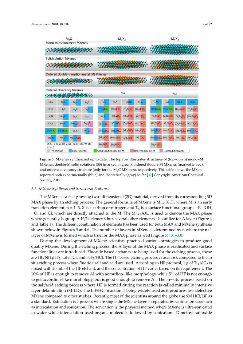
Figure 5. MXenes synthesized up to date. The top row illustrates structures of (top–down) mono−MMXenes, double-M solid solutions (SS) (marked in green), ordered double-M MXenes (marked in red),and ordered divacancy structure (only for the M2C MXenes), respectively. This table shows the MXenereported both experimentally (blue) and theoretically (gray) so far [32] Copyright American ChemicalSociety, 2019.
2.2. MXene Synthesis and Structural Features.
The MXene is a fast-growing two−dimensional (2D) material, derived from its corresponding 3DMAX phase by an etching process. The general formula of MXene is Mn+1XnTx where M is an earlytransition element, n = 1–3, X is a carbon or nitrogen and Tx is a surface functional groups −F, −OH,=O, and Cl, which are directly attached to the M. The Mn+1AXn is used to denote the MAX phasewhere generally is group A 13/14 element, but, several other elements also utilize for A layer (Figure 4and Table 1). The different combination of elements has been used for both MAX and MXene synthesisshown below in Figures 5 and 6. The number of layers in MXene is determined by n where the n+1layer of MXene is formed which is true for the MAX phase as well (Figure 5) [31–33].
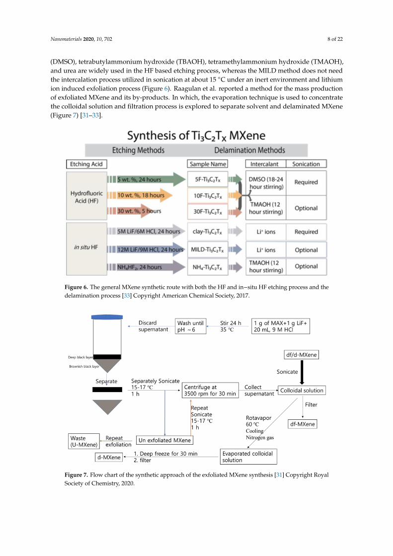
During the development of MXene scientists practiced various strategies to produce goodquality MXene. During the etching process, the A layer of the MAX phase is eradicated and surfacefunctionalities are introduced. Fluoride based etchants are being used for the etching process, thoseare HF, NH4HF2, LiF/HCl, and FeF3/HCl. The HF based etching process causes risk compared to the insitu etching process where fluoride salt and acid are used. According to HF protocol, 1 g of Ti3AlC2 ismixed with 20 mL of the HF etchant, and the concentration of HF varies based on its requirement. The10% of HF is enough to remove Al with accordion−like morphology while 5% of HF is not enoughto get accordion-like morphology, but is good enough to remove Al. The in−situ process based onthe salt/acid etching process where HF is formed during the reaction is called minimally intensivelayer delamination (MILD). The LiF/HCl reaction is being widely used as it produces less defectiveMXene compared to other studies. Recently, most of the scientists around the globe use 9M HCl/LiF asa standard. Exfoliation is a process where single the MXene layer is separated by various process suchas intercalation and sonication. The sonication is the physical method where MXene is ultra-sonicatedin water while intercalation used organic molecules followed by sonication. Dimethyl sulfoxide
Nanomaterials 2020, 10, 702 8 of 22
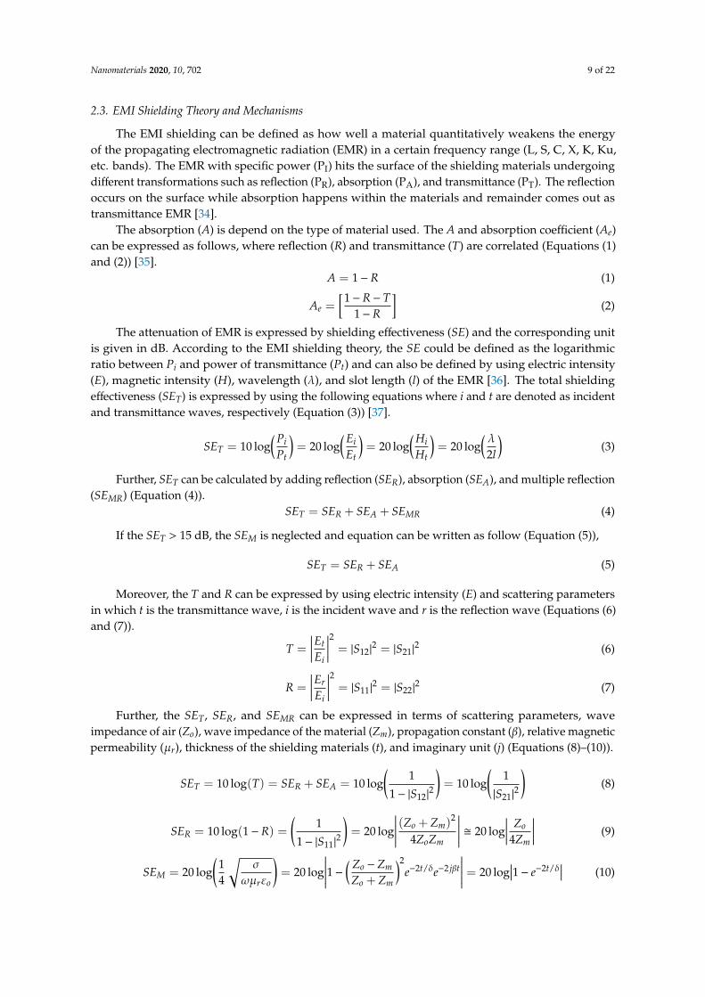
(DMSO), tetrabutylammonium hydroxide (TBAOH), tetramethylammonium hydroxide (TMAOH),and urea are widely used in the HF based etching process, whereas the MILD method does not needthe intercalation process utilized in sonication at about 15 C under an inert environment and lithiumion induced exfoliation process (Figure 6). Raagulan et al. reported a method for the mass productionof exfoliated MXene and its by-products. In which, the evaporation technique is used to concentratethe colloidal solution and filtration process is explored to separate solvent and delaminated MXene(Figure 7) [31–33].
Nanomaterials 2020, 10, x FOR PEER REVIEW 9 of 23
Figure 5. MXenes synthesized up to date. The top row illustrates structures of (top–down) mono−M
MXenes, double-M solid solutions (SS) (marked in green), ordered double-M MXenes (marked in red),
and ordered divacancy structure (only for the M2C MXenes), respectively. This table shows the MXene
reported both experimentally (blue) and theoretically (gray) so far [32] Copyright American Chemical
Society, 2019.
During the development of MXene scientists practiced various strategies to produce good
quality MXene. During the etching process, the A layer of the MAX phase is eradicated and surface
functionalities are introduced. Fluoride based etchants are being used for the etching process, those
are HF, NH4HF2, LiF/HCl, and FeF3/HCl. The HF based etching process causes risk compared to the
in situ etching process where fluoride salt and acid are used. According to HF protocol, 1 g of Ti3AlC2
is mixed with 20 mL of the HF etchant, and the concentration of HF varies based on its requirement.
The 10% of HF is enough to remove Al with accordion−like morphology while 5% of HF is not enough
to get accordion-like morphology, but is good enough to remove Al. The in−situ process based on the
salt/acid etching process where HF is formed during the reaction is called minimally intensive layer
delamination (MILD). The LiF/HCl reaction is being widely used as it produces less defective MXene
compared to other studies. Recently, most of the scientists around the globe use 9M HCl/LiF as a
standard. Exfoliation is a process where single the MXene layer is separated by various process such
as intercalation and sonication. The sonication is the physical method where MXene is ultra-sonicated
in water while intercalation used organic molecules followed by sonication. Dimethyl sulfoxide
(DMSO), tetrabutylammonium hydroxide (TBAOH), tetramethylammonium hydroxide (TMAOH),
and urea are widely used in the HF based etching process, whereas the MILD method does not need
the intercalation process utilized in sonication at about 15 under an inert environment and lithium
ion induced exfoliation process (Figure 6). Raagulan et al. reported a method for the mass production
of exfoliated MXene and its by-products. In which, the evaporation technique is used to concentrate
the colloidal solution and filtration process is explored to separate solvent and delaminated MXene
(Figure 7) [31–33]
Figure 6. The general MXene synthetic route with both the HF and in−situ HF etching process and
the delamination process [33] Copyright American Chemical Society, 2017. Figure 6. The general MXene synthetic route with both the HF and in−situ HF etching process and thedelamination process [33] Copyright American Chemical Society, 2017.
Nanomaterials 2020, 10, x FOR PEER REVIEW 10 of 23
Figure 7. Flow chart of the synthetic approach of the exfoliated MXene synthesis [31] Copyright Royal
Society of Chemistry, 2020.
2.3. EMI Shielding Theory and Mechanisms
The EMI shielding can be defined as how well a material quantitatively weakens the energy of
the propagating electromagnetic radiation (EMR) in a certain frequency range (L, S, C, X, K, Ku, etc.
bands). The EMR with specific power (PI) hits the surface of the shielding materials undergoing
different transformations such as reflection (PR), absorption (PA), and transmittance (PT). The
reflection occurs on the surface while absorption happens within the materials and remainder comes
out as transmittance EMR [34].
The absorption (A) is depend on the type of material used. The A and absorption coefficient (Ae)
can be expressed as follows, where reflection (R) and transmittance (T) are correlated (Equations 1
and 2) [35].
A = 1 − R (1)
𝐴𝑒 = [1 − 𝑅 − 𝑇
1 − 𝑅] (2)
The attenuation of EMR is expressed by shielding effectiveness (SE) and the corresponding unit
is given in dB. According to the EMI shielding theory, the SE could be defined as the logarithmic ratio
between Pi and power of transmittance (Pt) and can also be defined by using electric intensity (E),
magnetic intensity (H), wavelength (λ), and slot length (l) of the EMR [36]. The total shielding
effectiveness (SET) is expressed by using the following equations where i and t are denoted as incident
and transmittance waves, respectively (Equation 3) [37].
𝑆𝐸𝑇 = 10𝑙𝑜𝑔 (𝑃𝑖
𝑃𝑡) = 20𝑙𝑜𝑔 (
𝐸𝑖
𝐸𝑡) = 20𝑙𝑜𝑔 (
𝐻𝑖
𝐻𝑡) = 20𝑙𝑜𝑔 (
𝜆
2𝑙) (3)
Further, SET can be calculated by adding reflection (SER), absorption (SEA), and multiple
reflection (SEMR) (Equation 4).
𝑆𝐸𝑇 = 𝑆𝐸𝑅 + 𝑆𝐸𝐴 + 𝑆𝐸𝑀𝑅 (4)
If the SET > 15 dB, the SEM is neglected and equation can be written as follow (Equation 5),
𝑆𝐸𝑇 = 𝑆𝐸𝑅 + 𝑆𝐸𝐴 (5)
Moreover, the T and R can be expressed by using electric intensity (E) and scattering parameters
in which t is the transmittance wave, i is the incident wave and r is the reflection wave (Equations 6
and 7).
Figure 7. Flow chart of the synthetic approach of the exfoliated MXene synthesis [31] Copyright RoyalSociety of Chemistry, 2020.
Nanomaterials 2020, 10, 702 9 of 22
2.3. EMI Shielding Theory and Mechanisms
The EMI shielding can be defined as how well a material quantitatively weakens the energyof the propagating electromagnetic radiation (EMR) in a certain frequency range (L, S, C, X, K, Ku,etc. bands). The EMR with specific power (PI) hits the surface of the shielding materials undergoingdifferent transformations such as reflection (PR), absorption (PA), and transmittance (PT). The reflectionoccurs on the surface while absorption happens within the materials and remainder comes out astransmittance EMR [34].
The absorption (A) is depend on the type of material used. The A and absorption coefficient (Ae)can be expressed as follows, where reflection (R) and transmittance (T) are correlated (Equations (1)and (2)) [35].
A = 1−R (1)
Ae =[1−R− T
1−R
](2)
The attenuation of EMR is expressed by shielding effectiveness (SE) and the corresponding unitis given in dB. According to the EMI shielding theory, the SE could be defined as the logarithmicratio between Pi and power of transmittance (Pt) and can also be defined by using electric intensity(E), magnetic intensity (H), wavelength (λ), and slot length (l) of the EMR [36]. The total shieldingeffectiveness (SET) is expressed by using the following equations where i and t are denoted as incidentand transmittance waves, respectively (Equation (3)) [37].
SET = 10 log(Pi
Pt
)= 20 log
(EiEt
)= 20 log
(HiHt
)= 20 log
(λ2l
)(3)
Further, SET can be calculated by adding reflection (SER), absorption (SEA), and multiple reflection(SEMR) (Equation (4)).
SET = SER + SEA + SEMR (4)
If the SET > 15 dB, the SEM is neglected and equation can be written as follow (Equation (5)),
SET = SER + SEA (5)
Moreover, the T and R can be expressed by using electric intensity (E) and scattering parametersin which t is the transmittance wave, i is the incident wave and r is the reflection wave (Equations (6)and (7)).
T =
∣∣∣∣∣Et
Ei
∣∣∣∣∣2 = |S12|2 = |S21|
2 (6)
R =
∣∣∣∣∣Er
Ei
∣∣∣∣∣2 = |S11|2 = |S22|
2 (7)
Further, the SET, SER, and SEMR can be expressed in terms of scattering parameters, waveimpedance of air (Zo), wave impedance of the material (Zm), propagation constant (β), relative magneticpermeability (µr), thickness of the shielding materials (t), and imaginary unit (j) (Equations (8)–(10)).
SET = 10 log(T) = SER + SEA = 10 log(
1
1− |S12|2
)= 10 log
(1
|S21|2
)(8)
SER = 10 log(1−R) =(
1
1− |S11|2
)= 20 log
∣∣∣∣∣∣ (Zo + Zm)2
4ZoZm
∣∣∣∣∣∣ 20 log∣∣∣∣∣ Zo
4Zm
∣∣∣∣∣ (9)
SEM = 20 log(
14
√σ
ωµrεo
)= 20 log
∣∣∣∣∣∣1− ( Zo −Zm
Zo + Zm
)2e−2t/δe−2 jβt
∣∣∣∣∣∣ = 20 log∣∣∣1− e−2t/δ
∣∣∣ (10)
Nanomaterials 2020, 10, 702 10 of 22
In addition, the SEA, SER, and SEMR can differently be described by using parameters of the
shielding materials such as t, skin depth (
Nanomaterials 2020, 10, x FOR PEER REVIEW 11 of 23
T = 𝐸𝐸 = |𝑆 | = |𝑆 | (6)
R = 𝐸𝐸 = |𝑆 | = |𝑆 | (7)
Further, the SET, SER, and SEMR can be expressed in terms of scattering parameters, wave impedance of air (Zo), wave impedance of the material (Zm), propagation constant (β), relative magnetic permeability (μr), thickness of the shielding materials (t), and imaginary unit (j) (Equations 8–10). 𝑆𝐸 = 10 log(T) = 𝑆𝐸 + 𝑆𝐸 = 10𝑙𝑜𝑔 11 − |𝑆 | = 10𝑙𝑜𝑔 1|𝑆 | (8)
𝑆𝐸 = 10log(1 − 𝑅) = 11 − |𝑆 | = 20 𝑙𝑜𝑔 (𝑍 + 𝑍 )4𝑍 𝑍 ≅ 20𝑙𝑜𝑔 𝑍4𝑍 (9)
𝑆𝐸 = 20log 14 𝜎𝜔𝜇 𝜀 = 20 log 1 − 𝑍 − 𝑍𝑍 + 𝑍 𝑒 ⁄ 𝑒 = 20𝑙𝑜𝑔 1 − 𝑒 ⁄ (10)
In addition, the SEA, SER, and SEMR can differently be described by using parameters of the shielding materials such as t, skin depth ( ), μr, refractive index (n), relative conductivity (бr), and imaginary part of wave vector (ik) (Equations 11–13). 𝑆𝐸 = 8.7𝑡 = 131.4d 𝑓𝜇 𝜎 = 𝐾 𝑡𝛿 = 10𝑙𝑜𝑔 𝑇(1 − 𝑅) = 10𝑙𝑜𝑔(1 − 𝐴 ) = 20𝑙𝑜𝑔𝑒 ⁄
= 20𝑙𝑚(𝑘)𝑑 𝑙𝑜𝑔 𝑒 (11)
𝑆𝐸 = 108 + log 𝜎𝑓𝜇 = 39.5 + 10𝑙𝑜𝑔 𝜎2𝜋𝑓𝜇 = 20𝑙𝑜𝑔 1 + 𝑛4𝑛 (12)
𝑆𝐸 = 20log 1 − 10 = 168 + 10𝑙𝑜𝑔 𝜎𝜇𝑓 = 20𝑙𝑜𝑔 1 − (1 − 𝑛 )(1 + 𝑛) exp (2𝑖𝑘𝑑) (13)
Skin depth is inversely proportional to square root of πfбμ of the composition where f is frequency of EMR, μ is magnetic permeability, and б is electric conductivity (Equation 14) [36]. = 1𝜋𝑓𝜎𝜇 (14)
When the electromagnetic radiation propagates, it undergoes the changes from near field to far field which is depend on the distance. The r < λ/2π is considered as near field and r > λ/2π is denoted as far field. Thus, most of the EMRs are far field and are regarded as planar waves. The impedance of the wave (intrinsic impedance) Z can be articulated that the amplitude ratio between electric fielding (E) and magnetic field (H) waves, which are perpendicular to each other (E H). Furthermore, the Z is influenced by б, μ, angular frequency (ω = 2πf), j, and electric permeability (ε).
Z of air is symbolized as Zo, and has a value of 377 Ω and at this stage j and ω is considered as one
and б is zero (Equations 15–17). Z = |𝐸||𝐻| (15)
Z = 𝑗𝜔𝜇𝜎 − 𝑗𝜔𝜀 (16)
𝑍 = 𝜇𝜀 (17)
), µr, refractive index (n), relative conductivity (σr), andimaginary part of wave vector (ik) (Equations (11)–(13)).
SEA = 8.7t
Nanomaterials 2020, 10, x FOR PEER REVIEW 11 of 23
T = 𝐸𝐸 = |𝑆 | = |𝑆 | (6)
R = 𝐸𝐸 = |𝑆 | = |𝑆 | (7)
Further, the SET, SER, and SEMR can be expressed in terms of scattering parameters, wave impedance of air (Zo), wave impedance of the material (Zm), propagation constant (β), relative magnetic permeability (μr), thickness of the shielding materials (t), and imaginary unit (j) (Equations 8–10). 𝑆𝐸 = 10 log(T) = 𝑆𝐸 + 𝑆𝐸 = 10𝑙𝑜𝑔 11 − |𝑆 | = 10𝑙𝑜𝑔 1|𝑆 | (8)
𝑆𝐸 = 10log(1 − 𝑅) = 11 − |𝑆 | = 20 𝑙𝑜𝑔 (𝑍 + 𝑍 )4𝑍 𝑍 ≅ 20𝑙𝑜𝑔 𝑍4𝑍 (9)
𝑆𝐸 = 20log 14 𝜎𝜔𝜇 𝜀 = 20 log 1 − 𝑍 − 𝑍𝑍 + 𝑍 𝑒 ⁄ 𝑒 = 20𝑙𝑜𝑔 1 − 𝑒 ⁄ (10)
In addition, the SEA, SER, and SEMR can differently be described by using parameters of the shielding materials such as t, skin depth ( ), μr, refractive index (n), relative conductivity (бr), and imaginary part of wave vector (ik) (Equations 11–13). 𝑆𝐸 = 8.7𝑡 = 131.4d 𝑓𝜇 𝜎 = 𝐾 𝑡𝛿 = 10𝑙𝑜𝑔 𝑇(1 − 𝑅) = 10𝑙𝑜𝑔(1 − 𝐴 ) = 20𝑙𝑜𝑔𝑒 ⁄
= 20𝑙𝑚(𝑘)𝑑 𝑙𝑜𝑔 𝑒 (11)
𝑆𝐸 = 108 + log 𝜎𝑓𝜇 = 39.5 + 10𝑙𝑜𝑔 𝜎2𝜋𝑓𝜇 = 20𝑙𝑜𝑔 1 + 𝑛4𝑛 (12)
𝑆𝐸 = 20log 1 − 10 = 168 + 10𝑙𝑜𝑔 𝜎𝜇𝑓 = 20𝑙𝑜𝑔 1 − (1 − 𝑛 )(1 + 𝑛) exp (2𝑖𝑘𝑑) (13)
Skin depth is inversely proportional to square root of πfбμ of the composition where f is frequency of EMR, μ is magnetic permeability, and б is electric conductivity (Equation 14) [36]. = 1𝜋𝑓𝜎𝜇 (14)
When the electromagnetic radiation propagates, it undergoes the changes from near field to far field which is depend on the distance. The r < λ/2π is considered as near field and r > λ/2π is denoted as far field. Thus, most of the EMRs are far field and are regarded as planar waves. The impedance of the wave (intrinsic impedance) Z can be articulated that the amplitude ratio between electric fielding (E) and magnetic field (H) waves, which are perpendicular to each other (E H). Furthermore, the Z is influenced by б, μ, angular frequency (ω = 2πf), j, and electric permeability (ε).
Z of air is symbolized as Zo, and has a value of 377 Ω and at this stage j and ω is considered as one
and б is zero (Equations 15–17). Z = |𝐸||𝐻| (15)
Z = 𝑗𝜔𝜇𝜎 − 𝑗𝜔𝜀 (16)
𝑍 = 𝜇𝜀 (17)
= 131.4d√
fµrσr = K(
tδ
)= 10 log
[T
(1−R)
]= 10 log(1−Ae) = 20 log et/δ = 20lm(k)d log e (11)
SER = 108 + log(σfµ
)= 39.5 + 10 log
(σ
2π fµ
)= 20 log
∣∣∣∣∣∣1 + n2
4n
∣∣∣∣∣∣ (12)
SEM = 20 log∣∣∣∣∣1− 10
SEA10
∣∣∣∣∣ = 168 + 10 log(σr
µ f
)= 20 log
∣∣∣∣∣∣∣1−(1− n2
)(1 + n)2 exp(2ikd)
∣∣∣∣∣∣∣ (13)
Skin depth is inversely proportional to square root of πfσµ of the composition where f is frequencyof EMR, µ is magnetic permeability, and σ is electric conductivity (Equation (14)) [36].
Nanomaterials 2020, 10, x FOR PEER REVIEW 11 of 23
T = 𝐸𝐸 = |𝑆 | = |𝑆 | (6)
R = 𝐸𝐸 = |𝑆 | = |𝑆 | (7)
Further, the SET, SER, and SEMR can be expressed in terms of scattering parameters, wave impedance of air (Zo), wave impedance of the material (Zm), propagation constant (β), relative magnetic permeability (μr), thickness of the shielding materials (t), and imaginary unit (j) (Equations 8–10). 𝑆𝐸 = 10 log(T) = 𝑆𝐸 + 𝑆𝐸 = 10𝑙𝑜𝑔 11 − |𝑆 | = 10𝑙𝑜𝑔 1|𝑆 | (8)
𝑆𝐸 = 10log(1 − 𝑅) = 11 − |𝑆 | = 20 𝑙𝑜𝑔 (𝑍 + 𝑍 )4𝑍 𝑍 ≅ 20𝑙𝑜𝑔 𝑍4𝑍 (9)
𝑆𝐸 = 20log 14 𝜎𝜔𝜇 𝜀 = 20 log 1 − 𝑍 − 𝑍𝑍 + 𝑍 𝑒 ⁄ 𝑒 = 20𝑙𝑜𝑔 1 − 𝑒 ⁄ (10)
In addition, the SEA, SER, and SEMR can differently be described by using parameters of the shielding materials such as t, skin depth ( ), μr, refractive index (n), relative conductivity (бr), and imaginary part of wave vector (ik) (Equations 11–13). 𝑆𝐸 = 8.7𝑡 = 131.4d 𝑓𝜇 𝜎 = 𝐾 𝑡𝛿 = 10𝑙𝑜𝑔 𝑇(1 − 𝑅) = 10𝑙𝑜𝑔(1 − 𝐴 ) = 20𝑙𝑜𝑔𝑒 ⁄
= 20𝑙𝑚(𝑘)𝑑 𝑙𝑜𝑔 𝑒 (11)
𝑆𝐸 = 108 + log 𝜎𝑓𝜇 = 39.5 + 10𝑙𝑜𝑔 𝜎2𝜋𝑓𝜇 = 20𝑙𝑜𝑔 1 + 𝑛4𝑛 (12)
𝑆𝐸 = 20log 1 − 10 = 168 + 10𝑙𝑜𝑔 𝜎𝜇𝑓 = 20𝑙𝑜𝑔 1 − (1 − 𝑛 )(1 + 𝑛) exp (2𝑖𝑘𝑑) (13)
Skin depth is inversely proportional to square root of πfбμ of the composition where f is frequency of EMR, μ is magnetic permeability, and б is electric conductivity (Equation 14) [36]. = 1𝜋𝑓𝜎𝜇 (14)
When the electromagnetic radiation propagates, it undergoes the changes from near field to far field which is depend on the distance. The r < λ/2π is considered as near field and r > λ/2π is denoted as far field. Thus, most of the EMRs are far field and are regarded as planar waves. The impedance of the wave (intrinsic impedance) Z can be articulated that the amplitude ratio between electric fielding (E) and magnetic field (H) waves, which are perpendicular to each other (E H). Furthermore, the Z is influenced by б, μ, angular frequency (ω = 2πf), j, and electric permeability (ε).
Z of air is symbolized as Zo, and has a value of 377 Ω and at this stage j and ω is considered as one
and б is zero (Equations 15–17). Z = |𝐸||𝐻| (15)
Z = 𝑗𝜔𝜇𝜎 − 𝑗𝜔𝜀 (16)
𝑍 = 𝜇𝜀 (17)
=1√π fσµ
(14)
When the electromagnetic radiation propagates, it undergoes the changes from near field to farfield which is depend on the distance. The r < λ/2π is considered as near field and r > λ/2π is denotedas far field. Thus, most of the EMRs are far field and are regarded as planar waves. The impedance ofthe wave (intrinsic impedance) Z can be articulated that the amplitude ratio between electric fielding(E) and magnetic field (H) waves, which are perpendicular to each other (E⊥H). Furthermore, theZ is influenced by σ, µ, angular frequency (ω = 2πf ), j, and electric permeability (ε). Z of air issymbolized as Zo, and has a value of 377 Ω and at this stage j and ω is considered as one and σ is zero(Equations (15)–(17)).
Z =|E||H|
(15)
Z =
√jωµ
σ− jωε(16)
Zo =
õo
εo(17)
The EMI shielding of the composites are complicated and the physiochemical properties ofconstitutional composition of the composites which are significantly different from the homogeneousshielding materials. The most imperative parameter for the theoretical calculation of the EMI shieldingis the effective relative permittivity εeff of the composite that can be calculated by using the MaxwellGarnett formula. The εeff is determined by the relative permittivity of the matrix (εe), relativepermittivity of the fillers (εi), and f is the volume fraction of the filler. The εi is calculated by usingthe imaginary part of the complex relative permittivity (ε′ and ε”), imaginary unit (j), σ, ω, and εo
(Equations (18) and (19)).
εe f f = εe + 3 fεeεi − εe
εi + 2εe − f (εi − εe)(18)
εi = ε′ − jε′′ = ε′ − jσωεo
(19)
On the other hand, the EMI shielding can be expressed as how far a composite has transmittedthe EMR, which can be explained by using the transmission coefficient (T). The T is depending on thetransmission coefficient at the 0−t boundary (T1 and T2), reflection coefficient at the 0−t boundary (R1
Nanomaterials 2020, 10, 702 11 of 22
and R2), where 0 is considered as 1 and t as 2, and complex propagation constant (γm). The µ, ε, j, andω affect the value of γm of the composite (Equations (20) and (21)).
T =T1T2e−γmD
1 + R1R2e−2γmD (20)
γm = jω√εoµo(ε′e f f − jε′′e f f (21)
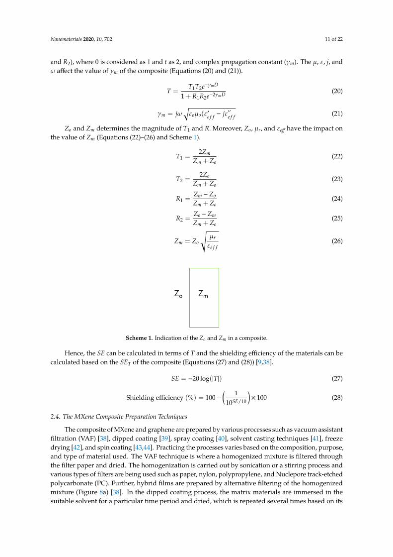
Zo and Zm determines the magnitude of T1 and R. Moreover, Zo, µr, and εeff have the impact onthe value of Zm (Equations (22)–(26) and Scheme 1).
T1 =2Zm
Zm + Zo(22)
T2 =2Zo
Zm + Zo(23)
R1 =Zm −Zo
Zm + Zo(24)
R2 =Zo −Zm
Zm + Zo(25)
Zm = Zo
õr
εe f f(26)
Nanomaterials 2020, 10, x FOR PEER REVIEW 12 of 23
The EMI shielding of the composites are complicated and the physiochemical properties of
constitutional composition of the composites which are significantly different from the homogeneous
shielding materials. The most imperative parameter for the theoretical calculation of the EMI
shielding is the effective relative permittivity εeff of the composite that can be calculated by using the
Maxwell Garnett formula. The εeff is determined by the relative permittivity of the matrix (εe), relative
permittivity of the fillers (εi), and f is the volume fraction of the filler. The εi is calculated by using the
imaginary part of the complex relative permittivity (ε ′and ε″), imaginary unit (j), б, ω , and εo
(Equations 18 and 19).
휀𝑒𝑓𝑓 = 휀𝑒 + 3𝑓휀𝑒
휀𝑖 − 휀𝑒
휀𝑖 + 2휀𝑒 − 𝑓(휀𝑖 − 휀𝑒) (18)
휀𝑖 = 휀′ − 𝑗휀′′ = 휀′ − 𝑗𝜎
𝜔휀𝑜 (19)
On the other hand, the EMI shielding can be expressed as how far a composite has transmitted
the EMR, which can be explained by using the transmission coefficient (T). The T is depending on the
transmission coefficient at the 0−t boundary (T1 and T2), reflection coefficient at the 0−t boundary (R1
and R2), where 0 is considered as 1 and t as 2, and complex propagation constant (γm). The μ, ε, j,
and ω affect the value of γm of the composite (Equations 20 and 21).
T = 𝑇1𝑇2𝑒−𝛾𝑚𝐷
1 + 𝑅1𝑅2𝑒−2𝛾𝑚𝐷 (20)
𝛾𝑚 = jω√휀𝑜𝜇𝑜(휀𝑒𝑓𝑓′ − 𝑗휀𝑒𝑓𝑓
′′ (21)
Scheme 1. Indication of the Zo and Zm in a composite.
Zo and Zm determines the magnitude of T1 and R. Moreover, Zo, μr, and εeff have the impact on
the value of Zm (Equations 22–26 and scheme 1).
𝑇1 =2𝑍𝑚
𝑍𝑚 + 𝑍𝑜 (22)
𝑇2 =2𝑍𝑜
𝑍𝑚 + 𝑍𝑜 (23)
𝑅1 =𝑍𝑚 − 𝑍𝑜
𝑍𝑚 + 𝑍𝑜 (24)
𝑅2 =𝑍𝑜 − 𝑍𝑚
𝑍𝑚 + 𝑍𝑜 (25)
𝑍𝑚 = 𝑍𝑜√𝜇𝑟
휀𝑒𝑓𝑓 (26)
Hence, the SE can be calculated in terms of T and the shielding efficiency of the materials can be
calculated based on the SET of the composite (Equations 27 and 28) [9,38].
Scheme 1. Indication of the Zo and Zm in a composite.
Hence, the SE can be calculated in terms of T and the shielding efficiency of the materials can becalculated based on the SET of the composite (Equations (27) and (28)) [9,38].
SE = −20 log(|T|) (27)
Shielding efficiency (%) = 100−( 1
10SE/10
)× 100 (28)
2.4. The MXene Composite Preparation Techniques
The composite of MXene and graphene are prepared by various processes such as vacuum assistantfiltration (VAF) [38], dipped coating [39], spray coating [40], solvent casting techniques [41], freezedrying [42], and spin coating [43,44]. Practicing the processes varies based on the composition, purpose,and type of material used. The VAF technique is where a homogenized mixture is filtered throughthe filter paper and dried. The homogenization is carried out by sonication or a stirring process andvarious types of filters are being used such as paper, nylon, polypropylene, and Nuclepore track-etchedpolycarbonate (PC). Further, hybrid films are prepared by alternative filtering of the homogenizedmixture (Figure 8a) [38]. In the dipped coating process, the matrix materials are immersed in thesuitable solvent for a particular time period and dried, which is repeated several times based on its
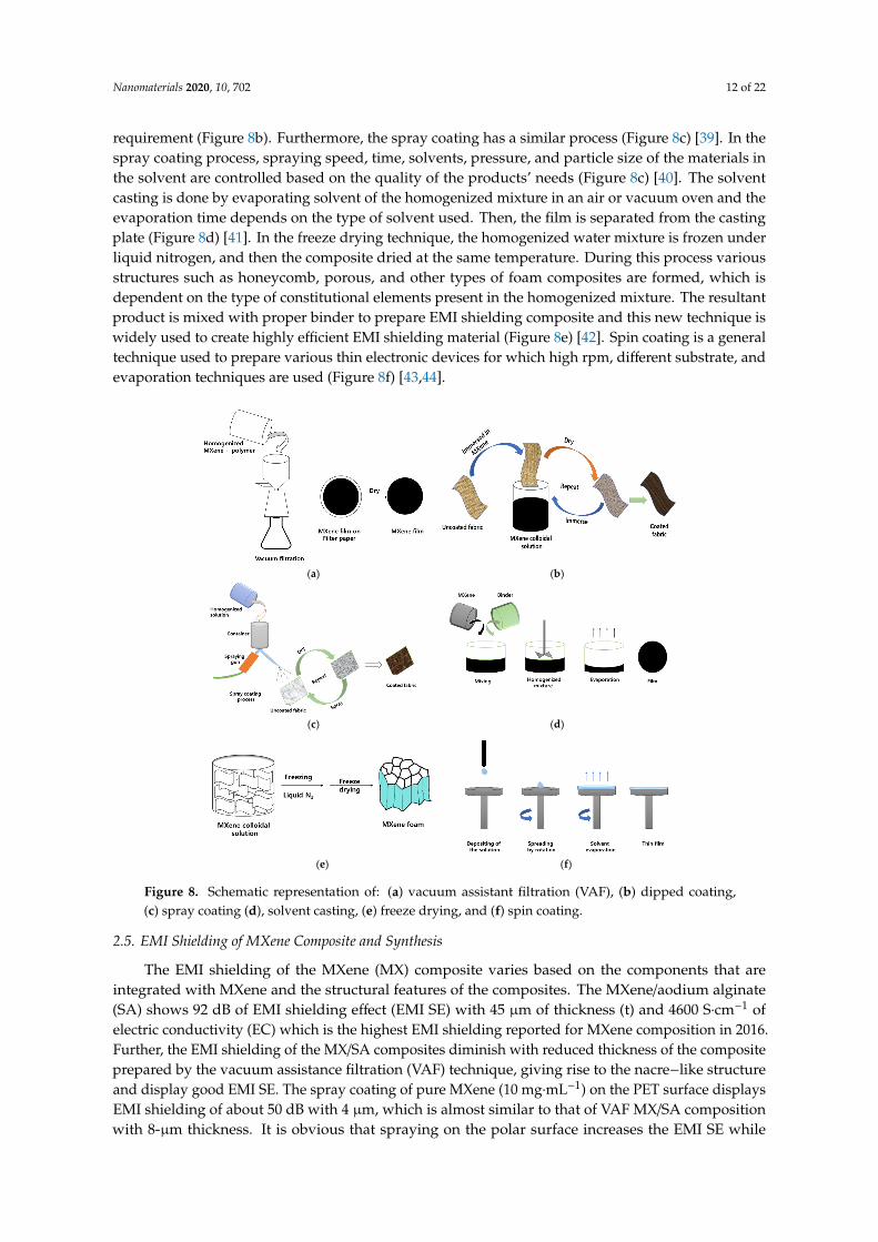
Nanomaterials 2020, 10, 702 12 of 22
requirement (Figure 8b). Furthermore, the spray coating has a similar process (Figure 8c) [39]. In thespray coating process, spraying speed, time, solvents, pressure, and particle size of the materials inthe solvent are controlled based on the quality of the products’ needs (Figure 8c) [40]. The solventcasting is done by evaporating solvent of the homogenized mixture in an air or vacuum oven and theevaporation time depends on the type of solvent used. Then, the film is separated from the castingplate (Figure 8d) [41]. In the freeze drying technique, the homogenized water mixture is frozen underliquid nitrogen, and then the composite dried at the same temperature. During this process variousstructures such as honeycomb, porous, and other types of foam composites are formed, which isdependent on the type of constitutional elements present in the homogenized mixture. The resultantproduct is mixed with proper binder to prepare EMI shielding composite and this new technique iswidely used to create highly efficient EMI shielding material (Figure 8e) [42]. Spin coating is a generaltechnique used to prepare various thin electronic devices for which high rpm, different substrate, andevaporation techniques are used (Figure 8f) [43,44].
Nanomaterials 2020, 10, x FOR PEER REVIEW 13 of 23
SE 20log |𝑇| (27) Shielding efficiency % 100 110 ⁄ 100 (28)
2.4. The MXene Composite Preparation Techniques.
The composite of MXene and graphene are prepared by various processes such as vacuum assistant filtration (VAF) [38], dipped coating [39], spray coating [40], solvent casting techniques [41], freeze drying [42], and spin coating [43,44]. Practicing the processes varies based on the composition, purpose, and type of material used. The VAF technique is where a homogenized mixture is filtered through the filter paper and dried. The homogenization is carried out by sonication or a stirring process and various types of filters are being used such as paper, nylon, polypropylene, and Nuclepore track-etched polycarbonate (PC). Further, hybrid films are prepared by alternative filtering of the homogenized mixture (Figure 8a) [38]. In the dipped coating process, the matrix materials are immersed in the suitable solvent for a particular time period and dried, which is repeated several times based on its requirement (Figure 8b). Furthermore, the spray coating has a similar process (Figure 8c) [39]. In the spray coating process, spraying speed, time, solvents, pressure, and particle size of the materials in the solvent are controlled based on the quality of the products’ needs (Figure 8c) [40]. The solvent casting is done by evaporating solvent of the homogenized mixture in an air or vacuum oven and the evaporation time depends on the type of solvent used. Then, the film is separated from the casting plate (Figure 8d) [41]. In the freeze drying technique, the homogenized water mixture is frozen under liquid nitrogen, and then the composite dried at the same temperature. During this process various structures such as honeycomb, porous, and other types of foam composites are formed, which is dependent on the type of constitutional elements present in the homogenized mixture. The resultant product is mixed with proper binder to prepare EMI shielding composite and this new technique is widely used to create highly efficient EMI shielding material (Figure 8e) [42]. Spin coating is a general technique used to prepare various thin electronic devices for which high rpm, different substrate, and evaporation techniques are used (Figure 8f) [43,44].
(a) (b)
(c) (d) Nanomaterials 2020, 10, x FOR PEER REVIEW 14 of 23
(e) (f)
Figure 8. Schematic representation of: (a) vacuum assistant filtration (VAF), (b) dipped coating, (c) spray coating (d), solvent casting, (e) freeze drying, and (f) spin coating.
2.5. EMI Shielding of MXene Composite and Synthesis
The EMI shielding of the MXene (MX) composite varies based on the components that are integrated with MXene and the structural features of the composites. The MXene/aodium alginate (SA) shows 92 dB of EMI shielding effect (EMI SE) with 45 μm of thickness (t) and 4600 S·cm−1 of electric conductivity (EC) which is the highest EMI shielding reported for MXene composition in 2016. Further, the EMI shielding of the MX/SA composites diminish with reduced thickness of the composite prepared by the vacuum assistance filtration (VAF) technique, giving rise to the nacre−like structure and display good EMI SE. The spray coating of pure MXene (10 mg·mL−1) on the PET surface displays EMI shielding of about 50 dB with 4 μm, which is almost similar to that of VAF MX/SA composition with 8-μm thickness. It is obvious that spraying on the polar surface increases the EMI SE while integration of the foreign element with MXene significantly reduces the EMI SE. Hence, the synthetic route influences the EMI shielding of the composite and the SA helps to arrange the MXene in a nacre array which significantly improves EMI SE of the shielding material (Figure 8 and Table 3) [45]. Hu et al. stated that the cellulose/MXene (M−filter) nanocomposite paper displays the 43 dB of EMI SE (seven cycle dipped coating) in both X and Ku band with 27.56 S·cm−1 of EC and thickness of 0.2 mm which is differ from the Coa et al. MX/cellulose composite performance. The MXene/cellulose composite exhibited EMI SE of 24 dB with SSE of 12 dB·cm3·g−1, 2647 dB.cm2·g−1, and 0.047 mm of thickness (Table 3) [39,46,47]. Hu et al. coated MXene with commercial filter paper (density of 0.49 g·cm−3) and then, utilized the polydimethylsiloxane (PDMS) for finishing purposes, denoted as PDMS−M−filter composite while Coa et al. used MXene/cellulose nanofiber (CNFs) derived from garlic husk and both practiced dipped coating and VAF, respectively. The nacre-inspired structure of MXene/CNFs, which is absent in dipped coating cellulose composite and present in VAF composite, is an inspired structural feature in the MXene/cellulose based composites. Further, the filler loading determines the EMI, EC, and tensile strength of the composite [39].
In addition, CNTs/MXene/cellulose nanofibrils composite paper prepared by facile alternating vacuum assisted filtration process give rise the 38.4 dB of EMI SE and corresponding EC and thickness are 25.066 S·cm−1 and 0.038 mm, respectively. The EMI SE of CNTs/MXene/cellulose is higher than that of MX/cellulose composite reported above. Thus, the introduction of the CNT enhances the EMI SE. A similar study reported by Raagulan et al. used MXene–carbon nanotube nanocomposites (MXCS) where carbon fabric is used instead of cellulose displayed 99.999% shielding ability. The EC of CNTs/MXene/cellulose nanofibrils composite is 2.12-times higher than that of MXCS. The difference of EMI shielding in both cases is due to the thickness, EC, and curved MXene multilayer structure [47,48]. Xin et al. described that intercalation of silver nanoparticle with MXene/cellulose composition enhanced EMI shielding and exhibited EMI SE of 50.7 dB with 46 μm thickness and 5.882 S·cm−1 of EC. In this case, the introduction of silver nanoparticle in cellulose and MXene composition formed a similar structure reported by Cao et al, and the silver ion causes self-reduction of MXene, which improved the EC, multilayer formation, dielectric constant, and conduction loss [49]. The fiber matrix helps to diffuse EMR and fillers and fibers attenuate the EMR. The study of Liu et al. showed that the aluminum ion reinforced MXene film exhibits the excellent EMI shielding of 80 dB with 2656 S·cm−1 of EC and 0.005 mm of thickness where aluminum ion plays
Figure 8. Schematic representation of: (a) vacuum assistant filtration (VAF), (b) dipped coating,(c) spray coating (d), solvent casting, (e) freeze drying, and (f) spin coating.
2.5. EMI Shielding of MXene Composite and Synthesis
The EMI shielding of the MXene (MX) composite varies based on the components that areintegrated with MXene and the structural features of the composites. The MXene/aodium alginate(SA) shows 92 dB of EMI shielding effect (EMI SE) with 45 µm of thickness (t) and 4600 S·cm−1 ofelectric conductivity (EC) which is the highest EMI shielding reported for MXene composition in 2016.Further, the EMI shielding of the MX/SA composites diminish with reduced thickness of the compositeprepared by the vacuum assistance filtration (VAF) technique, giving rise to the nacre−like structureand display good EMI SE. The spray coating of pure MXene (10 mg·mL−1) on the PET surface displaysEMI shielding of about 50 dB with 4 µm, which is almost similar to that of VAF MX/SA compositionwith 8-µm thickness. It is obvious that spraying on the polar surface increases the EMI SE while
Nanomaterials 2020, 10, 702 13 of 22
integration of the foreign element with MXene significantly reduces the EMI SE. Hence, the syntheticroute influences the EMI shielding of the composite and the SA helps to arrange the MXene in a nacrearray which significantly improves EMI SE of the shielding material (Figure 8 and Table 3) [45]. Hu et al.stated that the cellulose/MXene (M−filter) nanocomposite paper displays the 43 dB of EMI SE (sevencycle dipped coating) in both X and Ku band with 27.56 S·cm−1 of EC and thickness of 0.2 mm whichis differ from the Coa et al. MX/cellulose composite performance. The MXene/cellulose compositeexhibited EMI SE of 24 dB with SSE of 12 dB·cm3·g−1, 2647 dB.cm2
·g−1, and 0.047 mm of thickness(Table 3) [39,46,47]. Hu et al. coated MXene with commercial filter paper (density of 0.49 g·cm−3) andthen, utilized the polydimethylsiloxane (PDMS) for finishing purposes, denoted as PDMS−M−filtercomposite while Coa et al. used MXene/cellulose nanofiber (CNFs) derived from garlic husk and bothpracticed dipped coating and VAF, respectively. The nacre-inspired structure of MXene/CNFs, which isabsent in dipped coating cellulose composite and present in VAF composite, is an inspired structuralfeature in the MXene/cellulose based composites. Further, the filler loading determines the EMI, EC,and tensile strength of the composite [39].
In addition, CNTs/MXene/cellulose nanofibrils composite paper prepared by facile alternatingvacuum assisted filtration process give rise the 38.4 dB of EMI SE and corresponding EC and thicknessare 25.066 S·cm−1 and 0.038 mm, respectively. The EMI SE of CNTs/MXene/cellulose is higher thanthat of MX/cellulose composite reported above. Thus, the introduction of the CNT enhances theEMI SE. A similar study reported by Raagulan et al. used MXene–carbon nanotube nanocomposites(MXCS) where carbon fabric is used instead of cellulose displayed 99.999% shielding ability. The EC ofCNTs/MXene/cellulose nanofibrils composite is 2.12-times higher than that of MXCS. The difference ofEMI shielding in both cases is due to the thickness, EC, and curved MXene multilayer structure [47,48].Xin et al. described that intercalation of silver nanoparticle with MXene/cellulose composition enhancedEMI shielding and exhibited EMI SE of 50.7 dB with 46 µm thickness and 5.882 S·cm−1 of EC. In thiscase, the introduction of silver nanoparticle in cellulose and MXene composition formed a similarstructure reported by Cao et al. and the silver ion causes self-reduction of MXene, which improved theEC, multilayer formation, dielectric constant, and conduction loss [49]. The fiber matrix helps to diffuseEMR and fillers and fibers attenuate the EMR. The study of Liu et al. showed that the aluminum ionreinforced MXene film exhibits the excellent EMI shielding of 80 dB with 2656 S·cm−1 of EC and 0.005mm of thickness where aluminum ion plays a major role in EMI SE and tensile strength which is due tothe cross link formation between MXene and aluminum ion. Thus, aluminum ion has a greater tendencyto induce the EMI SE than sliver ion in the matrix of the composite [49,50]. Furthermore, conductivity ofthe aluminum reinforced MXene is lower than that of MX/SA composite which is due to the interlayerspace caused by the aluminum ion and higher than that of MXene/poly(3,4−ethylenedioxythiophene)polystyrene sulfonate (MX/PEDOT: PSS), MXCS, and d−Ti3C2Tx/CNFs reported (Table 3) [45,48–50].
The poly (vinyl alcohol)/MXene (PVA/MXene) multilayered composite reported by Jin et al.exhibits 44.4 dB (wt.%—19.5%) of EMI SE (SER—8.3 dB) with 0.027 mm of thickness and decrease withdecreasing MXene loading in the PVA matrix. MXene in a PVA matrix has a similar EC trend anddiminishes with less loading of MXene filler (Table 3) [51–53]. Further, the Xu et al. study shows thatthe PVA/MXene foam considerably minimized the EMI SE and exhibits 28 dB of EMI SE with a lowerSER (2 dB), which is due to the differences in EC and its porous nature. The SER above 3 dB is inducedby charge flow in the matrix. It is obvious that the EMI SE of the PVA/MXene composites are contingentnot only structural features, but also filler loading of the composite [53,54]. The honeycomb (HC)structure can be manufactured by using reduced graphene oxide (rGO)−MXene/epoxy compositionfor which the Al2O3 HC template is used. Initially, the rGO is adsorbed on the surface of the templateand then it is dissolved by using hydrochloric acid. Consequently, the HC graphene oxide is immersedinto the MXene/CTAB solution and freeze dried. The yielded HC−rGO/MXene is strengthened byepoxy polymer. The HC−rGO−MXene/epoxy composition displays EMI SE of 55 dB with 3.871 S·cm−1
of EC and 0.5 mm of thickness [55,56]. A similar study is performed by Bian et al. who preparedMXene aerogel without a template and its corresponding EMI SE of 75 dB and SER is about 1 dB [57].
Nanomaterials 2020, 10, 702 14 of 22
The EC of HC−GO−MXene/epoxy composite is lower than that of MXene aerogel which is due tothe interconnection between MXene and epoxy polymer comparatively lessened the EMI SE andEC. The epoxy polymer not only minimized the electron flow among MXene and graphene but alsoimproved the tensile strength of the composite and flexibility [56,57]. Zhou et al. described that theMXene/calcium alginate aerogel ((MX/CA (t = 26 µm)) exhibits 54.43 dB of EMI SE which is higher thanthat of the MX/SA composite synthesized in the same condition (t = 14 µm) (Table 3) [58]. Although,the 8 µm MX/SA reported by Shahzad et al. exhibited 57 dB of EMI SE which is assumed as the qualityof the exfoliated MXene synthesized and fabrication condition used (Table 3) [46,58]. Further, thethickness or inter space of the composite is increased by types of interacting ion or organic substancesused which also affect the EMI SE parameters. The thickness of the MX/CA is higher than the MX/SAwhich is caused by calcium alginate and aerogel structure of MX/CA diminished the EC and increasedthe corresponding SSE/t of the composite (Table 3) [58].
The interposing of the rGO into MXene formed, MX/rGO aerogel shows 56.4 dB of EMI SE whichis almost similar to the HC−MX−rGO/epoxy composite, thus, the HC structure is an effective featurewith the lowest thickness and filling load [56,59]. Scientists recently focusses on the 3D aerogel whichseems to be a more effective EMI absorbent than the planar composite. The 3D Ti3C2Tx/SA (95%)hybrid aerogel coated by electrically conductive polydimethylsiloxane−coated (PDMS) displays EMISE of 70.5 dB and corresponding EC is 22.11 S·cm−1. In addition, the higher amount of SA reducesthe EMI SE and EC. Further, SEA and SET are almost similar where SER seems null is an evidencethat the aerogel structure greatly improved absorption and the direct interconnection of MXene is acrucial parameter for EMI SE and SEA [42]. Further, introduction of carbon into the MXene framework(MXene/carbon foam (MCF)) showed less EMI SE of 8 dB and addition of epoxy polymer followed byannealing of MCF reached up to EMI SE of 46 dB with 1.84 S·cm−1 of EC (2 cm of thickness). In thisstudy, the resorcinol−formaldehyde sol−gel mixture is used as a precursor for carbon form, created byan annealing process, nonetheless, Song et al.’s epoxy composite consisted of rGO as a carbon formgave rise to higher EMI SE (55 dB) [56,60]. Hence, the filler with good electric conductivity and propergeometry improved EMI SE [60]. Furthermore, Wang, et al. reported that the annealed MXene/EpoxyNano composites (wt.% 15) with 41 dB of EMI SE, 2 cm of thickness and 1.05 S·cm−1. From thesestudies, the annealing of composite internally created a carbon form from polymer that significantlychanged EC and EMI SE. The direct annealing of pure MXene reduce the EMI shielding and due to thecuring ability epoxy in MXene/Epoxy composite matrix enhances EMI SE [42,60].
Mixing of silver nanowire with MXene with cellulose pressured-extrusion method blocked 99.99%of incoming EMR, which is lower than that of pure MXene, and silver nanowire improved theelectron flow path between 1D and 2D filler (Table 3) [45,61]. The corresponding composite assembledlike brick-and-mortar like arrangement with internal pores which provide reflection and scatteringinterfaces that improve EMI SE [61]. Further, the heat treated monolayer MXene with 4.14 × 10⁻⁵ mm ofthickness shows EMI SE of 17.13 dB and corresponding SSE and SSE/t are 7.17 dB·cm3
·g−1 and 1.73× 10⁶dB·cm2·g−1, respectively. The corresponding composite (without heat process) with the same thicknessdisplays EMI SE, SSE, and SSE/t of 13.56 dB, 5.67 dB·cm3
·g−1, and 1.37 × 10⁶ dB·cm3·g−1, respectively.
It is apparent that the annealing at 600 C improve EMI SE and other parameters significantly [43].Wan et al. produced MXene/PEDOT: PSS composite with 6 µm of thickness gave rise to 40.5 dB ofEMI SE while the same composition reported by Liu et al. showed 42.1 dB of EMI SE with 11 µmof thickness from which the preparation method plays a major role in determining the EMI SE. Theremoval of PSS from the matrix increase EMI shielding with 6 µm of thickness which is the mainreason for Wan et al.’s results [38,62,63]. The SEA mostly depends on the dielectric properties of theEMI shielding composite. Han et al. alter the surface of the MXene by annealing at 800 C under theinert environment and prepare the MXene/wax composite (1 mm) display show EMI SE of 76.1 dBwith 67.3 dB of SEA and corresponding composite exhibit −48.4 dB of minimum reflection coefficientwhich is due to the formation of the titanium oxide on the surface of the MXene [64,65].
Nanomaterials 2020, 10, 702 15 of 22
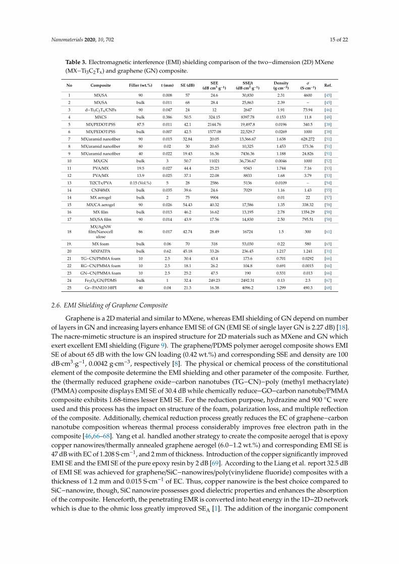
Table 3. Electromagnetic interference (EMI) shielding comparison of the two−dimension (2D) MXene(MX−Ti3C2Tx) and graphene (GN) composite.
No Composite Filler (wt.%) t (mm) SE (dB) SEE(dB cm3
·g−1)SSE/t
(dB·cm2·g−1)
Density(g·cm−3)
σ(S·cm−1)
Ref.
1 MX/SA 90 0.008 57 24.6 30,830 2.31 4600 [45]
2 MX/SA bulk 0.011 68 28.4 25,863 2.39 − [45]
3 d−Ti3C2Tx/CNFs 90 0.047 24 12 2647 1.91 73.94 [46]
4 MXCS bulk 0.386 50.5 324.15 8397.78 0.153 11.8 [48]
5 MX/PEDOT:PSS 87.5 0.011 42.1 2144.76 19,497.8 0.0196 340.5 [38]
6 MX/PEDOT:PSS bulk 0.007 42.5 1577.08 22,529.7 0.0269 1000 [38]
7 MX/aramid nanofiber 90 0.015 32.84 20.05 13,366.67 1.638 628.272 [51]
8 MX/aramid nanofiber 80 0.02 30 20.65 10,325 1.453 173.36 [51]
9 MX/aramid nanofiber 40 0.022 19.43 16.36 7436.36 1.188 24.826 [51]
10 MX/GN bulk 3 50.7 11021 36,736.67 0.0046 1000 [52]
11 PVA/MX 19.5 0.027 44.4 25.23 9343 1.744 7.16 [53]
12 PVA/MX 13.9 0.025 37.1 22.08 8833 1.68 3.79 [53]
13 Ti2CTx/PVA 0.15 (Vol.%) 5 28 2586 5136 0.0109 − [54]
14 CNF@MX bulk 0.035 39.6 24.6 7029 1.16 1.43 [55]
14 MX aerogel bulk 2 75 9904 0.01 22 [57]
15 MX/CA aerogel 90 0.026 54.43 40.32 17,586 1.35 338.32 [58]
16 MX film bulk 0.013 46.2 16.62 13,195 2.78 1354.29 [58]
17 MX/SA film 90 0.014 43.9 17.56 14,830 2.50 795.51 [58]
18MX/AgNW
film/Nanocellulose
86 0.017 42.74 28.49 16724 1.5 300 [61]
19. MX foam bulk 0.06 70 318 53,030 0.22 580 [65]
20 MXPATPA bulk 0.62 45.18 33.26 236.45 1.217 1.241 [31]
21 TG−CN/PMMA foam 10 2.5 30.4 43.4 173.6 0.701 0.0292 [66]
22 RG−CN/PMMA foam 10 2.5 18.1 26.2 104.8 0.691 0.0015 [66]
23 GN−CN/PMMA foam 10 2.5 25.2 47.5 190 0.531 0.013 [66]
24 Fe3O4/GN/PDMS bulk 1 32.4 249.23 2492.31 0.13 2.5 [67]
25 Gr−PANI10:1@PI 40 0.04 21.3 16.38 4096.2 1.299 490.3 [68]
2.6. EMI Shielding of Graphene Composite
Graphene is a 2D material and similar to MXene, whereas EMI shielding of GN depend on numberof layers in GN and increasing layers enhance EMI SE of GN (EMI SE of single layer GN is 2.27 dB) [18].The nacre-mimetic structure is an inspired structure for 2D materials such as MXene and GN whichexert excellent EMI shielding (Figure 9). The graphene/PDMS polymer aerogel composite shows EMISE of about 65 dB with the low GN loading (0.42 wt.%) and corresponding SSE and density are 100dB·cm3
·g−1, 0.0042 g·cm−3, respectively [8]. The physical or chemical process of the constitutionalelement of the composite determine the EMI shielding and other parameter of the composite. Further,the (thermally reduced graphene oxide−carbon nanotubes (TG−CN)−poly (methyl methacrylate)(PMMA) composite displays EMI SE of 30.4 dB while chemically reduce−GO−carbon nanotube/PMMAcomposite exhibits 1.68-times lesser EMI SE. For the reduction purpose, hydrazine and 900 C wereused and this process has the impact on structure of the foam, polarization loss, and multiple reflectionof the composite. Additionally, chemical reduction process greatly reduces the EC of graphene−carbonnanotube composition whereas thermal process considerably improves free electron path in thecomposite [46,66–68]. Yang et al. handled another strategy to create the composite aerogel that is epoxycopper nanowires/thermally annealed graphene aerogel (6.0−1.2 wt.%) and corresponding EMI SE is47 dB with EC of 1.208 S·cm−1, and 2 mm of thickness. Introduction of the copper significantly improvedEMI SE and the EMI SE of the pure epoxy resin by 2 dB [69]. According to the Liang et al. report 32.5 dBof EMI SE was achieved for graphene/SiC−nanowires/poly(vinylidene fluoride) composites with athickness of 1.2 mm and 0.015 S·cm−1 of EC. Thus, copper nanowire is the best choice compared toSiC−nanowire, though, SiC nanowire possesses good dielectric properties and enhances the absorptionof the composite. Henceforth, the penetrating EMR is converted into heat energy in the 1D−2D networkwhich is due to the ohmic loss greatly improved SEA [1]. The addition of the inorganic component
Nanomaterials 2020, 10, 702 16 of 22
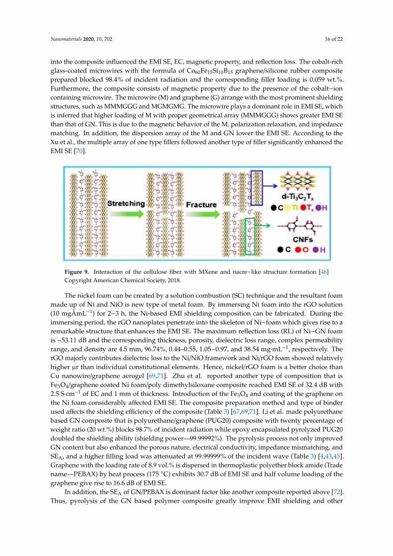
into the composite influenced the EMI SE, EC, magnetic property, and reflection loss. The cobalt-richglass-coated microwires with the formula of Co60Fe15Si10B15 graphene/silicone rubber compositeprepared blocked 98.4% of incident radiation and the corresponding filler loading is 0.059 wt.%.Furthermore, the composite consists of magnetic property due to the presence of the cobalt−ioncontaining microwire. The microwire (M) and graphene (G) arrange with the most prominent shieldingstructures, such as MMMGGG and MGMGMG. The microwire plays a dominant role in EMI SE, whichis inferred that higher loading of M with proper geometrical array (MMMGGG) shows greater EMI SEthan that of GN. This is due to the magnetic behavior of the M, polarization relaxation, and impedancematching. In addition, the dispersion array of the M and GN lower the EMI SE. According to theXu et al., the multiple array of one type fillers followed another type of filler significantly enhanced theEMI SE [70].
Nanomaterials 2020, 10, x FOR PEER REVIEW 18 of 23
coated microwires with the formula of Co60Fe15Si10B15 graphene/silicone rubber composite prepared
blocked 98.4% of incident radiation and the corresponding filler loading is 0.059 wt.%. Furthermore,
the composite consists of magnetic property due to the presence of the cobalt−ion containing
microwire. The microwire (M) and graphene (G) arrange with the most prominent shielding
structures, such as MMMGGG and MGMGMG. The microwire plays a dominant role in EMI SE,
which is inferred that higher loading of M with proper geometrical array (MMMGGG) shows greater
EMI SE than that of GN. This is due to the magnetic behavior of the M, polarization relaxation, and
impedance matching. In addition, the dispersion array of the M and GN lower the EMI SE. According
to the Xu et al., the multiple array of one type fillers followed another type of filler significantly
enhanced the EMI SE [70].
Figure 9. Interaction of the cellulose fiber with MXene and nacre−like structure formation [46]
Copyright American Chemical Society, 2018.
The nickel foam can be created by a solution combustion (SC) technique and the resultant foam
made up of Ni and NiO is new type of metal foam. By immersing Ni foam into the rGO solution (10
mgÅ mL−1) for 2−3 h, the Ni-based EMI shielding composition can be fabricated. During the
immersing period, the rGO nanoplates penetrate into the skeleton of Ni−foam which gives rise to a
remarkable structure that enhances the EMI SE. The maximum reflection loss (RL) of Ni−GN foam is
−53.11 dB and the corresponding thickness, porosity, dielectric loss range, complex permeability
range, and density are 4.5 mm, 96.74%, 0.44–0.55, 1.05−0.97, and 38.54 mg·mL−1, respectively. The rGO
majorly contributes dielectric loss to the Ni/NiO framework and Ni/rGO foam showed relatively
higher μr than individual constitutional elements. Hence, nickel/rGO foam is a better choice than Cu
nanowire/graphene aerogel [69,71]. Zhu et al. reported another type of composition that is
Fe3O4/graphene coated Ni foam/poly dimethylsiloxane composite reached EMI SE of 32.4 dB with 2.5
S·cm−1 of EC and 1 mm of thickness. Introduction of the Fe3O4 and coating of the graphene on the Ni
foam considerably affected EMI SE. The composite preparation method and type of binder used
affects the shielding efficiency of the composite (Table 3) [67,69,71]. Li et al. made polyurethane based
GN composite that is polyurethane/graphene (PUG20) composite with twenty percentage of weight
ratio (20 wt.%) blocks 98.7% of incident radiation while epoxy encapsulated pyrolyzed PUG20
doubled the shielding ability (shielding power—99.99992%). The pyrolysis process not only
improved GN content but also enhanced the porous nature, electrical conductivity, impedance
mismatching, and SEA, and a higher filling load was attenuated at 99.99999% of the incident wave
(Table 3) [4,43,45]. Graphene with the loading rate of 8.9 vol.% is dispersed in thermoplastic polyether
block amide (Trade name—PEBAX) by heat process (175 ) exhibits 30.7 dB of EMI SE and half
volume loading of the graphene give rise to 16.6 dB of EMI SE.
In addition, the SEA of GN/PEBAX is dominant factor like another composite reported above
[72]. Thus, pyrolysis of the GN based polymer composite greatly improve EMI shielding and other
parameters such as EC, dielectric property, porous structure, permeability, etc. The CNTs
co−decorated porous carbon/graphene/PDMS foam generate 48 dB of shielding ability and
corresponding SSE is 347.8 dB·g−1·cm3. The composite consists multilayer of components those design
is better than that of the Zhu et al. study. The Ni foam is coated by CNT (GF) by the CVD method
Figure 9. Interaction of the cellulose fiber with MXene and nacre−like structure formation [46]Copyright American Chemical Society, 2018.
The nickel foam can be created by a solution combustion (SC) technique and the resultant foammade up of Ni and NiO is new type of metal foam. By immersing Ni foam into the rGO solution(10 mgÅmL−1) for 2−3 h, the Ni-based EMI shielding composition can be fabricated. During theimmersing period, the rGO nanoplates penetrate into the skeleton of Ni−foam which gives rise to aremarkable structure that enhances the EMI SE. The maximum reflection loss (RL) of Ni−GN foamis −53.11 dB and the corresponding thickness, porosity, dielectric loss range, complex permeabilityrange, and density are 4.5 mm, 96.74%, 0.44–0.55, 1.05−0.97, and 38.54 mg·mL−1, respectively. TherGO majorly contributes dielectric loss to the Ni/NiO framework and Ni/rGO foam showed relativelyhigher µr than individual constitutional elements. Hence, nickel/rGO foam is a better choice thanCu nanowire/graphene aerogel [69,71]. Zhu et al. reported another type of composition that isFe3O4/graphene coated Ni foam/poly dimethylsiloxane composite reached EMI SE of 32.4 dB with2.5 S·cm−1 of EC and 1 mm of thickness. Introduction of the Fe3O4 and coating of the graphene onthe Ni foam considerably affected EMI SE. The composite preparation method and type of binderused affects the shielding efficiency of the composite (Table 3) [67,69,71]. Li et al. made polyurethanebased GN composite that is polyurethane/graphene (PUG20) composite with twenty percentage ofweight ratio (20 wt.%) blocks 98.7% of incident radiation while epoxy encapsulated pyrolyzed PUG20doubled the shielding ability (shielding power—99.99992%). The pyrolysis process not only improvedGN content but also enhanced the porous nature, electrical conductivity, impedance mismatching, andSEA, and a higher filling load was attenuated at 99.99999% of the incident wave (Table 3) [4,43,45].Graphene with the loading rate of 8.9 vol.% is dispersed in thermoplastic polyether block amide (Tradename—PEBAX) by heat process (175 C) exhibits 30.7 dB of EMI SE and half volume loading of thegraphene give rise to 16.6 dB of EMI SE.
In addition, the SEA of GN/PEBAX is dominant factor like another composite reported above [72].Thus, pyrolysis of the GN based polymer composite greatly improve EMI shielding and other
Nanomaterials 2020, 10, 702 17 of 22
parameters such as EC, dielectric property, porous structure, permeability, etc. The CNTs co−decoratedporous carbon/graphene/PDMS foam generate 48 dB of shielding ability and corresponding SSEis 347.8 dB·g−1
·cm3. The composite consists multilayer of components those design is better thanthat of the Zhu et al. study. The Ni foam is coated by CNT (GF) by the CVD method and Fe−Znco−precipitated on hydrothermal method (FCC−GF) which is dispersed in the PDMS matrix [G11].The Zhu et al. study just used an electrostatic assemble of nanomaterials on the porous structurethat has less effect on EMI SE and CVD, or a hydro thermal process improved porous geometry andminimized the defect of fillers [67,73].
The many studies use PDMS as a binder to make GN-based EMI shielding materials. The 3Dgraphene/carbon nanotubes/polydimethylsiloxane composites (GC) was prepared by using freezedrying followed by annealing at a high temperature (2800 C) and this is similar to the Song et al.study where they used the HC template to create the aerogel [58,74]. GC with 95.8% of porosity,0.013 g·cm−3 of density, 2.4 mm of thickness, and 92.78 (vol.%) loading rate annealed at 1400 C gaverise to 54.43 dB of highest EMI SE and the corresponding EC is 0.2012 S·cm−1. The higher annealingtemperature (2800 C) destroys EMI shielding of the composite, whereas the higher temperature repairsthe defects by removing functional groups, reduced polarization loss, lessens the amorphous nature(higher amorphous nature at 1400 C) and enhances the ohmic loss. Further, the introduction of theCNT prevents the agglomeration of GN and enhance the electric channels in the 3D network [58,74].Cheng et al. prepared graphene−polyaniline (PANI)@polyimide composite with a ratio of 10:1 (GN:PANI) shows 21.3 dB (t − 0.04 mm) with 490.3 S·cm−1 of EC while GN/PANI, Ni decorated GN/PANIand Ag decorated GN/PANI (5 wt.%) show EMI SE of 24.85, 29.33, and 24.93 dB, respectively. Therefore,metal nanoparticle decoration with GN in PANI matrix improved EMI SE compared to the GN/PANIin polyimide matrix [68,75,76].
The electrical conductivity of the pure materials is high compared to the composite made fromcorresponding pure materials. Further, MXene based composition showed excellent EC compared tothe GN. This is because of the functional group present in the MXene gave rise to a better arrangementin the polymer matrix which promoted a good electron flow path. Due to this, MXene is one of themost attractive materials in the modern electronic world. The SSE and SSE/t is depend on the densityand thickness of the composite. Further, proper geometrical arrangement of the fillers is a crucial factorfor better EMI shielding.
3. Conclusions
In this review, we have highlighted recent progress in EMI shielding of MXene and graphenecomposite with different fabrication technique. The global requirement is a lightweight, flexible,cost−effective, and thinner EMI shielding material and EMI shielding over 20 dB, which is the basicrequirement for the EMI shielding application in electronic devices. The graphene is synthesized byvarious methods in which radiative and chemical vapor deposition gives rise to good quality grapheneand utilization of other methods is dependent on the types of applications. MXene synthesis alsoadapts various techniques and the lithium fluoride/hydrochloric acid etching is the most desirableetching method. The 2D MXene and graphene play a major role in creating different structures,especially aerogel. The freezing and freeze-drying process is used to prepare different geometriccomposite with excellent EMI shielding is a new approach. Further, the pyrolysis and hydrothermalprocess are important techniques used to achieve higher EMI shielding of the aerogel hybrid structure.The pyrolysis process of MXene created with surface titanium oxide, induces the EMI shielding whileannealing of the MXene/polymer composite forms an internal conductive carbon network is anotherapproach for excellent EMI shielding. The high temperature pyrolysis process of MXene or graphenepolymer composite destroyed the EMI shielding function. The EMI shielding of graphene can beimproved further by doping, decoration, oxidation, reduction, encapsulation, type of polymer, andprocessing technique. Thus, the proper geometrical arrangement of the fillers is a crucial factor for betterEMI shielding and can be tuned by changing thickness, porosity, dielectric loss range, and complex
Nanomaterials 2020, 10, 702 18 of 22
permeability. The addition of inorganic nano composition like nanowire, ions, and nanoparticle furtherenhances EMI shielding and are being used to make the most powerful EMI shielding composites.The polymer/filler composites are explored to fulfil recent demand in EMI shielding in electronicdevices. We hope, we have provided the fundamental understanding of MXene, graphene, and itscorresponding composites to achieve a modern electronic goal in the near future.
Author Contributions: K.Y.C. designed the project; B.M.K. and K.R. wrote the manuscript. All authors have readand agreed to the published version of the manuscript.
Funding: This research received no external funding.
Acknowledgments: This study was supported by Wonkwang University 2019.
Conflicts of Interest: The authors declare no conflict of interest.
References
1. Liang, C.; Hamidinejad, M.; Ma, L.; Wang, Z.; Park, C.B. Lightweight and flexiblegraphene/SiC-nanowires/poly (vinylidene fluoride) composites for electromagnetic interference shieldingand thermal management. Carbon 2020, 156, 58–66. [CrossRef]
2. Xing, D.; Lu, L.; Xie, Y.; Tang, Y.; Teh, K.S. Highly flexible and ultra-thin carbon-fabric/Ag/waterbornepolyurethane film for ultra-efficient EMI shielding. Mater. Des. 2020, 185, 108227. [CrossRef]
3. Sheng, A.; Ren, W.; Yang, Y.; Yan, D.X.; Duan, H.; Zhao, G.; Liu, Y.; Li, Z.M. Multilayer WPUconductive composites with controllable electro-magnetic gradient for absorption-dominated electromagneticinterference shielding. Compos. Part A: Appl. Sci. Manuf. 2020, 129, 105692. [CrossRef]
4. Li, Y.; Liu, J.; Wang, S.; Zhang, L.; Shen, B. Self-templating graphene network composites by flamecarbonization for excellent electromagnetic interference shielding. Compos. Part B: Eng. 2020, 182, 107615.[CrossRef]
5. Zhao, B.; Zeng, S.; Li, X.; Guo, X.; Bai, Z.; Fan, B.; Zhang, R. Flexible PVDF/carbon materials/Ni compositefilms maintaining strong electromagnetic wave shielding under cyclic microwave irradiation. J. Mater. Chem.C 2020, 8, 500–509.
6. Shukla, V. Role of spin disorder in magnetic and EMI shielding properties of Fe3O4/C/PPy core/shellcomposites. J. Mater. Sci. 2020, 55, 2826–2835. [CrossRef]
7. Li, T.T.; Wang, Y.; Peng, H.K.; Zhang, X.; Shiu, B.C.; Lin, J.H.; Lou, C.W. Lightweight, flexible andsuperhydrophobic composite nanofiber films inspired by nacre for highly electromagnetic interferenceshielding. Compos. Part A: Appl. Sci. Manuf. 2020, 128, 105685. [CrossRef]
8. Gao, W.; Zhao, N.; Yu, T.; Xi, J.; Mao, A.; Yuan, M.; Bai, H.; Gao, C. High-efficiency electromagnetic interferenceshielding realized in nacre-mimetic graphene/polymer composite with extremely low graphene loading.Carbon 2020, 157, 570–577. [CrossRef]
9. Langguth, W. Earthing & EMC Fundamentals of Electromagnetic Compatibility (EMC). Power Qual. Appl.Guide Copp. Dev. Assoc. 2006, 6, 1–16.
10. Wang, Y.; Wang, H.; Ye, J.; Shi, L.; Feng, X. Magnetic CoFe alloy@ C nanocomposites derived from ZnCo-MOFfor electromagnetic wave absorption. Chem. Eng. J. 2020, 383, 123096. [CrossRef]
11. Singh, A.K.; Yadav, A.N.; Srivastava, A.; Haldar, K.K.; Tomar, M.; Alaferdov, A.V.; Moshkalev, S.A.; Gupta, V.;Singh, K. CdSe/V2O5 core/shell quantum dots decorated reduced graphene oxide nanocomposite forhigh-performance electromagnetic interference shielding application. Nanotechnology 2019, 30, 505704.[CrossRef] [PubMed]
12. Hawkins, S.A.; Yao, H.; Wang, H.; Sue, H.J. Tensile properties and electrical conductivity of epoxy compositethin films containing zinc oxide quantum dots and multi-walled carbon nanotubes. Carbon 2017, 115, 18–27.[CrossRef]
13. El-Shamy, A.G. Novel conducting PVA/Carbon quantum dots (CQDs) nanocomposite for highanti-electromagnetic wave performance. J. Alloys Compd. 2019, 810, 151940. [CrossRef]
14. Ge, C.; Zou, J.; Yan, M.; Bi, H. C-dots induced microwave absorption enhancement of PANI/ferrocene/C-dots.Mater. Lett. 2014, 137, 41–44. [CrossRef]
15. Lakshmi, N.V.; Tambe, P. EMI shielding effectiveness of graphene decorated with graphene quantum dotsand silver nanoparticles reinforced PVDF nanocomposites. Compos. Interfaces 2017, 24, 861–882. [CrossRef]
Nanomaterials 2020, 10, 702 19 of 22
16. Ji, B.; Giovanelli, E.; Habert, B.; Spinicelli, P.; Nasilowski, M.; Xu, X.; Lequeux, N.; Hugonin, J.P.; Marquier, F.;Greffet, J.J.; et al. Non-blinking quantum dot with a plasmonic nanoshell resonator. Nat. Nanotechnol. 2015,10, 170. [CrossRef] [PubMed]
17. Wang, Y.; Wang, W.; Qi, Q.; Xu, N.; Yu, D. Layer-by-layer assembly of PDMS-coated nickel ferrite/multiwalledcarbon nanotubes/cotton fabrics for robust and durable electromagnetic interference shielding. Cellulose2020, 27, 2829–2845. [CrossRef]
18. Kumar, P. Ultrathin 2D Nanomaterials for Electromagnetic Interference Shielding. Adv. Mater. Interfaces2019, 6, 1901454. [CrossRef]
19. Sangwan, V.K.; Hersam, M.C. Electronic transport in two-dimensional materials. Annu. Rev. Phys. Chem.2018, 69, 299–325. [CrossRef]
20. Le, M.Q.; Nguyen, D.T. The role of defects in the tensile properties of silicene. Appl. Phys. A 2015, 118,1437–1445. [CrossRef]
21. Fan, X.; Ma, Y.; Dang, X.; Cai, Y. Synthesis and Electromagnetic Interference Shielding Performance ofTi3SiC2-Based Ceramics Fabricated by Liquid Silicon Infiltration. Materials 2020, 13, 328. [CrossRef][PubMed]
22. Guan, H.; Chung, D.D.L. Radio-wave electrical conductivity and absorption-dominant interaction withradio wave of exfoliated-graphite-based flexible graphite, with relevance to electromagnetic shielding andantennas. Carbon 2020, 157, 549–562. [CrossRef]
23. Shams, S.S.; Zhang, R.; Zhu, J. Graphene synthesis: A Review. Mater. Sci.-Pol. 2015, 33, 566–578. [CrossRef]24. Lee, H.C.; Liu, W.W.; Chai, S.P.; Mohamed, A.R.; Aziz, A.; Khe, C.S.; Hidayah, N.M.; Hashim, U. Review of
the synthesis, transfer, characterization and growth mechanisms of single and multilayer graphene. RSCAdv. 2017, 7, 15644–15693. [CrossRef]
25. Persichetti, L.; De Seta, M.; Scaparro, A.M.; Miseikis, V.; Notargiacomo, A.; Ruocco, A.; Sgarlata, A.;Fanfoni, M.; Fabbri, F.; Coletti, C.; et al. Driving with temperature the synthesis of graphene on Ge (110).Appl. Surf. Sci. 2020, 499, 143923. [CrossRef]
26. Kumar, K.T.; Reddy, M.J.K.; Sundari, G.S.; Raghu, S.; Kalaivani, R.A.; Ryu, S.H.; Shanmugharaj, A.M. Synthesisof graphene-siloxene nanosheet based layered composite materials by tuning its interface chemistry: Anefficient anode with overwhelming electrochemical performances for lithium-ion batteries. J. Power Sources2020, 450, 227618. [CrossRef]
27. Yoon, K.Y.; Dong, G. Liquid-phase bottom-up synthesis of graphene nanoribbons. Mater. Chem. Front. 2020,4, 29–45. [CrossRef]
28. Wong, K.L.; Chuan, M.W.; Hamzah, A.; Rusli, S.; Alias, N.E.; Sultan, S.M.; Lim, C.S.; Tan, M.L.P. Electronicproperties of graphene nanoribbons with line-edge roughness doped with nitrogen and boron. Phys. E:Low-Syst. Nanostruct. 2020, 117, 113841. [CrossRef]
29. Yang, G.; Li, L.; Lee, W.B.; Ng, M.C. Structure of graphene and its disorders: A review. Sci. Technol. Adv.Mater. 2018, 19, 613–648. [CrossRef]
30. Wallace, P.R. The band theory of graphite. Phys. Rev. 1947, 71, 622. [CrossRef]31. Raagulan, K.; Braveenth, R.; Kim, B.M.; Lim, K.J.; Lee, S.B.; Kim, M.; Chai, K.Y. An effective utilization
of MXene and its effect on electromagnetic interference shielding: Flexible, free-standing and thermallyconductive composite from MXene-AT-poly (p-aminophenol)–polyaniline co-polymer. RSC Adv. 2020, 10,1613–1633. [CrossRef]
32. Yury, G.; Anasori, B. The Rise of MXenes. ACS Nano 2019, 13, 8491–8494.33. Alhabeb, M.; Maleski, K.; Anasori, B.; Lelyukh, P.; Clark, L.; Sin, S.; Gogotsi, Y. Guidelines for synthesis
and processing of two-dimensional titanium carbide (Ti3C2T ×MXene). Chem. Mater. 2017, 29, 7633–7644.[CrossRef]
34. Shukla, V. Review of electromagnetic interference shielding materials fabricated by iron ingredients. NanoscaleAdv. 2019, 1, 1640–1671. [CrossRef]
35. Nasouri, K.; Shoushtari, A.M.; Mojtahedi, M.R.M. Theoretical and experimental studies on EMI shieldingmechanisms of multi-walled carbon nanotubes reinforced high performance composite nanofibers. J. Polym.Res. 2016, 23, 71. [CrossRef]
36. Bi, S.; Zhang, L.; Mu, C.; Liu, M.; Hu, X. Electromagnetic interference shielding properties and mechanismsof chemically reduced graphene aerogels. Appl. Surf. Sci. 2017, 412, 529–536. [CrossRef]
Nanomaterials 2020, 10, 702 20 of 22
37. Drakakis, E.; Kymakis, E.; Tzagkarakis, G.; Louloudakis, D.; Katharakis, M.; Kenanakis, G.; Suchea, M.;Tudose, V.; Koudoumas, E. A study of the electromagnetic shielding mechanisms in the GHz frequencyrange of graphene based composite layers. Appl. Surf. Sci. 2017, 398, 15–18. [CrossRef]
38. Liu, R.; Miao, M.; Li, Y.; Zhang, J.; Cao, S.; Feng, X. Ultrathin Biomimetic Polymeric Ti3C2T × MXeneComposite Films for Electromagnetic Interference Shielding. ACS Appl. Mater. Interfaces 2018, 10, 44787–44795.[CrossRef]
39. Hu, D.; Huang, X.; Li, S.; Jiang, P. Flexible and durable cellulose/MXene nanocomposite paper for efficientelectromagnetic interference shielding. Compos. Sci. Technol. 2020, 188, 107995. [CrossRef]
40. Hantanasirisakul, K.; Zhao, M.Q.; Urbankowski, P.; Halim, J.; Anasori, B.; Kota, S.; Ren, C.E.; Barsoum, M.W.;Gogotsi, Y. Fabrication of Ti3C2Tx MXene transparent thin films with tunable optoelectronic properties. Adv.Electron. Mater. 2016, 2, 1600050. [CrossRef]
41. Naguib, M.; Saito, T.; Lai, S.; Rager, M.S.; Aytug, T.; Paranthaman, M.P.; Zhao, M.Q.; Gogotsi, Y. Ti3C2Tx(MXene)–polyacrylamide nanocomposite films. RSC Adv. 2016, 6, 72069–72073. [CrossRef]
42. Wu, X.; Han, B.; Zhang, H.B.; Xie, X.; Tu, T.; Zhang, Y.; Dai, Y.; Yang, R.; Yu, Z.Z. Compressible, durable andconductive polydimethylsiloxane-coated MXene foams for high-performance electromagnetic interferenceshielding. Chem. Eng. J. 2020, 381, 122622. [CrossRef]
43. Yun, T.; Kim, H.; Iqbal, A.; Cho, Y.S.; Lee, G.S.; Kim, M.K.; Kim, S.J.; Kim, D.; Gogotsi, Y.; Kim, S.O.; et al.Electromagnetic Shielding of Monolayer MXene Assemblies. Adv. Mater. 2020, 32, 1906769. [CrossRef][PubMed]
44. Amokrane, G.; Falentin-Daudré, C.; Ramtani, S.; Migonney, V. A simple method to functionalize PCL surfaceby grafting bioactive polymers using UV irradiation. Irbm 2018, 39, 268–278. [CrossRef]
45. Shahzad, F.; Alhabeb, M.; Hatter, C.B.; Anasori, B.; Hong, S.M.; Koo, C.M.; Gogotsi, Y. Electromagneticinterference shielding with 2D transition metal carbides (MXenes). Science 2016, 353, 1137–1140. [CrossRef]
46. Cao, W.T.; Chen, F.F.; Zhu, Y.J.; Zhang, Y.G.; Jiang, Y.Y.; Ma, M.G.; Chen, F. Binary strengthening andtoughening of MXene/cellulose nanofiber composite paper with nacre-inspired structure and superiorelectromagnetic interference shielding properties. ACS Nano 2018, 12, 4583–4593. [CrossRef]
47. Cao, W.; Ma, C.; Tan, S.; Ma, M.; Wan, P.; Chen, F. Ultrathin and flexible CNTs/MXene/cellulose nanofibrilscomposite paper for electromagnetic interference shielding. Nano-Micro Lett. 2019, 11, 72. [CrossRef]
48. Raagulan, K.; Braveenth, R.; Lee, L.R.; Lee, J.; Kim, B.M.; Moon, J.J.; Lee, S.B.; Chai, K.Y. Fabrication ofFlexible, Lightweight, Magnetic Mushroom Gills and Coral-Like MXene–Carbon Nanotube Nanocompositesfor EMI Shielding Application. Nanomaterials 2019, 9, 519. [CrossRef]
49. Xin, W.; Xi, G.Q.; Cao, W.T.; Ma, C.; Liu, T.; Ma, M.G.; Bian, J. Lightweight and flexible MXene/CNF/silvercomposite membranes with a brick-like structure and high-performance electromagnetic-interferenceshielding. RSC Adv. 2019, 9, 29636–29644. [CrossRef]
50. Liu, Z.; Zhang, Y.; Zhang, H.B.; Dai, Y.; Liu, J.; Li, X.; Yu, Z.Z. Electrically conductive aluminum ion-reinforcedMXene films for efficient electromagnetic interference shielding. J. Mater. Chem. C 2020. [CrossRef]
51. Xie, F.; Jia, F.; Zhuo, L.; Lu, Z.; Si, L.; Huang, J.; Zhang, M.; Ma, Q. Ultrathin MXene/aramid nanofibercomposite paper with excellent mechanical properties for efficient electromagnetic interference shielding.Nanoscale 2019, 11, 23382–23391. [CrossRef] [PubMed]
52. Fan, Z.; Wang, D.; Yuan, Y.; Wang, Y.; Cheng, Z.; Liu, Y.; Xie, Z. A lightweight and conductive MXene/graphenehybrid foam for superior electromagnetic interference shielding. Chem. Eng. J. 2020, 381, 122696. [CrossRef]
53. Jin, X.; Wang, J.; Dai, L.; Liu, X.; Li, L.; Yang, Y.; Cao, Y.; Wang, W.; Wu, H.; Guo, S. Flame-retardant poly (vinylalcohol)/MXene multilayered films with outstanding electromagnetic interference shielding and thermalconductive performances. Chem. Eng. J. 2020, 380, 122475. [CrossRef]
54. Xu, H.; Yin, X.; Li, X.; Li, M.; Liang, S.; Zhang, L.; Cheng, L. Lightweight Ti2CT x MXene/Poly (vinyl alcohol)Composite Foams for Electromagnetic Wave Shielding with Absorption-Dominated Feature. ACS Appl.Mater. Interfaces 2019, 11, 10198–10207. [CrossRef] [PubMed]
55. Zhou, B.; Zhang, Z.; Li, Y.; Han, G.; Feng, Y.; Wang, B.; Zhang, D.; Ma, J.; Liu, C. Flexible, Robust andMultifunctional Electromagnetic Interference Shielding Film with Alternating Cellulose Nanofiber andMXene Layers. ACS Appl. Mater. Interfaces 2020, 12, 4895–4905. [CrossRef] [PubMed]
56. Song, P.; Qiu, H.; Wang, L.; Liu, X.; Zhang, Y.; Zhang, J.; Kong, J.; Gu, J. Honeycomb structuralrGO-MXene/epoxy nanocomposites for superior electromagnetic interference shielding performance. Sustain.Mater. Technol. 2020, e00153. [CrossRef]
Nanomaterials 2020, 10, 702 21 of 22
57. Bian, R.; He, G.; Zhi, W.; Xiang, S.; Wang, T.; Cai, D. Ultralight MXene-based aerogels with high electromagneticinterference shielding performance. J. Mater. Chem. C 2019, 7, 474–478. [CrossRef]
58. Zhou, Z.; Liu, J.; Zhang, X.; Tian, D.; Zhan, Z.; Lu, C. Ultrathin MXene/Calcium Alginate Aerogel Film forHigh-Performance Electromagnetic Interference Shielding. Adv. Mater. Interfaces 2019, 6, 1802040. [CrossRef]
59. Zhao, S.; Zhang, H.B.; Luo, J.Q.; Wang, Q.W.; Xu, B.; Hong, S.; Yu, Z.Z. Highly electrically conductivethree-dimensional Ti3C2Tx MXene/reduced graphene oxide hybrid aerogels with excellent electromagneticinterference shielding performances. ACS Nano 2020, 12, 11193–11202. [CrossRef]
60. Wang, L.; Qiu, H.; Song, P.; Zhang, Y.; Lu, Y.; Liang, C.; Kong, J.; Chen, L.; Gu, J. 3D Ti3C2Tx MXene/C hybridfoam/epoxy nanocomposites with superior electromagnetic interference shielding performances and robustmechanical properties. Compos. Part A: Appl. Sci. Manuf. 2019, 123, 293–300. [CrossRef]
61. Miao, M.; Liu, R.; Thaiboonrod, S.; Shi, L.Y.; Cao, S.; Zhang, J.; Fang, J.; Feng, X. Silver nanowires intercalatingTi3C2Tx MXene composite films with excellent flexibility for electromagnetic interference shielding. J. Mater.Chem. C 2020, 8, 3120–3126. [CrossRef]
62. He, P.; Cao, M.S.; Cai, Y.Z.; Shu, J.C.; Cao, W.Q.; Yuan, J. Self-assembling flexible 2D carbide MXene film withtunable integrated electron migration and group relaxation toward energy storage and green EMI shielding.Carbon 2020, 157, 80–89. [CrossRef]
63. Wan, Y.J.; Li, X.M.; Zhu, P.L.; Sun, R.; Wong, C.P.; Liao, W.H. Lightweight, flexible MXene/polymer film withsimultaneously excellent mechanical property and high-performance electromagnetic interference shielding.Compos. Part A: Appl. Sci. Manuf. 2020, 130, 105764. [CrossRef]
64. Han, M.; Yin, X.; Wu, H.; Hou, Z.; Song, C.; Li, X.; Zhang, L.; Cheng, L. Ti3C2 MXenes with modified surfacefor high-performance electromagnetic absorption and shielding in the X-band. ACS Appl. Mater. Interfaces2016, 8, 21011–21019. [CrossRef]
65. Liu, J.; Zhang, H.B.; Sun, R.; Liu, Y.; Liu, Z.; Zhou, A.; Yu, Z.Z. Hydrophobic, flexible, and lightweightMXene foams for high-performance electromagnetic-interference shielding. Adv. Mater. 2017, 29, 1702367.[CrossRef]
66. Zhang, H.; Zhang, G.; Gao, Q.; Zong, M.; Wang, M.; Qin, J. Electrically Electromagnetic Interference ShieldingMicrocellular Composite Foams with 3D Hierarchical Graphene-Carbon nanotube Hybrids. Compos. Part A:Appl. Sci. Manuf. 2020, 130, 105773. [CrossRef]
67. Zhu, S.; Cheng, Q.; Yu, C.; Pan, X.; Zuo, X.; Liu, J.; Chen, M.; Li, W.; Li, Q.; Liu, L. Flexible Fe3O4/graphenefoam/poly dimethylsiloxane composite for high-performance electromagnetic interference shielding. Compos.Sci. Technol. 2020, 189, 108012. [CrossRef]
68. Cheng, K.; Li, H.; Zhu, M.; Qiu, H.; Yang, J. In situ polymerization of graphene-polyaniline@ polyimidecomposite films with high EMI shielding and electrical properties. RSC Adv. 2020, 10, 2368–2377. [CrossRef]
69. Yang, X.; Fan, S.; Li, Y.; Guo, Y.; Li, Y.; Ruan, K.; Zhang, S.; Zhang, J.; Kong, J.; Gu, J. Synchronously improvedelectromagnetic interference shielding and thermal conductivity for epoxy nanocomposites by constructing3D copper nanowires/thermally annealed graphene aerogel framework. Compos. Part A: Appl. Sci. Manuf.2020, 128, 105670. [CrossRef]
70. Xu, Y.L.; Uddin, A.; Estevez, D.; Luo, Y.; Peng, H.X.; Qin, F.X. Lightweight microwire/graphene/siliconerubber composites for efficient electromagnetic interference shielding and low microwave reflectivity. Compos.Sci. Technol. 2020, 189, 108022. [CrossRef]
71. Liu, Q.; He, X.; Yi, C.; Sun, D.; Chen, J.; Wang, D.; Liu, K.; Li, M. Fabrication of ultra-light nickel/graphenecomposite foam with 3D interpenetrating network for high-performance electromagnetic interferenceshielding. Compos. Part B: Eng. 2020, 182, 107614. [CrossRef]
72. Zhao, B.; Zhang, X.; Deng, J.; Zhang, C.; Li, Y.; Guo, X.; Zhang, R. Flexible PEBAX/graphene electromagneticshielding composite films with a negative pressure effect of resistance for pressure sensors applications. RSCAdv. 2020, 10, 1535–1543. [CrossRef]
73. Yu, C.; Zhu, S.; Xing, C.; Pan, X.; Zuo, X.; Liu, J.; Chen, M.; Liu, L.; Tao, G.; Li, Q. Fe nanoparticles and CNTsco-decorated porous carbon/graphene foam composite for excellent electromagnetic interference shieldingperformance. J. Alloys Compd. 2020, 820, 153108. [CrossRef]
74. Jia, H.; Kong, Q.Q.; Liu, Z.; Wei, X.X.; Li, X.M.; Chen, J.P.; Li, F.; Yang, X.; Sun, G.H.; Chen, C.M.3D graphene/carbon nanotubes/polydimethylsiloxane composites as high-performance electromagneticshielding material in X-band. Compos. Part A: Appl. Sci. Manuf. 2020, 129, 105712. [CrossRef]

Nanomaterials 2020, 10, 702 22 of 22
75. Chen, Y.; Li, Y.; Yip, M.; Tai, N. Electromagnetic interference shielding efficiency of polyaniline compositesfilled with graphene decorated with metallic nanoparticles. Compos. Sci. Technol. 2013, 80, 80–86. [CrossRef]
76. Zhang, W.; Wei, L.; Ma, J.; Bai, S.L. Exfoliation and defect control of graphene oxide for waterborneelectromagnetic interference shielding coatings. Compos. Part A: Appl. Sci. Manuf. 2020, 132, 105838.[CrossRef]
© 2020 by the authors. Licensee MDPI, Basel, Switzerland. This article is an open accessarticle distributed under the terms and conditions of the Creative Commons Attribution(CC BY) license (http://creativecommons.org/licenses/by/4.0/).