A single-stage fast regulator with PFC based on an asymmetrical half-bridge topology
12
IEEE TRANSACTIONS ON INDUSTRIAL ELECTRONICS, VOL. 52, NO. 1, FEBRUARY 2005 139 A Single-Stage Fast Regulator With PFC Based on an Asymmetrical Half-Bridge Topology Tsai-Fu Wu, Senior Member, IEEE, Jin-Chyuan Hung, Student Member, IEEE, Sheng-Yu Tseng, and Yaow-Ming Chen, Member, IEEE Abstract—This paper presents single-stage regulators with power-factor correction (PFC) based on an asymmetrical half-bridge topology. The proposed regulator is formed from a boost converter with two coupled inductors and an asymmetrical half-bridge converter with the synchronous switch technique, and it is controlled with pulsewidth modulation to achieve zero-voltage switching (ZVS). The boost converter is operated in discontinues conduction mode to achieve PFC. With the coupled inductors, input current ripple and power factor can be improved significantly. The proposed regulator has the features of con- stant-frequency operation, ZVS, and low voltage stress imposed on the active switches. Moreover, the regulator can achieve high power factor, high power density, high efficiency, low switching loss, and low component count, which makes its applications at medium-power levels feasible. Experimental results have verified the discussed features of the proposed regulator. Index Terms—Asymmetrical half-bridge converter, power- factor correction, zero-voltage switching (ZVS). I. INTRODUCTION S ERIOUS greenhouse effect and environmental pollution caused by overusing internal combustion engines have disturbed the balance of the global climate. To reduce emission of exhausted gases, zero-emission electric vehicles (EVs) have been rapidly developed. Driving of EVs will inevitably need batteries, chargers, and dischargers. The batteries can be charged either from an on-board charger or an external one, however, an on-board charger provides more freedom in accessing power. Due to limited space and weight in EVs, on-board chargers should be designed with high efficiency. Fur- thermore, an on-board charger is actually an ac-to-dc regulator, and it is usually equipped with a power-factor-correction (PFC) feature to achieve a high power factor and reduce harmonic pollution [1]. In the past, the most common approach to achieving fast reg- ulation and high power factor was a two-stage approach. Al- though it is relatively straightforward, mature, and viable in applications over a wide power range, it raises cost and size significantly. In efforts to reduce the component count, size, and cost, numerous single-stage regulators have been proposed [2]–[4]. However, these single-stage regulators do not achieve soft switching; thus, the conversion efficiency and switch stress have not yet been optimized. To release the problems, several Manuscript received December 29, 2003; revised January 23, 2004. Abstract published on the Internet November 10, 2004. The authors are with the Power Electronics Applied Research Laboratory (PEARL), Department of Electrical Engineering, National Chung Cheng Uni- versity, Chia-Yi 621, Taiwan, R.O.C. (e-mail: [email protected]). Digital Object Identifier 10.1109/TIE.2004.841098 kinds of soft-switching single-stage regulators have been de- veloped [4]–[9]. The single-stage soft-switching regulators with an asymmetrical pulsewidth modulated (PWM) control are rel- atively attractive because the regulators present soft commuta- tion, low voltage stress, low component count, and constant-fre- quency operation. In the regulators, the clamped circuits also limit the voltage spike and recycle the energy trapped in leakage inductance, which make them more viable. For a single-stage fast regulator with a PFC feature, a common topology is to combine a boost semistage and an asymmetrical PWM semistage by sharing their active switches. A high power factor is achieved by the boost semistage operated in discontinuous conduction mode (DCM), while the output regulation is achieved by the other semistage [9]. However, the boost semistage operated in DCM will result in high input current ripple and require a relatively large filter. It also reduces the overall efficiency of the regulator and increases its size, weight, and cost. To alleviate the above-discussed problem, several kinds of interleaved methods are used to reduce input current ripple [10]–[12]. The interleaved method proposed in [10] can reduce the input current ripples, while the switch stresses are still high. Two other interleaved methods were proposed in [11] and [12], which also can reduce input current ripple levels. Additionally, input power factor and total har- monic distortion (THD) can also be improved. However, the converters are regulated by variable-frequency control and it is difficult to design optimal magnetic components, which would increase switching loss, cost, and control complexity. In this paper, a regulator with interleaved and coupled induc- tors and PWM control based on an asymmetrical half-bridge topology is proposed. The regulator can achieve constant-fre- quency operation, high power factor, fast regulation, and soft- switching features. The interleaved scheme can reduce the input current ripple level and THD as compared to the regulator with a single inductor presented in [9]. Derivation and operation of the proposed regulator are described in Section II. Section III presents the steady-state analysis and comparison of the conven- tional and the proposed regulators. Experimental results mea- sured from the regulator prototypes with the proposed coupled inductors and conventional interleaving inductors are presented in Section IV, which verify their feasibility. Finally, the paper is concluded in Section V. II. DERIVATION AND OPERATION OF THE PROPOSED REGULATOR Two conventional and the proposed single-stage regulators are shown in Fig. 1, which can be used as the on-board chargers. 0278-0046/$20.00 © 2005 IEEE
-
Upload
independent -
Category
Documents
-
view
3 -
download
0
Transcript of A single-stage fast regulator with PFC based on an asymmetrical half-bridge topology

IEEE TRANSACTIONS ON INDUSTRIAL ELECTRONICS, VOL. 52, NO. 1, FEBRUARY 2005 139
A Single-Stage Fast Regulator With PFC Based on anAsymmetrical Half-Bridge Topology
Tsai-Fu Wu, Senior Member, IEEE, Jin-Chyuan Hung, Student Member, IEEE, Sheng-Yu Tseng, andYaow-Ming Chen, Member, IEEE
Abstract—This paper presents single-stage regulators withpower-factor correction (PFC) based on an asymmetricalhalf-bridge topology. The proposed regulator is formed froma boost converter with two coupled inductors and an asymmetricalhalf-bridge converter with the synchronous switch technique,and it is controlled with pulsewidth modulation to achievezero-voltage switching (ZVS). The boost converter is operated indiscontinues conduction mode to achieve PFC. With the coupledinductors, input current ripple and power factor can be improvedsignificantly. The proposed regulator has the features of con-stant-frequency operation, ZVS, and low voltage stress imposedon the active switches. Moreover, the regulator can achieve highpower factor, high power density, high efficiency, low switchingloss, and low component count, which makes its applications atmedium-power levels feasible. Experimental results have verifiedthe discussed features of the proposed regulator.
Index Terms—Asymmetrical half-bridge converter, power-factor correction, zero-voltage switching (ZVS).
I. INTRODUCTION
SERIOUS greenhouse effect and environmental pollutioncaused by overusing internal combustion engines have
disturbed the balance of the global climate. To reduce emissionof exhausted gases, zero-emission electric vehicles (EVs)have been rapidly developed. Driving of EVs will inevitablyneed batteries, chargers, and dischargers. The batteries canbe charged either from an on-board charger or an externalone, however, an on-board charger provides more freedomin accessing power. Due to limited space and weight in EVs,on-board chargers should be designed with high efficiency. Fur-thermore, an on-board charger is actually an ac-to-dc regulator,and it is usually equipped with a power-factor-correction (PFC)feature to achieve a high power factor and reduce harmonicpollution [1].
In the past, the most common approach to achieving fast reg-ulation and high power factor was a two-stage approach. Al-though it is relatively straightforward, mature, and viable inapplications over a wide power range, it raises cost and sizesignificantly. In efforts to reduce the component count, size,and cost, numerous single-stage regulators have been proposed[2]–[4]. However, these single-stage regulators do not achievesoft switching; thus, the conversion efficiency and switch stresshave not yet been optimized. To release the problems, several
Manuscript received December 29, 2003; revised January 23, 2004. Abstractpublished on the Internet November 10, 2004.
The authors are with the Power Electronics Applied Research Laboratory(PEARL), Department of Electrical Engineering, National Chung Cheng Uni-versity, Chia-Yi 621, Taiwan, R.O.C. (e-mail: [email protected]).
Digital Object Identifier 10.1109/TIE.2004.841098
kinds of soft-switching single-stage regulators have been de-veloped [4]–[9]. The single-stage soft-switching regulators withan asymmetrical pulsewidth modulated (PWM) control are rel-atively attractive because the regulators present soft commuta-tion, low voltage stress, low component count, and constant-fre-quency operation. In the regulators, the clamped circuits alsolimit the voltage spike and recycle the energy trapped in leakageinductance, which make them more viable.
For a single-stage fast regulator with a PFC feature, acommon topology is to combine a boost semistage and anasymmetrical PWM semistage by sharing their active switches.A high power factor is achieved by the boost semistage operatedin discontinuous conduction mode (DCM), while the outputregulation is achieved by the other semistage [9]. However,the boost semistage operated in DCM will result in high inputcurrent ripple and require a relatively large filter. It also reducesthe overall efficiency of the regulator and increases its size,weight, and cost. To alleviate the above-discussed problem,several kinds of interleaved methods are used to reduce inputcurrent ripple [10]–[12]. The interleaved method proposedin [10] can reduce the input current ripples, while the switchstresses are still high. Two other interleaved methods wereproposed in [11] and [12], which also can reduce input currentripple levels. Additionally, input power factor and total har-monic distortion (THD) can also be improved. However, theconverters are regulated by variable-frequency control and it isdifficult to design optimal magnetic components, which wouldincrease switching loss, cost, and control complexity.
In this paper, a regulator with interleaved and coupled induc-tors and PWM control based on an asymmetrical half-bridgetopology is proposed. The regulator can achieve constant-fre-quency operation, high power factor, fast regulation, and soft-switching features. The interleaved scheme can reduce the inputcurrent ripple level and THD as compared to the regulator witha single inductor presented in [9]. Derivation and operation ofthe proposed regulator are described in Section II. Section IIIpresents the steady-state analysis and comparison of the conven-tional and the proposed regulators. Experimental results mea-sured from the regulator prototypes with the proposed coupledinductors and conventional interleaving inductors are presentedin Section IV, which verify their feasibility. Finally, the paper isconcluded in Section V.
II. DERIVATION AND OPERATION OF THE
PROPOSED REGULATOR
Two conventional and the proposed single-stage regulatorsare shown in Fig. 1, which can be used as the on-board chargers.
0278-0046/$20.00 © 2005 IEEE

140 IEEE TRANSACTIONS ON INDUSTRIAL ELECTRONICS, VOL. 52, NO. 1, FEBRUARY 2005
Fig. 1. Three single-stage regulators based on asymmetrical half-bridge topologies and with (a) single-inductor PFC semistage, (b) interleaving-inductor PFCsemistage, and (c) coupled-inductor PFC semistage (the proposed one).
These regulators utilize the same dc-to-dc half-bridge conver-sion semistage, while their PFC semistages are in different cir-cuit configurations. The dc-to-dc conversion semistage consistsof a half-bridge chopper, a resonant tank, a full-bridge fast rec-tifier, and an output filter. The resonant tank is composed of atransformer with leakage inductor , a dc blocking capac-itor , and snubbers and which can limit the rising rate
of voltage, reducing turn-off loss significantly. Switches andare driven in an asymmetrically complementary manner with
a dead time to achieve zero-voltage switching (ZVS). The linevoltage is applied through a line filter and and a rec-tifier to feed the PFC semistage. In Fig. 1(a), the PFC semistageis formed by a single boost inductor and a pair of half-bridgeswitches. In order to reduce input current ripple, two interleaved

WU et al.: SINGLE-STAGE FAST REGULATOR WITH PFC BASED ON AN ASYMMETRICAL HALF-BRIDGE TOPOLOGY 141
Fig. 2. Key waveforms of the three single-stage regulators with (a) single-inductor PFC semistage, (b) interleaving-inductor PFC semistage, (c) coupled-inductorPFC semistage, and (d) dc-to-dc conversion semistage.
boost inductors and are adopted as shown in Fig. 1(b).The PFC semistage is performed by operating the two inductorsand switches in an interleaving fashion. Due to the input induc-tors operating in DCM, the two boost inductors can be replacedby a set of coupled inductors which form the proposed regulatoras shown in Fig. 1(c), reducing the number of cores.
Although the proposed single-stage regulator is derived fromtwo converters with the synchronous switch technique [3], itcan be decoupled into two semistages, and its analysis can bealso decomposed into two parts [9]. To simplify the analysis,the following assumptions are made.
1) The inductance of output inductor is large enough sothat the inductor current can be considered as constant.
2) The capacitance of bus-filter capacitor is largeenough so that the voltage across it is constant.
3) All switching devices, MOSFETs and diodes, are ideal.4) The coupled inductors are tightly coupled and the cou-
pling coefficient is unity.
Based on the above assumptions, operation of the proposedregulator over one switching cycle can be divided into fourmodes. Fig. 2 shows its corresponding key waveforms. In thefollowing, the PFC semistage and dc-to-dc conversion one arediscussed and its steady-state operations are described briefly.
A. Operation of the PFC Semistage [Figs. 1(c) and 2(c)]
When a switching cycle starts, power switch is turned on,and inductor is discharged by the voltagethrough and . Due to the existence of the coupled in-ductors, the voltage across the boost inductor is clampedto a voltage reflecting from its coupledwinding. If a proper ratio of is selected, diode willstay in reverse bias before inductor current drops to zero.When is conducting, inductor current will increaselinearly toward . When switch is turned off, inductorcurrent forces the body diode of conducting andcreating a ZVS condition for . After a short dead time, power

142 IEEE TRANSACTIONS ON INDUSTRIAL ELECTRONICS, VOL. 52, NO. 1, FEBRUARY 2005
switch is turned on. Due to the existence of diode and thereflected voltage of the coupled inductors,the boost inductor will stay in a zero-current state beforeinductor current drops to zero. After inductor currentdrops to zero and then is conducting, inductor currentincreases linearly toward . In addition, the discharging in-ductor current will create a ZVS condition for .
B. Operation of the DC-to-DC Conversion Semistage[Figs. 1(c) and 2(d)]
When a switching cycle starts, power switch is turned on.Resonant inductor is in resonance with capacitors and ,and then inductor current is clamped to the current re-flecting from the output current . In this interval, the dc-to-dcconversion semistage transfers energy to the output load fromthe blocking capacitor . When switch is turned off, reso-nant inductor is in resonance with capacitors and andthen forces the body diode of conducting and creating aZVS condition for . After a short dead time, power switchis turned on. Inductor current is clamped to the currentagain and the dc-to-dc conversion semistage transfers energy tothe output load and from the bus-filter capacitor . Inaddition, inductor current will create a ZVS condition for
.In the PFC semistage, the input inductors are operated in
DCM and their currents will naturally follow the input linevoltage waveform to achieve a high power factor. The inputcurrent ripple levels of the proposed regulator can be reducedsignificantly and only a relatively small line-filter size is neededas compared to that required by a regulator with a single in-ductor. The dc-to-dc conversion semistage can achieve tight andfast output regulation. Detailed analyses and circuit parametersare presented in the following section.
III. ANALYSIS AND COMPARISON OF THE REGULATORS
For comparison purposes, the three regulators shown in Fig. 1are analyzed, and for clarity, various parameters and expressionsof the regulators are labeled with different subscripts. For ex-ample, the input inductor current represents the inductorcurrent of the interleaving-inductor PFC semistage shownin Fig. 1(b).
A. Input Current and Ripple
1) In the Single-Inductor PFC Semistage: As shown inFig. 2(a), the peak boost-inductor current of the single-inductorPFC can be expressed as follows:
(1)
where is the amplitude of the line voltage, is the angularline frequency, is the switching frequency, and is the dutycycle of switch . Thus, the input current ripple is just equalto . The averaged line current is equal to the average of
inductor current. Due to the line filter and rectifier, instantaneousline current can be expressed as
(2)
where . From (2), it can be seen that the line currentcontains a distortion portion due to the nonlinear term of
.2) In the Interleaving-Inductor PFC Semistage: As shown
in Fig. 2(b), the two peak boost-inductor currents can be ex-pressed as follows:
(3)
and
(4)
where and are the volt-ages across the split capacitors and , respectively. Theaveraged currents of the inductors can be obtained as
(5)
(6)
Since the two capacitors and are connected in se-ries, they have the same charging current. However, they mighthave different discharging currents, depending on the asymmet-rical PWM control. The effect of an asymmetrical PWM controlis shown in Fig. 3. Because the charging time intervals of the twoboost inductors are not identical, the peak currents of the induc-tors will reach different levels. This will result in the effectivedischarging currents of the split capacitors not being identical.Thus, when duty cycles of the two active switches are different,the voltages across capacitors and will be different.The experimental waveform shown in Fig. 4 illustrates that thevoltages across the capacitors and are nonidentical.The voltage ratio of to is inversely proportional to thedischarging charges of the two capacitors. Hence, the followingrelationship can be obtained:
(7)
where and .For simplifying analysis, (7) is approximated as follows when
, and are small and let :
(8)
According to (8), voltages of the two capacitors therefore canbe determined as and . Fig. 5 showsthe theoretical and measured plots of the normalized voltages
and versus duty cycle. It can be observed that

WU et al.: SINGLE-STAGE FAST REGULATOR WITH PFC BASED ON AN ASYMMETRICAL HALF-BRIDGE TOPOLOGY 143
Fig. 3. Illustration of nonidentical voltages in the split capacitors due toasymmetrical PWM control. (a) Circuit configuration showing differentcharging and discharging paths. (b) Inductor current waveforms.
Fig. 4. Measured waveforms of voltages V and V across the input splitcapacitors illustrating the nonidentical values.
approximation of the voltage ratio expressed by (8) is reason-able. The approximation can simplify analysis significantly.
Based on the previous approximations, the averaged line cur-rent will equal half the . Due to the existenceof line filter and rectifier, instantaneous line current can beexpressed by
(9)
Fig. 5. Theoretical and measured plots of the normalized voltages V =Vand V =V versus duty cycle revealing that the approximation in analysis isreasonable.
From (9), it can be seen that the line currentalso contains a nonlinear term of
.The current ripples and can be obtained fromFig. 2(b) and are shown as follows:
(10)
(11)
3) In the Coupled-Inductor PFC Semistage: As shown inFig. 2(c), the two peak boost-inductor currents can be expressedas
(12)
(13)
From (12) and (13), the averaged currents of the inductors canbe obtained as
(14)
(15)
where .According to (8), the voltages of the two capacitors therefore
can be determined as and . The

144 IEEE TRANSACTIONS ON INDUSTRIAL ELECTRONICS, VOL. 52, NO. 1, FEBRUARY 2005
averaged line current equals half the . Dueto the line filter and rectifier, instantaneous line current canbe expressed by
(16)
From (16), it can be seen that the line current contains a non-linear term of .
The current ripples and can be obtained fromFig. 2(c) and are shown as follows:
(17)
(18)
As mentioned above, the input currents of the three PFCsemistages will approach ideal sinusoidal waveforms whenapproaches zero, while they will be more severely distortedas increases. Fig. 6 shows the normalized input currentsas a function of parameter under a symmetrical duty-cycleoperation. It can be seen that the normalized input current ofthe interleaving-inductor PFC semistage has the best trackingcapability to line-voltage waveform among these three PFCsemistages. Fig. 7 shows the normalized input current asa function of duty cycle under two values of parameter
, in which the input currents vary with duty cycles. In theinterleaving-inductor PFC semistage, the input current willapproach a sinusoidal waveform when approaches zero,while it will be more distorted as increases. In the caseof coupled-inductor PFC semistage, the input current willapproach a sinusoidal waveform when approaches zero,while it will be more distorted as increases. Moreover, itcan be seen that the input current of the coupled-inductor PFCsemistage can be further improved by decreasing its duty cycle
under a certain value of . Thus, the proposed regulator withcoupled-inductor PFC semistage is suitable for asymmetricalPWM operation, achieving a ZVS feature.
For comparison, the input current ripples of the interleaving-inductor PFC semistage and the coupled-inductor one are nor-malized to , which is the current ripple of the single-in-ductor one. The normalized current ripples are shown in Fig. 8.It can be seen that both the input current ripples can be reducedsignificantly as compared to the single inductor one. In addition,the current ripples of the two regulators can also be reducedwhen an asymmetrical duty cycle control is adopted. That is,size, weight, and cost of the input line filters of the two regula-tors can be reduced.
In the following, based on the equations of the input current,power factor and THD are derived.
B. Power Factor and THD
1) Of the Single-Inductor PFC Semistage: According to (2),the root-means-square (rms) input current can be expressed asfollows:
(19)
Fig. 6. Plots of the normalized input currents as a function of parameter � forthe regulators with (a) single-inductor PFC semistage, (b) interleaving-inductorPFC semistage, and (c) coupled-inductor PFC semistage.
where

WU et al.: SINGLE-STAGE FAST REGULATOR WITH PFC BASED ON AN ASYMMETRICAL HALF-BRIDGE TOPOLOGY 145
Fig. 7. Plots of the normalized input currents as a function of duty cycle Dunder different �’s for the regulators with (a), (b) interleaving-inductor PFCsemistage, and (c), (d) coupled-inductor PFC semistage.
Thus, input real power can be determined as
(20)
where
(21)
The power factor is defined as the ratio of real power to apparentpower, and is expressed as
(22)
Assuming the displacement factor is unity, the THD can be ex-pressed as
(23)
2) Of the Interleaving-Inductor PFC Semistage: By fol-lowing the previous definitions, the rms input current, powerfactor, and THD of the interleaving-inductor PFC semistagecan be obtained as
(24)
where
(25)
Input real power can be determined as follows:
(26)
where
(27)
The power factor is expressed as
(28)
and the THD can be expressed as
(29)
3) Of the Coupled-Inductor PFC Semistage: In the case ofthe coupled-inductor PFC semistage, the rms input current is
(30)
where
(31)
Again, input real power can be determined as
(32)
where
(33)
The power factor then can be expressed as
(34)

146 IEEE TRANSACTIONS ON INDUSTRIAL ELECTRONICS, VOL. 52, NO. 1, FEBRUARY 2005
Fig. 8. Plots of the normalized input current ripples as a function of duty cycle D and parameter � for the regulators with (a), (b) interleaving-inductor PFCsemistage, and (c), (d) coupled-inductor PFC semistage.
and the THD can also be expressed as
(35)
Power factor and THD of the three types of PFC semistagesas a function of and with as a parameter are shown in Figs. 9and 10. As compared with those of the single-inductor PFCsemistage, the power factor and THD of the interleaving-in-ductor PFC semistage and the coupled-inductor one are im-proved due to a smaller being required for a given . More-over, when the duty cycle increases from 0 to 0.5, the powerfactor is increased and THD is reduced in the case of the in-terleaving-inductor PFC semistage. On the other hand, whendecreases from 0.5 to 0, the power factor is increased and THDis reduced in the case of the coupled-inductor PFC semistage.From Figs. 9 and 10, it can be observed that the proposed cou-pled-inductor PFC semistage is relatively suitable with an asym-metrical PWM control, since it provides a further improvementon power factor and THD as compared to those with a symmet-rical PWM control.
C. Determination of Circuit Parameters
Based on power balance or , where is theoutput power and is the conversion efficiency, the boost in-ductors , and can be determined as follows:
(36)
(37)
(38)
For the dc-to-dc conversion semistage, the voltage transfer ratiocan be determined as follows [5]:
(39)
where is the primary-to-secondary turns ratio of transformer. To calculate the turns ratio of the transformer, the bus-

WU et al.: SINGLE-STAGE FAST REGULATOR WITH PFC BASED ON AN ASYMMETRICAL HALF-BRIDGE TOPOLOGY 147
Fig. 9. Plots of power factor as a function of � for the regulators with (a)interleaving-inductor PFC semistage, and (b) coupled-inductor PFC semistage.
filter voltage should be determined. From ,the bus-filter voltage of the three types of regulators can beexpressed as
(40)
(41)
(42)
For a given maximum duty cycle and specifyingTHD, parameter can be obtained from the curves shown inFig. 10, the boost inductors can be determined from (36)–(38),and the turns ratio of transformer can be obtained from(40)–(42).
IV. MEASUREMENT AND DISCUSSION
To illustrate the theoretical discussion and perform a compar-ison, two 150-W prototypes of the regulators shown in Fig. 1(b)and (c) were built. The specifications are listed as follows:
• input voltage—110 V ;• output current—1–3 A;• output voltage—48 V;• switching frequency—100 kHz.
With these specifications and a coupled-inductor PFC single-stage, the regulator is designedby choosing and limiting
Fig. 10. Plots of THD as a function of � for the regulators with (a)interleaving-inductor PFC semistage, and (b) coupled-inductor PFC semistage.
THD % to obtain parameter from Fig. 10(b). Theboostinductors aredeterminedas36 Hfrom(38),assuming
. From and V, turns ratiois determined as 2.46 from (42). In a practical design, ischosen.
For the case with the interleaving-inductor PFC single-stage,the design procedure of the regulator has been presented in [9]and it is adopted here. Choosing and limiting THD%, parameter can be determined. Both of the two
interleaving boost inductors and are determined as75 H from (37), assuming . From and
V, turns ratio is determined as 2.3 from (41). Ina practical design, is chosen.
The remainder of the components of the power stages aredetermined as follows:
• —IRFP460N;• —220 F/450V;• —2200 F/65 V;• —2.2 F/250 V;• —MUR860;• —1 mH;• —GBT1004;• —HER860;• —0.22 F/250 V;• —60 H;• —25 H;• —TDK ETD44, T, T;• —0.33 F/250 V.

148 IEEE TRANSACTIONS ON INDUSTRIAL ELECTRONICS, VOL. 52, NO. 1, FEBRUARY 2005
TABLE ILIST OF POWER FACTOR AND CURRENT HARMONICS OF THE REGULATORS UNDER V = 110 V AND I = 3 A
Fig. 11. Measured waveforms of drain–source voltages and currents from theproposed regulator illustrating a ZVS feature.
Fig. 11 shows measured waveforms of drain–source voltageand drain current of the active switches to illustrate the ZVS fea-tures. Fig. 12 shows measured current waveforms of the coupledinductors to illustrate the interleaving fashion. Input voltage andcurrent waveforms shown in Fig. 13 have illustrated that the reg-ulator can achieve a high power factor. The power factor andharmonics of input current under V and Aare measured and listed in Table I, complying with the regula-tion of IEC 1000-3-2 class D. Fig. 14 shows the plots of powerfactor and THD under various output conditions to illustrate thatthe regulators can also meet the requirements of IEC 1000-3-2class D. From Fig. 14, it can be seen that the regulator with inter-leaving inductors yields higher power factor and lower THD atfull load, while the proposed one with coupled-inductors yields
Fig. 12. Measured waveforms of boost inductor currents I and I fromthe proposed regulator illustrating an interleaving fashion.
Fig. 13. Measured waveforms of input line voltage V and current I fromthe proposed regulator illustrating a high power factor.
higher power factor and lower THD at light load. All of themagree with the theoretical predictions shown in Figs. 9 and 10.
From (40)–(42), it can be observed that the bus-filter voltagewill boom extremely high when the output-filter inductor
is operated in CCM and at light load ( is larger). This ex-treme high voltage might exceed the rating of devices, resultingin damage to the components. To properly control the bus-filtervoltage within a certain range, the output-filter inductor isdesigned to operate in DCM at light load and in CCM at heavyload. Fig. 15 shows the measured from light load to fullload. It can be seen that the bus-filter voltage has been prop-erly limited at light load. The proposed regulator is controlledby a proportional–integral–derivative (PID) controller with an
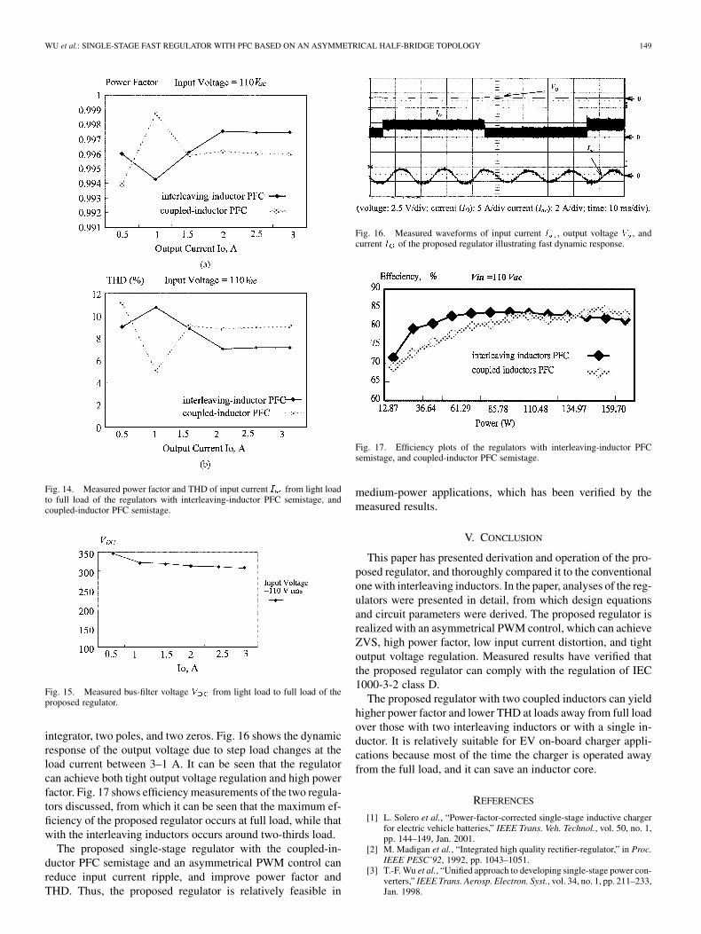
WU et al.: SINGLE-STAGE FAST REGULATOR WITH PFC BASED ON AN ASYMMETRICAL HALF-BRIDGE TOPOLOGY 149
Fig. 14. Measured power factor and THD of input current I from light loadto full load of the regulators with interleaving-inductor PFC semistage, andcoupled-inductor PFC semistage.
Fig. 15. Measured bus-filter voltage V from light load to full load of theproposed regulator.
integrator, two poles, and two zeros. Fig. 16 shows the dynamicresponse of the output voltage due to step load changes at theload current between 3–1 A. It can be seen that the regulatorcan achieve both tight output voltage regulation and high powerfactor. Fig. 17 shows efficiency measurements of the two regula-tors discussed, from which it can be seen that the maximum ef-ficiency of the proposed regulator occurs at full load, while thatwith the interleaving inductors occurs around two-thirds load.
The proposed single-stage regulator with the coupled-in-ductor PFC semistage and an asymmetrical PWM control canreduce input current ripple, and improve power factor andTHD. Thus, the proposed regulator is relatively feasible in
Fig. 16. Measured waveforms of input current I , output voltage V , andcurrent I of the proposed regulator illustrating fast dynamic response.
Fig. 17. Efficiency plots of the regulators with interleaving-inductor PFCsemistage, and coupled-inductor PFC semistage.
medium-power applications, which has been verified by themeasured results.
V. CONCLUSION
This paper has presented derivation and operation of the pro-posed regulator, and thoroughly compared it to the conventionalone with interleaving inductors. In the paper, analyses of the reg-ulators were presented in detail, from which design equationsand circuit parameters were derived. The proposed regulator isrealized with an asymmetrical PWM control, which can achieveZVS, high power factor, low input current distortion, and tightoutput voltage regulation. Measured results have verified thatthe proposed regulator can comply with the regulation of IEC1000-3-2 class D.
The proposed regulator with two coupled inductors can yieldhigher power factor and lower THD at loads away from full loadover those with two interleaving inductors or with a single in-ductor. It is relatively suitable for EV on-board charger appli-cations because most of the time the charger is operated awayfrom the full load, and it can save an inductor core.
REFERENCES
[1] L. Solero et al., “Power-factor-corrected single-stage inductive chargerfor electric vehicle batteries,” IEEE Trans. Veh. Technol., vol. 50, no. 1,pp. 144–149, Jan. 2001.
[2] M. Madigan et al., “Integrated high quality rectifier-regulator,” in Proc.IEEE PESC’92, 1992, pp. 1043–1051.
[3] T.-F. Wu et al., “Unified approach to developing single-stage power con-verters,” IEEE Trans. Aerosp. Electron. Syst., vol. 34, no. 1, pp. 211–233,Jan. 1998.

150 IEEE TRANSACTIONS ON INDUSTRIAL ELECTRONICS, VOL. 52, NO. 1, FEBRUARY 2005
[4] R. Redl et al., “A new family of single-stage isolated power-factorcorrectors with fast regulation of the output voltage,” in Proc. IEEEPESC’94, 1994, pp. 1137–1144.
[5] S. Korotkov et al., “Asymmetrical half-bridge in a single stage pfcAC/DC converter,” in Proc. IEEE APEC’97, 1997, pp. 484–488.
[6] R. Redl, “A new soft-switching DC/DC converter and its applicationin an off-line power supply with integral high-quality rectification,” inProc. PESC’96, 1996, pp. 402–407.
[7] J.-Y. Lee et al., “A new single-stage AC/DC converter with high effi-ciency and high power factor,” in Proc. 18th Int. TelecommunicationsEnergy Conf., 1996, pp. 263–270.
[8] J.-Y. Lee et al., “Design of high quality AC/DC converter with high ef-ficiency based on half bridge topology,” in Proc. IEEE PESC’98, 1998,pp. 1054–1060.
[9] T.-F. Wu and J.-C. Hung, “Development of ZVS single-stage isolatedconverters with a PFC feature based on asymmetrical half-bridgetopology,” in Proc. IEEE PESC’02, 2002, pp. 1363–1368.
[10] C. H. Chan and M. H. Pong, “Input current analysis of interleaved boostconverters operating in discontinues-inductor-current-mode,” in Proc.IEEE PESC’97, 1997, pp. 392–398.
[11] F. Tao and F. C. Lee, “An interleaved single-stage power-factor-correc-tion electronic ballast,” in Proc. IEEE APEC’00, 2000, pp. 617–623.
[12] , “A critical-conduction-mode single-stage power-factor-correctionelectronic ballast,” in Proc. IEEE APEC’00, 2000, pp. 603–609.
Tsai-Fu Wu (S’89–M’91–SM’98) received the B.S.degree in electronics engineering from NationalChiao-Tung University, Shin-Chu, Taiwan, R.O.C.,in 1983, the M.S. degree in electrical and computerengineering from Ohio University, Athens, in 1988,and the Ph.D. degree in electrical engineering andcomputer science from thre University of Illinois,Chicago, in 1992.
From 1985 to 1986, he was a System Engineer withSAMPO, Inc., Taiwan, R.O.C., developing and de-signing graphic terminals. He was a Teaching and
Research Assistant in the Department of Electrical Engineering and ComputerScience, University of Illinois, Chicago, from 1988 to 1992. Since 1993, hehas been with the Electrical Engineering Department, National Chung ChengUniversity, Chia-Yi, Taiwan, R.O.C., where he is currently a Professor and theDirector of the Power Electronics Applied Research Laboratory (PEARL). Hisresearch interests include developing and modeling of power converters, designof electronic dimming ballasts for fluorescent lamps, metal halide lamps andplasma display, and design of solar-panel-supplied inverters for grid connec-tion.
Dr. Wu is a Senior Member of the Chinese Institute of Engineers.
Jin-Chyuan Hung (S’99) was born in Taiwan,R.O.C. He received the B.S. degree in biomedicalengineering in 1990 from Chung Yuan ChristianUniversity, Chung-Li, Taiwan, R.O.C., and theM.S. degree in electrical engineering in 1997 fromNational Chung Cheng University, Chia-Yi, Taiwan,R.O.C., where he is currently working towardthe Ph.D. degree in the Department of ElectricalEngineering.
His research interests include development of soft-switching converter topologies, power-factor-correc-
tion technology, and chargers for electric vehicle.
Sheng-Yu Tseng was born in Taiwan, R.O.C., in1970. He received the B.S. degree in electricalengineering in 1992 from National Taipei Universityof Technology, Taipei, Taiwan, R.O.C., and theM.S. degree in electrical engineering in 1999 fromNational Chung Cheng University, Chia-Yi, Taiwan,R.O.C., where he is currently working towardthe Ph.D. degree in the Department of ElectricalEngineering.
His research interests include design ofswitching-mode power supplies, color plasma
display panel driving circuits, and pulsed voltage generators for transdermaldrug delivery or processing microbes.
Yaow-Ming Chen (S’96–M’98) received the B.S.degree from National Cheng-Kung University,Tainan, Taiwan, R.O.C., in 1989, and the M.S. andPh.D. degrees from the University of Missouri,Columbia, in 1993 and 1997, respectively, all inelectrical engineering.
From 1997 to 2000, he was with I-Shou Univer-sity, Taiwan, R.O.C., as an Assistant Professor. In2000, he joined National Chung Cheng University,Chia-Yi, Taiwan, R.O.C., where he is currently anAssistant Professor in the Department of Electrical
Engineering. His research interests include power electronic converters, powersystem harmonics and compensation, and intelligent control.
Dr. Chen is a Member of the IEEE Power Electronics and IEEE IndustrialElectronics Societies.