
Design and Implementation of a Single-Stage PFC Active ...
21
electronics Article Design and Implementation of a Single-Stage PFC Active-Clamp Flyback Converter with Dual Transformers Sen-Tung Wu * and Yu-Ting Cheng Citation: Wu, S.-T.; Cheng, Y.-T. Design and Implementation of a Single-Stage PFC Active-Clamp Flyback Converter with Dual Transformers. Electronics 2021, 10, 2588. https://doi.org/10.3390/ electronics10212588 Academic Editor: Nikolay Hinov Received: 24 September 2021 Accepted: 21 October 2021 Published: 22 October 2021 Publisher’s Note: MDPI stays neutral with regard to jurisdictional claims in published maps and institutional affil- iations. Copyright: © 2021 by the authors. Licensee MDPI, Basel, Switzerland. This article is an open access article distributed under the terms and conditions of the Creative Commons Attribution (CC BY) license (https:// creativecommons.org/licenses/by/ 4.0/). Department of Electrical Engineering, National Formosa University, No.64, Wunhua Rd., Taipei 632, Taiwan; [email protected] * Correspondence: [email protected]; Tel.: +886-5-631-5613 Abstract: This paper proposes an AC/DC single-stage structure by integrating a boost topology and an active clamp flyback (ACF) circuit with power-factor-correction (PFC) function. The PFC function can be achieved by controlling a boost PFC topology operated in the discontinuous conduction mode. With the coordination of active clamping components, a resonant technique is obtained and zero-voltage-switching (ZVS) can be achieved. The proposed converter is combined with the advantages of: (1) compared with two-stage circuit, a single stage circuit decreases the component of the main circuit and reduces the complexity of the control circuit; (2) a boost topology with PFC function operated in discontinuous conduction mode can be accomplished without adding any current detecting technique or detecting input signal; (3) by using the inductor from the PFC stage, ZVS function can be achieved without any additional inductor; (4) the increment of switching frequency facilitates the optimization of power density; (5) the conducting loss at the secondary side can be reduced by adding the synchronous rectification; (6) in this proposed scheme, the dual transformers with series-parallel connection are utilized, the current at the secondary side can be shared for lowering the conduction loss of the synchronous transistors. Finally, a prototype converter with AC 110 V input and DC 19 V/6.32 A (120 W) output under 300 kHz switching frequency is implemented. The efficiency of the proposed converter reaches 88.20% and 0.984 power factor in full load condition. Keywords: active clamp flyback; power-factor-correction; soft-switching 1. Introduction The development of civilization and the rapid advancement of science and technology have led to a shortage of our energy. The optimization of efficiency has become one of the main goals in power electronic industries; thus, many countries have begun to establish different kinds of standards for energies gradually. In addition to that, the dimension, the efficiency, and the power density of power supplies are much more a matter of concern today. Therefore, various topologies and control methods are proposed to improve the aforementioned issues widely. Flyback converters [1–3] are the most commonly used in low power electronics ap- plications and consumer products, such as smart phone chargers, adaptors for laptops, and electric scooter battery chargers. The active-clamp techniques [4–7] have improved several drawbacks of the conventional flyback converter topology. The additional clamping capacitor can absorb the energy which is stored in the leakage inductor [8]. This helps to reduce voltage spikes during switching conditions [9,10]. By designing the parameters of the leakage inductor and the clamping capacitor to resonate appropriately, ZVS can be achieved easily [11]. This technique not only releases the energy of leakage inductance efficiently, but also makes good use of it by achieving soft switching to reduce switching loss. To pursue higher power density, increasing switching frequency can reduce the size of the transformer and magnetic component. Thus, the soft switching technique is one of Electronics 2021, 10, 2588. https://doi.org/10.3390/electronics10212588 https://www.mdpi.com/journal/electronics
-
Upload
khangminh22 -
Category
Documents
-
view
0 -
download
0
Transcript of Design and Implementation of a Single-Stage PFC Active ...

electronics
Article
Design and Implementation of a Single-Stage PFCActive-Clamp Flyback Converter with Dual Transformers
Sen-Tung Wu * and Yu-Ting Cheng
Citation: Wu, S.-T.; Cheng, Y.-T.
Design and Implementation of a
Single-Stage PFC Active-Clamp
Flyback Converter with Dual
Transformers. Electronics 2021, 10,
2588. https://doi.org/10.3390/
electronics10212588
Academic Editor: Nikolay Hinov
Received: 24 September 2021
Accepted: 21 October 2021
Published: 22 October 2021
Publisher’s Note: MDPI stays neutral
with regard to jurisdictional claims in
published maps and institutional affil-
iations.
Copyright: © 2021 by the authors.
Licensee MDPI, Basel, Switzerland.
This article is an open access article
distributed under the terms and
conditions of the Creative Commons
Attribution (CC BY) license (https://
creativecommons.org/licenses/by/
4.0/).
Department of Electrical Engineering, National Formosa University, No.64, Wunhua Rd., Taipei 632, Taiwan;[email protected]* Correspondence: [email protected]; Tel.: +886-5-631-5613
Abstract: This paper proposes an AC/DC single-stage structure by integrating a boost topology andan active clamp flyback (ACF) circuit with power-factor-correction (PFC) function. The PFC functioncan be achieved by controlling a boost PFC topology operated in the discontinuous conductionmode. With the coordination of active clamping components, a resonant technique is obtainedand zero-voltage-switching (ZVS) can be achieved. The proposed converter is combined with theadvantages of: (1) compared with two-stage circuit, a single stage circuit decreases the componentof the main circuit and reduces the complexity of the control circuit; (2) a boost topology withPFC function operated in discontinuous conduction mode can be accomplished without addingany current detecting technique or detecting input signal; (3) by using the inductor from the PFCstage, ZVS function can be achieved without any additional inductor; (4) the increment of switchingfrequency facilitates the optimization of power density; (5) the conducting loss at the secondaryside can be reduced by adding the synchronous rectification; (6) in this proposed scheme, the dualtransformers with series-parallel connection are utilized, the current at the secondary side can beshared for lowering the conduction loss of the synchronous transistors. Finally, a prototype converterwith AC 110 V input and DC 19 V/6.32 A (120 W) output under 300 kHz switching frequency isimplemented. The efficiency of the proposed converter reaches 88.20% and 0.984 power factor in fullload condition.
Keywords: active clamp flyback; power-factor-correction; soft-switching
1. Introduction
The development of civilization and the rapid advancement of science and technologyhave led to a shortage of our energy. The optimization of efficiency has become one of themain goals in power electronic industries; thus, many countries have begun to establishdifferent kinds of standards for energies gradually. In addition to that, the dimension, theefficiency, and the power density of power supplies are much more a matter of concerntoday. Therefore, various topologies and control methods are proposed to improve theaforementioned issues widely.
Flyback converters [1–3] are the most commonly used in low power electronics ap-plications and consumer products, such as smart phone chargers, adaptors for laptops,and electric scooter battery chargers. The active-clamp techniques [4–7] have improvedseveral drawbacks of the conventional flyback converter topology. The additional clampingcapacitor can absorb the energy which is stored in the leakage inductor [8]. This helps toreduce voltage spikes during switching conditions [9,10]. By designing the parametersof the leakage inductor and the clamping capacitor to resonate appropriately, ZVS can beachieved easily [11]. This technique not only releases the energy of leakage inductanceefficiently, but also makes good use of it by achieving soft switching to reduce switchingloss. To pursue higher power density, increasing switching frequency can reduce the sizeof the transformer and magnetic component. Thus, the soft switching technique is one of
Electronics 2021, 10, 2588. https://doi.org/10.3390/electronics10212588 https://www.mdpi.com/journal/electronics

Electronics 2021, 10, 2588 2 of 21
the common ways to increase the switching frequency and the efficiency to a higher level.The synchronous rectification (SR) technique is also a trend to improve the efficiency ofconverters currently. The SR switch can be controlled by detecting the voltage across theSR switch at the secondary side. The switching period can be controlled appropriately.However, if the SR technique works perfectly and precisely, proper layout of the schematicand the good driving signal are necessary.
In addition to the better performance of converters’ efficiency, the power factor (PF)is also a key index to describe the ratio of real power and apparent power. Differentoutput load characteristics will cause the phase shift and deformation of the input currentwaveform. The increment of the reactive power from the AC main will increase the lossesof power line during the energy delivering process. Thus, the PFC technique [12,13] iswidely used to maintain the level of power factor and to fulfill the electrical specificationsof power supplies. It can be classified into passive and active [14–16] methods. The passivemethod is mainly realized by passive components which has a low cost but large size. Theeffect of power factor correction is also limited; active methods use the additional switchand circuit to make the input current and voltage waveform in phase to improve powerfactor. By using this technique, PF can approach 1 with low harmonic. The effect of theactive method is much better than that of the passive one, but this method requires oneindependent circuit with control stage to achieve. That requires more components and thecost will also increase
In general, the structure of AC-DC converter with PFC function is a two-stage topology.It can be divided by two independent circuits [17,18]. Both of the independent circuitsneed to be operated by their own control systems. Hence, the number of components willdefinitely be increased. In order to simplify the structure of the two-stage circuit [19,20],the single-stage architecture was proposed.
In reference [21], a boost converter and a flyback converter with valley switching werecombined. With the valley switching technique, switching loss is reduced by detectingauxiliary winding. The secondary side synchronous rectification is achieved through theself-made detection mechanism for increasing overall efficiency. However, it is difficultfor the power factor to exceed 0.9, and the voltage spike problem of VDS is the obstacle fordeveloping toward a higher frequency level. Reference [22] combined a boost converterwith a low-side ACF converter. Soft switching can be used to increase the switchingfrequency and efficiency. P-channel MOSFET can be utilized to solve the isolation issuefor high-side switch in ACF topology. However, it is not common for P-channel MOSFETto have a high withstanding voltage in practical. An external inductor is also needed toachieve ZVS which increases the elements of the circuit. In reference [23], an interleavedPFC boost converter is proposed and the efficiency goes to 95% under 110 V AC input.Reference [24] proposed an ACF converter with 93% of efficiency under 120 W outputcondition. The overall efficiency reached about 88.35% if the ACF and PFC stages wereconnected. Reference [25] proposed integrating a bridgeless boost and a LLC converter.ZVS and ZCS are achieved under different conditions, but several diodes are required toprevent the wrong current direction. Thus, an external inductor is also needed in the LLCresonant tank of the circuit. It also increases the total component of the circuit. In [26], anovel high-gain DC-DC boost converter with lower component count was implemented.This novel boost converter has higher power density characteristics which is suitable forthe smaller size of electronic product with PFC function to boost the voltage for 400 Vdcapplications. Lower component counts also bring lower cost and loss.
To compare with previous studies, several papers have proposed a single-stage PFCconverter with soft-switching technique. From [26–29], they provided different kinds of single-stage structures, and they have different benefits and features individually. In reference [27],the number of switches is one, thus the switching loss is low. In reference [28,29], the numberof switches is two. The switching losses are still low, but the performances of THD for thesethree references are moderate or even higher. For the proposed circuit, two of the switchesare used for PFC and ACF functions, the other two switchers are used for synchronous

Electronics 2021, 10, 2588 3 of 21
rectification for decreasing the conduction loss, and THD performs well among thesestudies. Table 1 shows a comparison of the related studies.
Table 1. Comparison of the related single-stage converter with soft-switching function.
Item and No. Proposed Ref. [26] Ref. [27] Ref. [28] Ref. [29]
Switch 4 1 1 2 2Inductor 2 2 1 3 1Diode 4 3 3 4 5Capacitor 4 2 3 4 5Windings 2 n/a 3 4 2THD Low n/a Moderate High ModerateSwitching loss Moderate Low Low Low LowEfficiency(%) 88.2 92.0 91.5 91.3 91.0
To combine with the PFC stage and the DC-DC converter into one simple circuit isthe main concept of this paper. It not only reduces the number of components, but alsodelivers the energy to the output load directly. The proposed paper is to combine the PFCtechnique and ACF converter into the single-stage structure. The goal of this paper is tosimplify the structure and also to implement the single-stage PFC and ACF converter withdual transformer. In this proposed circuit, the dual transformers with series input andparallel output connection were selected. The benefit of this connection is that each of thetransformers only needs to deliver half of the power from input to the output load. Thelarger inductance causes smaller current variation on Lm. This situation can reduce thepeak value and effective value of the primary side current. To compare with the volumeof a single winding transformer, the dual transformers are indeed larger than the singleone. However, the diameter of copper wire and the size of magnetic core can be smallerfor dual transformer topology. In addition, the synchronous mechanism can reduce theconduction loss effectively. To sum up the characteristics and the functions above, theproposed topology is suitable for higher power demand adaptor applications, such asgaming laptops and mini-computers.
2. Proposed AC-DC Converter2.1. The Proposed Circuit Structure
In this paper, a single-stage circuit with AC input and DC output was developed asshown in Figure 1. The proposed design utilizes a PFC boost topology to combine with theactive clamp flyback converter without any external resonant inductor [9]. The clampingcapacitor CClamp can be shared as the common current path for both stages to reduce thenumber of main circuit components. The PFC stage is operated under discontinuousconduction mode for full range to lower the complexity of the PFC control method. Dueto the characteristics of active clamping technique, ZVS can be easily achieved on bothswitches S1 and S2 at the primary side. In addition to that, the dual transformer connectionand the synchronous rectification technique at the secondary side can reduce the conductionloss effectively.
2.2. Principle of Operation
Since the AC input voltage passes through a full-bridge rectifier, no matter whetherthe input voltage is positive or negative, the output voltage of the rectifier is still positive.Therefore, the following description will only focus on the positive waveform duration.As shown in Figure 2, due to the topology of the circuit, the sinusoidal waveform changesas the value of |vin(t)| changes. The waveform can be divided into the valley, the middle,and the peak point. The valley point means that the rectified voltage drops to 0 V and thisvalley point is operated as a conventional active clamp flyback converter. The peak pointsare influenced by the value of |vin(t)| the most. For the time axis, π
2 and 3π2 are the peak

Electronics 2021, 10, 2588 4 of 21
points of the rectified voltage. The middle points are located between the valley and thepeak points which are at π
4 and 3π4 of the time axis.
Electronics 2021, 10, 2588 4 of 21
Figure 1. Topology of the proposed circuit.
2.2. Principle of Operation Since the AC input voltage passes through a full-bridge rectifier, no matter whether
the input voltage is positive or negative, the output voltage of the rectifier is still positive. Therefore, the following description will only focus on the positive waveform duration. As shown in Figure 2, due to the topology of the circuit, the sinusoidal waveform changes as the value of |𝑣 (𝑡)| changes. The waveform can be divided into the valley, the middle, and the peak point. The valley point means that the rectified voltage drops to 0 V and this valley point is operated as a conventional active clamp flyback converter. The peak points are influenced by the value of |𝑣 (𝑡)| the most. For the time axis, and are the peak points of the rectified voltage. The middle points are located between the valley and the peak points which are at and of the time axis.
Figure 2. Output voltage from the rectifier circuit.
After the definition of these critical points, the operation modes of the circuit will be discussed in this section. The current path of the primary side and the secondary side will be illustrated in different colors. The blue shows the power factor correction path. The red shows the active clamp current path. The green shows the current at the secondary side. These current paths help to simplify the following explanation, and the theoretical paths are shown in Figure 3.
CBus
LrLPFC
COSS3
COSS4NP2:NS2T2
Cin
+-
S2 vDS2vGS2
COSS2
DS2
CClampvClamp
VBus
Lm1
Lm2
vGS3
vGS4
vDS4
vDS3
DS3
DS4
VCoCO
VORO
D1
D2
D3
D4
iin
iLPFC
iDS1
iLr
iLm1iClamp
iDS2
iSD3
iSD4
IO
vin
COSS1vDS1
VGS1
DS1 NP1:NS1T1
iLm2
Power Factor Correction Part Active Clamp Flyback Part
Figure 1. Topology of the proposed circuit.
Electronics 2021, 10, 2588 4 of 21
Figure 1. Topology of the proposed circuit.
2.2. Principle of Operation Since the AC input voltage passes through a full-bridge rectifier, no matter whether
the input voltage is positive or negative, the output voltage of the rectifier is still positive. Therefore, the following description will only focus on the positive waveform duration. As shown in Figure 2, due to the topology of the circuit, the sinusoidal waveform changes as the value of |𝑣 (𝑡)| changes. The waveform can be divided into the valley, the middle, and the peak point. The valley point means that the rectified voltage drops to 0 V and this valley point is operated as a conventional active clamp flyback converter. The peak points are influenced by the value of |𝑣 (𝑡)| the most. For the time axis, and are the peak points of the rectified voltage. The middle points are located between the valley and the peak points which are at and of the time axis.
Figure 2. Output voltage from the rectifier circuit.
After the definition of these critical points, the operation modes of the circuit will be discussed in this section. The current path of the primary side and the secondary side will be illustrated in different colors. The blue shows the power factor correction path. The red shows the active clamp current path. The green shows the current at the secondary side. These current paths help to simplify the following explanation, and the theoretical paths are shown in Figure 3.
CBus
LrLPFC
COSS3
COSS4NP2:NS2T2
Cin
+-
S2 vDS2vGS2
COSS2
DS2
CClampvClamp
VBus
Lm1
Lm2
vGS3
vGS4
vDS4
vDS3
DS3
DS4
VCoCO
VORO
D1
D2
D3
D4
iin
iLPFC
iDS1
iLr
iLm1iClamp
iDS2
iSD3
iSD4
IO
vin
COSS1vDS1
VGS1
DS1 NP1:NS1T1
iLm2
Power Factor Correction Part Active Clamp Flyback Part
Figure 2. Output voltage from the rectifier circuit.
After the definition of these critical points, the operation modes of the circuit will bediscussed in this section. The current path of the primary side and the secondary side willbe illustrated in different colors. The blue shows the power factor correction path. The redshows the active clamp current path. The green shows the current at the secondary side.These current paths help to simplify the following explanation, and the theoretical pathsare shown in Figure 3.
2.2.1. Mode 1—(t0 < t < t1)
As shown in Figure 4, due to the previous mode, the high side switch’s parasiticcapacitor COSS1 is discharged to zero and then S1 turns on in this mode. ZVS of S1 canbe achieved. At the beginning of this mode, the total leakage inductor Lr, the magneticinductors Lm1 and Lm2 keep the same current direction and charge to CBus as the previousstate. The energy stored in the power factor correction inductor LPFC also charges to thecapacitor CBus at the same time. When the energy stored in Lr, Lm1, and Lm2 are released,the current direction of these inductors turns to be positive and starts to be charged. Whenthe charging process of CBus ends, the coming operation mode will be carried out. In thismode, there is no energy delivered to the secondary side. The switches S3 and S4 at thesecondary side are turned off; hence, the energy of the output load RO is provided by theoutput capacitor Co. Through the analysis above, Equations (1) and (2) can be obtainedbelow. ω1 is the angular frequency of the AC input voltage. In this mode, the angularfrequency ω and the impedance Z are also shown in Equation (3).

Electronics 2021, 10, 2588 5 of 21
iLPFC(t) = iLPFC(t0)· cos ω(t− t0) +
[|Vm· sin ω1(t− t0)| −VBus − vClamp(t0)
]· sin ω(t− t0)
Z(1)
vClamp(t) =[|Vm· sin ω(t− t0)| −VBus − vClamp(t0)
]·(1− cos ω(t− t0)) + Z·iLPFC(t0)· sin ω(t− t0) (2)
ω =1√
LPFC·CClamp
; Z =
√LPFC
CClamp(3)Electronics 2021, 10, 2588 5 of 21
Figure 3. The related key waveforms of the proposed circuit.
2.2.1. Mode 1—(t0 < t < t1) As shown in Figure 4, due to the previous mode, the high side switch’s parasitic ca-
pacitor COSS1 is discharged to zero and then S1 turns on in this mode. ZVS of S1 can be achieved. At the beginning of this mode, the total leakage inductor Lr, the magnetic induc-tors Lm1 and Lm2 keep the same current direction and charge to CBus as the previous state. The energy stored in the power factor correction inductor LPFC also charges to the capacitor CBus at the same time. When the energy stored in Lr, Lm1, and Lm2 are released, the current direction of these inductors turns to be positive and starts to be charged. When the charg-ing process of CBus ends, the coming operation mode will be carried out. In this mode, there is no energy delivered to the secondary side. The switches S3 and S4 at the secondary side are turned off; hence, the energy of the output load RO is provided by the output capacitor Co. Through the analysis above, Equations (1) and (2) can be obtained below. ω1 is the angular frequency of the AC input voltage. In this mode, the angular frequency ω and the impedance Z are also shown in Equation (3). 𝑖 (𝑡) = 𝑖 (𝑡 ) ∙ cos 𝜔(𝑡 − 𝑡 ) + | ∙ ( )| ( ) ∙ ( ) (1) 𝑣 (𝑡) = |𝑉 ∙ 𝑠𝑖𝑛 𝜔(𝑡 − 𝑡 )| − 𝑉 − 𝑣 (𝑡 ) ∙ (1 − cos 𝜔(𝑡 − 𝑡 )) + 𝑍 ∙ 𝑖 (𝑡 ) ∙ sin 𝜔(𝑡 − 𝑡 ) (2) 𝜔 = ∙ ; 𝑍 = (3)
Figure 3. The related key waveforms of the proposed circuit.
2.2.2. Mode 2—(t1 < t < t2)
As shown in Figure 5, in this mode, S1 still turns on. LPFC continues releasing theenergy and charging to the clamping capacitor CClamp from mode 1. LPFC also charges toLr, Lm1, and Lm2. In the meantime, CBus also charges to Lr, Lm1, and Lm2 through S1. Whenthe energy of LPFC is exhausted, iLPFC drops to 0 A. Thus, VClamp starts to be clamped at aconstant voltage temporarily. This mode ends when S1 is turned off.

Electronics 2021, 10, 2588 6 of 21Electronics 2021, 10, 2588 6 of 21
Figure 4. Current route of Mode 1.
2.2.2. Mode 2—(t1 < t < t2) As shown in Figure 5, in this mode, S1 still turns on. LPFC continues releasing the en-
ergy and charging to the clamping capacitor CClamp from mode 1. LPFC also charges to Lr, Lm1, and Lm2. In the meantime, CBus also charges to Lr, Lm1, and Lm2 through S1. When the energy of LPFC is exhausted, iLPFC drops to 0 A. Thus, VClamp starts to be clamped at a constant voltage temporarily. This mode ends when S1 is turned off.
Figure 5. Current route of Mode 2.
2.2.3. Mode 3—(t2 < t < t3) As shown in Figure 6, during the dead time, COSS1 is charged by the path of CBus. The
charging path will be open when COSS1 is charged to the sum of VBus and vClamp. Since Lr, Lm1, and Lm2 maintain the same current direction from the previous step, the energy on COSS2 will be taken away while the current goes through S2. After COSS2’s energy releases to zero, S2’s body diode DS2 will be turned on to maintain the negative current path. This mode ends when dead time is finished. In this step, no energy is transmitted to the secondary side. The secondary side switches S3 and S4 are turned off, the energy of the output load RO is provided by the output capacitor Co. Equation (4) can be analyzed through this step; ω and Z’s equation are shown in (5). 𝑖 (𝑡) = 𝑖 (𝑡 ) ∙ cos 𝜔(𝑡 − 𝑡 ) + ∙ ( ) (4)𝜔 = ( )∙( ) ; 𝑍 = (5)
Figure 4. Current route of Mode 1.
Electronics 2021, 10, 2588 6 of 21
Figure 4. Current route of Mode 1.
2.2.2. Mode 2—(t1 < t < t2) As shown in Figure 5, in this mode, S1 still turns on. LPFC continues releasing the en-
ergy and charging to the clamping capacitor CClamp from mode 1. LPFC also charges to Lr, Lm1, and Lm2. In the meantime, CBus also charges to Lr, Lm1, and Lm2 through S1. When the energy of LPFC is exhausted, iLPFC drops to 0 A. Thus, VClamp starts to be clamped at a constant voltage temporarily. This mode ends when S1 is turned off.
Figure 5. Current route of Mode 2.
2.2.3. Mode 3—(t2 < t < t3) As shown in Figure 6, during the dead time, COSS1 is charged by the path of CBus. The
charging path will be open when COSS1 is charged to the sum of VBus and vClamp. Since Lr, Lm1, and Lm2 maintain the same current direction from the previous step, the energy on COSS2 will be taken away while the current goes through S2. After COSS2’s energy releases to zero, S2’s body diode DS2 will be turned on to maintain the negative current path. This mode ends when dead time is finished. In this step, no energy is transmitted to the secondary side. The secondary side switches S3 and S4 are turned off, the energy of the output load RO is provided by the output capacitor Co. Equation (4) can be analyzed through this step; ω and Z’s equation are shown in (5). 𝑖 (𝑡) = 𝑖 (𝑡 ) ∙ cos 𝜔(𝑡 − 𝑡 ) + ∙ ( ) (4)𝜔 = ( )∙( ) ; 𝑍 = (5)
Figure 5. Current route of Mode 2.
2.2.3. Mode 3—(t2 < t < t3)
As shown in Figure 6, during the dead time, COSS1 is charged by the path of CBus. Thecharging path will be open when COSS1 is charged to the sum of VBus and vClamp. SinceLr, Lm1, and Lm2 maintain the same current direction from the previous step, the energyon COSS2 will be taken away while the current goes through S2. After COSS2’s energyreleases to zero, S2’s body diode DS2 will be turned on to maintain the negative currentpath. This mode ends when dead time is finished. In this step, no energy is transmitted tothe secondary side. The secondary side switches S3 and S4 are turned off, the energy ofthe output load RO is provided by the output capacitor Co. Equation (4) can be analyzedthrough this step; ω and Z’s equation are shown in (5).
iLr(t) = iLr(t2)· cos ω(t− t2) +VBus· sin ω(t− t2)
Z(4)
ω =1√
(Lr + 2Lm)·(CCOSS1 + CCOSS2); Z =
√Lr + 2Lm
CCOSS1 + CCOSS2(5)

Electronics 2021, 10, 2588 7 of 21Electronics 2021, 10, 2588 7 of 21
Figure 6. Current route of Mode 3.
2.2.4. Mode 4—(t3 < t < t4) As shown in Figure 7, due to the previous mode, the low side switch’s capacitor COSS2
is released to zero during the switching of S2 in this mode. S2’s ZVS can be achieved. LPFC will be charged by input AC power. Lr and CClamp start to resonate with each other, the next mode begins when Lr releases its energy to zero. The magnetizing inductors Lm1 and Lm2 transfer energy to secondary side, vGS3 and vGS4 turn high to achieve synchronous rectifi-cation function to reduce losses of S3 and S4. Equations (6) and (7) can be analyzed through this step; ω and Z’s equation are shown in (8). 𝑖 (𝑡) = 𝑖 (𝑡 ) ∙ cos 𝜔(𝑡 − 𝑡 ) + ∙ ∙ ( ) ∙ ( )
(6) 𝑣 (𝑡) = 2 ∙ 𝑛 ∙ 𝑉 − 𝑣 (𝑡 ) ∙ (1 − cos 𝜔(𝑡 − 𝑡 ) ) + 𝑍 ∙ 𝑖 (𝑡 ) ∙ sin 𝜔(𝑡 − 𝑡 ) (7)𝜔 = ∙ ; 𝑍 = (8)
Figure 7. Current route of Mode 4.
2.2.5. Mode 5—(t4 < t < t5) As shown in Figure 8, due to the exhaustion of Lr, CClamp releases its energy to Lr. Both
components keep resonating with the opposite current direction as shown in mode 4. Lm1 and Lm2 release their energy to secondary side at the beginning of this step. When both of the magnetizing inductors release to zero, CClamp will transfer its energy to Lm1, Lm2, and the secondary side. The current direction of iLm1 and iLm2 will be opposite to the beginning of this step. Lm1 and Lm2 transfer energy to secondary at the beginning of this step, CClamp will keep transferring when the magnetizing inductors are out of energy. vGS3 and vGS4 remain high to achieve synchronous rectification function for reducing losses of S3 and S4. Equa-tions (9) and (10) can be analyzed through this step; ω and Z’s equation are shown in (11). 𝑖 (𝑡) = −𝑖 (𝑡 ) ∙ cos𝜔(𝑡 − 𝑡 ) + ∙ ∙ ( ) ∙ ( )
(9)
Figure 6. Current route of Mode 3.
2.2.4. Mode 4—(t3 < t < t4)
As shown in Figure 7, due to the previous mode, the low side switch’s capacitor COSS2is released to zero during the switching of S2 in this mode. S2’s ZVS can be achieved. LPFCwill be charged by input AC power. Lr and CClamp start to resonate with each other, thenext mode begins when Lr releases its energy to zero. The magnetizing inductors Lm1 andLm2 transfer energy to secondary side, vGS3 and vGS4 turn high to achieve synchronousrectification function to reduce losses of S3 and S4. Equations (6) and (7) can be analyzedthrough this step; ω and Z’s equation are shown in (8).
iLr(t) = iLr(t3)· cos[ω(t− t3)] +
[2·n·VO − vClamp(t3)
]· sin[ω(t− t3)]
Z(6)
vClamp(t) =[2·n·VO − vClamp(t3)
]·(1− cos[ω(t− t3)]) + Z·iLr(t3)· sin[ω(t− t3)] (7)
ω =1√
Lr·CClamp
; Z =
√Lr
CClamp(8)
Electronics 2021, 10, 2588 7 of 21
Figure 6. Current route of Mode 3.
2.2.4. Mode 4—(t3 < t < t4) As shown in Figure 7, due to the previous mode, the low side switch’s capacitor COSS2
is released to zero during the switching of S2 in this mode. S2’s ZVS can be achieved. LPFC will be charged by input AC power. Lr and CClamp start to resonate with each other, the next mode begins when Lr releases its energy to zero. The magnetizing inductors Lm1 and Lm2 transfer energy to secondary side, vGS3 and vGS4 turn high to achieve synchronous rectifi-cation function to reduce losses of S3 and S4. Equations (6) and (7) can be analyzed through this step; ω and Z’s equation are shown in (8). 𝑖 (𝑡) = 𝑖 (𝑡 ) ∙ cos 𝜔(𝑡 − 𝑡 ) + ∙ ∙ ( ) ∙ ( )
(6) 𝑣 (𝑡) = 2 ∙ 𝑛 ∙ 𝑉 − 𝑣 (𝑡 ) ∙ (1 − cos 𝜔(𝑡 − 𝑡 ) ) + 𝑍 ∙ 𝑖 (𝑡 ) ∙ sin 𝜔(𝑡 − 𝑡 ) (7)𝜔 = ∙ ; 𝑍 = (8)
Figure 7. Current route of Mode 4.
2.2.5. Mode 5—(t4 < t < t5) As shown in Figure 8, due to the exhaustion of Lr, CClamp releases its energy to Lr. Both
components keep resonating with the opposite current direction as shown in mode 4. Lm1 and Lm2 release their energy to secondary side at the beginning of this step. When both of the magnetizing inductors release to zero, CClamp will transfer its energy to Lm1, Lm2, and the secondary side. The current direction of iLm1 and iLm2 will be opposite to the beginning of this step. Lm1 and Lm2 transfer energy to secondary at the beginning of this step, CClamp will keep transferring when the magnetizing inductors are out of energy. vGS3 and vGS4 remain high to achieve synchronous rectification function for reducing losses of S3 and S4. Equa-tions (9) and (10) can be analyzed through this step; ω and Z’s equation are shown in (11). 𝑖 (𝑡) = −𝑖 (𝑡 ) ∙ cos𝜔(𝑡 − 𝑡 ) + ∙ ∙ ( ) ∙ ( )
(9)
Figure 7. Current route of Mode 4.
2.2.5. Mode 5—(t4 < t < t5)
As shown in Figure 8, due to the exhaustion of Lr, CClamp releases its energy to Lr. Bothcomponents keep resonating with the opposite current direction as shown in mode 4. Lm1and Lm2 release their energy to secondary side at the beginning of this step. When both ofthe magnetizing inductors release to zero, CClamp will transfer its energy to Lm1, Lm2, and thesecondary side. The current direction of iLm1 and iLm2 will be opposite to the beginning of thisstep. Lm1 and Lm2 transfer energy to secondary at the beginning of this step, CClamp will keeptransferring when the magnetizing inductors are out of energy. vGS3 and vGS4 remain high to

Electronics 2021, 10, 2588 8 of 21
achieve synchronous rectification function for reducing losses of S3 and S4. Equations (9) and(10) can be analyzed through this step; ω and Z’s equation are shown in (11).
iLr(t) = −iLr(t4)· cos ω(t− t4) +
[2·n·VO − vClamp(t4)
]· sin ω(t− t4)
Z(9)
vClamp(t)=[2·n·VO − vClamp(t4)
]·(1− cos ω(t− t4)) + Z·iLr(t4)· sin ω(t− t4) (10)
1√Lr·CClamp
; Z =
√Lr
CClamp(11)
Electronics 2021, 10, 2588 8 of 21
𝑣 (𝑡) = 2 ∙ 𝑛 ∙ 𝑉 − 𝑣 (𝑡 ) ∙ 1 − cos𝜔(𝑡 − 𝑡 ) + 𝑍 ∙ 𝑖 (𝑡 ) ∙ sin 𝜔(𝑡 − 𝑡 ) (10)
∙ ; 𝑍 = (11)
Figure 8. Current route of Mode 5.
2.2.6. Mode 6—(t5 < t < t6) As shown in Figure 9, during the dead time, COSS2 starts to be charged. The charging
path is open when COSS2 is charged to the sum of VBus and vClamp. Since Lr, Lm1, and Lm2 main-tain the same current direction from the previous step, the energy on COSS1 will be taken away during the current went through S1. After COSS1’s energy releases to zero, S2’s body diode DS2 is turned on to maintain the negative current path. In this mode, LPFC starts to discharge and to release energy to CClamp, CBus, and COSS2. COSS1 also discharges at the same time. This mode ends when dead time is finished. CClamp keeps transferring energy to sec-ondary side. vGS3 and vGS4 remain high to achieve synchronous rectification function. Equa-tion (12) can be analyzed through this step; ω and Z’s equation are shown in Equation (13). 𝑖 (𝑡) = ∙ ∙ ( ) ∙ ( ) − 𝑖 (𝑡 ) ∙ cos 𝜔(𝑡 − 𝑡 ) (12)
𝜔 = ∙( ) ; 𝑍 = (13)
Figure 9. Current route of Mode 6.
2.3. Design Consideration In order to simplify the design of single-stage architecture, the power factor correc-
tion inductor is designed to operate under discontinuous conduction mode [10,11]. The extra input voltage or current signal detection mechanism for continuous conduction mode or boundary conduction mode [12,13] can be removed. In the case of discontinuous conduction mode, Figure 10 can be drawn. The relationship of iLPFC during the on and off
Figure 8. Current route of Mode 5.
2.2.6. Mode 6—(t5 < t < t6)
As shown in Figure 9, during the dead time, COSS2 starts to be charged. The chargingpath is open when COSS2 is charged to the sum of VBus and vClamp. Since Lr, Lm1, and Lm2maintain the same current direction from the previous step, the energy on COSS1 will betaken away during the current went through S1. After COSS1’s energy releases to zero, S2’sbody diode DS2 is turned on to maintain the negative current path. In this mode, LPFCstarts to discharge and to release energy to CClamp, CBus, and COSS2. COSS1 also dischargesat the same time. This mode ends when dead time is finished. CClamp keeps transferringenergy to secondary side. vGS3 and vGS4 remain high to achieve synchronous rectificationfunction. Equation (12) can be analyzed through this step; ω and Z’s equation are shownin Equation (13).
iLr(t) =
[2·n·VO − vClamp(t5)
]· sin ω(t− t5)
Z− iLr(t5)· cos ω(t− t5) (12)
ω =1√
Lr·(CCOSS1 + CCOSS2); Z =
√Lr
CCOSS1 + CCOSS2(13)
2.3. Design Consideration
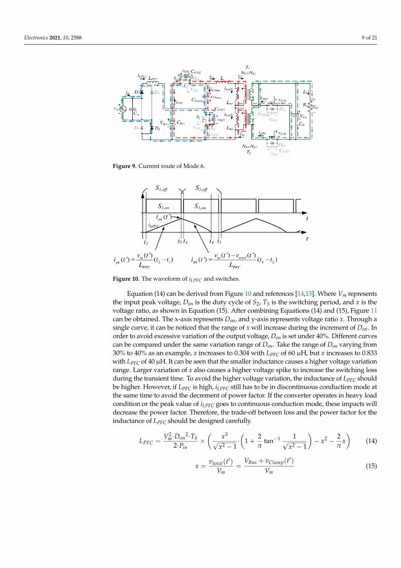
In order to simplify the design of single-stage architecture, the power factor correctioninductor is designed to operate under discontinuous conduction mode [10,11]. The extrainput voltage or current signal detection mechanism for continuous conduction modeor boundary conduction mode [12,13] can be removed. In the case of discontinuousconduction mode, Figure 10 can be drawn. The relationship of iLPFC during the on and offtime of the power switch can be obtained through the operation process, where vtotal(t’)represents VBus + vClamp(t’).
Electronics 2021, 10, 2588 9 of 21
Electronics 2021, 10, 2588 8 of 21
𝑣 (𝑡) = 2 ∙ 𝑛 ∙ 𝑉 − 𝑣 (𝑡 ) ∙ 1 − cos𝜔(𝑡 − 𝑡 ) + 𝑍 ∙ 𝑖 (𝑡 ) ∙ sin 𝜔(𝑡 − 𝑡 ) (10)
∙ ; 𝑍 = (11)
Figure 8. Current route of Mode 5.
2.2.6. Mode 6—(t5 < t < t6) As shown in Figure 9, during the dead time, COSS2 starts to be charged. The charging
path is open when COSS2 is charged to the sum of VBus and vClamp. Since Lr, Lm1, and Lm2 main-tain the same current direction from the previous step, the energy on COSS1 will be taken away during the current went through S1. After COSS1’s energy releases to zero, S2’s body diode DS2 is turned on to maintain the negative current path. In this mode, LPFC starts to discharge and to release energy to CClamp, CBus, and COSS2. COSS1 also discharges at the same time. This mode ends when dead time is finished. CClamp keeps transferring energy to sec-ondary side. vGS3 and vGS4 remain high to achieve synchronous rectification function. Equa-tion (12) can be analyzed through this step; ω and Z’s equation are shown in Equation (13). 𝑖 (𝑡) = ∙ ∙ ( ) ∙ ( ) − 𝑖 (𝑡 ) ∙ cos 𝜔(𝑡 − 𝑡 ) (12)
𝜔 = ∙( ) ; 𝑍 = (13)
Figure 9. Current route of Mode 6.
2.3. Design Consideration In order to simplify the design of single-stage architecture, the power factor correc-
tion inductor is designed to operate under discontinuous conduction mode [10,11]. The extra input voltage or current signal detection mechanism for continuous conduction mode or boundary conduction mode [12,13] can be removed. In the case of discontinuous conduction mode, Figure 10 can be drawn. The relationship of iLPFC during the on and off
Figure 9. Current route of Mode 6.
Electronics 2021, 10, 2588 9 of 21
time of the power switch can be obtained through the operation process, where vtotal(t’) represents VBus + vClamp(t’).
Figure 10. The waveform of iLPFC and switches.
Equation (14) can be derived from Figure 10 and references [14,15]. Where Vm repre-sents the input peak voltage, Don is the duty cycle of S2, TS is the switching period, and x is the voltage ratio, as shown in Equation (15). After combining Equations (14) and (15), Figure 11 can be obtained. The x-axis represents Don, and y-axis represents voltage ratio x. Through a single curve, it can be noticed that the range of x will increase during the incre-ment of Don. In order to avoid excessive variation of the output voltage, Don is set under 40%. Different curves can be compared under the same variation range of Don. Take the range of Don varying from 30% to 40% as an example, x increases to 0.304 with LPFC of 60 μH, but x increases to 0.833 with LPFC of 40 μH. It can be seen that the smaller inductance causes a higher voltage variation range. Larger variation of x also causes a higher voltage spike to increase the switching loss during the transient time. To avoid the higher voltage variation, the inductance of LPFC should be higher. However, if LPFC is high, iLPFC still has to be in discontinuous conduction mode at the same time to avoid the decrement of power factor. If the converter operates in heavy load condition or the peak value of iLPFC goes to continuous conduction mode, these impacts will decrease the power factor. Therefore, the trade-off between loss and the power factor for the inductance of LPFC should be designed carefully.
𝐿 = ∙ ∙∙ × √ ∙ 1 + tan √ − 𝑥 − 𝑥 (14)𝑥 = ( ) = ( ′) (15)
Figure 10. The waveform of iLPFC and switches.
Equation (14) can be derived from Figure 10 and references [14,15]. Where Vm representsthe input peak voltage, Don is the duty cycle of S2, TS is the switching period, and x is thevoltage ratio, as shown in Equation (15). After combining Equations (14) and (15), Figure 11can be obtained. The x-axis represents Don, and y-axis represents voltage ratio x. Through asingle curve, it can be noticed that the range of x will increase during the increment of Don. Inorder to avoid excessive variation of the output voltage, Don is set under 40%. Different curvescan be compared under the same variation range of Don. Take the range of Don varying from30% to 40% as an example, x increases to 0.304 with LPFC of 60 µH, but x increases to 0.833with LPFC of 40 µH. It can be seen that the smaller inductance causes a higher voltage variationrange. Larger variation of x also causes a higher voltage spike to increase the switching lossduring the transient time. To avoid the higher voltage variation, the inductance of LPFC shouldbe higher. However, if LPFC is high, iLPFC still has to be in discontinuous conduction mode atthe same time to avoid the decrement of power factor. If the converter operates in heavy loadcondition or the peak value of iLPFC goes to continuous conduction mode, these impacts willdecrease the power factor. Therefore, the trade-off between loss and the power factor for theinductance of LPFC should be designed carefully.
LPFC =V2
m·Don2·TS
2·Pin×(
x3√
x2 − 1·(
1 +2π
tan−1 1√x2 − 1
)− x2 − 2
πx)
(14)
x =vtotal(t′)
Vm=
VBus + vClamp(t′)Vm
(15)

Electronics 2021, 10, 2588 10 of 21Electronics 2021, 10, 2588 10 of 21
Figure 11. Relationship between Don and x.
To compare with the conventional boost topology for single stage structure [16], the power factor correction stage includes CClamp in the proposed topology. Figure 12 can be obtained through Equation (2) under different vin. Noticing vClamp is influenced by vin, the value of vDS1 and vDS2 will be influenced as well. Therefore, the value of CClamp is related to the switching loss of the primary switches. In Figure 12, the x-axis represents the time and the y-axis represents vClamp.
Figure 12. Relationship between vClamp and vin.
CClamp and Lr are the main resonant components when S2 turns on. The resonant period Tr between the two elements is about twice of the turn-on time when S2 is on as shown in Equation (16). CClamp will affect the switching loss and the capacitance of CClamp can be fur-ther optimized by SIMetrix software. As shown in Figure 13a, the smaller capacitance can reduce the switching loss of S2. In the meanwhile, from Figure 13b, this will also increase the conduction loss of the synchronous rectifier switch at the secondary side. That is, the smaller capacitance causes higher current at the secondary side. Therefore, the capacitance selection of CClamp should be considered carefully.
Figure 11. Relationship between Don and x.
To compare with the conventional boost topology for single stage structure [16], thepower factor correction stage includes CClamp in the proposed topology. Figure 12 can beobtained through Equation (2) under different vin. Noticing vClamp is influenced by vin, thevalue of vDS1 and vDS2 will be influenced as well. Therefore, the value of CClamp is relatedto the switching loss of the primary switches. In Figure 12, the x-axis represents the timeand the y-axis represents vClamp.
Electronics 2021, 10, 2588 10 of 21
Figure 11. Relationship between Don and x.
To compare with the conventional boost topology for single stage structure [16], the power factor correction stage includes CClamp in the proposed topology. Figure 12 can be obtained through Equation (2) under different vin. Noticing vClamp is influenced by vin, the value of vDS1 and vDS2 will be influenced as well. Therefore, the value of CClamp is related to the switching loss of the primary switches. In Figure 12, the x-axis represents the time and the y-axis represents vClamp.
Figure 12. Relationship between vClamp and vin.
CClamp and Lr are the main resonant components when S2 turns on. The resonant period Tr between the two elements is about twice of the turn-on time when S2 is on as shown in Equation (16). CClamp will affect the switching loss and the capacitance of CClamp can be fur-ther optimized by SIMetrix software. As shown in Figure 13a, the smaller capacitance can reduce the switching loss of S2. In the meanwhile, from Figure 13b, this will also increase the conduction loss of the synchronous rectifier switch at the secondary side. That is, the smaller capacitance causes higher current at the secondary side. Therefore, the capacitance selection of CClamp should be considered carefully.
Figure 12. Relationship between vClamp and vin.
CClamp and Lr are the main resonant components when S2 turns on. The resonantperiod Tr between the two elements is about twice of the turn-on time when S2 is onas shown in Equation (16). CClamp will affect the switching loss and the capacitance ofCClamp can be further optimized by SIMetrix software. As shown in Figure 13a, the smallercapacitance can reduce the switching loss of S2. In the meanwhile, from Figure 13b, thiswill also increase the conduction loss of the synchronous rectifier switch at the secondaryside. That is, the smaller capacitance causes higher current at the secondary side. Therefore,the capacitance selection of CClamp should be considered carefully.
CClamp =D2
on·T2S
π2·Lr(16)

Electronics 2021, 10, 2588 11 of 21
Electronics 2021, 10, 2588 11 of 21
𝐶 = ∙∙ (16)
(a) Current of low side S2 (b) Current of secondary switch
Figure 13. (a,b) The current influence from CClamp.
Since S2 needs to withstand the current stress from LPFC and CClamp in mode 4 and 5, the switching loss of S2 has a great impact for the efficiency. In order to reduce the switch-ing loss caused by S2, the value of Lm is designed to be larger than Lm (min) to reduce the peak current at the primary side. By using the voltage-second balancing law, Equation (17) can be obtained. Where Lm(min) represents the minimum inductance of the continuous conduc-tion mode. In this proposed topology, Lm(min) is twice that of the conventional single trans-former connection under this condition. This design consideration makes S1 have no ZVS function without Lm, which causes the failure of ZVS at the valley part. However, the over-all efficiency still can be improved by reducing the switching loss of S2. 𝐿 ( ) = ∙ ∙ ∙ (17)
A step-by-step design flow chart of proposed converter is shown in Figure 14. The parameters of the converter can be acquired step by step. At first, the input and the output specifications have to be determined. Then, the following parameters of key components can be calculated by using Equations (14), (16), and (17). After all the key components are obtained, the optimization with Matlab is verified to avoid LPFC entering into CCM or ZVS failure. Finally, the circuit can be implemented efficiently.
Figure 13. (a,b) The current influence from CClamp.
Since S2 needs to withstand the current stress from LPFC and CClamp in mode 4 and 5,the switching loss of S2 has a great impact for the efficiency. In order to reduce the switchingloss caused by S2, the value of Lm is designed to be larger than Lm(min) to reduce the peakcurrent at the primary side. By using the voltage-second balancing law, Equation (17)can be obtained. Where Lm(min) represents the minimum inductance of the continuousconduction mode. In this proposed topology, Lm(min) is twice that of the conventional singletransformer connection under this condition. This design consideration makes S1 have noZVS function without Lm, which causes the failure of ZVS at the valley part. However, theoverall efficiency still can be improved by reducing the switching loss of S2.
Lm(min) =D2
on·RO·n2·ηf
(17)
A step-by-step design flow chart of proposed converter is shown in Figure 14. Theparameters of the converter can be acquired step by step. At first, the input and the outputspecifications have to be determined. Then, the following parameters of key componentscan be calculated by using Equations (14), (16) and (17). After all the key components areobtained, the optimization with Matlab is verified to avoid LPFC entering into CCM or ZVSfailure. Finally, the circuit can be implemented efficiently.
2.4. Switch Utilization Ratio
The definition of switch utilization ratio (U) is the output power of the convertercircuit derived per unit of switch stress. For this study, the proposed ACF converter of Donis set for 0.35 in practical design consideration. Therefore, the peak of U is 0.385 from thefigure. The curve of U is plotted as shown in Figure 15.
2.5. Steady-State Voltage Gain with Varying Duty
In Figure 16, the steady-state voltage gain is depicted with varying duty-cycle. Itshows a curve of the steady-state voltage gain response of the proposed converter for theduty-cycle changing from 10% to 100%.

Electronics 2021, 10, 2588 12 of 21Electronics 2021, 10, 2588 12 of 21
Figure 14. Design flow chart of proposed converter.
2.4. Switch Utilization Ratio The definition of switch utilization ratio (U) is the output power of the converter cir-
cuit derived per unit of switch stress. For this study, the proposed ACF converter of Don is set for 0.35 in practical design consideration. Therefore, the peak of U is 0.385 from the figure. The curve of U is plotted as shown in Figure 15.
Figure 15. Switch utilization ratio with different Don.
0
0.05
0.1
0.15
0.2
0.25
0.3
0.35
0.4
0.45
0 0.2 0.4 0.6 0.8 1
U
Don
Switch Utilization Ratio
Figure 14. Design flow chart of proposed converter.
Electronics 2021, 10, 2588 12 of 21
Figure 14. Design flow chart of proposed converter.
2.4. Switch Utilization Ratio The definition of switch utilization ratio (U) is the output power of the converter cir-
cuit derived per unit of switch stress. For this study, the proposed ACF converter of Don is set for 0.35 in practical design consideration. Therefore, the peak of U is 0.385 from the figure. The curve of U is plotted as shown in Figure 15.
Figure 15. Switch utilization ratio with different Don.
0
0.05
0.1
0.15
0.2
0.25
0.3
0.35
0.4
0.45
0 0.2 0.4 0.6 0.8 1
U
Don
Switch Utilization Ratio
Figure 15. Switch utilization ratio with different Don.

Electronics 2021, 10, 2588 13 of 21
Electronics 2021, 10, 2588 13 of 21
2.5. Steady-State Voltage Gain with Varying Duty In Figure 16, the steady-state voltage gain is depicted with varying duty-cycle. It
shows a curve of the steady-state voltage gain response of the proposed converter for the duty-cycle changing from 10% to 100%.
Figure 16. Steady-state voltage gain with different duty.
3. Experimental and Simulation Result The specification of the proposed circuit is shown in Table 2, and Table 3 shows the
parameters of the proposed circuit. Lr is the total leakage inductance of the dual trans-formers.
Table 2. Circuit specification.
Parameters Value Input voltage Vin
Output voltage Vo Output current Io
110 V, 60 Hz 19 V 6.32 A
Switching frequency fs 300 kHz
Table 3. Component parameters.
Parameters Value LPFC Lr Lm1, Lm2
55 μH 5.4 μH 31 μH
Np1:Ns1 3.33:1 Np2:Ns2 3.33:1 CBus 820 μF CClamp 30 nF
Figure 17 shows the waveforms of input voltage vin, current iin, and iLPC under light load 30 W. Figure 18 shows the waveform of full load 120 W. Since iLPFC is designed for discontinuous conduction mode, the power factor correction function can be achieved without detecting input signals.
0102030405060708090
100
0 0.2 0.4 0.6 0.8 1
Stae
dy-s
tate
volta
ge g
ain
Duty-Cycle
Figure 16. Steady-state voltage gain with different duty.
3. Experimental and Simulation Result
The specification of the proposed circuit is shown in Table 2, and Table 3 showsthe parameters of the proposed circuit. Lr is the total leakage inductance of the dualtransformers.
Table 2. Circuit specification.
Parameters Value
Input voltage VinOutput voltage VoOutput current Io
110 V, 60 Hz 19 V6.32 A
Switching frequency fs 300 kHz
Table 3. Component parameters.
Parameters Value
LPFCLrLm1, Lm2
55 µH5.4 µH31 µH
Np1:Ns1 3.33:1Np2:Ns2 3.33:1CBus 820 µFCClamp 30 nF
Figure 17 shows the waveforms of input voltage vin, current iin, and iLPC under lightload 30 W. Figure 18 shows the waveform of full load 120 W. Since iLPFC is designed fordiscontinuous conduction mode, the power factor correction function can be achievedwithout detecting input signals.
Electronics 2021, 10, 2588 14 of 21
Figure 17. Input and iLPFC waveforms under light load condition vin: 100 V/div, iLPFC: 2 A/div, iin: 1 A/div, Time: 5 ms/div.
Figure 18. Input and iLPFC waveforms under full load condition vin: 100 V/div, iLPFC: 5 A/div, iin: 5 A/div, Time: 5 ms/div.
The waveforms are measured at valley, middle, and peak points individually under full load condition. In order to reduce the switching loss on S2, Lm is designed to be larger than Lm(min) for lowering the peak current. This situation causes iLm to be positive during valley point. ZVS of S1 will fail without Lm in mode 6 shown Figure 19. On the other hand, S2 will achieve ZVS through the current of Lr, Lm1, and Lm2 shown in Figure 20. Figure 21 shows the simulation waveforms during the valley point to verify the experimental re-sults. As shown in Figure 22, Lr and CClamp only resonate during the turn off time of S1, which is much shorter than the middle point and the valley point during the resonant time.
Figure 19. S1’s waveform during valley point iDS1: 2 A/div, vDS1: 100 V/div, vGS1:20 V/div, Time: 2 μs/div.
Figure 20. S2’s waveform during valley point iDS2: 5 A/div, vDS2: 100 V/div, vGS2:20 V/div, Time: 2 μs/div.
Figure 17. Input and iLPFC waveforms under light load condition vin: 100 V/div, iLPFC: 2 A/div, iin: 1A/div, Time: 5 ms/div.

Electronics 2021, 10, 2588 14 of 21
Electronics 2021, 10, 2588 14 of 21
Figure 17. Input and iLPFC waveforms under light load condition vin: 100 V/div, iLPFC: 2 A/div, iin: 1 A/div, Time: 5 ms/div.
Figure 18. Input and iLPFC waveforms under full load condition vin: 100 V/div, iLPFC: 5 A/div, iin: 5 A/div, Time: 5 ms/div.
The waveforms are measured at valley, middle, and peak points individually under full load condition. In order to reduce the switching loss on S2, Lm is designed to be larger than Lm(min) for lowering the peak current. This situation causes iLm to be positive during valley point. ZVS of S1 will fail without Lm in mode 6 shown Figure 19. On the other hand, S2 will achieve ZVS through the current of Lr, Lm1, and Lm2 shown in Figure 20. Figure 21 shows the simulation waveforms during the valley point to verify the experimental re-sults. As shown in Figure 22, Lr and CClamp only resonate during the turn off time of S1, which is much shorter than the middle point and the valley point during the resonant time.
Figure 19. S1’s waveform during valley point iDS1: 2 A/div, vDS1: 100 V/div, vGS1:20 V/div, Time: 2 μs/div.
Figure 20. S2’s waveform during valley point iDS2: 5 A/div, vDS2: 100 V/div, vGS2:20 V/div, Time: 2 μs/div.
Figure 18. Input and iLPFC waveforms under full load condition vin: 100 V/div, iLPFC:5 A/div, iin: 5 A/div, Time: 5 ms/div.
The waveforms are measured at valley, middle, and peak points individually underfull load condition. In order to reduce the switching loss on S2, Lm is designed to be largerthan Lm(min) for lowering the peak current. This situation causes iLm to be positive duringvalley point. ZVS of S1 will fail without Lm in mode 6 shown Figure 19. On the other hand,S2 will achieve ZVS through the current of Lr, Lm1, and Lm2 shown in Figure 20. Figure 21shows the simulation waveforms during the valley point to verify the experimental results.As shown in Figure 22, Lr and CClamp only resonate during the turn off time of S1, which ismuch shorter than the middle point and the valley point during the resonant time.
Electronics 2021, 10, 2588 14 of 21
Figure 17. Input and iLPFC waveforms under light load condition vin: 100 V/div, iLPFC: 2 A/div, iin: 1 A/div, Time: 5 ms/div.
Figure 18. Input and iLPFC waveforms under full load condition vin: 100 V/div, iLPFC: 5 A/div, iin: 5 A/div, Time: 5 ms/div.
The waveforms are measured at valley, middle, and peak points individually under full load condition. In order to reduce the switching loss on S2, Lm is designed to be larger than Lm(min) for lowering the peak current. This situation causes iLm to be positive during valley point. ZVS of S1 will fail without Lm in mode 6 shown Figure 19. On the other hand, S2 will achieve ZVS through the current of Lr, Lm1, and Lm2 shown in Figure 20. Figure 21 shows the simulation waveforms during the valley point to verify the experimental re-sults. As shown in Figure 22, Lr and CClamp only resonate during the turn off time of S1, which is much shorter than the middle point and the valley point during the resonant time.
Figure 19. S1’s waveform during valley point iDS1: 2 A/div, vDS1: 100 V/div, vGS1:20 V/div, Time: 2 μs/div.
Figure 20. S2’s waveform during valley point iDS2: 5 A/div, vDS2: 100 V/div, vGS2:20 V/div, Time: 2 μs/div.
Figure 19. S1’s waveform during valley point iDS1: 2 A/div, vDS1: 100 V/div, vGS1:20 V/div, Time:2 µs/div.
Electronics 2021, 10, 2588 14 of 21
Figure 17. Input and iLPFC waveforms under light load condition vin: 100 V/div, iLPFC: 2 A/div, iin: 1 A/div, Time: 5 ms/div.
Figure 18. Input and iLPFC waveforms under full load condition vin: 100 V/div, iLPFC: 5 A/div, iin: 5 A/div, Time: 5 ms/div.
The waveforms are measured at valley, middle, and peak points individually under full load condition. In order to reduce the switching loss on S2, Lm is designed to be larger than Lm(min) for lowering the peak current. This situation causes iLm to be positive during valley point. ZVS of S1 will fail without Lm in mode 6 shown Figure 19. On the other hand, S2 will achieve ZVS through the current of Lr, Lm1, and Lm2 shown in Figure 20. Figure 21 shows the simulation waveforms during the valley point to verify the experimental re-sults. As shown in Figure 22, Lr and CClamp only resonate during the turn off time of S1, which is much shorter than the middle point and the valley point during the resonant time.
Figure 19. S1’s waveform during valley point iDS1: 2 A/div, vDS1: 100 V/div, vGS1:20 V/div, Time: 2 μs/div.
Figure 20. S2’s waveform during valley point iDS2: 5 A/div, vDS2: 100 V/div, vGS2:20 V/div, Time: 2 μs/div. Figure 20. S2’s waveform during valley point iDS2: 5 A/div, vDS2: 100 V/div, vGS2:20 V/div, Time:2 µs/div.
At the middle point under the full load condition, iLPFC helps the negative current toflow through S1 for achieving ZVS in mode 1 as shown in Figure 23. From Figure 24, theyshow the period resonated by LPFC and CClamp. In this situation, the extension of resonanttime for vClamp will also influence S1 and S2’s switching loss. S2 achieves ZVS through thecurrent from Lr, Lm1, and Lm2 in mode 2 as shown in Figure 25. In Figure 26, it shows thesimulation waveforms to verify the experimental results. Because the current of S2 is thesummation of iLr and iLPFC, the peak of iDS2 will increase when iLPFC increases.

Electronics 2021, 10, 2588 15 of 21Electronics 2021, 10, 2588 15 of 21
Figure 21. Simulation of S1 and S2 related waveform during valley point, Time: 2 μs/div.
Figure 22. CClamp related waveforms during valley point iLPFC: 5 A/div, vClamp: 50 V/div, vGS1:10 V/div, Time: 2 μs/div.
At the middle point under the full load condition, iLPFC helps the negative current to flow through S1 for achieving ZVS in mode 1 as shown in Figure 23. From Figure 24, they show the period resonated by LPFC and CClamp. In this situation, the extension of resonant time for vClamp will also influence S1 and S2’s switching loss. S2 achieves ZVS through the current from Lr, Lm1, and Lm2 in mode 2 as shown in Figure 25. In Figure 26, it shows the simulation waveforms to verify the experimental results. Because the current of S2 is the summation of iLr and iLPFC, the peak of iDS2 will increase when iLPFC increases.
Figure 23. S1’s waveform during middle point iDS1: 2 A/div, vDS1: 100 V/div, vGS1:20 V/div, Time: 2 μs/div.
Figure 21. Simulation of S1 and S2 related waveform during valley point, Time: 2 µs/div.
Electronics 2021, 10, 2588 15 of 21
Figure 21. Simulation of S1 and S2 related waveform during valley point, Time: 2 μs/div.
Figure 22. CClamp related waveforms during valley point iLPFC: 5 A/div, vClamp: 50 V/div, vGS1:10 V/div, Time: 2 μs/div.
At the middle point under the full load condition, iLPFC helps the negative current to flow through S1 for achieving ZVS in mode 1 as shown in Figure 23. From Figure 24, they show the period resonated by LPFC and CClamp. In this situation, the extension of resonant time for vClamp will also influence S1 and S2’s switching loss. S2 achieves ZVS through the current from Lr, Lm1, and Lm2 in mode 2 as shown in Figure 25. In Figure 26, it shows the simulation waveforms to verify the experimental results. Because the current of S2 is the summation of iLr and iLPFC, the peak of iDS2 will increase when iLPFC increases.
Figure 23. S1’s waveform during middle point iDS1: 2 A/div, vDS1: 100 V/div, vGS1:20 V/div, Time: 2 μs/div.
Figure 22. CClamp related waveforms during valley point iLPFC: 5 A/div, vClamp: 50 V/div, vGS1:10V/div, Time: 2 µs/div.
Electronics 2021, 10, 2588 15 of 21
Figure 21. Simulation of S1 and S2 related waveform during valley point, Time: 2 μs/div.
Figure 22. CClamp related waveforms during valley point iLPFC: 5 A/div, vClamp: 50 V/div, vGS1:10 V/div, Time: 2 μs/div.
At the middle point under the full load condition, iLPFC helps the negative current to flow through S1 for achieving ZVS in mode 1 as shown in Figure 23. From Figure 24, they show the period resonated by LPFC and CClamp. In this situation, the extension of resonant time for vClamp will also influence S1 and S2’s switching loss. S2 achieves ZVS through the current from Lr, Lm1, and Lm2 in mode 2 as shown in Figure 25. In Figure 26, it shows the simulation waveforms to verify the experimental results. Because the current of S2 is the summation of iLr and iLPFC, the peak of iDS2 will increase when iLPFC increases.
Figure 23. S1’s waveform during middle point iDS1: 2 A/div, vDS1: 100 V/div, vGS1:20 V/div, Time: 2 μs/div. Figure 23. S1’s waveform during middle point iDS1: 2 A/div, vDS1: 100 V/div, vGS1:20 V/div, Time:2 µs/div.
Electronics 2021, 10, 2588 16 of 21
Figure 24. CClamp relation waveforms during middle point iLPFC: 5 A/div, vClamp: 50 V/div, vGS1:10 V/div, Time: 2 μs/div.
Figure 25. S2’s waveform during middle point iDS2: 5 A/div, vDS2: 100 V/div, vGS2:20 V/div, Time: 2 μs/div.
Figure 26. Simulation of S1 and S2 related waveform during middle point, Time: 2 μs/div.
Due to the negative current of iLPFC, S1 can easily achieve ZVS function at the peak point as shown in Figure 27. S2 also achieves ZVS by the total current of Lr, Lm1, and Lm2 as shown in Figure 28. Under the influence of vClamp’s variation, the higher vDS1 with the lower iDS1 occurs at the moment when S1 turns off momentarily. On the other hand, the higher iDS2 with the lower vDS2 occurs at the moment when S2 turns off instantaneously. This com-plementary situation is achieved by the appropriate selection of the clamping capacitance. As shown in Figure 29, it can be seen that the charging and discharging behavior of vClamp is most severe at the peak point, which reduces the switching loss caused by S2 indirectly. In Figure 30, the simulation waveform during the peak point is shown to verify the exper-imental results.
Figure 24. CClamp relation waveforms during middle point iLPFC: 5 A/div, vClamp: 50 V/div, vGS1:10V/div, Time: 2 µs/div.

Electronics 2021, 10, 2588 16 of 21
Electronics 2021, 10, 2588 16 of 21
Figure 24. CClamp relation waveforms during middle point iLPFC: 5 A/div, vClamp: 50 V/div, vGS1:10 V/div, Time: 2 μs/div.
Figure 25. S2’s waveform during middle point iDS2: 5 A/div, vDS2: 100 V/div, vGS2:20 V/div, Time: 2 μs/div.
Figure 26. Simulation of S1 and S2 related waveform during middle point, Time: 2 μs/div.
Due to the negative current of iLPFC, S1 can easily achieve ZVS function at the peak point as shown in Figure 27. S2 also achieves ZVS by the total current of Lr, Lm1, and Lm2 as shown in Figure 28. Under the influence of vClamp’s variation, the higher vDS1 with the lower iDS1 occurs at the moment when S1 turns off momentarily. On the other hand, the higher iDS2 with the lower vDS2 occurs at the moment when S2 turns off instantaneously. This com-plementary situation is achieved by the appropriate selection of the clamping capacitance. As shown in Figure 29, it can be seen that the charging and discharging behavior of vClamp is most severe at the peak point, which reduces the switching loss caused by S2 indirectly. In Figure 30, the simulation waveform during the peak point is shown to verify the exper-imental results.
Figure 25. S2’s waveform during middle point iDS2: 5 A/div, vDS2: 100 V/div, vGS2:20 V/div, Time:2 µs/div.
Electronics 2021, 10, 2588 16 of 21
Figure 24. CClamp relation waveforms during middle point iLPFC: 5 A/div, vClamp: 50 V/div, vGS1:10 V/div, Time: 2 μs/div.
Figure 25. S2’s waveform during middle point iDS2: 5 A/div, vDS2: 100 V/div, vGS2:20 V/div, Time: 2 μs/div.
Figure 26. Simulation of S1 and S2 related waveform during middle point, Time: 2 μs/div.
Due to the negative current of iLPFC, S1 can easily achieve ZVS function at the peak point as shown in Figure 27. S2 also achieves ZVS by the total current of Lr, Lm1, and Lm2 as shown in Figure 28. Under the influence of vClamp’s variation, the higher vDS1 with the lower iDS1 occurs at the moment when S1 turns off momentarily. On the other hand, the higher iDS2 with the lower vDS2 occurs at the moment when S2 turns off instantaneously. This com-plementary situation is achieved by the appropriate selection of the clamping capacitance. As shown in Figure 29, it can be seen that the charging and discharging behavior of vClamp is most severe at the peak point, which reduces the switching loss caused by S2 indirectly. In Figure 30, the simulation waveform during the peak point is shown to verify the exper-imental results.
Figure 26. Simulation of S1 and S2 related waveform during middle point, Time: 2 µs/div.
Due to the negative current of iLPFC, S1 can easily achieve ZVS function at the peakpoint as shown in Figure 27. S2 also achieves ZVS by the total current of Lr, Lm1, and Lm2as shown in Figure 28. Under the influence of vClamp’s variation, the higher vDS1 with thelower iDS1 occurs at the moment when S1 turns off momentarily. On the other hand, thehigher iDS2 with the lower vDS2 occurs at the moment when S2 turns off instantaneously.This complementary situation is achieved by the appropriate selection of the clampingcapacitance. As shown in Figure 29, it can be seen that the charging and dischargingbehavior of vClamp is most severe at the peak point, which reduces the switching loss causedby S2 indirectly. In Figure 30, the simulation waveform during the peak point is shown toverify the experimental results.
Electronics 2021, 10, 2588 17 of 21
Figure 27. S1’s waveform during peak point iDS1: 2 A/div, vDS1: 100 V/div, vGS1:20 V/div, Time: 2 μs/div.
Figure 28. S2’s waveform during peak point iDS2: 2 A/div, vDS2: 100 V/div, vGS2:20 V/div, Time: 2 μs/div.
Figure 29. CClamp related waveforms during peak point iLPFC: 5 A/div, vClamp: 50 V/div, vGS1:10 V/div, Time: 2 μs/div.
Figure 30. Simulation of S1 and S2 related waveform during peak point, Time: 2 μs/div.
Because of the extension of Lr and CClamp’s resonant time, the waveform of iDS2 will be affected. The difference of iDS2 between Figure 20 and Figure 28 can clearly be seen. This situation will further affect the waveforms of iDS3 and iDS4. From Figure 31, the current of iDS3 and iDS4 are smaller at the secondary side for reducing the switching loss of S3 and S4 effectively.
Figure 27. S1’s waveform during peak point iDS1: 2 A/div, vDS1: 100 V/div, vGS1:20 V/div, Time:2 µs/div.

Electronics 2021, 10, 2588 17 of 21
Electronics 2021, 10, 2588 17 of 21
Figure 27. S1’s waveform during peak point iDS1: 2 A/div, vDS1: 100 V/div, vGS1:20 V/div, Time: 2 μs/div.
Figure 28. S2’s waveform during peak point iDS2: 2 A/div, vDS2: 100 V/div, vGS2:20 V/div, Time: 2 μs/div.
Figure 29. CClamp related waveforms during peak point iLPFC: 5 A/div, vClamp: 50 V/div, vGS1:10 V/div, Time: 2 μs/div.
Figure 30. Simulation of S1 and S2 related waveform during peak point, Time: 2 μs/div.
Because of the extension of Lr and CClamp’s resonant time, the waveform of iDS2 will be affected. The difference of iDS2 between Figure 20 and Figure 28 can clearly be seen. This situation will further affect the waveforms of iDS3 and iDS4. From Figure 31, the current of iDS3 and iDS4 are smaller at the secondary side for reducing the switching loss of S3 and S4 effectively.
Figure 28. S2’s waveform during peak point iDS2: 2 A/div, vDS2: 100 V/div, vGS2:20 V/div, Time:2 µs/div.
Electronics 2021, 10, 2588 17 of 21
Figure 27. S1’s waveform during peak point iDS1: 2 A/div, vDS1: 100 V/div, vGS1:20 V/div, Time: 2 μs/div.
Figure 28. S2’s waveform during peak point iDS2: 2 A/div, vDS2: 100 V/div, vGS2:20 V/div, Time: 2 μs/div.
Figure 29. CClamp related waveforms during peak point iLPFC: 5 A/div, vClamp: 50 V/div, vGS1:10 V/div, Time: 2 μs/div.
Figure 30. Simulation of S1 and S2 related waveform during peak point, Time: 2 μs/div.
Because of the extension of Lr and CClamp’s resonant time, the waveform of iDS2 will be affected. The difference of iDS2 between Figure 20 and Figure 28 can clearly be seen. This situation will further affect the waveforms of iDS3 and iDS4. From Figure 31, the current of iDS3 and iDS4 are smaller at the secondary side for reducing the switching loss of S3 and S4 effectively.
Figure 29. CClamp related waveforms during peak point iLPFC: 5 A/div, vClamp: 50 V/div, vGS1:10 V/div, Time: 2 µs/div.
Electronics 2021, 10, 2588 17 of 21
Figure 27. S1’s waveform during peak point iDS1: 2 A/div, vDS1: 100 V/div, vGS1:20 V/div, Time: 2 μs/div.
Figure 28. S2’s waveform during peak point iDS2: 2 A/div, vDS2: 100 V/div, vGS2:20 V/div, Time: 2 μs/div.
Figure 29. CClamp related waveforms during peak point iLPFC: 5 A/div, vClamp: 50 V/div, vGS1:10 V/div, Time: 2 μs/div.
Figure 30. Simulation of S1 and S2 related waveform during peak point, Time: 2 μs/div.
Because of the extension of Lr and CClamp’s resonant time, the waveform of iDS2 will be affected. The difference of iDS2 between Figure 20 and Figure 28 can clearly be seen. This situation will further affect the waveforms of iDS3 and iDS4. From Figure 31, the current of iDS3 and iDS4 are smaller at the secondary side for reducing the switching loss of S3 and S4 effectively.
Figure 30. Simulation of S1 and S2 related waveform during peak point, Time: 2 µs/div.
Because of the extension of Lr and CClamp’s resonant time, the waveform of iDS2 will beaffected. The difference of iDS2 between Figures 20 and 28 can clearly be seen. This situationwill further affect the waveforms of iDS3 and iDS4. From Figure 31, the current of iDS3 andiDS4 are smaller at the secondary side for reducing the switching loss of S3 and S4 effectively.
In Figure 32, the efficiency of the proposed converter is measured and summarized.At light load condition, the efficiency starts from 85.8%. When the output goes to full load,the efficiency reaches 88.20%.

Electronics 2021, 10, 2588 18 of 21Electronics 2021, 10, 2588 18 of 21
Figure 31. CClamp related waveforms during peak point iDS3: 10 A/div, iDS4: 10 A/div, vGS3:5 V/div, Time: 2 μs/div.
In Figure 32, the efficiency of the proposed converter is measured and summarized. At light load condition, the efficiency starts from 85.8%. When the output goes to full load, the efficiency reaches 88.20%.
Figure 32. Efficiency of proposed converter with different loading.
In addition, harmonic current is also a key factor to verify the PFC function. In Figure 29, the harmonic current of the proposed converter is measured which is shown in green bars. Moreover, the standard of IEC-61000-3-2 is compared which is shown in blue bars. Based on Figure 33, the current of odd-harmonic is lower than the standard.
Figure 33. Comparison of harmonic current between IEC-61000-3-2 and the proposed scheme.
Due to the single-stage structure, the two switches at the primary side should with-stand the current stress from both side of PFC and ACF stage as shown in mode 1 and mode 5. This will cause switching loss and conduction loss on these two switches to
Figure 31. CClamp related waveforms during peak point iDS3: 10 A/div, iDS4: 10 A/div, vGS3:5 V/div,Time: 2 µs/div.
Electronics 2021, 10, 2588 18 of 21
Figure 31. CClamp related waveforms during peak point iDS3: 10 A/div, iDS4: 10 A/div, vGS3:5 V/div, Time: 2 μs/div.
In Figure 32, the efficiency of the proposed converter is measured and summarized. At light load condition, the efficiency starts from 85.8%. When the output goes to full load, the efficiency reaches 88.20%.
Figure 32. Efficiency of proposed converter with different loading.
In addition, harmonic current is also a key factor to verify the PFC function. In Figure 29, the harmonic current of the proposed converter is measured which is shown in green bars. Moreover, the standard of IEC-61000-3-2 is compared which is shown in blue bars. Based on Figure 33, the current of odd-harmonic is lower than the standard.
Figure 33. Comparison of harmonic current between IEC-61000-3-2 and the proposed scheme.
Due to the single-stage structure, the two switches at the primary side should with-stand the current stress from both side of PFC and ACF stage as shown in mode 1 and mode 5. This will cause switching loss and conduction loss on these two switches to
Figure 32. Efficiency of proposed converter with different loading.
In addition, harmonic current is also a key factor to verify the PFC function. InFigure 29, the harmonic current of the proposed converter is measured which is shown ingreen bars. Moreover, the standard of IEC-61000-3-2 is compared which is shown in bluebars. Based on Figure 33, the current of odd-harmonic is lower than the standard.
Electronics 2021, 10, 2588 18 of 21
Figure 31. CClamp related waveforms during peak point iDS3: 10 A/div, iDS4: 10 A/div, vGS3:5 V/div, Time: 2 μs/div.
In Figure 32, the efficiency of the proposed converter is measured and summarized. At light load condition, the efficiency starts from 85.8%. When the output goes to full load, the efficiency reaches 88.20%.
Figure 32. Efficiency of proposed converter with different loading.
In addition, harmonic current is also a key factor to verify the PFC function. In Figure 29, the harmonic current of the proposed converter is measured which is shown in green bars. Moreover, the standard of IEC-61000-3-2 is compared which is shown in blue bars. Based on Figure 33, the current of odd-harmonic is lower than the standard.
Figure 33. Comparison of harmonic current between IEC-61000-3-2 and the proposed scheme.
Due to the single-stage structure, the two switches at the primary side should with-stand the current stress from both side of PFC and ACF stage as shown in mode 1 and mode 5. This will cause switching loss and conduction loss on these two switches to
Figure 33. Comparison of harmonic current between IEC-61000-3-2 and the proposed scheme.
Due to the single-stage structure, the two switches at the primary side should with-stand the current stress from both side of PFC and ACF stage as shown in mode 1 and mode5. This will cause switching loss and conduction loss on these two switches to dominate amajor part of the total loss for this circuit, especially for higher switching frequency. Tocompare with CCM PFC converters for detecting AC input signal, the proposed topologyhas a slightly higher THD causing PF to drop slightly. The reason is that the designed LPFC

Electronics 2021, 10, 2588 19 of 21
needs to keep the PFC current operating in DCM for low power applications, and there isno need to detect any input signal.
As shown in Table 4, after the measurements, the power factor and the efficiencyreached 0.977 and 85.84% under light load. At full load condition, the power factor reached0.984 and the efficiency goes to 88.20%. Table 5 also shows a calculation for power loss ofthese switches under full load condition.
Table 4. Experimental measurement.
Loading Level 25% 50% 75% 100%
vin 109.89 V 109.92 V 109.89 V 109.92 Viin 326.6 mA 638.1 mA 955.8 mA 1.26 AVO 19.05 V 19.01 V 19.02 V 19.02 VIO 1.58 A 3.16 A 4.74 A 6.32 APF 0.977 0.979 0.978 0.984Eff% 85.84% 87.48% 87.78% 88.20%
Table 5. Power losses calculation on the switches at primary and secondary sides [30].
Item. Model No. RDS(ON)/CISSConduction Loss
(IDS,RMS2 × RDS(ON)) × 2
Switching Loss12 ×(Ciss × VGS
2 × f × 2)
Pri. (S1, S2) C3M0065090D 65 mΩ/660 pF 0.206 W (for 2 pcs) 0.045 W (for 2 pcs)Sec. (S3, S4) BSC160N15NS 16 mΩ/1370 pF 1.278 W (for 2 pcs) 0.093 W (for 2 pcs)
The prototype of the proposed single-stage PFC active-clamp flyback converter with dualtransformers is shown in Figure 34. The output power is 120 W (19 V, 6.32 A) which is suitablefor laptop adaptor application. The dimension is measured in centimeters (12.5 cm× 15 cm).
Electronics 2021, 10, 2588 19 of 21
dominate a major part of the total loss for this circuit, especially for higher switching fre-quency. To compare with CCM PFC converters for detecting AC input signal, the pro-posed topology has a slightly higher THD causing PF to drop slightly. The reason is that the designed LPFC needs to keep the PFC current operating in DCM for low power appli-cations, and there is no need to detect any input signal.
As shown in Table 4, after the measurements, the power factor and the efficiency reached 0.977 and 85.84% under light load. At full load condition, the power factor reached 0.984 and the efficiency goes to 88.20%. Table 5 also shows a calculation for power loss of these switches under full load condition.
Table 4. Experimental measurement.
Loading Level 25% 50% 75% 100% vin 109.89 V 109.92 V 109.89 V 109.92 V iin 326.6 mA 638.1 mA 955.8 mA 1.26 A VO 19.05 V 19.01 V 19.02 V 19.02 V IO 1.58 A 3.16 A 4.74 A 6.32 A PF 0.977 0.979 0.978 0.984 Eff% 85.84% 87.48% 87.78% 88.20%
Table 5. Power losses calculation on the switches at primary and secondary sides [30].
Item. Model No. RDS(ON)/CISS Conduction Loss (IDS,RMS2 × RDS(ON)) × 2
Switching Loss 𝟏𝟐 × (Ciss × VGS2) × f × 2 Pri. (S1, S2) C3M0065090D 65 mΩ/660 pF 0.206 W (for 2 pcs) 0.045 W (for 2 pcs) Sec. (S3, S4) BSC160N15NS 16 mΩ/1370 pF 1.278 W (for 2 pcs) 0.093 W (for 2 pcs)
The prototype of the proposed single-stage PFC active-clamp flyback converter with dual transformers is shown in Figure 34. The output power is 120 W (19 V, 6.32 A) which is suitable for laptop adaptor application. The dimension is measured in centimeters (12.5 cm × 15 cm).
15 cm
12.5
cm
Figure 34. Prototype of the proposed single-stage PFC ACF with dual transformers.
Figure 34. Prototype of the proposed single-stage PFC ACF with dual transformers.
4. Conclusions
This paper proposes a single-stage active clamp flyback converter with dual trans-formers in series and parallel connection which is implemented. Through the proposeddesign, the PFC inductor assists the negative current path of the high-side power switch S1for achieving ZVS without any additional inductors except the rectified voltage drops tothe valley point. The proposed design can not only decrease the switching loss but also

Electronics 2021, 10, 2588 20 of 21
lower the number of the components. S2 can also achieve ZVS by the magnetizing currentfrom the dual transformers.
By connecting the dual transformers in series connection at primary side and paral-lel connection at secondary side, the copper loss and the conduction loss can be savedeffectively. The efficiency of 88.20% with power factor 0.984 under full load condition hasbeen achieved.
Author Contributions: S.-T.W. conceptualized and supervised the experiments of the research.S.-T.W. revised and modified the research data into paper format. Y.-T.C. Cheng was in charge ofenvironment building up. Y.-T.C. Cheng was in charge of measurement and data recording. Allauthors have read and agreed to the published version of the manuscript.
Funding: This research is supported by Ministry of Science and Technology. The project number ofthe foundation: MOST 110-2221-E-150-017.
Institutional Review Board Statement: Not applicable.
Informed Consent Statement: Not applicable.
Data Availability Statement: Data sharing not applicable.
Conflicts of Interest: The authors declare no conflict of interest.
References1. Dawson, G.; Chan, I.N. A Modified Zero-Voltage-Switching Flyback Converter. IEEE Trans. Power Electron. 1994, 9, 129–135.2. Zhang, J.; Huang, X.; Wu, X.; Qian, Z. A High Efficiency Flyback Converter with New Active Clamp Technique. IEEE Trans.
Power Electron. 2010, 25, 1775–1785. [CrossRef]3. Lee, H.; Choe, H.; Ham, S.; Kang, B. High-Efficiency Asymmetric Forward-Flyback Converter for Wide Output Power Range.
IEEE Trans. Power Electron. 2017, 32, 433–440. [CrossRef]4. Hakoda, Y.; Ninomiya, T.; Shoyama, M.; Hashimoto, T. Effect of Clamp Capacitor on the Stability of Active-Clamp DC-
DC Converters. In Proceedings of the PESC 98 Record. 29th Annual IEEE Power Electronics Specialists Conference (Cat.No.98CH36196), Fukuoka, Japan, 22 May 1998; pp. 355–361.
5. Chiu, H.J.; Lo, Y.K.; Lee, H.C.; Cheng, S.J.; Yan, Y.C.; Lin, C.Y.; Wang, T.H.; Mou, S.C. A Single-Stage Soft-Switching FlybackConverter for Power-Factor Correction Applications. IEEE Trans. Ind. Electron. 2010, 57, 2187–2190. [CrossRef]
6. Xue, L.; Zhang, J. Highly Efficient Secondary-Resonant Active Clamp Flyback Converter. IEEE Trans. Ind. Electron. 2018, 65,1235–1243. [CrossRef]
7. Perrin, R.; Quentin, N.; Allard, B.; Martin, C.; Ali, M. High Temperature GaN Active-Clamp Flyback Converter with ResonantOperation Mode. IEEE J. Emerg. Sel. Top. Power Electron. 2016, 4, 1077–1085. [CrossRef]
8. Spiazzi, G.; Mattavelli, P.; Costabeber, A. High Step-Up Ratio Flyback Converter with Active Clamp and Voltage Multiplier. IEEETrans. Power Electron. 2011, 26, 3205–3214. [CrossRef]
9. Papanikolaou, N.P.; Tatakis, E.C. Active Voltage Clamp in Flyback Converters Operating in CCM Mode Under Wide LoadVariation. IEEE Trans. Ind. Electron. 2004, 51, 632–640. [CrossRef]
10. Wu, T.F.; Lai, Y.S.; Hung, J.C.; Chen, Y.M. Boost Converter with Coupled Inductors and Buck-Boost Type of Active Clamp. IEEETrans. Ind. Electron. 2008, 55, 154–162. [CrossRef]
11. Lin, B.R.; Dong, J.Y. Analysis and Implementation of an Active Clamping Zero-Voltage Turn-On Switching/Zero-Current Turn-OffSwitching Converter. IET Power Electron. 2010, 3, 429–437. [CrossRef]
12. Kyu-Chan, L.; Hang-Seok, C.; Bo Hyung, C. Power Factor Correction Converter Using Delay Control. IEEE Trans. Power Electron.2000, 15, 626–633. [CrossRef]
13. Tse, C.K.; Chow, M.H.L. New Single-Stage Power-Factor-Corrected Regulators Operating in Discontinuous Capacitor VoltageMode. In Proceedings of the PESC97. Record 28th Annual IEEE Power Electronics Specialists Conference. Formerly PowerConditioning Specialists Conference 1970–1971. Power Processing and Electronic Specialists Conference 1972, St. Louis, MO,USA, 27 June 1997; pp. 371–377.
14. Duranay, Z.B.; Guldemir, H. Simulation of Power Factor Corrected AC-DC Boost Converter. In Proceedings of the 2019 11thInternational Conference on Electronics, Computers and Artificial Intelligence (ECAI), Pitesti, Romania, 27–29 June 2019; pp. 1–4.
15. Korotkov, S.; Miffakhutdinov, R.; Nemchinov, A.; Fraidlin, S. Asymmetrical Half-Bridge in a Single Stage PFC AC/DC Converter.In Proceedings of the APEC 97—Applied Power Electronics Conference, Atlanta, GA, USA, 27 February 1997; pp. 484–488.
16. Redl, R. An Economical Single-Phase Passive Power-Factor-Corrected Rectifier: Topology, Operation, Extensions, and Design forCompliance. In Proceedings of the APEC 98. Thirteenth Annual Applied Power Electronics Conference and Exposition, Anaheim,CA, USA, 15–19 February 1998; pp. 454–460.
17. Park, J.; Roh, Y.S.; Moon, Y.J.; Yoo, C. A CCM/DCM Dual-Mode Synchronous Rectification Controller for a High-EfficiencyFlyback Converter. IEEE Trans. Power Electron. 2014, 29, 768–774. [CrossRef]

Electronics 2021, 10, 2588 21 of 21
18. Kwon, J.M.; Kwon, B.H. High Step-Up Active-Clamp Converter with Input-Current Doubler and Output-Voltage Doubler forFuel Cell Power Systems. IEEE Trans. on Power Electron. 2009, 24, 108–115. [CrossRef]
19. Lin, B.R.; Chiang, H.K.; Chen, C.C. Analysis of a Zero-Voltage Switching Converter with Two Transformers. IEEE Trans. CircuitsSyst. II 2006, 53, 1088–1092. [CrossRef]
20. Lee, J.J.; Kwon, J.M.; Kim, E.H.; Kwon, B.H. Dual Series-Resonant Active-Clamp Converter. IEEE Trans. Ind. Electron. 2008, 55,699–710. [CrossRef]
21. Li, W.; Zhao, Y.; Deng, Y.; He, X. Interleaved Converter with Voltage Multiplier Cell for High Step-Up and High-EfficiencyConversion. IEEE Trans. on Power Electron. 2010, 25, 2397–2408. [CrossRef]
22. Lee, Y.S.; Lin, B.T. Adding Active Clamping and Soft Switching to Boost-Flyback Single-Stage Isolated Power-Factor-CorrectedPower Supplies. IEEE Trans. Power Electron. 1997, 12, 1017–1027.
23. Xu, H.; Chen, D.; Xue, F.; Li, X. Optimal Design Method of Interleaved Boost PFC for Improving Efficiency from SwitchingFrequency, Boost Inductor and Output Voltage. IEEE Trans. Power Electron. 2019, 34, 6088–6107. [CrossRef]
24. Watson, R.; Lee, F.C.; Hua, G.C. Utilization of an Active-Clamp Circuit to Achieve Soft Switching in Flyback Converters. IEEETrans. Power Electron. 1996, 11, 162–169. [CrossRef]
25. Lin, W.; Chen, H.; Fang, Y. A Single-stage PFC by integrating quasi-bridgeless boost and LLC converter. In Proceedings of the2018 IEEE International Telecommunications Energy Conference (INTELEC), Turino, Italy, 7–11 October 2018.
26. Usman, R.; Ali Faisal, M.; Hadeed, A.S.; Dario, G. Design and Analysis of a Novel High-Gain DC-DC Boost Converter with LowComponent Count. Electronics 2021, 10, 1761.
27. Abasian, A.; Farzanehfard, H.; Hashem, S.A. A Single-Stage Single-Switch Soft-Switching (S6) Boost-Flyback PFC Converter.IEEE Trans. Power Electron. 2019, 34, 9806–9813. [CrossRef]
28. Liu, Y.M.; Chang, L.K. Single-Stage Soft-Switching AC–DC Converter with Input-Current Shaping for Universal Line Applications.IEEE Trans. Ind. Electron. 2009, 56, 467–479.
29. Lee, S.W.; Do, H.L. Soft-Switching Two-Switch Resonant AC–DC Converter with High Power Factor. IEEE Trans. Ind. Electron.2016, 63, 2083–2091. [CrossRef]
30. Shen, Y.; Zhao, W.; Chen, Z.; Cai, C. Full-Bridge LLC Resonant Converter With Series-Parallel Connected Transformers for ElectricVehicle On-Board Charger. IEEE Access 2018, 6, 13490–13500. [CrossRef]