High efficient single stage Cuk LED driver for universal input ...
6
OPTOELECTRONICS AND ADVANCED MATERIALS – RAPID COMMUNICATIONS Vol. 12, No. 11-12, Nov.-Dec. 2018, p. 694 - 699 High efficient single stage Cuk LED driver for universal input voltage applications with improved power quality J. GNANAVADIVEL * , P. YOGALAKSHMI, N. SENTHIL KUMAR, S. MURALIDHARAN EEE Dept., Mepco Schlenk Engineering College, Sivakasi, Tamilnadu, India Bridgeless positive output Cuk LED driver operated under universal supply (90 V to 240 V) voltage for indoor applications with improved AC source power quality has been presented. The undesirable harmonic content in the supply current due to the operation of conventional diode bridge rectifier (DBR) based two stage LED driver is greatly reduced by the proposed single stage (bridgeless) LED driver with very simple control circuit. Therefore, high efficient operation along with low total harmonic distortion (THD) and high power factor can be acquired. Performance of the Cuk LED driver has been analysed under various LED load power provided with universal supply voltage in simulation study. Experimental results agree with the simulation results. The results guarantee the stable operation of LED driver with regulated DC link voltage and upgraded power quality satisfying IEC 61000-3-2 class C standards. (Received April 6, 2018; accepted November 29, 2018) Keywords: Light Emitting Diode, Power factor, Source current harmonics, THD, Universal supply voltage 1. Introduction LED lighting technology has become the most attractive trend in the implementation of indoor/outdoor lighting, commercial lighting, hospital lighting, residential and traffic lighting, street/security lighting etc in the recent days [1-2]. There are various key factors like prolonged durability, eco-friendly, cost-effective, fast response, high brightness, compact, improved luminous efficacy, low power consumption has impressed many researchers to choose LED lights in many applications [3]. A lot of research works have been done for the improvement of performance of LED light by improving its efficiency and brightness [4-5]. But, few researchers focus on the eradication of power quality issues on supply side while using LED lights. As LED driver operates on DC voltage, an AC to DC conversion stage is mandatory. For this purpose, a DBR along with huge capacitor in order to produce pure DC is most commonly employed. Fig. 1 shows the measured THD and power factor (PF) with the relative source current/voltage waveforms for DBR with bulk DC capacitor set up. This assembly is used to pollute supply current with very high harmonic distortions and produce very low power factor [6]. Therefore, Power Factor Correction [PFC] which contains a DC-DC converter followed by DBR [two-stage conversion] must be needed for improving power quality at AC source [7]. PFC must be given much importance as all the loads connected to a DC bus will be affected due to the impact of harmonic polluted load connected to the same DC bus. Especially, sensitive loads are fully got damaged and it leads to mal- function of devices/equipment. Two –stage AC-DC LED driver with converter topologies like flyback, buck, zeta, Cuk, boost, SEPIC, three level boost converter are used as PFC converters [8-15, 28-29]. Fig. 1. Measured THD and PF for DBR with bulk capacitor As per IEC 61000-3-2 class C standards, LED drivers are enforced to maintain power factor value equal to [or] greater than 0.9, with restricted source current THD at supply side [14,18]. The convectional bridge rectifier for DC-DC power converter topology provides better power conditioning but it develops more conduction and switching losses. During each conduction period, the number of power devices are being turned ON is more thereby efficiency gets lowered and hence cost of the system increases. Electromagnetic interference (EMI) is created due to generation of pulsating current from DBR.
-
Upload
khangminh22 -
Category
Documents
-
view
4 -
download
0
Transcript of High efficient single stage Cuk LED driver for universal input ...
OPTOELECTRONICS AND ADVANCED MATERIALS – RAPID COMMUNICATIONS Vol. 12, No. 11-12, Nov.-Dec. 2018, p. 694 - 699
High efficient single stage Cuk LED driver for universal
input voltage applications with improved power quality
J. GNANAVADIVEL*, P. YOGALAKSHMI, N. SENTHIL KUMAR, S. MURALIDHARAN
EEE Dept., Mepco Schlenk Engineering College, Sivakasi, Tamilnadu, India
Bridgeless positive output Cuk LED driver operated under universal supply (90 V to 240 V) voltage for indoor applications with improved AC source power quality has been presented. The undesirable harmonic content in the supply current due to the operation of conventional diode bridge rectifier (DBR) based two stage LED driver is greatly reduced by the proposed single stage (bridgeless) LED driver with very simple control circuit. Therefore, high efficient operation along with low total harmonic distortion (THD) and high power factor can be acquired. Performance of the Cuk LED driver has been analysed under various LED load power provided with universal supply voltage in simulation study. Experimental results agree with the simulation results. The results guarantee the stable operation of LED driver with regulated DC link voltage and upgraded power quality satisfying IEC 61000-3-2 class C standards. (Received April 6, 2018; accepted November 29, 2018)
Keywords: Light Emitting Diode, Power factor, Source current harmonics, THD, Universal supply voltage
1. Introduction
LED lighting technology has become the most
attractive trend in the implementation of indoor/outdoor
lighting, commercial lighting, hospital lighting, residential
and traffic lighting, street/security lighting etc in the recent
days [1-2]. There are various key factors like prolonged
durability, eco-friendly, cost-effective, fast response, high
brightness, compact, improved luminous efficacy, low
power consumption has impressed many researchers to
choose LED lights in many applications [3]. A lot of
research works have been done for the improvement of
performance of LED light by improving its efficiency and
brightness [4-5].
But, few researchers focus on the eradication of power
quality issues on supply side while using LED lights. As
LED driver operates on DC voltage, an AC to DC
conversion stage is mandatory. For this purpose, a DBR
along with huge capacitor in order to produce pure DC is
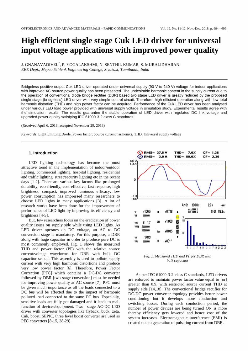
most commonly employed. Fig. 1 shows the measured
THD and power factor (PF) with the relative source
current/voltage waveforms for DBR with bulk DC
capacitor set up. This assembly is used to pollute supply
current with very high harmonic distortions and produce
very low power factor [6]. Therefore, Power Factor
Correction [PFC] which contains a DC-DC converter
followed by DBR [two-stage conversion] must be needed
for improving power quality at AC source [7]. PFC must
be given much importance as all the loads connected to a
DC bus will be affected due to the impact of harmonic
polluted load connected to the same DC bus. Especially,
sensitive loads are fully got damaged and it leads to mal-
function of devices/equipment. Two –stage AC-DC LED
driver with converter topologies like flyback, buck, zeta,
Cuk, boost, SEPIC, three level boost converter are used as
PFC converters [8-15, 28-29].
Fig. 1. Measured THD and PF for DBR with
bulk capacitor
As per IEC 61000-3-2 class C standards, LED drivers
are enforced to maintain power factor value equal to [or]
greater than 0.9, with restricted source current THD at
supply side [14,18]. The convectional bridge rectifier for
DC-DC power converter topology provides better power
conditioning but it develops more conduction and
switching losses. During each conduction period, the
number of power devices are being turned ON is more
thereby efficiency gets lowered and hence cost of the
system increases. Electromagnetic interference (EMI) is
created due to generation of pulsating current from DBR.

High efficient single stage Cuk LED driver for universal input voltage applications with improved power quality 695
In order to overcome these limitations, bridgeless
single stage PFC converter topologies have been emerged
[18-25]. As only half of the total current is being passed
through the devices, bridgeless converter circuit minimizes
the conduction loss to a greater extent. Also, when
operated in DCM, control circuit becomes much simpler
since there exists only mono voltage loop. Thus, reduction
in number sensing parameters leads to cost-effective
control circuit. Moreover, DCM provides way for
achieving inherent power factors naturally [18]. Bridgeless
boost PFC converters have been developed which can
operate either in CCM/DCM. But the major issues
regarding boost type PFC is i) high start-up/overload in
rush current ii) magnitude of output voltage is always
higher than provided supply voltage [21]. Bridgeless buck
type PFC converters have been preferred as in [22]. Highly
distorted and irregular shaping of line current are the
serious drawbacks regarding buck PFC converter. Here,
magnitude of output voltage obtained is always lesser than
that of applied input voltage [23]. Regarding buck boost
type converters, bridgeless, SEPIC and Cuk PFC
converters have been used.
Number of research works using bridgeless SEPIC
rectifier with improved efficiency as in [26-27] are
applicable for low to high power applications. Yet, the
usage of very large inductance for suppressing inductor
current ripple restricts the usage of bridgeless SEPIC in
many sensitive applications. Unlike these buck, boost and
SEPIC rectifiers, Cuk PFC converters possess several
merits like very less input/output current ripples, very
small EMI filter, capable of withstanding high start
UP/overloads in rush current. Moreover, it is easier to
implement isolation [21,23]. Generally, Cuk converter
produces negative output voltage.
This paper presents the novel bridgeless type single
switch Cuk PFC converter fed LED driver for
indoor/outdoor lighting operated under universal supply
voltage. The proposed LED driver needs no inverse
amplifier circuitry for generation of positive load voltage.
A very simplified control circuitry with PI voltage
controller is provided to regulate LED load voltage. In
addition, reduced supply current harmonic distortion [ less
than 5%] with unity power factor is achieved. Hence,
regulated DC voltage for LED driver along with better
input side power quality is achieved using this single stage
proposed LED driver.
2. Circuit description
The power circuit of proposed single switch Cuk LED
driver with the schematic block diagram of simple control
circuit is presented in Fig. 2. The control circuit needs only
single parameter sensing as the Cuk LED driver operates
in DCM. An analogy is made between the desired LED
driver voltage and the measured LED driver voltage. The
difference in voltage is processed by PI controller to
generate gate pulse for MOSFET with the help of ramp
signal. The desired switching frequency is achieved by
proper ramp signal generation. With this simple control
circuit, the satisfactory results of improved power quality
(Less THD, High Power Factor) are acquired in the input
side AC supply. Rated LED power is 100 W. Rated AC
supply voltage is 120 V.
Fig. 2. Proposed single switch Cuk LED driver with the schematic control block diagram
The upcoming section describes the three operating
modes of Cuk LED driver.
3. Operation modes
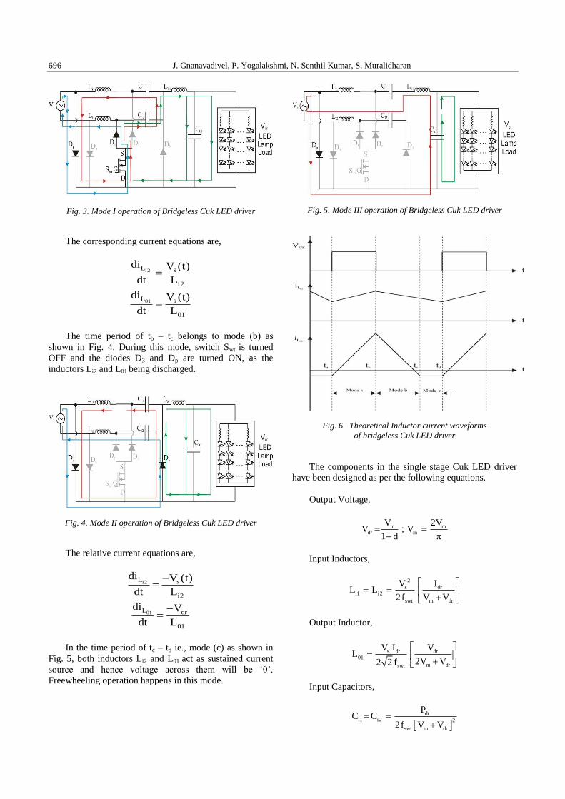
The time period of ta – tb (as seen in Fig. 6)
corresponds to mode (a) as shown in Fig. 3. During this
time period (ta – tb), the diode Dp gets forward biased and
the current flows through the switch Swt and charge the
inductors Li2 and L01 with diode D2 ON. Hence, voltage
across both input and output inductors will be equivalent
to AC supply voltage.
696 J. Gnanavadivel, P. Yogalakshmi, N. Senthil Kumar, S. Muralidharan
Fig. 3. Mode I operation of Bridgeless Cuk LED driver
The corresponding current equations are,
i2
01
L s
i2
L s
01
di V (t)
dt L
di V (t)
dt L
The time period of tb – tc belongs to mode (b) as
shown in Fig. 4. During this mode, switch Swt is turned
OFF and the diodes D3 and Dp are turned ON, as the
inductors Li2 and L01 being discharged.
Fig. 4. Mode II operation of Bridgeless Cuk LED driver
The relative current equations are,
i2
01
L s
i2
L dr
01
di V (t)
dt L
di V
dt L
In the time period of tc – td ie., mode (c) as shown in
Fig. 5, both inductors Li2 and L01 act as sustained current
source and hence voltage across them will be ‘0’.
Freewheeling operation happens in this mode.
Fig. 5. Mode III operation of Bridgeless Cuk LED driver
Fig. 6. Theoretical Inductor current waveforms
of bridgeless Cuk LED driver
The components in the single stage Cuk LED driver
have been designed as per the following equations.
Output Voltage,
in m
dr in
V 2VV ; V
1 d
Input Inductors,
2
s dr
i1 i2
swt m dr
V IL L
2f V V
Output Inductor,
s dr dr
01
m drswt
V .I VL
2V V2 2 f
Input Capacitors,
dr
i1 i2 2
swt m dr
PC C
2f V V
High efficient single stage Cuk LED driver for universal input voltage applications with improved power quality 697
Output Capacitor,
dr
01
dr
IC
2 V
where, Vs – AC supply voltage, Vm – Maximum value of
AC supply voltage, fswt – Switching frequency, Vdr – LED
driver voltage, Idr – LED driver current, Pdr – LED driver
power, d – duty cycle. The design values of above
mentioned components of LED driver are tabulated in
Table 1.
Table 1. Ratings of Cuk LED driver components
Cuk LED Driver components Ratings
Input inductors (Li1, Li2) 5 mH
Output inductor (L01) 50 µH
Input capacitors (Ci1, Ci2) 220 nF
Output capacitor (C01) 2200 µH
4. Simulation study and analysis of CUK LED driver
The performance of the proposed LED driver under
universal supply voltage are analysed in both simulation
and experimental study. Supply voltage/ current
waveforms at 120 Vrms voltage under rated LED driver
voltage along with the corresponding FFT analysis of
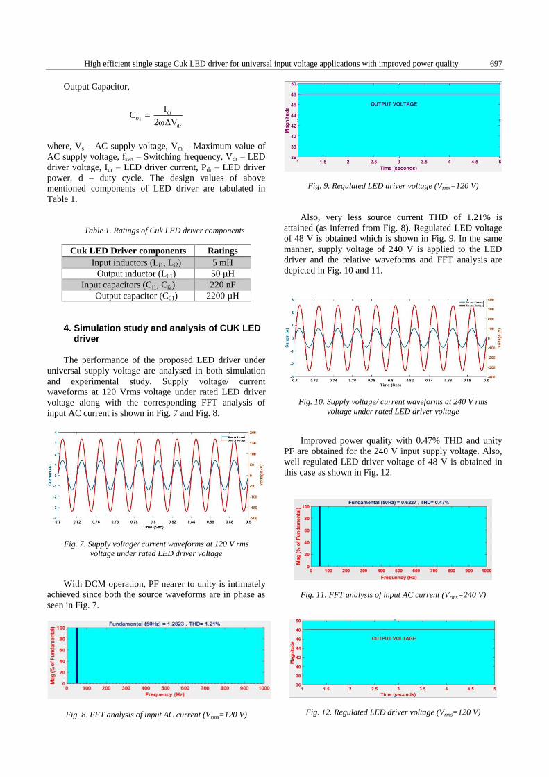
input AC current is shown in Fig. 7 and Fig. 8.
Fig. 7. Supply voltage/ current waveforms at 120 V rms
voltage under rated LED driver voltage
With DCM operation, PF nearer to unity is intimately
achieved since both the source waveforms are in phase as
seen in Fig. 7.
Fig. 8. FFT analysis of input AC current (Vrms=120 V)
Fig. 9. Regulated LED driver voltage (Vrms=120 V)
Also, very less source current THD of 1.21% is
attained (as inferred from Fig. 8). Regulated LED voltage
of 48 V is obtained which is shown in Fig. 9. In the same
manner, supply voltage of 240 V is applied to the LED
driver and the relative waveforms and FFT analysis are
depicted in Fig. 10 and 11.
Fig. 10. Supply voltage/ current waveforms at 240 V rms
voltage under rated LED driver voltage
Improved power quality with 0.47% THD and unity
PF are obtained for the 240 V input supply voltage. Also,
well regulated LED driver voltage of 48 V is obtained in
this case as shown in Fig. 12.
Fig. 11. FFT analysis of input AC current (Vrms=240 V)
Fig. 12. Regulated LED driver voltage (Vrms=120 V)
698 J. Gnanavadivel, P. Yogalakshmi, N. Senthil Kumar, S. Muralidharan
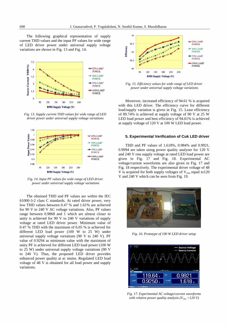
The following graphical representation of supply
current THD values and the input PF values for wide range
of LED driver power under universal supply voltage
variations are shown in Fig. 13 and Fig. 14.
Fig. 13. Supply current THD values for wide range of LED
driver power under universal supply voltage variations
Fig. 14. Input PF values for wide range of LED driver
power under universal supply voltage variations
The obtained THD and PF values are within the IEC
61000-3-2 class C standards. At rated driver power, very
low THD values between 0.47 % and 1.61% are achieved
for 90 V to 240 V AC voltage variations. Also, PF values
range between 0.9868 and 1 which are almost closer to
unity is achieved for 90 V to 240 V variations of supply
voltage at rated LED driver power. Minimum value of
0.47 % THD with the maximum of 6.05 % is achieved for
different LED load power (100 W to 25 W) under
universal supply voltage variations (90 V to 240 V). PF
value of 0.9294 as minimum value with the maximum of
unity PF is achieved for different LED load power (100 W
to 25 W) under universal supply voltage variations (90 V
to 240 V). Thus, the proposed LED driver provides
enhanced power quality at ac mains. Regulated LED load
voltage of 48 V is obtained for all load power and supply
variations.
Fig. 15. Efficiency values for wide range of LED driver
power under universal supply voltage variations
Moreover, increased efficiency of 94.61 % is acquired
with this LED driver. The efficiency curve for different
load/supply variation is given in Fig. 15. Least efficiency
of 89.74% is achieved at supply voltage of 90 V at 25 W
LED load power and best efficiency of 94.61% is achieved
at supply voltage of 120 V at 100 W LED load power.
5. Experimental Verification of Cuk LED driver THD and PF values of 1.618%, 0.984% and 0.9921,
0.9994 are taken using power quality analyser for 120 V
and 240 V rms supply voltage at rated LED load power are
given in Fig. 17 and Fig. 18. Experimental AC
voltage/current waveforms are also given in Fig. 17 and
Fig. 18 respectively. The experimental driver voltage of 48
V is acquired for both supply voltages of Vrms equal to120
V and 240 V which can be seen from Fig. 19.
Fig. 16. Prototype of 100 W LED driver setup
Fig. 17. Experimental AC voltage/current waveforms
with relative power quality analysis (Vrms =120 V)

High efficient single stage Cuk LED driver for universal input voltage applications with improved power quality 699
Fig. 18. Experimental AC voltage/current waveforms
with relative power quality analysis (Vrms =240 V)
Fig. 19. Experimental LED driver voltage waveform
(Vrms =120 V, 240 V)
6. Conclusions
A new bridgeless Cuk LED driver with simple closed
control for universal supply voltage applications has been
presented in this paper. Poor power quality at input AC
supply due to LED driver is eradicated by proper control
circuit. Evaluation of Cuk LED driver for universal input
voltage (90 V – 240 V) under wide LED load power has
been analysed. Reduced supply current THD of 0.47% and
unity PF along with 94.61% efficiency are attained using
this single stage Cuk LED driver. Component ratings are
reduced to half the value as compared to conventional two
stage PFC converter. Due to DCM operation,
conduction/switching losses are greatly reduced and hence
efficiency gets improved. Experimental set up is built and
the results are validated with the simulation one.
References
[1] Rero Marques Rubinger et al., Optical Engineering
54(1), 014104 (2015).
[2] Xuehui Tao, Bin Yang, Journal of Power Electronics
16(2), 815 (2016).
[3] D. G. Lamar, et. al., IEEE Transactions on Power
Electronics 24(8), 2032 (2009).
[4] Y. Chen, et al., IEEE Transactions on Power
Electronics 30(8), 4327 (2015).
[5] H. Ma, et al., IEEE Transactions on Power
Electronics 31(8), 5825 (2016).
[6] S. Singh, et al., IEEE Transactions on Industry
Applications 52(5), 4385 (2016).
[7] B. Singh, et al., IEEE Transactions on Industry
Applications 50(5), 962 (2003).
[8] J Gnanavadivel, et al., J. Optoelectron. Adv. M.
18(5-6), 459 (2016).
[9] J.-M. Kwon, et al., Proceeding of IEE Electric Power
Applications 153, 673 (2006).
[10] V. Bist, B. Singh, IEEE Transactions on Power
Electronics 30(2), 871 (2015).
[11] P. Shobana, et al., International Conference on
Computing, Electronics and Electrical Technologies
(ICCEET), 254-258 (2012).
[12] S. Singh, B. Singh, IEEE Transactions on Industry
Applications 48(2), 832 (2012).
[13] C. A. Cheng et al., LET Power Electronics 5(9), 1614
(2012).
[14] S. C. Moon, et al., IEEE Transactions on Power
Electronics 28(8), 4051 (2013).
[15] Chun-An Cheng, et al., Journal of Power Electronics
16(4), 1288 (2016).
[16] V. Chellappa, et al., Proceeding of International
Conference on Emerging Trends in Electrical and
Computer Technology, 430–435 (2011).
[17] Shikha Singh, et al., IET Power Electronics 9(8),
1684 (2016). [18] D. S. L. Simonetti, et al., IEEE Transactions on
Industrial Electronics 44(5), 630 (1997).
[19] Khairul Safuan Bin Muhammad, Dylan Dah-Chuan
Lu, IEEE Transactions on Industrial Electronics
62(5), 2795 (2015).
[20] Vashist Bist, Bhim Singh, IEEE Transactions on
Industrial Electronics 61(6), 2665 (2014).
[21] A. Abbas, et al., IEEE Transactions on Power
Electronics 27(7), 3292 (2012).
[22] Yungtaek Jang, Milan M. Jovanović, IEEE
Transactions on Power Electronics 26(2), 602 (2011).
[23] Ahmad J. Sabzali, et al., IEEE Transactions on
Industry Applications 47(2), 873 (2011).
[24] Laszlo Huber, et al., IEEE Transactions on Power
Electronics 23(3), 1381 (2008).
[25] Chun-An Cheng, et al., IEEE Transactions on Power
Electronics 30(2), 956 (2015).
[26] Mohammad Mahdavi, Hosein Farzanehfard, IEEE
Transactions on Industrial Electronics 58(9), 4153
(2011).
[27] Esam H. Ismail, IEEE Transactions on Industrial
Electronics 56(4), 1147 (2009).
[28] J. Gnanavadivel, N. Senthil Kumar, S. T. Jaya
Christa, Optoelectron. Adv. Mat. 9(9-10), 1264
(2015).
[29] J. Gnanavadivel, N. Senthil Kumar, P. Yogalakshmi,
Indian Journal of Geo Marine Sciences 46(9), 1908
(2017).
_______________________ *Corresponding author: [email protected],