Display LED Driver Reference Design - Texas Instruments
15
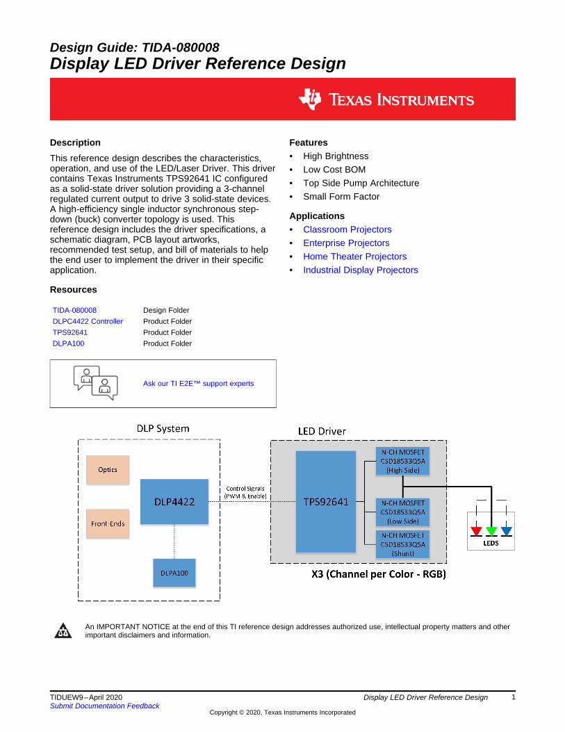
1 TIDUEW9 – April 2020 Submit Documentation Feedback Copyright © 2020, Texas Instruments Incorporated Display LED Driver Reference Design Design Guide: TIDA-080008 Display LED Driver Reference Design Description This reference design describes the characteristics, operation, and use of the LED/Laser Driver. This driver contains Texas Instruments TPS92641 IC configured as a solid-state driver solution providing a 3-channel regulated current output to drive 3 solid-state devices. A high-efficiency single inductor synchronous step- down (buck) converter topology is used. This reference design includes the driver specifications, a schematic diagram, PCB layout artworks, recommended test setup, and bill of materials to help the end user to implement the driver in their specific application. Resources TIDA-080008 Design Folder DLPC4422 Controller Product Folder TPS92641 Product Folder DLPA100 Product Folder Ask our TI E2E™ support experts Features • High Brightness • Low Cost BOM • Top Side Pump Architecture • Small Form Factor Applications • Classroom Projectors • Enterprise Projectors • Home Theater Projectors • Industrial Display Projectors An IMPORTANT NOTICE at the end of this TI reference design addresses authorized use, intellectual property matters and other important disclaimers and information.
-
Upload
khangminh22 -
Category
Documents
-
view
0 -
download
0
Transcript of Display LED Driver Reference Design - Texas Instruments
1TIDUEW9–April 2020Submit Documentation Feedback
Copyright © 2020, Texas Instruments Incorporated
Display LED Driver Reference Design
Design Guide: TIDA-080008Display LED Driver Reference Design
DescriptionThis reference design describes the characteristics,operation, and use of the LED/Laser Driver. This drivercontains Texas Instruments TPS92641 IC configuredas a solid-state driver solution providing a 3-channelregulated current output to drive 3 solid-state devices.A high-efficiency single inductor synchronous step-down (buck) converter topology is used. Thisreference design includes the driver specifications, aschematic diagram, PCB layout artworks,recommended test setup, and bill of materials to helpthe end user to implement the driver in their specificapplication.
Resources
TIDA-080008 Design FolderDLPC4422 Controller Product FolderTPS92641 Product FolderDLPA100 Product Folder
Ask our TI E2E™ support experts
Features• High Brightness• Low Cost BOM• Top Side Pump Architecture• Small Form Factor
Applications• Classroom Projectors• Enterprise Projectors• Home Theater Projectors• Industrial Display Projectors
An IMPORTANT NOTICE at the end of this TI reference design addresses authorized use, intellectual property matters and otherimportant disclaimers and information.
System Overview www.ti.com
2 TIDUEW9–April 2020Submit Documentation Feedback
Copyright © 2020, Texas Instruments Incorporated
Display LED Driver Reference Design
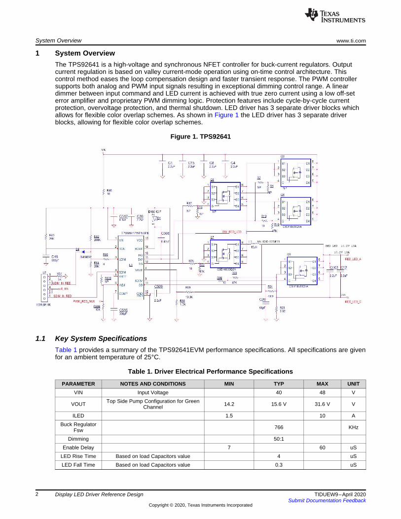
1 System OverviewThe TPS92641 is a high-voltage and synchronous NFET controller for buck-current regulators. Outputcurrent regulation is based on valley current-mode operation using on-time control architecture. Thiscontrol method eases the loop compensation design and faster transient response. The PWM controllersupports both analog and PWM input signals resulting in exceptional dimming control range. A lineardimmer between input command and LED current is achieved with true zero current using a low off-seterror amplifier and proprietary PWM dimming logic. Protection features include cycle-by-cycle currentprotection, overvoltage protection, and thermal shutdown. LED driver has 3 separate driver blocks whichallows for flexible color overlap schemes. As shown in Figure 1 the LED driver has 3 separate driverblocks, allowing for flexible color overlap schemes.
Figure 1. TPS92641
1.1 Key System SpecificationsTable 1 provides a summary of the TPS92641EVM performance specifications. All specifications are givenfor an ambient temperature of 25°C.
Table 1. Driver Electrical Performance Specifications
PARAMETER NOTES AND CONDITIONS MIN TYP MAX UNITVIN Input Voltage 40 48 V
VOUT Top Side Pump Configuration for GreenChannel 14.2 15.6 V 31.6 V V
ILED 1.5 10 ABuck Regulator
Fsw 766 KHz
Dimming 50:1Enable Delay 7 60 uS
LED Rise Time Based on load Capacitors value 4 uSLED Fall Time Based on load Capacitors value 0.3 uS
www.ti.com System Overview
3TIDUEW9–April 2020Submit Documentation Feedback
Copyright © 2020, Texas Instruments Incorporated
Display LED Driver Reference Design
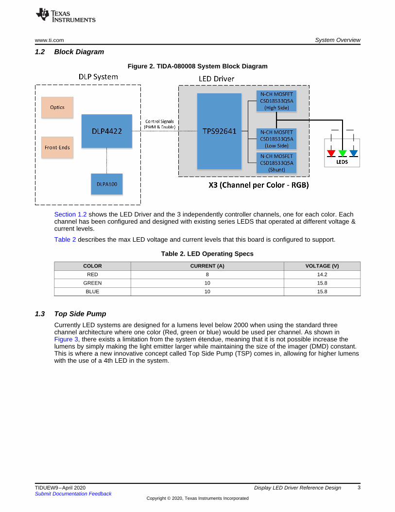
1.2 Block Diagram
Figure 2. TIDA-080008 System Block Diagram
Section 1.2 shows the LED Driver and the 3 independently controller channels, one for each color. Eachchannel has been configured and designed with existing series LEDS that operated at different voltage ¤t levels.
Table 2 describes the max LED voltage and current levels that this board is configured to support.
Table 2. LED Operating Specs
COLOR CURRENT (A) VOLTAGE (V)RED 8 14.2
GREEN 10 15.8BLUE 10 15.8
1.3 Top Side PumpCurrently LED systems are designed for a lumens level below 2000 when using the standard threechannel architecture where one color (Red, green or blue) would be used per channel. As shown inFigure 3, there exists a limitation from the system étendue, meaning that it is not possible increase thelumens by simply making the light emitter larger while maintaining the size of the imager (DMD) constant.This is where a new innovative concept called Top Side Pump (TSP) comes in, allowing for higher lumenswith the use of a 4th LED in the system.

System Overview www.ti.com
4 TIDUEW9–April 2020Submit Documentation Feedback
Copyright © 2020, Texas Instruments Incorporated
Display LED Driver Reference Design
Figure 3. Three Channel Configuration
To produce a green light, manufactures take a blue LED and use a green phosphor layer to convert theblue spectrum light into green. As shown in Figure 4, TSP takes advantage of this concept by adding anadditional blue LED to further excite the top side of the green phosphor to have a greater green output.The result is about an enhancement of 40%, but to maintain the white point, this translates toapproximately a 15% boost in lumens. The limiting factor for TSP is the red channel LED, if more red wasproduced, then more of the available green output could be used.
Figure 4. Top Side Pump Configuration
Green LED requires driving 2 diodes: Green LED and Blue pump LED together. With that in mind, hereare the real voltages that are supplied for the driver to accommodate Green and Blue pump LED nowrequires 31.6 V to driver both diodes in series.
Table 3. LED Operating Specs
COLOR CURRENT (A) VOLTAGE (V)Red 8 14.2
GREEN 10 31.6BLUE 10 15.8
www.ti.com System Overview
5TIDUEW9–April 2020Submit Documentation Feedback
Copyright © 2020, Texas Instruments Incorporated
Display LED Driver Reference Design
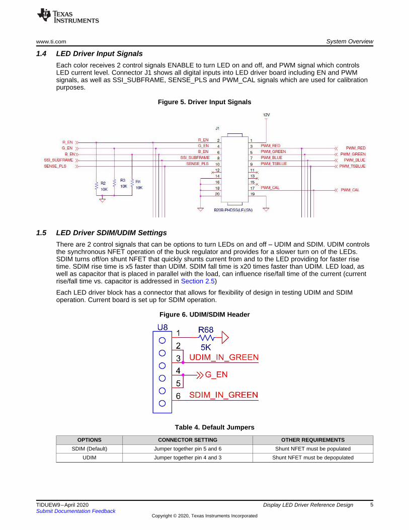
1.4 LED Driver Input SignalsEach color receives 2 control signals ENABLE to turn LED on and off, and PWM signal which controlsLED current level. Connector J1 shows all digital inputs into LED driver board including EN and PWMsignals, as well as SSI_SUBFRAME, SENSE_PLS and PWM_CAL signals which are used for calibrationpurposes.
Figure 5. Driver Input Signals
1.5 LED Driver SDIM/UDIM SettingsThere are 2 control signals that can be options to turn LEDs on and off – UDIM and SDIM. UDIM controlsthe synchronous NFET operation of the buck regulator and provides for a slower turn on of the LEDs.SDIM turns off/on shunt NFET that quickly shunts current from and to the LED providing for faster risetime. SDIM rise time is x5 faster than UDIM. SDIM fall time is x20 times faster than UDIM. LED load, aswell as capacitor that is placed in parallel with the load, can influence rise/fall time of the current (currentrise/fall time vs. capacitor is addressed in Section 2.5)
Each LED driver block has a connector that allows for flexibility of design in testing UDIM and SDIMoperation. Current board is set up for SDIM operation.
Figure 6. UDIM/SDIM Header
Table 4. Default Jumpers
OPTIONS CONNECTOR SETTING OTHER REQUIREMENTSSDIM (Default) Jumper together pin 5 and 6 Shunt NFET must be populated
UDIM Jumper together pin 4 and 3 Shunt NFET must be depopulated
CS
LED
CS
IADJ
CS
VI
R
VV
10
System Overview www.ti.com
6 TIDUEW9–April 2020Submit Documentation Feedback
Copyright © 2020, Texas Instruments Incorporated
Display LED Driver Reference Design
NOTE: Warning: Make sure UDIM is driven to 0 V during power up, especially when main supplythat drives LEDs is on. If UDIM is left floating, it will apply constant VLED voltage/current andmight damage the LED, if LED is meant to be pulsed.
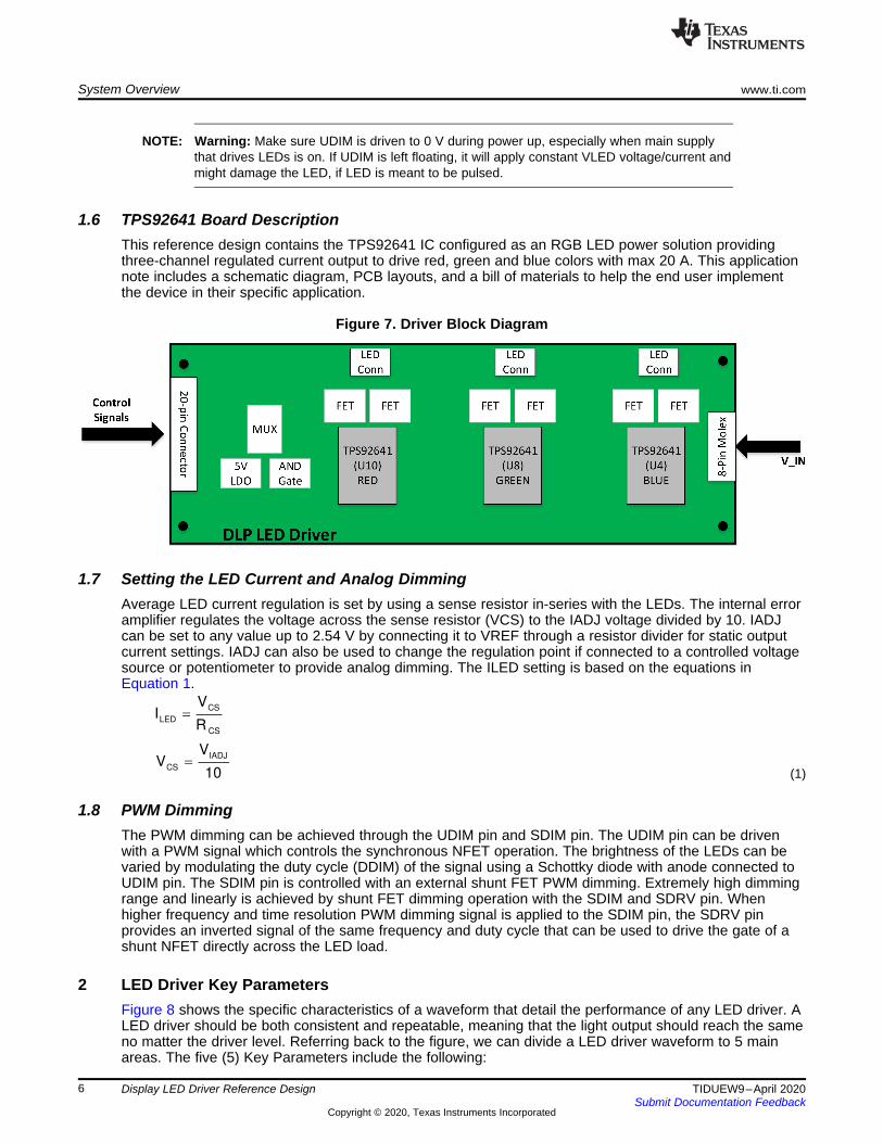
1.6 TPS92641 Board DescriptionThis reference design contains the TPS92641 IC configured as an RGB LED power solution providingthree-channel regulated current output to drive red, green and blue colors with max 20 A. This applicationnote includes a schematic diagram, PCB layouts, and a bill of materials to help the end user implementthe device in their specific application.
Figure 7. Driver Block Diagram
1.7 Setting the LED Current and Analog DimmingAverage LED current regulation is set by using a sense resistor in-series with the LEDs. The internal erroramplifier regulates the voltage across the sense resistor (VCS) to the IADJ voltage divided by 10. IADJcan be set to any value up to 2.54 V by connecting it to VREF through a resistor divider for static outputcurrent settings. IADJ can also be used to change the regulation point if connected to a controlled voltagesource or potentiometer to provide analog dimming. The ILED setting is based on the equations inEquation 1.
(1)
1.8 PWM DimmingThe PWM dimming can be achieved through the UDIM pin and SDIM pin. The UDIM pin can be drivenwith a PWM signal which controls the synchronous NFET operation. The brightness of the LEDs can bevaried by modulating the duty cycle (DDIM) of the signal using a Schottky diode with anode connected toUDIM pin. The SDIM pin is controlled with an external shunt FET PWM dimming. Extremely high dimmingrange and linearly is achieved by shunt FET dimming operation with the SDIM and SDRV pin. Whenhigher frequency and time resolution PWM dimming signal is applied to the SDIM pin, the SDRV pinprovides an inverted signal of the same frequency and duty cycle that can be used to drive the gate of ashunt NFET directly across the LED load.
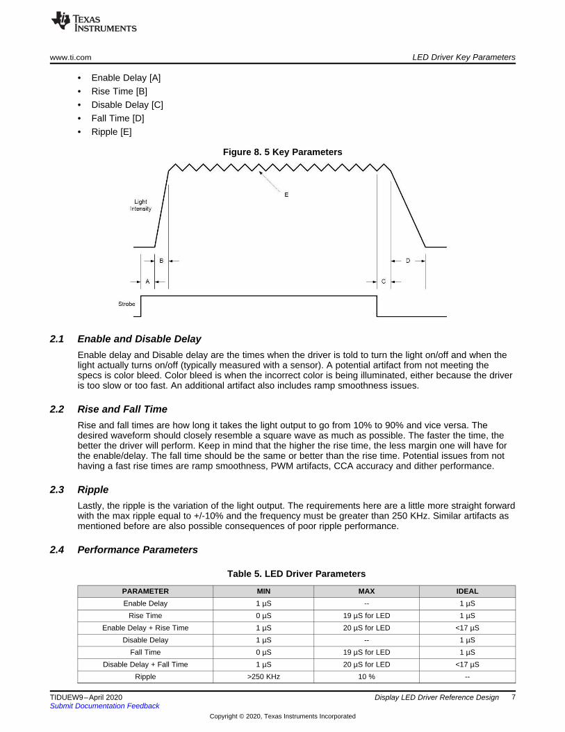
2 LED Driver Key ParametersFigure 8 shows the specific characteristics of a waveform that detail the performance of any LED driver. ALED driver should be both consistent and repeatable, meaning that the light output should reach the sameno matter the driver level. Referring back to the figure, we can divide a LED driver waveform to 5 mainareas. The five (5) Key Parameters include the following:
www.ti.com LED Driver Key Parameters
7TIDUEW9–April 2020Submit Documentation Feedback
Copyright © 2020, Texas Instruments Incorporated
Display LED Driver Reference Design
• Enable Delay [A]• Rise Time [B]• Disable Delay [C]• Fall Time [D]• Ripple [E]
Figure 8. 5 Key Parameters
2.1 Enable and Disable DelayEnable delay and Disable delay are the times when the driver is told to turn the light on/off and when thelight actually turns on/off (typically measured with a sensor). A potential artifact from not meeting thespecs is color bleed. Color bleed is when the incorrect color is being illuminated, either because the driveris too slow or too fast. An additional artifact also includes ramp smoothness issues.
2.2 Rise and Fall TimeRise and fall times are how long it takes the light output to go from 10% to 90% and vice versa. Thedesired waveform should closely resemble a square wave as much as possible. The faster the time, thebetter the driver will perform. Keep in mind that the higher the rise time, the less margin one will have forthe enable/delay. The fall time should be the same or better than the rise time. Potential issues from nothaving a fast rise times are ramp smoothness, PWM artifacts, CCA accuracy and dither performance.
2.3 RippleLastly, the ripple is the variation of the light output. The requirements here are a little more straight forwardwith the max ripple equal to +/-10% and the frequency must be greater than 250 KHz. Similar artifacts asmentioned before are also possible consequences of poor ripple performance.
2.4 Performance Parameters
Table 5. LED Driver Parameters
PARAMETER MIN MAX IDEALEnable Delay 1 µS -- 1 µS
Rise Time 0 µS 19 µS for LED 1 µSEnable Delay + Rise Time 1 µS 20 µS for LED <17 µS
Disable Delay 1 µS -- 1 µSFall Time 0 µS 19 µS for LED 1 µS
Disable Delay + Fall Time 1 µS 20 µS for LED <17 µSRipple >250 KHz 10 % --
LED Driver Key Parameters www.ti.com
8 TIDUEW9–April 2020Submit Documentation Feedback
Copyright © 2020, Texas Instruments Incorporated
Display LED Driver Reference Design
2.5 LED Load Capacitor for Rise/Fall TimeChoosing LED capacitor is very important when it comes to rise times, delay times, and current ripple.Here is a table what capacitor measurements that we made to help choose proper capacitor based on risetime and current ripple requirements. Capacitor choice might be different for Blue vs. Green LEDs. Greenand top side pump are placed in parallel and are a larger load to the driver compared to just a Blue LEDby itself.
Table 6. Load Capacitor effect on performance
COLOR CAP (UF)ENABLEDELAY
(US)RISE TIME (US) ENABLE DELAY + RISE
TIMERIPPLE PEAK TOPEAK (A)
Green 6.60 16.70 4.30 21.00 0.60Green 4.40 12.40 4.40 16.80 0.80Green 3.30 7.00 3.00 10.00 1.00Green 2.20 6.50 2.70 9.20 0.60Blue 10.0 11.20 3.60 14.80 0.64Blue 6.60 11.50 4.80 16.30 0.56Blue 4.40 8.70 3.40 12.10 0.72Blue 3.30 5.50 3.30 8.80 0.60Blue 2.20 4.00 1.90 5.90 0.56
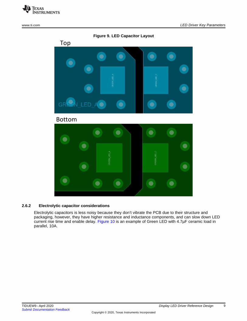
2.6 LED Load Capacitor And Audible NoiseCeramic capacitor are great when it comes to size and price, however, they can create audible noise inLED driver applications. As voltage across LED is turned on and off, capacitor flexes and vibrates thePCB, creating audible noise. There are two options to reducing this audible noise: layout considerations,as well as using an electrolytic capacitor.
2.6.1 Layout ConsiderationsThe two layout consideration options include:• Place two identical capacitors directly opposite each other on the top and bottom side of the PCB. If
there is only a single capacitor, it bends its middle towards the PCB and back. In doing this, the PCB isstimulated like the membrane of a loud speaker and emits acoustic waves. If two capacitors are placedopposite one another, both bend towards and away from the PCB at the same time. Thus, the PCBcannot resonate anymore.
• The second action to reduce the residual noise further is to minimize the mechanical coupling of theceramic capacitors and the PCB. By milling holes into the PCB besides the solder points, thestimulated PCB area is reduced significantly. Figure 4 shows the read marked holes in the PCB aroundthe ceramic capacitors Top view.
www.ti.com LED Driver Key Parameters
9TIDUEW9–April 2020Submit Documentation Feedback
Copyright © 2020, Texas Instruments Incorporated
Display LED Driver Reference Design
Figure 9. LED Capacitor Layout
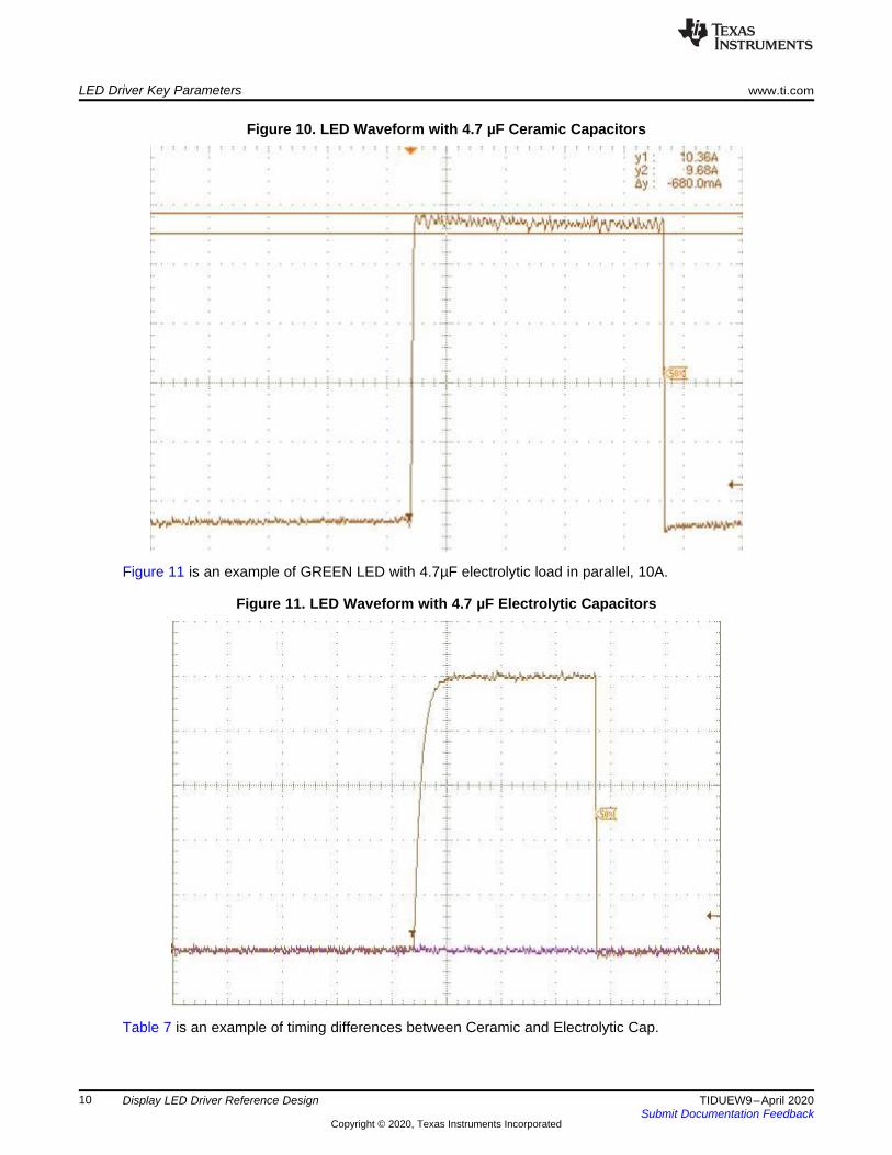
2.6.2 Electrolytic capacitor considerationsElectrolytic capacitors is less noisy because they don’t vibrate the PCB due to their structure andpackaging, however, they have higher resistance and inductance components, and can slow down LEDcurrent rise time and enable delay. Figure 10 is an example of Green LED with 4.7µF ceramic load inparallel, 10A.
LED Driver Key Parameters www.ti.com
10 TIDUEW9–April 2020Submit Documentation Feedback
Copyright © 2020, Texas Instruments Incorporated
Display LED Driver Reference Design
Figure 10. LED Waveform with 4.7 µF Ceramic Capacitors
Figure 11 is an example of GREEN LED with 4.7µF electrolytic load in parallel, 10A.
Figure 11. LED Waveform with 4.7 µF Electrolytic Capacitors
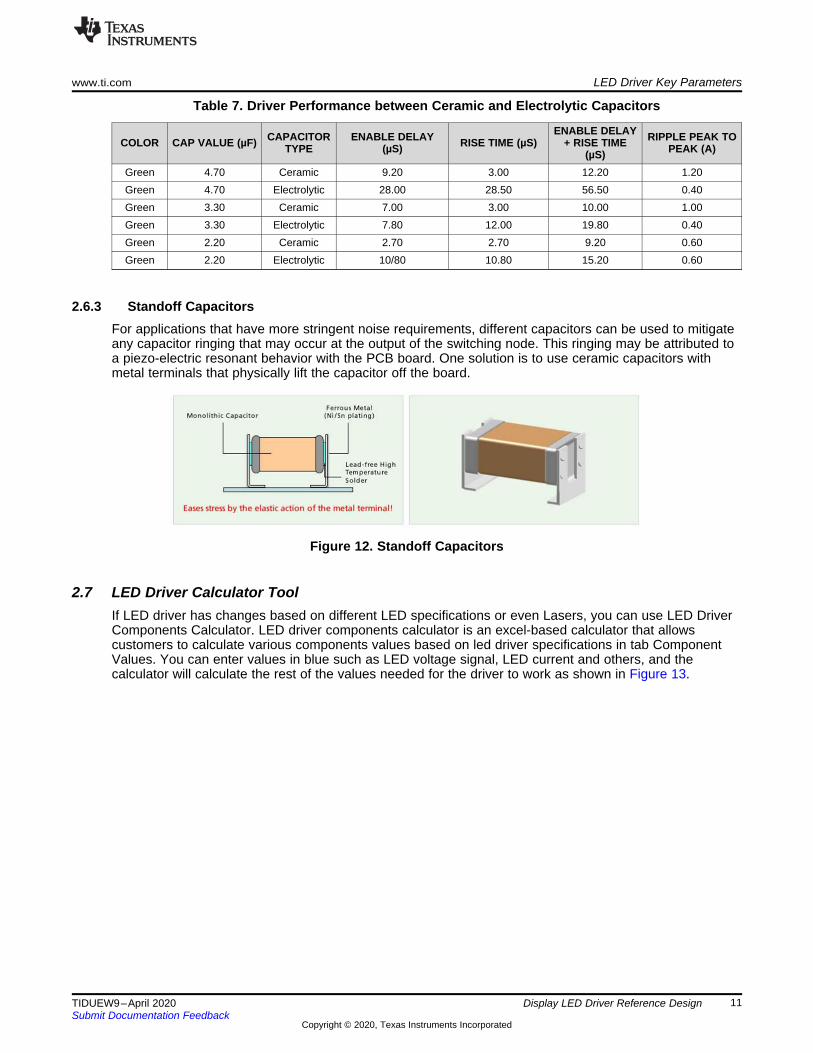
Table 7 is an example of timing differences between Ceramic and Electrolytic Cap.
www.ti.com LED Driver Key Parameters
11TIDUEW9–April 2020Submit Documentation Feedback
Copyright © 2020, Texas Instruments Incorporated
Display LED Driver Reference Design
Table 7. Driver Performance between Ceramic and Electrolytic Capacitors
COLOR CAP VALUE (µF) CAPACITORTYPE
ENABLE DELAY(µS) RISE TIME (µS)
ENABLE DELAY+ RISE TIME
(µS)RIPPLE PEAK TO
PEAK (A)
Green 4.70 Ceramic 9.20 3.00 12.20 1.20Green 4.70 Electrolytic 28.00 28.50 56.50 0.40Green 3.30 Ceramic 7.00 3.00 10.00 1.00Green 3.30 Electrolytic 7.80 12.00 19.80 0.40Green 2.20 Ceramic 2.70 2.70 9.20 0.60Green 2.20 Electrolytic 10/80 10.80 15.20 0.60
2.6.3 Standoff CapacitorsFor applications that have more stringent noise requirements, different capacitors can be used to mitigateany capacitor ringing that may occur at the output of the switching node. This ringing may be attributed toa piezo-electric resonant behavior with the PCB board. One solution is to use ceramic capacitors withmetal terminals that physically lift the capacitor off the board.
Figure 12. Standoff Capacitors
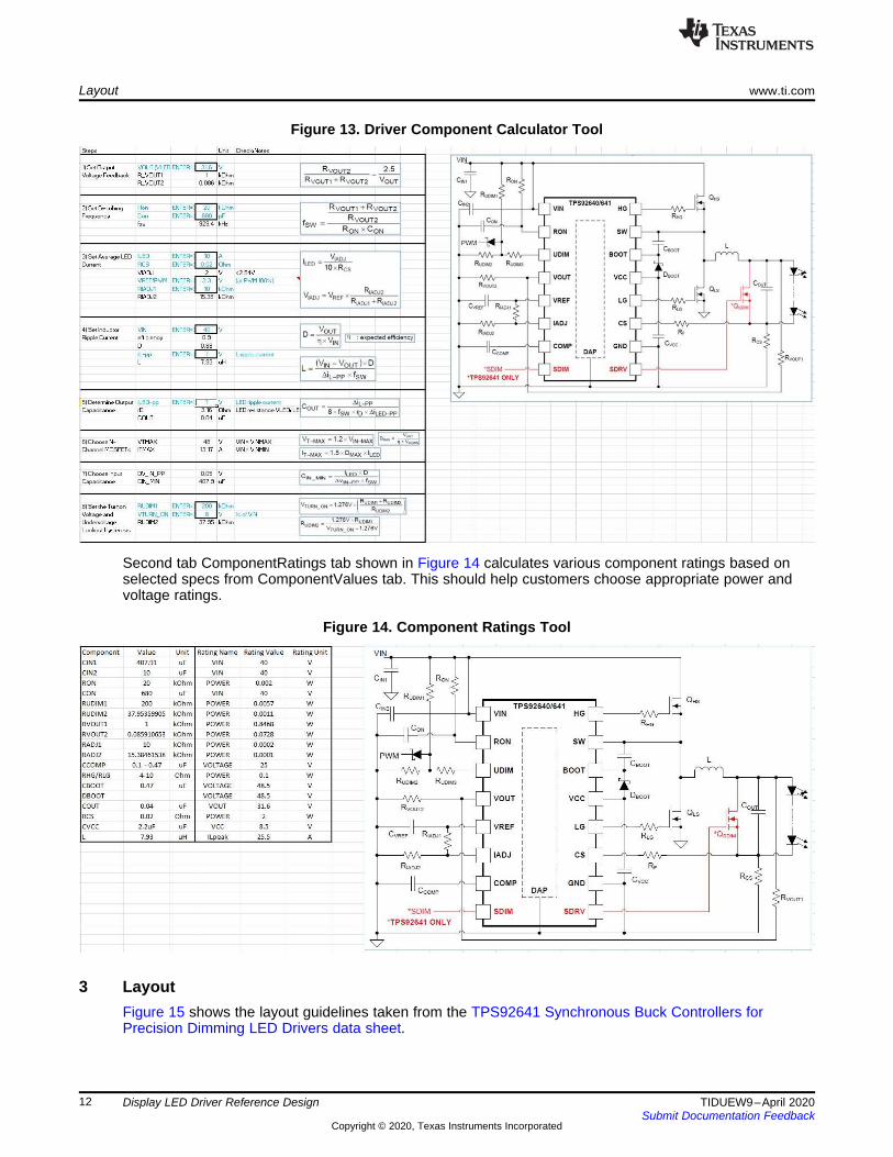
2.7 LED Driver Calculator ToolIf LED driver has changes based on different LED specifications or even Lasers, you can use LED DriverComponents Calculator. LED driver components calculator is an excel-based calculator that allowscustomers to calculate various components values based on led driver specifications in tab ComponentValues. You can enter values in blue such as LED voltage signal, LED current and others, and thecalculator will calculate the rest of the values needed for the driver to work as shown in Figure 13.
Layout www.ti.com
12 TIDUEW9–April 2020Submit Documentation Feedback
Copyright © 2020, Texas Instruments Incorporated
Display LED Driver Reference Design
Figure 13. Driver Component Calculator Tool
Second tab ComponentRatings tab shown in Figure 14 calculates various component ratings based onselected specs from ComponentValues tab. This should help customers choose appropriate power andvoltage ratings.
Figure 14. Component Ratings Tool
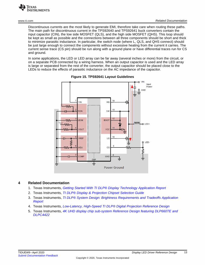
3 LayoutFigure 15 shows the layout guidelines taken from the TPS92641 Synchronous Buck Controllers forPrecision Dimming LED Drivers data sheet.
www.ti.com Related Documentation
13TIDUEW9–April 2020Submit Documentation Feedback
Copyright © 2020, Texas Instruments Incorporated
Display LED Driver Reference Design
Discontinuous currents are the most likely to generate EMI, therefore take care when routing these paths.The main path for discontinuous current in the TPS92640 and TPS92641 buck converters contain theinput capacitor (CIN), the low side MOSFET (QLS), and the high side MOSFET (QHS). This loop shouldbe kept as small as possible and the connections between all three components should be short and thickto minimize parasitic inductance. In particular, the switch node (where L, QLS, and QHS connect) shouldbe just large enough to connect the components without excessive heating from the current it carries. Thecurrent sense trace (CS pin) should be run along with a ground plane or have differential traces run for CSand ground.
In some applications, the LED or LED array can be far away (several inches or more) from the circuit, oron a separate PCB connected by a wiring harness. When an output capacitor is used and the LED arrayis large or separated from the rest of the converter, the output capacitor should be placed close to theLEDs to reduce the effects of parasitic inductance on the AC impedance of the capacitor.
Figure 15. TPS92641 Layout Guidelines
4 Related Documentation1. Texas Instruments, Getting Started With TI DLP® Display Technology Application Report2. Texas Instruments, TI DLP® Display & Projection Chipset Selection Guide3. Texas Instruments, TI DLP® System Design: Brightness Requirements and Tradeoffs Application
Report4. Texas Instruments, Low-Latency, High-Speed TI DLP® Digital Projection Reference Design5. Texas Instruments, 4K UHD display chip sub-system Reference Design featuring DLP660TE and
DLPC4422
Related Documentation www.ti.com
14 TIDUEW9–April 2020Submit Documentation Feedback
Copyright © 2020, Texas Instruments Incorporated
Display LED Driver Reference Design
4.1 TrademarksTI E2E is a trademark of Texas Instruments.All other trademarks are the property of their respective owners.
4.2 Third-Party Products DisclaimerTI'S PUBLICATION OF INFORMATION REGARDING THIRD-PARTY PRODUCTS OR SERVICES DOESNOT CONSTITUTE AN ENDORSEMENT REGARDING THE SUITABILITY OF SUCH PRODUCTS ORSERVICES OR A WARRANTY, REPRESENTATION OR ENDORSEMENT OF SUCH PRODUCTS ORSERVICES, EITHER ALONE OR IN COMBINATION WITH ANY TI PRODUCT OR SERVICE.

IMPORTANT NOTICE AND DISCLAIMERTI PROVIDES TECHNICAL AND RELIABILITY DATA (INCLUDING DATA SHEETS), DESIGN RESOURCES (INCLUDING REFERENCE DESIGNS), APPLICATION OR OTHER DESIGN ADVICE, WEB TOOLS, SAFETY INFORMATION, AND OTHER RESOURCES “AS IS” AND WITH ALL FAULTS, AND DISCLAIMS ALL WARRANTIES, EXPRESS AND IMPLIED, INCLUDING WITHOUT LIMITATION ANY IMPLIED WARRANTIES OF MERCHANTABILITY, FITNESS FOR A PARTICULAR PURPOSE OR NON-INFRINGEMENT OF THIRD PARTY INTELLECTUAL PROPERTY RIGHTS.These resources are intended for skilled developers designing with TI products. You are solely responsible for (1) selecting the appropriate TI products for your application, (2) designing, validating and testing your application, and (3) ensuring your application meets applicable standards, and any other safety, security, regulatory or other requirements.These resources are subject to change without notice. TI grants you permission to use these resources only for development of an application that uses the TI products described in the resource. Other reproduction and display of these resources is prohibited. No license is granted to any other TI intellectual property right or to any third party intellectual property right. TI disclaims responsibility for, and you will fully indemnify TI and its representatives against, any claims, damages, costs, losses, and liabilities arising out of your use of these resources.TI’s products are provided subject to TI’s Terms of Sale or other applicable terms available either on ti.com or provided in conjunction with such TI products. TI’s provision of these resources does not expand or otherwise alter TI’s applicable warranties or warranty disclaimers for TI products.TI objects to and rejects any additional or different terms you may have proposed. IMPORTANT NOTICE
Mailing Address: Texas Instruments, Post Office Box 655303, Dallas, Texas 75265Copyright © 2022, Texas Instruments Incorporated