Operational Transconductance Amplifier with Class B Slew ...
11
1 Operational Transconductance Amplifier with Class B Slew-Rate Boosting for Fast High-Performance Switched-Capacitor Circuits Mohammad H. Naderi, Student Member, IEEE, Suraj Prakash, Student Member, IEEE, Jose Silva-Martinez, Fellow, IEEE Abstract— In this paper, a technique for slew rate (SR) boosting suitable for switched-capacitor circuits is proposed. The proposed technique makes use of a class-B auxiliary amplifier that generates a compensating current only when high slew-rate is demanded by large signals. The proposed architecture employs simple circuitry to detect the need for a large output current by employing a highly sensitive pre-amplifier followed by a class- B amplifier. The functionality of the class-B transconductance amplifier is dictated by a predefined hysteresis, and operates in parallel with the main amplifier. The proposed solution demands small static power (under 20% of main amplifier power) due to its class-B nature. The experimental results in a 40 nm CMOS technology show more than 45% reduction in slew time, and a 28% shorter slew time for 1% settling time when used in a typical 4.5 bit/stage block commonly used in pipelined ADCs. Compared with the core amplifier, HD3 at 500 MHz reduces by more than 10dB when the slew-rate boosting circuit is activated. Index Terms— Slew rate boosting, switched-capacitor circuits, class B, linear settling, and high speed pipelined ADC. I. I NTRODUCTION M OST analog-to-digital converters (ADCs) like pipelined ADCs and discrete-time delta sigma modulators as well as high performance filters in the audio and video systems are based on switched-capacitor (SC) techniques [l]–[10]. For high-speed and large signal swing applications, the operational amplifier must settle into its final value within a time frame, which is a fraction of the main clock period, i.e., around 45% in the case of conventional two-phase SC circuits, which is usually in the range of nanoseconds for more than 100 MS/s (mega-samples per second) applications. For large signals, the settling process consists of two phases: slewing and linear settling. The slew phase does not require high precision, but a large amount of current is needed to more quickly move the output voltage from its initial condition closer to its final voltage value. Decreasing the slewing time allow us to allocate more time for the linear settling phase, which is dictated by loop bandwidth properties, e.g., gain-bandwidth products of the operational amplifier, loading conditions, feedback factor, and location of poles and zeros. The authors are with the Department of Electrical and Computer Engi- neering, Texas A&M University, College Station, TX 77843 USA (e-mail: [email protected]; [email protected]). Color versions of one or more of the figures in this paper are available online at http://ieeexplore.ieee.org. Usually, reducing the slewing time requires a large static current available at the amplifier’s output to efficiently drive the feedback and load networks. The high current requirement at the output stage of a class-A amplifier must satisfy the high slew-rate needs, which drastically increases the amplifier’s power consumption [11]–[15]. Current amplification has been used that is relying on increasing the tail-current efficiency by mirroring and amplifying the differential’s input stage current [16]–[23]. In SC circuits, the differential current is produced by a differential voltage step at the beginning of the settling phase that turns one of the differential input transistors OFF and another input transistor ON [24]–[26]; this is especially noticeable in the presence of large input steps. The differential current, which is dictated by the input stage tail current, is mirrored and amplified and then delivered to the loading impedance. As a result, a high slew-rate is achieved at the expense of higher power consumption. There are additional limitations in the case of low supply voltage deep sub-micron technologies. By reducing the full- scale voltage in pipeline ADCs, the voltage step across the differential input transistor is relatively small and may not exceed the input stage’s overdrive voltage. This effect is often present when large number of bits per stage are used; the input voltage is reduced to be the ADC’s full-scale value divided by 2 N ; N being the number of bits resolved in that stage. Thus, only a small portion of the tail current used in the amplifier’s input stage is processed, then resulting in slower settling time. Therefore, in order to maintain faster settling time, large amount of dc bias current is needed. Moreover, the extensive use of class-A circuits will limit solution’s power efficiency. The slew rate can be boosted by utilizing class-AB stages [27, 28]. In [28], a class-AB stage provides high dynamic current when demanded, but the bias current is relatively small. For switched-capacitor circuits, large current values can be generated by utilizing a class-AB stage; however, the quiescent current has to be maintained at level such that the required linear settling requirements are satisfied. Settling errors are dictated by small signal parameters such as overall transconductance gain, bandwidth and low-frequency loop gain. Enhancing the slew rate utilizing a hybrid dynamic amplifier was proposed in [24]. However, the hybrid amplifier requires optimization of its different building blocks for slew rate, phase margin, stability, and accuracy. Also, since the initial step voltage in the pipelined stages decreases when Digital Object Identifier: 10.1109/TCSI.2018.2852273 1558-0806 c 2018 IEEE. Personal use is permitted, but republication/redistribution requires IEEE permission. See http://www.ieee.org/publications standards/publications/rights/index.html for more information.
-
Upload
khangminh22 -
Category
Documents
-
view
0 -
download
0
Transcript of Operational Transconductance Amplifier with Class B Slew ...

1
Operational Transconductance Amplifier with Class
B Slew-Rate Boosting for Fast High-Performance
Switched-Capacitor CircuitsMohammad H. Naderi, Student Member, IEEE, Suraj Prakash, Student Member, IEEE,
Jose Silva-Martinez, Fellow, IEEE
Abstract— In this paper, a technique for slew rate (SR)boosting suitable for switched-capacitor circuits is proposed. Theproposed technique makes use of a class-B auxiliary amplifierthat generates a compensating current only when high slew-rateis demanded by large signals. The proposed architecture employssimple circuitry to detect the need for a large output current byemploying a highly sensitive pre-amplifier followed by a class-B amplifier. The functionality of the class-B transconductanceamplifier is dictated by a predefined hysteresis, and operates inparallel with the main amplifier. The proposed solution demandssmall static power (under 20% of main amplifier power) due toits class-B nature. The experimental results in a 40 nm CMOStechnology show more than 45% reduction in slew time, anda 28% shorter slew time for 1% settling time when used in atypical 4.5 bit/stage block commonly used in pipelined ADCs.Compared with the core amplifier, HD3 at 500 MHz reduces bymore than 10dB when the slew-rate boosting circuit is activated.
Index Terms— Slew rate boosting, switched-capacitor circuits,class B, linear settling, and high speed pipelined ADC.
I. INTRODUCTION
MOST analog-to-digital converters (ADCs) like pipelined
ADCs and discrete-time delta sigma modulators as well
as high performance filters in the audio and video systems
are based on switched-capacitor (SC) techniques [l]–[10]. For
high-speed and large signal swing applications, the operational
amplifier must settle into its final value within a time frame,
which is a fraction of the main clock period, i.e., around 45%
in the case of conventional two-phase SC circuits, which is
usually in the range of nanoseconds for more than 100 MS/s
(mega-samples per second) applications. For large signals, the
settling process consists of two phases: slewing and linear
settling. The slew phase does not require high precision, but
a large amount of current is needed to more quickly move
the output voltage from its initial condition closer to its final
voltage value. Decreasing the slewing time allow us to allocate
more time for the linear settling phase, which is dictated by
loop bandwidth properties, e.g., gain-bandwidth products of
the operational amplifier, loading conditions, feedback factor,
and location of poles and zeros.
The authors are with the Department of Electrical and Computer Engi-neering, Texas A&M University, College Station, TX 77843 USA (e-mail:[email protected]; [email protected]).
Color versions of one or more of the figures in this paper are availableonline at http://ieeexplore.ieee.org.
Usually, reducing the slewing time requires a large static
current available at the amplifier’s output to efficiently drive
the feedback and load networks. The high current requirement
at the output stage of a class-A amplifier must satisfy the high
slew-rate needs, which drastically increases the amplifier’s
power consumption [11]–[15]. Current amplification has been
used that is relying on increasing the tail-current efficiency by
mirroring and amplifying the differential’s input stage current
[16]–[23]. In SC circuits, the differential current is produced
by a differential voltage step at the beginning of the settling
phase that turns one of the differential input transistors OFF
and another input transistor ON [24]–[26]; this is especially
noticeable in the presence of large input steps. The differential
current, which is dictated by the input stage tail current,
is mirrored and amplified and then delivered to the loading
impedance. As a result, a high slew-rate is achieved at the
expense of higher power consumption.
There are additional limitations in the case of low supply
voltage deep sub-micron technologies. By reducing the full-
scale voltage in pipeline ADCs, the voltage step across the
differential input transistor is relatively small and may not
exceed the input stage’s overdrive voltage. This effect is often
present when large number of bits per stage are used; the input
voltage is reduced to be the ADC’s full-scale value divided
by 2N; N being the number of bits resolved in that stage.
Thus, only a small portion of the tail current used in the
amplifier’s input stage is processed, then resulting in slower
settling time. Therefore, in order to maintain faster settling
time, large amount of dc bias current is needed. Moreover,
the extensive use of class-A circuits will limit solution’s power
efficiency.
The slew rate can be boosted by utilizing class-AB stages
[27, 28]. In [28], a class-AB stage provides high dynamic
current when demanded, but the bias current is relatively
small. For switched-capacitor circuits, large current values
can be generated by utilizing a class-AB stage; however,
the quiescent current has to be maintained at level such
that the required linear settling requirements are satisfied.
Settling errors are dictated by small signal parameters such as
overall transconductance gain, bandwidth and low-frequency
loop gain. Enhancing the slew rate utilizing a hybrid dynamic
amplifier was proposed in [24]. However, the hybrid amplifier
requires optimization of its different building blocks for slew
rate, phase margin, stability, and accuracy. Also, since the
initial step voltage in the pipelined stages decreases when
Digital Object Identifier: 10.1109/TCSI.2018.2852273
1558-0806 c© 2018 IEEE. Personal use is permitted, but republication/redistribution requires IEEE permission.See http://www.ieee.org/publications standards/publications/rights/index.html for more information.
2
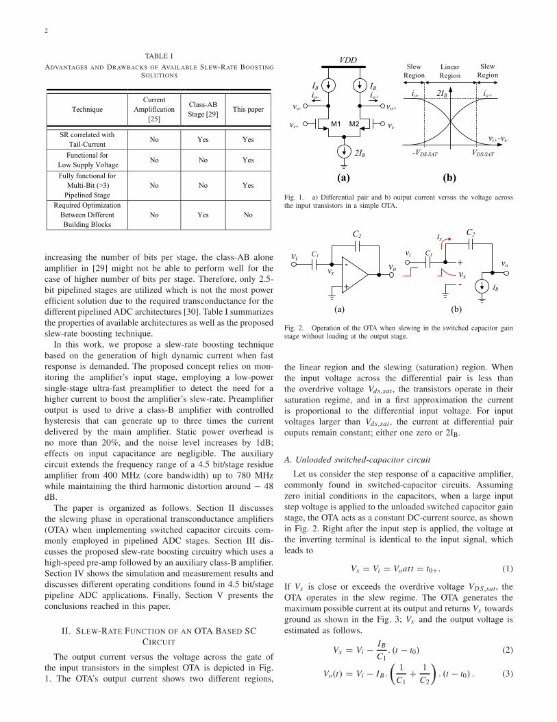
TABLE I
ADVANTAGES AND DRAWBACKS OF AVAILABLE SLEW-RATE BOOSTING
SOLUTIONS
increasing the number of bits per stage, the class-AB alone
amplifier in [29] might not be able to perform well for the
case of higher number of bits per stage. Therefore, only 2.5-
bit pipelined stages are utilized which is not the most power
efficient solution due to the required transconductance for the
different pipelined ADC architectures [30]. Table I summarizes
the properties of available architectures as well as the proposed
slew-rate boosting technique.
In this work, we propose a slew-rate boosting technique
based on the generation of high dynamic current when fast
response is demanded. The proposed concept relies on mon-
itoring the amplifier’s input stage, employing a low-power
single-stage ultra-fast preamplifier to detect the need for a
higher current to boost the amplifier’s slew-rate. Preamplifier
output is used to drive a class-B amplifier with controlled
hysteresis that can generate up to three times the current
delivered by the main amplifier. Static power overhead is
no more than 20%, and the noise level increases by 1dB;
effects on input capacitance are negligible. The auxiliary
circuit extends the frequency range of a 4.5 bit/stage residue
amplifier from 400 MHz (core bandwidth) up to 780 MHz
while maintaining the third harmonic distortion around − 48
dB.
The paper is organized as follows. Section II discusses
the slewing phase in operational transconductance amplifiers
(OTA) when implementing switched capacitor circuits com-
monly employed in pipelined ADC stages. Section III dis-
cusses the proposed slew-rate boosting circuitry which uses a
high-speed pre-amp followed by an auxiliary class-B amplifier.
Section IV shows the simulation and measurement results and
discusses different operating conditions found in 4.5 bit/stage
pipeline ADC applications. Finally, Section V presents the
conclusions reached in this paper.
II. SLEW-RATE FUNCTION OF AN OTA BASED SC
CIRCUIT
The output current versus the voltage across the gate of
the input transistors in the simplest OTA is depicted in Fig.
1. The OTA’s output current shows two different regions,
Fig. 1. a) Differential pair and b) output current versus the voltage acrossthe input transistors in a simple OTA.
Fig. 2. Operation of the OTA when slewing in the switched capacitor gainstage without loading at the output stage.
the linear region and the slewing (saturation) region. When
the input voltage across the differential pair is less than
the overdrive voltage Vds,sat , the transistors operate in their
saturation regime, and in a first approximation the current
is proportional to the differential input voltage. For input
voltages larger than Vds,sat , the current at differential pair
ouputs remain constant; either one zero or 2IB.
A. Unloaded switched-capacitor circuit
Let us consider the step response of a capacitive amplifier,
commonly found in switched-capacitor circuits. Assuming
zero initial conditions in the capacitors, when a large input
step voltage is applied to the unloaded switched capacitor gain
stage, the OTA acts as a constant DC-current source, as shown
in Fig. 2. Right after the input step is applied, the voltage at
the inverting terminal is identical to the input signal, which
leads to
Vx = Vi = Voatt = t0+. (1)
If Vx is close or exceeds the overdrive voltage VDS,sat, the
OTA operates in the slew regime. The OTA generates the
maximum possible current at its output and returns Vx towards
ground as shown in the Fig. 3; Vx and the output voltage is
estimated as follows.
Vx = Vi −IB
C1. (t − t0) (2)
Vo(t) = Vi − IB .
(
1
C1+
1
C2
)
. (t − t0) . (3)

3
Fig. 3. Operational transconductance amplifier (OTA) waveform input voltagewhen slewing in the switched capacitor gain stage without loading at theoutput stage.
The output slew rate is a function of the IB/C ratio and
its boosting requires larger amount of current and/or use of
smaller capacitors. Unfortunately, the capacitors cannot be
reduced since the thermal kT/C noise level must be maintained
at a low level; hence, a large amount of power is needed for
highly demanding systems that requires fast response and high
resolution.
In most practical cases, the capacitors are pre-charged from
a previous phase. In the worst case, the voltage variation at
the amplifier’s input would be even larger than expected. Right
after the circuit is reconfigured as shown in Fig. 2 based on
the capacitor’s initial conditions, the amplifier’s input voltage
is estimated after the capacitors are rearranged. This process
can be shown through the following equation and is obtained
using charge recombination techniques.
Vx(t0+) =C1 (Vi (t0+)−Vc1 (t0)) −C2Vc2 (t0)
C1 + C2. (4)
Vc1 (t0) and Vc2 (t0) in (4) correspond to the initial conditions
in C1 and C2, respectively. Equation (4) shows that the initial
voltage variation at the inverting terminal of the amplifier,
Vx (t0+), occurs after the connection of the capacitors. Accord-
ing to this equation, large excursions at the amplifier’s input
will occur when Vc1,2 (t0) and the input voltage Vi (t0+) have
opposite polarity; this is the worst case for a slew-rate and
slew may occur even if Vi (t0+) does not exceed Vds,sat .
The initial amplifier’s input voltage Vx(t0+) after the input
pulse is applied is returned to its steady state value according
to the slope of IB/C1 over time, as illustrated in Fig. 3.
This constant current condition is maintained until the voltage
across the input differential pair reaches the overdrive voltage;
then, the amplifier’s input stage will operate in a linear regime.
B. Loaded switched-capacitor circuit
Fig. 4 shows the operation of the amplifier slewing when
loaded by CL; the parasitic capacitor CP present at amplifier
input is also included. The output capacitor CL is usually pre-
charged to a voltage before the charge recombination phase;
this charge is a function of the operation of the following
stage during the previous clock phase. The initial charge stored
Fig. 4. OTA operation o when slewing in the switched capacitor gain stageby considering the load capacitor.
Fig. 5. Different slewing-time of the class-A residue amplifier based onthe initial stored-voltage on the load capacitor: a) differential amplifier inputvoltage Vx and b) amplifier’s output voltage. The 0.25% settling time for eachcase is 0.8 nsecs, 1.25 nsecs and 1.75 nsecs, respectively.
in all capacitors determines the instantaneous voltage at the
amplifier’s input after the capacitors are reconnected; Vx is
then computed as
Vx (t0+) =C1 (Vi (t0+) − Vc1 (t0)) − CP VC P (t0)
C1 + CP +C2CL
C2+C L
+
(
C2CL
C2+C L
)
(VC L (t0) − Vc2 (t0))
C1 + CP +C2CL
C2+C L
. (5)
In (5), VC L (t0) represents the initial voltage at CL, and
Vi (t0+) corresponds to the input voltage right after the input

4
Fig. 6. Simplified schematic of the proposed amplifier aided with an axillarypre-amp followed by a class-B amplifier to boost its overall slew rate.
Fig. 7. The low-power, high-performance pseudo class-AB architectureutilized as the main amplifier in the proposed topology in the multi-bit/stagepipelined ADC.
pulse is applied. Usually VC P (t0) is small compared with
the other terms and can be safely ignored for a sake of
simplification in the analysis. It is worth mentioning that the
amount of current that discharges Vx(t0+) is smaller than the
maximum amplifier output current, IB , since there is a current
divider effect due to the presence of CL . The amplifier’s input
voltage Vx (t) returns to its steady state according to:
Vx (t) = Vx (t0) −
⎛
⎝
IB
1 + CL
(
1C2
+ 1C1+CP
)
⎞
⎠
.
(
t − t0
C1 + CP
)
i f |Vx (t)| ≥Vdssat . (6)
The rate of variation of amplifier’s input voltage Vx is then
dictated by
S RV x = −
⎛
⎝
IB
1 + CL
(
1C2
+ 1C1+CP
)
⎞
⎠ .
(
1
C1 + CP
)
. (7)
Equation (7) shows the (dis)charging feedback current is a
portion of the maximum output current IB . The slew-rate is
determined by the current divider gain between CL and the
series of C2 and the parallel of C1 and Cp; the portion of the
current flowing through C2 is then integrated by C1 + Cp and
determines the speed of the variation at node Vx . The larger
the load capacitor CL is, the smaller the slew-rate. In a first
approximation, the slew time is then computed as follows:
Tslew =(
Vx (t0+) − Vds_sat
)
·
⎛
⎝
C1 + CP + CL
(
1 +C1+CP
C2
)
IB
⎞
⎠. (8)
According to (5) and (8), slew time is a function of the
capacitor’s initial conditions as well as the amplitude of the
input signal. The slew-time increases with large capacitors CL,
C1 and CP; it also increases when reducing C2.
To get more insight on the design trade-offs, let us consider
the case of a residue amplifier used in a 4.5-bit pipelined stage.
For this case, assume that the feedback factor β =C2
C1+C2=
1/16, amplifier’s gain-bandwidth product G BW = 4.5 G H z,
C1 = 825 f F , C2 = 55 f F , CL = 420 f F , Amplifier
DCGain = 43 d B , and sampling frequency Fs = 400 M H z.
The C1 and C2 values were based on the maximum total
allowed input referred noise limit to satisfy the thermal noise
requirement for the first 4.5-bit pipelined stage in a 12-bit
pipelined ADC. The CL value was based on minimum unit
capacitance for satisfying the mismatch requirement, input
referred noise, and considering 100 f F parasitic capacitance
from sub-ADC in the second 4.5-bit pipelined stage of a 12-bit
pipelined ADC. The target is to achieve a settling error under
0.25% in Ts/2 secs (1.25 nsecs). Fig. 5 displays the amplifier’s
transient response for three different initial conditions on the
load capacitor. According to these results, it is evident that
we have to consider the very worst case when computing
the required settling time. The 0.25% settling time for each
one of these cases is 0.8 nsecs, 1.25 nsecs and 1.75 nsecs,
respectively. The worst-case condition takes more than twice
the settling time of the best case.
According to equation (8), the slew time can be reduced by
increasing Vds_sat ; this approach, however, is not advisable
since linear settling time will be affected and limitation on
voltage headroom. Although the quadratic equation is not
accurate for short channel devices, it can help us to get
some intuition on the amplifier’s design tradeoffs; the tran-
sistor’s small signal transconductance of a differential pair is
approximated as gm ≈ 2IB/Vds_sat. The larger the saturation
voltage, the smaller the transconductance. On the other hand,
decreasing further the overdrive voltage of the differential pair
has a negative impact on the slew time the since transistor
may enter into a subthreshold region, thereby reducing its
current driving capability. Optimizing Vds_sat is recommended
for best bandwidth and required noise level; usually, a good
compromise is to keep its value in a range between 80 mV and
200 mV for the TSMC 40nm technology under 1.1V supply
voltage. The proposed design strategy is to make the design
procedure independent for the best possible slew rate and faster
linear settling.
5
TABLE II
AMPLIFIER DEVICE SIZES
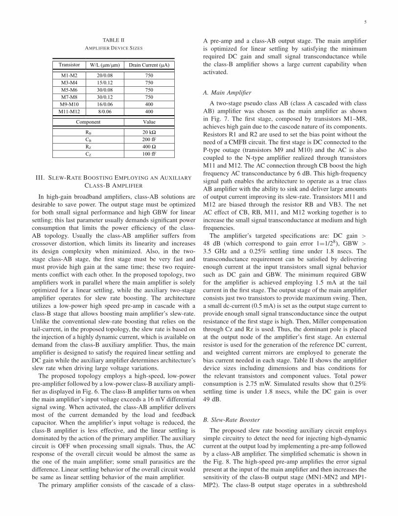
III. SLEW-RATE BOOSTING EMPLOYING AN AUXILIARY
CLASS-B AMPLIFIER
In high-gain broadband amplifiers, class-AB solutions are
desirable to save power. The output stage must be optimized
for both small signal performance and high GBW for linear
settling; this last parameter usually demands significant power
consumption that limits the power efficiency of the class-
AB topology. Usually the class-AB amplifier suffers from
crossover distortion, which limits its linearity and increases
its design complexity when minimized. Also, in the two-
stage class-AB stage, the first stage must be very fast and
must provide high gain at the same time; these two require-
ments conflict with each other. In the proposed topology, two
amplifiers work in parallel where the main amplifier is solely
optimized for a linear settling, while the auxiliary two-stage
amplifier operates for slew rate boosting. The architecture
utilizes a low-power high speed pre-amp in cascade with a
class-B stage that allows boosting main amplifier’s slew-rate.
Unlike the conventional slew-rate boosting that relies on the
tail-current, in the proposed topology, the slew rate is based on
the injection of a highly dynamic current, which is available on
demand from the class-B auxiliary amplifier. Thus, the main
amplifier is designed to satisfy the required linear settling and
DC gain while the auxiliary amplifier determines architecture’s
slew rate when driving large voltage variations.
The proposed topology employs a high-speed, low-power
pre-amplifier followed by a low-power class-B auxiliary ampli-
fier as displayed in Fig. 6. The class-B amplifier turns on when
the main amplifier’s input voltage exceeds a 16 mV differential
signal swing. When activated, the class-AB amplifier delivers
most of the current demanded by the load and feedback
capacitor. When the amplifier’s input voltage is reduced, the
class-B amplifier is less effective, and the linear settling is
dominated by the action of the primary amplifier. The auxiliary
circuit is OFF when processing small signals. Thus, the AC
response of the overall circuit would be almost the same as
the one of the main amplifier; some small parasitics are the
difference. Linear settling behavior of the overall circuit would
be same as linear settling behavior of the main amplifier.
The primary amplifier consists of the cascade of a class-
A pre-amp and a class-AB output stage. The main amplifier
is optimized for linear settling by satisfying the minimum
required DC gain and small signal transconductance while
the class-B amplifier shows a large current capability when
activated.
A. Main Amplifier
A two-stage pseudo class AB (class A cascaded with class
AB) amplifier was chosen as the main amplifier as shown
in Fig. 7. The first stage, composed by transistors M1–M8,
achieves high gain due to the cascode nature of its components.
Resistors R1 and R2 are used to set the bias point without the
need of a CMFB circuit. The first stage is DC connected to the
P-type outage (transistors M9 and M10) and the AC is also
coupled to the N-type amplifier realized through transistors
M11 and M12. The AC connection through CB boost the high
frequency AC transconductance by 6 dB. This high-frequency
signal path enables the architecture to operate as a true class
AB amplifier with the ability to sink and deliver large amounts
of output current improving its slew-rate. Transistors M11 and
M12 are biased through the resistor RB and VB3. The net
AC effect of CB, RB, M11, and M12 working together is to
increase the small signal transconductance at medium and high
frequencies.
The amplifier’s targeted specifications are: DC gain >
48 dB (which correspond to gain error 1=1/28), GBW >
3.5 GHz and a 0.25% settling time under 1.8 nsecs. The
transconductance requirement can be satisfied by delivering
enough current at the input transistors small signal behavior
such as DC gain and GBW. The minimum required GBW
for the amplifier is achieved employing 1.5 mA at the tail
current in the first stage. The output stage of the main amplifier
consists just two transistors to provide maximum swing. Then,
a small dc-current (0.5 mA) is set as the output stage current to
provide enough small signal transconductance since the output
resistance of the first stage is high. Then, Miller compensation
through Cz and Rz is used. Thus, the dominant pole is placed
at the output node of the amplifier’s first stage. An external
resistor is used for the generation of the reference DC current,
and weighted current mirrors are employed to generate the
bias current needed in each stage. Table II shows the amplifier
device sizes including dimensions and bias conditions for
the relevant transistors and component values. Total power
consumption is 2.75 mW. Simulated results show that 0.25%
settling time is under 1.8 nsecs, while the DC gain is over
49 dB.
B. Slew-Rate Booster
The proposed slew rate boosting auxiliary circuit employs
simple circuitry to detect the need for injecting high-dynamic
current at the output load by implementing a pre-amp followed
by a class-AB amplifier. The simplified schematic is shown in
the Fig. 8. The high-speed pre-amp amplifies the error signal
present at the input of the main amplifier and then increases the
sensitivity of the class-B output stage (MN1-MN2 and MP1-
MP2). The class-B output stage operates in a subthreshold

6
Fig. 8. The proposed auxiliary circuit for boosting main amplifier’s slewrate.
Fig. 9. Small-signal model of the pre-amplifier and coupling networkincluding CB and RB.
Fig. 10. Impulse response of a 2nd order amplifier (eqn. 11) showing theactivation voltage for the amplifier’s second stage (dashed line).
TABLE III
SLEW-RATE BOOSTER DEVICE SIZES
region to reduce power consumption; it also enables slew-
rate booster circuit operation with a defined hysteresis around
Fig. 11. Main amplifier’s (solid line) and the main amplifier’s with SRboosting (dotted line) frequency response: a) magnitude and b) phase.
16 mV. For that purpose, VBN and VBP voltages are properly
set. The transistors are computed such that MP1, MP2, MN1,
and MN2, can provide up to five times of the main amplifier
output current in the slew mode and in the presence of large
signals. Although the disadvantage of the class-B amplifiers
is the cross-over distortion, our proposed technique does not
suffer from this effect because the proposed class-B amplifier
is activated if and only if the signal swing at the input of
the main amplifier exceeds 16 mV, and that happen when the
signal is large; this stage remains OFF during small signal
operation.
The tail current of the pre-amp in the slew-rate booster is
0.4 mA; this current is smaller than the 1.5 mA tail current
of the main amplifier’s first stage. The in-band gain of the
front-end amplifier is 8 V/V, and the − 3dB bandwidth is as
high as 1 GHz. Also, the input capacitance of the pre-amp
is around 15 fF, which is small compared to the 65 fF of
the input capacitance of the main amplifier. This additional
capacitance does not have a major effect on either the loop
gain or the amplifier’s settling time. Table III displays the
device sizes including dimensions and bias conditions for
the relevant transistors and component values. The overhead
power consumption is 0.55 mW after utilizing this auxiliary
circuit, which is only 20% of the main amplifier power
consumption.
The small signal model of the preamplifier and coupling
network to the class-B output stage (see Fig. 8) used in the
proposed slew-rate booster circuit is shown in the Fig. 9. The
transfer function would be derived as
H (s) = gm1 ×R1 RBCBs
[(R1 RBCp1Cp2 + R1 RBCB(Cp1 + Cp2))]s2
+[R1Cp1+RBCp2 + (R1 + RB)CB ]s + 1
.(9)
In (9), Cp1 and Cp2 are the parasitic capacitances at the drain
of the M1 and gate of the MP1/MN1, respectively. Since the

7
parasitic capacitances are much smaller than CB , equation (9)
can be simplified as
H (s) =gm1 R1 RBCBs
(1 + sωP1
)(1 + sωP2
)(10)
where ωP1∼=
1RBCB
and ωP2∼=
1R1(C p1+C p2)
. The dominant
pole ωp1 is placed at low frequency, while the non-dominant
pole ωP2 is placed at the highest possible frequency. At
intermediate frequencies, the voltage gain is flat and dominated
by gm1 R1 if RB≫ R1. Although the small signal analysis is
interesting, it is not very useful since this circuit is not active
for small signals. More interesting is the large signal analysis
of its impulse and pulse response.
It can be shown that when enabled, the unity impulse
response of the 2nd order function represented by (10), follows
the behavior determined by
vo1 (t) ∼= (vo1|t=0)
(
e−ωP2t −
(
ωP1
ωP2
)
e−ωP1t
)
(11)
Significant slow components may result from this circuit
unless ωP2 ≫ ωP1. For this case, ωP1 is set at 100 Mrad/sec
while ωP2 is set around 6 Grad/sec. Thus, the peak value of
the slow component is 60 times smaller than the component
lumped to the fast exponential component in equation (11).
This equation is plot in Fig. 10; the dash line shows the
activation voltage set at 100 mV for the class B (second-
stage) amplifier, which correspond to a threshold voltage of
around 16 mV at first amplifier input. The first part of the
transient is dominated by the term e−ωP2 t ; after 1% settling
time, the behavior is dominated by the slow component e−ωP1t .
Notice in this figure that the slow settling component does not
play a major role on the operation of the class-B amplifier;
even 10% settling is enough for the proper functionality of
the architecture. The speed of the overall circuit is dominated
by the fast exponential component. Fig. 11 shows the main
amplifier’s frequency response versus the main amplifier with
SR boosting frequency response. Since the auxiliary circuit is
OFF when processing small signals, the AC response of the
overall circuit would be almost the same as the one of the
main amplifier; some small parasitics are the difference.
Fig. 12 shows the differential output current (from Cadence)
versus the input voltage for both the main amplifier and the
auxiliary amplifier. The auxiliary amplifier is turned OFF
when the main amplifier’s input voltage is less than 16 mV.
For small signal variations, the slew phase is not critical;
hence, the final settling time is determined by the parameters
of the main amplifier. When the input step voltage exceeds
the threshold voltage, the auxiliary amplifier delivers a high
dynamic current—more than triple of main amplifier’s output
current and over 10 times greater than class-B amplifier bias
current.
To compare the current capability of the current booster, a
differential narrow input pulse with 1 nsec width and 60 mV
amplitude was used. For this simulation, amplifier’s output was
connected to a small resistor to measure the time delay and
amount of current delivered by the amplifier components. Fig.
13 shows the results. The auxiliary class-B amplifier takes
less 300 psecs delay to deliver/sink more than 1.7 mA and
Fig. 12. Differential output current versus the input voltage for both themain amplifier (dotted line) and the auxiliary amplifier (solid line); cadenceresults.
Fig. 13. Pulse response current of the main amplifier (dotted line) and slew-rate booster circuit (solid line): output current.
Fig. 14. Differential output current for the standalone amplifier (dotted line)and for the main amplifier with auxiliary amplifier enabled (solid line).
takes around 700 psecs for 1% settling; main amplifier delivers
around 0.7 mA and settles (1%) in around 1500 psecs.
To verify the circuit behavior under a practical case, a 4.5-bit

8
Fig. 15. Chip micrograph.
Fig. 16. Simplified (single-ended) version of the amplifier characterizationsetup used to measure the performance of the slew-rate boosting technique.
Fig. 17. Measurement results of a large input step voltage for the pseudoclass-AB amplifier with SR boosted technique and the conventional pseudoclass-AB amplifier in the prototype of a 4.5-bit/stage pipelined ADC.
stage used in pipelined ADCs was used as a testbed; the very
small feedback factor β = 1/16 [30]. The input capacitance
(C1 = 16C2 in Fig. 6) was set at 880 fF while the feedback
capacitor was set at C2 = 55 fF; capacitive amplification
factor is 16. The capacitors were fully discharged, and the
input signal was pulsed from zero to 62.5 mV. Fig. 14 shows
the differential output current when the auxiliary amplifier
is enabled and for the case of the standalone amplifier.
The peak current of the enhanced architecture surpasses the
one of the conventional one by a factor of 240%. For the
proposed architecture, the current’s peak value is reached in
180 psecs compared to 380 psecs when the main amplifier was
operating alone. The superior performance of the proposed
amplifier is more evident if we consider the slew time for
the capacitive amplifier: 400 psecs for the proposed amplifier
with slew boosting technique vs. 1050 psecs required for the
conventional architecture.
IV. EXPERIMENTAL RESULTS
The amplifier along with the slew-rate boosting auxiliary
circuit was fabricated in the TSMC 40 nm CMOS process
using core devices with a nominal value of 1.1 V. Fig. 15
shows the die photo of the amplifier along with the slew-
rate boosting auxiliary circuit, where the core occupies 0.05
mm2. The single-ended test setup used to characterize the
performance of the amplifiers in the 4.5-bit/stage pipelined
stage prototype is shown in Fig. 16. The actual chip is fully
differential. An Agilent E8267D PSG vector signal generator
was used to supply the input signal and the output was cap-
tured using the Agilent Infiniium DSA91304A oscilloscope.
To preserve the high output impedance of the amplifiers and
set the DC value at the amplifier’s input, R was set to be
5M�. As for C1 and C2 they were set to 880 fF and 55 fF,
respectively, to resemble the operation of a capacitive amplifier
of 16 V/V. The capacitor values were based on the maximum
total allowed input referred noise limit to satisfy the thermal
noise requirement for the first 4.5-bit pipelined stage for a 12-
bit pipelined ADC. The load impedance from the bond wire,
pads, and equipment was driven by an extra buffer placed at
the output of the gain stage. The buffer’s input capacitance is
around 180 fF, which introduces an additional load to the gain
stage amplifiers.
A 62.5 mVpp input step voltage was applied to generate a
1Vpp output step variation. The measured output waveform
results were compared to the amplifier without the slew-rate
booster in Fig. 17. The proposed architecture shows a 0.8 nsecs
shorter slew time (45% smaller than the amplifier without
SR boosting) and 0.7nsecs shorter 1% settling time, which
is 28% smaller than the conventional solution. These results
include the effect of the on-chip buffer, bondwire inductance
and input impedance of the test equipment; 1% settling time is
around 1.8 nsecs but simulation results show that standalone
amplifier’s 1% settling time is around 1 nsec.
The linearity of the x16 capacitive amplifier was charac-
terized as well. Fig. 18 shows the output harmonic com-
ponents for both circuits with a 500 MHz input signal and
62.5 mVpp amplitude. High frequency large signals demand a
larger amplifier slew-rate to follow the fast signal variations.
According to these results, the proposed architecture surpasses
the linearity of the conventional amplifier by more than 10 dB.
The linearity of both amplifiers was compared for different
frequencies in the range of 100 MHz to 500 MHz. The results
are plotted in Fig. 19. The third harmonic distortion of the two
amplifiers is similar for low frequency conditions since signal
variation is not very slew demanding. Table IV compares the

9
Fig. 18. Measured spectrums for a 500 MHz tone for a) an amplifier andb) an amplifier with the SR boosting SR technique enabled.
Fig. 19. Third harmonic distortion comparison of class-AB amplifier withand without SR boosting technique.
measured results for the class-AB amplifier with and without
boosted SR technique. For the same loading and same core
amplifier, the proposed architecture shows an improvement
of 100% in slew-rate and a reduction of 28% in the 1%
settling time. The proposed architecture’s HD3 is maintained
under − 48 dB (8 bits resolution) up to 780 MHz, while
the conventional amplifier can only operate properly until
400 MHz. The cost of these benefits represents an increase
in power consumption of 20% and a 1 dB increase in noise
level.
TABLE IV
COMPARISON OF EXPERIMENTAL RESULTS
V. CONCLUSIONS
A new technique for slew-rate boosting based on high
injection of the dynamic current only when the high slew-rate
is demanded is proposed in this paper. The proposed technique
makes use of a high-speed pre-amp followed by a class-B
auxiliary amplifier that delivers high output current only when
high slew-rate is demanded when large input signals arise.
The proposed technique is suitable for high-speed, low-
supply voltage low-power multi-bit/stage pipelined ADC
applications. Measurement results for the proposed architec-
ture demonstrate that the proposed scheme shortens by 28%
the amplifier’s 1% settling time. Also, utilizing this technique
provided more than 10 dB better linearity for a 500 MHz
input signal, while only a 20% power consumption overhead
is reported due to the extra circuitry.
ACKNOWLEDGMENTS
This project was sponsored by NSF under contract 1509872.
Authors would acknowledge TSMC for chip fabrication and
Eric Soenen and Martin Kinyua for fruitful discussions.
REFERENCES
[1] S. Woo and J. K. Cho, "A Switched-Capacitor Filter With ReducedSensitivity to Reference Noise for Audio-Band Sigma–Delta D/A Con-verters," in IEEE Transactions on Circuits and Systems II: Express
Briefs, vol. 63, no. 4, pp. 361-365, April 2016.[2] Y. Xu and P. R. Kinget, "A Switched-Capacitor RF Front End With
Embedded Programmable High-Order Filtering," in IEEE Journal of
Solid-State Circuits, vol. 51, no. 5, pp. 1154-1167, May 2016.[3] L. Kull et al., "28.5 A 10b 1.5GS/s pipelined-SAR ADC with back-
ground second-stage common-mode regulation and offset calibration in14nm CMOS FinFET," 2017 IEEE International Solid-State Circuits
Conference (ISSCC), San Francisco, CA, 2017, pp. 474-475.

10
[4] H. Mo and M. P. Kennedy, "Masked Dithering of MASH DigitalDelta-Sigma Modulators With Constant Inputs Using Multiple LinearFeedback Shift Registers," in IEEE Transactions on Circuits and SystemsI: Regular Papers, vol. 64, no. 6, pp. 1390-1399, June 2017.
[5] P. Payandehnia et al., "A 0.49-13.3 MHz Tunable Fourth-Order LPFwith Complex Poles Achieving 28.7 dBm OIP3," in IEEE Transactionson Circuits and Systems I: Regular Papers, vol. PP, no. 99, pp. 1-12.
[6] N. K. Y. B., E. Bonizzoni, A. Patra and F. Maloberti, "Two-PathQuadrature Cascaded Band-Pass Sigma-Delta Modulators," 2013 26th
International Conference on VLSI Design and 2013 12th InternationalConference on Embedded Systems, Pune, 2013, pp. 221-226.
[7] X. Meng, Y. Zhang, T. He, P. Payandehnia and G. C. Temes, "Anoise-coupled time-interleaved delta-sigma modulator with shifted loopdelays," 2015 IEEE International Symposium on Circuits and Systems
(ISCAS), Lisbon, 2015, pp. 2045-2048.
[8] S. Moallemi and A. Jannesari, "The design of reconfigurable Delta-Sigma modulator for software defined radio applications," 2012 IEEE
International Conference on Circuits and Systems (ICCAS), KualaLumpur, 2012, pp. 254-257.
[9] H. Ghaedrahmati and J. Zhou, "160 MS/s 20 MHz bandwidth third-order noise shaping SAR ADC," in Electronics Letters, vol. 54, no. 3,pp. 128-130, 2 8 2018.
[10] P. Mahmoudidaryan and A. Medi, "Codesign of Ka-Band IntegratedLimiter and Low Noise Amplifier," in IEEE Transactions on Microwave
Theory and Techniques, vol. 64, no. 9, pp. 2843-2852, Sept. 2016.
[11] B. W. Lee and B. J. Sheu, "A high slew-rate CMOS amplifier for analogsignal processing," in IEEE Journal of Solid-State Circuits, vol. 25, no.3, pp. 885-889, Jun 1990.
[12] Ka Nang Leung and P. K. T. Mok, "Nested Miller compensation in low-power CMOS design," in IEEE Transactions on Circuits and SystemsII: Analog and Digital Signal Processing, vol. 48, no. 4, pp. 388-394,Apr 2001.
[13] R. Nguyen and B. Murmann, "The Design of Fast-Settling Three-Stage Amplifiers Using the Open-Loop Damping Factor as a DesignParameter," in IEEE Transactions on Circuits and Systems I: Regular
Papers, vol. 57, no. 6, pp. 1244-1254, June 2010.
[14] S. Seth and B. Murmann, "Settling Time and Noise Optimizationof a Three-Stage Operational Transconductance Amplifier," in IEEE
Transactions on Circuits and Systems I: Regular Papers, vol. 60, no.5, pp. 1168-1174, May 2013.
[15] S. Moallemi and A. Jannesari, "A new Architecture for two-stageOTA with no-miller capacitor compensation," 2012 IEEE International
Conference on Circuits and Systems (ICCAS), Kuala Lumpur, 2012, pp.180-183.
[16] J. Adut, J. Silva-Martinez and M. Rocha-Perez, "A 10.7-MHz sixth-orderSC ladder filter in 0.35µ m CMOS technology," in IEEE Transactionson Circuits and Systems I: Regular Papers, vol. 53, no. 8, pp. 1625-1635,Aug. 2006.
[17] R. S. Assaad and J. Silva-Martinez, "The Recycling Folded Cascode:A General Enhancement of the Folded Cascode Amplifier," in IEEEJournal of Solid-State Circuits, vol. 44, no. 9, pp. 2535-2542, Sept.2009.
[18] A. K. Dubey, R. K. Nagaria, P. K. Pal and R. K. Singh, "Enhanced slewrate, constant-gm rail-to-rail OpAmp using 1:2 current mirror biasingtechnique," 2016 International Conference on Computing, Communica-
tion and Automation (ICCCA), Noida, 2016, pp. 1612-1618.
[19] K. H. Mak and K. N. Leung, "A Signal- and Transient-Current BoostingAmplifier for Large Capacitive Load Applications," in IEEE Transac-
tions on Circuits and Systems I: Regular Papers, vol. 61, no. 10, pp.2777-2785, Oct. 2014.
[20] Hoi Lee and P. K. T. Mok, "A CMOS current-mirror amplifier withcompact slew rate enhancement circuit for large capacitive load appli-cations," ISCAS 2001. The 2001 IEEE International Symposium onCircuits and Systems (Cat. No.01CH37196), Sydney, NSW, 2001, pp.220-223 vol. 1.
[21] S. S. Chong and P. K. Chan, "Cross Feedforward Cascode Compensationfor Low-Power Three-Stage Amplifier With Large Capacitive Load," inIEEE Journal of Solid-State Circuits, vol. 47, no. 9, pp. 2227-2234, Sept.2012.
[22] S. Bu, H. W. Tse, K. N. Leung, J. Guo and M. Ho, "Gain and slewrate enhancement for amplifiers through current starving and feeding,"2015 IEEE International Symposium on Circuits and Systems (ISCAS),Lisbon, 2015, pp. 2073-2076.
[23] J. Xu, M. Zhao, X. Wu and X. Yan, "Low Voltage Low Power CurrentMirror OTA for Sigma-Delta Modulator," 2007 IEEE Conference on
Electron Devices and Solid-State Circuits, Tainan, 2007, pp. 875-879.
[24] A. P. Perez, Y. B. Nithin Kumar, E. Bonizzoni and F. Maloberti, "Slew-rate and gain enhancement in two stage operational amplifiers," 2009
IEEE International Symposium on Circuits and Systems, Taipei, 2009,pp. 2485-2488.
[25] M. Rezaei, E. Zhian-Tabasy and S. J. Ashtiani, "Slew rate enhancementmethod for folded-cascode amplifiers," in Electronics Letters, vol. 44,no. 21, pp. 1226-1228, October 9 2008.
[26] J. Silva-Martinez, J. Adut and M. Rocha-Perez, "A 58dB SNR 6th orderbroadband 10.7 MHz SC ladder filter," Proceedings of the IEEE 2003
Custom Integrated Circuits Conference, 2003., 2003, pp. 13-16.[27] K. Honda, M. Furuta and S. Kawahito, "A 1V 10b 125MSample/s A/D
Converter Using Cascade Amp-Sharing and Capacitance Coupling Tech-niues," 2006 IEEE International Symposium on Circuits and Systems,Island of Kos, 2006, pp. 1031-1034.
[28] J. K. R. Kim and B. Murmann, "A 12-b, 30-MS/s, 2.95-mW PipelinedADC Using Single-Stage Class-AB Amplifiers and Deterministic Back-ground Calibration," in IEEE Journal of Solid-State Circuits, vol. 47,no. 9, pp. 2141-2151, Sept. 2012.
[29] H. Venkatram, T. Oh, K. Sobue, K. Hamashita and U. K. Moon, "A 48fJ/CS, 74 dB SNDR, 87 dB SFDR, 85 dB THD, 30 MS/s pipelined ADCusing hybrid dynamic amplifier," 2014 Symposium on VLSI CircuitsDigest of Technical Papers, Honolulu, HI, 2014, pp. 1-2.
[30] M. H. Naderi and J. Silva-Martinez, "Algorithmic-pipelined ADC witha modified residue curve for better linearity," 2017 IEEE 60th Interna-
tional Midwest Symposium on Circuits and Systems (MWSCAS), Boston,MA, USA, 2017, pp. 1446-1449.
Mohammad H. Naderi (S’09) received B.Sc. andM.Sc. degrees in Electrical Engineering, Circuit &Systems Electronics, from University of Tehran,Iran, in 2008 and 2011, respectively. He is a PhDcandidate at Texas A&M University. In 2014, hewas an IC Design Intern with Qualcomm working ondata converters. He is holding a granted US Patent onError-Feedback Digital-to-Analog Converter (DAC).He is recipient of Texas Instruments and Broadcomfellowships.
He is currently a Senior IC Design Engineerworking on 5G and IoT projects with Qualcomm Corporation, San Diego, CA,USA. His area of interest includes Analog/Mixed Signal Integrated Circuits,Data Converters (��, Pipeline, SAR, DAC), Data Processing, and VCOs.
Suraj Prakash (S’15) received B.Sc. degree inElectrical Engineering from Indian Institute of Tech-nology, Roorkee, India. He worked as a Senior ICDesign Engineer at STMicroelectronics for aroundfive years. He is current pursuing PhD at TexasA&M University since 2012. He was with CirrusLogic as an intern during Summer 2013. He is recip-ient of Cirrus’ Hackworth fellowship and depart-mental scholarships. He was also with QualcommTechnologies during Summer 2017 and Spring 2018.He is holding two granted patents from USPTO. His
area of interest includes Data Converters, RF Power Amplifier, and its SupplyModulator.
11
Jose Silva-Martinez (SM’98–F’10) was born inTecamachalco, Puebla, México. He received theM.Sc. degree from INAOE, Puebla, in 1981, and thePh.D. degree from Katholieke Univesiteit Leuven,Leuven, Belgium, in 1992.
In 1993, he joined the Electronics Department,INAOE, and from May 1995 to December 1998,was the Head of the Electronics Department; He wasa co-founder of the Ph.D. program on Electronicsin 1993. He is currently with the Department ofElectrical and Computer Engineering of the Texas
A&M University, at College Station, where he holds the position of TexasInstruments Professor. He has published over 125 and 170 Journal andconference papers, respectively, 3 books and 14 book chapters, three grantedpatent and five more filed. His current field of research is in the design andfabrication of integrated circuits for communication, radar and biomedicalapplications.
Dr. Silva-Martinez is a 2017-2019 member of the board of governors,IEEE-CASS, and served as the (2014-2015) Editor in Chief of the IEEETCAS Part-II and Conference Chair of MWCAS-2014, member of the CASSDistinguish Lecture Program 2013-2014 and senior editorial board memberof IEEE JETCAS 2014-2015. He has served as IEEE CASS Vice PresidentRegion-9 (1997–1998), and as Associate Editor for IEEE Transactions onCircuits and Systems part-II from 1997-1998 and 2002- 2003, Associate Editorof IEEE TCAS Part-I 2004-2005 and 2007-2008, and currently serves in theboard of editors of other 3 major journals. He is the recipient of the 2005Outstanding Professor Award by the ECE Department, Texas A&M University,co-author of the papers that got the MWCAS 2011 and RF-IC 2003 BestStudent paper awards, Co-Advised in Testing techniques the PhD student whowas the Winner of the 2005 Best Doctoral Thesis Award, presented by theIEEE Test Technology Technical Council (TTTC), IEEE Computer Society.Dr. Silva-Martinez was the recipient of the 1990 IEEE European Solid-StateCircuits Conference Best Paper Award.