A Compact Operational Amplifier with Load-Insensitive ...
23
A Compact Operational Amplifier with Load-Insensitive Stability Compensation for High-Precision Transducer Interface The MIT Faculty has made this article openly available. Please share how this access benefits you. Your story matters. Citation Yu, Zhanghao et al. "A Compact Operational Amplifier with Load- Insensitive Stability Compensation for High-Precision Transducer Interface." Sensors 18, 2 (January 2018): 393 © 2018 The Authors As Published http://dx.doi.org/10.3390/s18020393 Publisher Multidisciplinary Digital Publishing Institute (MDPI) Version Final published version Citable link http://hdl.handle.net/1721.1/119362 Terms of Use Creative Commons Attribution Detailed Terms http://creativecommons.org/licenses/by/4.0/
-
Upload
khangminh22 -
Category
Documents
-
view
0 -
download
0
Transcript of A Compact Operational Amplifier with Load-Insensitive ...

A Compact Operational Amplifier with Load-InsensitiveStability Compensation for High-Precision Transducer Interface
The MIT Faculty has made this article openly available. Please share how this access benefits you. Your story matters.
Citation Yu, Zhanghao et al. "A Compact Operational Amplifier with Load-Insensitive Stability Compensation for High-Precision TransducerInterface." Sensors 18, 2 (January 2018): 393 © 2018 The Authors
As Published http://dx.doi.org/10.3390/s18020393
Publisher Multidisciplinary Digital Publishing Institute (MDPI)
Version Final published version
Citable link http://hdl.handle.net/1721.1/119362
Terms of Use Creative Commons Attribution
Detailed Terms http://creativecommons.org/licenses/by/4.0/

sensors
Article
A Compact Operational Amplifier withLoad-Insensitive Stability Compensation forHigh-Precision Transducer Interface
Zhanghao Yu 1,* ID , Xi Yang 2 and SungWon Chung 1 ID
1 Department of Electrical Engineering, University of Southern California, Los Angeles, CA 90089, USA;[email protected]
2 Department of Electrical Engineering and Computer Science, Massachusetts Institute of Technology,Cambridge, MA 02139, USA; [email protected]
* Correspondence: [email protected]; Tel.: +1-213-204-0237
Received: 20 December 2017; Accepted: 24 January 2018; Published: 29 January 2018
Abstract: High-resolution electronic interface circuits for transducers with nonlinear capacitiveimpedance need an operational amplifier, which is stable for a wide range of load capacitance.Such operational amplifier in a conventional design requires a large area for compensation capacitors,increasing costs and limiting applications. In order to address this problem, we present a gain-boostedtwo-stage operational amplifier, whose frequency response compensation capacitor size is insensitiveto the load capacitance and also orders of magnitude smaller compared to the conventionalMiller-compensation capacitor that often dominates chip area. By exploiting pole-zero cancellationbetween a gain-boosting stage and the main amplifier stage, the compensation capacitor of theproposed operational amplifier becomes less dependent of load capacitance, so that it can also operatewith a wide range of load capacitance. A prototype operational amplifier designed in 0.13-µmcomplementary metal–oxide–semiconductor (CMOS) with a 400-fF compensation capacitor occupies900-µm2 chip area and achieves 0.022–2.78-MHz unity gain bandwidth and over 65 phase marginwith a load capacitance of 0.1–15 nF. The prototype amplifier consumes 7.6 µW from a single 1.0-Vsupply. For a given compensation capacitor size and a chip area, the prototype design demonstratesthe best reported performance trade-off on unity gain bandwidth, maximum stable load capacitance,and power consumption.
Keywords: analog integrated circuits; operational amplifiers; transducer interface circuit; Internet ofThings (IoT) device
1. Introduction
The internet of things (IoT) is a new paradigm, which connects any physical objects embeddedwith ambient computational intelligence to each other such that these objects can recognize others andexchange collected data [1–3]. With the advent of the Internet of Things, there has been an increasingdemand on the transducers that are able to perform diverse functions such as sensors, actuators,and radio frequency identification tags, for a wide variety of applications including communication,imaging, display, finance, data centers, transportation, health-care, and biomedical devices [4–10].
Capacitive micromachined ultrasonic transducers (CMUTs) [11–13], piezoelectric transducers [14–16],and electro-neural stimulators [17–21], in particular, need to drive nonlinear capacitive load with alarge impedance variation. With such a variable capacitive load, in order to achieve an extremelyhigh-resolution control (e.g., 16-bit resolution) to the extent well beyond the present state-of-the-art,which is typically implemented with less than 6–8-bit resolution [22–24], the electronic interfacecircuitry of such transducers requires a precision high-gain operational amplifier. However, it is
Sensors 2018, 18, 393; doi:10.3390/s18020393 www.mdpi.com/journal/sensors
Sensors 2018, 18, 393 2 of 22
challenging to design an internally compensated high-gain operational amplifier particularly whenthe amplifier needs to drive a very wide-range of load capacitance but an available chip area for theamplifier is limited [25–43].
A sufficient direct-current (DC) voltage gain can be generated by multi-stage amplifiers [32–41].However, multi-stage operational amplifiers suffer from stability problems with variable capacitiveloads. Although frequency compensation techniques are commonly used in multi-stage amplifiers toimprove feedback stability [25–41], these conventional compensation techniques do not allow a widerange of load capacitance. In addition, a compensation capacitor occupies a large chip area, especiallywhen a high capacitive load exists. The pseudo single-stage (PSS) amplifier [42], which in fact is amulti-stage amplifier, was recently introduced to improve the feedback stability by decreasing itsfirst-stage gain to reduce the compensation capacitor size.
In this paper, we present a gain-boosted two-stage operational amplifier, whose compensationcapacitance size is less sensitive of load capacitance compared to the previously reported operationalamplifiers. Compared to the PSS amplifier, rather than decreasing the first-stage gain [42], the proposedamplifier alternating-current-couples the first-stage and adds a gain-boosting stage to the second-stageinput, which provides a higher flexibility in frequency compensation and also allows low-poweroperation and a higher unity-gain frequency. The compensation capacitor size of a prototypeoperational amplifier is up to four orders of magnitude smaller than the load capacitance. By combingthe conventional Miller compensation with a pole-zero cancellation technique, compared to thepreviously reported high-gain operational amplifiers, the proposed operational amplifier allows thesmallest compensation capacitor size for a given load capacitance [38–43].
The remainder of this paper is organized as follows. Section 2 reviews the previously knownoperational amplifier stability compensation techniques. Section 3 presents the operation andarchitectural analysis of the proposed operational amplifier with a novel stability compensationtechnique. The detailed circuit implementation and pole-zero cancellation analysis are given inSection 4. Simulation results and performance comparison with the present state-of-the-art arepresented in Section 5. Concluding remarks are stated in Section 6.
2. Review on Stability Compensation Topologies
2.1. Conventional Miller Compensation
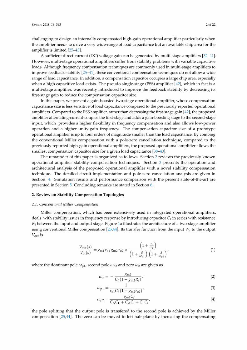
Miller compensation, which has been extensively used in integrated operational amplifiers,deals with stability issues in frequency response by introducing capacitor Cf in series with resistanceRf between the input and output stage. Figure 1a illustrates the architecture of a two-stage amplifierusing conventional Miller compensation [25,44]. Its transfer function from the input Vin to the outputVout is
Vout(s)Vin(s)
= gm1 ro1 gm2 ro2 ×
(1 + S
ωz
)(
1 + Sωp1
) (1 + S
ωp2
) , (1)
where the dominant pole ωp1, second pole ωp2 and zero ωz are given as
ωz = − gm2
Cf (1− gm2Rf), (2)
ωp1 =1
ro1Cf (1 + gm2ro2), (3)
ωp2 =gm2Cf
CACL + CACf + CLCf, (4)
the pole splitting that the output pole is transfered to the second pole is achieved by the Millercompensation [25,44]. The zero can be moved to left half plane by increasing the compensating
Sensors 2018, 18, 393 3 of 22
resistance value Rf. Assuming that intrinsic capacitance CA is much smaller than load capacitance CL
and compensation capacitance Cf, the unity gain frequency ωu is gm1/Cf, results in
ωp2
ωu=
gm2 Cfgm1 CL
. (5)
To avoid the unity gain frequency higher than ωp2, which may cause stability issues,the compensating capacitance must be designed larger than CLgm1/gm2. Therefore, the conventionalMiller compensation topology meets tremendous challenges in driving large capacitive load with alimited footprint.
ro1
Cf Rf
ro2CACL
ro1
Cf
ro2CA CL
VDDI1
I1
Io
Vout Vout
VinVin
gm1 gm2
ro1 ro2CA
CL
VoutVin
(a) (b)
(d)
Virtual
Ground
Rm
gm1gm1 gm2gm2
Cf Cf
CL
M1
VDD
M3
M2M4
CI1CI1 I1
Vin Vout
(c)
Figure 1. (a) Conventional Miller frequency compensation [25]. (b) Ahuja frequency compensation [26].(c) Conventional feedforward frequency compensation [27]. (d) Pseudo single-stage amplifier [42].(Diagrams were redrawn with simplification in order to facilitate the comparison among differentcompensation techniques.)
2.2. Ahuja Compensation
An improved compensation technique was introduced by Ahuja. It utilizes the current transformerproviding virtual ground to eliminate feed-forward path in Miller compensation [26], as shown inFigure 1b. The dominant pole ωp1 is lightly changed from (3) to
ωp1 =1
ro1Cf gm2ro2, (6)
while the second pole ωp2 now is
ωp2 =gm2 Cf
CA(CL + Cf), (7)
which is higher than (4) [27]. The unity gain frequency ωu is still given by gm1/Cf. As a result, the ratiobetween the second pole ωp2 and unity gain frequency ωu is augmented to
ωp2
ωu=
gm2
gm1
CfCA
CfCf + CL
. (8)

Sensors 2018, 18, 393 4 of 22
Compared to the conventional Miller compensation, a smaller compensating capacitance isrequired to drive a same load capacitance for a given phase margin. It copes better with heavycapacitive load [26,45]. However, this reduction is still heavily restricted by the capacitive load.
2.3. Conventional Feedforward Compensation
The feedforward compensation technique is introduced to obtain high-frequency performance byimplementing pole-zero cancellation [46,47]. Its principle in a folded-cascode amplifier is illustrated inFigure 1c. Assuming poles are widely spread, the positions of zeros and poles are approximately given by
ωz =gm2
(Cf + CBD2), (9)
ωp1 =1
ro C1, (10)
ωp2 =gm2[
C2 + C3 + Cf +(Cf+CBD2)(C2+CBD1)
C1
] , (11)
where C1 = CL + CGD2, C2 = CI1 + CGS1, C2 = CBD1 + CBD2, and the ro is the output impedance ofthis amplifier [27]. For the amplifier without Cf, the zero is much higher than the second pole asCBD2 is normally much smaller than the capacitors of the second pole. By inserting the feedforwardcapacitance Cf, the zero ωz shifts to lower frequency and is practical to cancel the second pole ωp2.However, due to the parasitic capacitances, mismatch between the zero and the second pole alwaysexists. It should be noted that the second pole also shifts to lower position, because of Cf, eventhough with a minor degree. Consequently, a relatively large Cf is needed to alleviate this mismatch.This limitation can be relieved by adding a resistance Rf in series with Cf [27].
2.4. Pseudo Single-Stage Amplifier
The single-stage amplifier only have one high-impedance node at its output, that is why it candrive a large load capacitance without any stability issues. For the pseudo single-stage amplifier, anintroduced intermediate resistance Rm is paralleled with first-stage output impedance ro1, as shownin Figure 1d, it significantly reduces the output impedance of first stage. Its dominant pole ωp1 andsecond pole ωp2 are obtained as
ωp1 =1
ro2 CL, (12)
ωp2 =1
(ro1||Rm)CA, (13)
because of the small Rm, the second pole is much higher than the dominant pole [42]. This two-stageamplifier has a frequency response similar to a single-stage amplifier without compensationcapacitance. However, this topology is implemented at the expense of insufficient DC voltage gain.This problem can be alleviated by adding a gain booster to the schematic.
In summary, there are mainly two problems existing in these previous frequency compensationtopologies. First, the size of compensation capacitor is tightly limited by the load capacitance.Specifically, for a 1-nF load capacitance, the compensation capacitance needed to address stability issuesis conventionally larger than 10 pF, which occupies a large proportion of the chip area. In addition,these techniques are required to be optimized based on the single specific load capacitance. As aresult, the wide range of load capacitance cannot be driven. In next section, a novel two-stageoperational amplifier is introduced to solve these two problems by combing Miller compensation andpole-zero cancellation.
Sensors 2018, 18, 393 5 of 22
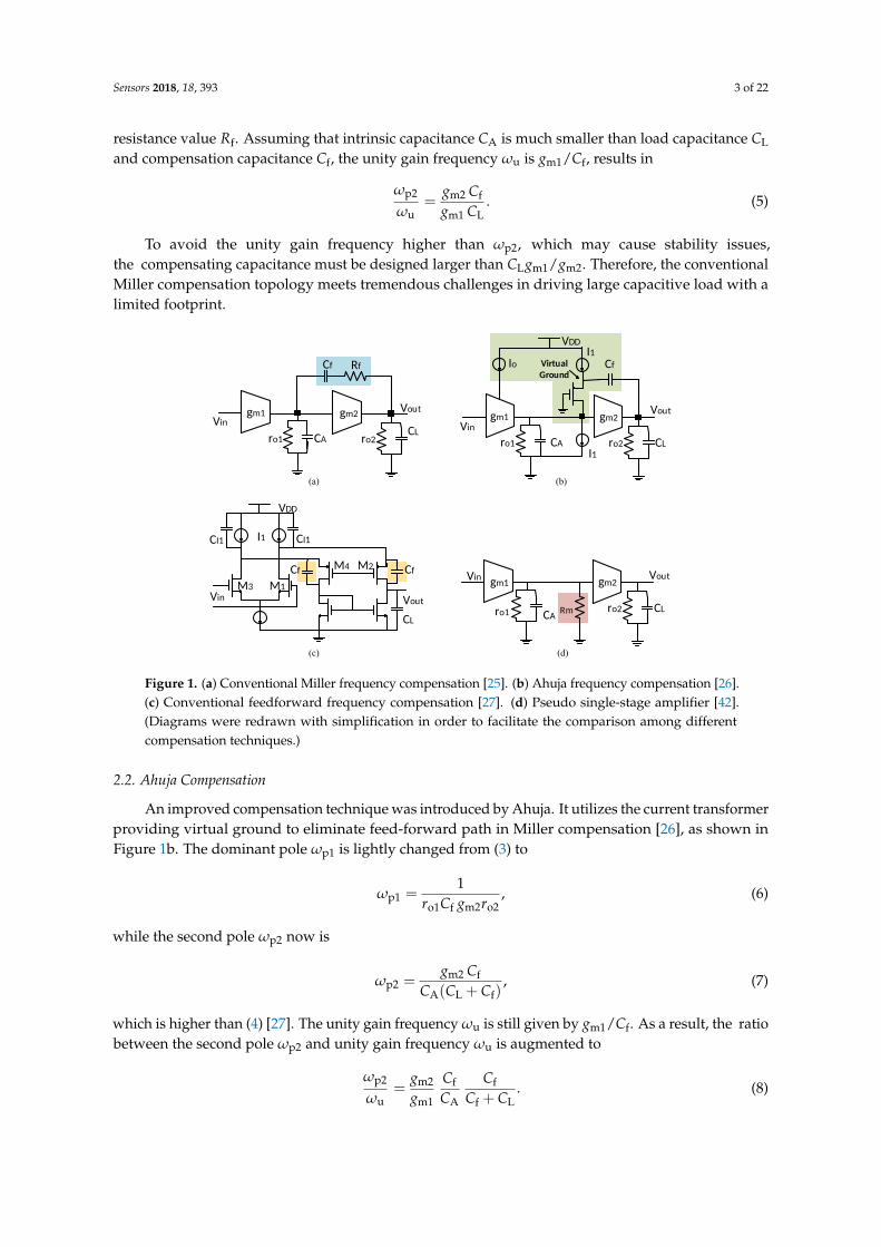
3. Proposed Architecture
The proposed operational amplifier architecture is illustrated in Figure 2. It consists of a mainamplifier, a gain booster, and a Class-B output stage.
gm1 gm2
gma gmb
ro1 ro2C1
Vin
roa1
RfCf
Vout
Rm
Class
B
CL
Cm
Gain Booster
Main Amplifier
A
C2
roa2
roB
CB
B
Figure 2. Architecture of the proposed gain-boosted two-stage operational amplifier withload-insensitive stability compensation.
In the main amplifier, the first stage transconductance gm1 is alternating-current (AC) coupledto the second stage transconductance gm2 through the capacitor Cm, the voltage gain at point A isgenerated by the gain booster. The transfer function from the input Vin to the point A VA is
VA(s)Vin(s)
= gma
roa1||
(Rf +
1s Cf
)1 + gmb(roa2||ro1||Rm)
× gmb
[Rm||roa2||ro1||
1s (C2 + C1||Cm)
], (14)
where gma and gmb are the transconductance, roa1 and roa2 are the output impedance, of the first andsecond stage of gain booster, respectively. ro1 is the output impedance of the first stage, and Rm is theinter-stage load impedance, in main amplifier. Because of the Miller effect, the impedance of Cf inseries with Rf is amplified by [1 + gmb(roa2||Rm)], where gmb(roa2||Rm) is the DC voltage gain of thesecond stage of gain booster. The voltage gain between A and B is
VB(s)VA(s)
= gm2
(ro2||
1s CB
), (15)
where ro2 is the output impedance of the second stage of main amplifier. Therefore, the overall transferfunction from the input Vin to the output Vout is obtained as
Vout(s)Vin(s)
=VA(s)Vin(s)
× VB(s)VA(s)
× Vout(s)VB(s)
= gma
roa1||
(Rf +
1s Cf
)1 + gmb(roa2||ro1||Rm)
× gmb
[Rm||roa2||ro1||
1s (C2 + C1||Cm)
]
× gm2
(ro2||
1s CB
)gmB
(roB||
1s CL
),
(16)
where gmB and roB is the transconductance and output impedance of the Class-B output stage,respectively. Compared to other capacitors in this function, CB is much smaller and negligible.This function is approximated to
Vout(s)Vin(s)
' gma roa1 gmb (roa2||Rm) gm2 ro2 gmB roB ×
(1 + S
ωzg
)(
1 + Sωpg
) (1 + S
ωp1
) (1 + S
ωp2
) , (17)

Sensors 2018, 18, 393 6 of 22
where
ωzg =1
Cf Rf, (18)
ωpg =1
roa1 Cf gmb(roa2||Rm), (19)
ωp1 =1
roBCL, (20)
ωp2 =1
(Rm||ro1||roa2) (C1||Cm + C2). (21)
Note that ωpg is the dominant pole introduced by the gain booster, and ωzg is the zero of thegain booster. ωp1 is the amplifier output node pole, and ωp2 is the pole from node A, and gmB is thetransconductance of the Class-B output stage.
Figure 3 illustrates the frequency response of the proposed amplifier. The DC gain is boosted bygmaroa1. The gain booster not only increases the DC gain of the main amplifier, but also moves thedominant pole from ωp1 to ωpg, which is independent of CL, as shown in Equation (19). However,the extra pole from the gain booster output node reduces the overall phase margin. The Millercompensation by Cf and Rf in the gain booster alleviates this problem. The zero of the gain boosterωzg is designed to cancel the output node pole, ωp1, by choosing a suitable Cf and Rf. The pole-zerocancellation enable the proposed work to drive a wide range of load capacitance. The compensationcapacitor size comparison between the pseudo single-stage (PSS) amplifier amplifier and this workis given in Table 1. Compared to a PSS amplifier, by taking advantage of Miller compensation, theproposed amplifier reduces the compensation capacitor size by ten times while providing the sameDC gain and unity gain bandwidth (UGBW).
0
Gain Booster
ω (radian)
|Vo(s)/Vi(s)|(dB)
ωp1(=ωzg)
p2
pg
Avo
p1(=zg)
p2 pg
Ims
Res
Pole-Zero Cancellation
pg: pole of the gain boosterzg: zero of the gain boosterp1: pole of output nodep2: pole of node A
Figure 3. The gain booster provides a dominant pole ωpg and the zero of the gain booster ωzg cancelsthe main amplifier output node pole ωp1, thereby making the second pole ωp2 independent of the loadcapacitance CL.
Table 1. Compensation capacitor size comparison between the PSS amplifier and this work.
PSS Amplifier [42] This Work
Second Pole 1/[(C1 + C2)(ro1||roa2||Rm)] 1/[(C1||Cm + C2)(ro1||roa2||Rm)]UGBW Av/(Cfroa1) Av/[Cfroa1gmb(roa2||Rm)]
Cf 1 ≈1/[gmb(roa2||Rm)] ≈ 0.1
Note: The same second pole location and unity-gain bandwidth (UGBW) are assumed.

Sensors 2018, 18, 393 7 of 22
The stability of the operational amplifier is dominated by its phase margin, which is the differencebetween the phase and 180 at the unity-gain cut-off frequency. For a two-pole system, assuming polesare widely spread, its phase margin (PM) is given as
PM = 180 − 180
πtan−1
(ωu
ωp1
)− 180
πtan−1
(ωu
ωp2
)' 90 − 180
πtan−1
(ωu
ωp2
),
(22)
where the ωp1 and the ωp2 are the dominant and second pole respectively, the ωu is the unity gainfrequency. For the proposed work, the phase margin is primarily determined by the pole from thenode A, ωp2, as shown in (21), which is not affected by the load capacitance CL. The capacitance atnode A is much smaller than the compensation capacitance and load capacitance. The gain booster andRm raise the second pole location from 1/(CAro1) to 1/[CA(ro1||roa2||Rm)] where CA is approximatelybut less than (C1 + C2) and Cm is designed to be much larger than C1 and C2. Then the ratiobetween the second pole and the unity gain frequency is increased, which broadens the phase margin.Compared to the design without gm1, the proposed amplifier moves ωp2 higher from 1/(CA(roa2||Rm))
to 1/[CA(ro1||roa2||Rm)]. The comparison about frequency response bode plots among this work,the PSS amplifier [42] and the design without gm1 is shown in Figure 4. With same compensation andload capacitance, this work achieves a larger phase margin and wider unity gain bandwidth.
0p2
Avo
: This work: PSS amplifier: GB + gm2
pg
PM for This work PM for
GB+gm2
PM for PSS amplifier
0
90
180
p2 for this work:
1/[(Rm||ro1||roa2)(C1||Cm+C2)]
p2 for PSS amplifier:
1/[(Rm||ro1||roa2)(C1+C2)]
p2 for GB+gm2:
1/[(Rm||roa2)(C1||Cm+C2)]
Note: Same compensation and load capacitances are assumed
Ga
in R
esp
on
seP
ha
se R
esp
on
se
pg for this work:
1/[roa1Cfgmb(Rm||roa2)]
pg for PSS amplifier:
1/(roa1Cf)
p1=zg
(radian)
(radian)
zg of PSS amplifier
Figure 4. Frequency response for this work, the PSS amplifier [42] and the design without the firststage of main amplifier (GB+ gm2).
While the two-stage amplifier implementing conventional Miller compensation has a second poledetermined by the load capacitance, as shown in Equation (4), the dominant and second pole of thiswork. which are shown in EquationS (19) and (21), are both independent of the load capacitance.As a result, this work can maintain a sufficient phase margin with various load capacitance, and thisfrequency compensation topology is less sensitive to the load capacitance compared to the conventionalMiller compensation.

Sensors 2018, 18, 393 8 of 22
4. Circuit Implementation and Analysis
4.1. Circuit Implementation
Figure 5 shows the circuit of the proposed operational amplifier. Its transistor size is shown inTable 2. The composite cascode [48] is used as input stage in both the main amplifier and the gainbooster in order to obtain sufficient DC voltage gain. Compared to the single transistor with doubledlength, the composite pair can provide higher gain. A previous work indicated that the voltage gainexceeding 80 dB per stage can be achieved by the composite cascode configuration with transistorsoperating in weak or moderate inversion domain [49]. A Class-B output stage is implemented toprovide a fast settling time by improving the amplifier slew rate.
M1 M2
M3 M4
M5 M6
M7 M8M10 M11
M17M16
M12 M13
M9M14 M15
M21M20
M18 M19
1A 1A
0.15A
0.5A 0.5A
0.5A Vin+Vin-
Rv=1K
M22 M23
M38
M39
Main Amplifier
0.5A
1A
M24 M25
M26 M27
M28
M30
M29
M31
M32
M33
M34
Miller Compensation
M35
M36 M37
5nA 5nA
1A
Gain Booster
Vout
Rf
50M
Cf
200fF
Vin+Vin-
Vb1
Vb2Vb2
Vb3Vb3
Vb4Vb4Vb5
Vb7
Vb6
Vb8
VDD
Figure 5. Schematic of the proposed gain-boosted two-stage operational amplifier with load-insensitivestability compensation.
Table 2. Transistors size of the proposed work.
Device Size (µm/µm) Device Size (µm/µm) Device Size (µm/µm)
M1, M2 1.7/2.5 M3, M4 6.55/0.17 M5, M6 4/0.13M7, M8 0.13/0.14 M9 3.3/0.2 M10, M11 5/1
M12, M13 20/1 M14, M15 7.5/1 M16, M17 0.2/0.24M18, M19 0.15/0.16 M20 0.15/2.52 M21 0.15/1.35M22, M23 5/5 M24, M25 0.13/26 M26, M27 0.13/0.38M28, M29 0.15/0.3 M30, M31 0.15/12.05 M32 0.15/0.16
M33 0.32/0.17 M34 0.2/0.2 M35 10/5M36, M37 0.29/0.13 M38 0.7/0.13 M39 0.8/0.13
Design parameters of the proposed amplifier are shown in Table 3. The inter-stage load resistanceRm can be realized by a negative feedback loop as
Rm =1
gmv+
2gmf Rv gmv
, (23)
where the gmv is the transconductance of M16 and M17, and the gmf is the transconductance of M12
and M13 [42]. The Rm is optimized though choosing suitable gmv and gmf to make the second pole ωp2
much higher than unity gain frequency to obtain sufficient phase margin. Rf is replaced by floatingtunable CMOS resistors to reduce the chip area [50]. The bias circuit for this work is illustrated inFigure A1 and Table A1.
Sensors 2018, 18, 393 9 of 22
Table 3. Design parameters of the proposed work.
Transconductance Value (µS) Transconductance Value (µS)gm1 13.1 gm2 15.0gma 0.094 gmb 13.2
Capacitance Value (fF) Capacitance Value (fF)Cm 100 Cf 200
Resistance Value (MΩ) Resistance Value (MΩ)Rm 20 Rf 50
4.2. Pole-Zero Cancellation and Sensitivity Analysis
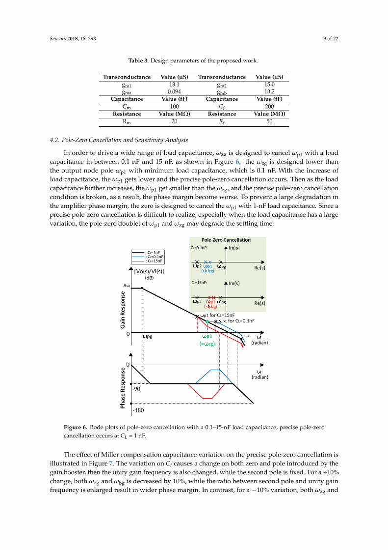
In order to drive a wide range of load capacitance, ωzg is designed to cancel ωp1 with a loadcapacitance in-between 0.1 nF and 15 nF, as shown in Figure 6. the ωzg is designed lower thanthe output node pole ωp1 with minimum load capacitance, which is 0.1 nF. With the increase ofload capacitance, the ωp1 gets lower and the precise pole-zero cancellation occurs. Then as the loadcapacitance further increases, the ωp1 get smaller than the ωzg, and the precise pole-zero cancellationcondition is broken, as a result, the phase margin become worse. To prevent a large degradation inthe amplifier phase margin, the zero is designed to cancel the ωp1 with 1-nF load capacitance. Since aprecise pole-zero cancellation is difficult to realize, especially when the load capacitance has a largevariation, the pole-zero doublet of ωp1 and ωzg may degrade the settling time.
0
(radian)
|Vo(s)/Vi(s)|(dB)
p1
(=zg)
p2pg
Avo
p1 for CL=0.1nFp1 for CL=15nF
: CL=1nF: CL=0.1nF: CL=15nF
p1(>zg)
p2 pg Res
p1(<zg)
p2 pg Res
Pole-Zero Cancellation
CL=15nF: Ims
ImsCL=0.1nF:
0
-90
-180
(radian)
Ga
in R
esp
on
seP
ha
se R
esp
on
se
Figure 6. Bode plots of pole-zero cancellation with a 0.1–15-nF load capacitance, precise pole-zerocancellation occurs at CL = 1 nF.
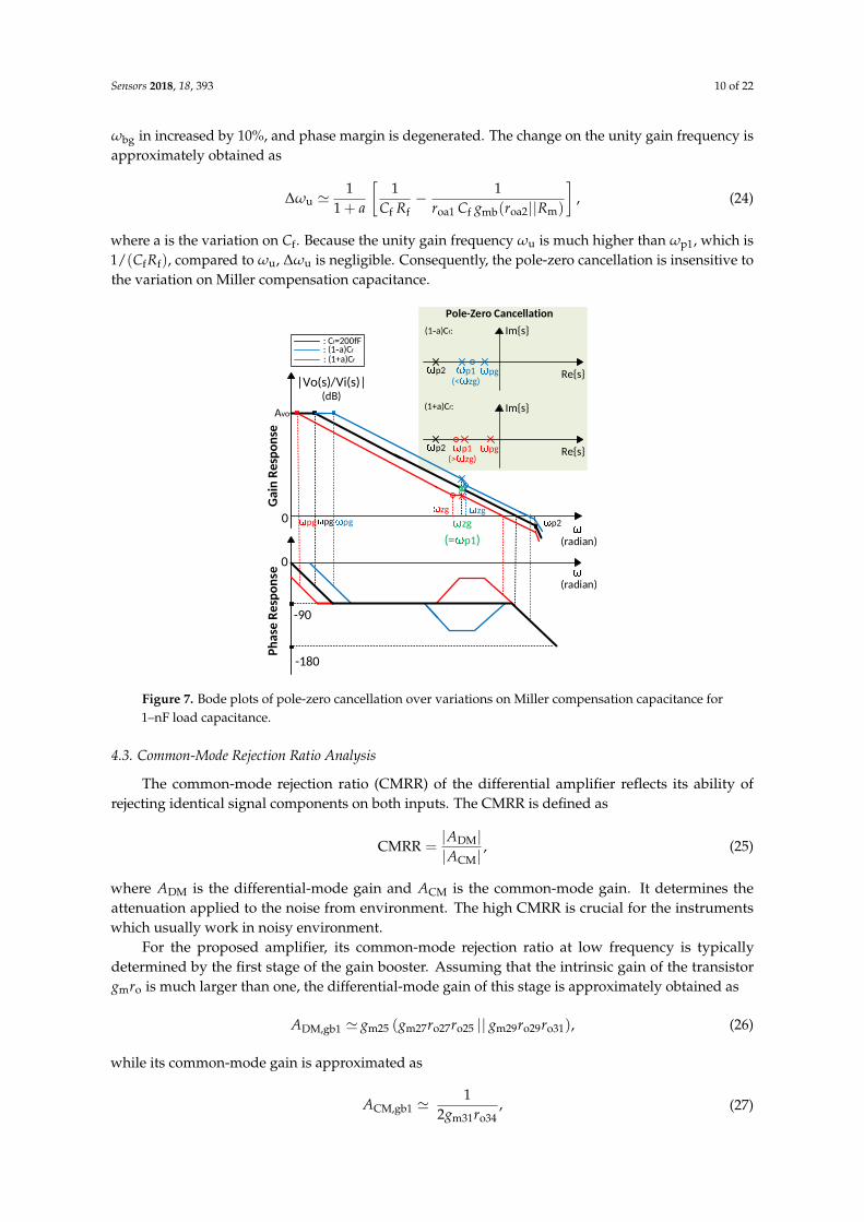
The effect of Miller compensation capacitance variation on the precise pole-zero cancellation isillustrated in Figure 7. The variation on Cf causes a change on both zero and pole introduced by thegain booster, then the unity gain frequency is also changed, while the second pole is fixed. For a +10%change, both ωzg and ωbg is decreased by 10%, while the ratio between second pole and unity gainfrequency is enlarged result in wider phase margin. In contrast, for a −10% variation, both ωzg and
Sensors 2018, 18, 393 10 of 22
ωbg in increased by 10%, and phase margin is degenerated. The change on the unity gain frequency isapproximately obtained as
∆ωu '1
1 + a
[1
Cf Rf− 1
roa1 Cf gmb(roa2||Rm)
], (24)
where a is the variation on Cf. Because the unity gain frequency ωu is much higher than ωp1, which is1/(CfRf), compared to ωu, ∆ωu is negligible. Consequently, the pole-zero cancellation is insensitive tothe variation on Miller compensation capacitance.
0
|Vo(s)/Vi(s)|(dB)
zg
(=p1)
p2pg
Avo
zgzg
: Cf=200fF: (1-a)Cf
: (1+a)Cf
p1(<zg)
p2 pg Res
p1(>zg)
p2 pg Res
Pole-Zero Cancellation
(1+a)Cf: Ims
Ims(1-a)Cf:
pg pg
0
-90
-180
Ph
ase
Re
spo
nse
Ga
in R
esp
on
se
(radian)
(radian)
Figure 7. Bode plots of pole-zero cancellation over variations on Miller compensation capacitance for1–nF load capacitance.
4.3. Common-Mode Rejection Ratio Analysis
The common-mode rejection ratio (CMRR) of the differential amplifier reflects its ability ofrejecting identical signal components on both inputs. The CMRR is defined as
CMRR =|ADM||ACM|
, (25)
where ADM is the differential-mode gain and ACM is the common-mode gain. It determines theattenuation applied to the noise from environment. The high CMRR is crucial for the instrumentswhich usually work in noisy environment.
For the proposed amplifier, its common-mode rejection ratio at low frequency is typicallydetermined by the first stage of the gain booster. Assuming that the intrinsic gain of the transistorgmro is much larger than one, the differential-mode gain of this stage is approximately obtained as
ADM,gb1 ' gm25 (gm27ro27ro25 || gm29ro29ro31), (26)
while its common-mode gain is approximated as
ACM,gb1 '1
2gm31ro34, (27)

Sensors 2018, 18, 393 11 of 22
Then the CMRR of the proposed work at DC is
CMRR =|ADM,gb1||ACM,gb1|
=1
2gm31ro34× gm25(gm27ro27ro25 || gm29ro29ro31)
= 104 dB,
(28)
which is close to the simulated CMRR of 109 dB.
5. Simulation Results and Discussion
The proposed amplifier is designed using a 130-nm CMOS technology with a total area of0.00090 mm2. Its layout is shown in Figure 8. The proposed amplifier without bias circuit occupies0.00073-mm2 chip area. The total stability compensation area is 100 µm2.
The stability simulation with 0.05–17 nF load capacitance over Miller compensation capacitancesvariations are shown in Figures 9 and 10 and Tables 4 and 5. For the prototype amplifier, the maximumphase margin is achieved when load capacitance CL is 2.5 nF, which is 91. The phase margin largerthan 70 with a load capacitance of 0.2–12 nF and it becomes less than 65 when the load capacitanceexceeds the 0.1–15-nF range. With the 30% variation on Miller compensation capacitance, the largestchange in phase margin is less than 8% and demonstrates a good tolerance on process variation.
Cm Cm
A
B
Cf
C
32m
28
m
A. Main Amplifier
B. Gain Booster
C. Bias Circuit
Figure 8. Layout of the proposed amplifier in 130-nm technology.
Figure 9. Simulated phase margin of the proposed amplifier with 0.05–17 nF load capacitance overMiller compensation capacitance variations.

Sensors 2018, 18, 393 12 of 22
Table 4. Phase margin over variations on Miller compensation capacitor.
CL (nF) This Work 70% Cf 80% Cf 90% Cf 110% Cf 120% Cf 130% Cf
0.08 59.5 55.5 57.2 58.8 60.7 62.7 63.0
0.1 65.2 62.1 63.5 64.7 66.2 67.7 67.9
0.2 73.7 71.0 72.2 73.1 74.8 76.0 77.4
0.5 77.7 76.2 76.8 77.4 78.1 78.9 79.1
1 82.9 80.8 81.7 82.5 83.6 84.6 84.9
2.5 90.9 88.4 89.5 90.3 91.7 92.2 92.9
7 80.9 76.3 78.1 79.5 82.0 82.8 83.7
12 70.2 65.2 66.6 68.5 71.5 72.3 73.1
15 65.8 59.1 61.4 63.3 66.9 68.0 69.5
16 63.9 58.8 60.0 61.9 65.5 66.5 68.1
Figure 10. Simulated gain margin of the proposed amplifier with 0.05–17 nF load capacitance overMiller compensation capacitance variations.
Table 5. Gain margin over variations on Miller compensation capacitor.
CL (nF) This Work 70% Cf 80% Cf 90% Cf 110% Cf 120% Cf 130% Cf
0.08 8.9 dB 5.0 dB 7.1 dB 8.5 dB 10.6 dB 11.4 dB 12.5 dB0.1 10.9 dB 6.2 dB 8.4 dB 10.1 dB 11.2 dB 12.0 dB 13.8 dB0.2 11.2 dB 7.1 dB 9.0 dB 10.8 dB 11.9 dB 13.0 dB 14.8 dB0.5 13.6 dB 9.7 dB 11.0 dB 12.8 dB 14.2 dB 15.4 dB 16.1 dB1 28.3 dB 25.4 dB 26.6 dB 27.9 dB 29.4 dB 30.5 dB 31.2 dB
2.5 36.2 dB 32.0 dB 33.4 dB 35.6 dB 37.0 dB 37.8 dB 38.9 dB7 45.2 dB 41.9 dB 43.1 dB 44.5 dB 46.4 dB 47.7 dB 48.2 dB
12 49.6 dB 46.8 dB 47.6 dB 48.9 dB 51.2 dB 52.1 dB 53.0 dB15 51.3 dB 48.4 dB 49.3 dB 50.7 dB 52.4 dB 53.0 dB 54.1 dB16 52.0 dB 48.2 dB 49.6 dB 51.3 dB 53.2 dB 54.1 dB 55.9 dB
The simulated frequency response with a 2.5-nF load capacitance is shown in Figure 11,demonstrating 130-kHz unity-gain frequency and over 100-dB gain at DC. The frequency response ofthe amplifier without the gain booster is separately simulated, which is labeled as gm1 + gm2, showinga significant DC gain drop as expected from the AC coupling between gm1 and gm2. In addition,the frequency response of the amplifier without the first stage of the main amplifier (gm1) is alsosimulated, which is labeled as GB + gm2, showing 16 degradation in the phase margin. It also showsthat the first stage transconductance allows the overall amplifier to provide a sufficient gain at the

Sensors 2018, 18, 393 13 of 22
frequencies higher than 50 kHz. Figure 12 shows the comparison of simulated frequency responseamong this work, the pseudo single-stage (PSS) amplifier and the design without Cm using totalcompensation capacitance of 400-fF. Because the 400-fF compensation capacitance is far from sufficientfor the PSS amplifier to implement pole-zero cancellation, its phase margin is degenerated severely.
Figure 11. Simulated frequency response of the proposed amplifier with 2.5-nF load capacitance.
Figure 12. Comparison of simulated frequency response among this work, the PSS amplifier [42] andthe design without Cm with 2.5-nF load capacitance and 400-fF total compensation capacitance.
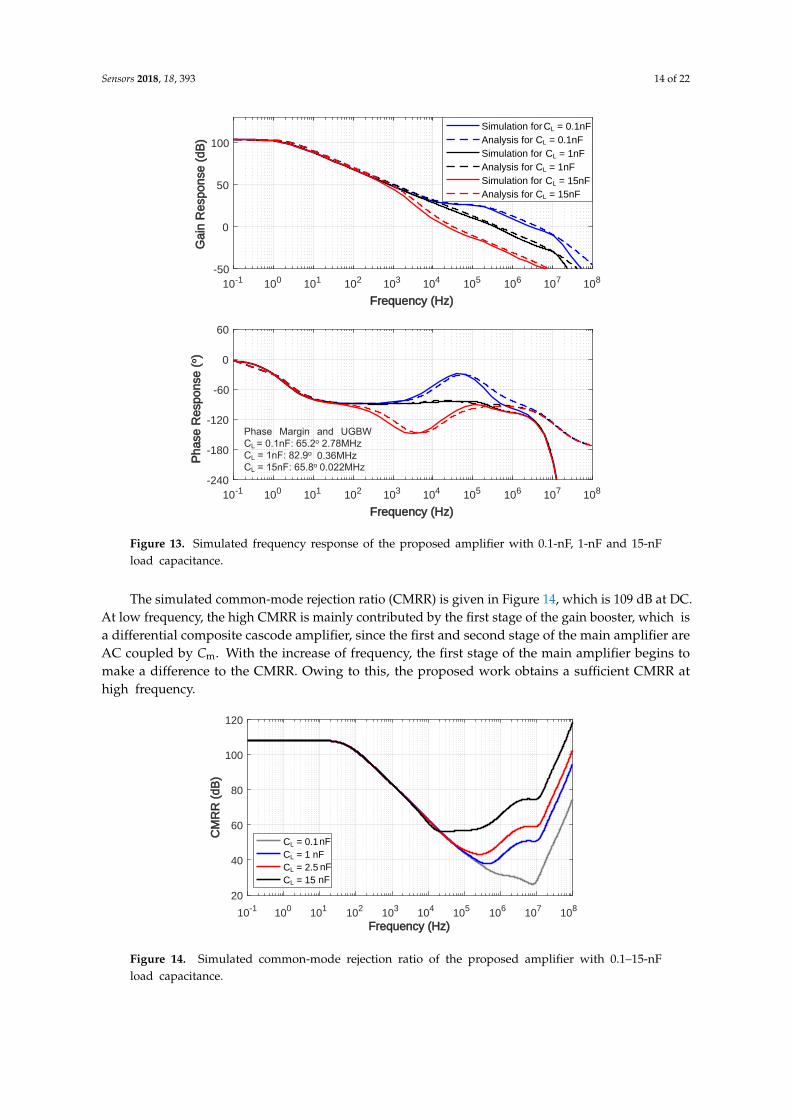
Figure 13 illustrates the simulated frequency response of the proposed amplifier with 0.1-nF,1-nF and 15-nF load capacitances, respectively. The precise pole-zero cancellation occurs when loadcapacitance is 1 nF. The frequency response for 0.1-nF load capacitance shows that the pole of thegain booster, ωgz is lower than the output node pole ωp1, while ωgz is higher than ωp1 when loadcapacitance is 15 nF. The broken pole-zero cancellation reflected in Figure 13 accords with the analysisin previous section.
Sensors 2018, 18, 393 14 of 22
10-1 100 101 102 105 106 107 108103 104
Frequency (Hz)
-50
0
50
100
Gai
n R
espo
nse
(dB
)
10-1 100 101 102 105 106 107 108103 104
Frequency (Hz)
-240
-180
-120
-60
0
60
Pha
se R
espo
nse
(o)
Simulation for CL = 0.1nFAnalysis for CL = 0.1nFSimulation for CL = 1nFAnalysis for CL = 1nFSimulation for CL = 15nFAnalysis for CL = 15nF
Phase Margin and UGBW CL
= 0.1nF: 65.2o 2.78MHz0.36MHzCL = 1nF: 82.9o
CL = 15nF: 65.8o 0.022MHz
Figure 13. Simulated frequency response of the proposed amplifier with 0.1-nF, 1-nF and 15-nFload capacitance.
The simulated common-mode rejection ratio (CMRR) is given in Figure 14, which is 109 dB at DC.At low frequency, the high CMRR is mainly contributed by the first stage of the gain booster, which isa differential composite cascode amplifier, since the first and second stage of the main amplifier areAC coupled by Cm. With the increase of frequency, the first stage of the main amplifier begins tomake a difference to the CMRR. Owing to this, the proposed work obtains a sufficient CMRR athigh frequency.
10-1 100 101 102 103 104 105 106 107 108
Frequency (Hz)
20
40
60
80
100
120
CM
RR
(dB
)
CL = 0.1 nFCL = 1 nFCL = 2.5 nFCL = 15 nF
Figure 14. Simulated common-mode rejection ratio of the proposed amplifier with 0.1–15-nFload capacitance.

Sensors 2018, 18, 393 15 of 22
Under a transient simulation setup illustrated in Figure 15, a step response simulation withvarious load capacitance is shown in Figure 16, and the simulated 1% settling time with variationon Miller compensation capacitor Cf is shown in Figure 17. The 1% settling time is damaged dueto exceeding-80 phase margin when driving 1–7-nF load capacitance. With the diminution of Cf,the phase margin decreases, then the 1% settling time is improved.
Vout
CL
+
_
0.50V
0.63V
Figure 15. Test-bench circuit for step response simulation.
0 1 2 3 4 5
Time (μs)
0.46
0.5
0.54
0.58
0.62
0.66
Vol
tage
(V
)
CL = 0.1 nFCL = 0.2 nFCL = 0.5 nFCL = 1 nF
0 20 40 60 80 100 120
Time (μs)
0.46
0.5
0.54
0.58
0.62
0.66
0.7
Vol
tage
(V
)
CL = 2.5 nFCL = 5 nFCL = 10 nFCL = 15 nF
Figure 16. Simulated step response of the proposed amplifier with various load capacitance.
Figure 17. Simulated 1% settling time of the proposed amplifier with 0.1–15-nF load capacitance overMiller compensation capacitor variations.

Sensors 2018, 18, 393 16 of 22
The input common-mode range (ICMR) and output swing of the proposed amplifier are shownin Figure 18. The input common range is from 0.49 V to 0.64 V, and the output bias voltage swingsbetween 0.34 V and 0.68 V. Considering that the Class-B output stage may cause the distortion ofoutput signal, the simulated total harmonic distortion (THD) with 40-mVpp differential input whenload capacitance is 0.1 nF, 1 nF and 15 nF is shown in Figure 19. The largest total harmonic distortionis −114 dB, while the DC voltage gain is 103 dB.
Figure 18. Simulated (a) input common-mode range (b) output swing of the proposed amplifier.
10-2 10-1 100 101 102 103 104 105
Frequency (Hz)
-110
-120
-130
-140
-150
Tota
l Har
mon
ic D
isto
rtio
n (d
B)
CL = 1 nFCL = 0.1 nFCL = 15 nF
Figure 19. Simulated total harmonic distortion of the proposed amplifier with 0.1-nF, 1-nF and 15-nFload capacitance.
Monte Carlo simulations with 50 samples for DC gain, unity gain bandwidth and phase marginwith 1-nF load capacitance are shown in Figure 20. The median performance of 97.5-dB gain, 293.5-kHzunity gain frequency, and 87.4 phase margin is obtained with a standard deviation of 10.7 dB, 82.2 kHz,and 16.8. Considering the limited number of samples, the median performance of the Monte Carlosimulation well matches the simulation results with typical case model. Figure 20c shows that theprototype remains stable with 2σ variation. In addition, the corner simulation performed with one σ
process variation presents 110.3-dB gain, 329.9-kHz unity gain bandwidth and 82 phase margin athigh side and 95.5-dB gain, 227.3-kHz unity gain band width and 93 phase margin at low side, whichalso matches the statistical distributions from the Monte Carlo simulation.
Table 6 compares the simulated performance of the prototype design with the state-of-the-art.Compared to previous works, this work utilizes the smallest compensation capacitance, which is 400 fF,and demonstrates the highest ratio between load capacitance and total compensation capacitance,
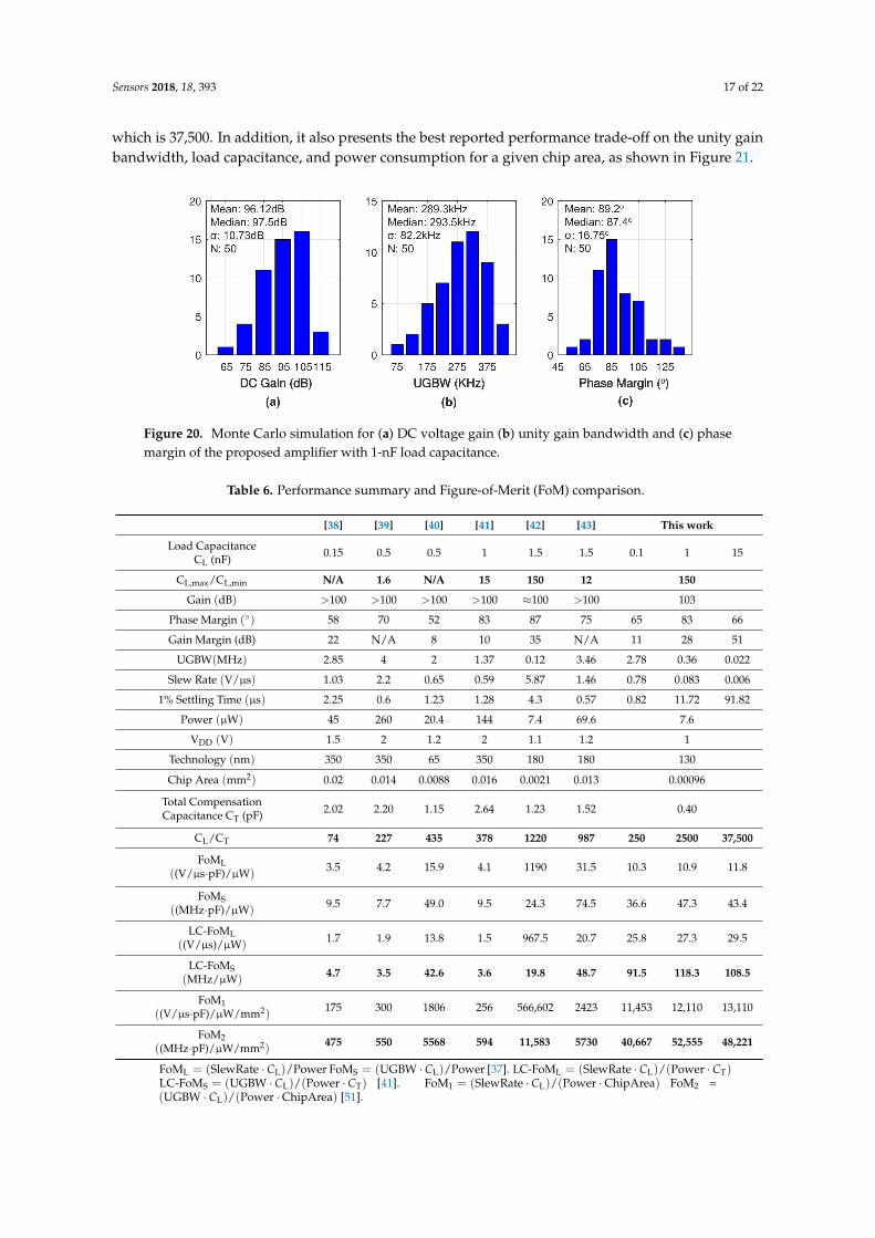
Sensors 2018, 18, 393 17 of 22
which is 37,500. In addition, it also presents the best reported performance trade-off on the unity gainbandwidth, load capacitance, and power consumption for a given chip area, as shown in Figure 21.
Figure 20. Monte Carlo simulation for (a) DC voltage gain (b) unity gain bandwidth and (c) phasemargin of the proposed amplifier with 1-nF load capacitance.
Table 6. Performance summary and Figure-of-Merit (FoM) comparison.
[38] [39] [40] [41] [42] [43] This work
Load CapacitanceCL (nF)
0.15 0.5 0.5 1 1.5 1.5 0.1 1 15
CL,max/CL,min N/A 1.6 N/A 15 150 12 150
Gain (dB) >100 >100 >100 >100 ≈100 >100 103
Phase Margin () 58 70 52 83 87 75 65 83 66
Gain Margin (dB) 22 N/A 8 10 35 N/A 11 28 51
UGBW(MHz) 2.85 4 2 1.37 0.12 3.46 2.78 0.36 0.022
Slew Rate (V/µs) 1.03 2.2 0.65 0.59 5.87 1.46 0.78 0.083 0.006
1% Settling Time (µs) 2.25 0.6 1.23 1.28 4.3 0.57 0.82 11.72 91.82
Power (µW) 45 260 20.4 144 7.4 69.6 7.6
VDD (V) 1.5 2 1.2 2 1.1 1.2 1
Technology (nm) 350 350 65 350 180 180 130
Chip Area (mm2) 0.02 0.014 0.0088 0.016 0.0021 0.013 0.00096
Total CompensationCapacitance CT (pF) 2.02 2.20 1.15 2.64 1.23 1.52 0.40
CL/CT 74 227 435 378 1220 987 250 2500 37,500
FoML((V/µs·pF)/µW)
3.5 4.2 15.9 4.1 1190 31.5 10.3 10.9 11.8
FoMS((MHz·pF)/µW)
9.5 7.7 49.0 9.5 24.3 74.5 36.6 47.3 43.4
LC-FoML((V/µs)/µW)
1.7 1.9 13.8 1.5 967.5 20.7 25.8 27.3 29.5
LC-FoMS(MHz/µW)
4.7 3.5 42.6 3.6 19.8 48.7 91.5 118.3 108.5
FoM1((V/µs·pF)/µW/mm2)
175 300 1806 256 566,602 2423 11,453 12,110 13,110
FoM2((MHz·pF)/µW/mm2)
475 550 5568 594 11,583 5730 40,667 52,555 48,221
FoML = (SlewRate · CL)/Power FoMS = (UGBW · CL)/Power [37]. LC-FoML = (SlewRate · CL)/(Power · CT)LC-FoMS = (UGBW · CL)/(Power · CT) [41]. FoM1 = (SlewRate · CL)/(Power ·ChipArea) FoM2 =(UGBW · CL)/(Power ·ChipArea) [51].

Sensors 2018, 18, 393 18 of 22
10-1 100 101
Load Capacitance CL (nF)
101
102
103
104
105C
L/C
T
10-1 100 101
Load Capacitance CL (nF)
0
20
40
60
80
100
120
140
LC-F
oMS (
MH
z/μW
)
10-1 100 101
Load Capacitance CL (nF)
102
103
104
105
FoM
2 ((
MH
z*pF
)/μW
/mm
2 )This workThis work
This work
[38]
[38]
[38]
[39]
[39]
[39][40][40]
[40][41]
[41][41]
[42]
[42]
[42]
[43][43]
[43]
Figure 21. Benchmark of CL/CT, LC-FoMs and FoM2 [38–43].
6. Conclusions
Transducers with nonlinear capacitive input impedance need an operational amplifier, which isstable for a wide range of load capacitance. Such an operational amplifier in a conventional designrequires a large area for compensation capacitors, increasing costs and limiting applications. In order toaddress this problem, we present a gain-boosted two-stage operational amplifier, whose frequencyresponse compensation is less sensitive to the load capacitance compared to the conventional Millerfrequency compensation. The proposed amplifier cancels the output node pole of the main amplifierstage by the zero of the gain booster, so that a sufficient phase margin can be achieved withoutusing a large compensation capacitor. A prototype CMOS amplifier designed with the proposedarchitecture uses two-to-four orders of magnitude smaller compensation capacitor compared to theload capacitance. This advantage in the compensation capacitor area requirement extends theapplications of the proposed operational amplifier beyond the transducer interface circuits and maybenefit general analog integrated circuit applications. The prototype CMOS operational amplifierdemonstrates the highest performance trade-off to date when considering unity-gain bandwidth, loadcapacitance, power consumption, and chip area, which can enable an a compact low-cost transducerinterface with unprecedentedly high resolution for emerging applications. It should be also notedthat the proposed operational amplifier design technique can be used not only with monolithicallyintegrated transducer interface circuits but also with transducer interface circuits assembled by discreteoff-the-shelf components.
Acknowledgments: This work was supported in part by Viterbi Postdoctoral Fellowship.
Author Contributions: Z.Y. refined the initial circuit topology, designed the prototype, performed the simulations,analyzed the data, and wrote the paper; S.C. conceived the topology and wrote the paper; X.Y. reviewed theprototype design and provided technical advice on the simulations and writing.
Conflicts of Interest: The authors declare no conflict of interest.
Sensors 2018, 18, 393 19 of 22
Abbreviations
The following abbreviations are used in this manuscript:
AC Alternating CurrentCMOS Complementary Metal-Oxide-SemiconductorCMRR Common-Mode Rejection RatioFoM Figure-of-MeritDC Direct CurrentICMR Input Common-Mode RangePM Phase MarginPSS Pseudo-Single StageUGBW Unity Gain Bandwidth
Appendix A
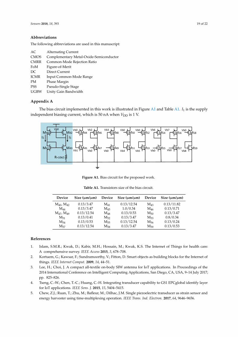
The bias circuit implemented in this work is illustrated in Figure A1 and Table A1. I1 is the supplyindependent biasing current, which is 50 nA when VDD is 1 V.
Vb0 Vb0
Vb0
Vb0 Vb0
Vb0 Vb0
Vb0
I1
Vb1
Vb2 Vb3
Vb4
I1
M40 M42
M41 M43
R=10k
M44
M45
M46
M47
M48
M49Vb0
M50
M51Vb5
M52
M53
Vb6M54
M55
M56
M57
Vb7M58
M59Vb8
Figure A1. Bias circuit for the proposed work.
Table A1. Transistors size of the bias circuit.
Device Size (µm/µm) Device Size (µm/µm) Device Size (µm/µm)
M40, M42 0.13/3.47 M41 0.13/12.54 M43 0.13/11.82M44 0.13/3.47 M45 1.0/0.34 M46 0.13/0.71
M47, M49 0.13/12.54 M48 0.13/0.53 M50 0.13/3.47M51 0.13/0.41 M52 0.13/3.47 M53 0.8/0.34M54 0.13/0.53 M55 0.13/12.54 M56 0.13/0.24M57 0.13/12.54 M58 0.13/3.47 M59 0.13/0.53
References
1. Islam, S.M.R.; Kwak, D.; Kabir, M.H.; Hossain, M.; Kwak, K.S. The Internet of Things for health care:A comprehensive survey. IEEE Access 2015, 3, 678–708.
2. Kortuem, G.; Kawsar, F.; Sundramoorthy, V.; Fitton, D. Smart objects as building blocks for the Internet ofthings. IEEE Internet Comput. 2009, 14, 44–51.
3. Lee, H.; Choi, J. A compact all-textile on-body SIW antenna for IoT applications. In Proceedings of the2014 International Conference on Intelligent Computing Applications, San Diego, CA, USA, 9–14 July 2017;pp. 825–826.
4. Tseng, C.-W.; Chen, T.-C.; Huang, C.-H. Integrating transducer capability to GS1 EPCglobal identify layerfor IoT applications. IEEE Sens. J. 2015, 15, 5404–5415.
5. Chew, Z.J.; Ruan, T.; Zhu, M.; Bafleur, M.; Dilhac, J.M. Single piezoelectric transducer as strain sensor andenergy harvester using time-multiplexing operation. IEEE Trans. Ind. Electron. 2017, 64, 9646–9656.

Sensors 2018, 18, 393 20 of 22
6. Vikulin, I.; Gorbachev, V.; Gorbacheva, A.; Krasova, V.; Polakov, S. Economical transducers of environmentalparameters to a frequency for the end devices of IoT. In Proceedings of the 2017 2nd International Conferenceon Advanced Information and Communication Technologies, Lviv, Ukraine, 4–7 July 2017; pp. 35–40.
7. Khyam, M.O.; Alam, M.J.; Lambert, A.J.; Garratt, M.A.; Pickering, M.R. High-precision OFDM-basedmultiple ultrasonic transducer positioning using a robust optimization approach. IEEE Sens. J. 2016, 16,5325–5336.
8. Wang, N.; Zhang, Z.; Li, Z.; He, Q.; Lin, F.; Lu, Y. Design and characterization of a low-cost self-oscillatingfluxgate transducer for precision measurement of high-current. IEEE Sens. J. 2016, 9, 2971–2981.
9. Yang, X.; Lee, H.-S. Design of a 4th-order multi-stage feedforward operational amplifier for continuous-timebandpass delta sigma modulators. In Proceedings of the 2016 IEEE International Symposium on Circuitsand Systems (ISCAS), Montreal, QC, Canada, 22–25 May 2016; pp. 1058–1061.
10. Chung, S.; Abediasl, H.; Hashemi, H. A monolithically integrated large-scale optical phased array insilicon-on-insulator CMOS. IEEE J. Solid-State Circuits 2018, 53, 275–296.
11. Ergun, A.S.; Hung, Y.; Zhuang, X.; Oralkan, O.; Yaralioglu, G.G.; Khuri-Yakub, B.T. Capacitivemicromachined ultrasonic transducers: Fabrication technology. IEEE Trans. Ultrason. Ferroelect. Freq. Control2005, 52, 2242–2258.
12. Boulme, A.; Ngo, S.; Zhuang, X.; Minonzio, J.G.; Legros, M.; Talmant, M.; Laugier, P.; Certon, D. A capacitivemicromachined ultrasonic transducer probe for assessment of cortical bone. IEEE Trans. Ultrason. Ferroelect.Freq. Control 2014, 61, 710–723.
13. Kim, D.; Kuntzman, M.; Hall, N. A rotational capacitive micromachined ultrasonic transducer (RCMUT)with an internally-sealed pivot. IEEE Trans. Ultrason. Ferroelect. Freq. Control 2014, 61, 1545–1551.
14. Okano, T.; Izumi, S.; Katsuura, T.; Kawaguchi, H.; Yoshimoto, M. Multimodal cardiovascular informationmonitor using piezoelectric transducers for wearable healthcare. In Proceedings of the 2017 IEEEInternational Workshop on Signal Processing Systems, Lorient, France, 3–5 October 2017.
15. Coskun, M.B.; Fowler, A.G.; Maroufi, M.; Moheimani, S.O.R. On-chip feedthrough cancellation methods formicrofabricated AFM cantilevers with integrated piezoelectric transducers. J. Microelectromech. Syst. 2017,26, 1287–1297.
16. Cummins, G.; Gao, J.; McPhillips, R.; Watson, D.; Desmulliez, M.P.Y.; McPhillips, R.; Cochran, S.Optimization and characterisation of bonding of piezoelectric transducers using anisotropic conductiveadhesive. In Proceedings of the 2017 IEEE International Ultrasonics Symposium, Washington, DC, USA,6–9 September 2017.
17. Chi, Y. M.; Jung, T.-P.; Cauwenberghs, G. Dry-contact and noncontact biopotential electrodes: Methodologicalreview. IEEE Rev. Biomed. Eng. 2010, 3, 106–119.
18. Williams, I.; Constandinou, T. G. An energy-efficient, dynamic voltage scaling neural stimulator for aproprioceptive prosthesis. IEEE Trans. Biomed. Circuits Syst. 2013, 7, 129–139.
19. Rattay, F. Analysis of models for extracellular fiber stimulation. IEEE Trans. Biomed. Eng. 1989, 37, 676–682.20. Merrill, D.R.; Bikson, M.; Jefferys, J.G.R. Electrical stimulation of excitable tissue—Design of efficacious and
safe protocols. J. Neurosci. Methods 2005, 141, 171–198.21. Van Dongen, M.; Serdijn, W. Design of Efficient and Safe Neural Stimulators; Springer: Cham, Switzerland, 2016.22. Yip, M.; Jin, R.; Nakajima, H. H.; Stankovic, K. M.; Chandrakasan, A. P. A fully-implantable cochlear
implant SoC With piezoelectric middle-ear sensor and arbitrary waveform neural stimulation. IEEE J.Solid-State Circuits 2015, 50, 214–229.
23. Chen, K.; Lee, H.-S.; Chandrakasan, A.P.; Sodini, C.G. Ultrasonic imaging transceiver design for CMUT:A three-level 30-Vpp pulse-shaping pulser With improved efficiency and a noise-optimized receiver. IEEE J.Solid-State Circuits 2013, 48, 2734–2745.
24. Ha, S.; Akinin, A.; Park, J.; Kim, C.; Wang H.; Maier, C.; Mercier, P. P.; Cauwenberghs, G. Silicon-IntegratedHigh-Density Electrocortical Interfaces. Proc. IEEE 2017, 105, 11–33.
25. Gray, P.R.; Meyer, R.G. MOS operational amplifier design-a tutorial overview. IEEE J. Solid-State Circuits1982, 17, 969–982.
26. Ahuja, B.K. An improved frequency compensation technique for CMOS operational amplifiers. IEEE J.Solid-State Circuits 1983, 18, 629–633.

Sensors 2018, 18, 393 21 of 22
27. Sansen, W.; Chang, Y.Z. Feedforward compensation techniques for high-frequency CMOS amplifiers. IEEE J.Solid-State Circuits 1990, 25, 1590–1595.
28. Saxena, V.; Baker, R.J. Indirect compensation techniques for three-stage fully-differential op-amps.In Proceedings of the 2010 53rd IEEE International Midwest Symposium on Circuits and Systems, Seattle,WA, USA, 1–4 August 2010; pp. 588–591.
29. Eschauzier, R.G.H.; Kerklaan, L.P.T.; Huijsing, J.H. A 100-MHz 100-dB operational amplifier with multipathnested Miller compensation structure. IEEE J. Solid-State Circuits 1992, 27, 1709–1717.
30. Palmisano, G.; Palumbo, G. A compensation strategy for two-stage CMOS op amps based on current buffer.IEEE Trans. Circuits Syst. I Fundam. Theory Appl. 1997, 44, 257–262.
31. Palumbo, G.; Pennisi, S. Design methodology and advances in nested-Miller compensation. IEEE Trans.Circuits Syst. I Fundam. Theory Appl. 2002, 49, 893–903.
32. Leung, K.N.; Mok, P.K.T.; Ki, W.-H. Three-stage large capacitive load amplifier with damping-factor-controlfrequency compensation. IEEE J. Solid-State Circuits 2000, 35, 221–230.
33. Leung, K.N.; Mok, P.K.T. Analysis of multistage amplifier-frequency compensation. IEEE Trans. Circuits Syst.I Fundam. Theory Appl. 2001, 48, 1041–1056.
34. Peng, X.; Sansen, W. Nested feed-forward Gm-stage and nulling resistor plus nested-Miller compensationfor multistage amplifiers. In Proceedings of the IEEE 2002 Custom Integrated Circuits Conference, Orlando,FL, USA, 15 May 2002; pp. 329–332.
35. Peng, X.; Sansen, W. AC boosting compensation scheme for low-power multistage amplifiers. IEEE J.Solid-State Circuits 2004, 39, 2074–2079.
36. Grasso, A.D.; Palumbo, G.; Pennisi, S. Advances in reversed nested Miller compensation. IEEE Trans. CircuitsSyst. I 2007, 54, 1459–1470.
37. Peng, X.; Sansen, W.; Hou, L.; Wang, J.; Wu, W. Impedance adapting compensation for low-power multistageamplifiers. IEEE J. Solid-State Circuits 2004, 46, 445–451.
38. Peng, X.; Sansen, W. Transconductance with capacitances feedback compensation for multistage amplifiers.IEEE J. Solid-State Circuits 2005, 40, 1514–1520.
39. Guo, S.; Lee, H. Dual active-capacitive-feedback compensation for low-Power large-capacitive-loadthree-stage amplifiers. IEEE J. Solid-State Circuits 2011, 46, 452–464.
40. Chong, S.; Chan, P. Cross feed forward cascode compensation for low-power three-stage amplifier with largecapacitive load. IEEE J. Solid-State Circuits 2012, 47, 2227–2234.
41. Yan, Z.; Mak, P.; Law, M.; Martins, R. A 0.016-mm2 144-µW three-stage amplifier capable of driving 1-to-15 nFcapacitive load with > 0.95-MHz GBW. IEEE J. Solid-State Circuits 2013, 48, 527–540.
42. Hong, S.W.; Cho, G.H. A pseudo single-stage amplifier with an adaptively varied medium impedance nodefor ultra-high slew rate and wide-range capacitive-load drivability. IEEE Trans. Circuits Syst. I 2016, 63,1567–1578.
43. Qu, W.; Singh, S.; Lee, Y.; Son, Y.S.; Cho, G.H. Design-oriented analysis for miller compensation and itsapplication to multistage amplifier design. IEEE J. Solid-State Circuits 2017, 52, 517–527.
44. Black, W.C.; Allstot, D.J.; Reed, R.A. A high performance low power CMOS channel filter. IEEE J.Solid-State Circuits 1980, 15, 929–938.
45. Dasgupta, U. Issues in ‘Ahuja’ frequency compensation technique. In Proceedings of the 2009 IEEE InternationalSymposium on Radio-Frequency Integration Technology, Singapore, 9–11 December 2009; pp. 326–329.
46. Gray, P.; Meyer, R. Recent advances in monolithic operational amplifier design. IEEE Trans. Circuits Syst.1974, 21, 317–327.
47. Apfel, R.J.; Gray, P. A fast-settling monolithic operational amplifier using doublet compression techniques.IEEE J. Solid-State Circuits 1974, 9, 332–340.
48. Comer, D.J.; Comer, D.T.; Singh, R.P. A high-gain, low-power CMOS op amp using composite cascode stages.In Proceedings of the IEEE International Midwest Symposium on Circuits and Systems, Seattle, WA, USA,1–4 August 2010; pp. 600–603.
49. Comer, D.J.; Comer, D.T.; Petrie, C.S. The utility of the active cascode in analog CMOS design. Int. J. Electron.2004, 91, 491–502.

Sensors 2018, 18, 393 22 of 22
50. Tajalli, A.; Leblebici, Y.; Brauer, E.J. Implementing ultra-high-value floating tunable CMOS resistors.Electron. Lett. 2008, 44, 349–350.
51. Yan, Z.; Mak, M.K.; Law, M.K.; Martins, R.P.; Maloberti, F. Nested-current-mirror rail-to-rail-outputsingle-stage amplifier with the enhancements of DC gain, GBW and slew rate. IEEE J. Solid-State Circuits2015, 50, 2353–2366.
c© 2018 by the authors. Licensee MDPI, Basel, Switzerland. This article is an open accessarticle distributed under the terms and conditions of the Creative Commons Attribution(CC BY) license (http://creativecommons.org/licenses/by/4.0/).