:.N OF I/O BUFFER (SLEW RATE CONTROLLED) IN 90 nm ...
100
:.N OF I/O BUFFER (SLEW RATE CONTROLLED) IN 90 nm CMOS'PROCESS A DISSERTATION Submitted in partialfulfillment of the requirement for the award of degree of MASTER OF TECHNOLOGY in ELECTRONICS & COMMUNICATION ENGINEERING (With Specialization In Semiconductor Devices & VLSI TodwoloU) to VIVEK RAJ VERMA I -- DEPARTMENT OF ELECTRONICS AND COQ INDIAN INSTITUTE OF TECHNOLOGY ROO ROORKEE-247 667 (INDIA) SEPTEMBER, 2006
-
Upload
khangminh22 -
Category
Documents
-
view
1 -
download
0
Transcript of :.N OF I/O BUFFER (SLEW RATE CONTROLLED) IN 90 nm ...
:.N OF I/O BUFFER (SLEW RATE CONTROLLED) IN 90 nm CMOS'PROCESS
A DISSERTATION
Submitted in partialfulfillment of the requirement for the award of degree
of
MASTER OF TECHNOLOGY in
ELECTRONICS & COMMUNICATION ENGINEERING (With Specialization In Semiconductor Devices & VLSI TodwoloU)
to
VIVEK RAJ VERMA I --
DEPARTMENT OF ELECTRONICS AND COQ INDIAN INSTITUTE OF TECHNOLOGY ROO
ROORKEE-247 667 (INDIA) SEPTEMBER, 2006
Dated: tg 1 ogfn,ob PIACe: Roorkee
CAl'D WATE'S DECLAVOM
i,hcty declare that the woxk, which is being pfd ip ; aka "DESIGN OP DO BV (BLEW RATE CON` t It 9G NM PROCESS" towards the peal f ilfih1 nait of the r t 'ice the *wEd of the degree of Master of Techuolot with specialization it S Dnkes * VIA To&o9l gy, submitted in the Depart nwt of Blau ai4 Cøiuter P nam4ag, Indian Institute of Technology, Rooltee, is an anthae is t!ec~otd'.of my own work esned out undw the and supervision of Dr. A. K. Sna - Prafasor, Or S. Da upta,:A4stant Profb®eor, Department of E1ectrons aS Compu*`Sngnmg
Institute of Technology, Roorkee and Mr. t*as Gn S+aegion BE(Desigu and Development), CMOS IOs, F1M, ST Mferodsccgmics PrSp I Dmd, Greater Noida.
CERTIFICATE This is to certify that the above statement made by the is correct to the beat
Be and b"
cc Mr. Paris Cam Dr. A. Sarno Section Manager, Profs , GMOSIos(BB), E&CDeptt. E&CDeptt, °. Slflictvolecfronics M. Ltd., At Roux .
Noida. Rowkeo.247667 Rti1à4247667

ACKNOWLEDGEMENT
Any fruitful effort in a new work needs a direction and guiding hands that shows the way.
It is proud privilege and pleasure to bring our indebtedness and warm gratitude to respect Mr. Anil Kalra, Senior Section Manager, Mr. Paras Garg, IFL Section Manager, ST
Microelectronics Pvt. Ltd., India for his support during my thesis work.
I would like to express my warm thanks to my internal project guide Dr. A. K. Saxena
and Dr. S. Dasgupta for their kind guidance and support during the thesis work.
I would like to express my profound gratitude to Mr. Saiyad Md. Irshad Rizvi, Project
Leader, BE Design and Development group, STMicroelectronics, Noida, for his
outstanding support and guidance during my thesis work.
I am thankful to my team members Mr. Saurabh Saxena who in the early stages of the
thesis helped me a lot with all of his heart and Mr. Sushrant Monga, Mr. Vijender S. Chouhan with whom I have been working and have been monitored
regularly at different phases of the thesis which helped me a lot.
Last but not the least, I express thanks to all my colleagues and friends, especially,
Mr. Bairam Bansal for their continuous support and constant encouragement during thesis work. I would also like to thank each and everybody who has directly or indirectly
helped me in the accomplishment of the present work.
Finally, I would like to thank my family member for patient understanding, love and
support which make my work possible.
And at last I am also thankful to STMicroelectronics, NOIDA for providing me with an
opportunity to work with them and undertake a project of such importance.
(Vivek Raj Verma)
ABSTRACT
The input/output (I/O) circuits are very essential to VLSI chip design. The design quality
of these circuits is a critical factor that determines the reliability, signal integrity and inter chip communication speed of the chip in a systems environment. If the package is
considered a protection layer of the silicon chip, then the UO frame containing input and output circuits can be considered a second protection layer. Any external hazards such as
electrostatic discharge (ESD) and noises should be filtered out before propagating to the
internal circuit for their protection. In the work carried out, various aspects of IO design
has been studied and taken care of, specially from the point of slew rate control in the
IOs. Basically the input/output buffers consists of Schmitt trigger, level shifter, multiplexer to select different modes, slew rate controller and a particular buffer which
can drive a specified current level according to the load.
Current slew is the rate of change of current w.r.t time di/dt. As the term indicates slew
rate control means to "control" the output slew of the I/O buffer. As we have mentioned
above UOs connects the CORE to the external world. The bonding wires of the pads (in
the packaging) have a certain amount of inductance associated with it. This induces an
undesirable (noise) voltage Ldi/dt. This noise is detrimental to the I/O performance and
worse could cause functionality problems and should be kept low. To keep it low we
have two options either to reduce L or to reduce di/dt. We have no control over the first
factor from the design point of view so only thing which we can do is to "control" the
slew.
Normally the designing of an I/O is done in the worst case conditions i.e. meeting the
timing constraints etc. Worst case design is used so that the data can be transferred from
one circuit to another within a given time period. It is under these conditions that the slew
is measured but unfortunately the worst case condition for the slew lies on the other end
usually referred to as the "best conditions". Therefore as we move from towards the best
conditions slew increases and degrades the noise performance. Active slew rate control is
the way to compensate for this change of slew with the PVT conditions so as to able to keep relatively constant slew over all conditions which has been done in this design.
CONTENTS
PAGE NO. CANDIDATE'S DECLARATION i ACKNOWLEDGEMENT ii ABSTRACT iii LIST OF TABLES vii LIST OF FIGURES viii
CHAPTER 1 INTRODUCTION I 1.1 Motivation 1 1.2 Statement of Problem 3 1.3 Thesis Organization 4
CHAPTER 2 Basics of Input/Output Buffer 5 2.1 Input Buffer 5
2.1.1 Electrostatic Discharge 6 2.1.2 Schmitt trigger 7 2.1.3 Level shifter 9 2.1.4 Input Driver 10
2.2 Output Buffer 11 2.2.1 Input Logic 11 2.2.2 Slew rate controller 13 2.2.3 Output Drivers 14
2.3 Bidirectional Buffers 16 CHAPTER 3 Slew Rate Control 18
3.1 Introduction 18
3.2 Basic Principle 18
3.3 Application of the principle in design 22
iv
TITLE PAGE NO. 3.4 Compensation Block 24
CHAPTER 4 Design Strategy 27
4.1 Hysteresis 27 4.1.1 Circuit Design 28
4.2 Drive strength 30 4.2.1 Driver Design 31
4.3 Output Pad Buffers 32
4.3.1 Design of a XmA buffers 33
4.3.2 Tapering of Buffers 34 4.3.3 Different output Stages 35
4.4 Slew control 38 4.5 Input ESD Protection 41
CHAPTER 5 Specifications of Bidirectional Buffer 44
5.1 Electrical specifications 44
5.2110 specifications for 2.5 V BIDIR 44
5.3 Buffers Description (Functionality) 45
5.3.1 Bidirectional buffer 45
5.3.2 Output stage 46
5.3.3 Modes of operation for 2.5 V I/O 46
CHAPTER 6 Validation Flow, Results and Discussion 47
6.1 Flow for simulation of Circuit 47
6.1.1 ELDO simulations and effect of changing 49
W/L
6.1.2 Simulation results for the bidirectional buffer 54
CHAPTER 7 Layout Strategy 69
7.1 Hierarchy 69
7.1.1 Instantiation and Hierarchy 69
7.1.2 Calibre 70
7.2 Hierarchy in layouts 71
v
TITLE PAGE NO. 7.2.1 Layout Extraction 72
7.3 Latch up 72
7.3.1 Tentative Latch up design rules 74 CHAPTER 8 Conclusion 78
References 79 Appendix I 80 Appendix II 84 Appendix III 88
vi
LIST OF TABLES
TABLES TITLE PAGE NO.
Table 2.1 Functionality of test pin block 12
Table 5.1 Electrical specifications 44
Table 5.2 DC I/P specification 44
Table 5.3 DC O/P specification 45
Table 5.4 Modes of operation of a normal bidirectional buffer 45
Table 6.1 Results obtained for 2niA block 50
Table 6.2 Results for Predriver block of bidirectional buffer 52
Table 6.3 DC I/P threshold 54
Table 6.4 I/P transients 58
Table 6.5 Sink current and source current 62
Table 6.6 O/P transients 62
Table 6.7 Current consumption 67
vii
LIST OF FIGURES
FIGURE TITLE PAGE NO:
Figure 1.1 Input/Output and core in a chip 2
Figure 2.1 Block diagram of Input buffer 5
Figure 2.2 Standard Hysteresis circuit 8
Figure 2.3 Demonstration of noise decoupling with hysteresis 8
Figure 2.4 Level shifter 10
Figure 2.5 Block diagram of O/P buffer 11
Figure 2.6 Block diagram demonstrating Input Logic Box 12
Figure 2.7 Slew control block (Partial) 14
Figure 2.8 O/P drivers 16
Figure 2.9 Block diagram of Input/output buffer 17
Figure 3.1 A simplified predriver stage with a step voltage at the input 19
Figure 3.2 Predriver stage along with the output stage (Driver) 20
Figure 3.3 Partial diagram of the driver and predriver stage of I/O 23
buffer
Figure 3.4 A combination of transistors 24
Figure 3.5 Compensation Block 26
Figure 4.1 Hysteresis characteristics 28
Figure 4.2 Standard Schmitt trigger 29
Figure 4.3 I/P buffer driving the core 30
Figure 4.4 (a) Basic inverter circuit 31
Figure 4.4 (b) Last stage in case of tristate circuit 32
Figure 4.5 (a) PMOS sourcing current in XmA buffer 33
Figure 4.5 (b) NMOS sinking current in XmA buffer 33
Figure 4.6 Push pull output stage 36
Figure 4.7 Open drain O/P stage 37
Figure 4.8 Output/Input pull-up/down transistors 38
viii
FIGURES TITLE PAGE
NO.
Figure 4.9 Compensated Output Buffer 39 Figure 4.10 Driving signals of the two output transistors 40 Figure 4.11 Slew rate control block 1 40 Figure 4.12 I/P ESD protection circuit 42 Figure 4.13 Typical operation of the gate-grounded NMOS (ggNMOS) 42 Figure 5.1 Bidirectional I/O 45 Figure 6.1 Directory structure for simulation 48 Figure 6.2 Block diagram of 2V5 bidirectional buffer 49 Figure 6.3 VIH minimum 55
Figure 6.4 VIH maximum 55 Figure 6.5 VIL minimum 56
Figure 6.6 VIL maximum 56 Figure 6.7 Minimum Hysteresis 57
Figure 6.8 Maximum Hysteresis 57
Figure 6.9 Minimum fall and rise time in O/P w.r.t. I/P 58
Figure 6.10 Maximum fall and rise time in O/P w.r.t. I/P 59
Figure 6.11 Minimum duty cycle and fall time 59
Figure 6.12 Maximum duty cycle and fall time 60
Figure 6.13 Minimum rise time 61
Figure 6.14 Maximum rise time 61
Figure 6.15 Minimum fall time in O/P w.r.t. I/P 63
Figure 6.16 Maximum fall time in O/P w.r.t. I/P 63
Figure 6.17 Minimum rise time in O/P w.r.t. I/P 64
Figure 6.18 Maximum rise time in O/P w.r.t. I/P 64
Figure 6.19 Minimum duty cycle 65
Figure 6.20 Maximum duty cycle 65
Figure 6.21 Minimum fall time 66
Figure 6.22 Minimum rise time 66
ix

FIGURES TITLE PAGE
NO.
Figure 6.23 Maximum fall time and rise 67
Figure 6.24 Variation of Slew rate across PVT 68 Figure 7.1 (a) NMOS and PMOS transistors 72 Figure 7.1 (b) Effect of latch up 73 Figure 7.2 (a) Measure to avoid latch up 75
Figure 7.2 (b) Measure to avoid latch up 76
Figure 7.3 Layout view corresponding to Bidirectional Buffer 77
x
CHAPTER 1 IWWRI)1Tilf11Y[O71
1.1 Motivation
I/O is the specially designed element which acts as an interface between core signal and
off chip environment. A chip (figure 1.1) can be divided into two main parts: 1) Core
2) I/Os
Any input signal which comes from off chip device has to be checked by the 1/O for any
discrepancy in its behavior other than the defined for the core and if it finds any
characteristic of the signal which can damage the core, it either modifies the signal or
simply rejects it. It also checks the signal going from core to the outside world. So 1/Os
are responsible for proper functioning of the entire chip and guard the core. However, efficient the core design may be, it is the I/O which determine the efficiency of the chip.
It is necessary for the designer to analyze the designed I/O under the practical conditions
to verify the deriving strength of the chip, delay in signal, power, etc., as they all are
heavily dependent on the I/O irrespective of whether the core is compliant with the
specifications or not. Because even a minor difference in the performance of the 1/0 than
the desired one can damage the whole circuit or even can cause problems to the off chip
circuit, it is the responsibility of the I/O to limit the outgoing signal in all respects like
amplitude, frequency, delay, etc., (under the specified range) for proper functioning.
Today the 1/0 structures probably require the most amount of circuit design expertise
along with detailed process knowledge. A system designer cannot afford to contemplate
1/0 pad design and hence has been established the importance of a well characterized UO
library for the process being utilized. Any I/P signal which comes from off-chip
environment (external voltage are at a typical voltage VODE level of 2.5 V, 3.3 V or 5 V)
into the chip, must be checked by I/O for any discrepancy. 1/0 acts as protection device
for the core. I/O also scans the signal which is going from core to off-chip world.
Typically I/Os are placed at the periphery of the core logic, i.e. on the sides of the core
logic, except on the corners of the cell. They are placed parallel to one another (abutted
1
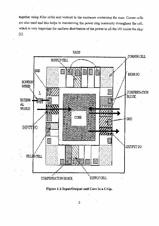
together using filler cells) and vertical to the enclosure containing the core. Corner cells
are also used and this helps in maintaining the power ring continuity throughout the cell,
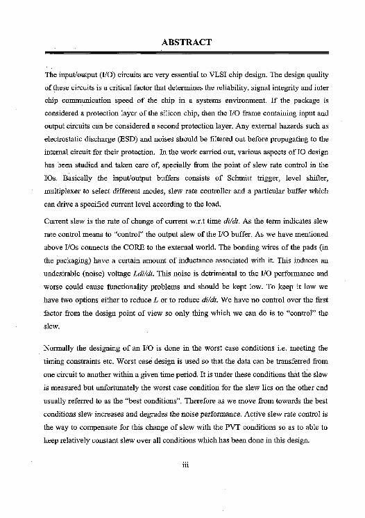
which is very important for uniform distribution of the power to all the I/O inside the chip [1].
PADS
SUPPLY CELL
L
EX ERN AL WORLD .~.
BIDIR I/O
COMPERS BLOCK
Al
FJLLF.CELL
E Pu Ito
COMPENSATION BWCK ,Y CELL
Figure 1.1-Input/Output and Core in a Chip.
2
Uniform distribution of power is necessary, as the I/Os are placed all over the periphery
and due to large distances between them there is high chance of the power getting
degraded, which means I/Os will get power in a broader range than the required one. For e.g. the actual voltage received by one buffer could be 2 V and for another one 2.5 V.
1.2 Statement of Problem
Current slew is the rate of change of current w.r.t. time di/dt. As the term indicates slew
rate control means to "control" the output slew of the 1/0 buffer. As we have mentioned above I/Os connects the CORE to the external world. The bonding wires of the pads (in
the packaging) have a certain amount of inductance associated with it. This induces an undesirable (noise) voltage Ldi/dt. This noise is detrimental to the 1/0 performance and worse could cause functionality problems and should be kept low. To keep it low we have two options either to reduce L or to reduce di/dt. We have no control over the first
factor from the design point of view so only thing which we can do is to "control" the slew.
Normally the designing of an 1/0 is done in the worst case conditions, i.e. meeting the
timing constraints. Worst case design is used so that the data can be transferred from one
circuit to another within a given time period. It is under these conditions that the slew is
measured but unfortunately the worst case condition for the slew lies on the other end usually referred to as the "best conditions". Under "best case" conditions, i.e. is to say the
temperature, process, and supply voltage states that give fastest or best performance, the CMOS output buffer will operate much too fast. Data can still be transferred within the
given time period, but the fast rate of change of current can give a very high disturbance
voltage across the inductive components of the system like the wire bonds. Therefore, as
we move from towards the best conditions slew increases and degrades the noise
performance. Active slew rate control is the way to compensate for this change of slew
with the PVT conditions so as to able to keep relatively constant slew over all conditions.
In this work, design of I/O buffer has been done keeping in view all above constraints in
3
mind such that we can get optimized performance from the I/O buffer incorporating the tradeoffs required.
1.3 Thesis Organization
This dissertation is organized into 8 chapters, of which this introduction is the first. In chapter 2 -fundamentals of I/O buffer is presented. In chapter 3, slew rate control has been discussed in detail and its application in the design has been seen. In next chapter, design
strategy of various blocks has been discussed. Specification of the I/O buffer is described
in chapter 5. Validation flow for simulation, results and discussion are presented in
chapter 6. Next chapter discusses layout issues and finally the conclusion is presented in
chapter 8.
CHAPTER 2
BASICS OF INPUT/OUTPUT BUFFER
There can be three types of buffer
• Input Buffer
• Output Buffer
• Bidirectional Buffer
2.1 Input buffer
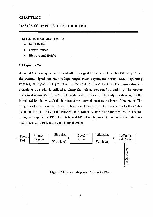
An input buffer couples the external off chip signal to the core elements of the chip. Since
the external signal can have voltage ranges much beyond the normal CMOS operating
voltages, an input ESD protection is required for these buffers. The non-destructive
breakdown of diodes is utilized to clamp the voltage between VDD and Vss. The resistor
tends to decrease the current reaching the gate of devices. The only disadvantage is the
introduced RC delay (each diode introducing a capacitance) to the input of the circuit. The
design has to be optimized if used in high speed circuits. ESD protection for buffers today
has a major role to play in the efficient chip design. After passing through the ESD block,
the signal is applied to UP buffer. A typical IT buffer (figure 2.1) may be divided into three
main stages as represented by the block diagram.
From Schmitt Signal at
Pad Trigger VDDE level
Level I Signal at Buffer To Shifter I Set Drive
VDD level H 0 0
ara' w
Figure 2.1-Block Diagram of Input Buffer.
5
2.1.1 Electrostatic Discharge (ESD) Electrostatic Discharge, in short ESD, protection is very important to save the chip from
unwanted voltage which gets developed at the pin due to some source coming in contact
with the pin. These large accumulated charges can destroy the transistor, so a mechanism is
needed which can effectively and quickly discharge this unwanted accumulated charge.
Here, again the importance of metal rings comes into picture as they discharge accumulated charges and protects the chip. Care should be taken that there are no acute angles in the
metal layers as they could be a potential areas of hotspots.
An I/P buffer couples the external off chip signal to the core elements of the chip. Since the
external signal can have voltage ranges much beyond the normal CMOS operating voltages,
an UP ESD protection is required for these buffers. Non Destructive break down of diodes is
utilized to clamp the voltages between Von and Vss. The resistor tends to decrease the
current reaching gate. But this block introduces RC delay; hence the design has to be optimized, if used in high speed circuits. There are 3 types of ESD stress models [2].
1. Human body model (HBM)
When a charged person touches packaged device, it results in discharge of the charges
accumulated at pins when his finger comes in contact with pin, with peak current in amperes
of about 100 ns duration. For HBM following factors are important:
• Human body capacitance (=100 pf)
• Charging potential (2 KV)
• Finger resistance (which limits current in circuit)=1.5 K ohm
2. Machine model
When a machine, which could be a solder iron, bonding machine, etc., comes in contact with
the pin, charges from the tip of the machine gets transfer to the pin, which results in large current.
In this model, resistance which limits peak current through circuit is much lower (25 ohm),
so RC time constant is small which leads to higher peak current (3-4 amp) as compared to HBM.
6

3. Charged device model (CDM)
In this, ESD event occurs when electrostatically charged device [i.e. charge is stored in
Device under Test (DUT), itself] is abruptly discharged to ground. CDM pulse has very fast
rise time, so protection device should turn on fast. Only thermal damage occurs in CDM
while both thermal damage and oxide rupture occur in HBM and MM.
Reason for thermal damage:
• Flow of high current through circuit results in energy dissipation which leads to
thermal damage.
Effect of Higher voltages on transistors
When 5 Von the PAD, the following effects occur:
• For NMOS
> Hot electron effect: When 5 V on the drain of NMOS, the electron coming from
the source may acquire such high energy that they can penetrate the insulating
layer of Si02 (i.e. they cross the potential barrier of Si02 layer) which will effect
the threshold voltage of transistor, in other words, will change the characteristics
of transistor.
> Gate-oxide stress potential: When 5 V comes on the PAD, the VDS of NMOS
will be 5 V which cross the stress limit (=4 V) so transistor becomes stress.
• FOR PMOS:
Flow of substrate current: In case of 5 V on the PAD, the diode formed
between the p+ of PMOS and the substrate n+ of PMOS becomes forward biased
so there will be flow of substrate current pad, without damaging the input/output
MOSFETs.
2.1.2 Schmitt Trigger
This circuit is used to generate clean pulses from a noisy input signal by providing
hysteresis. The basic principle employed for such circuit is the different switching thresholds
signals going from 'LOW' to 'HIGH' and 'HIGH' to 'LOW'
h
V. r NOISY EXTERNAL SIGNAL
V H
VIA - - ° --- ---
THRESHOLD POINT SHIFTED FOR HIGH TO LOW TRANSITION IN CASE OF HYSTERESIS
Time
L SWITCHING HYSTERESIS
SWITCHING IN ABSENCE VOUT OF HYSTERESIS
Time
Figure 2.3-Demonstration of Noise Decoupling with Hysteresis.
8

Working: We can divide the circuit into two parts, depending on whether the output is high or low. If
the output is low then M6 is on and M3 is off and we are concerned with the p-channel
portion when calculating the switching point voltages, while if the output is high, M3 is on
and M6 is off and we are concerned with the n-channel portion. Also if the output is high,
M4 and M5 are on, providing a DC path to Vu.
Lets begin our analysis of this circuit (figure 2.2), assuming that the output is high (=V0D)
and the input is low (=0 V). MOSFETs Ml and M2 are off while M3 is on. The source of
M3 floats to VDD-VTN. With Vn less than the threshold voltage of Ml, source of M3
remains at approximately VDD-VTN. As VIN is increased further, Ml begins to turn on and
the voltage, source of M3 starts to fall towards ground. As M2 starts to turn on, the output
starts to move towards ground, causing M3 to start turning off. This in turn causes the
source of M3 to fall further, turning M2 on even more. This continues until M3 is totally off
and M2 and MI are on. The positive feedback causes the switching point voltage to be very
well defined. The curve characteristic of the Schmitt Trigger is shown in figure 2.3.
2.1.3 Level Shifter
Core circuit works at a voltage of 1.2 V (typical), whereas, the signals come at higher
voltage levels so in order to apply these signals to core we need to lower the voltage level
with the help of level shifters.
Working
When input is high, NMOS-1 (figure 2.4) will be on and will try to pull down the gate of
transistor 4, hence turning it on and simultaneously transistor 2 will be off so the potential at
outl is high and hence transistor 3 is off and as transistor 1 is on, potential at OUT2 is low.
9
s
Figure 2.4-Level Shifter.
2.1.4 Input Driver
It is used to set drive, i.e. the current capability to charge the load capacitor to the desired
value in given time. Circuit is designed in such a way that the aspect ratio (W/L) which is
inversely proportional to resistance, of the transistors used in input drive section, has a value
which in turn returns the required time constant.
10
2.2 Output buffer .
These interface the outgoing signals from the core to the off chip environment. Hence
these are used to drive large capacitive loads which arise from long interconnect lines
such as clock distribution networks, high capacitance fan out and high off chip loads. The
drive capability of such a buffer should be such as to achieve the requisite rise and fall
times into a given capacitive load. Normally, the drive capability of I/O buffers is as high
as 8 mA. By driving capability, it means that the output buffer can source or sink the
specified amount of current in the worst case. Block diagram of a typical output buffer is
given in figure 2.5.
From IOpp Input Logic Pre Driver
Driver Core
Figure 2.5-Block diagram of Output Buffer.
2.2.1 Input Logic
This is connected between the core and slew rate controller. It basically comprises of
multiplexer and inverters. It works in two modes, test mode and basic operating mode
and multiplexer is there to select test or basic operating mode. The block diagram of
INPUT LOGIC block is given in figure 2.6 and its functionality based on the pins
selected is provided in table 2.1. The multiplexer is followed by the inverters to generate
two signals NIN and PIN (figure 2.6) which goes to predriver stage and drive predriver
transistors after some level shifting. Signal at NIN rises faster than PIN signal and signal
at PIN falls faster than PIN signal. This is done to ensure that the O/P driver transistors
should not have large dynamic current.
Ill
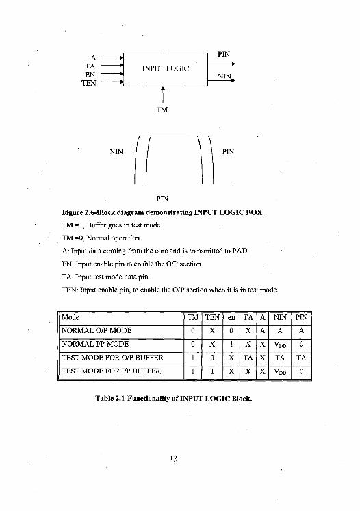
A PIN TA INPUT LOGIC EN -~ N1N TEN
TM
1
PIN
Figure 2.6-Block diagram demonstrating INPUT LOGIC BOX. TM =1, Buffer goes in test mode
TM =0, Normal operation A: Input data coming from the core and is transmitted to PAD
EN: Input enable pin to enable the O/P section
TA: Input test mode data pin
TEN: Input enable pin, to enable the O/P section when it is in test mode.
Mode TM TEN en TA A NIN PIN
NORMAL O/P MODE 0 X 0 X. A A A
NORMAL I/P MODE 0 X 1 X X VDD 0
TEST MODE FOR O/P BUFFER 1 0 X TA X TA TA
TEST MODE FOR I/P BUFFER 1 1 X X X VDD 0
Table 2.1-Functionality of INPUT LOGIC Block.
12
2.2.2 Slew Rate Controller
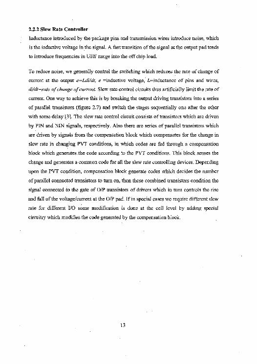
Inductance introduced by the package pins and transmission wires introduce noise, which
is the inductive voltage in the signal. A fast transition of the signal at the output pad tends
to introduce frequencies in UHF range into the off chip load.
To reduce noise, we generally control the switching which reduces the rate of change of
current at the output e=Ldi/dt, e =inductive voltage, L=inductance of pins and wires,
di/dt=rate of change of current. Slew rate control circuits thus artificially limit the rate of
current. One way to achieve this is by breaking the output driving transistors into a series
of parallel transistors (figure 2.7) and switch the stages sequentially one after the other
with some delay [3]. The slew rate control circuit consists of transistors which are driven
by PIN and NIN signals, respectively. Also there are series of parallel transistors which
are driven by signals from the compensation block which compensates for the change in
slew rate in changing PVT conditions, in which codes are fed through a compensation
block which generates the code according to the PVT conditions. This block senses the
change and generates a common code for all the slew rate controlling devices. Depending
upon the PVT condition, compensation block generate codes which decides the number
of parallel connected transistors to turn on, then these combined transistors condition the
signal connected to the gate of O/P transistors of drivers which in turn controls the rise
and fall of the voltage/current at the O/P pad. If in special cases we require different slew
rate for different I/O some modification is done at the cell level by adding special
circuitry which modifies the code generated by the compensation block.
13
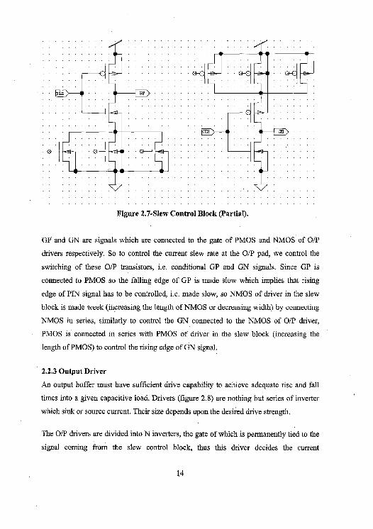
GP and GN are signals which are connected to the gate of PMOS and NMOS of O/P
drivers respectively. So to control the current slew rate at the O/P pad, we control the
switching of these O/P transistors, i.e. conditional GP and GN signals. Since GP is
connected to PMOS so the falling edge of GP is made slow which implies that rising
edge of PIN signal has to be controlled, i.e. made slow, so NMOS of driver in the slew
block is made week (increasing the length of NMOS or decreasing width) by connecting
NMOS in series, similarly to control the GN connected to the NMOS of O/P driver,
PMOS is connected in series with PMOS of driver in the slew block (increasing the
length of PMOS) to control the rising edge of GN signal.
2.2.3 Output Driver
An output buffer must have sufficient drive capability to achieve adequate rise and fall
times into a given capacitive load. Drivers (figure 2.8) are nothing but series of inverter
which sink or source current. Their size depends upon the desired drive strength.
The O/P drivers are divided into N inverters, the gate of which is permanently tied to the
signal coming from the slew control block, thus this driver decides the current
14
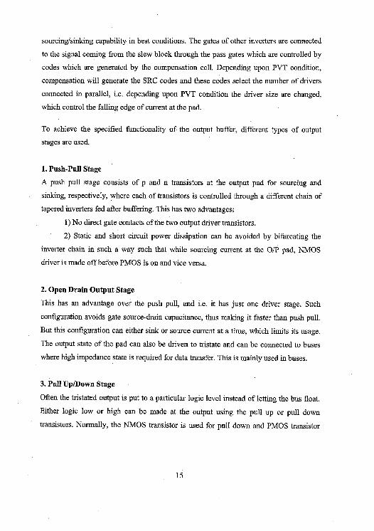
sourcing/sinking capability in best conditions. The gates of other inverters are connected
to the signal coming from the slew block through the pass gates which are controlled by
codes which are generated by the compensation cell. Depending upon PVT condition,
compensation will generate the SRC codes and these codes select the number of drivers
connected in parallel, i.e. depending upon PVT condition the driver size are changed,
which control the falling edge of current at the pad.
To achieve the specified functionality of the output buffer, different types of output
stages are used.
1. Push-Pull Stage
A push pull stage consists of p and n transistors at the output pad for sourcing and
sinking, respectively, where each of transistors is controlled through a different chain of
tapered inverters fed after buffering. This has two advantages:
1) No direct gate contacts of the two output driver transistors.
2) Static and short circuit power dissipation can be avoided by bifurcating the
inverter chain in such a way such that while sourcing current at the O/P pad, NMOS
driver is made off before PMOS is on and vice versa.
2. Open Drain Output Stage
This has an advantage over the push pull, and i.e. it has just one driver stage. Such
configuration avoids gate source-drain capacitance, thus making it faster than push pull.
But this configuration can either sink or source current at a time, which limits its usage.
The output state of the pad can also be driven to tristate and can be connected to buses
where high impedance state is required for data transfer. This is mainly used in buses.
3. Pull Up/Down Stage
Often the tristated output is put to a particular logic level instead of letting the bus float.
Either logic low or high can be made at the output using the pull up or pull down
transistors. Normally, the NMOS transistor is used for pull down and PMOS transistor
15
for pull up. But the strength of the transistor is so chosen that when a logic level appears
at the output from core, it must overcome the pulling up or pulling down action.
PAD
Figure 2.8-Output Drivers.
2.3 Bidirectional Buffer
This contains both input and output buffers and signal can enter as well as leave the core.
Advantage of input buffers or output buffers over bidirectional buffers (figure 2.9) is that
due to smaller circuitry in them, there is less leakage current. So an input output buffer
contains both of the input and output buffer integrated in a single circuitry. Design of I/O
buffer requires the design issues to be taken into consideration for both the input and
output section.
16
Pull up/Pull Down
To Input ESD
Core VDDNDDE VDDE
EN Input logic Level shifter and Output TN Predriver Stage TM I Pw
PAD
Gnd vnwvnae Gnde
Figure 2.9-Block Diagram of Input/Output Buffer.
17
CHAPTER 3
SLEW RATE CONTROL
3.1 Introduction Current slew is the rate of change of current w.r.t. time di/dt. As the term indicates slew rate
control means to "control" the output slew of the I/O buffer. As we have mentioned above
I/Os connects the CORE to the external world. The bonding .wires of the pads (in the
packaging) have a certain amount of inductance associated with it. This induces an
undesirable (noise) voltage Ldi/dt. This noise is detrimental to the 1/0 performance and
worse could cause functionality problems and should be kept low. To keep it low we have
two options either to reduce L or to reduce di/dt. We have no control over the first factor
from the design point of view so only thing that we can do is to "control" the slew.
Normally the designing of an 1/0 is done in the worst case conditions, i.e. meeting the
timing constraints, etc. Worst case design is used so that the data can be transferred from
one circuit to another within a given time period. It is under these conditions that the slew is
measured but unfortunately the worst case condition for the slew lies on the other end
usually referred to as the "best conditions". Therefore, as we move from towards the best
conditions, slew increases and degrades the noise performance. Active slew rate control is
the way to compensate for this change of slew with the PVT conditions so as to able to keep
relatively constant slew over all conditions.
3.2 Basic Principle
The basic principle used in this design of SRC buffer is dependence of output current slew
on the width of transistors in the predriver. The general mathematics to understand the
concept is done here for a simple case with some assumptions.
18
M' c
Figure 3.1-A simplified Predriver Stage with a Step Voltage at the Input.
At t=0, V; (figure 3.1) instantaneously changes from 0 to VDn (also capacitor is initially
charted to VDD at t=0). MOSFET Ml gets on in saturation mode as VDSI>VGS1'Vti.
MOSFET M2 gets OFF as VsG2<V0. Since voltage across a capacitor can't change
instantaneously, capacitor C discharges through Ml. Now as MOSFET Ml is in saturation,
/3 _v)2 7o = ~ly2L " . Where ,6= [CS C_
also, z
I lqW = —i(t) 2L
and so di
v0 (t) _ . f i(t)dt
Vl)2 dt
C 2L
-/3W J v0 (t)
_ 2CL (VDO — V,1)
z dt
v° (t) _ —~ (VDD —V 1 )z ,t+Const 2CL
19
At t = 0, vo (t) = VDD
—PW t v0(t)= 2CL '.;(VDD
— V l ) t±VDD '
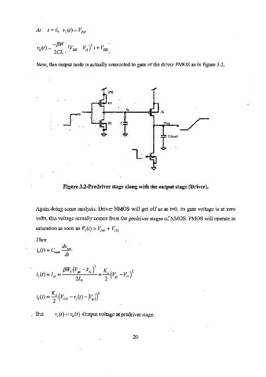
Now, this output node is actually connected to gate of the driver PMOS as in figure 3.2.
Figure 3.2-Predriver stage along with the output stage (Driver).
Again doing some analysis, Driver NMOS will get off as at t=0, its gate voltage is at zero
volts, this voltage actually comes from the predriver stages of NMOS. PMOS will operate in
saturation as soon as V,. (t) > VDD + IV, Then
dvo , to (t) = Ctoaa dt
— K'IVgs—V1„ 2
oO D 2L3 2 I
io (t)= Z3 (VDD —v(t) —IV,, I)z
But v, (t) = vo (t) Output voltage at predriver stage.
20

Hence
1/V
z z `DD - v1
l / t VDD v }
12
i0( t ) - L 1 VDD + `VDD -tLJ 2t4VODi_ PI(
Differentiating above with respect to time gives us the current slew rate at the output node.
di (t) K K z
dt 2 Z VD°+(VDD —V l )
z t—VDD`_
— li nl 0+(VD1—V1. 0 i -0
di, (t) _ K3 2 { V + K` (V V )2 t V _ I V { K' (V VR) ]
dt Z OD ZG DD A DD .per p 2C OD J
dio(t) — KIK3 JV + K` ' V V ~z t ~ J(V
V V)2}dt 2C 1 DD 2C . DD — n DD"DD "
z 1 r 1 dl~~t)- VDD 21C3+ 41C 3 : ~I~VDD -V11 Yt VD 21C3 I~P }
(VDD -~I ~z J
from above, we can see that
C is the parasitic capacitance at node gate of driver
dio (t)K
W3 dt a ' L3
and most importantly
z dio (t) a K 2 _( W
dt L,)
21

Hence, from above it is clear that adjusting the width of transistors of predriver stage can
control the current slew rate. This concept is exploited in design of slew rate control in the
I/O buffer.
3.3 Application of the Principle in design
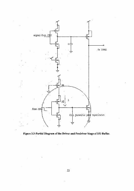
Consider the figure 3.3; it is a partial diagram of the driver and predriver stage of I/O buffer.
Concept developed in the previous section is exploited here to make the design. Consider the
encircled part of the circuit. This is enabled when a HIGH-to-LOW signal comes from the
core. When the signal from the core becomes low, both Ml and M2 get ON and they drive
the NMOS portion of Output Driver.
The slew is directly proportional to current through M2 and inversely proportional to C2 (C
is parasitic gate capacitance). But gate capacitance is process dependent, so maximum. Slew
is controlled by controlling the current I which in turn is controlled by adjusting the sizes of
Ml and M2. Generally we keep the size of M2 as constant and hence the maximum slew can
be fixed by adjusting the W/L of Ml. For I/Os without active slew rate control, the size of
Ml is fixed in accordance with a given maximum slew rate for typical case (Typical PVT).
Whereas, in active slew rate controlled I/Os, W/L of Ml is variable and changed according
to the variation in PVT conditions. This is achieved by implementing Ml as a combination
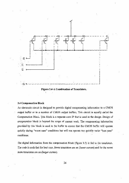
of transistors whose gates are driven by control signals from another core I/P called
compensation block. As shown in figure 3.4, GO, Gl, G2 ... Gn are control signals from
compensation block to the 110 buffer.
22
•fY~
Figure 3.3-Partial Diagram of the Driver and Predriver Stage of I/O Buffer.
23
ei
Figure 3.4-A,Combination of Transistors.
3.4 Compensation Block
An electronic circuit is designed to provide digital compensating information to a CMOS
output buffer or to a number of CMOS output buffers. This circuit is usually called the
Compensation Block. This block is a separate core IP that is used in the design. Design of
compensation block is beyond the scope of current work. The compensating information
provided by this block is used in the buffer to ensure that the CMOS buffer will operate
quickly during "worst case" conditions but will not operate too quickly under "best case"
conditions.
The digital information from the compensation block (figure 3.5) is fed to the transistors.
The code is such that for best case, fewer transistors are on (lesser current) and for the worst
more transistors are on (larger current).
24
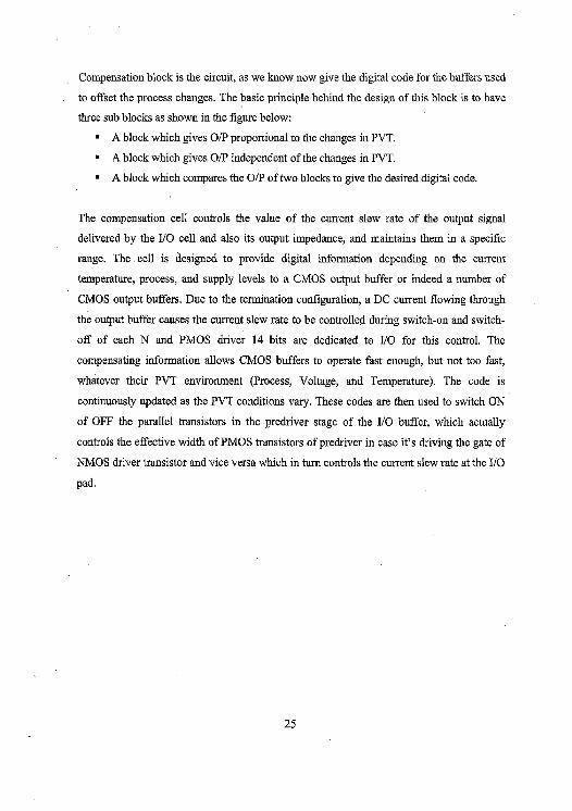
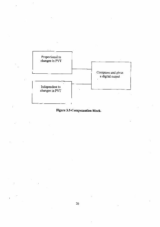
Compensation block is the circuit, as we know now give the digital code for the buffers used
to offset the process changes. The basic principle behind the design of this block is to have
three sub blocks as shown in the figure below:
• A block which gives O/P proportional to the changes in PVT.
• A block which gives O/P independent of the changes in PVT.
■ A block which compares the O/P of two blocks to give the desired digital code.
The compensation cell controls the value of the current slew rate of the output signal
delivered by the 1/0 cell and also its output impedance, and maintains them in a specific
range. The . cell is designed to provide digital information depending on the current
temperature, process, and supply levels to a CMOS output buffer or indeed a number of
CMOS output buffers. Due to the termination configuration, a DC current flowing through
the output buffer causes the current slew rate to be controlled during switch-on and switch-
off of each N and PMOS driver 14 bits are dedicated to I/O for this control. The
compensating information allows CMOS buffers to operate fast enough, but not too fast,
whatever their PVT environment (Process, Voltage, and Temperature). The code is
continuously updated as the PVT conditions vary. These codes are then used to switch ON
of OFF the parallel transistors in the predriver stage of the I/O buffer, which actually
controls the effective width of PMOS transistors of predriver in case it's driving the gate of
NMOS driver transistor and vice versa which in turn controls the current slew rate at the I/O
pad.
25
Proportional to changes in PVT
Compares and gives a digital output
Independent to changes in PVT
Figure 3.5-Compensation Block.
26
CHAPTER 4
Design Strategy
In the design of Input/Output buffers, there are some critical aspects which have to be taken
into consideration at various design levels. Main focus will be on designing the circuit for
hysteresis, ESD protection circuit, Driver (simple inverter) and Current buffer with Xma
driving capability (where X is any number in suitable range) and aspects regarding active
slew rate control will also be discussed.
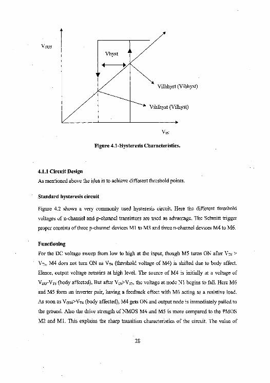
4.1 Hysteresis Hysteresis is often required in input buffers to decouple the noisy external signal from the
core circuitry of the chip. For a noisy external signal we desire that the buffer doesn't switch
its state due to noise. We should have a margin for the noise considerations as shown in the
figure 4.1. As long as the signal doesn't go below Vilhyst, the O/P doesn't change. So you
have a margin of Vihhyst-Vilhyst. Normally, without hysteresis it will start changing as
soon as the voltage goes below Vihhyst (in this case).
The basic principle employed for such circuit is the different switching thresholds for input
signals from low to high and high to low transitions, i.e. when we apply low voltage to the
I/P and ramp it up to the high level the threshold point comes say at a point VIN=Vilhyst.
Similarly when we apply a high voltage at I/P and decrease it, the threshold point comes at
point VIN=Vihlhyst. We need these points to be different such that Vilhhyst>Vihlhyst as
shown in the figure 4.1 below.
27
VOUT
Vihhyst)
hyst)
VIN
Figure 4.1-Hysteresis Characteristics.
4.1.1 Circuit Design
As mentioned above the idea is to achieve different threshold points.
Standard hysteresis circuit
Figure 4.2 shows a very commonly used hysteresis circuit. Here the different threshold
voltages of n-channel and p-channel transistors are used as advantage. The Schmitt trigger
proper consists of three p-channel devices Ml to M3 and three n-channel devices M4 to M6.
Functioning
For the DC voltage sweep from low to high at the input, though M5 turns ON after VIN >
VT5, M4 does not turn ON as VT4 (threshold voltage of M4) is shifted due to body affect.
Hence, output voltage remains at high level. The source of M4 is initially at a voltage of
VDD-VT6 (body affected). But after VIN>VT5, the voltage at node Ni begins to fall. Here M6
and M5 form an inverter pair, having a feedback effect with M6 acting as a resistive load.
As soon as VGS4>VT4 (body affected), M4 gets ON and output node is immediately pulled to
the ground. Also the drive strength of NMOS M4 and M5 is more compared to the PMOS
M2 and MI. This explains the sharp transition characteristics of the circuit. The value of
28
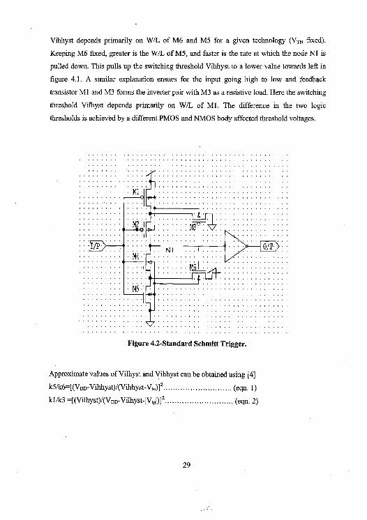
Vihhyst depends primarily on W/L of M6 and M5 for a given technology (Vm fixed).
Keeping M6 fixed, greater is the W/L of M5, and faster is the rate at which the node Ni is
pulled down. This pulls up the switching threshold Vihhyst to a lower value towards left in
figure 4.1. A similar explanation ensues for the input going high to low and feedback
transistor Ml and M3 forms the inverter pair with M3 as a resistive load. Here the switching
threshold Vilhyst depends primarily on W/L of M1. The difference in the two logic
thresholds is achieved by a different PMOS and NMOS body affected threshold voltages.
Figure 4.2-Standard Schmitt Trigger.
Approximate values of Vilhyst and Vihhyst can be obtained using [4]
k5/k6=[(VDD-Vihhyst)/(Vihhyst-Vtn)]Z ............................ (eqn. 1)
kl/k3 =[(Vilhyst)/(VDD Vilhyst-JV)]Z ............................ (eqn. 2)
29
4.2 Drive strength
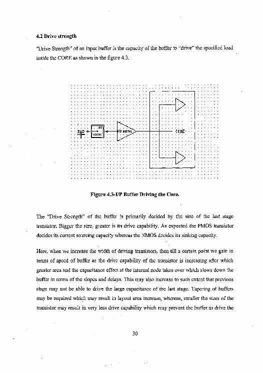
"Drive Strength" of an input buffer is the capacity of the buffer to "drive" the specified load
inside the CORE as shown in the figure 4.3.
Figure 4.3-TIP Buffer Driving the Core.
The "Drive Strength" of the buffer is primarily decided by the size of the last stage
transistor. Bigger the size, greater is its drive capability. As expected the PMOS transistor
decides its current sourcing capacity whereas the NMOS decides its sinking capacity.
Here, when we increase the width of driving transistors, then till a certain point we gain in
terms , of speed of buffer as the drive capability of the transistor is increasing after which
greater area and the capacitance effect at the internal node takes over which slows down the
buffer in terms of the slopes and delays. This may also increase to such extent that previous
stage may not be able to drive the large capacitance of the last stage. Tapering of buffers
may be required which may result in layout area increase, whereas, smaller the sizes of the
transistor may result in very less drive capability which may prevent the buffer to drive the
30
required number of gates in the CORE. Normal drive which is called as X4 drive is
characterized with internal loads up to 80 standard loads, i.e. 0.72 pF. High drive which is
equivalent to an X16 drive in the standard digital library is characterized with loads up to
316 standard loads, i.e. 2.84 pF [5].
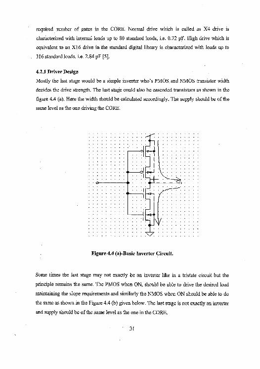
4.2.1 Driver Design
Mostly the last stage would be a simple inverter who's PMOS and NMOS transistor width
decides the drive strength. The last stage could also be cascoded transistors as shown in the
figure 4.4 (a). Here the width should be calculated accordingly. The supply should be of the
same level as the one driving the CORE.
LftLiHHH
T1.T1 Figure 4.4 (a)-Basic Inverter Circuit.
Some times the last stage may not exactly be an inverter like in a tristate circuit but the
principle remains the same. The PMOS when ON, should be able to drive the desired load
maintaining the slope requirements and similarly the NMOS when ON should be able to do
the same as shown in the Figure 4.4 (b) given below. The last stage is not exactly an inverter
and supply should be of the same level as the one in the CORE.
31
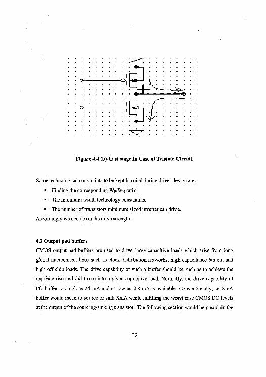
Figure 4.4 (b)-Last stage in Case of Tristate Circuit.
Some technological constraints to be kept in mind during driver design are:
• Finding the corresponding Wp/WN ratio.
• The minimum width technology constraints.
• The number of transistors minimum sized inverter can drive.
Accordingly we decide on the drive strength.
4.3 Output pad buffers
CMOS output pad buffers are used to drive large capacitive loads which arise from long
global interconnect lines such as clock distribution networks, high capacitance fan out and
high off chip loads. The drive capability of such a buffer should be such as to achieve the
requisite rise and fall times into a given capacitive load. Normally, the drive capability of
I/O buffers as high as 24 mA and as low as 0.8 mA is available. Conventionally, an XmA
buffer would mean to source or sink XmA while fulfilling the worst case CMOS DC levels
at the output of the sourcing/sinking transistor. The following section would help explain the
32
meaning of an XmA buffer and gives the analytical design equations for designing such an
output transistor drivers.
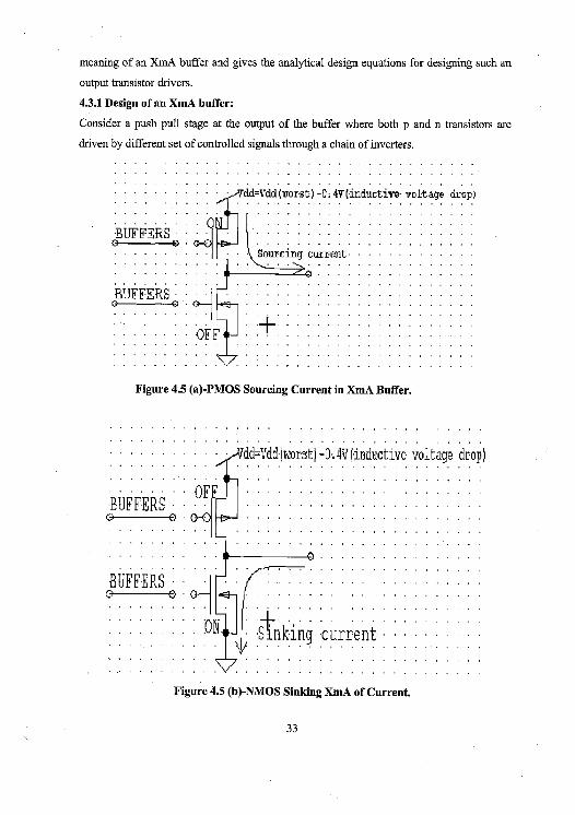
4.3.1 Design of an XmA buffer:
Consider a push pull stage at the output of the buffer where both p and n transistors are
driven by different set of controlled signals through a chain of inverters. .................................... .............................. . ....................................
. • . . dd=Vdd{Tsnrst)-0 4V(•inductive-voItage drop)
BUFFERS : ....... . ... . ... . . 0 0. ......................
• . . . . . • Sourcing current. . . . . . . . . ............ .. ... ................. .......... >0.. . ........... ........................ BUFFERS .. i I . .. ... .... ... ... .. .... . .......... . ....................... ...... ............. ........OFF ......................
Figure 4.5 (a)-PMOS Sourcing Current in XmA Buffer.
........................
........................
VddhVdd(worst)-O.4U(.inductive voltage drop)
Figure 4.5 (b)-NMOS Sinking XmA of Current.
33
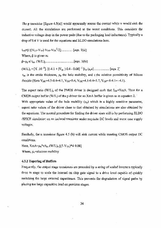
The p transistor [figure 4.5(a)] would apparently source the current while n would sink the
current. All the simulations are performed at the worst conditions. This considers the
inductive voltage drop in the power pads (due to the packaging lead inductance). Typically a
drop of 0.4 V is used for the equations and ELDO simulations here.
IDS= l [(VGS-VTP) VDS-VDS2/2] .............. [eqn. I(a)]
Where, (0 is given as
13=µp cl tax. (W/L)p .................................. [eqn. 1(b)]
(W/L)P = [X .10 -3]. [(-4.1 + IV,, ) 0.4 - 0.08] -1 [tox/µPE] ................... [eqn. 2]
to,, is the oxide thickness, µP the hole mobility, and s the relative permittivity of Silicon
dioxide (Here VoD=4.5-0.4=4.1, VDS=0.4, Von=4.1-0.4=3.7, VGS= 0-4.1= -4.1).
The aspect ratio (W/L)p of the PMOS driver is designed such that IDs=XmA. Thus for a
CMOS output buffer (WIL) of the p driver for an XmA buffer is given as in equation 2.
With appropriate value of the hole mobility (µp) which is a highly sensitive parameter,
aspect ratio values of the driver close to that obtained by simulations are also obtained by
the equations. The normal procedure for finding the driver sizes still is by performing ELDO
/SPICE simulation on an isolated transistor under requisite DC levels and worst case supply
voltages.
Similarly, the n transistor figure 4.5 (b) will sink current while meeting CMOS output DC
conditions.
Here, XmA=µ„*s/tox (W/L)n [(5-VTN)*4-0.08]
Where, i, electron mobility
4.3.2 Tapering of Buffers
Frequently, the output stage transistors are preceded by a string of scaled inverters typically
three in stage to scale the internal on chip gate signal to a drive level capable of quickly
switching the large external capacitance. This prevents the degradation of signal paths by
placing too large capacitive load on previous stages.
34
The optimization to be achieved in such scaling is to minimize the delay between the input
and output while maintaining the area and the power dissipation. A basic derivation of
tapering factor in [6] has shown the factor to vary between 3 to 10. A series of advanced
works has appeared recently in journals. The work [7] gives an accurate expression of this
factor taking into account the short circuit current power consumption. Undoubtedly, the
tapering of buffers for optimization to meet constraints such as area, power, and speed has
come to occupy a degree of importance in buffer design. An extensive deal on this topic is
certainly out of scope of the present work.
4.3.3 Different output stages
Often a plain inverter stage at the output of buffers is avoided. The miller capacitance
formed between the gates and the source-drain diffusion of p and n transistors can result in
oscillations at the output in series with the lead inductance. The short circuit power
dissipation is also a possibility in such a configuration. These limitations have given rise to
several types of output stages. Below is explained some of the widely used configurations
with their relative merits.
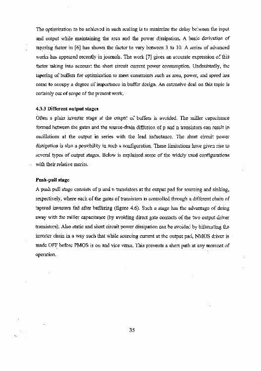
Push-pull stage
A push pull stage consists of p and n transistors at the output pad for sourcing and sinking,
respectively, where each of the gates of transistors is controlled through a different chain of
tapered inverters fed after buffering (figure 4.6). Such a stage has the advantage of doing
away with the miller capacitance (by avoiding direct gate contacts of the two output driver
transistors). Also static and short circuit power dissipation can be avoided by bifurcating the
inverter chain in a way such that while sourcing current at the output pad, NMOS driver is
made OFF before PMOS is on and vice versa. This prevents a short path at any moment of
operation.
35
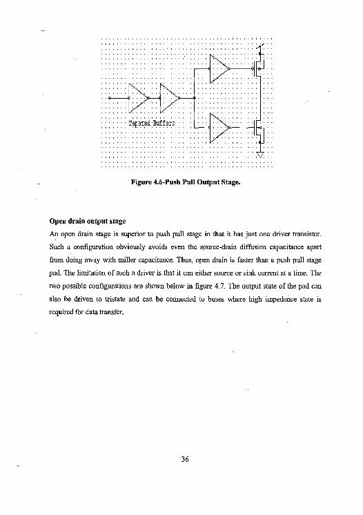
Figure 4.6-Push, Pull Output Stage.
Open drain output stage
An open drain stage is superior to push pull stage in that it has just one driver transistor.
Such a configuration obviously avoids even the source-drain diffusion capacitance apart
from doing away with miller capacitance. Thus, open drain is faster than a push pull stage
pad. The limitation of such a driver is that it can either source or sink current at a time. The
two possible configurations are shown below in figure 4.7. The output state of the pad can
also be driven to tristate and can be connected to buses where high impedance state is
required for data transfer.
36
vP orn H H
L Z
Figure 4.7-Open Drain Output Stage.
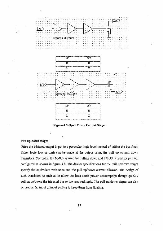
Pull up/down stages
Often the tristated output is put to a particular logic level instead of letting the bus float.
Either logic low or high can be made at the output using the pull up or pull down
transistors. Normally, the NMOS is used for pulling down and PMOS is used for pull up,
configured as shown in figure 4.8. The design specifications for the pull up/down stages
specify the equivalent resistance and the pull up/down current allowed. The design of
such transistors is such as to allow the least static power consumption though quickly
pulling up/down the tristated bus to the required logic. The pull up/down stages can also
be used at the input of input buffers to keep them from floating.
37
Figure 4.8-Output/Input Pull-Up Pull-Down Transistors.
4.4 Slew Rate Control
We had already discussed the slew rate control in detail in the chapter 3 of the thesis.
This section describes how the compensation circuit and output buffer work together.
The output current slew rate can be very high if both the output transistors switch at the
same time. In all 1/Os structures (compensated and non compensated) direct supply-to-
ground current flow is avoided by delaying one output transistor switch from the other.
Both output transistors never conduct at the same time. Finally, the output current to be
controlled is the current flowing between the load and the power supply (or ground). This
is performed by the compensation structure.
In this compensated I/O structure as shown in figure 4.9, the switch-on (rising and
falling) currents slew rates are limited by means of controlling the rising time of the
NMOS driving signal and the falling time of PMOS driving signal, i.e. we can see two
different circuits dedicated to the two output transistor driving, that is unusual in standard
inverters. Positive slew rate (during 0>1 transition) is controlled by slowing the output
PMOS switch, and negative slew rate (during 1>0 transition) is controlled by slowing the
output NMOS transistor switch.
38
C t?ent
n -> 9?—, rzse can£ea1 M
Figure: 4.9-Compensated Output Buffer.
How an output transistor switch can be slowed? This is done by means of a driving
inverter. The signal PIN arrives at the inverter driving the PMOS and NIN arrives at the
inverter driving the NMOS. NIN rises faster than PIN and falls after PIN as in figure 2.6.
As a result, the switching time of each output transistor towards its ON state is delayed
from the switching time of the opposite transistor towards its OFF state. Secondly, each
output transistor current slew rate depends on its gate voltage rising (or falling) time and
39
this voltage rising time depends on the current provided by the driving inverter to fill-in the output transistor gate capacitance. So we have to control the driving inverter output
current with regards to the PVT conditions. This is done by means of the Slew-rate
Control Block (SCB), which provides a limited biasing current to the driving inverter,
controlled by the compensation code as discussed in the chapter 4.
Figure 4.10-Driving Signals of the Two Output Transistors.
Figure 4.11-Slew Rate Control Block 1.
40
Figure 4.10 shows the two output transistors driving signals. It can be seen that the falling
slope of the P driving voltage (INP) is gentled by the Slew-rate Control Block 1 (SCB1).
The opposite phenomena occur on the output NMOS driving signal. The Slew rate
Control Block SCB 1 is used to limit the rate at which the gate voltage of P1 falls towards
ground. Figure 4.11 shows the Slew rate Control Block SCB1. This circuit includes
NMOS transistors connected to ground switched by the inverted digital compensation
code. Thus under worst conditions when the digital compensation code is "0000000, all
of the NMOS transistors are turned on. As a result, under worst conditions the gate
voltage of transistor Pl is quickly pulled down by 8 parallel transistors. Under maximum
conditions, when the digital compensation code is "1111111" all of the NMOS transistors
are turned off except one of them which is always connected to the supply. Thus, under
maximum conditions the gate of transistor P1 is slowly pulled down by only one
transistor. The Slew rate Control Block 2 is used to limit the rate at which the gate
voltage of output transistor NI rises towards the supply voltage. It includes PMOS
transistors connected to the supply and switched by the digital code (not inverted).
Transistors of the Slew rate Control Block are wide and long so that they remain
insensitive in size to process variations.
4.5 Input ESD Protection
An input buffer couples the external off chip signal to the core elements of the chip.
Since the external signal can have voltage ranges much beyond the normal CMOS
operating voltages, an input ESD protection is required for these buffers. The non-
destructive breakdown of diodes is utilized to clamp the voltage between VDD and Vss•
The resistor tends to decrease the current reaching the gate of devices. Figure 4.12 shows
the circuit to achieve the diode clamping [8]. The only disadvantage is the introduced RC
delay (each diode introducing a capacitance) to the input of the circuit. The design has to
be optimized if used in high speed circuits.
41
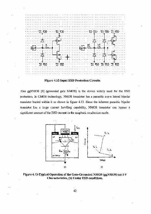
Figure 4.12-Input ESD Protection Circuits.
Also ggNMOS [8] (grounded gate NMOS) is the device widely used for the ESD
protection. In CMOS technology, NMOS transistor has a parasitic n-p-n lateral bipolar
transistor buried within it as shown in figure 4.13. Since the inherent parasitic bipolar
transistor has a large current handling capability, NMOS transistor can bypass a
significant amount of the ESD current in the snapback conduction mode.
boh a_n
(a)
Figure 4.13-Typical Operation of the Gate-Grounded NMOS (ggNMOS) (a) IN Characteristics, (b) Under ESD conditions.
42

where Ism, is the avalanche generation current, Is„b is the substrate current, Ic is the
collector current, lb is the base.current (i.e. Ib=Inert lb), Vt1 (It,) is the triggering voltage
(current), Vh (Ih) is the holding voltage (current), and V,2 (It2) is the second breakdown
triggering voltage (current).
ESD protection for buffers today has a major role to play in the efficient chip design. A
full level discussion on this issue has been left out of the present work for terseness sake
and as a course for future work.
43
CHAPTER 5
Specification of bidirectional buffer
The design strategy of designing the bidirectional buffer has been discussed in previous
chapters. Keeping those design strategies into mind a bidirectional buffer with the following
specifications has been designed.
5.1 Electrical specifications
Table 5.1 gives the electrical specification of the bidirectional buffer.
Parameter Minimum Typical Maximum Unit VDD Core power supply 0.9 1.0 1.1 V
voltage
VDDE2V5 2.5 V 110 power 2.2 2.5 2.7 V supply voltage
Tj Operating junction -40 25 125 °C temperature
Table 5.1— Electrical Specifications of Bidirectional Buffer.
5.2 I/O specifications for 2.5 V BIDIR
The 2.5 V I/Os comply to the JEDEC standard. Table 5.2 gives the DC input specifications
for the 1/0 buffer and table 5.2 gives DC output specifications.
Parameter Minimum Maximum Unit Vii Low level input 0.7 V
voltage
Vih High level input 1.7 V voltage
Vhyst Schmitt trigger 300 600 mV hysteresis
Table 5.2-DC Input Specification (2.2 V< VDDE2vs<2.7 V).
44
Parameter Minimum Maximum Unit Vol Low level O/P 0.2 V
voltage
Voh High level O/P V0DE2v5-0.2 V voltage
Table 5.3-DC Output Specifications (2.2 V< VDDE2vs<2•7 V)
5.3 Buffers description (functionality)
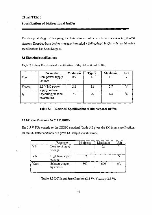
5.3.1 Bidirectional buffer
A typical diagram of bidirectional 1/0 is given in figure 5.1 and table 5.4 gives its modes of
operation.
Figure 5.1-Bi-Directional I/O.
EN Function
0 Output buffer plus copy of A on ZI. The I/P signal arrives on A, the cell drives
I/O and ZI with I/O=ZI=A
1 Input buffer. The input signal arrives on I/O, the cell drives ZI with ZI=I/O. A is
not used
Table 5.4-Modes of Operation of a Normal Bidirectional Buffer.
45
5.3.2 Output stage
• The rating of output buffers (which is 2 mA) is a DC specification. This is the
current a buffer can source/sink within VOH and VOL specifications, in worst
case conditions. The maximum output current during output switching is much
higher.
• The primary goal of the slew rate control circuitry is to reduce the SLOPE of the
CURRENT flowing to/from the load.
5.3.3 Modes of operation for 2.5 V I/O
Normal operation (NORMAL INPUT/OUTPUT MODE)
• If the pin EN is LOW for a bidirectional buffer then the buffer is in output mode,
and can drive out a 2.5 V signal.
• If the pin EN is HIGH (1.0 V) for a bidirectional buffer then the buffer is in input
mode, and can receive a 2.5 V signal.
IDDO Test Model
• For IDDQ test there should be no dissipation in I/Os.
46
CHAPTER 6
Validation Flow, Results and Discussion
Usually, an I/O library consists of
■ Level converter
■ Schmitt trigger
■ Multiplexer
■ Slew rate controller
There may be other blocks to which may be designed as per according to specifications and
their necessity. After the completion of design, there is a necessity of regression of that
particular library. Regression is nothing but to simulate the library to check the values of the
circuit are coming in specifications or not. Before discussing the regression of the library, let
us discuss the flow of tools which are used in regression of libraries.
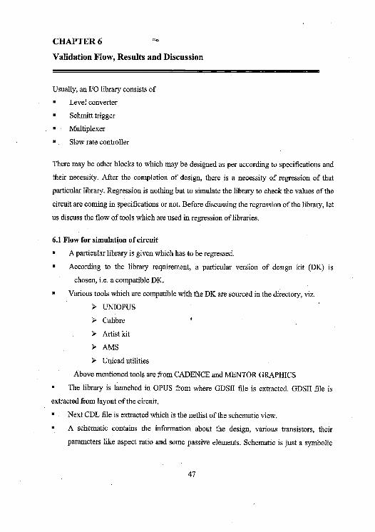
6.1 Flow for simulation of circuit
■ A particular library is given which has to be regressed.
■ According to the library requirement, a particular version of design kit (DK) is
chosen, i.e. a compatible DK.
■ Various tools which are compatible with the DK are sourced in the directory, viz.
> UNIOPUS
➢ Calibre
> Artist kit
> AMS
> Unicad utilities
• Above mentioned tools are from CADENCE and MENTOR GRAPHICS
■ The library is launched in OPUS from where GDSII file is extracted. GDSII file is
extracted from layout of the circuit.
■ Next CDL file is extracted which is the netlist of the schematic view.
■ A schematic contains the information about the design, various transistors, their
parameters like aspect ratio and some passive elements. Schematic is just a symbolic
47
representation of the circuit in design. Actual physical data that goes into chip is
layout. Virtuoso Layout Editor (OPUS) is used to make layouts. The schematic
(contains all the information and simulations) run on the netlist to check whether the
results are in desired range and with the help of the schematic, layouts are designed.
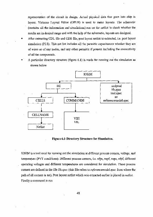
• After extracting CDL file and GDS file, post layout netlist is extracted, i.e. post layout
simulation (PLS). This net list includes all the parasitic capacitances whether they are
of wires or of any nodes, and any other parasitic if present including the connectivity
of all the components.
• A particular directory structure (figure 6.1) is made for running out the simulation as
shown below
IOSIM
BE .ucdprod lib.spec
tool. spec so
CELLS COMMANDS referencemodel.spec
CELLNAME I VIH VIL
I Netlist
Figure 6.1-Directory Structure for Simulation.
IOSIM is a tool used for running out the simulation at different process comers, voltage, and
temperature (PVT conditions). Different process comers, i.e. nfps, nspf, nsps, nfpf different
operating voltages and different temperatures are considered for simulation. These process
corners are defined in the file lib.spec (this file refers to referencemode1.spec from where the
path of all corners is set). Post layout netlist which was extracted earlier is placed in netlist.
Finally a command is run
48
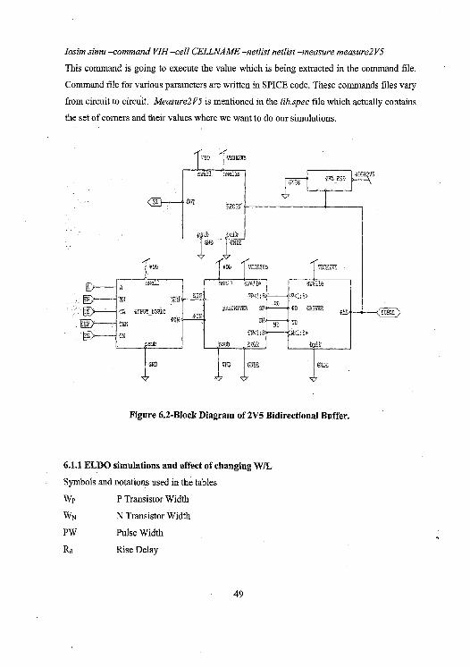
losim simu —command VIH —cell CELLNAME —netlist netlist —measure measure2 V5
This command is going to execute the value which is being extracted in the command file.
Command file for various parameters are written in SPICE code. These commands files vary
from circuit to circuit. Measure2V5 is mentioned in the lib.spec file which actually contains
the set of corners and their values where we want to do our simulations.
Figure 6.2-Block Diagram of 2V5 Bidirectional Buffer.
6.1.1 ELDO simulations and effect of changing W/L
Symbols and notations used in the tables
Wp P Transistor Width
WN N Transistor Width
PW Pulse Width
Rd Rise Delay
49

Fd Fall Delay
R, Rise Time
Ft Fall Time
Vti1 Maximum Output Voltage
vm Minimum Output Voltage
Ise Current Sourcing Capability
Is„ Current Sinking Capability
Sf Falling Edge Slew Rate
Sr Rising Edge Slew Rate
+ Increase in the value
++ Large increase in the value
- Decrease in the value
- - Large decrease in the value
* No change in the value
< Slight increase in the value
> Slight decrease in the value
Observed values at different widths of transistors are compared with values obtained at the
nonnal width of transistors
WP WN PW Rd Fd Rc Ft VM VM Isr Isn Sf S,
+ * + - < - > + > + * * +
++ * ++ — < -- > + > ++ * * *1-
* + - * - * -
- -
--
* - * > * + + * * _-
* -- * - * ++ ++ *
+ + < - - - -- + - + + + +
++ ++ < -- -- -- -- + -- ++ ++ ++ ++
Table 6.1-Results obtained while changing the Width of Transistors in the Driver
Block of the Bidirectional Buffer I~,,,
50 --~
44 s

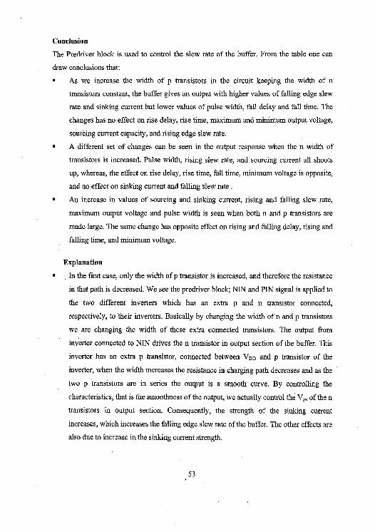
Conclusion
■ When width of only p transistors are increased; pulse width, rising edge slew rate,
maximum output voltage, and current sourcing capability of the buffer increases while
rise delay and rise time decreases.
■ When width of only n transistors are increased; current sinking capacity and falling
edge slew rate increases but pulse width, fall delay, fall time, and minimum output
voltage decreases.
■ When width of both p and n are increased; the output response has mixed
characteristics of above both cases as pulse width, fall and rise delay, fall and rise time
and voltage minimum all goes down, whereas, current sourcing and sinking, rising and
falling slew rate, voltage maximum all sees large hike in their values except pulse
width, which gets a slight up shift in its value.
Explanation
Number of carriers in a transistor depends upon the width of the transistor. By
increasing the width of transistor, we actually increase the number of carriers and
thereby reducing the resistance offered by the channel. This results in high current
sourcing capacity of the transistor in case of p transistors. When high current flows
through the circuit, time for charging goes down, which means reduction in rise time
and this forces the circuit to attain a high value of voltage within the same time period
and consequently reducing the delay. Again as the charging current is high and the rise
time is low, therefore, the rate of change of current, which is nothing but the rising
edge slew rate increases. Due to reduction in time taken for charging, the positive edge
delay of the output signal goes down and the width of the output increases.
■ When the width of n transistor is increased we actually introduce more number of free
electrons in the transistor and this increase in charge reduces the resistance. Now this
time the current sinking capacity of the circuit goes up and due to reduction in
resistance offered by the channel, the discharging time decreases, which means the
output is pull down to ground in less time, thereby decreasing the fall time and the
falling edge delay. As the circuit has to discharge large amount of charge in less time,
51

the rate of change of sinking current increase in the circuit and, i.e. we observed that
when we had increased the width of n transistor, the falling edge slew rate was
increased. A major difference between the action of the present case and the previous
case on the width of the output signal, is the pulse width increases in case of p
transistors and decreases in case of n transistors and the reason for this behavior is that
in both the cases, the rising and falling edge gets a shift towards the reference axis and
when only then transistor is made large, only the falling edge gets a shift which means
decrease in the time difference between falling and rising edge.
■ When the width of both n and p transistor is increased, the number of holes and
electrons in p and n transistor is increased respectively. Consequently, a large amount
of current can now be sinked or sourced from the transistor. This lowers the time taken
by the circuit to charge or discharge the circuit thereby reducing rising and falling
time, rising and falling edge delay. Both the slew rates get an up shift in their value.
There is a shift in the value of maximum output voltage and minimum output voltage
because the circuit can be charged or discharged more quickly within the time period.
WP WN PW Rd Fd Rt Ft VM YM Isr Isn Sf Sr
Table 6.2-Results obtained while changing the Width of Transistors in the Predriver Block of the Bidirectional Buffer.
52
Conclusion
The Predriver block is used to control the slew rate of the buffer. From the table one can
draw conclusions that:
■ As we increase the width of p transistors in the circuit keeping the width of n
transistors constant, the buffer gives an output with higher values of falling edge slew
rate and sinking current but lower values of pulse width, fall delay and fall time. The
changes has no effect on rise delay, rise time, maximum and minimum output voltage,
sourcing current capacity, and rising edge slew rate.
■ A different set of changes can be seen in the output response when the n width of
transistors is increased. Pulse width, rising slew rate, and sourcing current all shoots
up, whereas, the effect on rise delay, rise time, fall time, minimum voltage is opposite,
and no effect on sinking current and falling slew rate.
■• An increase in values of sourcing and sinking current, rising and falling slew rate,
maximum output voltage and pulse width is seen when both n and p transistors are
made large. The same change has opposite effect on rising and falling delay, rising and
falling time, and minimum voltage.
Explanation
■ In the first case, only the width of p transistor is increased, and therefore the resistance
in that path is decreased. We see the predriver block; NIN and PIN signal is applied to
the two different inverters which has an extra p and n transistor connected,
respectively, to their inverters. Basically by changing the width of n and p transistors
we are changing the width of these extra connected transistors. The output from
inverter connected to NIN drives the n transistor in output section of the buffer. This
inverter has an extra p transistor, connected between VDn and p transistor of the
inverter, when the width increases the resistance in charging path decreases and as the
two p transistors are in series the output is a smooth curve. By controlling the
characteristics, that is the smoothness of the output, we actually control the Ves of the n
transistors in output section. Consequently, the strength of the sinking current
increases, which increases the falling edge slew rate of the buffer. The other effects are
also due to increase in the sinking current strength.
53
• When the width of n transistor increases, resistance in the discharging path of the
FSRFC block decreases. This controls the output. characteristics of the inverter
connected to PIN signal. The output has a smooth curve which drives the p transistors
to the output section. By changing the characteristics of the output of the inverter
connected to PIN signal, we actually change the characteristic of the applied voltage at
gate of p transistors. Therefore, the current sourcing capability of the buffer increases
and hence the rising edge slew rate increases.
• By increasing the width of both n and p transistors in the FSRFC block, the gate
voltage of n and p transistors in the output section smoothens, and thereby, the
sourcing and sinking capability of the output section. increases but in continuous
manner due to smooth change in Vgs. This results in higher sinking and sourcing
current and therefore increases in rising and falling edge slew rate at the output.
6.1.2 Simulation results for the bidirectional buffer
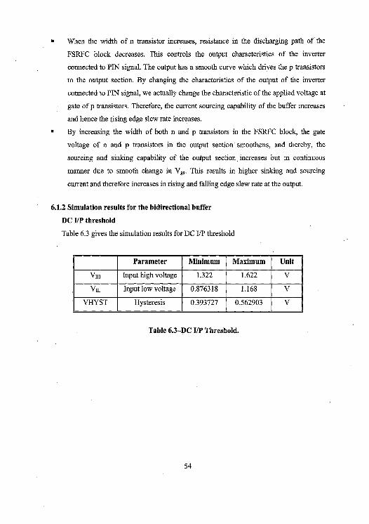
DC I/P threshold
Table 6.3 gives the simulation results for DC UP threshold
Parameter Minimum Maximum Unit
VIH Input high voltage 1.322 1.622 V
Vu Input low voltage 0.876318 1.168 V
VHYST Hysteresis 0.393727 0.562903 V
Table 6.3—DC I/P Threshold.
54
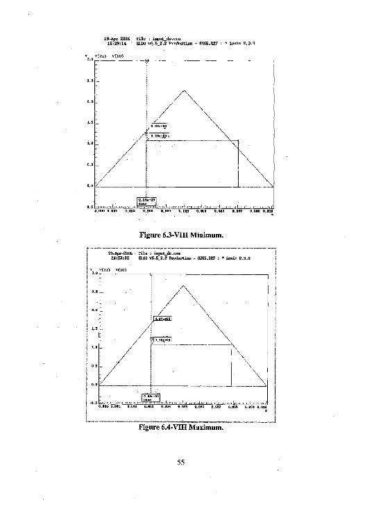
19-Apr-2006 File :-ippptdc.caa 1629:14 ¢D0-v6.5 2.2 P:uducti- - 0265,027 iosim 2.3.8
V(1I) v(10)
Figure 6.3-VIH Minimum.
19-0pc 2006 File : ixryat_dc.cou 16:2302 6502 86.5 2.2. Pcothctiml - 0265027 : ' ipaim 2.3.8
5'{25) V(I0) III
1.69e+00
r
m
0 000~ 001 0 OOi 0 003 9.600 4 000 007 00 9.009 0.010
rigure 6.4-VIH Maximum.
55
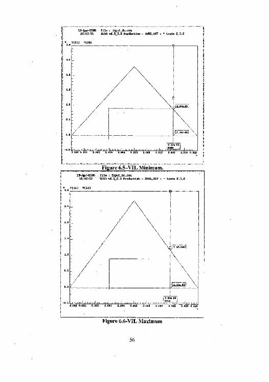
19-Apr-2006- File : iaput_do.ema 16:2855 Hill v6:5_2.2 Peo&oetion - 0265,027: 1ooioo 2.3.8
Y9 v(RI) 5(20)
9.0
1.6 `
1.0
9:6
8 YE 03
0,000 0.031 0.002 0.009" 0.004 0.005 0.006 0.001 0.009 0.909 0:010
Fisure 6.5—VIL Minimum. ]9-Apr-2006 ,:Pile ix11006dc:e0u 16:22:37- -2600 96.5_2.2.Prodoctioo - 0265,027: beam 2.3.8
V x*CZl7 V(ba)
3:5
r~ 1.1]e.oa
o.0
].04e ➢3
1 0.000 0.001 0.002 0.000 0'004 0.005 0,000 0.001 0.000 0.003 0,010
Figure 6.6-VIL Maximum
56
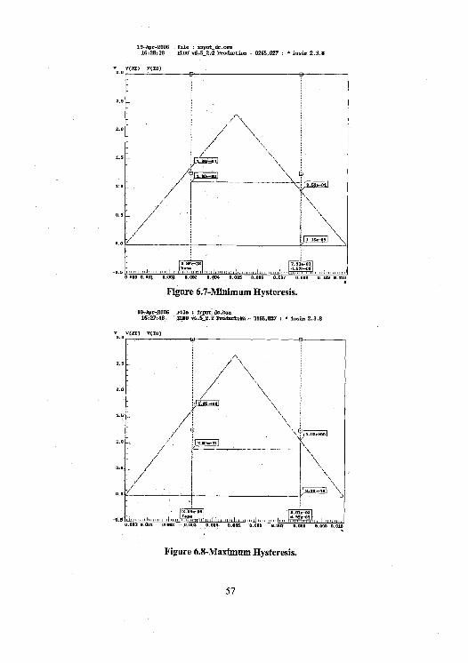
19-Apr-2006 .File io me_dc.ceu 16:28:38 Ella ,6.S_2.2 Production - 0265,027: ' iasim 2.3.8
Y(7i) ' V(10)
0000 0.001 .0.003: 0-003 0.004 0.005 0.006 0.007 0.008 0003 0.0
Figure 6.7-Minimum Hysteresis.
19-4pe-2006' File :: input_dc:tau 16:27:48, ' E100 v6.5 2.2'.Panductiun — 0265,027: • iusim 2.3.0
WOOS 0(605
Figure 6.8-Maximum Hysteresis.
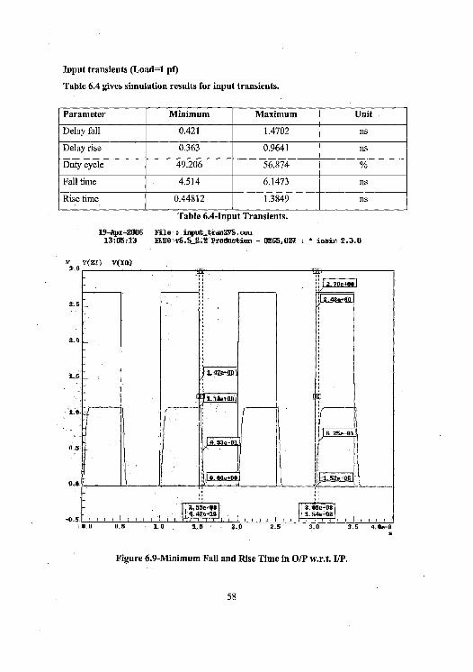
Input transients (Load=1 pf)
Table 6.4 gives simulation results for input transients.
Parameter Minimum Maximum Unit
Delay fall 0.421 1.4702 ns
Delay rise 0.363 0.9641 ns Duty cycle 49.206 56.874 %
Fall time 4.514 6.1473 ns
Rise time 0.44812 1.3849 ns
Table 6.4-Input Transients. 39-Apr-2006 File : ixiput_trmi2V5.cuu 13:05:13 ELUO•v6.5 2.2 Productiam - 0265,027: * iosin 2.3.8
Y - vi5I) v(Ye)
a.70e+00
2.5 1 a.+ISe+00.
2.0
'1.5 _ 1.47e+00.
I. LIe+00
10
f}I~ B_35e-81,I - .4:93e-01 f f
0.5
o,a
1.55e-08 3.05e-08 4.47e-10• 1.54e-08
11 II 0.0 0.5 -.. 1.0- - 1.5 2.0- 2.5 3•.0 3.5 4.Oe-8
Figure 6.9-Minimum Fall and Rise Time in ON w.r.t. I/P.
58
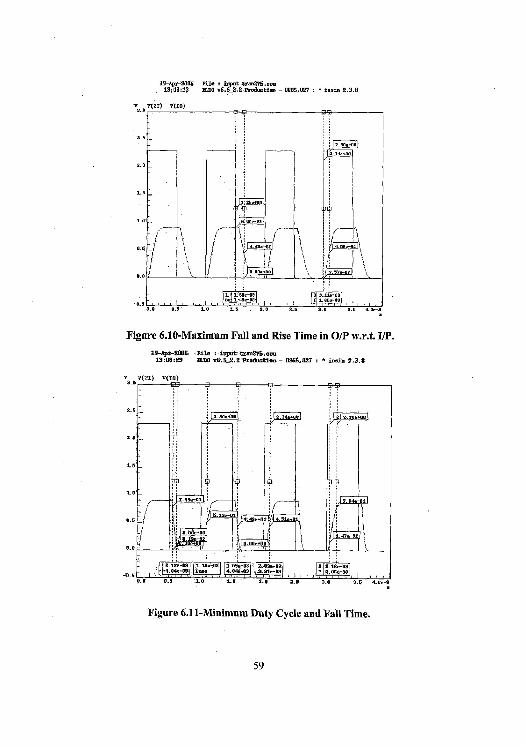
1913
p-2006 File bpt_t0n5u :13
0110 Pod,mti.,, - 0205.027 2.3.0
V V(2I) 1(10>
'p 'p
Figure 6.10-Maximum Fall and Rise Time in 0/P w.r.t. I/P. IS-Apr-2000 File : ioopüt:trso0y5:oo. 1308:29 2150 16.5.2.2 Prothmm-- 0265.027 io.ie 2.3.8
2.5
1.0
1 10
35 ,1..041;0I 88 0.0 0.0 1.0 tO 2.0 tO to 3.5 4.0,-S
Figure 6.11-Minimum Duty Cycle and Fall Time.
59
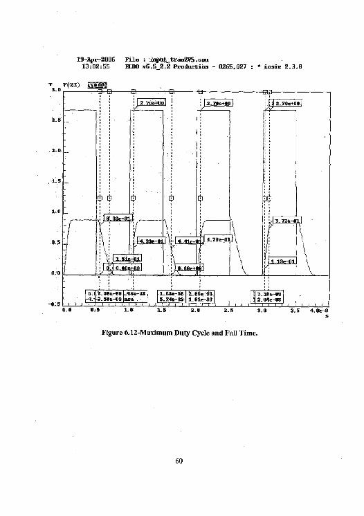
1.0
D:5
0.0
-0.5
19-Apr-2006 File : input_tram2V5.cou 13:02:55 ELDO v6.5_2.2 Production - 0265,027: * iosin 2.3.8
Y3.0 a iTa~y]
8 2Oe+'p0. ;. 2J0e+00 a. TAe+DO.
3E r 0
tDZe-01
1
' '' - .7 73e-011
4,73e-01.S I~ 4.41e.-D. \ Ii 51e
39e-Di
01: 1,:Y9e-D1
0.0. DDe+OU.I 0200e+Di
5 70De-09 D8e-08 1.63e-08 206e-08 3_10e-08 4. 35Se-09 lase . 5.14e-49 1.0]e-08 2.09e-08
1 L .I• I( -I I 3 .I J
1
J( I I I 1
0.0 U.S 1.0 15 - 2.8 2.5 3.0 3.5 4.0e-3 S
Figure 6.12-Maximum Duty Cycle and Fall Time.
60
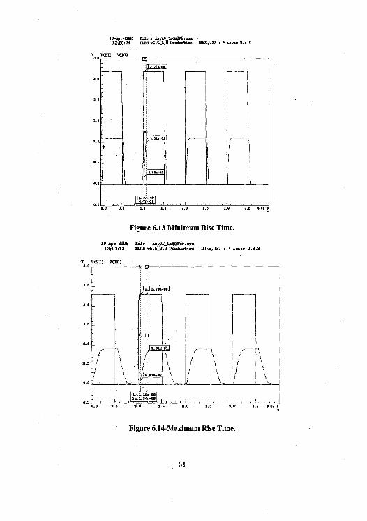
19-Apr-2006. File-: ieput_tre02V6.cw 130824 - fl.00 8.S_22 Froth.cti® -X0265,087 ; iosan. 2.3.8
Figure 6.13-Minimum Rise Time.
19-Apr-2006 File : i*epOtFmi2V5.coee 1304:13 HAD -0052.2 Prod—tim. - 0265.027 iosim 2.3.8
5(23) V(I0)
2.5 41a 20 00
01
a:0
1.6
::L . LL"
}
t t~
8 L343ge-0a
0.5 0.0 0.5 - 10 2.5 2.0 2.5 3.0 3.5 q,Oe-B
Figure 6.14= Maximum Rise Time.
61
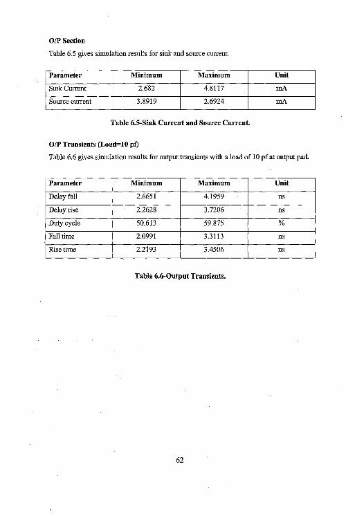
O/P Section
Table 6.5 gives simulation results for sink and source current.
Parameter Minimum Maximum Unit
Sink Current 2.682 4.8117 mA
Source current 3.8919 2.6924 mA
Table 6.5-Sink Current and Source Current.
O/P Transients (Load=10 p1)
Table 6.6 gives simulation results for output transients with a load of 10 pf at output pad.
Parameter Minimum Maximum Unit
Delay fall 2.6651 4.1959 ns
Delay rise 2.2628 3.7206 ns
Duty cycle 50.613 59.875
Fall time 2.0991 3.3113 ns
Rise time 2.2193 3.4506 ns
Table 6.6-Output Transients.
62
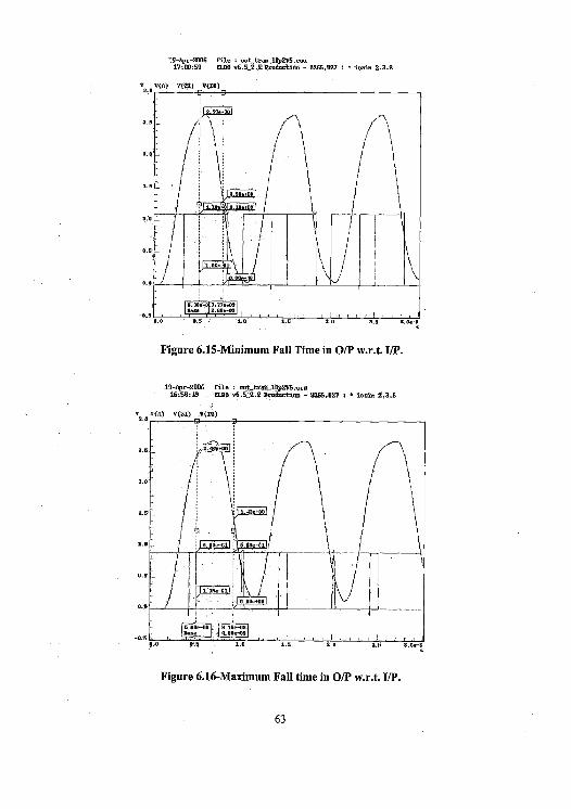
19-Ape-2006 File :•vettree_10p292.emo 1700:50 ELUO -v6.5. 2.2'.Pxoductiml - 0265.027 i iosdw 2.3.8
Figure 6.15-Minimum Fall Time in O/P w.r.t. I/P.
19-npr-2006'. File : out_trar_.10p2V5;coo 16x50:49 ' MMG v6.5_2;2':Prrodooetime - 0265,027: iosee 2.3.8
Figure 6.16-Maximum Fall time in O/P w.r.t. I/P.
63
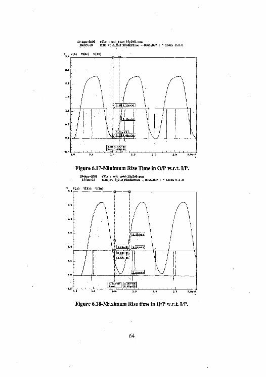
19-Apc-2006' Fi1e :. wt_trar_1O12V5.cw
1659:48. 8120 v6.5.2.2 Prod-time —.0265,027: iosin 2.3.8
V(A) V(2I) V(IO) 9.0
Q.0 ..
Figure 6.17-Minimum Rise Time in O/P w.r.t. I/P. 19-Apr-2006 f49 : aut trot op2V5,cou
17:00:54 SLID 6.52.2.Fro tan - 0265,027: iosim 2.3.0
V(A0 V(2I1 V(Ie1
Figure 6.18-Maximum Rise time in ON w.r.t. I/P.
64
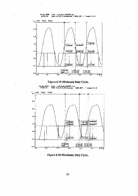
19-Apr-2886 File : aut~teoe_18p2VS.cuu
1659:34 II.UF v6. 2.2 Pooduet ee - 8265,827 : balm 2.3.8
_ V(A) r(2x) V(10)
a. s
a.6
1.0 000
0.H
E~09e. o 0 .00 a. aye-09
➢9. 101e 08.
0.0 -U.s to 1.5. a.0 E.5 3.oe-8
Figure 6.19-Minimum Duty Cycle. 19-Apr-20U6 File : aut-t IIUp2V5.cw
16:58:39 B.DO v6.S 22. PCO&ction -.8265.027 • basin 2.3.8
_P(A) V(81) Y(I8)
Figure 6.20-Maximum Duty Cycle.
65
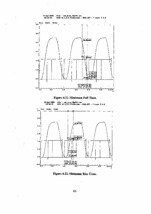
VV(A) V(ZI) V(10) a.b
2.5
a.0
>.s
0.6
0.0
-0.5
19-Apr-2006 File : out_ttmtlUp2V5.eau 16:58:27 IIE0 o6.5_2.2. ,-d=ti- - 0265,027 ° issim 2.3.8
Figure 6.21-Minimum Fall Time. ]9-4.pr-2006 File : uut tron 100205.csu 1658:33 01.50 vG.5 2.2!Prodwtimi - 0265,027: iooiu 2.3.8
V(A) V(ffi) 0(10)
1.5
M
Figure 6.22-Minimum Rise Time.
66
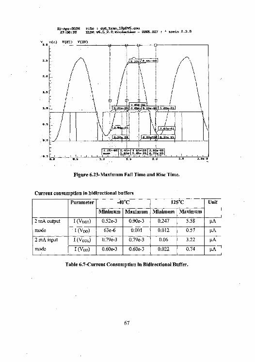
19-Apr 2006 Tile : out tran_10p2VS.cou
17:0038 t.DO ..6.5_2.2 Prgdection - 0265.027 • iosim 2.3.0
It V(A vr7rl v7Tn)
239-0
a.o
1.5
_ 9.0 1.0 ~~ 9.0 a-0 9_ 0' 3. Doe-0i. 9.00e-01.
:1 1 ao~ -0~. y.0ae-01
1]De-O~ 'O. OOe+06 1'. 10e-05
1. ]5e-OB 1.98e1. 69e-OB a.9ae99
-0.5 88se 3.1B(547 8.72e09
7 - - { i 0.0 -- A5 1_0 ---- 1.5 - -- 2.0 2.5 3.0e-8
Figure 6.23-Maximum Fall Time and Rise Time.
Current consumption in bidirectional buffers
Parameter -40°C 125°C Unit
Minimum Maximum Minimum Maximum
2 mA output I (VDDE) 0.52e-3 0.90e-3 0.247 5.58 µA
mode I (VDD) 63e-6 0.001 0.012 0.57 µA
2 mA input I (VDDa) 0.79e-3 0.79e-3 0.06 3.22 µA
mode I (VDD) 0.60e-3 0.60e-3 0.022 0.74 pA
Table 6.7-Current Consumption in Bidirectional Buffer.
67
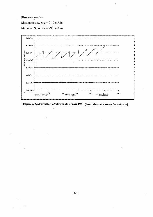
Slew rate results
Maximum slew rate = 21.0 mA/ns
Minimum Slew rate = 29.6 mAJns
Figure 6.24-Variation of Slew Rate across PVT (from slowest case to fastest case).
68

CHAPTER 7
LAYOUT STRATEGY
7.1 Hierarchy
The use of hierarchy involves dividing a module into sub modules and then repeating this
operation on the sub modules until the complexity of the sub modules is at an appropriate
level of detail. This is similar to software application program where large program split into
smaller and smaller sections until simple subroutines, with well defined functions and inter-
faces can be written. Although we can have module at single level but the picture of the
module will not be clear and easily perceivable. In case of hierarchical approach, if some
error occurs in the functionality, then it is easier to focus on the problem and can be
corrected with ease.
7.1.1 Instantiation and hierarchy
Many times in a circuit, certain leaf cell is used many times in the same cell, and that cell
may exist in some library. There are three ways in which that leaf cell can be placed in the
cell, i.e.
• Either by designing the leaf cell from scratch
• By copying the cell from the library and the placing it at the required place
• By just instantiating the leaf cell in the cell. The last method has one major
advantage over the first two, as it reduces redundancy.
By instantiating a cell or leaf cell inside a circuit we just refer that the action to be
performed on the signal at that instance has to be preformed by the cell or leaf cell present in
some library. It helps in DRC and LVS as the cell or leaf cell is already DRC and LVS
clean. So when we run the DRC or LVS we perform these tasks in hierarchal mode.
Hierarchy is nothing but the action performed on the circuit is from top to bottom fashion.
By top to bottom fashion we mean that the task is first performed on the top level, i.e. if
some cells are instantiated in the circuit the direction of flow of action is directed to the
instantiated cell and if again some cells are instantiated in the instantiated cell in the main
69

circuit, then it goes to the cell instantiated in the instantiated cell. Again if we want to go to
the bottom most instantiated cell we can descend into the cell only in hierarchal way.
7.1.2 Calibre
Calibre is the Mentor Graphics batch layout verification toolset, which works on GDSII and
CIF (CalTech Intermediate Format) data, as well as data generated from IC station. Layout
verification is required to check the validity of the layout in context of process and actual
gate level design prior to their testing on silicon. The layout verification is divided into the
following four tasks:
Design Rule Check (DRC) verifies that the physical design rules have been met for every
object in the design. These rules are technology dependent and they require updating as the
technology changes.
Layout Versus Schematic (LVS) verifies that the layout matches the schematic or netlist.
Parasitic Extraction (PEX) presents layout information about parasitic resistance and
parasitic capacitance and back annotating them to corresponding objects in the schematic,
for more accurate simulation. With this information, you can see where to change the layout
to improve chip performance.
Electrical Rule Check (ERC) performs connectivity related checks.
GDS Format
For Calibre DRC and Calibre LVS verification; it is required to generate a netlist of the
layout in GDS format. This format converts the geometrical information of the gate level
logic into a netlist file which sets different codes for different layers used in the layout,
along with its geometrical shape, in the layout, in the form of coordinates. During Calibre
DRC, it basically picks the layer codes and the coordinates for different layers and compares
it with its design rule file drc.ctrl file. This dre.ctrl file contains the defined set of rules for
70

layers spacing and their minimum geometrical shape. Calibre DRC is a fast, high capacity,
and complete design rule check system.
CDL Format
This is a format in which the information about the connectivity of different devices, pins,
and components in a circuit is stored. This netlist is slightly different from spice netlist so
during LVS verification, the tool picks the information about the connectivity of different
layers and their pin configuration and compares it with the schematic netlist which is in
CDL format which actually has the connectivity information about the circuit form
schematic.
7.2 Hierarchy in Layout
In a layout of an I/O, there are two types of cells:
Base cell consists of active, poly-, and transistor. Usually for one library, all the I/Os have
same base cell irrespective of whether its an input, output, or bidirectional with few
exceptions where some modification at the base level is necessary to achieve some
important characteristic which is otherwise not possible in the chip. Base cell has defined
boundaries within itself for different blocks which are needed to design a buffer. In these
defined space, transistors with active and poly for that particular block is present in floating
state, i.e. they are not connected together or some other leaf cell is instantiated.
Leaf Cell can be of two types
• One having only the information about the connectivity of transistors with their pin
information at top level or at the instantiated cell level. They have different metal rails,
vias and pins in their cell view.
• The other type contains active and poly forming the transistor along with some metal
rails used in the cell which is same for all the cells in the library. These cells are
actually instantiated at the base level and can be instantiated inside other leaf cell or
they can instantiate some other leaf cells inside them. They are generally lower in
hierarchy to base cell.
71
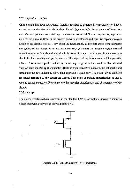
7.2.1 Layout Extraction
Once a layout has been constructed, then it is required to generate its extracted view. Layout
extractors examine the interrelationship of mask layers to infer the existence of transistors
and other components. As metal layers are used to connect different components, to provide
path for the signal to flow, in the process parasitic resistances and parasitic capacitances are
added to the original circuit. They affect the functionality of the chip apart from degrading
the quality of the signal. So an extractor basically calculates the parasitic resistances and
capacitances at each node and adds this information in the extracted view. It is necessary to
check the functionality and performance of the signal taking into account all the parasitic
effects. This is accomplished either by simulating the generated netlist from the extracted
view or back annotating the parasitic effects at their respective nodes in the schematic and
simulating the new schematic view. First approach is quite easy. The output given indicates
the actual response of the circuit on silicon. This helps in making modification in layout
view to reduce parasitic effects to restore the specified functionality and characteristic of the
circuit.
7.3 Latch up
The device structures that are present in the standard CMOS technology inherently comprise
a pnpn sandwich of layers as shown in figure 7.1.
Figure 7.1 (a)-NMOS and PMOS Transistors.
72

II I n I n s n p p
0~ V V n RI
V
(beta(n) + 1)'In beta(n) * In R2 I well 1 t 1p
R1 Øsub
a
I — In "_beta(p) ` Ip e a(p) + 1) ' Ip
Figure 7.1 (b)—Effect of Latchup.
The sandwich can be thought of as a connection between a parasitic pnp and a parasitic
npn transistor. The source of the n-channel transistor forms the emitter of a parasitic
lateral npn transistor, the p-substrate forms the base and the n-well forms the collector.
Also the source of the p-channel transistor forms the emitter of a parasitic pup transistor,
n-substrate as the base and the p-substrate as the collector. Thus, the resulting circuit is
formed.
In the normal mode of operation both the junctions are reversed biased. Problem occurs
when due to some reason one of the two transistors go into the active region. Then a
positive feedback is formed and large currents flows causing breakdown in the CMOS.
This phenomenon is called Latchup.
73

The transistor can go into the active region for a variety of reasons like
■ Application of voltage which is greater than power supply voltage to I/P or O/P
terminal.
• Improper sequencing of power supplies.
• Presence of large DC currents in substrates.
• Flows of displacement currents in the substrate due to fast changing internal
nodes.
Latchup chances increase when the substrate or well concentration is made lighter, as the
well is made thinner and as the device geometries are made thinner. This is because it
increases the resistances and increases the beta of transistors.
Latchup can be prevented by include special protection structure at I/P and O/P pads so
that the excessive currents flowing can be effectively shunted and inclusion of low
impedance diffused "guard rings" surrounding the wells. The latter are formed by using
the source/drain diffusion and provide a low-resistance, equipotent ring in the substrate
and well to lower series resistance.
7.3.1 Tentative latch up design rules
In the figure 7.2(a) shown the green color shown is OD. (active region). In this particular
case OD is working as a guard ring. This active area has got a lot of resistance which aids
in latch up problem. So to minimize the resistance of the OD metall (blue) is placed over
it having as many contacts as can be possible. The metall will come in parallel with OD
and hence minimizing the resistance.
In figure 7.2(b) one of the method called strapping has been done in order to avoid
Latchup problem. In this case the n substrate or p substrate are tied to VDD or ground
respectively as either the case may be for PMOS and NMOS. The figure below shows the
strapping with VDD, i.e. n substrate with the help of vias and different metal layers.
74
Maximal voltage difference: The voltage difference should be calculated in all
application modes of the IP. The highest voltage difference is then used for well
distance rules. Figure 7.3 shows the layout of the bidirectional 110 buffer.
Figure 7.2 (a)-Measure to avoid Latchup.
75
- -- __--__.-- -- -- -
t
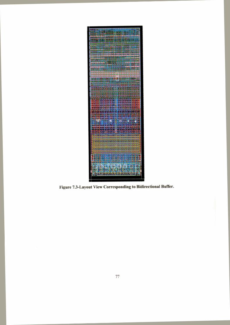
Figure 7.3-Layout View Corresponding to Bidirectional Buffer.
77
CHAPTER 8
CONCLUSION
A comprehensive account of the I/O buffer elements has been presented in this work. The
emphasis is on the circuit design of the several I/O cells and a basic understanding of the
purpose and functionality of the buffer elements. Circuit and design issues relating to
hysteresis and Slew rate control has also been presented. In the present work, slew rate
control has been studied and discussed in more detail. Various design issues related to
hysteresis, level shifting, driving capability, and ESD protections has been discussed too.
The results obtained are good and within the specifications.
An I/O design today is much more than the circuit designs. The circuit limitations can be
well addressed by an efficient layout of the I/O cell. Moreover, it is in the intelligent
layout that 1/0 Latchup (high current through UO make them doubly susceptible to Latch
up) can be prevented. Similarly ESD protection through circuits and technological
modifications has also assumed importance in an UO design. These issues form a separate
topic in themselves and hence have been left out of the present work.
Present work shows that the adjusting the width of transistor of predriver stage can
control the current slew rate. This transistor in the predriver has been replaced by a series
of parallel transistor which are made ON or OFF according to PVT conditions so that to
have an equivalent width of the transistor which results in a slew within the desired
range. Al the worst case, that is, at the slowest PVT corner, all the transistors are turned
ON and at the best case, that is, at the fastest PVT comer, all the transistors are turned
OFF: As we move from slowest to fastest comer, the parallel transistors are made OFF
one be one, so that the equivalent width is goes on reducing as we move towards the fast
comers, which in turn controls the slew from raising above a particular desired value
across all the corners. In case of an I/O buffer without slew rate control, the slew goes on
increasing as we move from slowest to fastest corners.
78
REFERENCES
[1] Rizvi, M., Fundamentals of I/Os, Central Research and development, ST
Microelectronics, Noida, July 2002.
[2] Haseloff, E., Latch-Up, ESD, and Other Phenomena, Application Report
SLYA014A, May 2000.
[3] Chowdhary, V., Central Research and Development, ST Microelectronics, Noida.
[4] Filanovsky, I. M., and Baltes, H., CMOS Schmitt trigger Design, IEEE-
Transactions on circuits and systems-Fundamental theory and applications, Vol. 41,
January 1994.
[5] ST Microelectronics internal doc.
[6] Neil, H. E., Weste, and Eshraghian, K., Principles of CMOS VLSI Design, A systems Perspective, 2nd Edition, Prentice Hall.
[7] Brunty, C., and Gal, L., Optimum tapered Buffer, IEEE-Journal of Solid
State Circuits (JSSC), Vol. 27, No.1, January 1992, pp. 118-119.
[8]. Kwang-Hoon Oh, Investigation of ESD performance in advanced CMOS Technology, A dissertation submitted to the Department of Electrical Engineering and the
committee on graduate studies of Stanford University in partial fulfillment of the
requirements for the award of doctor of philosophy, October 2002.
[9] Razavi, B., Design of analog CMOS integrated circuits. [10] Darbal, S., and Malonery, T. J., Basic ESD and I/O design, Wiley Inter Science
Publication.
79
APPENDIXI
SCHEMATICS
2V5 Bidirectional Buffer
80
VVID ¶Vfà2v5 3ck
'LSjFTR. .r1
t CN
GNDE
Predriver
81
Slew Rate Control Block I (SCB1)
82
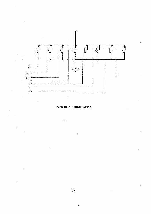
b3 bit
Slew Rate Control Block 2
83
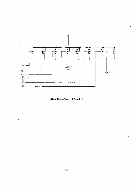
e
63 b2 II
Slew Rate Control Block 2
83
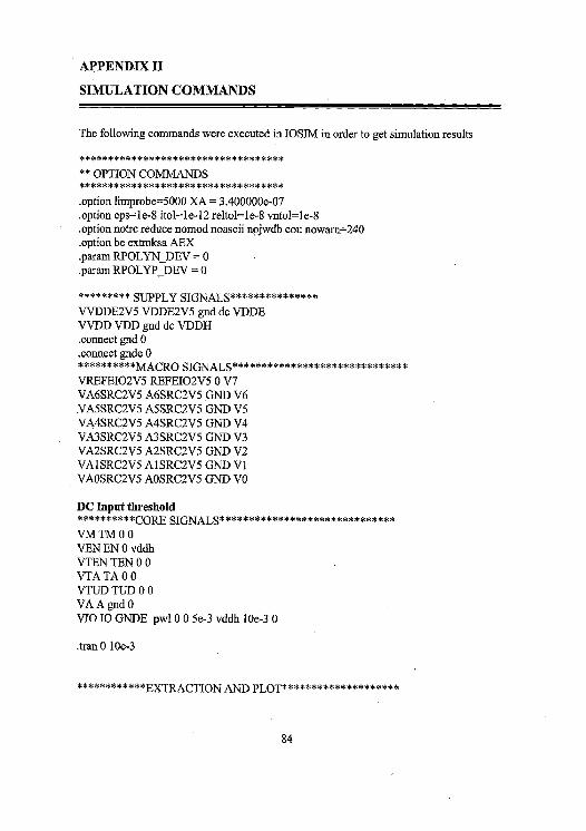
APPENDIX II
SIMULATION COMMANDS
The following commands were executed in IOSIM in order to get simulation results
*********************************** ** OPTION COMMANDS *********************************** .option limprobe=5000 XA = 3.400000e-07 .option eps=le-8 itol=le-12 reltol=le-8 vntol=le-8 .option notrc reduce nomod noascii nojwdb cou nowarn=240 .option be extmksa AEX .param RPOLYN_DEV = 0 .param RPOLYP_DEV = 0
********* SUPPLY SIGNALS*************** VVDDE2V5 VDDE2V5 gnd dc VDDE VVDD VDD gnd dc VDDH .connect gnd 0 .connect grade 0 **********MACRO SIGNALS****************************** VREFEIO2V5 REFEIO2V5 0 V7 VA6SRC2V5 A6SRC2V5 GND V6 VA5SRC2V5 A5SRC2V5 GND V5 VA4SRC2V5 A4SRC2V5 GND V4 VA3SRC2V5 A3SRC2V5 GND V3 VA2SRC2V5 A2SRC2V5 GND V2 VAISRC2V5 AISRC2V5 GND Vi VAOSRC2V5 AOSRC2V5 GND VU
DC Input threshold **********CORE SIGNALS****************************** VMTM00 VEN EN 0 vddh VTENTEN00 VTATA00 VTUD TUD 00 VA A gnd 0 VIO IO GNDE pwl 0 0 5e-3 vddh 10e-3 0
.tran 0 1 Oe-3
************EXTRACTION AND PLOT********************
84
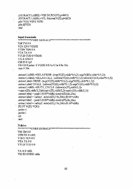
.EXTRACT LABEL=VIH XUP(V(ZI),pvdd/2)
.EXTRACT LABEL=VIL Xdown(V(ZI),pvdd/2)
.plot V(A) V(IO) V(ZI)
.plot I(VIO)
.end
Input transients **********CORE SIGNALS****************************** VMTM00 VEN EN 0 VDDH VTEN TEN 00 VTATA00 VTUD TUD 0 VDDH VAAGND0 CZI ZI 0 1pf VIO TOO pulse 0 VDDE 0 0.1n 0.1n 4.9n lOn .tran 0 20n
.extract LABEL=DELAYRISE (xup(V(ZI),vddh*0.5,2)-xup(V(IO),vdde*0.5,2))
.extract LABEL=DELAYFALL (xdown(V(ZI),vddh*0.5,2)-xdown(V(IO),vdde*0.5,2
.extract label=TRISE (xup(V(ZI),vddh*0.9,2)-xup(V(ZI),vddh*0.1,2))
.extract label=TFALL (xdown(V(ZI),vddh*0.1,2)-xup(V(ZI),vddh*0.9,2))
.extract LABEL=DUTY_CYCLE (xdown(v(ZI),vddh/2,2)- +xup(v(ZI),vddh/2,2))I(xup(v(ZI),vddh/2,2)-xup(v(ZI),vddb/2,3)) .extract label = peakl (0.95*vddh)-max(v(ZI),On,20n) .extract label = valleyl min(v(ZI),15n,20n)-(0.05*vddh) .extract label = peak2 (0.90*vddh)-max(v(ZI),0n,20n) .extract label = valley2 min(v(ZI),l5n,20n)-(0.10*vddh) .PLOT V(ZI) V(IO) .probe v .probe i .op .end
N drive **********CORE SIGNALS****************************** VMTM00 VEN EN 0 vddh VTEN TEN 00 VTATA00 VTUD TUD 00
VA A 0 vddh VIO IO GNDE vdde
85
.tran 0 lu ************EXTRACTION AND PLOT********************
.EXTRACT label = IPDN -(i(VIO))
.EXTRACT label = RPDN abs(V(VDDE2V5)/I(VIO))
.plot I(VIO)
.end
P Drive **********CORE SIGNALS****************************** VMTM00 VEN EN 0 vddh VTEN TEN 00 VTATA00 VTUD TUD 00
VA A 0 vddh VIO IO GNDE vdde
.tran 0 lu ************EXTRACTION AND PLOT********************
.EXTRACT label = IPDN -(i(VIO))
.EXTRACT label = RPDN abs(V(VDDE2V5)/I(VIO))
.plot I(VIO)
.end
Pull down **********CORE SIGNALS****************************** VMTM00 VEN EN 0 vddh VTEN TEN 00 VTATA00 VTUD TUD 00
VA A 0 vddh VIO IO GNDE vdde
.tran 0 lu ************EXTRACTION AND PLOT********************
.EXTRACT label = IPDN -(i(VIO))
.EXTRACT label = RPDN abs(V(VDDE2V5)/I(VIO))
.plot I(VIO)
.end
86
0/P Transients **********CORE SIGNALS****************************** VTMTM00 VENEN00 VTUDTUD00 CIOI00 lop VAAOpulse OVDDHOO.ln0.1n4.9nIon .tran 0 30n
.extract LABEL=DELAYRISE (xup(V(I0),VDDE*0.5,2)-xup(V(A),VDDH*0.5,2))
.extract LABEL=DELAYFALL (xdown(V(I0),VDDE*0.5,2)- +xdown(V(A),VDDH*0.5,2)) .extract LABEL=TRISE (xup(V(I0),VDDE*0.9,2)-xup(V(IO),VDDE*0.1,2)) .extract LABEL=TFALL (xdown(V(IO),VDDE*0.1,2)-xdown(V(I0),VDDE*0.9,2)) .extract LABEL=DUTY_CYCLE (xdown(v(10),VDDE/2,2)- +xup(v(IO), VDDE/2,2))/(xup(v(I0), VDDE/2,2)-xup(v(I0), VDDE/2, 3)) .extract label = peakl (0.95*VDDE)-max(v(IO),On,20n) .extract label = valleyl min(v(IO),15n,20n)-(0.05*VDDE) .extract label = peak2 (0.90*VDDE)-max(v(I0),0n,2On) .extract label = valley2 min(v(IO),15n,20n)-(0.10*VDDE)
PLOT V(A) V(ZI) V(I0)
end
87
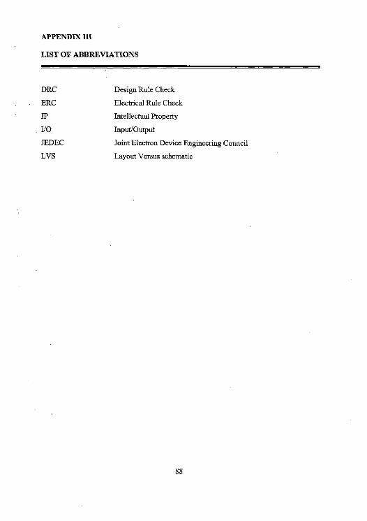
APPENDIX III
LIST OF ABBREVIATIONS
DRC Design Rule Check
ERC Electrical Rule Check
IP Intellectual Property
I/O Input/Output
JEDEC Joint Electron Device Engineering Council
LVS Layout Versus schematic
88