Buffer, Integrator, and Differentiator Op Amps
24
Buffer, Integrator, and Differentiator Op Amps
-
Upload
khangminh22 -
Category
Documents
-
view
4 -
download
0
Transcript of Buffer, Integrator, and Differentiator Op Amps
Buffer, Integrator, and Differentiator Op Amps
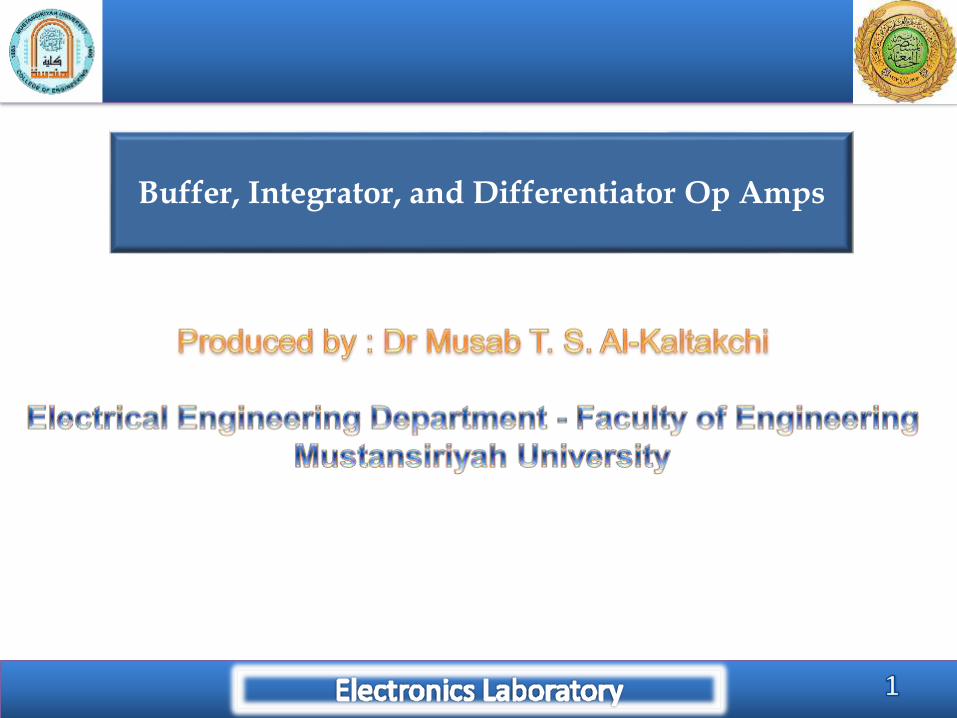
Part1 • Voltage Follower or Buffer
part2• Integrator Op Amp
part3• Differentiator Op Amp
part4
part5
part6
part7
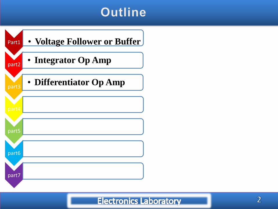
Voltage Follower or BufferWhat is a Voltage Follower?
A voltage follower is also known as a buffer amplifier, unity gain
amplifier, or isolation amplifier
Is an Op-Amp circuit whose output voltage is equal to the input
voltage , so the output voltage follows the input voltage (Vout=Vin)
A voltage follower Op Amp does not amplify the input signal and
has a voltage gain of 1
Gain with feedback or closed loop gain of this circuit is 1
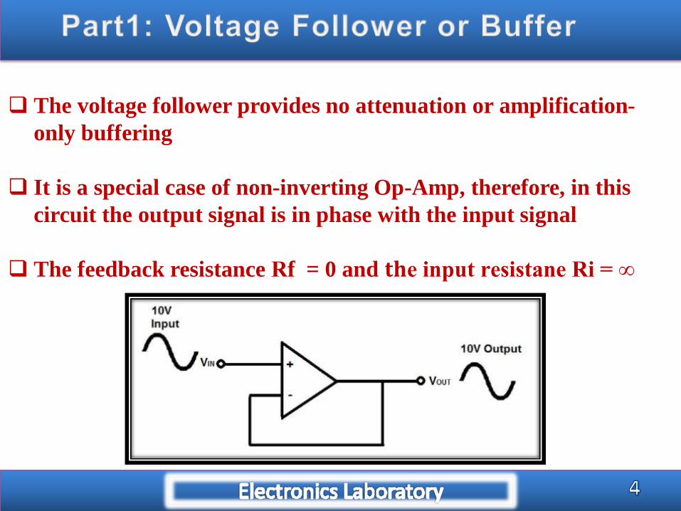
The voltage follower provides no attenuation or amplification-
only buffering
It is a special case of non-inverting Op-Amp, therefore, in this
circuit the output signal is in phase with the input signal
The feedback resistance Rf = 0 and 𝐭𝐡e input resistane Ri = ∞
Advantages of Voltage Followers:
1) Provides power gain and current gain (voltage gain Av = 1)
2) Low output impedance to the circuit, which uses the output of
the voltage follower
3) High input impedance, Op-Amp takes no current from the input
4) Loading effects can be avoided
5) Isolator purpose, to isolate one circuits to another circuit
6) Impedance matching
Applications of Voltage Followers:
1) Buffers for logic circuits
2) Sample and hold circuits
3) Active filters, voltage followers can be used to isolate filter stages
from each other, when building multistage filters
4) Bridge circuit via a transducer

Non-Inverting Circuit Voltage Follower (Buffer) Circuit
Av= vovi= 1+
RfRi
v𝒐 = Av vi
Av= vovi= 1+
0∞
= 1
Rf = 0, Ri = ∞
v𝒐 = vi
-+
-+
The input impedance of the op-amp is very high when a voltage follower or unity gain configuration is used. Sometimes the input impedance is much higher than 1 Megohm. So, due to high input impedance, we can apply weak signals across the input and no current will flow in the input pin from the signal source to amplifier. On the other hand, the output impedance is very low, and it will produce the same signal input, in the output.
Voltage follower circuit is used to create isolation between two different kind of circuits. Due to high input impedance,, so the input current is much lower than the output current while the output voltage follows the input voltage. So the voltage follower provides large power gain across its output. Due to this behavior, Voltage follower used as a buffer circuit and can be used to isolate stages while building multistage filters or some other multistage circuit.
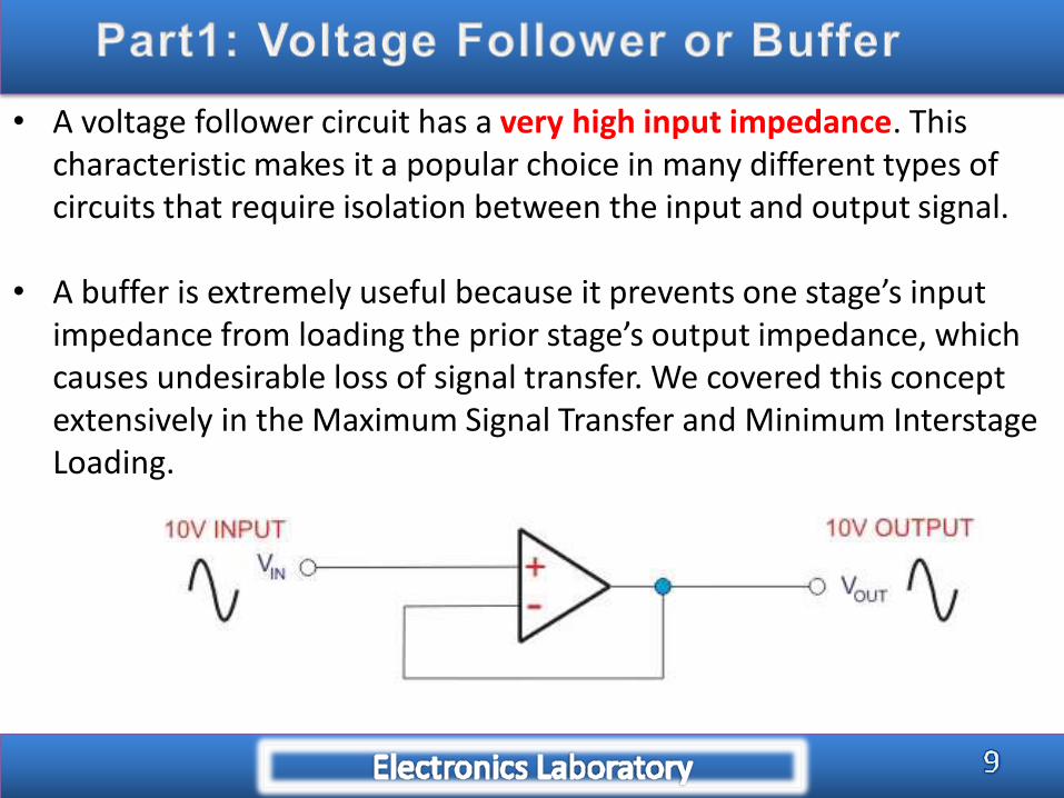
• A voltage follower circuit has a very high input impedance. This characteristic makes it a popular choice in many different types of circuits that require isolation between the input and output signal.
• A buffer is extremely useful because it prevents one stage’s input impedance from loading the prior stage’s output impedance, which causes undesirable loss of signal transfer. We covered this concept extensively in the Maximum Signal Transfer and Minimum InterstageLoading.

• Operational amplifiers have a very high input impedance, which means that they don’t suck in much current (ideally, none) at the inputs. Op amps also have a very low output impedance. One application where this is useful is in a voltage divider. In a voltage divider (as in Figure 2), it’s possible that the impedance load (Ro) can vary quite a bit. Due to Ohm’s Law (V=IR), if Ro varies, it will affect VOUT.
Figure 1: A voltage follower has a gain of one, so (theoretically) the output voltage is equal to the input voltage
Figure 2: A voltage divider, but as Ro varies, VOUT varies due to Ohm’s Law

• In Figure 2, if Ro varies, then VOUT would vary accordingly unless…. you were able to isolate the voltage divider’s VOUT by inserting a high impedance voltage follower between it and Ro, as in Figure 3. Adding a voltage follower to the voltage divider circuit isolates the load impedance (Ro) so that VOUT is dependent upon R1 and R2 (see figure 3), not Ro.
Figure 3: A voltage divider with a voltage follower (unity gain amp) that allows VOUT to remain steady

• The voltage follower (Figure 1) allows us to move from one circuit to another and maintain the voltage level.
• It preserves the voltage source signal.• This is why it’s also called a buffer or isolation amplifier. • You can use a voltage divider circuit to switch from one logic level
(e.g. 5V) to another logic level (e.g., 3.3V). • A cleaner switch is obtained when a voltage follower (buffer
amplifier) is added to the voltage divider circuit (Figure 3). • Another way to accomplish logic level shifting or translation is to
use an IC called a level shifter to accomplish the same buffered transition. The high impedance of the op amp makes it possible for the voltage follower circuit to keep the load (Ro) from affecting the output voltage.
• (Logic levels are used for binary signaling (HI/LOW), not for supplying power, so use a voltage regulator if you need to step down Power (P=VI) to a load. A voltage divider is not a regulator and you could end up smoking a resistor if a voltage divider is used to step-down a power source.)
• With or without a voltage divider circuit, the voltage follower, or voltage buffer, offers a means to transfer a voltage source signal from one impedance level to another without affecting current.
• Ohm’s Law (V=IR) dictates the relationship from there. Voltage followers are used to match impedance in other circuits, too. Note that there is also a current buffer, which preserves the current signal source, rather than voltage signal source.
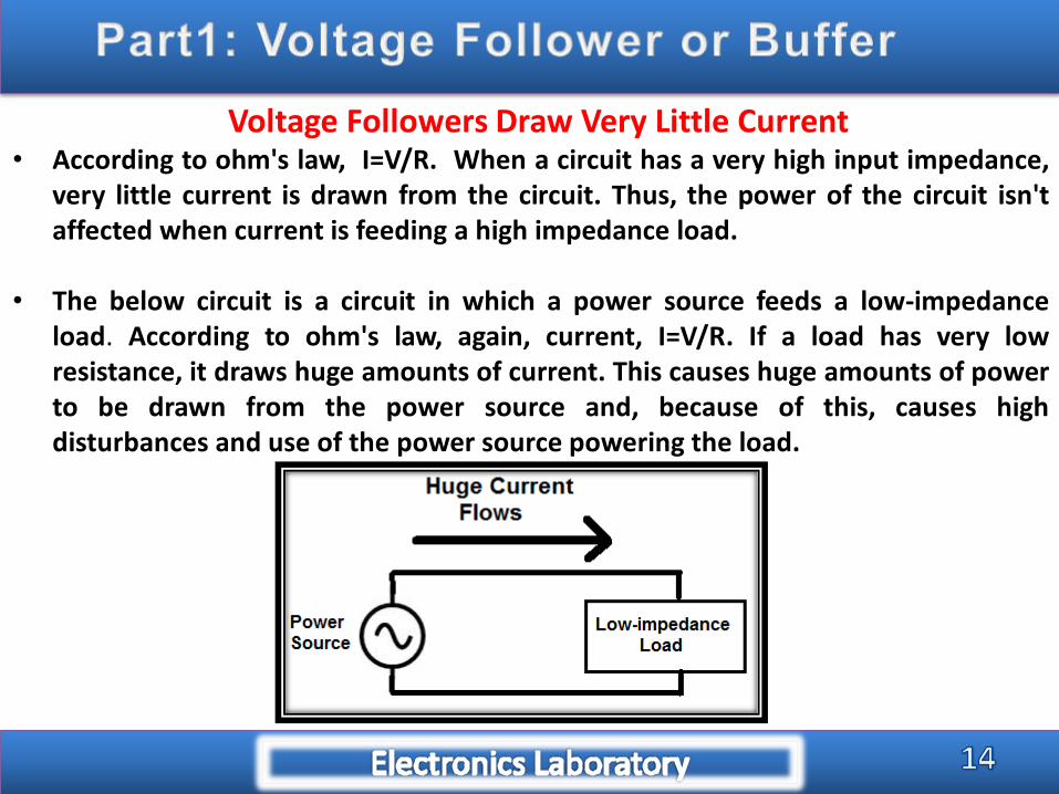
Voltage Followers Draw Very Little Current• According to ohm's law, I=V/R. When a circuit has a very high input impedance,
very little current is drawn from the circuit. Thus, the power of the circuit isn'taffected when current is feeding a high impedance load.
• The below circuit is a circuit in which a power source feeds a low-impedanceload. According to ohm's law, again, current, I=V/R. If a load has very lowresistance, it draws huge amounts of current. This causes huge amounts of powerto be drawn from the power source and, because of this, causes highdisturbances and use of the power source powering the load.

• This circuit below now draws very little current from the power source. Because the op amp has such high impedance, it draws very little current. And because an op amp that has no feedback resistors gives the same output, the circuit outputs the same signal that is fed in.
• This is one of the reasons voltage followers are used. They draw very little current, not disturbing the original circuit, and give the same voltage signal as output. They act as isolation buffers, isolating a circuit so that the power of the circuit is disturbed very little.
Voltage Followers Are Important in Voltage Divider Circuits
One of the reasons voltage followers are used, they simply don't draw a lot of current, so they do not load down the power source.
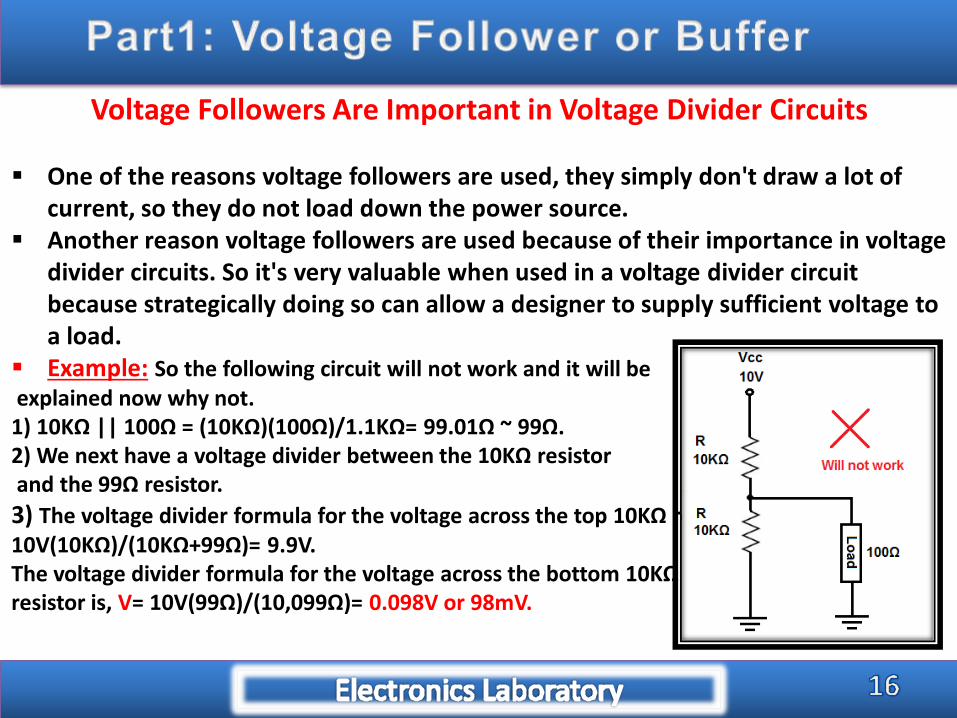
Another reason voltage followers are used because of their importance in voltage divider circuits. So it's very valuable when used in a voltage divider circuit because strategically doing so can allow a designer to supply sufficient voltage to a load.
Example: So the following circuit will not work and it will beexplained now why not.
1) 10KΩ || 100Ω = (10KΩ)(100Ω)/1.1KΩ= 99.01Ω ~ 99Ω.2) We next have a voltage divider between the 10KΩ resistorand the 99Ω resistor.
3) The voltage divider formula for the voltage across the top 10KΩ resistor is, V= 10V(10KΩ)/(10KΩ+99Ω)= 9.9V.The voltage divider formula for the voltage across the bottom 10KΩ resistor and the 100Ω resistor is, V= 10V(99Ω)/(10,099Ω)= 0.098V or 98mV.
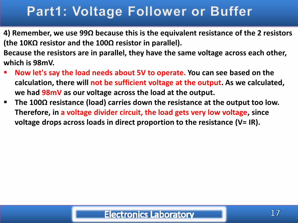
4) Remember, we use 99Ω because this is the equivalent resistance of the 2 resistors (the 10KΩ resistor and the 100Ω resistor in parallel).Because the resistors are in parallel, they have the same voltage across each other, which is 98mV. Now let's say the load needs about 5V to operate. You can see based on the
calculation, there will not be sufficient voltage at the output. As we calculated, we had 98mV as our voltage across the load at the output.
The 100Ω resistance (load) carries down the resistance at the output too low. Therefore, in a voltage divider circuit, the load gets very low voltage, since voltage drops across loads in direct proportion to the resistance (V= IR).
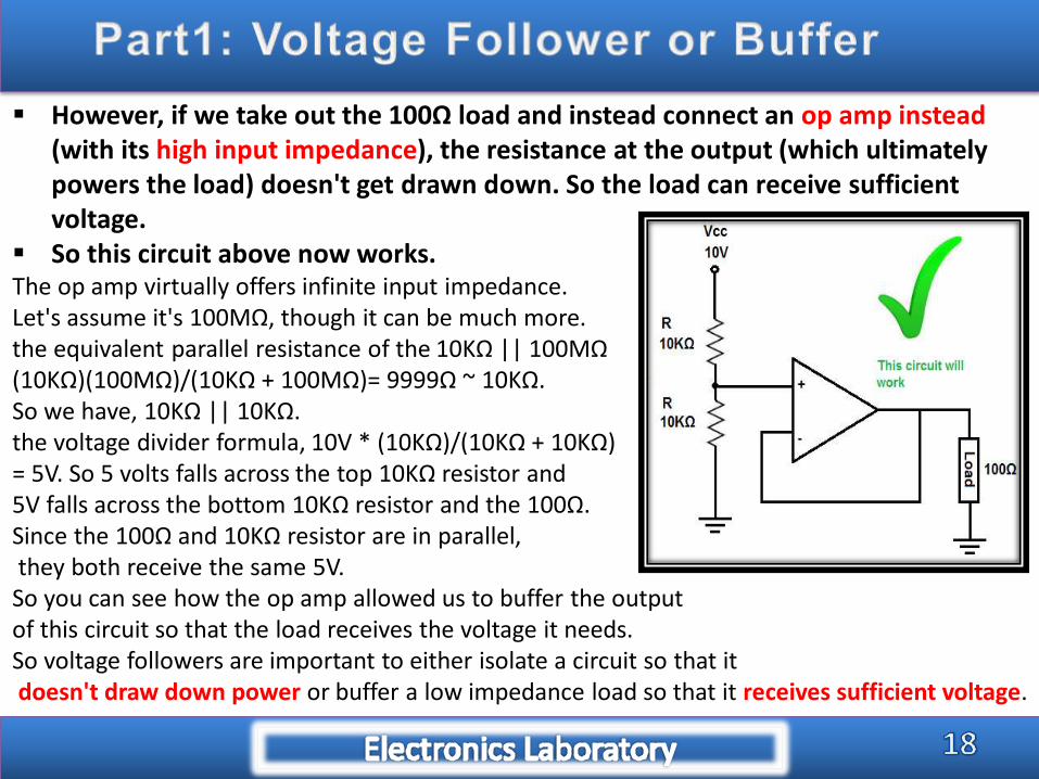
However, if we take out the 100Ω load and instead connect an op amp instead (with its high input impedance), the resistance at the output (which ultimately powers the load) doesn't get drawn down. So the load can receive sufficient voltage.
So this circuit above now works.The op amp virtually offers infinite input impedance. Let's assume it's 100MΩ, though it can be much more.the equivalent parallel resistance of the 10KΩ || 100MΩ (10KΩ)(100MΩ)/(10KΩ + 100MΩ)= 9999Ω ~ 10KΩ.So we have, 10KΩ || 10KΩ.the voltage divider formula, 10V * (10KΩ)/(10KΩ + 10KΩ)= 5V. So 5 volts falls across the top 10KΩ resistor and 5V falls across the bottom 10KΩ resistor and the 100Ω.Since the 100Ω and 10KΩ resistor are in parallel,they both receive the same 5V.
So you can see how the op amp allowed us to buffer the output of this circuit so that the load receives the voltage it needs.So voltage followers are important to either isolate a circuit so that itdoesn't draw down power or buffer a low impedance load so that it receives sufficient voltage.
An integrator is an electronic circuit that produces an output that is the integration of the applied input. This section discusses about the op-amp based integrator.
An op-amp based integrator produces an output, which is an integral of the input voltage applied to its inverting terminal.
It is a circuit designed with Op-Amp in such a way that it performs the mathematical Integration operation
its output is proportional to the amplitude and time duration of the input applied.
The integrator circuit layout is same as a inverting amplifier but the feedback resistor is replaced by a capacitor which make the circuit frequency dependent.

In this case the circuit is derived by the time duration of input applied which results in the charging and discharging of the capacitor.
Initially when the voltage is applied to integrator the uncharged capacitor allows maximum current to pass through it and no current flows through the Op-Amp due to the presence of virtual ground,
the capacitor starts to charge at the rate of RC time constant and its impedance starts to increase with time and a potential difference is develops across the capacitor resulting in charging current to decrease.
This results in the ratio of capacitor's impedance and input resistance increasing causing a linearly increasing ramp output voltage that continues to increase until the capacitor becomes fully charged.
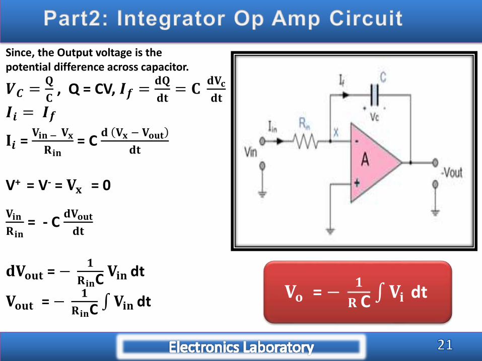
Since, the Output voltage is thepotential difference across capacitor.
𝑽𝑪 =𝐐
𝐂, Q = CV, 𝑰𝒇 =
𝐝𝐐
𝐝𝐭= 𝐂
𝐝𝐕𝐜
𝐝𝐭
𝑰𝒊 = 𝑰𝒇
𝐈𝒊 = 𝐕𝐢𝐧 − 𝐕𝐱
𝐑𝐢𝐧= C
𝐝 𝐕𝐱 − 𝐕𝐨𝐮𝐭
𝐝𝐭
V+ = V- = 𝐕𝐱 = 0
𝐕𝐢𝐧
𝐑𝐢𝐧= - C
𝐝𝐕𝐨𝐮𝐭
𝐝𝐭
𝐝𝐕𝐨𝐮𝐭 = −𝟏
𝐑𝐢𝐧C 𝐕𝐢𝐧 dt
𝐕𝐨𝐮𝐭 = −𝟏
𝐑𝐢𝐧C 𝐕𝐢𝐧 dt𝐕𝐨 = −
𝟏
𝐑 C 𝐕𝐢 dt
A differentiator is an electronic circuit that produces an output equal to the first derivative of its input. This section discusses about the op-amp based differentiator in detail.
An op-amp based differentiator produces an output, which is equal to the differential of input voltage that is applied to its inverting terminal.
In the differentiator circuit the input is connected to the inverting output of the Op-Amp through a capacitor(C) and a negative feedback is provided to the inverting input terminal through a resistor(Rf)
which is same as an integrator circuit with feedback capacitor and input resistor being replaced with each other.
Here the circuit performs a mathematical differentiation operation, and the output is the first derivative of the input signal, 180' out of phase and amplified with a factor Rf*C.
The capacitor on the input allows only the AC component and restrict the DC, at low frequency the reactance of capacitor is very high causing a low gain and high frequency vice versa but and high frequency the circuit becomes unstable.
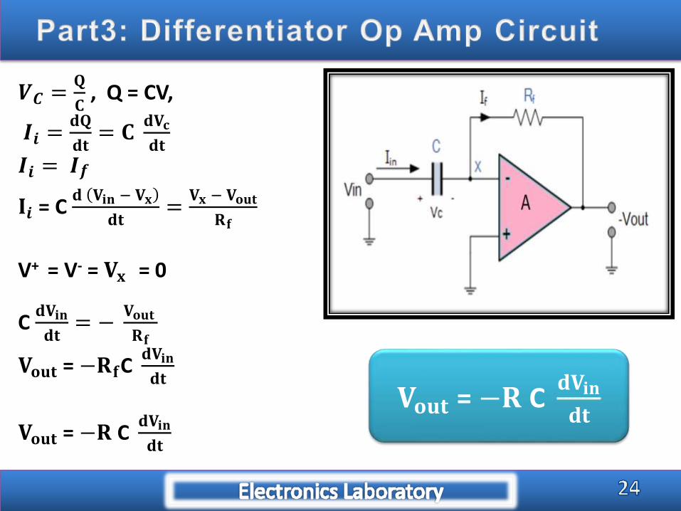
𝑽𝑪 =𝐐
𝐂, Q = CV,
𝑰𝒊 =𝐝𝐐
𝐝𝐭= 𝐂
𝐝𝐕𝐜
𝐝𝐭
𝑰𝒊 = 𝑰𝒇
𝐈𝒊 = C 𝐝 𝐕𝐢𝐧 − 𝐕𝐱
𝐝𝐭=
𝐕𝐱 − 𝐕𝐨𝐮𝐭
𝐑𝐟
V+ = V- = 𝐕𝐱 = 0
C 𝐝𝐕𝐢𝐧
𝐝𝐭= −
𝐕𝐨𝐮𝐭
𝐑𝐟
𝐕𝐨𝐮𝐭 = −𝐑𝐟C𝐝𝐕𝐢𝐧
𝐝𝐭
𝐕𝐨𝐮𝐭 = −𝐑 C𝐝𝐕𝐢𝐧
𝐝𝐭
𝐕𝐨𝐮𝐭 = −𝐑 C𝐝𝐕𝐢𝐧
𝐝𝐭