
FLUID AMPLIFIER DIGITAL INTEGRATOR - NASA Technical ...
91
J c ., -.I w- . , * % NASA CONTRACTOR REPORT h *o M pe: I FLUID AMPLIFIER DIGITAL INTEGRATOR by R. K. Rose Prepared under Contract No. NAS 8-5408 by GENERAL ELECTRIC COMPANY Schenectady, N. Y. for George C. Marshall Space Flight Center NATIONAL AERONAUTICS AND SPACE ADMINISTRATION 0 WASHINGTON, D. C. 0 MARCH 1966
-
Upload
khangminh22 -
Category
Documents
-
view
3 -
download
0
Transcript of FLUID AMPLIFIER DIGITAL INTEGRATOR - NASA Technical ...
J c
. , - . I w- . , * %
N A S A C O N T R A C T O R R E P O R T
h *o M
pe: I
FLUID AMPLIFIER DIGITAL INTEGRATOR
by R. K. Rose
Prepared under Contract No. NAS 8-5408 by GENERAL ELECTRIC COMPANY Schenectady, N. Y. for George C. Marshall Space Flight Center
N A T I O N A L A E R O N A U T I C S A N D S P A C E A D M I N I S T R A T I O N 0 WASHINGTON, D. C. 0 MARCH 1966
FLUID AMPLIFIER DIGITAL INTEGRATOR
By R. K. Rose
Distribution of th i s repor t is provided in the interest of information exchange. Responsibil i ty for the contents r e s ides i n the author or organizat ion that prepared it.
Prepared under Cont rac t No. 8-5408 by GENERAL ELECTRIC COMPANY
Schenectady, N. Y.
fo r George C. Marshal l Space Fl ight Center
NATIONAL AERONAUTICS AND SPACE ADMINISTRATION
For sale by the Clearinghouse for Federal Scientific and Technical information Springfield, Virginia 22151 - Price $3.00
I

ABSTRACT
The digital integrator is a basic building block in digital computation and control systems which can be used to solve non-linear differential equations, multiply, and generate functions. Integration can be performed with respect t o t ime or any other variable.
The f luid amplifier implementation of the applicable digital logic equations is presented. Thir ty-seven OR-NOR, fl ip-flop, and digital amplifier elements were assembled into a c i rcui t compris ing an adder , shif t regis teq and comple- menter . The experimental d igi ta l in tegrator used ser ia l implementat ion of 5 bit words and was opera ted at a nominal 100 cps clock frequency.
Experimental resul ts are presented which show the integrator 's response to a step input as well as a l l of the detailed ari thmetic operations within the integrator . An application showing the interconnection of integrators into a digital-differential-analyzer navigation system is included.
iii

FOREWORD
The f luid amplifier digital-integrator development work descr ibed in th i s repor t w a s car r ied ou t as T a s k 2, P h a s e 111 of a NASA fluid amplifier program Research and Develop- ment - Fluid Amplifiers and Logic" (contract NAS 8-5408). The work was sponsored by the Astrionics Laboratory at the George C. Marshall Space Flight Center, Huntsvil le, Alabama. The digi ta l - integrator development program was joint ly se- lected by Mr. R. E. Currie and Advanced Technology Labora- t o r i e s pe r sonne l a s a key project for future application of fluid amplifiers for digital computation and control systems.
I 1
The development work w a s ca r r i ed ou t at the Advanced Technology Laboratories in Schenectady, New York. This r epor t w a s prepared by Mr . R . K. Rose who was the pr in- cipal development engineer for this work. Other major con- t r i bu to r s t o t he p rog ram were Mess r s . H. W. Avery, E. P. Kexel, E. B. Krulewich and R. E. Otten.

Section
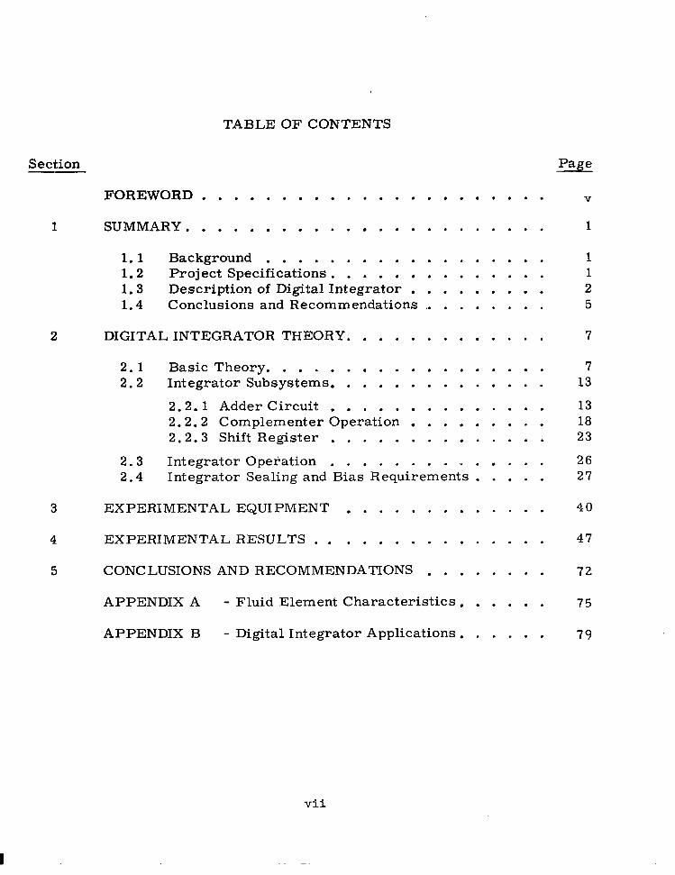
TABLE OF CONTENTS
Page
FOREWORD . . . . . . . . . . . . . . . . . . . . . . V
1 SUMMARY . . . . . . . . . . . . . . . . . . . . . . . 1
1.1 Background . . . . . . . . . . . . . . . . . . 1 1.2 Project Specifications . . . . . . . . . . . . . . 1 1.3 Descript ion of Digital Integrator . . . . . . . . . 2 1.4 Conclusions and Recommendations . . . . . . . . . 5
2 DIGITAL INTEGRATOR THEORY . . . . . . . . . . . . . 7
2.1 Basic Theory . . . . . . . . . . . . . . . . . . 7 2.2 Integrator Subsystems . . . . . . . . . . . . . . 13
2.2.1 Adder Circui t . . . . . . . . . . . . . . 13 2 . 2 . 2 Complementer Operat ion . . . . . . . . . 18 2.2.3 Shift Register . . . . . . . . . . . . . . 23
2.3 Integrator Operat ion . . . . . . . . . . . . . . 2 6 2.4 Integrator Sealing and Bias Requirements . . . . . 2 7
3 EXPERIMENTAL EQUIPMENT . . . . . . . . . . . . . 40
4 EXPERIMENTAL RESULTS . . . . . . . . . . . . . . . 4 7
5 CONCLUSIONS AND RECOMMENDATIONS . . . . . . . . 72
APPENDIX A . Fluid E lement Charac te r i s t ics . . . . . . 75
I
APPENDIX B . Digital Integrator Applications . . . . . . 79
v i i
.
Section 1
SUMMARY
1.1 BACKGROUND
The digital integrator is the basic building block in digital differential
analyzer (DDA) systems just as the operational amplifier serves as the basic
building block in analog computational systems. Appendix B describes typical
applications of digital integrators. The use of digital computation has two
major advantages over analog computation: accuracy and application flexibility.
Practically any desired accuracy can be obtained by increasing the number of
bits in the digital number. Digital computers can handle the multiplication of
independent variables and nonlinear terms much more conveniently and
accurately than analog computers. The major disadvantage of digital compu-
tation is the larger number of functional elements required.
Digital computation circuits may be either serial o r parallel in imple-
mentation, depending on the method of handling the bits which make up a num-
ber. The circuits may be synchronously controlled by a "clock1', o r may be
asynchronously controlled such that each operation triggers the next. The
equipment developed under this program is the synchronously controlled
serial word type.
The u s e of fluid amplifiers with no moving parts for digital computation
systems is of interest primarily because of their environmental tolerance and
their expected long life (shelf and operating). Their tolerance to both nuclear
and electromagnetic radiation and to extreme temperature ranges appears
limited only by the fabrication material. Shock and vibration tolerance also
appear excellent; fluid amplifiers have withstood vibration levels as high as
50 g at 5000 cycles per second. In addition to these advantages it appears
that production costs of fluid amplifier components can be low because of the
lack of close fitting moving parts and bearing surfaces.
1.2 PROJECT SPECIFICATIONS
Since the digital integrator (DI) is the basic building block for digital
computation systems, it w a s chosen as the most appropriate component to
1
study the feasibility of fluid amplifier implementation for such systems. The
development plan selected consisted of two phases; 1) design of the fluid am-
plifier DI, and 2,) fabrication of experimental hardware. The requirements of
the DI were selected to permit use of existing fluid amplifier devices where
possible. The resulting specifications were established as follows:
word capacity 5 -bit
clock rate 100 pulses per second
iteration rate 20 per second fluid amplifier size 0.040'' x 0. 040" power nozzles
operating fluid a i r
supply pressures 5 psig
The selection of the 5-bit word represents a tradeoff between develop-.
ment cost and accomplishment of the project objectives. The 5-bit word is
sufficient to obtain all the feasibility and application information expected from
the project without the extra expense associated with a large amount of hard-
ware complexity. The 5 bits produce a resolution of 1 part in 32; 10 bits
would give resolution of 1 part in 1024.
The clock speed of 100 pulses per second is a reasonable response range
for the available elements which had been selected. Higher speeds would
probably be desired in specific applications but this is basically a problem in
selection of suitable elements rather than a question of fundamental feasibility
of the fluid digital integrator.
One reason for selecting the rather large elements (0. 040" x 0.040")
was their availability. Another reason was the problem of obtaining suitable
test instrumentation for use with smaller elements. Instrumentation is cer-
tain to become a problem in future applications where small size and the need
for monitoring and test instrumentation become critical.
1.3 DESCRIPTION OF DIGITAL INTEGRATOR
The basic computation performed by the digital integrator is integration
of one variable with respect to a second variable, i. e . ,
z = j y d x
2
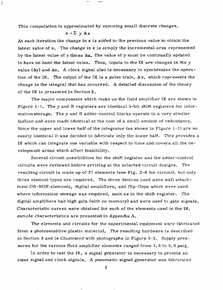
This computation is approximated by summing small discrete changes,
z = c y A x
At each iteration the change in z is added to the previous value to obtain the
latest value of z. The change in z is simply the incremental area represented
by the latest value of y t imes Ax, The value of y must be continually updated
to have on hand the latest value. Thus, inputs to the DI are changes in the y
value (Ay) and Ax. A clock signal also is necessary to synchronize the opera-
tion of the DI. The output of the DI is a pulse train, Az, which represents the
change in the integral that has occurred. A detailed discussion of the theory
of the DI is presented in Section 2 .
The major components which make up the fluid amplifier DI a r e shown in
Figure 1- 1. The y and R reg is te rs are identical 5-bit shift registers for infor-
mation storage. The y and R adder-control blocks operate in a very s imilar
fashion and were made identical at the cost of a small amount of redundancy.
Since the upper and lower half of the integrator (as shown in Figure 1- 1) are s o
nearly identical it w a s decided to fabricate only the lower half. T h i s provides a
DI which can integrate one variable with respect to t ime and covers all the de-
velopment areas which affect feasibility.
Several circuit possibilities for the shift register and the adder-control
circuits were reviewed before arriving at the selected circuit designs. The
resulting circuit is made up of 37 elements (see Fig. 2-8 for circuit) , but only
three element types are required. The three devices used were w a l l attach-
ment OR-NOR elements, digital amplifiers, and flip-flops which w e r e used
where information storage was required, such as in the shift register. The
digital amplifiers had high gain (with no memory) and w e r e used to gate signals.
Characterist ic curves w-ere obtained for each of the elements used in the DI;
sample characterist ics are presented in Appendix A.
The elements and circuits for the experimental equipment were fabricated
from a photosensitive plastic material. The resulting hardware is described
in Section 3 and is i l lustrated with photographs in Figure 3-2 . Supply pres -
sures for the various fluid amplifier elements ranged from 1. 6 to 5. 0 psig.
In order to tes t the DI, a signal generator is necessary to provide an input signal and clock signals. A pneumatic signal generator w a s fabricated
3

-
- - - A y Control * I Y Storage Regis te r - c_ + AY Adder and
\ r
d - yL
t d-
R Storage Regis ter
p + A Z - - + - AX Adder and
(Remainder) Control
F igure 1.1. Simplified Digital Integrator Block Diagram.
4
for testing the equipment and is described in Section 3. This signal generator
provides a 5-bit binary number for the value of y injected into the half DI
(See Figure 1-11; it also generates the 100 pps clock signal, a reset signal
pulse and a read pulse. In a DDA system these clock signals could be supplied
by a fluid amplifier multivibrator. The binary number y, applied by the signal
generator, of course would be generated by the other half of the DI(y)register
and adder. The A y and Ax input pulses would be generated by other DI's in a
computation system. With the pneumatic signal generator it was convenient
to supply a constant value of y, resulting in a simple test to determine the per-
formance of the integrator half. Since the half DI provides integration with
respect to time, a constant value of y results in the time integration of a con-
stant producing a ramp output signal. Results of this and other tests carried
out on the experimental equipment are described in Section 4. Several "open-
loop" tests first were performed to confirm proper operation of the register
and adder-control components. Then the complete system was tested ''closed
loop" to verify operation of the complete circuit. Verification of proper opera-
tion was established by comparing the test results with the results from a
digital computer program which simulated operation of the DI.
1.4 CONCLUSIONS - AND RECOMMENDATIONS ~" -"-___"_I
The results of this program are convincing that digital computation sys-
tems using fluid amplifiers are practical. The response speed of the fluid
systems is adequate for many space applications; the potential for reliability
in adverse environments such as nuclear radiation, heat and vibration is
superior to electronic circuitry. Typical applications which have been con-
sidered are a satellite attitude control, and a guidance computer for an escape 1 1 lifeboat for manned orbital stations.
The work done on this project has dealt only with the digital integrator
since i t was considered a key feasibility problem for digital systems. For
any specific application it will be necessary to consider other parts of the sys-
tem such as power supply, sensors, displays and digital/analog converters.
Investigation of these areas can be pursued most economically by considering
specific application requirements.
As far as the digital integrator itself is concerned, the following repre-
sent areas where additional effort should be applied:
31. miniaturization
j '-2. speed i ~ 3. power consumption
'.4. packaging design and fabrication techniques
5. instrumentation.
The work in these areas is closely interrelated. Miniaturization is required
to improve speed and to reduce power consumption; the degree of miniaturiza-
tion wi l l affect the instrumentation requirements for monitoring and test, and
wi l l dictate certain fabrication methods. The package design must permit very
close coupling of elements to achieve high operating speeds. Theserecom-
mended work areas are discussed further in Section 5.
6
Section 2
DIGITAL INTEGRATOR THEORY
2 . 1 BASIC THEORY
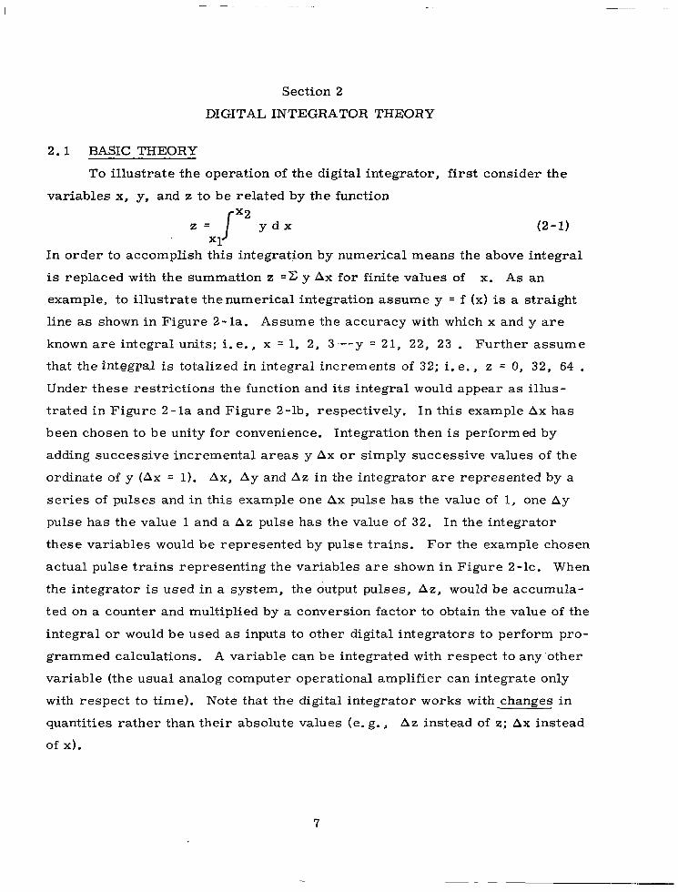
To illustrate the operation of the digital integrator, first consider the
variables x, y, and z to be related by the function
z = IX2 y d x (2-1) X 1
In order to accomplish this integration by numerical means the above integral
is replaced with the summation z =c y Ax for finite values of x. As an
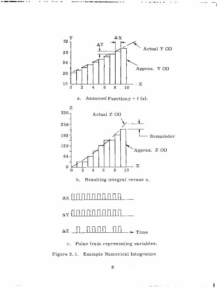
example, to illustrate thenumerical integration assume y = f (x) is a straight
line as shown in Figure 2-la. Assume the accuracy with which x and y a r e
known are integral units; i. e., x = 1, 2, 3 --y = 21, 22, 23 . Further assume
that the i.nt.@gpal is totalized in integral increments of 32; i. e., z = 0, 32, 64 . Under these restrictions the function and its integral would appear as i l lus-
trated in Figure 2 - la and Figure 2-lb , respectively. In this example Ax has
been chosen to be unity for convenience. Integration then is performed by
adding successive incremental areas y Ax or simply successive values of the
ordinate of y (Ax = 1). Ax, Ay and A z in the integrator are represented by a
ser ies of pulses and in this example one Ax pulse has the value of 1, one Ay
pulse has the value 1 and a Az pulse has the value of 32. In the integrator
these variables would be represented by pulse trains. For the example chosen
actual pulse trains representing the variables are shown in Figure 2-lc. When
the integrator is used in a system, the output pulses, Az , would be accumula-
ted on a counter and multiplied by a conversion factor to obtain the value of the
integral or would be used as inputs to other digital integrators to perform pro-
grammed calculations. A variable can be integrated with respect to any other
variable (the usual analog computer operational amplifier can integrate only
with respect to time). Note that the digital integrator works with changes in
quantities rather than their absolute values (e. g., Az instead of z ; Ax instead
of x).
7
32
2 8
2 4
2 0
16
Y A X
Actual Y (X)
prox. Y (X)
0 . 2 4 6 8 10 LL
a. Assumed Funct iony = f (x).
2
Actual 2 (X)
2 5 6 1
192
128
64
0
lT Remainder
r Approx. 2 (X)
-x 10
b. Resul t ing integral versus x.
AZ r T i m e
c. Pulse t ra in represent ing var iab les .
F igu re 2. 1. Example Numerical Integrat ion
8
.. .. .
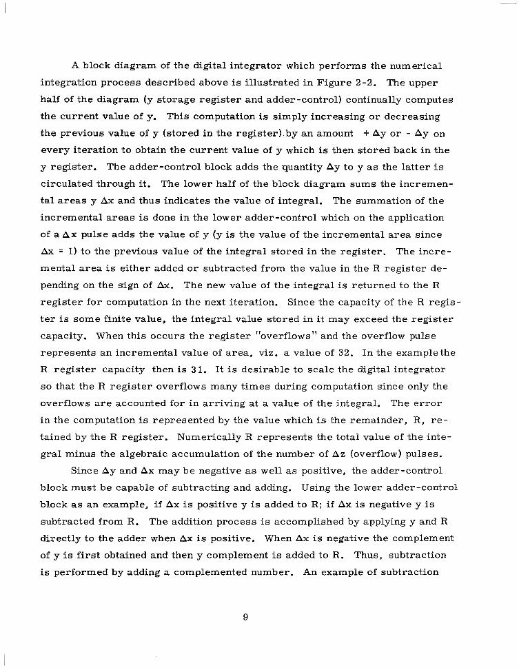
A block diagram of the digital integrator which performs the numerical
integration process described above is illustrated in Figure 2-2. The upper
half of the diagram (y storage register and adder-control) continually computes
the current value of y. This computation is simply increasing or decreasing
the previous value of y (stored in the register).by an amount + Ay or - Ay on
every iteration to obtain the current value of y which is then stored back in the
y register. The adder-control block adds the quantity Ay to y as the latter is
circulated through it. The lower half of the block diagram sums the incremen-
tal areas y Ax and thus indicates the value of integral. The summation of the
incremental areas is done in the lower adder-control which on the application
of a Ax pulse adds the value of y (y is the value of the incremental area since
Ax = 1) to the previous value of the integral stored in the register. The incre-
mental area is either added or subtracted from the value in the R register de-
pending on the sign of Ax. The new value of the integral is returned to the R
register for computation in the next iteration. Since the capacity of the R regis-
t e r is some finite value, the integral value stored in it may exceed the register
capacity. When this occurs the register overflows'' and the overflow pulse
represents an incremental value of area, viz. a value of 32. In the examplethe
R register capacity then is 31. It is desirable to scale the digital integrator
so that the R register overflows many times during computation since only the
overflows a r e accounted for in arriving at a value of the integral . The error
in the computation is represented by the value which is the remainder, R, r e -
tained by the R register. Numerically R represents the total value of the inte-
gral minus the algebraic accumulation of the number of Az (overflow) pulses.
Since Ay and Ax may be negative as wel l as positive, the adder-control
1 1
block must be capable of subtracting and adding. Using the lower adder-control
block as an example, i f Ax is positive y is added to R; i f Ax is negative y is
subtracted from R. The addition process is accomplished by applying y and R
directly to the adder when Ax is positive. When Ax is negative the complement
of y is first obtained and then y complement is added to R. Thus, subtraction
is performed by adding a complemented number. An example of subtraction
9
9-
- Y Storage Regis te r Adder and
Control
lYL - R Storage Regis te r - *
(Remainder) Adder and
Control
+ AY - AY
-k - AX
-t - AZ
Figure 2 . 2 . Simplified Digital Integrator Block Diagram.
10
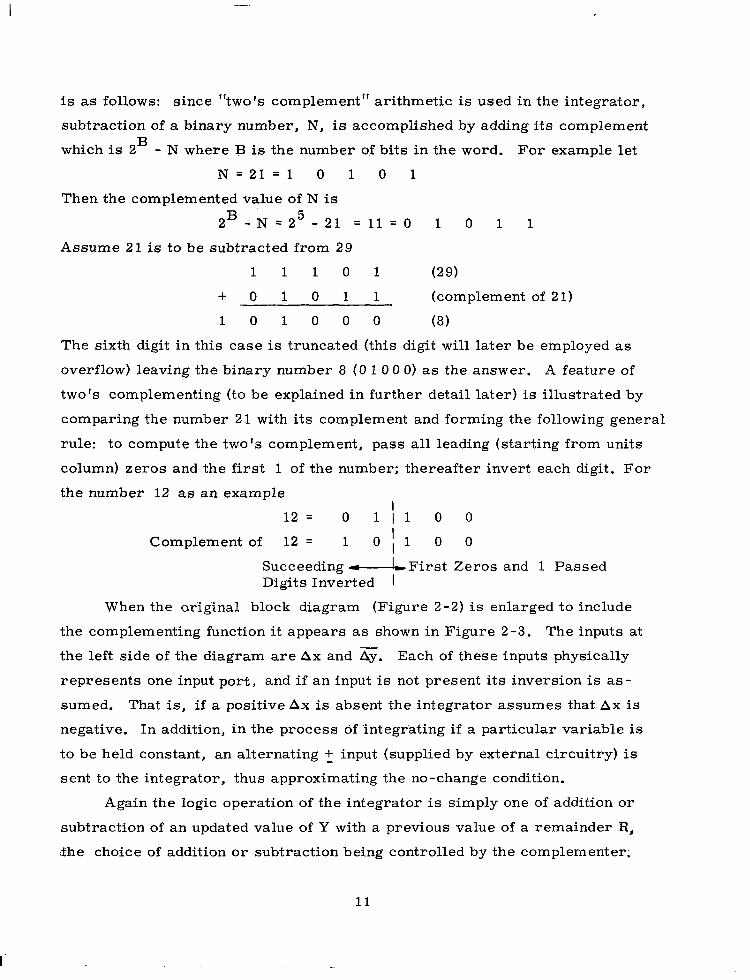
is as follows: since "two's complement" arithmetic is used in the integrator,
subtraction of a binary number, N, is accomplished by adding its complement
which is aB - N where B is the number of bits in the word. For example let
N = 2 1 = 1 0 1 0 1
Then the complemented value of N is
2 B - ~ = 2 5 - 2 1 = H = O 1 o 1 1
Assume 21 is to be subtracted from 29
1 1 1 0 1 (29)
+ 0 1 0 1 1 - (complement of 21) 1 0 1 0 0 0 (8)
The sixth digit in this case is truncated (this digit wil l later be employed as
overflow) leaving the binary number 8 ( 0 1 0 0 0) as the answer. A feature of
two's complementing (to be explained in further detail later) is illustrated by
comparing the number 21 with its complement and forming the following general
rule: to compute the two's complement, pass all leading (starting from units
column) zeros and the first 1 of the number; thereafter invert each digit. For
the number 12 as an example I
I 1 2 = 0 1 1 1 0 0
Complement of 12 = 1 0 , 1 0 0
Succeeding "First Zeros and 1 Passed Digits Inverted I
When the or'iginal block diagram (Figure 2-2) is enlarged to include
the complementing function it appears as shown in Figure 2-3. The inputs at
the left side of the diagram are Ax and hy. Each of these inputs physically
represents one input port, and if an input is not present its inversion is as-
sumed. That is, i f a positive Ax is absent the integrator assumes that A x is
negative. In addition, i'n the process of 'integr'ating i f a particular variable is
to be held constant, an alternating + - input (supplied by external circuitry) is
sent to the integrator, thus approximating the no-change condition.
Again the logic operation of the integrator is simply one of addition or
subtraction of an updated value of Y with a previous value of a remainder R,
$he choice of addition or subtraction being controlled by the complementer.
11
I '
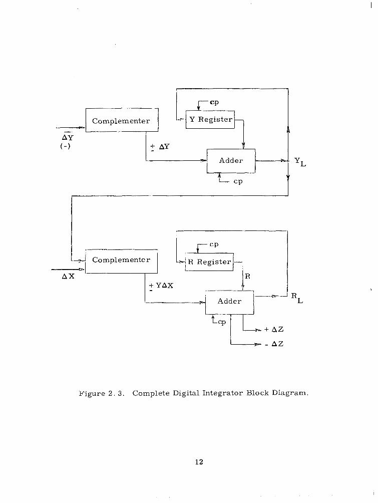
Figure 2 . 3. Complete Digital Integrator Block Diagram.
12
I
Forinstance, in the lower part of the integrator, i f Ax is present (implying a
positive value) y is passed directly through the complementer with no change.
If Ax is not present (implying a negative value) y is complemented before being
sent to the adder. To maintain synchronization of information throughout the
circuit a central source of timing pulses (indicated T in the diagram) is applied
by an external clock. The frequency of these pulses divided by the number of
bits in a word is the number of computations the integrator can perform in one
second. The present fluid digital integrator employs 5-bit words and a 100 cps
clock frequency which results in 20 iterations per second.
2.2 INTEGRATOR SUBSYSTEMS
Reference to Figure 2-2 shows that the integrator is divided into two
identical halves (excluding + - A z output channels), each of which integrate as a
function of t ime. The t ime integrators are made up of three circuits: an adder,
a complementer, and a register. The logic design for each of these three c i r -
cuits wi l l be discussed in detail in the following paragraphs.
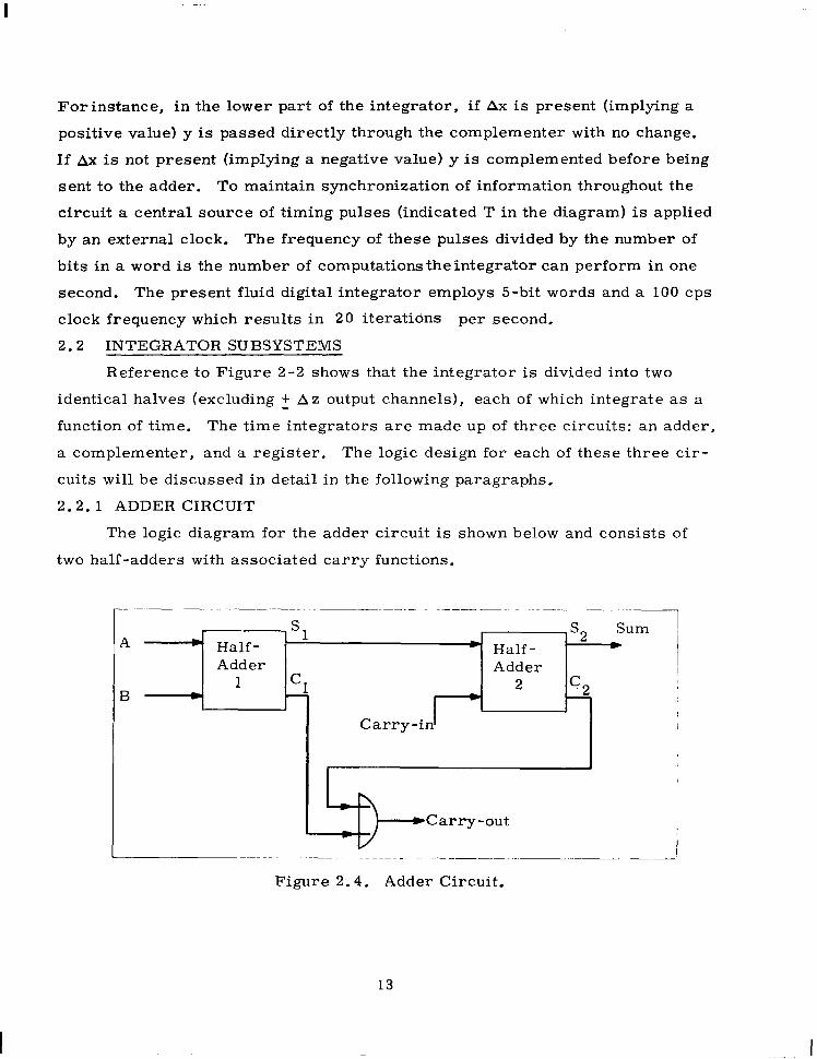
2.2.1 ADDER CIRCUIT
The logic diagram for the adder circuit is shown below and consists of
two half-adders with associated carry functions.
- "" ~ ~
A * Half- Half - Adder
1 B D 5
-
J 2 Adder
Carry-in'
3" Carry-out
I ". . ~ ~~~ ~ ..
Figure 2.4. Adder Circuit.
13
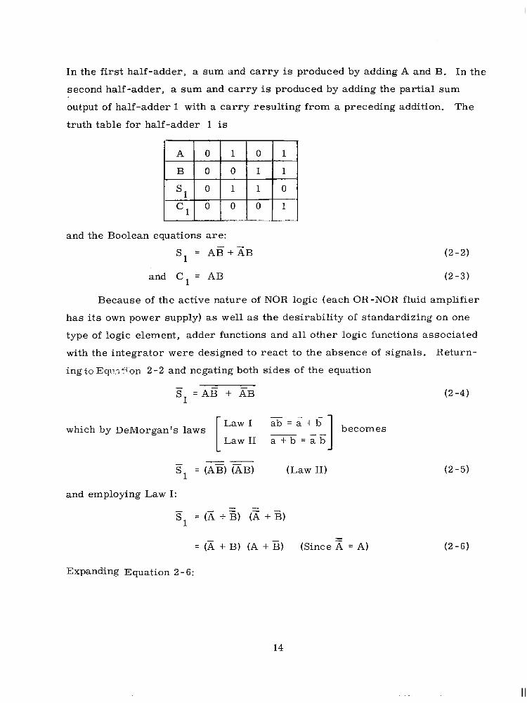
In the first half-adder, a sum and carry is produced by adding A and B. In the
second half-adder, a sum and ca r ry is produced by adding the partial sum
output of half-adder 1 with a carry result ing from a preceding addition. The
truth table for half-adder 1 is
and the Boolean equations are:
s1 = AB+XB ( 2 -2)
and C1 = AB (2 - 3 )
Because of the active nature of NOR logic (each OR-NOR fluid amplifier
has i ts own power supply) a s well as the desirability of standardizing on one
type of logic element, adder functions and all other logic functions associated
with the integrator were designed to react to the absence of signals. Return-
ing to EqusC"on 2 -2 and negating both sides of the equation - S = A B + EB
1 - "
which by DeMorgan's l a w s
"
and employing Law I: - s1 = (A + B) (A + E)
Expanding Equation 2-6:
14
"
= AB + AB
Now from Law I1
XE = A + B
and AB = AB - -
= A + B so that the negated sum is
- S l = A + B + x + B
Also from Law I, the carry (givenby Equation 2-3) is
e = A + B 1
(2-8)
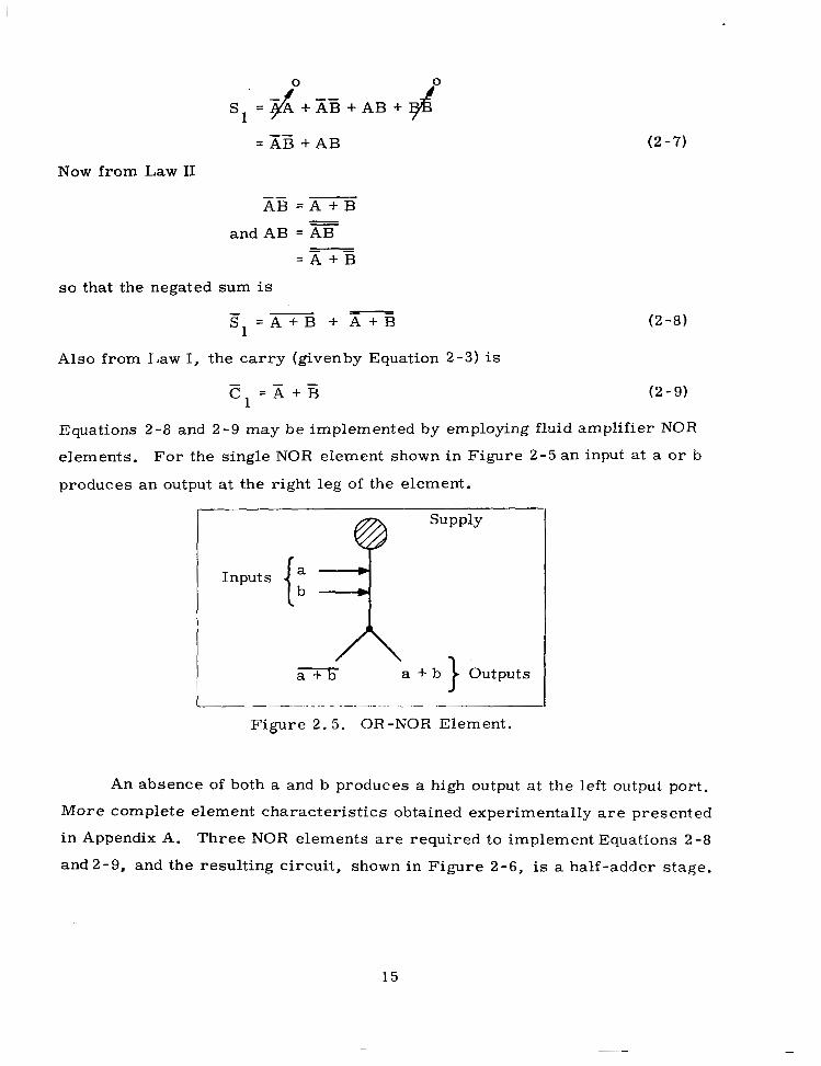
Equations 2-8 and 2-9 may be implemented by employing fluid amplifier NOR
elements. For the single NOR element shown in Figure 2-5 an input at a or b
produces an output at the right leg of the element.
a 7 a + b ) Outputs
1 -~
Figure 2.5. OR-NOR Element.
An absence of both a and b produces a high output a t the left output port.
More complete element characteristics obtained experimentally a re presented
in Appendix A. Three NOR elements are required to implement Equations 2-8
and2-9, and the resulting circuit, shown in Figure 2-6, is a half-adder stage.
15
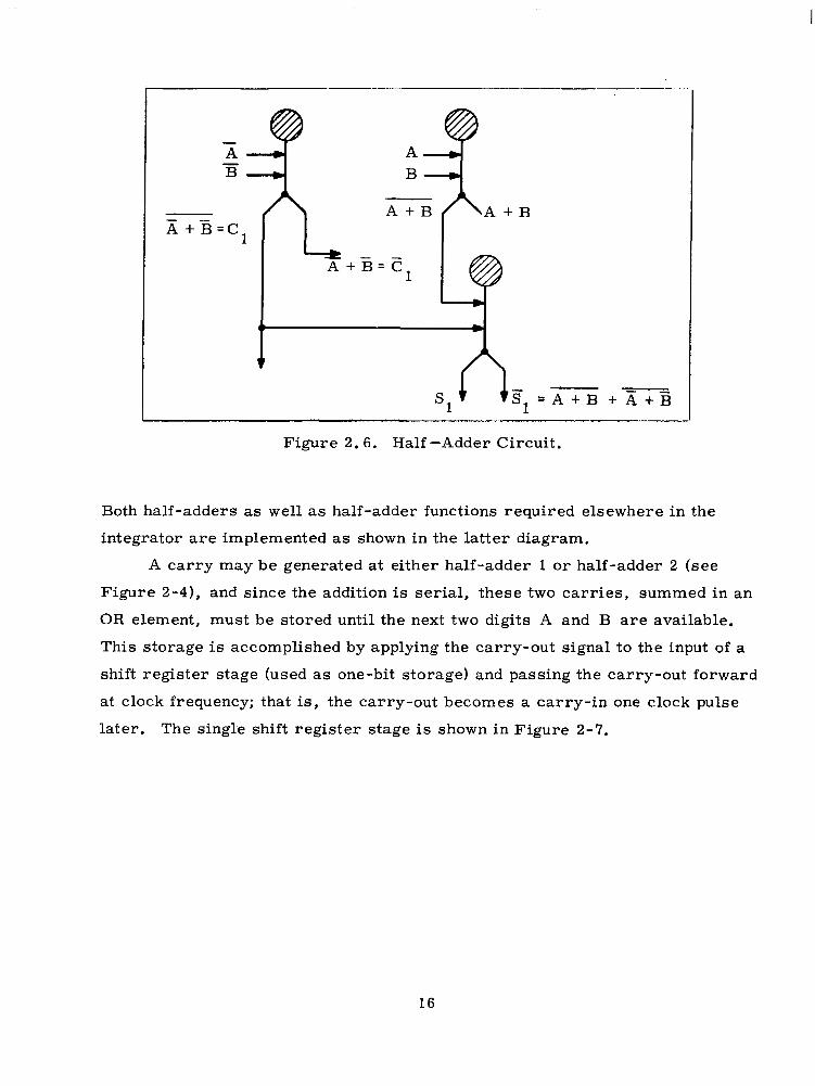
B
- A + B = C 1
A + B
*
s1 S L = A + B + A + B - "
- Figure 2 . 6 . Half -Adder Circuit.
Both half-adders as w e l l as half-adder functions required elsewhere in the
integrator are implemented as shown in the latter diagram.
A carry may be generated at either half-adder 1 or half-adder 2 (see
Figure 2-4), and since the addition is serial, these two carries, summed in an
OR element, must be stored until the next two digits A and B are available.
This storage is accomplished by applying the carry-out signal to the input of a
shift register stage (used as one-bit storage) and passing the carry-out forward
at clock frequency; that is, the carry-out becomes a carry- in one clock pulse
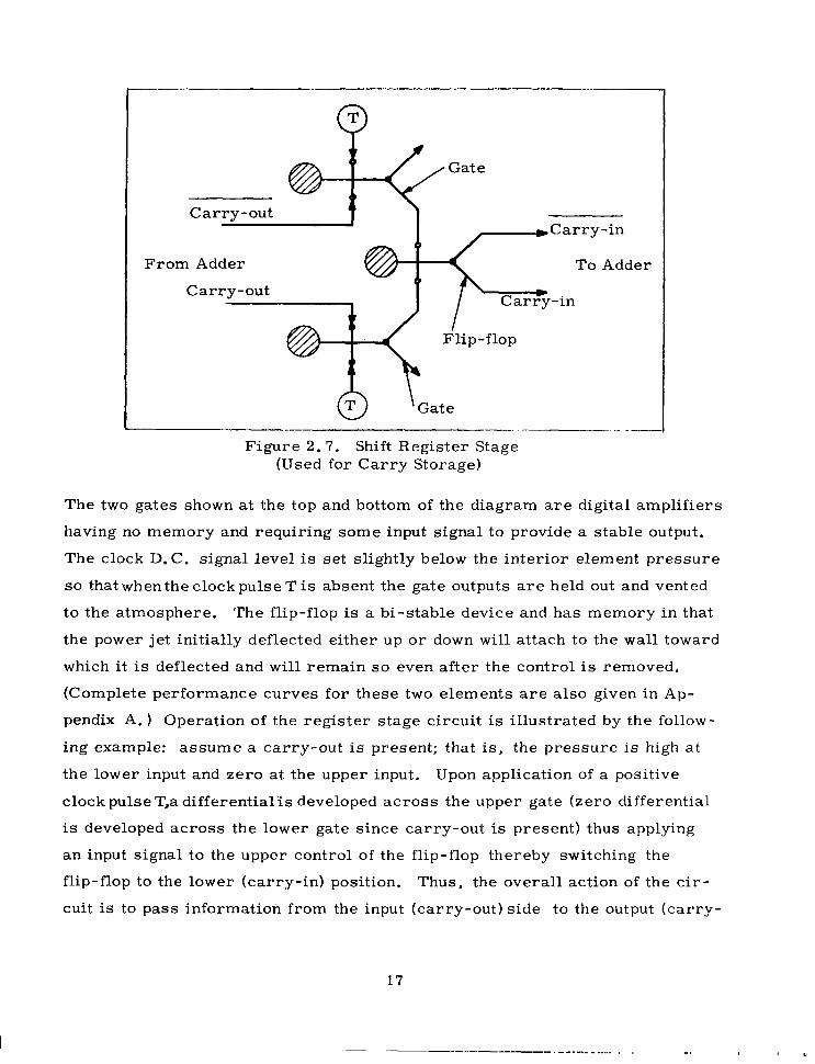
later. The single shift register stage is shown in Figure 2-7.
16
Carry-in
From Adder To Adder
-in
c " "_ . - ". ._ .___
Figure 2.7. Shift Register Stage (Used for Carry Storage)
The two gates shown at the top and bottom of the diagram are digital amplifiers
having no memory and requiring some input signal to provide a stable output.
The clock D.C. signal level is set slightly below the interior element pressure
so that whenthe clock pulse T is absent the gate outputs are held out and vented
to the atmosphere. The flip-flop is a bi-stable device and has memory in that
the power jet initially deflected either up or down w i l l attach to the w a l l toward
which it is deflected and w i l l remain so even after the control is removed.
(Complete performance curves for these two elements are also given in Ap-
pendix A. ) Operation of the register stage circuit is illustrated by the follow-
ing example: assume a carry-out is present; that is, the pressure is high a t
the lower input and zero at the upper input. Upon application of a positive
clock pulse T,a differentialis developed across the upper gate (zero differential
is developed across the lower gate since carry-out is present) thus applying
an input signal to the upper control of the flip-flop thereby switching the
flip-flop to the lower (carry-in) position. Thus, the overall action of the c i r -
cuit is to pass information from the input (carry-out) side to the output (car ry-
17
in) side on application of a clock pulse T and store thisinformation (in the state
of the flip-flop) until application of the next pulse. T.
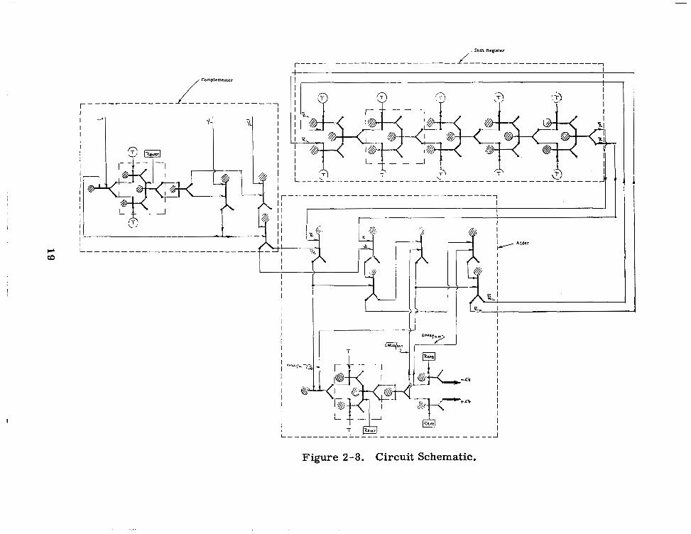
A complete adder circuit, comprising two half-adder circuits and a
register stage, is shown in the complete circuit schematic (Figure 2 - 8 ) . Discus-
sion of the operation of the overflow stage, activated by the READ pulses shown
on the diagram, w i l l be deferred until later. A s a further example of operation
of the adder, consider the timing diagram shown in Figure 2 - 9 and assume the
numbers A = 5 and B = 2 1 are to be added. Prior to T (the first clock pulse)
A and B produce a zero output of R and a carry-out; application of T passes L the carry forward to the carry-in position where it is combined with zero
inputs from A and B to produce a high output at R The rest of the addition
proceeds from T through T5 in direct analogy to the binary addition shown
above the timing diagram. In an actual test of equipment the numbers A and B
were generated with a pneumatic signal generator consisting of a binary coded
disk rotating in synchronization with the clock frequency. This equipment is
described in Section 3 .
2 . 2 . 2 COMPLEMENTER OPERATION
1
L'
1
If a subtract signal is present, the subtrahend is complemented and then
added to the minuend, If a substract signal is absent (implying addition) the
number is passed unmodified through the complementer. As shown previously
(Section 2. l ) , to form the two's complement all leading zeros as w e l l as the
first one of the subtrahend are passed intact. Then all succeeding digits are
inverted. Thus the logical requirements of the complementer can be sum-
marized as shown in Figure 2 - 1 0 . E is assumed to be the number passing
into the complement er.
18
,, Complcrncnter
""_"""" I """"""_ I
1 ""_"""""""""" I """"""_"""" t- I I I
I
I I
I ! t I +- I .,;
T & I I I
L - _ - _ _ _ _ _ _ _ 1 _ _ _ _ _ _ _ _ _ _ _ _ _ - _ _ _ _ ____" I
Figure 2-8. Circuit Schematic.
I I I I I
I I
I I I
Carry in 1 1
A (=5) 0 0 1 0 1
B ( = 2 1 ) 1 0 1 0 1
R L ( = 2 6 ) 1 1 0 1 0
B I I //t Carry out
i
Carry in I 1 I I R L R
T1 T2 T3 T4 T5
Time
Figure 2 . 9 . Adder Timing Diagram
2 0
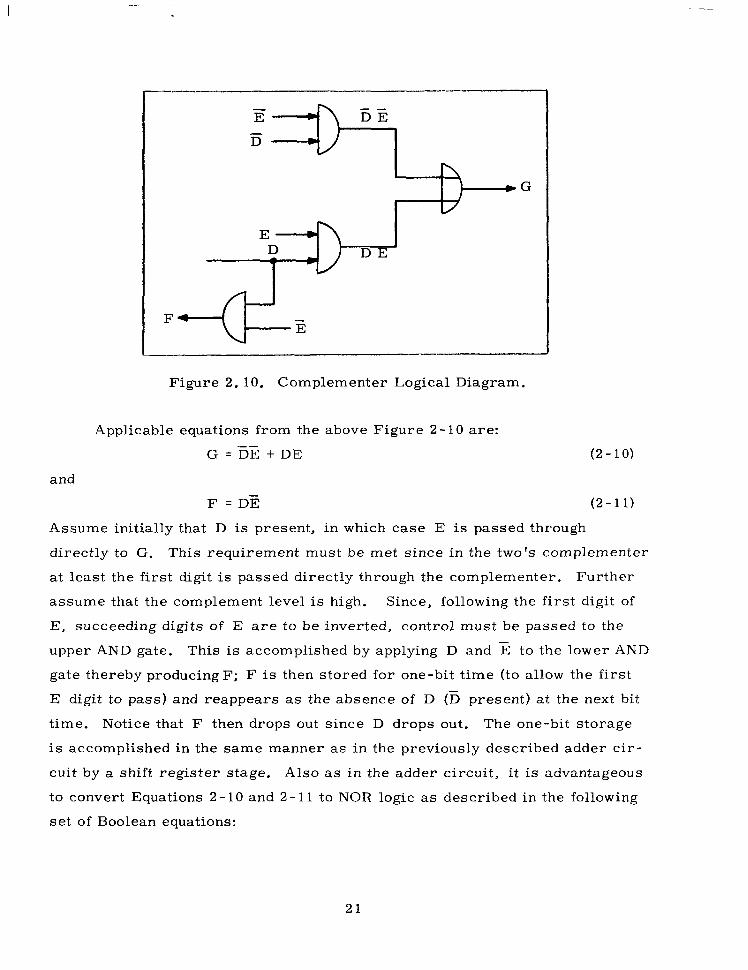
Figure 2. 10. Complementer Logical Diagram.
Applicable equations from the above Figure 2 - 10 a re :
G =E% + D E
and
F = DZ
(2 -10)
(2 - 11)
Assume initially that D is present, in which case E is passed through
directly to G. This requirement must be met since in the two's complementer
at least the f irst digit is passed directly through the complementer. Further
assume that the complement level is high. Since, following the first digit of
E, succeeding digits of E are to be inverted, control must be passed to the
upper AND gate. This is accomplished by applying D and E to the lower AND
gate thereby producing F; F is then stored for one-bit time (to allow the first
E digit to pass) and reappears as the absence of D (5 present) a t the next bit
time. Notice that F then drops out since D drops out. The one-bit storage
is accomplished in the same manner as in the previously described adder cir-
cuit by a shift register stage. Also as in the adder circuit, it is advantageous
to convert Equations 2 - 10 and 2 - 11 to NOR logic as described in the following
se t of Boolean equations:
21
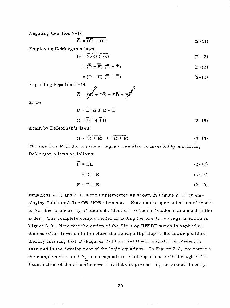
Negating Equation 2 - 10 - G =DE +DE
Employing DeMorgan's la,ws - " G = (ZE) (DE)
= (D + E) (5 + E) Expanding Equation 2 - 14
0
E=I#+D*:+13E+$o
Since -
D = D a n d E = * : ..
(2- 11)
(2-12)
(2-13)
( 2 - 14)
(2-15)
Again by DeMorgan's laws - G = (5 + E) + (D + E) (2 -16)
The function F in the previous diagram can also be inverted by employing
DeMorgan's l a w s as follows:
F = DE I -
( 2 - 17) -
= D + E - (2 - 18)
- F = E + E (2-19)
Equations 2 - 16 and 2 - 19 were implemented as shown in Figure 2 - 11 by em-
ploying fluid amplifier OR-NOR elements. Note that proper selection of inputs
makes the lat ter array of elements identical to the half-adder stage used in the
adder. The complete complementer including the one-bit storage is shown in
Figure 2-8. Note that the action of the flip-flop RESET which is applied at
the end of an i teration is to return the storage flip-flop to the lower position
thereby insuring that D (Figures 2 - 10 and 2-11) w i l l initially be present as
assumed in .the development of the logic equations. In Figure 2-8, Ax controls
the complementer and Y corresponds to E of Equations 2 - 10 through 2 - 19.
Examination of the circuit shows that i f Ax is present Y is passed directly L
L
22
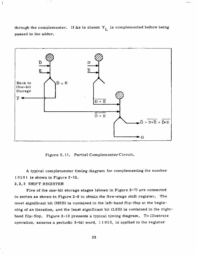
through the complementer. If Ax is absent YL is complemented before being
passed to the adder.
J.
. E Back to A D -t One-bit Storage
F -
Figure 2.11. Partial Complementer Circuit .
A typical complementer timing diagram for complementing the number
1 0 10 1 is shown in Figure 2- 12.
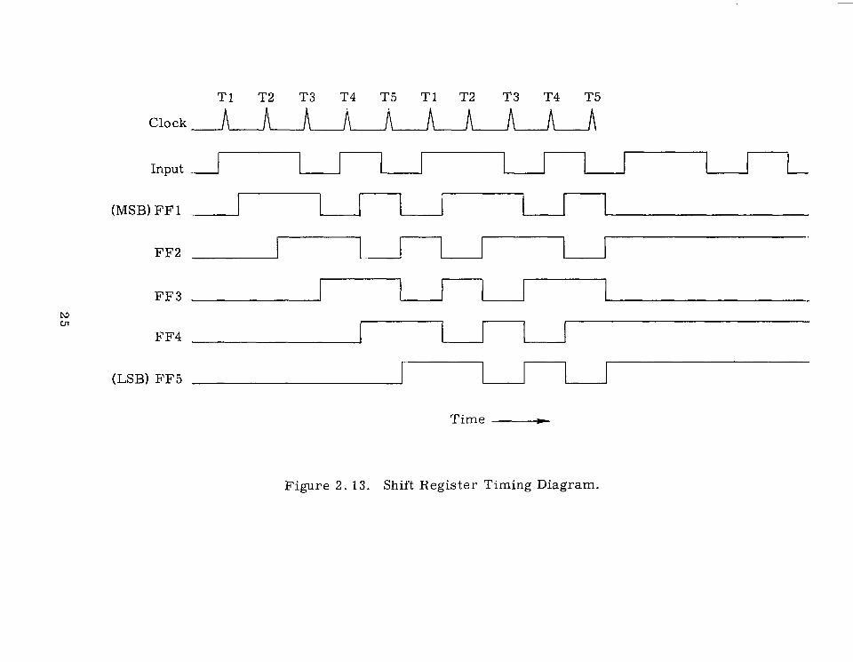
2.2.3 SHIFT REGISTER
Five of the one-bit storage stages (shown in Figure 2-7) a r e connected
in se r ies as shown in Figure 2-8 to obtain the five-stage shift register. The
most significant bit (MSB) is contained in the left-hand flip-flop at the begin-
ning of an iteration, and the least significant bit (LSB) is contained in the right-
hand flip-flop. Figure 2-13 presents a typical timing diagram. To illustrate
operation, assume a periodic 5-bit word, 1 1 01 0, is applied to the register
23
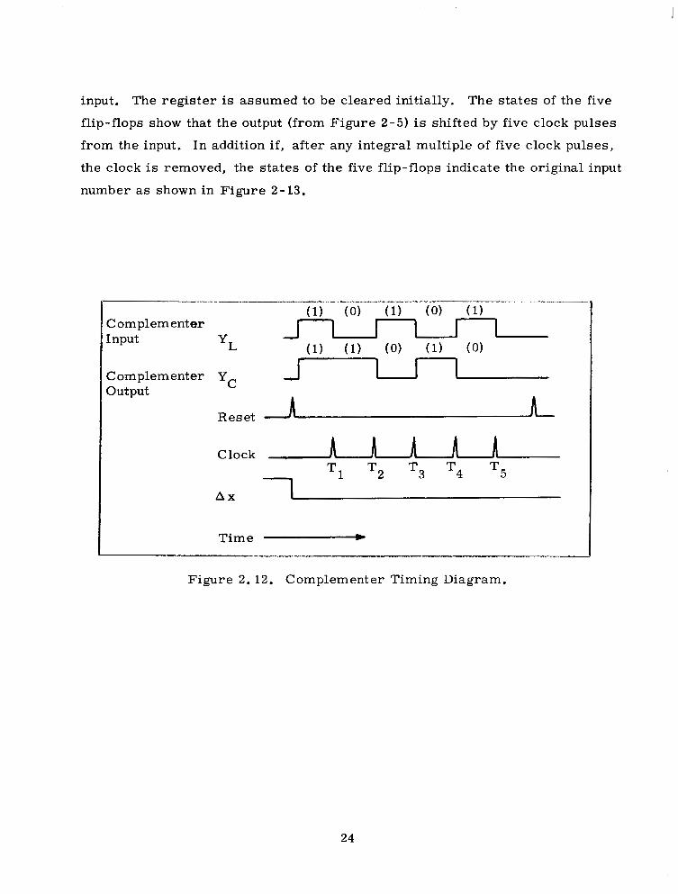
input. The register is assumed to be cleared initially. The states of the five
flip-flops show that the output (from Figure 2-5) is shifted by five clock pulses
from the input. In addition i f , after any integral multiple of five clock pulses,
the clock is removed, the states of the five flip-flops indicate the original input
number as shown in Figure 2-13.
~
Clock AIAAA T1 T2 T3 T4 T5 1
A x I
I Time - Figure 2. 12. Complementer Timing Diagram.
24
1-1 ~2 T3 T4 T5 T1 T2 T3 T4 T5
Clock A A A
Input . I J I (MSB) FF1 .. 1
FF3 I 1 1 FF4 I
(LSB) FF5 1 I 1 I Time -
Figure 2 . 13. Shift Register Timing Diagram.
2 . 3 INTEGRATOR OPERATION
As previously outlined, the integrator operates by receiving an input
Y at the complementer, If Ax is absent Y is complemented; i f Ax is
present Y is passed directly to the adder. At the adder the remainder of a
previous addition and the latest value of Y are summed, producing a new
remainder and a value of Az (a change in the value of the integral).
L L
L
C
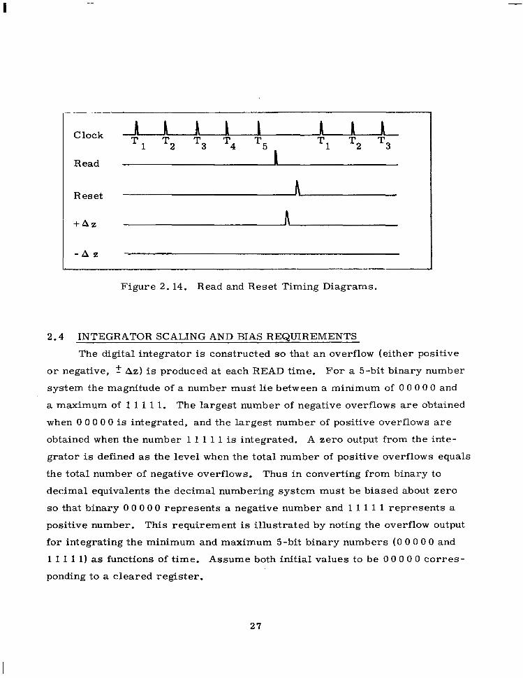
Operation of the adder reset and overflow stage now can be illustrated.
Assume as an example that the two numbers Y = 2 0 (1 0 1 0 0) and RL = 30
(1 1 1 1 0) are to be summed. The addition wi l l produce the value 50 which is
too large to be contained as a five-bit number, and a sixth bit wi l l be formed;
C
this bit wil l be sensed as overflow and of course has the binary value 32, i. e.,
1 0 1 0 0 (Y,) 1 1 1 1 0 (RL)
1 1 0 0 1 0 "
Overflow Remainder
The presence of an overflow is sensed by determining if a carry has occurred
after the addition of the fifth and most significant bits (occurs at the fifth clock
pulse). The sensing is done by applying READ pulses on two shift register
gates driven by the carry signal (see Figure 2 - 8 ) . The READ pulses are
applied only after each fifth clock pulse so that only carry pulses with a value
of 32, i. e. , overflows, are sensed. Since each bit generated by the adder is
normally sent back to the register to be employed as remainder in a succeeding
iteration, the flip-flop which generates an overflow must be reset to zero before
the next iteration commences. Operation of the over€low stage is similar to
that previously described for the shift register in that the two gates shown are
held open until a READ pulse is applied. A timing diagram, illustrating the
operation of the READ and RESET signals is shown in Figure 2 - 14. Note that
the overflow wi l l always be either positive or negative and never zero.
26
Clock A L b 1, I )r I )i T 1 T2 T3 T4 T5 - T1 T2 T3
Read I
Reset
+ A z A
A
- A z . " ..
Figure 2.14. Read and Reset Timing Diagrams.
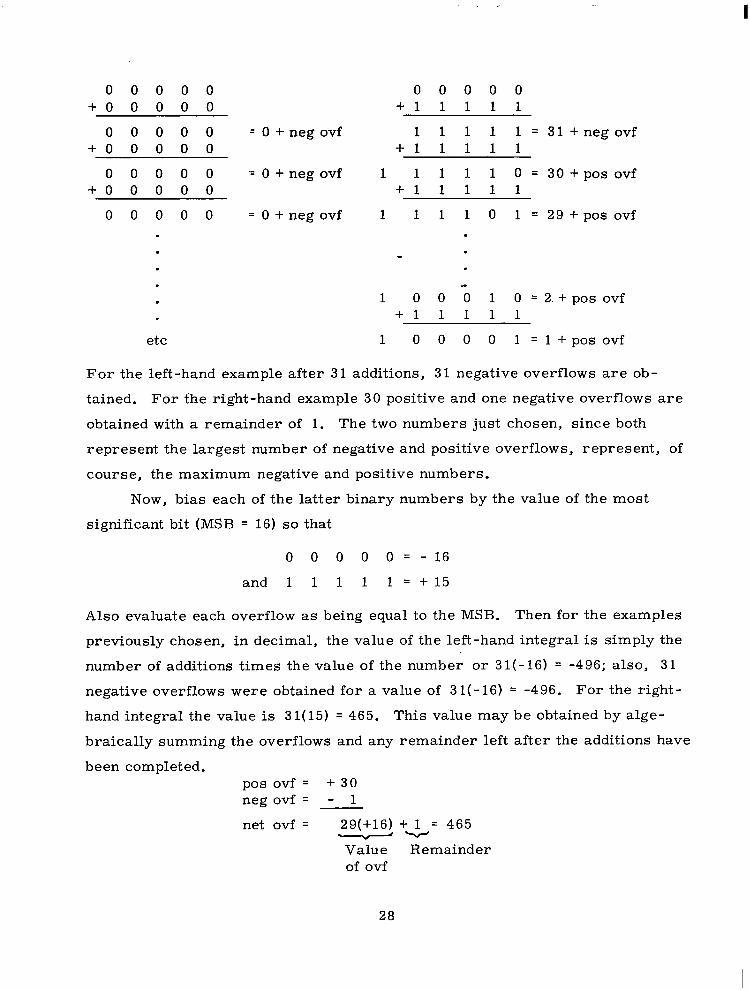
2.4 INTEGRATOR SCALING AND BIAS REQUIREMENTS
The digital integrator is constructed so that an overflow (either positive
o r negative, f Az) is produced at each READ time. For a 5-bit binary number
system the magnitude of a number must lie between a minimum of 0 0 0 0 0 and
a maximum of 1 1 1 1 1. The largest number of negative overflows are obtained
when 0 0 0 0 0 is integrated, and the largest number of positive overflows a r e
obtained when the number 1 1 1 1 1 is integrated. A zero output from the inte-
grator is defined as the level when the total number of positive overflows equals
the total number of negative overflows. Thus in converting from binary to
decimal equivalents the decimal numbering system must be biased about zero
so that binary 0 0 0 0 0 represents a negative number and 1 1 1 1 1 represents a
positive number. This requirement is illustrated by noting the overflow output
for integrating the minimum and maximum 5-bit binary numbers ( 0 0 0 0 0 and
1 1 1 1 1) as functions of time. Assume both initial values to be 0 0 0 0 0 co r re s -
ponding to a cleared register.
27
I
0 0 0 0 0 + o o o o o
0 0 0 0 0 + o o o o o
0 0 0 0 0 + 1 1 1 1 1
= 0 + neg ovf 1 1 1 1 1 = 31 + neg ovf + 1 1 1 1 1
0 0 0 0 0 + o o o o o
= 0 + neg ovf 1 1 1 1 1 0 = 30 + pos ovf + 1 1 1 1 1
0 0 0 0 0 = 0 + neg ovf 1 1 1 1 0 1 = 29 + pos ovf
1 0 0 0 1 0 = 2. + pos ovf I
+ 1 1 1 1 1
et c 1 0 0 0 0 1 = 1 + p o s ovf
For the left-hand example after 31 additions, 31 negative overflows are ob-
tained. For the right-hand example 30 positive and one negative overflows are
obtained with a remainder of 1. The two numbers just chosen, since both
represent the largest number of negative and positive overflows, represent, of
course, the maximum negative and positive numbers.
Now, bias each of the lat ter binary numbers by the value of the most
significant bit (MSB = 16) so that
0 0 0 0 O = - 1 6
and 1 1 1 1 1 = + 1 5
Also evaluate each overflow as being equal to the MSB. Then for the examples
previously chosen, in decimal, the value of the left-hand integral is simply the
number of additions times the value of the number o r 31(-16) = -496; also, 31
negative overflows were obtained for a value of 31(-16) = -496. For the right-
hand integral the value is 3 1( 15) = 465. This value may be obtained by alge-
braically summing the overflows and any remainder left after the additions have
been completed. pos ovf = + 30 neg ovf = - 1
net ovf = 29(+16) + 1 = 465 " Value Remainder of ovf
28
I
In a practical application, since it is inconvenient to inspect the remain-
der contained within the shift register, a particular problem should be scaled
.to produce a rapid overflow rate, thereby making the register contents small
compared with the number of overflows (recall that two overflows are equiva-
lent to the entire contents of the register).
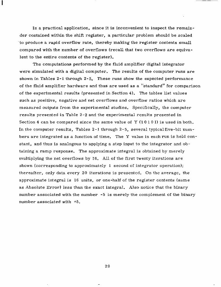
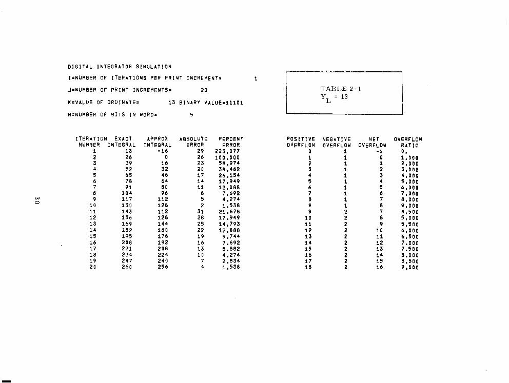
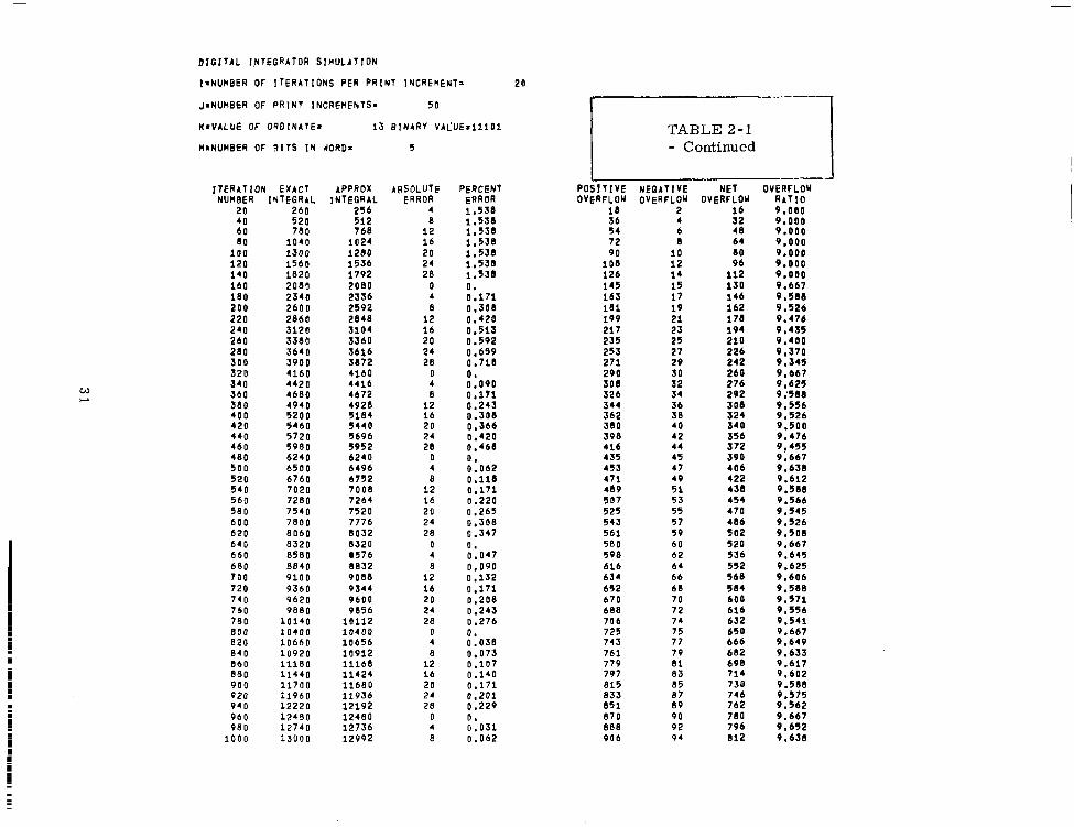
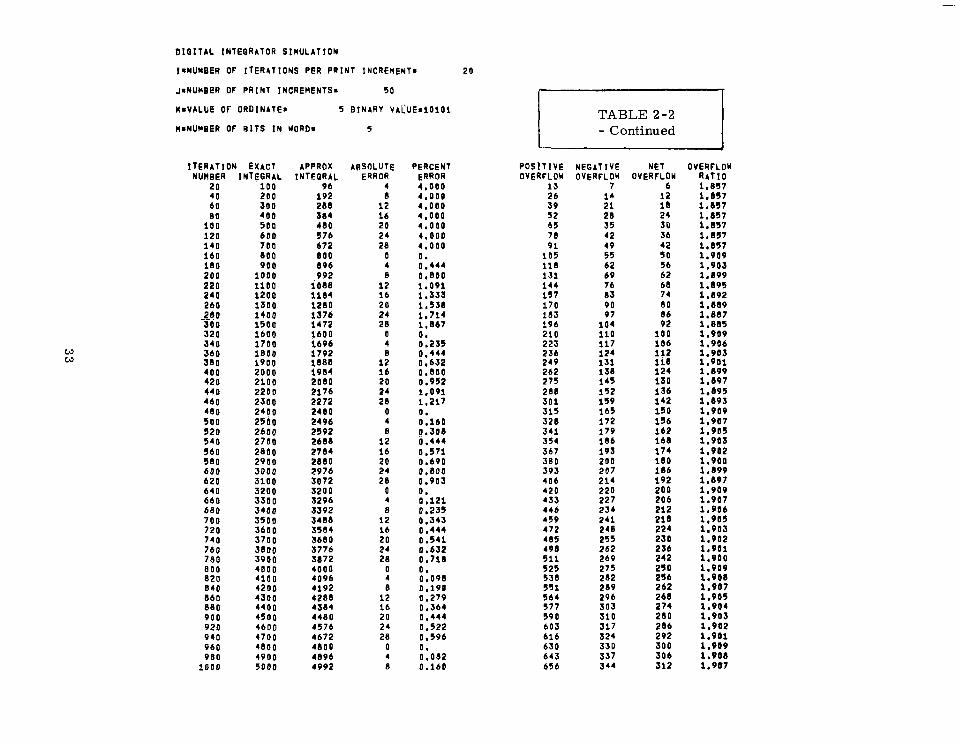
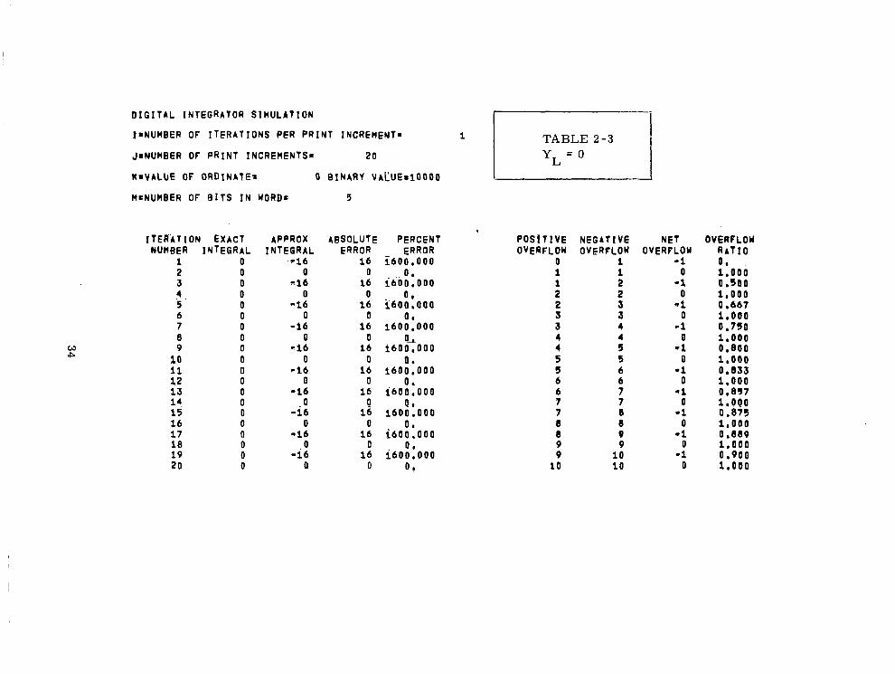
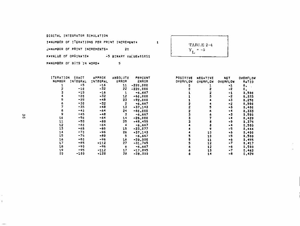
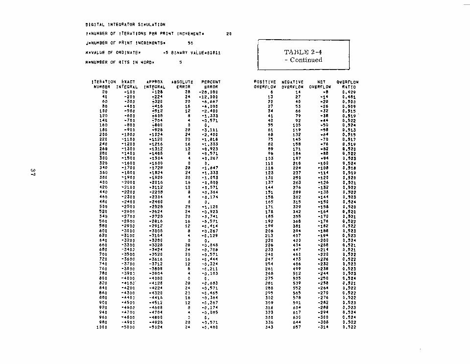
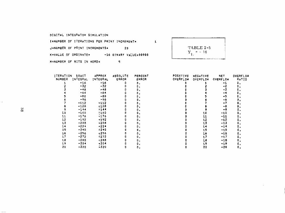
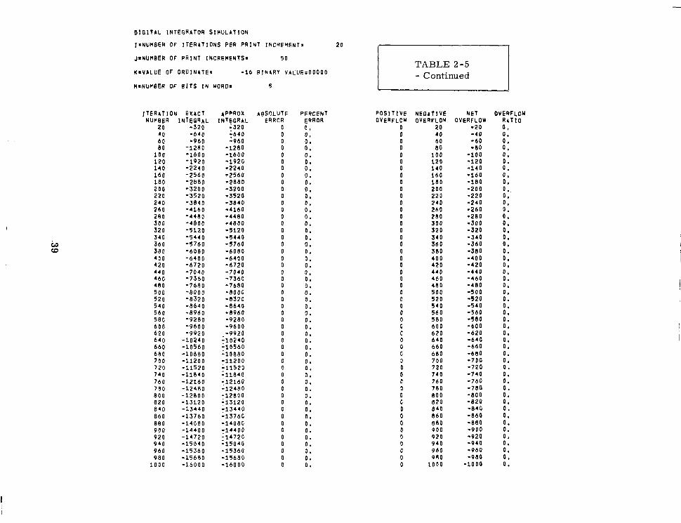
The computations performed by the fluid amplifier digital integrator
were simulated with a digital computer. The results of the computer runs are
shown in Tables 2- 1 through 2- 5, These runs show the expected performance
of the fluid amplifier hardware and thus are used as a "standard" for comparison
of the experimental results (presented in Section 4). The tables list values
such as positive, negative and net overflows and overflow ratios which are
measured outputs from the experimental studies. Specifically, the computer
results presented in Table 2 -2 and the experimental results presented in
Section 4 can be compared since the same value of Y (1 0 1 0 1) is used in both.
In the computer results, Tables 2-1 through 2-5, several typical five-bit num-
be r s are integrated as a function of time. The Y value in each run is held con-
stant, and thus is analogous to applying a step input to the integrator and ob-
taining a ramp response. The approximate integral is obtained by merely
multiplying the net overflows by 16. All of the first twenty iterations are
shown (corresponding to approximately 1 second of integrator operation);
thereafter, only data every 20 iterations is presented. On the average, the
approximate integral is 16 units, o r one-half of the register contents (same
as Absolute Error) less than the exact integral. Also notice that the binary
number associated with the number -5 is merely the complement of the binary
number associated with +5.
2 9
W 0
D I G I T A L INTEGRATOR SIMULATION
!=NUMBER OF ITERATIONS PER PRIYT INCREMENT=
JZNUMeER OF PRINT INCREMENTS- 20
KrVALUE OF O R D I N A T E = 1 3 B I N A R Y V A L U E n l l l O l
H=NUMOER OF S I T S I N W O R D = 5
ITER4TION EXACT
1 13 2 3
26 3 9
4 5 2 5 6 5 6 7 8 7 9 1 8 1 0 4 9 1 1 7
1 0 1 3 0 11 1 4 3 1 2 1 5 6 13 1 6 9 1 4 1 8 2 1 5 1 9 5 1 6 2 0 8 1 7 2 2 1 18 2 3 4 19 2 4 7 20 260
NUM9ER INTEGRAL APPROX
INTEGRAL - 1 6
0 1 6 3 2 4 8 6 4 80 9 6
1 1 2 1 2 8 1 1 2 1 2 8 1 4 4 1 6 0 1 7 6 1 9 2 2 0 8 2 2 4 2 4 0 2 5 6
ABSOLUTE E R R O R
2 9 26 23 20 17 1 4 11
8 5 2
31 28 25 2 2 1 9 16 1 3 10
7 4
PERCENT FRROR
2 2 3 , 0 7 7 1 0 0 . 0 0 0
5 0 , 9 7 4 3 8 , 4 6 2 2 6 . 1 5 4 1 7 , 9 4 9 1 2 . 0 8 8
7 , 6 9 2 4 , 2 7 4 1 . 5 3 8
2 1 . 6 7 8 1 7 . 9 4 9 1 4 , 7 9 3 12.088
9 . 7 4 4 7 . 6 9 2 5 . 8 8 2 4 . 2 7 4 2 , 8 3 4 1 . 5 3 8
1 1
TABLE 2 - 1 YL = 13 TABLE 2 - 1 YL = 13
P O S I T I V E OVERFLOW
0 1 2 3 4 5 6 7 8 9 9
1 0 11 1 2 13 1 4 1 5 16 17 1 8
NEGATIVE OVFRFLOW
1 1 1 1 1 1 1 1 1 1 2 2 2 2 2 2 2 2 2 2
NET OVERFLOY
-1 0 1 2 3 4 5 6 7 8 7 8 9
10 11 1 2 13 1 4 1 5 1 6
OVERFLOW R 4 7 1 0 0 , 1 . 0 0 0 2 . 0 0 0 3 , 0 0 0 4 , 0 0 0 5 . 0 0 0 6 , 0 0 0 7 . 0 0 0 8 . 0 0 0 9 . 0 0 0 4 . 5 0 0 5 . 0 0 0 5 .500 6 . 0 0 0 6 . 5 0 0 7 . 0 0 0 7 . 5 0 0 8 . 0 0 0 8 . 5 0 0 9 , 0 0 0
DIGITAL I.NTEGRATOR SIHULATION
ISNUWEER OF 1TERATIONS PER PRINT INCREMENT=
JaNUHBER OF PRINT INCREHENTS. 50
KIVALUE O F ORDINATE* 1 3 BlNlRY V A ~ U E r I l l O l
HaNUHBER OF RlTS I N U O R D a
I T E R A T I O N EXACT NUH8ER
20 40
80 1 0 0 1 2 0 1 4 0 160 1 8 0
2 2 0 2 0 0
2 4 0 2 6 0 2 8 0 3 0 0
3 4 0 3 2 0
3 6 0 3 8 0 4 0 0 4 2 0
4 6 0 4 4 0
4 8 0 5 0 0 5 2 0 5 4 0
5 8 0 5 6 0
6 0 0 6 2 0 6 4 0 660 6 8 0 700 720 740 760 780 8 0 0 8 2 0 8 4 0 8 6 0
9 2 0 9 0 0
9 4 0 9 6 0
1 0 0 0 9 8 0
60
eeo
INTEGRAL 2 6 0 5 2 0 7 8 0
1 0 4 0 1300 1 5 6 0 1 8 2 0 2 0 8 1 2 3 4 0 2 6 0 0 2 8 6 0 3 1 2 0 3380 3 6 4 0 3 9 0 0 4 1 6 0 4 4 2 0 4 6 8 0 4 9 4 0 5 2 0 0 5 4 6 0 5 7 2 0 5 9 8 0 6 2 4 0 6 5 0 0 6 7 6 0 7 0 2 0 7 2 8 0 7 5 4 0 7 8 0 0 8 0 6 0 8 3 2 0 8580 8 8 4 0 9 1 0 0 9 3 6 0 9 6 2 0 9880
1 0 4 0 0 1 0 6 6 0 1 0 9 2 0 1 1 1 8 0 1 1 4 4 0 1 1 7 0 0 1 1 9 6 0 1 2 2 2 0 1 2 4 9 0 1 2 7 4 0 1 3 0 0 0
10140
INTEGRAL APPRDX
2 5 6 5 1 2
1 0 2 4 1 6 8
1 2 8 0 1 5 3 6 1 7 9 2 2 0 8 0 2 3 3 6 2 5 9 2 2 8 4 8 3 1 0 4 3 3 6 0 5 6 1 6 3 8 7 2
4 4 1 6 4 1 6 0
4 6 7 2 4 9 2 8 5 1 8 4 5 4 4 0
5 9 5 2 5 6 9 6
6 2 4 0 6 4 9 6 6’152 7 0 0 8
7 5 2 0 7 2 6 4
7 7 7 6 8 0 3 2 8 3 2 0 8 5 7 6
9088 8 8 3 2
9 3 4 4 9 6 0 0 9 8 5 6
1 0 1 1 2 1 0 4 0 0 1 0 6 5 6 1 0 9 1 2 1 1 1 6 8 1 1 4 2 4 1 1 6 8 0 11936 1 2 1 9 2 1 2 4 8 0 1 2 7 3 6 1 2 9 9 2
5
ARSDLUTE E R R O R
4
1 2 8
16 20 24 28 0 4 8
1 2 16 20 24 28
0 4
1 2 8
1 6 20 24 28
4 0
1 2 8
16 20 24 28
4 0
1 2 8
1 6 2 0 24 28 0 4
1 2 8
1 6
24 2 0
2 8 0 4 8
PERCENT ERROR 1 . 5 3 8 1 . 5 3 8 1 , 5 3 8
1 . 5 3 8 1 . 5 3 8
1 . 5 3 8 1 . 5 3 8 0 . 0 . 1 7 1 0 . 3 0 8
0.513 0 . 5 9 2 0 . 6 3 9 0 . 7 1 8
0 . 0 9 0 0 .
0 . 1 7 1 0 . 2 4 3 0 .308 0 . 3 6 6
0 . 4 6 8 0 . 0 . 0 6 2 0.118 0 . 1 7 1
0 . 2 6 5 0 . 2 2 0
0 . 3 0 8 0 . 3 4 7 0. 0 . 0 4 7
0 . 1 3 2 0 , 0 9 0
0 . 1 7 1 0 . 2 0 8 0 . 2 4 3 0 . 2 7 6 0. 0 . 0 3 8 0 . 0 7 3 0 . 1 0 7
0 . 1 7 1 0 . 2 0 1
0. 0 . 0 3 1 0 . 0 6 2
0 . 4 2 0
0 . 4 2 0
0 . 1 4 0
0 . 2 2 9
20
7---”l TABLE 2 - 1 - Continued
P O S I T I V E OVERFLOW
18 3 6 5 4
9 0 7 2
1 0 8 1 2 6 1 4 5 163
1 9 9 1 8 1
2 1 7 2 3 5 2 5 3 2 7 1
308 2 9 0
3 2 6 3 4 4 3 6 2 380 3 9 8 4 1 6 4 3 5 4 5 3 4 7 1 4 8 9 5 0 7 5 2 5 5 4 3 5 6 1 580 5 9 8 6 1 6 6 3 4 65 2 6 7 0 6 8 8 7 0 6
7 4 3 7 2 5
7 6 1 7 7 9 7 9 7 8 1 5 033 8 5 1 8 7 0 888 9 0 6
NEGATIVE OVERFLOW
2 4 6 8
10 1 2
15 1 7 1 9 2 1 23 25 27 2 9
3 2 3 0
34 3 6 3 8 4 0
44 42
45 47 49 5 1
5 5 53
5 7 5 9 60 6 2
6 6 64
6 8 70 7 2 74
7 7 75
7 9 8 1 83 85
8 9 8 7
90 9 2 9 4
1 4
OVERFLOU NET
16 3 2 48 64 80
1 1 2 9 6
130 1 4 6 162 178 1 9 4 2 1 0 2 2 6 2 4 2
2 7 6 2 6 0
2 9 2 308 524 3 4 0
3 7 2 3 5 6
3 9 0 4 0 6 4 2 2 4 3 8
4 7 0 4 5 4
486 5 0 2 5 2 0 5 3 6
5 6 8 5 5 2
S84 600 6 1 6 6 3 2
6 6 6 650
6 8 2 6 9 8 7 1 4 7 3 0 7 4 6 7 6 2 780 7 9 6 8 1 2
OVERFLOU RATIO 9.000 9 . 0 0 0 9 . 0 0 0 9 . 0 0 0
9 . 0 0 0 9 . 0 0 0 9 . 6 6 7 9 . 5 8 8 9 . 5 2 6 9 .476 9 . 4 3 5 9 .400 9 . 5 7 0 9 . 3 4 5
9 . 6 2 5 9 . 6 6 7
9 i 5 8 8 9 , 5 5 6 9 . 5 2 6 9 . 5 0 0 9 . 4 7 6 9 4 5 5 9 . 6 6 7 9.638 9 . 6 1 2 9 . 5 8 8
9 . 5 4 5 9 . 5 6 6
9 . 5 2 6 9 . 5 0 8 9 . 6 6 7 9 , 6 4 5
9 . 6 0 6 9 . 6 2 5
9 . 5 8 8 9.571 9 , 5 5 6 9 . 5 4 1
9 , 6 4 9 9 . 6 6 7
9 . 6 3 3 9 . 6 1 7 9 . 6 0 2 9 . 5 8 8
9 . 5 6 2 9 .575
9 . 6 6 7 9 . 6 5 2 9.638
9.000
W Po
D I G I T A L INTEGRATOR SIMULATION
IaNUHBER OF ITERATIONS PER PRINT INCREMENT.
JINUMBER OF PRINT INCREMENTS= 2 0
KaVALUE OF ORUINAlEa 5 BINARY VALUE=lOlOl
H=NUHBER OF B I T S I N W O R D = 5
ITERATION EXACT
1 5 2 1 0 3 1 5 4 20 5 25 6 30 7 35 8 40 9 45
10 5 0 11 55 1 2 60 1 3 65 14 70 1 5 7 5 1 6 8 0 1 7 8 5 1 8 9 0 1 9 9 5 20 1 0 0
NUMBER INTEGRAL APPROX
INTEGRAL - 1 6
0 - 1 6
0 1 6
0 1 6 3 2 1 6 32 48 3 2 48 64 48 64 80 64 80 9 6
ABSOLUTE ERROR
2 1 10 3 1 20
9 30 1 9
8 29 1 8
7 28 1 7
6 2 7 1 6
5 26 1 5
4
PERCENT ERROR
420.000 ioo..q.qo 206.667 100.000
36,000 100.000
54 , 2 8 6 20,ooo 64.444 36.000 12 ,727 46.667 26,154
8 , 5 7 1 36.000 20.000
5 ,882 28.889 1 5 7 8 9
4.000
7". i 1 I TABLE 2-2 i
POS!TIVE OVERFLOW
0 1 1 2 3 3 4 5 5 6 7 7 8 9 9
1 0 11 11 1 2 1 3
NEGATIVE OVERFLOW 1
1 2 2 2 3 3 3 4 4 4 5 5 5 6 6 6 7 7 7
NET OVERFLOY
-1 0
-1 0 1 0 1 2 1 2 3 2 3 4 3 4 5 4 5 6
OVERFLOW RATIO 0 . 1 . 0 0 0 0 , 5 0 0 1,000 1.500 1,000 1.333 1,667 1.250 1 ,500 1,750 1,400 1.600 1,800 1.500 1,667 1.833
1.714 1 . 5 7 1
1 e 8'57
w W
D I G I T A L I N T E G R A T O R S I M U L A T I O N
ISNUMBER OF ITERATIONS P E R P R I N T I N C R E M E N T S
JsNUHBER OF P R I N T I N C R E W E N T S a 50
KSVALLIE OF O R D I N A T E S 5 B I N A R Y V A C U E S l O l O l
HaNUMBER OF R I T S I N WORD.
ITERATION E X A C T NUMBER
2 0 40 60
1 0 0 80
1 2 0 1 4 0 160 180 2 0 0 2 2 0 2 4 0 2 6 0 " 2 8 0 3 0 0 3 2 0 3 4 0
380 3 6 0
4 0 0 4 2 0 4 4 0
5 0 0 480
5 2 0 5 4 0 5 6 0 5 8 0
6 2 0 6 0 0
6 4 0 660 6 8 0 7 0 0 7 2 0 7 4 0 7 6 0 7 8 0 8 0 0 820 8 4 0 860 880 9 0 0 9 2 0 9 4 0 9 6 0
1 0 0 0 9 8 0
4 6 0
INTEGRAL 1 0 0 2 0 0
4 0 0 3 0 0
5 0 0 600 7 0 0 800 9 0 0
1 0 0 0 1 1 0 0 1 2 0 0 1 3 0 0 1 4 0 0 1 5 0 0 1 6 0 0 1 7 0 0 1 8 0 0 1 9 0 0 2 0 0 0 2 1 0 0 2 2 0 0 2 3 0 0
2600 2 5 0 0
2 7 0 0 2 8 0 0 2 9 0 0 3000 3 1 0 0 3 2 0 0 3300 3 4 0 0 3 5 0 0 3600
3800 3 7 0 0
3 9 0 0 4 0 0 0 4 1 0 0 4 2 0 0 4 3 0 0 4 4 0 0 4 5 0 0 4 6 0 0 4 7 0 0 4 8 0 0 4 9 0 0 5 0 0 0
2 4 0 0
I N T C Q R A L APPROX
1 9 2 9 6
2 8 8 3 8 4 4 8 0 5 7 6 6 7 2 800 8 9 6 9 9 2
1088 1 1 8 4 1280 1 5 7 6 1 4 7 2 1 6 0 0 I 6 9 6 1 7 9 2 1888 1 9 8 4 2 0 8 0 2 1 7 6 2 2 7 2 2 4 0 0 2 4 9 6 2 5 9 2 2 6 8 8 2 7 8 4 2 8 8 0 2 9 7 6 3 0 7 2 3 2 0 0 3 2 9 6 3 3 9 2 3 4 8 8 3 5 8 4 3680 3776 3 8 7 2 4 0 0 0 4 0 9 6
4 2 8 8 4 1 9 2
4 3 8 4 4480 4 5 7 6 4 6 7 2 4 8 0 0 4 8 9 6 4 9 9 2
5
ABSOLUTE ERROR
4
1 2 8
1 6
2 4 20
28
4 0
8 1 2 16 2 0 24 28
4 0
1 2 8
16 20 24 28
4 0
1 2 8
16
2 4 20
2 8 0
8 4
1 2 16
2 4 20
28 0 4
1 2 8
16 20 24 28
0 4 8
PERCENT
4 . 0 0 0 ERROR
4 . 0 0 0 4 . 0 0 0
4 . 0 0 0 4 . 0 0 0
4 . 0 0 0 4, D O 0
0 . 0 . 4 4 4
1 . 0 9 1 0 . BOO
1 . 3 3 3 1 , 5 3 8 1 m 7 1 4 1 . 8 6 7 0 . 0 . 2 3 5 0 , 4 4 4 0.632 0 .800 0 . 9 5 2 1 . 0 9 1 1 , 2 1 7 0 . 0 .160 0 . 3 0 8 0 . 4 4 4 0 , 5 7 1 0 . 6 9 0 0 .800 0 .903 0 . 0 , 1 2 1 0 . 2 3 5 0 . 3 4 3 0 . 4 4 4 0 . 5 4 1 0 . 6 3 2 0 , 7 1 8 0 .
0 . 1 9 0 0 . 2 7 9 0 . 3 6 4 0 . 4 4 4 0 , 5 2 2 0 . 5 9 6 0 . 0 . 0 8 2 0 . 1 6 0
0 . 0 9 8
20
TABLE 2-2 - Continued 1
P O S l T l V E OVERFLOW
2 6 13
3 9 Y2 65 7 8 9 1
1 0 5 118 131 1 4 4 1 5 7 1 7 0 163 1 9 6 2 1 0 2 2 3 236 2 4 9 2 6 2 2'75
301 288
315 3 2 8 3 4 1 3 5 4 3 6 7 380 3 9 3 4 0 6 4 2 0 4 3 3
4 5 9 4 4 6
4 7 2 4 8 5
5 1 1 4 9 8
5 2 5 5 3 8
5 6 4 5 5 1
5 7 7 5 9 0
616 6 0 3
630 6 4 3 6 5 6
N E G A T I V E OVERFLOW
1 4 7
2 1 28 35 42 49 5 5 6 2 6 9 '76 83 90 V ?
1 1 0 1 1 7
1 3 1 138
1 5 2 1 5 9 1 6 5 1 7 2 1 7 9 186
2 0 0 2 0 7
2 2 0 2 2 7 2 3 4 2 4 1
2 5 5 2 6 2 2 6 9 2 7 5 2 8 2 2 8 9 2 9 6 3 0 3 310
3 2 4 3 1 7
330 3 3 7 3 4 4
1 0 4
1 2 4
1 4 5
1 9 5
2 1 4
2 4 8
OVERFLOW NET
1 2 6
18 24 3 0
4 2 36
5 0 5 6 62 68 74 80 86
1 0 0 9 2
106 1 1 2 1 1 8 1 2 4 130 136 1 4 2 1 5 0 1 5 6 1 6 2 168 1 7 4 1 8 0 1 8 6 1 9 2 2 0 0 2 0 6
2 1 8 2 1 2
2 2 4 2 3 0 2 3 6 2 4 2 2 5 0 2 5 6 2 6 2 2 6 8 2 7 4 2 8 0
2 9 2 2 8 6
300 306 S I 2
OVERFLOW
1 . 8 5 7
1.85'7 1 . 8 5 7
1 . 8 5 7 1 , 8 5 7 1 , 8 5 7 1 , 8 5 7 1 . 9 0 9 1 . 9 0 3 1 , 8 9 9 1 . 8 9 5 1 . 8 9 2 1 , 8 8 9 1 . 8 8 7 1 . 8 8 5 1 . 9 0 9 1 . 9 0 6 1 . 9 0 3
1 . 8 9 9 1 . 8 9 7
1 . 8 9 3 1 8 9 5
1 . 9 0 9 1 , 9 0 7 1 . 9 0 5 1 . 9 0 3 1 . 9 0 2 1 . 9 0 0 1 . 8 9 9 1 . 8 9 7 1 . 9 0 9 1 . 9 0 7 1 . 9 0 6 1 . 9 0 5 1 . 9 0 3 1 . 9 0 2 1.901 1 . 9 0 0 1 . 9 0 9 1 . 9 0 8 1 . 9 0 7 1 , 9 0 5 1 . 9 0 4 1 . 9 0 3
1 . 9 0 1 1 . 9 0 2
1 , 9 0 9 1.908 1 .917
R A T I O
1 . 9 0 1
D I G I T A L INTEGRATOR SIMULATION
1aNUMBER OF ITERATIONS PER PRINT INCREMENT.
J8NUMBER OF PRINT INCREMENTS= 20
K ~ V A L ~ I E OF ORDINATE= 0 BINARY VACUE.10000
MENUMBER OF QITS I N UORDs 5
ITERATION EXACT
1 0 2 0 3 0 4 0 5 0 6 0 7 0 8 0 9 0
1 0 0 11 0 12 0 13 0 1 4. 0 15 0 16 0 17 0 18 0 19 0 20 0
NUMBER INTEGRAL APPROX
-16 0
-16 0
-16 0
-16 0
-16 0
-16 0
-16 0
-16 0
-16 0
-16 0
INTEGRAL ABSOLUTE PERCENT
ERROR ERROR 16 i600.000
0 0 .
0 0 . 16 1 6 0 0 . 0 0 0
16 i;600.000 0 0 .
0 O !
0 0 .
0 0 .
0 0 ,
0 0 ,
0 0 ,
0 O !
16 1600.000
16 i600.000
16 1600,000
16 i600.000
16 1600.000
16 1600,000
16 1600.000
TABLE 2 - 3 I YL = 0
- _I
POS!TIVE OVERFLOW
0 1 1 2 2 3 3 4 4 5 5 6 6 7 I 8 8 9 9
1 0
N E G I T I VE OVERFLOW
1 1 2 2 3 3 4 4 4 5 6 6 7 7 8 8 0 9
1 0 1 0
NET OVERFLOW
-1 0
-1 0 *I
0 -1
0 -1 0
-1 0
-1 0
-1 0
-1 0
-1 0
OVERFLOW R A T I O 0. 1.000 0 ,510 1.000 0 0667 1,000 U.750 1 . 0 0 0 0 .800 1.000 0 .E33 1.000 0.897 1 , o o o 0.875 1 . 0 0 0 0 .889 1 . 0 0 0 0 . 9 0 0 1 , 0 0 0
O I G I T A L INTEGRATOR SIMULATION
ISNUMBER OF ITERATIONS PER PRINT INCAEWEyTx
J=NUMBER O F PRINT INCREMENTS. 5 0
KsVALUE OF ORDINATE. 0 B I N A R Y VACUE.10000
MsNUMEER OF B I T S I N YORD.
ITERATION EXACT NUMBER INTEGRAL
2 0 40 66
1 0 0 80
1 2 0
160 1 8 0
2 2 0 2 0 0
2 6 0 2 4 0
280 300 3 2 0 3 4 0 360 380 4 0 0 4 2 0 4 4 0 4 6 0
5 0 0 4 8 0
5 2 0
5 6 0 580 6 0 0 6 2 0 6 4 0 660 680 7 0 0
7 4 0 7 2 0
760
8 0 0
840 8 2 0
680 8 6 0
9 2 0 9 0 0
9 4 0 9 6 0
1 0 0 0 9 8 0
1 4 0
5 4 0
n o
0 0 0 0 0 0 0 0 0
0 0
0 0 0 0 0 0 0 0 0 0
0 0
0 0
0 0 0 0 0 0 0 0 0 0
0 0
0 0
0 0 0 0 0 0 0 0
0 0
0
INTFGRAL APPROX
0 0 0 0 0 0 0 0 0
0 0
0 0
0 0 0 0 0 0 0 0 0 0
0 0
0 0
0 0 0 0 0 0 0 0
0 0
0 0 0 0 0 0 0 0 0 0 0 0 0
5
ABSOLUTE ERROR
0 0
0 0
0 0
0 0 0 0 0 0 0 0 0 0 0 0 0 0 0 0 0 0 0 0 0 0 0 0
0 0
0 0 0 0 0 0 0 0 0 0 0 0
0 0
0 0 0 0
PERCENT ERROR 0 . 0 . 0 . 0 . 0 . 0 , 0 . 0. 0 .
0 . 0 .
0 . 0 .
0 . 0 ,
0 . 0 . 0 . 0 . 0 . 0 .
0 . 0 .
0 . 0 .
0 . 0 . 0 . 0 . 0 , 0 . 0 . 0 . 0 . 0 . 0 . 0 .
0 . 0 .
0 . 0 . 0 . 0 . 0 . 0 . 0 . 0 .
0 . 0 .
0 .
2 0
POSlTIVE OVERFLOY
1 0 2 0 SO 40
60 50
80 7 0
1 0 0 9 0
1 1 0 1 2 0 1 3 0 1 4 0 1 5 0 1 6 0
1 8 0 190 200 2 1 0
230 2 2 0
2 5 0 2 4 0
2 6 0 2 7 0 2 8 0 2 9 0 300 310 3 2 0 330 3 4 0 3 5 0
370 360
380 3 9 0 4 0 0 4 1 0 4 2 0 4 3 0 4 4 0 4 5 0 4 6 0 470
4 9 0 480
5 0 0
1 7 0
I I
TABLE 2-3 - Continued
I I
NEGATIVE OVERFLOY
lo
SO PO
40 50 60
80 70
1 0 0 9 0
1 1 0 1 2 0 130 1 4 0 1 5 0 1 6 0 170 180 1 9 0 2 0 0 2 1 0
250 2 2 0
2 5 0 2 4 0
2 6 0 2 7 0 2 8 0 2 9 0 3 0 9 310 5 2 0 3 3 0 3 4 0 3 5 0
370 3 6 0
3 9 0 380
4 0 0 4 1 0 420 4 3 0 4 4 0 4 5 0 4 6 0 470
4 9 0 4 8 0
500
OVERFLOY NET
0 0 0 0 0 0 0 0 0 0 0
0 0
0 0 0
.O 0
0 0 0
0 0
0 0
0 0 0 0 0 0 0 0 0 0
0 0
0 0 0 0 0 0 0 0
0
0 0
0
a
OVERFLOY RATIO 1 , 0 0 0 1 , 0 0 0 1 , 0 0 0 1 , 0 0 0 1 , 0 0 0 1 . 0 0 0 1 . 0 0 0 1 .000 1 . 0 0 0 1 . 0 0 0 1 . 0 0 0
1 . 0 0 0 1 . 0 0 0
1 . 0 0 0 1 . 0 0 0 1 , 0 0 0 1 . 0 0 0 1 . 0 0 0 1 . 0 0 0 1 . 0 0 0 1 . 0 0 0
1 . 0 0 0 1 , 0 0 0
1 . 0 0 0 1 . 0 0 0
1 , 0 0 0 1.000 1 . 0 0 0 1 , 0 0 0 1 . 0 1 0 1 , 0 0 0 1 . 0 0 0 1 , 0 0 0 1,000 1 . 0 0 0 1 . 0 0 0 1 . 0 0 0 1 , 0 0 0 1 , 0 0 0 1 , 0 0 0 1 . 0 0 0 1 . 0 0 0 1 . 0 0 0 1 , 0 0 0 1 . 0 0 0 1 . 0 0 0 1 . 0 0 0
1 . 0 0 0 1 . 0 0 0
1 . 0 0 0
DIGITAL INTEGRATOR SIMULATION r
HrNUMBER OF B I T S ' I N U O R D = 5
ITERATION EXACT
1 -5 -10
3 4
-15
5 -20
6 -25 -30
7 -35 8 - 4 0 9 -45
10 11
-50
12 -55
13 -60
14 -65
15 -70 -75
16 17
-80
18 -85 -90
19 20
-95 -100
NUClBER INTEGRAL
2
APPROX INTEGRAL
-16
-16 -32 248 -32 t48 -64 -48 -64 -80 -64 -80 -96 -80 -96
-112 -96
-112 -128
-32
ABSOLUTE ERROR
11 22 1
12 23 2
13 24 3
25 4
15 26 5
16 27 6
17 28
14
PERCENT ERROR
-220.000
-6,667 -60,000 -92.000
-37,143 -6,667
-6OaOOO -6,667
-28.000 -45,455
-23,077 -6,667
-37,143 -6,667
-20.000 -31,765 -6,667
-17.895 -28.000
~ 2 2 0 , 0 0 0
P a s ! T I VE OVERFLOW
0 0 1 1 1 2 2 2 3 3 3 4 4 4 5 5 5 6 6 6
NEGATIVE OVERFLOW
1 2 2 3 4 4 5 6 6 7 8 8 9
10 10 11 12 12 13 14
NET OVERFLOW
-1 -2 -1 -2 -3 - 2 -3 -4 -3 -4 -5 -4 -5 -6 -5 -6 -7 -6 -7 .8
OVERFLOW R A T 1 0 0 . 0 . 0 . 5 0 0 0,333 0.290 0 . 5 0 0 0.400 0,333 0.500 0,429 0,375 0,500 0.444 0.400 0 . 5 0 0 0,455 0.417 0 . 5 0 0 0.462 0.429
DIGITAL INTEGRITOR SIWULbTlON
!=NUMBER OF ITERATIONS PER PRINT INCREMENT.
J1NUHBER OF P R I N T INCREMENTS= 50
KxVALIJE OF ORDINbTEx - 5 B I N b R Y V A L U E x O l O l l
MINUWEER OF 91TS IN WORD.
20
60
100 80
120 140 160
200 180
220
260 280 9 0 0 320 340 360 380 400 420 440 460 480
520 500
560 540
580 600 620 640 660 680 700 720 740 760 780 800 820
860 880 900
940 920
960 980
1000
~~
40
240
840
ITERATION kXACT
-100 -200
NUWRER INTEGRAL
-400 -300
-500 -600 -700 -800 -900
-1000 -1100 -1200 -1300 -1400 -1500 -1600 -1700 -1800 -1900 -2000 -2100 -2200 -2300 -2400 -2500 -2600 -2700 -2800 -2900
-3100 -3000
-3200 -3300 -3400 -3500 -3600 -3700 -3800 -3900 -4000 -4100'
-4300 -4200
-4400 -4500 -4600 -4700 -4800 -4900 -5000
INTEGRAL APPROX
-128 1224
-416
:608 1704
-928 -800
-1024 -1120 *1216 -1312 *1408
-1600 -1504
-1728 *lo24 -1920 -2016 -2112 -2208 -2304 -2400
-2624 *2528
-2816 -2720
*2912 -3008 -3104 *5200 -3328 -3424 ,3520 -3616 -3712 -3808
-4000 -5904
-4128 -4224 -4320 -4416 -4512 -4608 -4704 -4800
-5024 -4928
.320
;512
5
ABSOLUTE ERROR
28 24 20 16 12 8 4
2.9 0
24 20 16 12 8 4
28 0
24 20 16 12 8 4 0
24 28
20 16 12
4 8
20 0
24 20 16 12 8 4
28 0
24 20 16 12 8 4 0
24 28
PERCENT ERROR
- 2 8 . 0 0 0 -12.000 -6.667
-2.400 -4.000
-0.571 -1.533
-3.111
-1.818 -2.400
-1.333 -0.923 - 0 . 5 7 1 -0.267
~1.647 *I, 333 -1 ,053 -0.800 -0.571 -0,364 -0,174
=I ,120 -0,923 -0.741
-0.414 -0.571
*0.129 -0.267
-0.848 -0,706 - 0 . 5 7 1 .o ,444 -0,324 -0.211 -0.103
-0.683
-0.465 -0.571
-0,364 -0.267 -0,174 - 0 . 0 8 5
-0.571 -0.480
0,
0.
0.
0 .
0.
0.
2 0
I
TABLE 2-4 - Continued
I
P O S l T l V E OVERFLOU
13 6
20 27 34 41 4E 55
68 61
75 82 89 96
103
116 110
123 150 137 144 151 1 5 8 165 171
185 192 199
213 206
220 226 233 240 247 254 261 268 275 281 288 295
309 302
316 323 330 336 343
178
NEGbTIVE OVERFLOU
27 I4
53 40
66 79 92
105 119 132 145 158 l?l 184 197 210 224 2 5 1 250
2 7 6 263
28V 302 315 329 342 355
361 368
407 394
420 434 447 460 4 ? 3 486 499 512 525 5 3 9 552 565 578 591 604 617 630 644 657
OVERFLOW NET
-14 -8
-20 - 2 6 -32 -38 .44 -50 -58 -64 -70 -76 -82 -88
-100 -94
-108 -114 -120
-132 7126
-144 -138
-150 -158 -t64 -170
-162 -176
-194 -188
-200 -208 -214 -220 -226 -232 -238 -244 -250 .258
-270 -264
-276 -282 -288 -294 -300 -308 -314
OVERFLOY R b T l O 0.429 0.481 0.500 0.509 0,515
0.522 0.519
0.524 0.513 0.515 0,517 0,519 0.520 0 . 5 2 2 0.523 0,524 0,516 0.519 0.520 0.521 0.522 0.522 0.523 0.524 0,520 0 .520 0 . 5 2 1 0.522 0.522
0.523 0.523
0 . 5 2 1 0,524
0 . 5 2 1 0.522 0.522 0 . 5 2 3 0.523 0.523 0.524 0.521
0.522 0.522
0 . 5 2 2 0.523 0.523 0,524 0.524 0.522 0 . 5 2 2
w W
DIGITAL INTEGRATOR S I M U L A T I O N
1:NUMBER OF ITERATIONS PER PRINT INCRFMENTt
J=NUHBER OF P R I ~ T INCREMENTS= 20
KxVALIIE OF O R D I N A T E = -16 BINARY VALUE:D0000
MzNUMRER OF 8 I T S I N WORD= 5
ITERATION EXACT
1 -16 2 -32 3 -48 4 -64 5 -80 6 -96 7 -112 8 9
-128 -144
10 -160 11 -176 12 -192 13 -208 14 -224 15 -240 16 -256 17 -272 18 -288 19 -304 20 -320
NUMBER INTEGRAL APPROX
INTEGRAL -16 -32 -48 -64 - 8 0 -96
-112 -128
-160 -176 i192 -208 ~ 2 2 4 -240 -256 -272 -288 “04 -320
{I44
ABSOLUTE ERROR
0 0 0 0 0 0 0 0 0 0 0 0 0 0 0 0 0 0 0 0
PERCENT ERROR 0 . 0 . 0. 0. 0. 0. 0. 0. 0. 0. 0. 0. 0. 0. 0. 0. 0. 0. 0. 0.
1
TABLE 2 - 5 YL = - 16
P O S l T I V E OVERFLOW
0 0 0 0 0 0 0 0 0 0 0 0 0 0 0 0 0 0 0 0
NEGATIVE OVERFLOW
1 2 3 4 5 6 7 8 9
io 11 12 13 14 15 16 1 7 18 1 9 20
NET OVERFLOU
-1 -2 -3 -4 - 5 -6 -7 - 8 -9
-10 -11 -12 -13 - 1 4 -15 -16 -17 -18 -19 - 2 0
1
w (D
DIGITAL INTEGRATOR SIMULATION
I=NUHBER OF ITER4110NS PER PRINT INCW€YENT= 20
JxNUMBER OF P R I N T INCREMENTS= 50
KxVALUE OF ORDINATE= -16 R l N l R Y VALUE:OOOOO
ITERATION EXACT
20 -320 NUPRER INTEGRAL
40 60
100 80
120
160 140
200 180
240 220
260 2 8 0 300 320 340 360 380
420 440 460 480
520 540 560 500 600 620 640 660 680 700 720 740 760
000 780
820 8 4 0 0 6 0 800 900 920 940 960 900
1000
400
500
-640 -960
-1280 ‘1600
-2240 -2560
-3200 -2680
-3520 -3040
-4480 -4160
-4800 -5120
-5760 -5440
-6400 -6080
-6720 -7040
-7680 -7360
-8000 -0320
-1920
-0960 -0640
’9280 -9600
-10240
-10880 -10560
-11200 -11520 -11840 -12160
-12800 -12480
-13120 -13440 -13760 -14080
-14720 -14400
-15040 -15360 -15680 -16000
-9920
INTEGRAL APPROX
-320 1640
-1280 -960
-1600 -1920 -2240 r2560 -2080 -3200 -3520 73840 -4160 -4480 -4800 -5120 -5440 -3760 -6080 -6400 -6720 -7040 -7360 -7680 -8000 -8320 -8640 -8960 -9280 -9600 “9920 -10240 110560 - 1 0 8 8 0 :I1200
-11840 -11520
-12160 -12480 -12800 -13120 -13440 -13760 - 1 4 0 0 0 :I4400 -14720
-15360 i15040
-1S680 -16000
5
A ~ S O L U T E EQROR
0 0
0 0
0 0 0 0
0 0
0 0
0 0 0 0 0 0
0 0
0 0
0 0
0 0 0 0 0 0 0 0 0 0 0 0 0 0
0 0
0 0 0 0 0 0 0 0 0 0
PERCENT ERROR 0. 0, 0 . 0. 0.
0 . 0.
0. 0. 0. 0. 0. 0. 0. 0. 0. 0. 0. 0.
0. 0 ,
0. 0. 0. 0. 0. 0. 0. 0. 0. 0. 0 . 0 . 0. 0.
0. 0.
0. 0. 0. 0. 0. 0 . 0. 0. 0. 0. 0. 0. 0.
TABLE 2-5 - Continued
POSl T I VE OVERFLOY
0 0 0 0 0 0 0 0 0 0 0 0 0 0 0 0 0 0 0 0 0 0 0 0 0
0 0
0 0 0 0 0 0 0 0 0 0
0 0 0
0 0
0 0 0 0 0 0 0
a
NEGATIVE OVERFCDU
20 40 60
l o o 80
140 120
160 180 200 220 240 260 280 300 320 340 360 380 400 420 440 460 480 500 520 540 560 580 600 620 640 660 680 700 720 740 760 780 800 020
860 880
920 900
940 960
1000 980
0 4 0
OVERFLOY NET
-20 -40 -60 - 8 0
-100 -120 -140 -160 -180 -200 -220 -240 -260 .280 -300 -320 -340 -360 -380 -400 -420 -440 -460 -480 -500 -520 -540 -560 -580 -600 -620 -640 -660 -680 -700
-740 -720
-760 -780
-820 - 0 0 0
-040 -860 -080
-920 -900
-940 -960
-1000 -980
Section 3
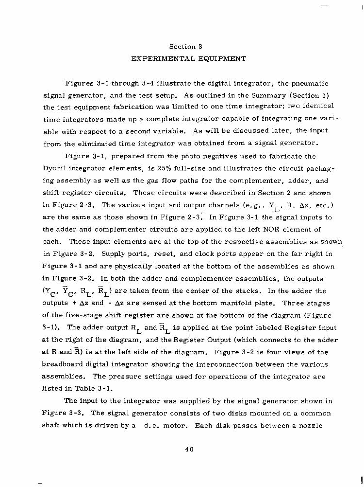
EXPERIMENTAL EQUIPMENT
Figures 3 - 1 through 3-4 illustrate the digital integrator, the pneumatic
signal generator, and the test setup. A s outlined i n the Summary (Section 1) the test equipment fabrication w a s limited to one time integrator; kw0 identical
t ime integrators made up a complete integrator capable of integrating one vari-
able with respect to a second variable. As wi l l be discussed later, the input
from the eliminated t ime integrator w a s obtained from a signal generator.
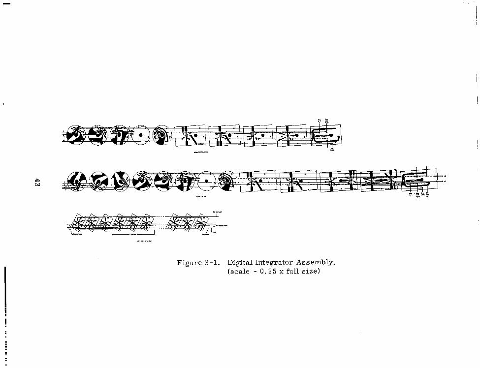
Figure 3-1, prepared from the photo negatives used to fabricate the
Dycril integrator elements, is 25% full-size and illustrates the circuit packag-
ing assembly as well as the gas flow paths for the complementer, adder, and
shift register circuits. These circuits were described in Section 2 and shown
in Figure 2-3 . The various input and output channels (e. g., YL, R, Ax, etc . )
a r e t he s ame as those shown in Figure 2-3. In F igure 3-1 the signal inputs to
the adder and complementer circuits are applied to the left NOR element of
Each. These input elements are at the top of the respective assemblies as shown
in Figure 3-2 . Supply ports, reset , and clock ports appear on the far r ight in
Figure 3-1 and a r e physically located at the bottom of the assemblies as shown
in Figure 3-2 . In both the adder and complementer assemblies, the outputs - (Yc, Yc, RL, R ) are taken f rom the center of the stacks. In the adder the
- L
outputs + Az and - Az are sensed at the bottom manifold plate. Three stages
of the five-stage shift register are shown at the bottom of the diagram (Figure
3-1 ) . The adder output RL and E is applied at the point labeled Register Input
at the right of the diagram, and theRegister Output (which connects to the adder
at R and E) is at the left side of the diagram. Figure 3-2 is four views of the
breadboard digital integrator showing the interconnection between the various
assemblies. The pressure sett ings used for operations of the in tegra tor a re
listed in Table 3-1 .
L
The input to the integrator was supplied by the signal generator shown in
Figure 3-3 . The signal generator consists of two disks mounted on a common
shaft which is driven by a d. c. motor. Each disk passes between a nozzle
4 0
I
and receiver; thus a pressure signal is generated when a slot on the disk un-
covers a receiver. The top disk was employed to generate the integrator input,
YL, and its inversion, y Any 5-bit binary number can be used for Y by
proper arrangement of the open slots on the disk. The bottom disk provided
the clock, read, and reset signals necessary for integrator operation. Mount-
ing of the two disks on a single shaft insured exact synchronization of the input
and clock, read, and reset signals. The proper". c. level for the clock pres-
s u r e w a s established by using an aspirator mounted on the generator.
L' L
1 1
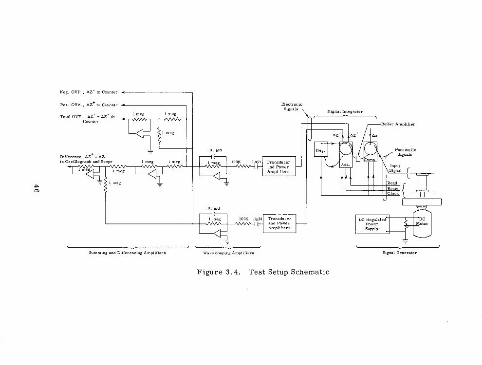
Figure 3-4 summarizes the salient features of the experimental test
setup. The digital integrator and signal generator previously described are
shown in the right portion of the Figure. The various summing, differencing,
and filtering operations shown in the left portion of the Figure were accom-
plished with a small electronic analog computer to conveniently supply test
signals. The waveshaping amplifiers were employed to remove d. c. compo-
nents from the overflow signals (+ Az and - A z ) from the transducer amplifiers
prior to applying these signals to the summing and differencing amplifiers and
then to an electronic counter. Both negative, positive, and total overflow could
be counted. Since an overflow is produced every iteration, the signal generator
frequency could be quite accurately set by counting the total overflow against a
known time base. Overflow difference w a s available at the left-hand amplifier
for display on an oscillograph and oscilloscope. A s wi l l be subsequently
described in Section 4 , other instrument channels were employed as required
to illustrate various intermediate steps during a computation. Typical wave-
forms are also shown in Section 4.
4 1
I... I- "... .,,.., ,,....,
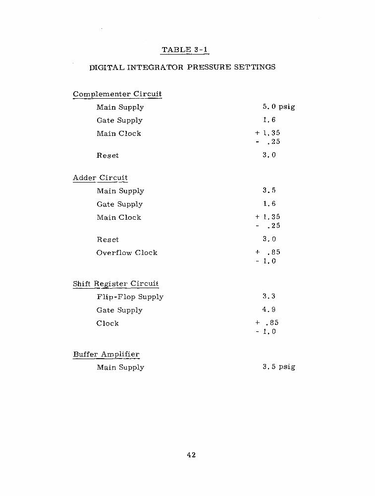
TABLE 3-1
DIGITAL INTEGRATOR PRESSURE SETTINGS
Complementer Ci rcu i t
Main Supply
Gate Supply
Main Clock
Reset
Adder Circui t
Main Supply
Gate Supply
Main Clock
Reset
Overflow Clock
Shift Register Circuit
Flip-Flop Supply
Gate Supply
Clock
Buffer Amplifier
Main Supply
5. 0 psig
1. 6
+ 1.35 - . 2 5
3 .0
3.5
1 .6
+ 1.35 - - 2 5
3 . 0
+ . 8 5 - 1.0
3.3
4 . 9
+ . 85 - 1 . 0
3. 5 psig
42
I
tP W
Figure 3 -1. Digital Integrator Assembly. (scale - 0 . 2 5 x full s i ze )
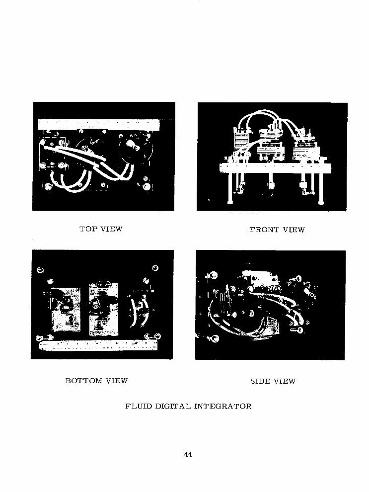
TOP VIEW FRONT VIEW
BOTTOM VIEW SIDE VIEW
FLUID DIGITAL INTEGRATOR
44
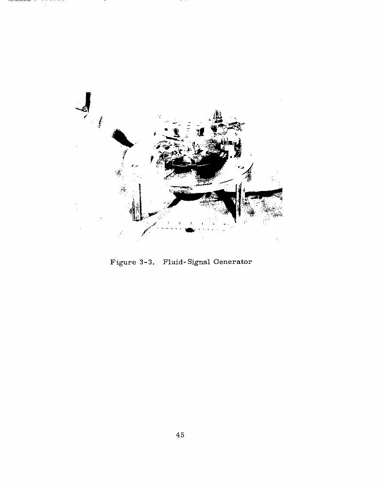
Figure 3 - 3. Fluid- Signal Generator
45
Neg. OVF., AZ- to Counter 4
os. OVF., AZ' to Counter I Total OVF., AZ' + AZ- to
1 meg I rneg
Counter
I, + Difierence. AZ' - AZ-
- I to Oscillograph and Scope
I I a e g
Electronic Signals ,
. 01 pfd I / I \
1 meg
Amplifiers and Power
- - - \ w ) \
Y I
Summing and Difierencing Amplifiers Wave Shaping Amplifiers
Digital Integrator
\ ' -. \ + -Buiier Amplifier
DC Regulated Power
- - -
Signal Generator
Figure 3. 4. Test Setup Schematic
Section 4
EXPERIMENTAL RESULTS
Figures 4 - 3 through 4 - 12 and Table 4 - 1 present typical data taken during
check-out of the integrator. In all tests the clock frequency was maintained at
approximately 100 cycles per second and supply pressures were maintained at
the values listed in Section 3.
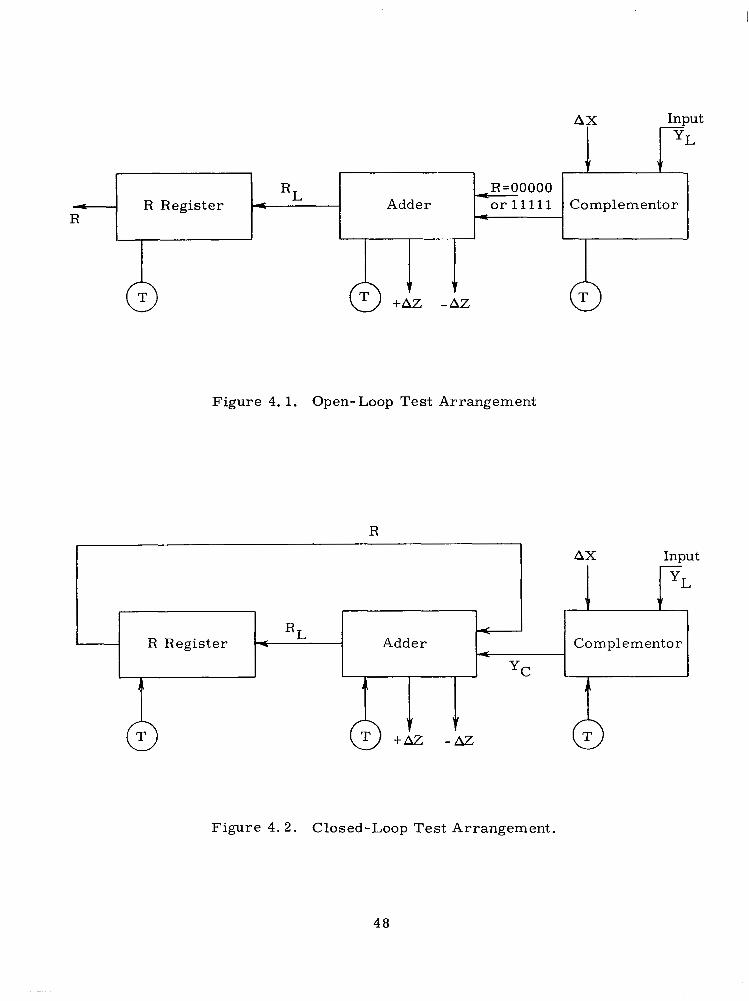
The first four runs were conducted open-loop in that the shift register
output w a s not fed back to the adder as shown in Figure 4-1. In these tests
the signal applied at R was 0 0 0 0 0 o r 1 1 1 1 1 so that the input test signal
(YL), after passing through the complementer, could either be added to or sub-
tracted from these numbers. Thus, the integrator without feedback w a s oper-
ated as an adder or subtractor with the adder output being shifted serially
through the register. These runs served to illustrate some typical wave forms
a s wel l as a check-out of interconnected integrator components. The last 8
runs w e r e conducted in a cloosed-loop configuration with the circuit connected
as shown in Figure 4-2 . The input, YL, was generated by means of a binary-
coded disk as previously described in Section 3 . The value of Y arbitrari ly
w a s chosen to be 1 0 1 0 1 and the results to be presented may be compared
with the computer runs of Table 2- 1. A short description of each run is pre-
sented in the following paragraphs.
L
47
i
A X - Input YL
I Y
RL -R=00000 R Register Complementor or 11 11 1 Adder -
R d -
Figure 4.1. Open-Loop Test Arrangement
R
AX Input - yL
y I /
I R L 4 R Register Complementor Adder
c
yC I ri
Figure 4 .2 . Closed-Loop Test Arrangement.
48

4 +
OVERFLOW A Z t SHIFT REGISTER O U T P U T
ADDER O U T P U T
COMPLE- MENTER OUTPUT
C O M P L E - MENTER INPUT
CLOCK
R
RL
yC
yL
T
T5 T T3 Tg T
Y = 1 0 1 0 1
+ 0 0 0 0 0
4 1
C
R L = 1 0 1 0 1
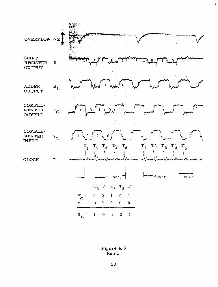
Figure 4. 3 Run 1
50
Run 1 - In this run Y w a s added to R = 00000 (R = 00000 w a s produced L by reducing the pressure at the "R" port to zero). Y L J applied at the comple-
menter input, was passed directly through the complementer since a steady
pressure w a s applied at the Ax port indicating a + Ax. Note that the comple-
menter input, Y L J complementer output, Y c J and adder output, R L J wave-
forms are all s imilar but shifted in phase due to signal delay in the elements
making up these circuits. For convenience in interpreting the data, a space
is'allowed between the fifth pulse of one iteration and the first pulse of the
following iteration (see lower trace Figure 4-3). The shift-register output-
waveform is shifted in phase by one entire iteration since the input signal
appears at the output after 5 clock pulses. Its output waveform is slightly
different from the input since the register retains the last information (in this
case a 1") during the space between iterations. The one iteration delay in
the shift register can be seen in Figure 4-3; at t ime T the adder output (R i s 1 which appears as R = 1 at time T (one iteration later) at the register 1 output. The adder output is 0 which appears at the register output a s a 0 at
t ime T ' and so forth through T and T5'. Thus in this test register output is
the same as the input to the system. Since the sum of 10101 and 00000 do not
produce a carry a t t ime T all negative overflows a r e produced (top channel
of Figure 4-3).
I I
1 L
2 5
5'
51
""11 m.1111111 I 1111 1111. .1.1.11111 11111111
OVERFLOW A Z i SHIFT REGISTER O U T P U T
ADDER OUTPUT
COMPLE- MENTER OUTPUT
COMPLE- MENTER INPUT
CLOCK
R
RL
yC
yL
T
T5 T Tg Tg T 4 1
Y = 1 0 1 0 1
+ 1 1 1 1 1 C
___c
Tim e
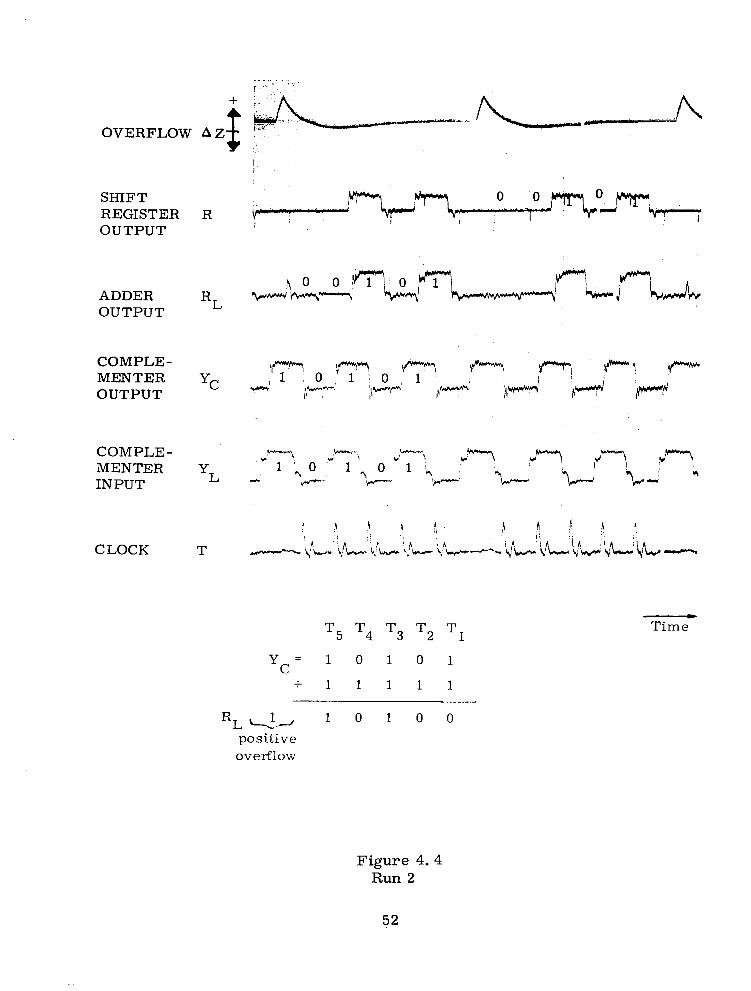
Figure 4.4 Run 2
Run 2 - This run was s imilar to Run 1; the input (Y, =
10101) was passed directly through the complementer (by
maintaining a p res su re at Ax to provide a +Ax) to the adder
where it was summed with 11 111 (steady pressure held at
port R ) producing the sum, 10100, at the adder output. This
number again w a s shifted through the register to provide the
output. A s shown in Figure 4 -4, the addition of the two num-
bers produces a sum larger than 5 bits; thus, a positive
overflow is generated at the upper channel of F igure 4-4.
53
SHIFT REGISTER O U T P U T
ADDER O U T P U T
COMPLE- MENTER O U T P U T
C O M P L E - MENTER INPUT
CLOCK
"
Time
yC = 0 1 0 1 1
+ 0 0 0 0 0
R = 0 1 0 1 1 I ,
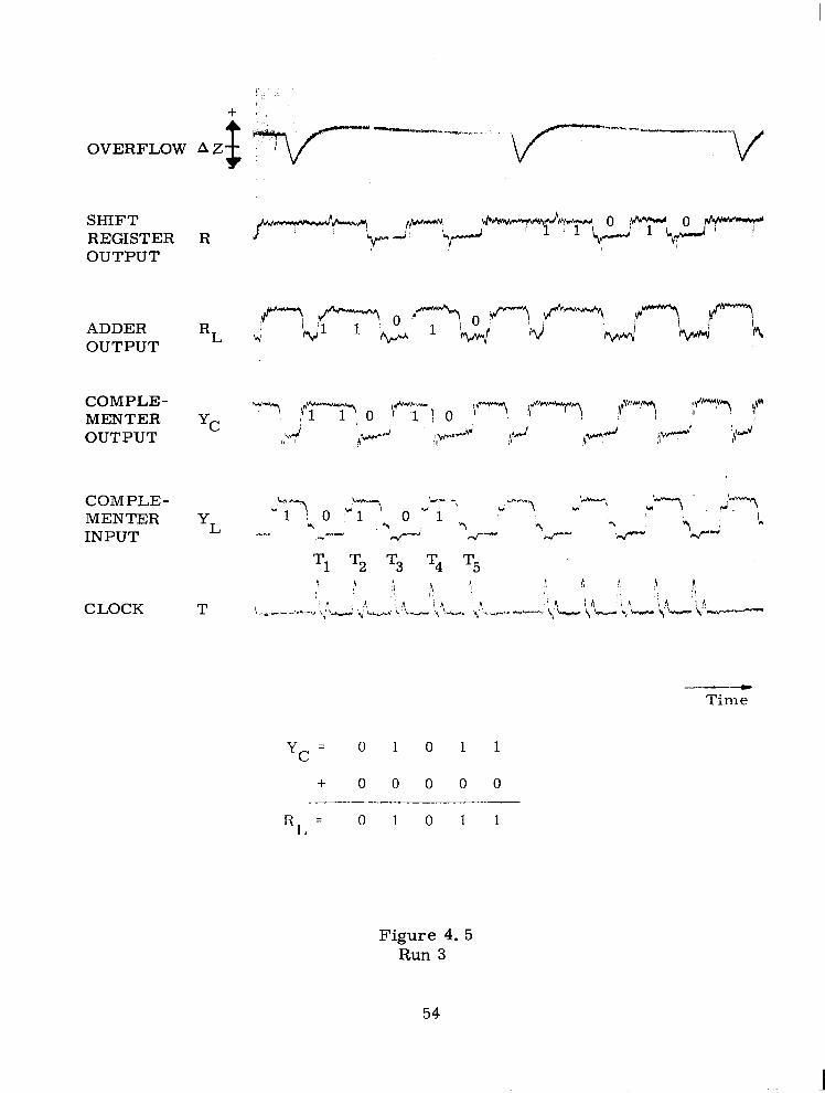
Figure 4. 5 Run 3
54
Run 3 - In this run as wel l as Run 4, the open-loop integra-
t o r was operated simply as a subtractor. An input of 00000 w a s
applied at R (zero pressure at port I'R"),and the input Y = 10101
was complemented in passing through the complementer to pro-
duce Y = 01011 which was then fed to the adder. The results
are shown in Figure 4 - 5 .
L
C
The waveforms shown illustrate the subtraction of +5 from
-16 to yield the correct result of -21, +5 is represented by the
input, YL = lOlOl* and -16 is represented by R = 00000. The
number -21 is displayed at the adder output, RL, as R L = 11010
= -5 and one negative overflow which represents the correct
value - 2 1 (-5 -16). As shown on the top channel of Figure 4 - 5
and also as indicated in the arithmetic shown in the Figure, no
ca r ry w a s generated after the last digits were added correspond-
ing to negative overflow.
Each binary number must be biased by -16 units as stated in Section 2 - 3.
55
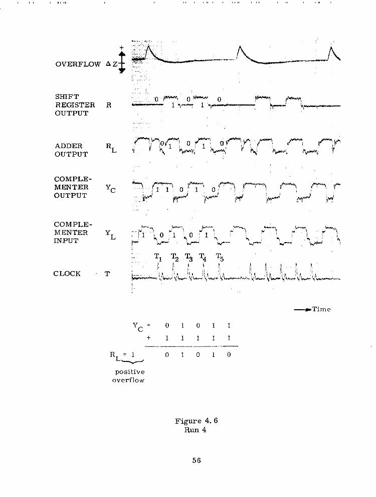
OVERFLOW
SHIFT REGISTER O U T P U T
ADDER O U T P U T
COMPLE- MENTER OUTPUT
C O M P L E - MENTER INPUT
CLOCK :
R
RL
yC
yL
T
. . .
. . .
, . . . . . . .- *1 T2 T3 T4 T5
"Time
Y c = 0 1 0 1 1
+ 1 1 1 1 1
R = 1 0 1 0 1 0 L. positive
overflow
Figure 4.6 Run 4
5 6
Run 4 - In this run the input 10101 was subtracted from
11 111 by complementing the input before applying it to the
adder. All positive overflows as well as the cor rec t sum a re
produced at the adder output and then clocked forward into the
register.
57
ADDER OUTPUT RL
C O M P L E - MENTER I N P U T
CLOCK
yL
T
T T2 T 'T T5 1 3 4
Time -
R L = 1 1 1 0 1
+ 0 0 0 0 0
1 1 1 0 1
Figure 4 . 7 Run 5
58

Run 5 - This run as wel l as all succeeding runs w a s con-
ducted closed-loop. The shift register output was connected
back to the adder input as shown in Figure 4 - 2 to result in the
complete circuit. If a number is placed in the register and the
integrator input , YL, is reduced to zero, this is equivalent to
adding zero to the register contents, producing the sum at the
adder output, and clocking this sum back into the register.
Thus, the same number continues to circulate through the
integrator at clock frequency. Figure 4-7 , Run 5, presents
results obtained in a tes t of this type. Since no ca r ry is pro-
duced after T," all negative overflows are generated as shown
by the top oscillograph channel.
59
"" """"_."-.-""-."-
OVERFLOW A Z i SHIFT REGISTER OUTPUT
ADDER OUTPUT
COMPLE- MENTER OUTPUT
COMPLE- MENTER INPUT
CLOCK
R
RL
yC
yL
T
-.-
Time
Figure 4.8 Run 6
60
- This Run (Figure 4-8) was similar to Run 5 except
that a different number w a s inserted in the register and the test
w a s car r ied out for a longer period of time. The data of both
Runs 5 and 6 illustrate the memory retention of the integrator.
The remainder of the runs presented show data obtained w h i l e operating
the circuit as an integrator and connected as shown in Figure 4 - 2 . Inputs of
Y andAx a r e applied to the complementer. In all cases Y w a s the binary
number 10101 generated by the pneumatic signal generator running in syn-
chronization with clock frequency. Thus, the signal generator replaced the
output of the upper "Y" regis ter of F igure 2-2 and supplied the constant number
= 10101. If a pressure is applied at A x (corresponds to +Ax), Y L is passed
I, L
yL directly through the complementer and a positive ramp output should be obtained
as expected from the time integration of a constant. If Ax is absent (corres-
ponds to - Ax), Y is complemented before being sent to the adder and a nega-
tive ramp output of the same slope should be obtained. The ramp outputs are
represented by the algebraic accumulation of the +Az and -Az pulses as shown
by NET OVERFLOW column in Figure 2-1. The input binary number 10101
produces 1.9 positive Az overflows for each negative overflow (see O V E R F L O W
RATIO column, Figure 2 - 1). An input binary number of 0 101 1 (complement of
10101) should produce 0.526 positive overflows (reciprocal of 1.9) for each
negative overflow.
L
62
OVERFLOW
SHIFT REGISTER OUTPUT
ADDER OUTPUT
COMPLE- MENTER OUTPUT
COMPLE- MENTER INPUT
CLOCK
R
R L
yC
yL
T
T T, T3 T2 T 5 4 1
1 0 1 0 1 Comp. Input
Comp. Output Yc 1 0 1 0 1 (Since AX = 1) yL
+ Register Output R + l o o 0 1 I terat ion
Adder Output = RL 1 0 0 1 1 0 (This number fed into shift register to become register output for succeeding i teration)
+ -2 +A Z
" Comp. Output
i yC 1 0 1 0 1
Second + Register Output R I terat ion + 0 0 1 1 0 (Also adder output from last i teration)
. Adder Output R 1 1 0 1 1 (No carry developed @ T5; There- L\
- +hz fo re - A Z )
- i Comp. Output *C 1 0 1 0 1
I terat ion Third ' + Register Output R + I 1 0 1 1 -
Time
Adder Output R 1 1 0 0 0 0
+Az L. "2
Figure 4. 9 Run 7
62
Run 7 - Figure 4 - 9 presents three i terations by the inte-
grator and the ari thmetic processes are shown below the trace.
In this test Y was not complemented, and the integration thus
represented the function z =)+5) dt. L
63
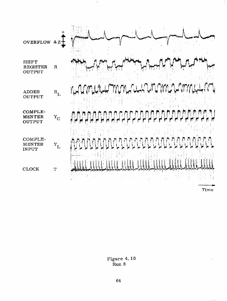
. ..
C O M P L E - MENTER INPUT yL
T CLOCK
- Tim e
Figure 4.10 Run 8
64
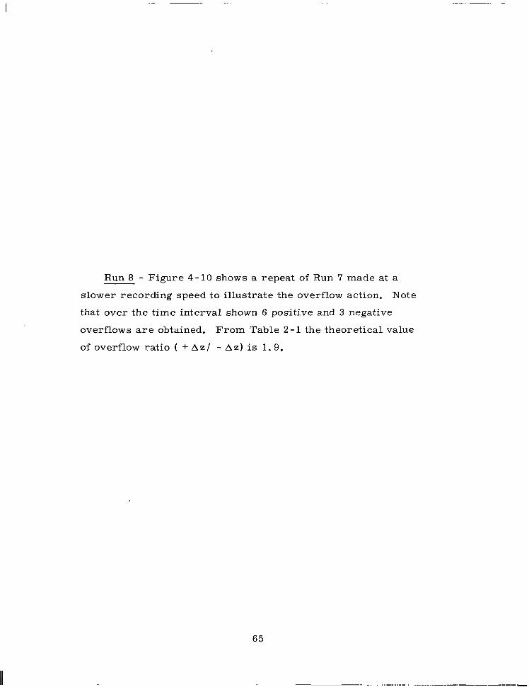
Run 8 - Figure 4-10 shows a repeat of Run 7 made at a
slower recording speed to illustrate the overflow action. Note
that over the time interval shown 6 positive and 3 negative
overflows a r e obtained. From Table 2 - 1 the theoretical value
of overflow ratio ( + Az/ - A z ) is 1. 9.
65
~~ "" _ . . . ".".""."."
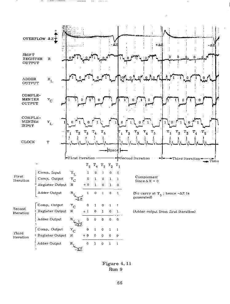
OVERFLOW A 2 i SHIFT REGISTER OUTPUT
ADDER OUTPUT
COMPLE- MENTER OUTPUT
COMPLE- MENTER INPUT
CLOCK
-
R
R L
yC
yL
T
F i r s t I t e r a t ion --
T T4 T3 T2 T 5 1
I Comp. Input yL
*C
1 0 1 0 1
Comp. Output 0 1 0 1 1
Register Output R + 0 1 0 1 0
First Complement I te ra t ion 1 Since A X = 0
I LAdder Output 1 0 1 0 1 (No c a r r y at T5 ; hence -AZ is
-A 2 generated)
r c o m p . o u t p u t yC 0 1 0 1 1 Second Iteration + Register Output R + l o 1 0 1 (Adder output from first iteration)
I Adder Output 0 0 0 0 0
[Camp. Output Y, 0 1 0 1 1 R%
I
Third + Register Output R I te ra t ion , + o o o o o
L
i I Adder Output R L 0 1 0 1 1 L
Figure 4.1 1 Run 9
6 6
Run 9 - F i g u r e 4 - 1 1 is an osci l lograph record and detai led
ari thmetic computation for performing (-5) dt; 3 i terat ions
a r e shown. To obtain the number -5 for integration Y (10101 =
+5) is f i rs t complemented before passing to the adder; o ther-
wise, the comments of Run 8 apply for this run.
J L
67
OVERFLOW A Z i SHIFT REGISTER O U T P U T
ADDER O U T P U T
C O M P L E - MENTER O U T P U T
C O M P L E - MENTER INPUT
CLOCK
R
RL
yC
yL
T
" ~ .. I I
I .
!
d Tim c
Figure 4.12 Run 10
68
Run 10 - Figure 4-12 shows a repeat of Run 9 except that
the data are taken at a lower recording speed to illustrate the
overflow action. A s expected approximately 2 negative over-
flows are obtained for each positive overflow.
69
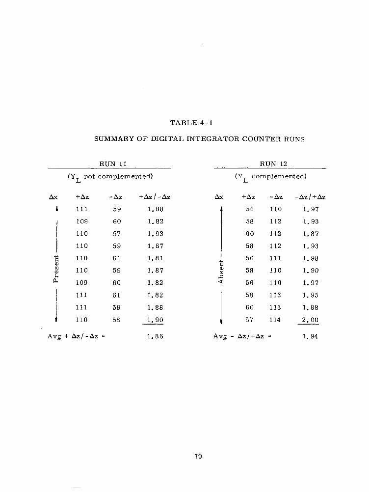
T A B L E 4 - 1
SUMMARY OF DIGITAL INTEGRATOR COUNTER RUNS
RUN 11
(YL not complemented)
A x + Az -Az +Az/-Az
A 111 59 1.88
109 60 1.82 I 110 57 1.93
I llo 59 1.87 + E Q, Lo 110 59 1.87
110 6 1 1.81
k
109 60 1.82
111 6 1 1.82
111 59 1.88
110 58 1.90
RUN 13 - (YL complemented)
Ax +Az -A2 -Az/+Az
A 56 110 1.97
58 112 1.93
60 112 1.87
58 112 1.93 I
c 0,
+ 56 111 1. 98
ro 58 110 1.90
1.97
58 113 1.95
60 113 1.88
57 114 2.00
2 56 110
I A v g - Az/+Az = 1.94
70
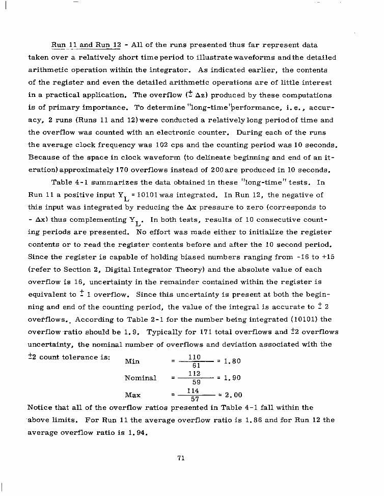
Run 11 and Run 12 - All of the runs presented thus far represent data
taken over a relatively short time period to illustrate waveforms andthe detailed
arithmetic operation within the integrator. As indicated earlier, the contents
of the register and even the detailed arithmetic operations are of little interest
in a practical application. The overflow (2 Az) produced by these computations
is of pr imary importance. To determine "long-time'berformance, i. e. , accur-
acy, 2 runs (Runs 11 and 12) were conducted a relativelylong periodof time and
the overflow was counted with an electronic counter. During each of the runs
the average clock frequency was 102 cps and the counting period w a s 10 seconds.
Because of the space in clock waveform (to delineate beginning and end of an it-
eration) approximately 170 overflows instead of 200 a r e produced in 10 seconds.
Table 4-1 summarizes the data obtained in these "long-time" tests. In
Run 11 a positive input Y = 10101 was integrated. In Run 12 , the negative of
this input was integrated by reducing the Ax pressure to zero (corresponds to
- Ax) thus complementing YL. In both tests, results of 10 consecutive count-
ing periods are presented. No effort was made either to initialize the register
contents or to read the register contents before and after the 10 second period.
Since the register is capable of holding biased numbers ranging from -16 to +15
(refer to Section 2, Digital Integrator Theory) and the absolute value of each
overflow is 16, uncertainty in the remainder contained within the register is
equivalent to 2 1 overflow. Since this uncertainty is present at both the begin-
ning and end of the counting period, the value of the integral is accurate to ? 2
overflows.. According to Table 2-1 for the number being integrated (10101) the
overflow .ratio should be 1.9. Typically for 1 7 1 total overflows and 22 overflows
uncertainty, the nominal number of overflows and deviation associated with the
22 count tolerance is:
L
Min 61
Nominal = 112 = 1.90 59
Max - 114 57 = 2.00
- - 'lo = 1.80
- Notice that all of the overflow ratios presented in Table 4 -1 fall within the
.above limits. For Run 11 the average overflow ratio is 1.86 and for Run 12 the
average overflow ratio is 1.94.
71
Section 5
CONCLUSIONS AND RECOMMENDATIONS
The results and information obtained in the course of this program are
convincing that fluid digital computation systems are feasible. The use of
fluid amplifiers appears attractive for many systems because of high tolerance
to hostile environments such as vibration, radiation and temperature, and
expected reliability. There are inherent disadvantages, however, in the appli-
cation of these fluid devices to digital computation for space systems. The
speed of the fluid amplifier is several orders of magnitude slower than elec-
tronic elements, and some form of a fluid power supply wi l l be needed. There-
fore, fluid amplifiers are not likely to replace most present electronic digital
computation systems, but many specialized applications can use fluid ampli-
fiers advantageously. In these latter applications fluid amplifier implementa-
tion should not be simply a one-for-one replacement of the electronic elements.
In order to be used advantageously the fluid amplifier components must be de-
signed to perform the required functions in the way most suited to their inherent
characteristics. Fo r example, due to the higher speed of electronic devices,
the optimum electronic system may u s e serial implementation with t ime shar-
ing of a single digital integrator while with fluid amplifiers the optimum system
design may be parallel implementation with the use of several digital integra-
tors. Even i f there is no special need for reliability and environmental toler-
ance, the availability of a power source may be a major factor in determining
that fluid amplifier computation should be used. For example, in vehicles
such as boosters, large quantities of pressurized fluid are available and fluid
amplifier computation could be used to eliminate the need for one electrical
source. For long-life satellites no convenient source of fluid power is avail-
able although concepts for solar-powered fluid power sources have been ad-
vanced. Development of these power supplies wil l proceed only when the need
for fluid amplifier computation in satellites becomes more acute.
The major technical accomplishments required in the digital integrator
to achieve prototype performance are to increase speed and to reduce size and
'I 2
and power consumption. Size reduction is especially important since it not
only improves element packing density but also reduces power consumption
and improves element operating speed. The elements used on this project
have nozzles 0.040" x 0.040". It appears quite practical to reduce the element
nozzle size to 0. 010" x 0. 010". Even smaller sizes are possible but do not
appear practical from the contamination and cost considerations. Power con-
sumption can also be reduced by operating at lower pressures; a 0.010'' x
0.010" nozzle operating with 0.1 psig air represents only 2 milliwatts power
consumption. The minimum operating pressures selected w i l l require a com-
promise between speed and power consumption, however, since lowering supply
pressure also decreases operating speed. I t now appears that the optimum
wi l l exist in the 0. 1 to 1. 0 psig range.
Another problem related to smaller size elements is the difficulty of
obtaining sufficiently reliable miniaturized instrumentation for test and moni-
toring purposes. Volumes required for introduction of pressure transducers
represent capitances that can impair response; introduction of probes for flow
measurements may restrict a channel or ser iously alter circuit operation.
The need for some form of f luid buffer to the monitoring equipment appears
likely. The limitation of size reduction to the 0. 010" nozzle wi l l probably be
a practical consideration for the near future applications because of the instru-
mentation problem even i f t he re a r e no other restraints.
Operation of the DI with clock speeds of 1 kc to 5 kc appears practical
using 0.010" nozzle elements. Analog fluid circuits using elements with 0 .016"
x 0.016" nozzles a re operating at speeds over 4 kc. A system operating at
this speed must be carefully designed, however, with concentrated attention
not only to the element design but also to the interconnection techniques. A
DI with a 5 kc clock speed capability wi l l require careful package design to
achieve the optimum layout from internal fluid dynamics considerations as well
as requiring a practical configuration for interconnecting with other DI's.
As can be seen in the data of Appendix A, there is a significant amount
of ''noise" present in the output of fluid amplifiers. While it is difficult to
73
make a numerical evaluation of the seriousness of this noise without consider-
ing a specific application, there is little doubt that signal/noise characteristics
of fluid elements are going to be a problem area in future applications. The
digital computation systems should enjoy an advantage over the analog systems
in this area since they are basically ON-OFF in nature while the analog systems
a r e amplitude sensitive. The equipment developed for this project did not en-
counter any difficulty due to noise.
Summarizing these comments, there are five areas requiring additional
effort for further development of the digital integrator. It is recommended that
continued work be undertaken within the framework of a specific application to
provide realistic and useful specifications and to identify some of the system
interface problems. These five areas are:
1. miniaturization
2. higher speed
3. lower supply pressures
4. integrated design
5. instrumentation.
74
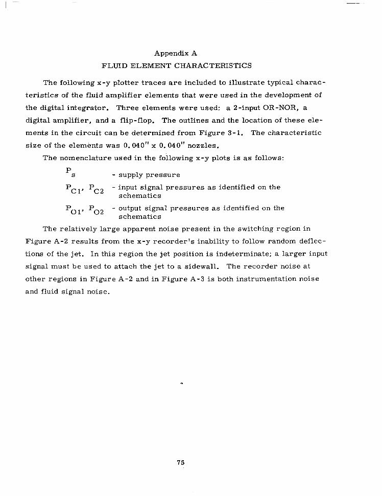
Appendix A
FLUID ELEMENT CHARACTERISTICS
The following x-y plotter traces are included to illustrate typical charac-
ter is t ics of the fluid amplifier elements that were used in the development of
the digital integrator. Three elements were used: a 2-input OR-NOR, a
digital amplifier, and a flip-flop. The outlines and the location of these ele-
ments in the circuit can be determined from Figure 3 - 1 . The characteristic
s ize of the elements w a s 0.040'' x 0.040" nozzles.
The nomenclature used in the following x-y plots is a s follows:
P
Pcl, Pc2 - input signal pressures as identified on the
S - supply pressure
schematics
p 0 2 - output signal pressures as identified on the schematics
The relatively large apparent noise present in the switching region in
Figure A-2 results from the x-y recorder's inability to follow random deflec-
tions of the jet. In this region the jet position is indeterminate; a larger input
signal must be used to attach the jet to a sidewall. The recorder noise at
other regions in Figure A-2 and in Figure A-3 is both instrumentation noise
and fluid signal noise.
75
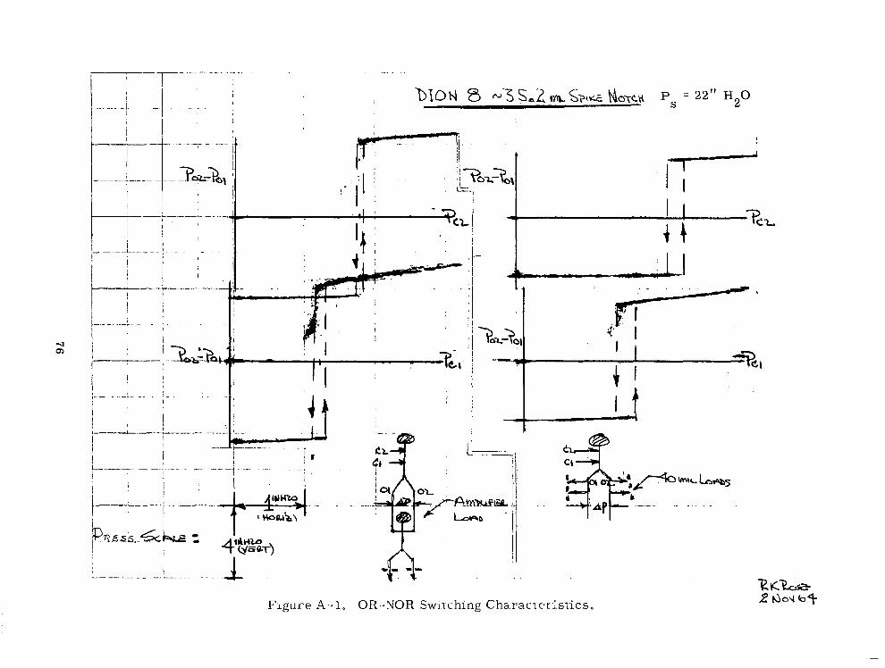
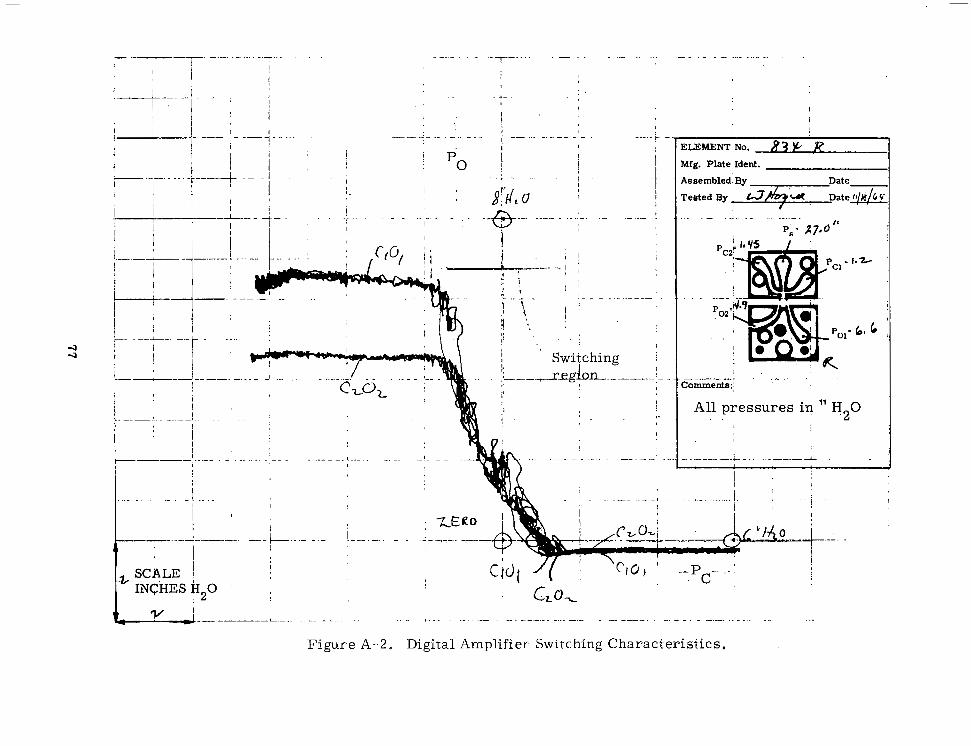
4 4
t Y -i _. - ~ ... _ _ _ - _ . __ . I . .. - .... . ..
Figure A-2. Digital Amplifier: Switching Characteristics.
Figure A-3. Flip-Flop Switching Characteristics.
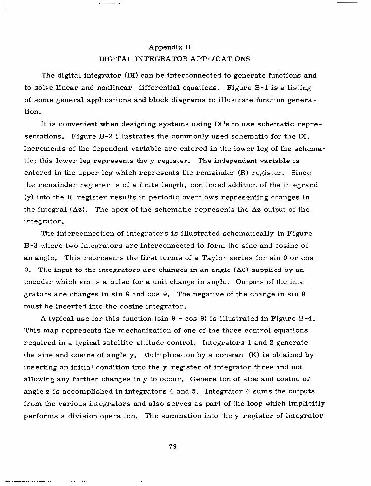
Appendix B
DIGITAL INTEGRATOR APPLICATIONS
The digital integrator (DI) can be interconnected to generate functions and
to solve linear and nonlinear differential equations. Figure B- 1 is a listing
of some general applications and block diagrams to illustrate function genera-
tion.
It is convenient when designing systems using DI's to use schematic repre-
sentations. Figure B-2 illustrates the commonly used schematic for the DI.
Increments of the dependent variable are entered in the lower leg of the schema-
tic; this lower leg represents the y register. The independent variable is
entered in the upper leg which represents the remainder (R) register. Since
the remainder register is of a finite length, continued addition of the integrand
(y) into the R register results in periodic overflows representing changes i n
the integral ( A z ) . The apex of the schematic represents the Az output of the
integrator.
The interconnection of integrators is illustrated schematically in Figure
B-3 where two integrators are interconnected to form the sine and cosine of
an angle. This represents the f irst terms of a Taylor ser ies for s in 8 or cos
8. The input to the integrators are changes in an angle (A@) supplied by an
encoder which emits a pulse for a unit change in angle. Outputs of the inte-
grators are changes in s in 8 and cos 8. The negative of the change in sin 8
must be inserted into the cosine integrator.
A typical use for this function (sin 8 - cos 8) is illustrated in Figure B-4.
This map represents the mechanization of one of the three control equations
required in a typical satellite attitude control. Integrators 1 and 2 generate
the sine and cosine of angle y. Multiplication by a constant (K) is obtained by
inserting an initial condition into the y reg is te r of integrator three and not
allowing any further changes in y to occur. Generation of sine and cosine of
angle z is accomplished in integrators 4 and 5. Integrator 6 sums the outputs
from the various integrators and also serves as part of the loop which implicitly
performs a division operation. The summation into the y regis ter of integrator
79

6 is accomplished by either accumulating the increments by a counter o r add-
ing them in sequence (through the adder) into the y register. The output of
integrator 6 represents the change of the desired control angle (Az) .
80
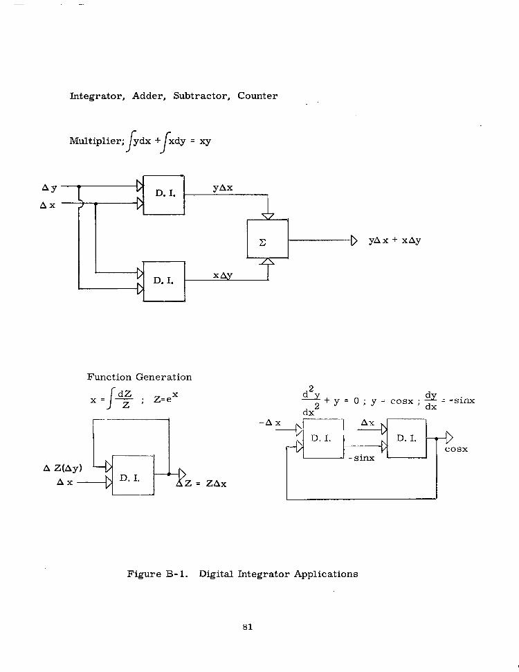
Integrator, Adder, Subtractor, Counter
Multiplier; ydx + xdy = xy J J A Y YAX A x
z [> yAx + xAy
4 X U c
Function Generation
x =IT d Z ; Z = e X
-A
Figure B- 1. Digital Integrator Applications
81
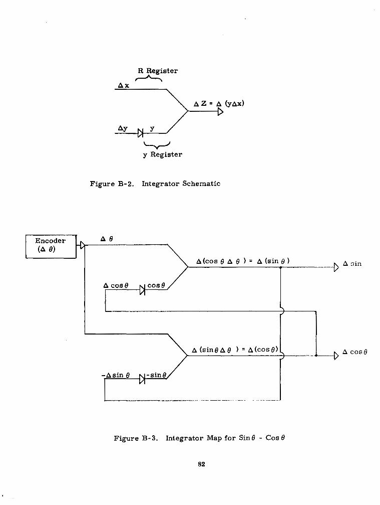
Encoder
+ R Register
+/ y Register
Figure B-2. Integrator Schematic
A 8
\ A k o s 8 A e = A (si: /
A cos 8 Y
Figure B-3. Integrator Map for Sin 8 - Cos 8
82
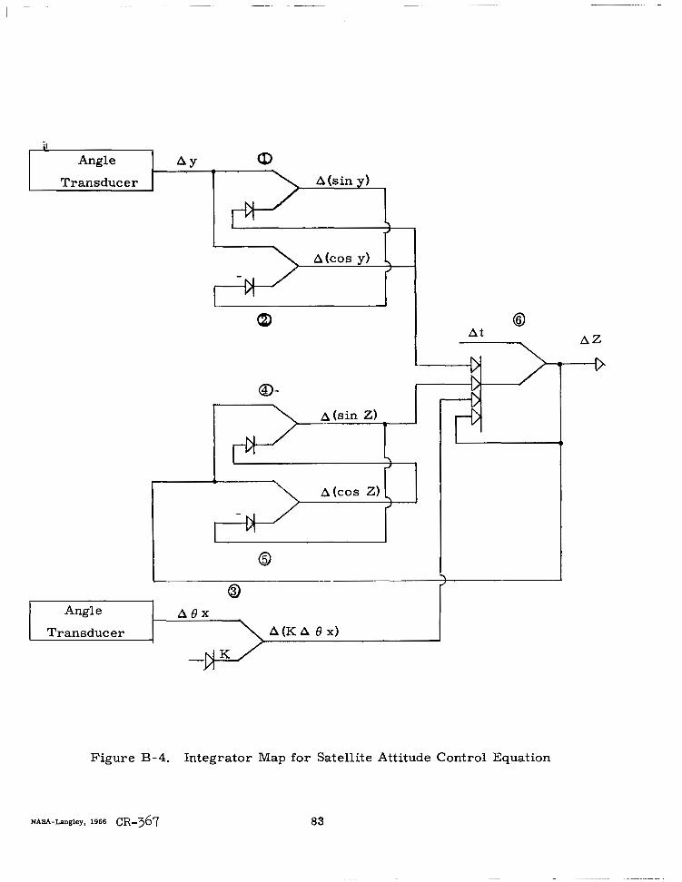
Angle AOx
Transducer
Figure B-4. Integrator Map for Satellite Attitude Control Equation
83