
lm2595-d.pdf - onsemi
26
To learn more about onsemi™, please visit our website at www.onsemi.com ON Semiconductor Is Now onsemi and and other names, marks, and brands are registered and/or common law trademarks of Semiconductor Components Industries, LLC dba “onsemi ” or its affiliates and/or subsidiaries in the United States and/or other countries. onsemi owns the rights to a number of patents, trademarks, copyrights, trade secrets, and other intellectual property. A listing of onsemi product/patent coverage may be accessed at www.onsemi.com/site/pdf/Patent-Marking.pdf. onsemi reserves the right to make changes at any time to any products or information herein, without notice. The information herein is provided “as-is” and onsemi makes no warranty, representation or guarantee regarding the accuracy of the information, product features, availability, functionality, or suitability of its products for any particular purpose, nor does onsemi assume any liability arising out of the application or use of any product or circuit, and specifically disclaims any and all liability, including without limitation special, consequential or incidental damages. Buyer is responsible for its products and applications using onsemi products, including compliance with all laws, regulations and safety requirements or standards, regardless of any support or applications information provided by onsemi. “Typical” parameters which may be provided in onsemi data sheets and/ or specifications can and do vary in different applications and actual performance may vary over time. All operating parameters, including “Typicals” must be validated for each customer application by customer’s technical experts. onsemi does not convey any license under any of its intellectual property rights nor the rights of others. onsemi products are not designed, intended, or authorized for use as a critical component in life support systems or any FDA Class 3 medical devices or medical devices with a same or similar classification in a foreign jurisdiction or any devices intended for implantation in the human body. Should Buyer purchase or use onsemi products for any such unintended or unauthorized application, Buyer shall indemnify and hold onsemi and its officers, employees, subsidiaries, affiliates, and distributors harmless against all claims, costs, damages, and expenses, and reasonable attorney fees arising out of, directly or indirectly, any claim of personal injury or death associated with such unintended or unauthorized use, even if such claim alleges that onsemi was negligent regarding the design or manufacture of the part. onsemi is an Equal Opportunity/Affirmative Action Employer. This literature is subject to all applicable copyright laws and is not for resale in any manner. Other names and brands may be claimed as the property of others.
-
Upload
khangminh22 -
Category
Documents
-
view
1 -
download
0
Transcript of lm2595-d.pdf - onsemi

To learn more about onsemi™, please visit our website at www.onsemi.com
ON Semiconductor
Is Now
onsemi and and other names, marks, and brands are registered and/or common law trademarks of Semiconductor Components Industries, LLC dba “onsemi” or its affiliates and/or subsidiaries in the United States and/or other countries. onsemi owns the rights to a number of patents, trademarks, copyrights, trade secrets, and other intellectual property. A listing of onsemi product/patent coverage may be accessed at www.onsemi.com/site/pdf/Patent-Marking.pdf. onsemi reserves the right to make changes at any time to any products or information herein, without notice. The information herein is provided “as-is” and onsemi makes no warranty, representation or guarantee regarding the accuracy of the information, product features, availability, functionality, or suitability of its products for any particular purpose, nor does onsemi assume any liability arising out of the application or use of any product or circuit, and specifically disclaims any and all liability, including without limitation special, consequential or incidental damages. Buyer is responsible for its products and applications using onsemi products, including compliance with all laws, regulations and safety requirements or standards, regardless of any support or applications information provided by onsemi. “Typical” parameters which may be provided in onsemi data sheets and/or specifications can and do vary in different applications and actual performance may vary over time. All operating parameters, including “Typicals” must be validated for each customer application by customer’s technical experts. onsemi does not convey any license under any of its intellectual property rights nor the rights of others. onsemi products are not designed, intended, or authorized for use as a critical component in life support systems or any FDA Class 3 medical devices or medical devices with a same or similar classification in a foreign jurisdiction or any devices intended for implantation in the human body. Should Buyer purchase or use onsemi products for any such unintended or unauthorized application, Buyer shall indemnify and hold onsemi and its officers, employees, subsidiaries, affiliates, and distributors harmless against all claims, costs, damages, and expenses, and reasonable attorney fees arising out of, directly or indirectly, any claim of personal injury or death associated with such unintended or unauthorized use, even if such claim alleges that onsemi was negligent regarding the design or manufacture of the part. onsemi is an Equal Opportunity/Affirmative Action Employer. This literature is subject to all applicable copyright laws and is not for resale in any manner. Other names and brands may be claimed as the property of others.

© Semiconductor Components Industries, LLC, 2009
February, 2009 − Rev. 21 Publication Order Number:
LM2595/D
LM2595
1.0 A, Step-Down SwitchingRegulator
The LM2595 regulator is monolithic integrated circuit ideally suitedfor easy and convenient design of a step−down switching regulator(buck converter). It is capable of driving a 1.0 A load with excellentline and load regulation. This device is available in adjustable outputversion and it is internally compensated to minimize the number ofexternal components to simplify the power supply design.
Since LM2595 converter is a switch−mode power supply, itsefficiency is significantly higher in comparison with popularthree−terminal linear regulators, especially with higher input voltages.
The LM2595 operates at a switching frequency of 150 kHz thusallowing smaller sized filter components than what would be neededwith lower frequency switching regulators. Available in a standard5−lead TO−220 package with several different lead bend options, andD2PAK surface mount package.
The other features include a guaranteed �4% tolerance on outputvoltage within specified input voltages and output load conditions, and�15% on the oscillator frequency. External shutdown is included,featuring 50 �A (typical) standby current. Self protection featuresinclude switch cycle−by−cycle current limit for the output switch, aswell as thermal shutdown for complete protection under faultconditions.
Features• Adjustable Output Voltage Range 1.23 V − 37 V
• Guaranteed 1.0 A Output Load Current
• Wide Input Voltage Range up to 40 V
• 150 kHz Fixed Frequency Internal Oscillator
• TTL Shutdown Capability
• Low Power Standby Mode, typ 50 �A
• Thermal Shutdown and Current Limit Protection
• Internal Loop Compensation
• Moisture Sensitivity Level (MSL) Equals 1
• Pb−Free Packages are Available
Applications• Simple High−Efficiency Step−Down (Buck) Regulator
• Efficient Pre−Regulator for Linear Regulators
• On−Card Switching Regulators
• Positive to Negative Converter (Buck−Boost)
• Negative Step−Up Converters
• Power Supply for Battery Chargers
See detailed ordering and shipping information in the packagedimensions section on page 23 of this data sheet.
ORDERING INFORMATION
1
5
TO−220TV SUFFIXCASE 314B
1
5
Heatsink surface connected to Pin 3
TO−220T SUFFIX
CASE 314D
Pin 1. Output2. Vin3. Ground4. Feedback5. ON/OFF
D2PAKD2T SUFFIXCASE 936A
Heatsink surface (shown as terminal 6 incase outline drawing) is connected to Pin 3
1
5
http://onsemi.com
See general marking information in the device markingsection on page 23 of this data sheet.
DEVICE MARKING INFORMATION

LM2595
http://onsemi.com2
Figure 1. Typical Application
LM2595
12 V UnregulatedDC Input +Vin
Cin220 �F/50 V
D11N5822
Cout220 �F
Feedback
ON/OFFGND
5 V @ 1 ARegulatedOutput
L168 �H R2=3.0K
R1=1K
2
3 5
1
4
Output
Cff
Figure 2. Representative Block Diagram
MAXIMUM RATINGS
Rating Symbol Value Unit
Maximum Supply Voltage Vin 45 V
ON/OFF Pin Input Voltage ON/OFF −0.3 V ≤ V ≤ +Vin V
Output Voltage to Ground (Steady−State) Output −1.0 V
Power Dissipation
Case 314B and 314D (TO−220, 5−Lead) PD Internally Limited W
Thermal Resistance, Junction−to−Ambient R�JA 65 °C/W
Thermal Resistance, Junction−to−Case R�JC 5.0 °C/W
Case 936A (D2PAK) PD Internally Limited W
Thermal Resistance, Junction−to−Ambient R�JA 70 °C/W
Thermal Resistance, Junction−to−Case R�JC 5.0 °C/W
Storage Temperature Range Tstg −65 to +150 °C
Minimum ESD Rating (Human Body Model: C = 100 pF, R = 1.5 k�) − 2.0 kV
Lead Temperature (Soldering, 10 seconds) − 260 °C
Maximum Junction Temperature TJ 150 °C
Stresses exceeding Maximum Ratings may damage the device. Maximum Ratings are stress ratings only. Functional operation above theRecommended Operating Conditions is not implied. Extended exposure to stresses above the Recommended Operating Conditions may affectdevice reliability.

LM2595
http://onsemi.com3
PIN FUNCTION DESCRIPTION
Pin Symbol Description (Refer to Figure 1)
1 Output This is the emitter of the internal switch. The saturation voltage Vsat of this output switch is typically 1.0 V. It should bekept in mind that the PCB area connected to this pin should be kept to a minimum in order to minimize coupling tosensitive circuitry.
2 Vin This pin is the positive input supply for the LM2595 step−down switching regulator. In order to minimize voltage transi-ents and to supply the switching currents needed by the regulator, a suitable input bypass capacitor must be present(Cin in Figure 1).
3 GND Circuit ground pin. See the information about the printed circuit board layout.
4 Feedback This pin is the direct input of the error amplifier and the resistor network R2, R1 is connected externally to allow pro-gramming of the output voltage.
5 ON/OFF It allows the switching regulator circuit to be shut down using logic level signals, thus dropping the total input supplycurrent to approximately 50 �A. The threshold voltage is typically 1.6 V. Applying a voltage above this value (up to+Vin) shuts the regulator off. If the voltage applied to this pin is lower than 1.6 V or if this pin is left open, the regulatorwill be in the “on” condition.
OPERATING RATINGS (Operating Ratings indicate conditions for which the device is intended to be functional, but do not guaranteespecific performance limits. For guaranteed specifications and test conditions, see the Electrical Characteristics.)
Rating Symbol Value Unit
Operating Junction Temperature Range TJ −40 to +125 °C
Supply Voltage Vin 4.5 to 40 V

LM2595
http://onsemi.com4
SYSTEM PARAMETERSELECTRICAL CHARACTERISTICS Specifications with standard type face are for TJ = 25°C, and those with boldface type applyover full Operating Temperature Range −40°C to +125°C
Characteristics Symbol Min Typ Max Unit
LM2595 (Note 1, Test Circuit Figure 16)
Feedback Voltage (Vin = 12 V, ILoad = 0.2 A, Vout = 5.0 V, ) VFB_nom 1.23 V
Feedback Voltage (8.0 V ≤ Vin ≤ 40 V, 0.2 A ≤ ILoad ≤ 1.0 A, Vout = 5.0 V) VFB 1.1931.18
1.2671.28
V
Efficiency (Vin = 12 V, ILoad = 1.0 A, Vout = 5.0 V) � − 81 − %
Characteristics Symbol Min Typ Max Unit
Feedback Bias Current (Vout = 5.0 V) Ib 25 100200
nA
Oscillator Frequency (Note 2) fosc 135120
150 165180
kHz
Saturation Voltage (Iout = 1.0 A, Notes 3 and 4) Vsat 1.0 1.21.3
V
Max Duty Cycle “ON” (Note 4) DC 95 %
Current Limit (Peak Current, Notes 2 and 3) ICL 1.21.15
2.1 2.42.6
A
Output Leakage Current (Notes 5 and 6)Output = 0 VOutput = −1.0 V
IL0.513
2.030
mA
Quiescent Current (Note 5) IQ 5.0 10 mA
Standby Quiescent Current (ON/OFF Pin = 5.0 V (“OFF”))(Note 6)
Istby 50 200250
�A
ON/OFF PIN LOGIC INPUT
Threshold Voltage 1.6 V
Vout = 0 V (Regulator OFF) VIH 2.22.4
V
Vout = Nominal Output Voltage (Regulator ON) VIL 1.00.8
V
ON/OFF Pin Input Current
ON/OFF Pin = 5.0 V (Regulator OFF) IIH − 15 30 �A
ON/OFF Pin = 0 V (regulator ON) IIL − 0.01 5.0 �A
1. External components such as the catch diode, inductor, input and output capacitors can affect switching regulator system performance.When the LM2595 is used as shown in the Figure 16 test circuit, system performance will be as shown in system parameters section.
2. The oscillator frequency reduces to approximately 30 kHz in the event of an output short or an overload which causes the regulated outputvoltage to drop approximately 40% from the nominal output voltage. This self protection feature lowers the average dissipation of the IC bylowering the minimum duty cycle from 5% down to approximately 2%.
3. No diode, inductor or capacitor connected to output (Pin 1) sourcing the current.4. Feedback (Pin 4) removed from output and connected to 0 V.5. Feedback (Pin 4) removed from output and connected to +12 V to force the output transistor “off”.6. Vin = 40 V.

LM2595
http://onsemi.com5
I Q, Q
UIE
SCEN
T C
UR
REN
T (m
A)TYPICAL PERFORMANCE CHARACTERISTICS (Circuit of Figure 16)
V out, O
UTP
UT
VOLT
AGE
CH
ANG
E (%
)
, STA
ND
BY Q
UIE
SCEN
T C
UR
REN
T (
TJ, JUNCTION TEMPERATURE (°C)
TJ, JUNCTION TEMPERATURE (°C)
Vin, INPUT VOLTAGE (V)
INPU
T -
OU
TPU
T D
IFFE
REN
TIAL
(V)
TJ, JUNCTION TEMPERATURE (°C)
Figure 3. Normalized Output Voltage
TJ, JUNCTION TEMPERATURE (°C)
Figure 4. Line Regulation
Figure 5. Dropout Voltage Figure 6. Current Limit
Figure 7. Quiescent Current Figure 8. Standby Quiescent Current
L = 68 �HR_ind = 30 m�
ILoad = 200 mA
ILoad = 1 A
μA)
1.0
0.6
0.2
0
-0.2
-0.4
-1.01251007550250−25−50
-0.8
-0.6
0.4
0.8 Vin = 20 VILoad = 200 mANormalized at TJ = 25°C
I stby
1.4
1.2
1.0
0.8
0.6
0.4
0.2
0
−0.2
−0.4
−0.6
Vin, INPUT VOLTAGE (V)
0 5.0 10 15 20 25 30 35 40
Vout = 5 V
ILoad = 200 mATJ = 25°C
Vou
t, O
UT
PU
T V
OLT
AG
E C
HA
NG
E (
%)
−50 −25 0 25 60 75 100 125
1.5
1.0
0.5
0
ILoad = 200 mA
ILoad = 1.0 A
Vout = 5 VMeasured at GND PinTJ = 25°C
0 5 10 15 20 25 30 35 40
12
11
10
9
8
7
6
5
4−50 −25 0 25 60 75 100 125
160
140
120
100
80
60
40
20
0
Vin = 40 V
Vin = 12 V
VON/OFF = 5.0 V
−0.5 0.0
1.0
2.0
3.0
−50 −30 −10 10 30 50 70 90 110 130
SW
ITC
HIN
G C
UR
RE
NT
LIM
IT (
A) Vin = 12 V

LM2595
http://onsemi.com6
V sat, S
ATU
RAT
ION
VO
LTAG
E (V
)
2.0
2.5
3.0
4.0
I b, FEE
DBA
CK
PIN
CU
RR
ENT
(nA)
, IN
PUT
VOLT
AGE
(V)
TJ, JUNCTION TEMPERATURE (°C)
SWITCH CURRENT (A)
NO
RM
ALIZ
ED F
REQ
UEN
CY
(%)
TJ, JUNCTION TEMPERATURE (°C)
Figure 9. Switch Saturation Voltage Figure 10. Switching Frequency
Figure 11. Minimum Supply Operating Voltage Figure 12. Feedback Pin Current
5.0
4.5
3.5
1.5
1.0
0.5
01251007550250-25-50
TJ, JUNCTION TEMPERATURE (°C)
100
80
60
40
20
0
-20
-40
-60
-80
-1001251007550250-25-50
Vout � 1.23 VILoad = 200 mA
TYPICAL PERFORMANCE CHARACTERISTICS (Circuit of Figure 16)V
in
−9.0
−8.0
−7.0
−6.0
−5.0
−4.0
−3.0
−2.0
−1.0
0.0
1.0
−50 −25 0 25 50 75 100 125
−40°C
25°C
125°C
1.3
1.2
1.1
1.0
0.9
0.8
0.7
0.6
0.5
0.4
0.30 0.2 0.4 0.6 0.8 1.0
VIN, INPUT VOLTAGE (V)
EF
FIC
IEN
CY
(%
)
95
90
85
80
75
700 455 403530252010 15
Figure 13. Efficiency
12 V, 1 A
5 V, 1 A
3.3 V, 1 A

LM2595
http://onsemi.com7
0.6 A
0
0
A
B
C
100 �s/div2 �s/div
Figure 14. Switching Waveforms Figure 15. Load Transient Response
Vout = 5 VA: Output Pin Voltage, 10 V/divB: Switch Current, 0.6 A/divC: Inductor Current, 0.6 A/div, AC−CoupledD: Output Ripple Voltage, 50 mV/div, AC−Coupled
Horizontal Time Base: 2.0 �s/div
10 V
0
1.2 A
0.6 A
100 mVOutput
VoltageChange
0
0.5 A
0.1 A
0
1.2 A
- 100 mV
LoadCurrent
TYPICAL PERFORMANCE CHARACTERISTICS (Circuit of Figure 16)
D
Figure 16. Typical Test Circuit
D11N5822
L168 �H
Output
1
4
Feedback
Cout220 �F
Cin100 �F
LM2595
2
53 ON/OFFGND
Vin
Load
Vout5.0 V/1.0 A
Adjustable Output Voltage Versions
Vout � Vref��1.0 �� R2
R1�
R2 � R1�VoutVref
� 1.0�Where Vref = 1.23 V, R1 between 1.0 k and 5.0 k
R2
R1
8.5 V - 40 VUnregulated
DC Input
CFF

LM2595
http://onsemi.com8
PCB LAYOUT GUIDELINES
As in any switching regulator, the layout of the printedcircuit board is very important. Rapidly switching currentsassociated with wiring inductance, stray capacitance andparasitic inductance of the printed circuit board traces cangenerate voltage transients which can generateelectromagnetic interferences (EMI) and affect the desiredoperation. As indicated in the Figure 16, to minimizeinductance and ground loops, the length of the leadsindicated by heavy lines should be kept as short as possible.
For best results, single−point grounding (as indicated) orground plane construction should be used.
On the other hand, the PCB area connected to the Pin 1(emitter of the internal switch) of the LM2595 should bekept to a minimum in order to minimize coupling to sensitivecircuitry.
Another sensitive part of the circuit is the feedback. It isimportant to keep the sensitive feedback wiring short. Toassure this, physically locate the programming resistors nearto the regulator, when using the adjustable version of theLM2595 regulator.
DESIGN PROCEDUREBuck Converter Basics
The LM2595 is a “Buck” or Step−Down Converter whichis the most elementary forward−mode converter. Its basicschematic can be seen in Figure 17.
The operation of this regulator topology has two distincttime periods. The first one occurs when the series switch ison, the input voltage is connected to the input of the inductor.
The output of the inductor is the output voltage, and therectifier (or catch diode) is reverse biased. During thisperiod, since there is a constant voltage source connectedacross the inductor, the inductor current begins to linearlyramp upwards, as described by the following equation:
IL(on) ��VIN � VOUT
�ton
LDuring this “on” period, energy is stored within the core
material in the form of magnetic flux. If the inductor isproperly designed, there is sufficient energy stored to carrythe requirements of the load during the “off” period.
Figure 17. Basic Buck Converter
DVin RLoad
L
Cout
PowerSwitch
The next period is the “off” period of the power switch.When the power switch turns off, the voltage across theinductor reverses its polarity and is clamped at one diodevoltage drop below ground by the catch diode. The currentnow flows through the catch diode thus maintaining the loadcurrent loop. This removes the stored energy from theinductor. The inductor current during this time is:
IL(off) ��VOUT � VD
�toff
L
This period ends when the power switch is once againturned on. Regulation of the converter is accomplished byvarying the duty cycle of the power switch. It is possible todescribe the duty cycle as follows:
d �tonT
, where T is the period of switching.
For the buck converter with ideal components, the dutycycle can also be described as:
d �VoutVin
Figure 18 shows the buck converter, idealized waveformsof the catch diode voltage and the inductor current.
PowerSwitch
Figure 18. Buck Converter Idealized Waveforms
PowerSwitch
Off
PowerSwitch
Off
PowerSwitch
On
PowerSwitch
On
Von(SW)
VD(FWD)
Time
Time
ILoad(AV)
Imin
Ipk
Diode DiodePowerSwitch
Dio
de V
olta
geIn
duct
or C
urre
nt

LM2595
http://onsemi.com9
PROCEDURE (ADJUSTABLE OUTPUT VERSION: LM2595)
Procedure Example
Given Parameters:Vout = Regulated Output VoltageVin(max) = Maximum DC Input VoltageILoad(max) = Maximum Load Current
Given Parameters:Vout = 5.0 VVin(max) = 12 VILoad(max) = 1.0 A
1. Programming Output VoltageTo select the right programming resistor R1 and R2 value (seeFigure 1) use the following formula:
Resistor R1 can be between 1.0 k and 5.0 k�. (For best temperature coefficient and stability with time, use 1% metal film resistors).
Vout � Vref�1.0 � R2
R1�
R2 � R1�Vout
Vref
� 1.0�
where Vref = 1.23 V
1. Programming Output Voltage (selecting R1 and R2)Select R1 and R2:
R2 = 3.07 k�, choose a 3.0k metal film resistor.
R2 � R1�VoutVref
� 1.0� � � 5 V
1.23 V� 1.0�
Vout � 1.23�1.0 � R2R1� Select R1 = 1.0 k�
2. Input Capacitor Selection (Cin)To prevent large voltage transients from appearing at the input and for stable operation of the converter, an aluminium or tantalum electrolytic bypass capacitor is needed between the input pin +Vin and ground pin GND This capacitor should be located close to the IC using short leads. This capacitor should have a low ESR (Equivalent Series Resistance) value.
For additional information see input capacitor section in the “Application Information” section of this data sheet.
2. Input Capacitor Selection (Cin)A 220 �F, 50 V aluminium electrolytic capacitor located near
the input and ground pin provides sufficient bypassing.
3. Catch Diode Selection (D1)A. Since the diode maximum peak current exceeds the
regulator maximum load current the catch diode current rating must be at least 1.2 times greater than the maximum load current. For a robust design, the diode should have a current rating equal to the maximum current limit of the LM2595 to be able to withstand a continuous output short.
B. The reverse voltage rating of the diode should be at least 1.25 times the maximum input voltage.
3. Catch Diode Selection (D1)A. For this example, a 1.0 A (for a robust design 3.0 A diode
is recommended) current rating is adequate.
B. For Vin = 12 V use a 20 V 1N5817 (1N5820) Schottkydiode or any suggested fast recovery diode in the Table 2.

LM2595
http://onsemi.com10
PROCEDURE (ADJUSTABLE OUTPUT VERSION: LM2595) (CONTINUED)
Procedure Example
4. Inductor Selection (L1)A. Use the following formula to calculate the inductor Volt x
microsecond [V x �s] constant:
B. Match the calculated E x T value with the corresponding number on the vertical axis of the Inductor Value Selection Guide shown in Figure 19. This E x T constant is a measure of the energy handling capability of an inductor and is dependent upon the type of core, the core area, the number of turns, and the duty cycle.
C. Next step is to identify the inductance region intersected by the E x T value and the maximum load current value on the horizontal axis shown in Figure 19.
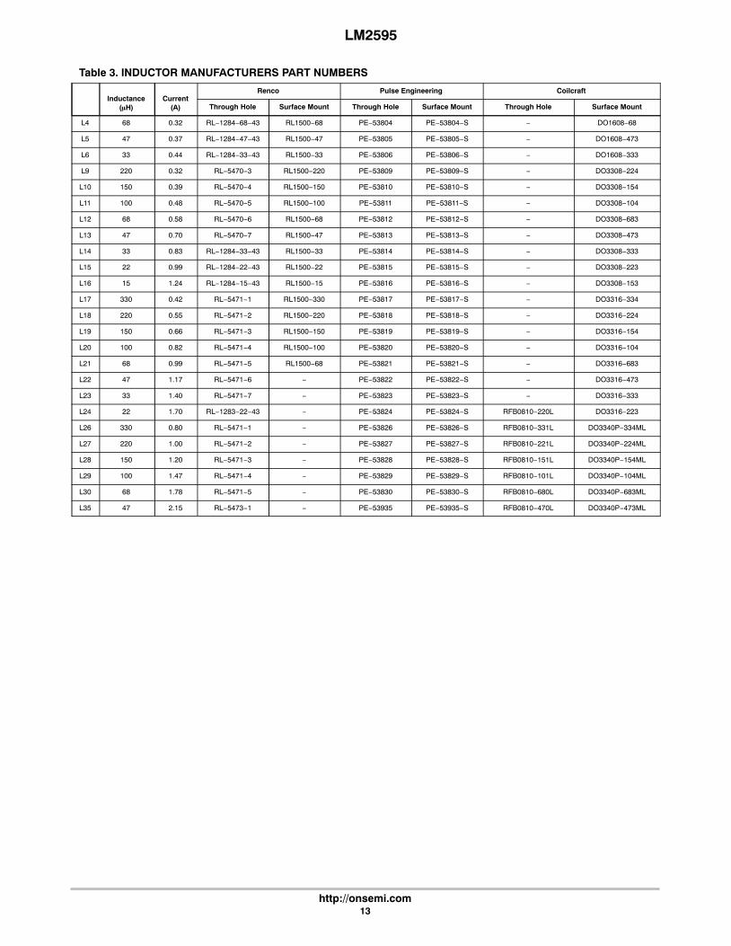
D. Select an appropriate inductor from Table 3. The inductor chosen must be rated for a switching frequency of 150 kHz and for a current rating of 1.15 x ILoad. The inductor current rating can also be determined by calculating the inductor peak current:
where ton is the “on” time of the power switch and
E � T � �VIN � VOUT � VSAT� �
VOUT � VD
VIN � VSAT � VD�
1000
150 kHz�V � �s�
Ip(max) � ILoad(max)��Vin �Vout� ton
2L
ton �VoutVin
x 1.0fosc
4. Inductor Selection (L1)A. Calculate E x T [V x �s] constant:
B. E x T = 19.2 [V x �s]
C. ILoad(max) = 1.0 AInductance Region = L30
D. Proper inductor value = 68 �HChoose the inductor from Table 3.
E � T � �12 � 5 � 1.0� �5 � 0.5
12 � 1 � 0.5�
1000
150 kHz�V � �s�
E � T � �6� �5.5
11.5� 6.7�V � �s�
5. Output Capacitor Selection (Cout)A. Since the LM2595 is a forward−mode switching regulator
with voltage mode control, its open loop has 2−pole−1−zero frequency characteristic. The loop stability is determined by the output capacitor (capacitance, ESR) and inductance values.
For stable operation use recommended values of the output capacitors in Table 1.Low ESR electrolytic capacitors between 180 �F and 1000 �F provide best results.
B. The capacitors voltage rating should be at least 1.5 times greater than the output voltage, and often much higher voltage rating is needed to satisfy low ESR requirement
5. Output Capacitor Selection (Cout)A. In this example, it is recommended to use a Nichicon PM
capacitor: 220 �F/25 V
6. Feedforward Capacitor (CFF)It provides additional loop stability mainly for higher input voltages.For Cff selection use Table 1. The compensation capacitor between0.6 nF and 15 nF is wired in parallel with the output voltage settingresistor R2, The capacitor type can be ceramic, plastic, etc..
6. Feedforward Capacitor (CFF)In this example, it is recommended to use a feedforwardcapacitor 4.7 nF.

LM2595
http://onsemi.com11
LM2595 Series Buck Regulator Design Procedures (continued)
Table 1. RECOMMENDED VALUES OF THE OUTPUT CAPACITOR AND FEEDFORWARD CAPACITOR(Iload = 1.0 A)
Nichicon Pm Capacitors
Vin (V) Capacity/ESR/Voltage Range (�F/m�/V)
40 1000/60/10 1000/60/10 1000/60/10 470/120/10 220/110/25 180/290/25 180/290/25 82/190/35 82/190/35
35 1000/60/10 1000/60/10 1000/60/10 220/110/25 180/140/25 120/200/25 120/200/25 82/190/35 82/190/35
26 1000/60/10 470/120/10 220/110/25 220/110/25 180/140/25 120/200/25 120/200/25 82/190/35
20 1000/60/10 470/120/10 220/110/25 220/110/25 180/140/25 120/200/25 120/200/25
18 1000/60/10 470/120/10 220/110/25 220/110/25 180/140/25 120/200/25 120/200/25
12 470/120/10 470/120/10 220/110/25 220/110/25 180/140/25
10 470/120/10 470/120/10 220/110/25 220/110/25
Vout 2 3 4 6 9 12 15 24 28
Cff (nF) 10 4.7 4.7 4.7 1.5 1.5 1 0.6 0.6
Figure 19. Inductor Value Selection Guides (For Continuous Mode Operation)
E*T
(V*u
s)
MAXIMUM LOAD CURRENT (A)

LM2595
http://onsemi.com12
Table 2. DIODE SELECTION
VR
1A Diodes 3A Diodes
Surface Mount Through Hole Surface Mount Through Hole
SchottkyUltra FastRecovery Schottky
Ultra FastRecovery Schottky
Ultra FastRecovery Schottky
Ultra FastRecovery
20V SK12
All of thesediodes arerated to atleast 50 VMURS120
10BF10
1N5817
All of thesediodes arerated to atleast 50 V.MUR120
All of thesediodes arerated to atleast 50 V.MURS32030WF10
1N5820
All of thesediodes arerated to atleast 50 V.MUR32030WF10
SR102 SK32SR302
MBR320
30 V SK13 1N5818 1N5821
MBRS130 SR103 SK33 MBR330
11DQ03 31DQ03
40 V SK14 1N5822
MBRS140 1N5819 SK34 SR304
10BQ040 SR104 MBRS340 MBR340
10MQ040 11DQ04 30WQ04 31DQ04
50 Vor
More
MBRS160 SR105 SK35 SR305
10BQ050 MBR150 MBR360 MBR350
10MQ060 11DQ05 30WQ05 31DQ05
LM2595
http://onsemi.com13
Table 3. INDUCTOR MANUFACTURERS PART NUMBERS
Inductance(�H)
Current(A)
Renco Pulse Engineering Coilcraft
Through Hole Surface Mount Through Hole Surface Mount Through Hole Surface Mount
L4 68 0.32 RL−1284−68−43 RL1500−68 PE−53804 PE−53804−S − DO1608−68
L5 47 0.37 RL−1284−47−43 RL1500−47 PE−53805 PE−53805−S − DO1608−473
L6 33 0.44 RL−1284−33−43 RL1500−33 PE−53806 PE−53806−S − DO1608−333
L9 220 0.32 RL−5470−3 RL1500−220 PE−53809 PE−53809−S − DO3308−224
L10 150 0.39 RL−5470−4 RL1500−150 PE−53810 PE−53810−S − DO3308−154
L11 100 0.48 RL−5470−5 RL1500−100 PE−53811 PE−53811−S − DO3308−104
L12 68 0.58 RL−5470−6 RL1500−68 PE−53812 PE−53812−S − DO3308−683
L13 47 0.70 RL−5470−7 RL1500−47 PE−53813 PE−53813−S − DO3308−473
L14 33 0.83 RL−1284−33−43 RL1500−33 PE−53814 PE−53814−S − DO3308−333
L15 22 0.99 RL−1284−22−43 RL1500−22 PE−53815 PE−53815−S − DO3308−223
L16 15 1.24 RL−1284−15−43 RL1500−15 PE−53816 PE−53816−S − DO3308−153
L17 330 0.42 RL−5471−1 RL1500−330 PE−53817 PE−53817−S − DO3316−334
L18 220 0.55 RL−5471−2 RL1500−220 PE−53818 PE−53818−S − DO3316−224
L19 150 0.66 RL−5471−3 RL1500−150 PE−53819 PE−53819−S − DO3316−154
L20 100 0.82 RL−5471−4 RL1500−100 PE−53820 PE−53820−S − DO3316−104
L21 68 0.99 RL−5471−5 RL1500−68 PE−53821 PE−53821−S − DO3316−683
L22 47 1.17 RL−5471−6 − PE−53822 PE−53822−S − DO3316−473
L23 33 1.40 RL−5471−7 − PE−53823 PE−53823−S − DO3316−333
L24 22 1.70 RL−1283−22−43 − PE−53824 PE−53824−S RFB0810−220L DO3316−223
L26 330 0.80 RL−5471−1 − PE−53826 PE−53826−S RFB0810−331L DO3340P−334ML
L27 220 1.00 RL−5471−2 − PE−53827 PE−53827−S RFB0810−221L DO3340P−224ML
L28 150 1.20 RL−5471−3 − PE−53828 PE−53828−S RFB0810−151L DO3340P−154ML
L29 100 1.47 RL−5471−4 − PE−53829 PE−53829−S RFB0810−101L DO3340P−104ML
L30 68 1.78 RL−5471−5 − PE−53830 PE−53830−S RFB0810−680L DO3340P−683ML
L35 47 2.15 RL−5473−1 − PE−53935 PE−53935−S RFB0810−470L DO3340P−473ML

LM2595
http://onsemi.com14
APPLICATION INFORMATION
EXTERNAL COMPONENTS
Input Capacitor (Cin)The Input Capacitor Should Have a Low ESR
For stable operation of the switch mode converter a lowESR (Equivalent Series Resistance) aluminium or solidtantalum bypass capacitor is needed between the input pinand the ground pin, to prevent large voltage transients fromappearing at the input. It must be located near the regulatorand use short leads. With most electrolytic capacitors, thecapacitance value decreases and the ESR increases withlower temperatures. For reliable operation in temperaturesbelow −25°C larger values of the input capacitor may beneeded. Also paralleling a ceramic or solid tantalumcapacitor will increase the regulator stability at coldtemperatures.
RMS Current Rating of CinThe important parameter of the input capacitor is the RMS
current rating. Capacitors that are physically large and havelarge surface area will typically have higher RMS currentratings. For a given capacitor value, a higher voltageelectrolytic capacitor will be physically larger than a lowervoltage capacitor, and thus be able to dissipate more heat tothe surrounding air, and therefore will have a higher RMScurrent rating. The consequence of operating an electrolyticcapacitor beyond the RMS current rating is a shortenedoperating life. In order to assure maximum capacitoroperating lifetime, the capacitor’s RMS ripple current ratingshould be:
Irms > 1.2 x d x ILoad
where d is the duty cycle, for a buck regulator
d �tonT
�VoutVin
and d �tonT
�|Vout|
|Vout| � Vinfor a buck�boost regulator.
Output Capacitor (Cout)For low output ripple voltage and good stability, low ESR
output capacitors are recommended. An output capacitorhas two main functions: it filters the output and provides
regulator loop stability. The ESR of the output capacitor andthe peak−to−peak value of the inductor ripple current are themain factors contributing to the output ripple voltage value.Standard aluminium electrolytics could be adequate forsome applications but for quality design, low ESR types arerecommended.
An aluminium electrolytic capacitor’s ESR value isrelated to many factors such as the capacitance value, thevoltage rating, the physical size and the type of construction.In most cases, the higher voltage electrolytic capacitors havelower ESR value. Often capacitors with much highervoltage ratings may be needed to provide low ESR valuesthat, are required for low output ripple voltage.
Feedfoward Capacitor(Adjustable Output Voltage Version)
This capacitor adds lead compensation to the feedbackloop and increases the phase margin for better loop stability.For CFF selection, see the design procedure section.
The Output Capacitor Requires an ESR ValueThat Has an Upper and Lower Limit
As mentioned above, a low ESR value is needed for lowoutput ripple voltage, typically 1% to 2% of the outputvoltage. But if the selected capacitor’s ESR is extremely low(below 0.05 �), there is a possibility of an unstable feedbackloop, resulting in oscillation at the output. This situation canoccur when a tantalum capacitor, that can have a very lowESR, is used as the only output capacitor.
At Low Temperatures, Put in Parallel AluminiumElectrolytic Capacitors with Tantalum Capacitors
Electrolytic capacitors are not recommended fortemperatures below −25°C. The ESR rises dramatically atcold temperatures and typically rises 3 times at −25°C andas much as 10 times at −40°C. Solid tantalum capacitorshave much better ESR spec at cold temperatures and arerecommended for temperatures below −25°C. They can bealso used in parallel with aluminium electrolytics. The valueof the tantalum capacitor should be about 10% or 20% of thetotal capacitance. The output capacitor should have at least50% higher RMS ripple current rating at 150 kHz than thepeak−to−peak inductor ripple current.

LM2595
http://onsemi.com15
Catch DiodeLocate the Catch Diode Close to the LM2595
The LM2595 is a step−down buck converter; it requires afast diode to provide a return path for the inductor currentwhen the switch turns off. This diode must be located closeto the LM2595 using short leads and short printed circuittraces to avoid EMI problems.
Use a Schottky or a Soft SwitchingUltra−Fast Recovery Diode
Since the rectifier diodes are very significant sources oflosses within switching power supplies, choosing therectifier that best fits into the converter design is animportant process. Schottky diodes provide the bestperformance because of their fast switching speed and lowforward voltage drop.
They provide the best efficiency especially in low outputvoltage applications (5.0 V and lower). Another choicecould be Fast−Recovery, or Ultra−Fast Recovery diodes. Ithas to be noted, that some types of these diodes with anabrupt turnoff characteristic may cause instability orEMI troubles.
A fast−recovery diode with soft recovery characteristicscan better fulfill some quality, low noise design requirements.Table 2 provides a list of suitable diodes for the LM2595regulator. Standard 50/60 Hz rectifier diodes, such as the1N4001 series or 1N5400 series are NOT suitable.
InductorThe magnetic components are the cornerstone of all
switching power supply designs. The style of the core andthe winding technique used in the magnetic component’sdesign has a great influence on the reliability of the overallpower supply.
Using an improper or poorly designed inductor can causehigh voltage spikes generated by the rate of transitions incurrent within the switching power supply, and thepossibility of core saturation can arise during an abnormaloperational mode. Voltage spikes can cause thesemiconductors to enter avalanche breakdown and the partcan instantly fail if enough energy is applied. It can alsocause significant RFI (Radio Frequency Interference) andEMI (Electro−Magnetic Interference) problems.
Continuous and Discontinuous Mode of OperationThe LM2595 step−down converter can operate in both the
continuous and the discontinuous modes of operation. Theregulator works in the continuous mode when loads arerelatively heavy, the current flows through the inductorcontinuously and never falls to zero. Under light loadconditions, the circuit will be forced to the discontinuousmode when inductor current falls to zero for certain periodof time (see Figure 20 and Figure 21). Each mode hasdistinctively different operating characteristics, which canaffect the regulator performance and requirements. In manycases the preferred mode of operation is the continuousmode. It offers greater output power, lower peak currents inthe switch, inductor and diode, and can have a lower output
ripple voltage. On the other hand it does require largerinductor values to keep the inductor current flowingcontinuously, especially at low output load currents and/orhigh input voltages.
To simplify the inductor selection process, an inductorselection guide for the LM2595 regulator was added to thisdata sheet (Figure 19). This guide assumes that the regulatoris operating in the continuous mode, and selects an inductorthat will allow a peak−to−peak inductor ripple current to bea certain percentage of the maximum design load current.This percentage is allowed to change as different design loadcurrents are selected. For light loads (less thanapproximately 300 mA) it may be desirable to operate theregulator in the discontinuous mode, because the inductorvalue and size can be kept relatively low. Consequently, thepercentage of inductor peak−to−peak current increases. Thisdiscontinuous mode of operation is perfectly acceptable forthis type of switching converter. Any buck regulator will beforced to enter discontinuous mode if the load current is lightenough.
HORIZONTAL TIME BASE: 2.0 �s/DIV
Figure 20. Continuous Mode Switching CurrentWaveforms
VERT
RIC
AL R
ESO
LUTI
ON
0.4
A/D
IV
0.4 A
0 A
0.8 A
0 A
InductorCurrent
Waveform
PowerSwitch
CurrentWaveform
Selecting the Right Inductor StyleSome important considerations when selecting a core type
are core material, cost, the output power of the power supply,the physical volume the inductor must fit within, and theamount of EMI (Electro−Magnetic Interference) shieldingthat the core must provide. The inductor selection guidecovers different styles of inductors, such as pot core, E−core,toroid and bobbin core, as well as different core materialssuch as ferrites and powdered iron from differentmanufacturers.
For high quality design regulators the toroid core seems tobe the best choice. Since the magnetic flux is containedwithin the core, it generates less EMI, reducing noiseproblems in sensitive circuits. The least expensive is thebobbin core type, which consists of wire wound on a ferriterod core. This type of inductor generates more EMI due tothe fact that its core is open, and the magnetic flux is notcontained within the core.
When multiple switching regulators are located on thesame printed circuit board, open core magnetics can cause

LM2595
http://onsemi.com16
interference between two or more of the regulator circuits,especially at high currents due to mutual coupling. A toroid,pot core or E−core (closed magnetic structure) should beused in such applications.
Do Not Operate an Inductor Beyond itsMaximum Rated Current
Exceeding an inductor’s maximum current rating maycause the inductor to overheat because of the copper wirelosses, or the core may saturate. Core saturation occurs whenthe flux density is too high and consequently the crosssectional area of the core can no longer support additionallines of magnetic flux.
This causes the permeability of the core to drop, theinductance value decreases rapidly and the inductor beginsto look mainly resistive. It has only the DC resistance of thewinding. This can cause the switch current to rise veryrapidly and force the LM2595 internal switch intocycle−by−cycle current limit, thus reducing the DC outputload current. This can also result in overheating of the
inductor and/or the LM2595. Different inductor types havedifferent saturation characteristics, and this should be keptin mind when selecting an inductor.
0.05 A
0 A
0.05 A
0 A
InductorCurrent
Waveform
PowerSwitch
CurrentWaveform
Figure 21. Discontinuous Mode Switching CurrentWaveforms
VERT
ICAL
RES
OLU
TIO
N 2
5 m
A/D
IV
HORIZONTAL TIME BASE: 2.0 �s/DIV
GENERAL RECOMMENDATIONSOutput Voltage Ripple and TransientsSource of the Output Ripple
Since the LM2595 is a switch mode power supplyregulator, its output voltage, if left unfiltered, will contain asawtooth ripple voltage at the switching frequency. Theoutput ripple voltage value ranges from 0.5% to 3% of theoutput voltage. It is caused mainly by the inductor sawtoothripple current multiplied by the ESR of the output capacitor.
Short Voltage Spikes and How to Reduce ThemThe regulator output voltage may also contain short
voltage spikes at the peaks of the sawtooth waveform (seeFigure 22). These voltage spikes are present because of thefast switching action of the output switch, and the parasiticinductance of the output filter capacitor. There are someother important factors such as wiring inductance, straycapacitance, as well as the scope probe used to evaluate thesetransients, all these contribute to the amplitude of thesespikes. To minimize these voltage spikes, low inductancecapacitors should be used, and their lead lengths must bekept short. The importance of quality printed circuit boardlayout design should also be highlighted.
UnfilteredOutput
Voltage
FilteredOutput
Voltage
HORIZONTAL TIME BASE: 5.0 �s/DIV
Figure 22. Output Ripple Voltage Waveforms
VERT
RIC
AL
Voltage spikescaused byswitching actionof the outputswitch and theparasiticinductance of theoutput capacitor
RES
OLU
TIO
N20
mV/
DIV
Minimizing the Output RippleIn order to minimize the output ripple voltage it is possible
to enlarge the inductance value of the inductor L1 and/or touse a larger value output capacitor. There is also another wayto smooth the output by means of an additional LC filter (3 �H,100 �F), that can be added to the output (see Figure 31) tofurther reduce the amount of output ripple and transients.With such a filter it is possible to reduce the output ripplevoltage transients 10 times or more. Figure 22 shows thedifference between filtered and unfiltered output waveformsof the regulator shown in Figure 31.
The lower waveform is from the normal unfiltered outputof the converter, while the upper waveform shows the outputripple voltage filtered by an additional LC filter.
The Surface Mount Package D2PAK and itsHeatsinking
The other type of package, the surface mount D2PAK, isdesigned to be soldered to the copper on the PC board. Thecopper and the board are the heatsink for this package andthe other heat producing components, such as the catchdiode and inductor. The PC board copper area that thepackage is soldered to should be at least 0.4 in2 (or100 mm2) and ideally should have 2 or more square inches(1300 mm2) of 0.0028 inch copper. Additional increasing ofcopper area beyond approximately 3.0 in2 (2000 mm2) willnot improve heat dissipation significantly. If further thermalimprovements are needed, double sided or multilayer PCboards with large copper areas should be considered.
Thermal Analysis and DesignThe following procedure must be performed to determine
the operating junction temperature. First determine:1. PD(max) maximum regulator power dissipation in the
application.2. TA(max) maximum ambient temperature in the
application.

LM2595
http://onsemi.com17
3. TJ(max) maximum allowed junction temperature (125°C for the LM2595). For a conservativedesign, the maximum junction temperature should not exceed 110°C to assure safe operation. For every additional +10°C temperature rise that the junction must withstand, the estimated operating lifetimeof the component is halved.
4. R�JC package thermal resistance junction−case.5. R�JA package thermal resistance junction−ambient.
(Refer to Maximum Ratings on page 2 of this data sheet orR�JC and R�JA values).
The following formula is to calculate the approximatetotal power dissipated by the LM2595:
PD = (Vin x IQ) + d x ILoad x Vsat
where d is the duty cycle and for buck converter
d �tonT
�VOVin
,
IQ (quiescent current) and Vsat can be found in theLM2595 data sheet,
Vin is minimum input voltage applied,VO is the regulator output voltage,ILoad is the load current.
The dynamic switching losses during turn−on andturn−off can be neglected if proper type catch diode is used.
The junction temperature can be determined by thefollowing expression:
TJ = (R�JA) (PD) + TA
where (R�JA)(PD) represents the junction temperature risecaused by the dissipated power and TA is the maximumambient temperature.
Packages Not on a Heatsink (Free−Standing)For a free−standing application when no heatsink is used,
the junction temperature can be determined by the followingexpression:
TJ = (R�JA) (PD) + TA
Where (R�JA) (PD) represents the junction temperature risecaused by the dissipated power and TA is the maximumambient temperature.
Packages on a HeatsinkIf the actual operating junction temperature is greater than
the selected safe operating junction temperature determinedin step 3, than a heatsink is required. The junctiontemperature will be calculated as follows:
TJ = PD (R�JA + R�CS + R�SA) + TA
Where R�JC is the thermal resistance junction−case,R�CS is the thermal resistance case−heatsink,R�SA is the thermal resistance heatsink−ambient.If the actual operating temperature is greater than theselected safe operating junction temperature, then a largerheatsink is required.
Some Aspects That can Influence Thermal DesignIt should be noted that the package thermal resistance and
the junction temperature rise numbers are all approximate,and there are many factors that will affect these numbers,such as PC board size, shape, thickness, physical position,location, board temperature, as well as whether thesurrounding air is moving or still.
Other factors are trace width, total printed circuit copperarea, copper thickness, single− or double−sided, multilayerboard, the amount of solder on the board or even color of thetraces.
The size, quantity and spacing of other components on theboard can also influence its effectiveness to dissipate theheat.
Figure 23. Inverting Buck−Boost Develops −12 V
D11N5819
L1100 �H
Feedback12 to 25 VUnregulated
DC Input
Cin100 �F/50 V GNDON/OFF
+Vin
−12 V @ 0.7 ARegulated
Output
Cout220 �F
LM2595
R3
R4
CFF

LM2595
http://onsemi.com18
ADDITIONAL APPLICATIONS
Inverting RegulatorAn inverting buck−boost regulator using the LM2595 is
shown in Figure 23. This circuit converts a positive inputvoltage to a negative output voltage with a common groundby bootstrapping the regulators ground to the negativeoutput voltage. By grounding the feedback pin, the regulatorsenses the inverted output voltage and regulates it.
In this example the LM2595 is used to generate a −12 Voutput. The maximum input voltage in this case cannotexceed +28 V because the maximum voltage appearingacross the regulator is the absolute sum of the input andoutput voltages and this must be limited to a maximum of40 V.
This circuit configuration is able to deliver approximately0.25 A to the output when the input voltage is 12 V or higher.At lighter loads the minimum input voltage required dropsto approximately 4.7 V, because the buck−boost regulatortopology can produce an output voltage that, in its absolutevalue, is either greater or less than the input voltage.
Since the switch currents in this buck−boost configurationare higher than in the standard buck converter topology, theavailable output current is lower.
This type of buck−boost inverting regulator can alsorequire a larger amount of startup input current, even forlight loads. This may overload an input power source witha current limit less than 1.0 A.
Such an amount of input startup current is needed for atleast 2.0 ms or more. The actual time depends on the outputvoltage and size of the output capacitor.
Because of the relatively high startup currents required bythis inverting regulator topology, the use of a delayed startupor an undervoltage lockout circuit is recommended.
Using a delayed startup arrangement, the input capacitorcan charge up to a higher voltage before the switch−moderegulator begins to operate.
The high input current needed for startup is now partiallysupplied by the input capacitor Cin.
It has been already mentioned above, that in somesituations, the delayed startup or the undervoltage lockoutfeatures could be very useful. A delayed startup circuitapplied to a buck−boost converter is shown in Figure 28.Figure 30 in the “Undervoltage Lockout” section describesan undervoltage lockout feature for the same convertertopology.
Design Recommendations:The inverting regulator operates in a different manner
than the buck converter and so a different design procedurehas to be used to select the inductor L1 or the outputcapacitor Cout.
The output capacitor values must be larger than what isnormally required for buck converter designs. Low inputvoltages or high output currents require a large value outputcapacitor (in the range of thousands of �F).
The recommended range of inductor values for theinverting converter design is between 68 �H and 220 �H. Toselect an inductor with an appropriate current rating, theinductor peak current has to be calculated.
The following formula is used to obtain the peak inductorcurrent:
where ton �|VO|
Vin � |VO|x 1.0
fosc, and fosc � 52 kHz.
Ipeak ILoad (Vin � |VO|)
Vin�
Vin x ton2L1
Under normal continuous inductor current operatingconditions, the worst case occurs when Vin is minimal.
Figure 24. Inverting Buck−Boost Develops with Delayed Startup
D11N5819
L1100 �H
Feedback12 to 40 VUnregulated
DC Input
Cin100 �F/50 V GNDON/OFF
+Vin
−12 V @ 0.25 ARegulated
Output
Cout220 �F
LM2595
R3
R4
C10.1 �F
R247k
CFF

LM2595
http://onsemi.com19
Figure 25. Inverting Buck−Boost Regulator ShutdownCircuit Using an Optocoupler
LM25957
65 GND
ON/OFF
+Vin
R247 k
Cin100 �F
NOTE: This picture does not show the complete circuit.
R147 k
R3470
ShutdownInput
MOC8101
-Vout
On
Off
5.0 V
0
+Vin
With the inverting configuration, the use of the ON/OFFpin requires some level shifting techniques. This is causedby the fact, that the ground pin of the converter IC is nolonger at ground. Now, the ON/OFF pin threshold voltage(1.3 V approximately) has to be related to the negativeoutput voltage level. There are many different possible shutdown methods, two of them are shown in Figures 25 and 26.
Figure 26. Inverting Buck−Boost Regulator ShutdownCircuit Using a PNP Transistor
NOTE: This picture does not show the complete circuit.
R25.6 k
Q12N3906
LM25957
65 GND
ON/OFF
R112 k -Vout
+Vin
ShutdownInputOff
On
+V
0
+Vin
Cin100 �F
Negative Boost RegulatorThis example is a variation of the buck−boost topology
and it is called negative boost regulator. This regulatorexperiences relatively high switch current, especially at lowinput voltages. The internal switch current limiting results inlower output load current capability.
The circuit in Figure 27 shows the negative boostconfiguration. The input voltage in this application rangesfrom −5.0 V to −12 V and provides a regulated −12 V output.If the input voltage is greater than −12 V, the output will riseabove −12 V accordingly, but will not damage the regulator.
Figure 27. Negative Boost Regulator
D11N5822
L1100 �H
Feedback
−12 VUnregulated
DC Input
Cin100 �F/
50 V GNDON/OFF
+Vin
−12 V @ 0.25 ARegulated
Output
LM2595
R3
R4Cout470 �F
Design Recommendations:The same design rules as for the previous inverting
buck−boost converter can be applied. The output capacitorCout must be chosen larger than would be required for a whatstandard buck converter. Low input voltages or high outputcurrents require a large value output capacitor (in the rangeof thousands of �F). The recommended range of inductor
values for the negative boost regulator is the same as forinverting converter design.
Another important point is that these negative boostconverters cannot provide current limiting load protection inthe event of a short in the output so some other means, suchas a fuse, may be necessary to provide the load protection.

LM2595
http://onsemi.com20
Delayed StartupThere are some applications, like the inverting regulator
already mentioned above, which require a higher amount ofstartup current. In such cases, if the input power source islimited, this delayed startup feature becomes very useful.
To provide a time delay between the time when the inputvoltage is applied and the time when the output voltagecomes up, the circuit in Figure 28 can be used. As the inputvoltage is applied, the capacitor C1 charges up, and thevoltage across the resistor R2 falls down. When the voltageon the ON/OFF pin falls below the threshold value 1.3 V, theregulator starts up. Resistor R1 is included to limit themaximum voltage applied to the ON/OFF pin. It reduces thepower supply noise sensitivity, and also limits the capacitorC1 discharge current, but its use is not mandatory.
When a high 50 Hz or 60 Hz (100 Hz or 120 Hzrespectively) ripple voltage exists, a long delay time cancause some problems by coupling the ripple into theON/OFF pin, the regulator could be switched periodicallyon and off with the line (or double) frequency.
Figure 28. Delayed Startup Circuitry
R147 k
LM25957
65 GND
ON/OFF
R247 k
+Vin +Vin
C10.1 �F
Cin100 �F
NOTE: This picture does not show the complete circuit.
Undervoltage LockoutSome applications require the regulator to remain off until
the input voltage reaches a certain threshold level. Figure 29shows an undervoltage lockout circuit applied to a buckregulator. A version of this circuit for buck−boost converteris shown in Figure 30. Resistor R3 pulls the ON/OFF pinhigh and keeps the regulator off until the input voltagereaches a predetermined threshold level with respect to theground Pin 3, which is determined by the followingexpression:
Vth VZ1 � �1.0 � R2R1� VBE
(Q1)
ON/OFF
Figure 29. Undervoltage Lockout Circuit for Buck Converter
R210 k
Z11N5242B
R110 k
Q12N3904
R347 k
Vth ≈ 13 V
Cin100 �F
LM25952
35 GND
+Vin +Vin
NOTE: This picture does not show the complete circuit.
ON/OFF
Figure 30. Undervoltage Lockout Circuit forBuck−Boost Converter
R215 k
Z11N5242B
R115 k
Q12N3904
R347 k
Vth ≈ 13 V
Cin100 �F
LM25952
35 GND
+Vin +Vin
Vout
NOTE: This picture does not show the complete circuit.
Adjustable Output, Low−Ripple Power SupplyA 1.0 A output current capability power supply that
features an adjustable output voltage is shown in Figure 31.This regulator delivers 1.0 A into 1.2 V to 35 V output.
The input voltage ranges from roughly 3.0 V to 40 V. In orderto achieve a 10 or more times reduction of output ripple, anadditional L−C filter is included in this circuit.

LM2595
http://onsemi.com21
Figure 31. 2 to 35 V Adjustable 1.0 A Power Supply with Low Output Ripple
D11N5822
L1100 �H
Output
1
4
Feedback
R250 k
R11.21 k
L23 �H
OutputVoltage
2 to 35 V @ 1.0 A
Optional OutputRipple Filter
40 V MaxUnregulatedDC Input
Cout220 �F
C1100 �F
Cin100 �F
LM25952
53 ON/OFFGND
+Vin
CFF

LM2595
http://onsemi.com22
THE LM2595 STEP−DOWN VOLTAGE REGULATOR WITH 5.0 V @ 1.0 A OUTPUT POWER CAPABILITY.TYPICAL APPLICATION WITH THROUGH−HOLE PC BOARD LAYOUT
C1 − 100 �F, 50 V, Aluminium ElectrolyticC2 − 470 �F, 25 V, Aluminium ElectrolyticD1 − 1.0 A, 40 V, Schottky Rectifier, 1N5819L1 − 100 �H, DO3340P, CoilcraftR1 − 1.0 k�, 0.25 WR2 − 3.0 k�, 0.25 WCff − See Table 1
Figure 32. Schematic Diagram of the 5.0 V @ 1.0 A Step−Down Converter Using the LM2595−ADJ
Vref = 1.23 VR1 is between 1.0 k and 5.0 k
D11N5819
L168 �H
Output
1 R23.0 k
R11.0 k
RegulatedOutput Filtered
Vout2 = 5.0 V @ 1.0 A
UnregulatedDC Input
C2470 �F/25 V
C1100 �F
/50 V
LM25952
53 ON/OFFGND
+Vin
+Vin = 10 V to 40 V
4 Feedback
Vout � Vref ��1.0 � R2
R1�
ON/OFF
Figure 33. Printed Circuit Board Layout WithComponent
Figure 34. Printed Circuit Board LayoutCopper Side
NOTE: Not to scale. NOTE: Not to scale.
CFF
References• National Semiconductor LM2595 Data Sheet and Application Note
• National Semiconductor LM2595 Data Sheet and Application Note
• Marty Brown “Practical Switching Power Supply Design”, Academic Press, Inc., San Diego 1990
• Ray Ridley “High Frequency Magnetics Design”, Ridley Engineering, Inc. 1995

LM2595
http://onsemi.com23
ORDERING INFORMATION
Device Package Shipping†
LM2595TADJG TO−220(Pb−Free)
50 Units / Rail
LM2595TVADJG TO−220 (F)(Pb−Free)
50 Units / Rail
LM2595DSADJG D2PAK(Pb−Free)
50 Units / Rail
LM2595DSADJR4G D2PAK(Pb−Free)
800 / Tape & Reel
†For information on tape and reel specifications, including part orientation and tape sizes, please refer to our Tape and Reel PackagingSpecifications Brochure, BRD8011/D.
A = Assembly LocationWL = Wafer LotY = YearWW = Work WeekG = Pb−Free Package
TO−220TV SUFFIXCASE 314B
1
MARKING DIAGRAMS
5
TO−220T SUFFIX
CASE 314D
D2PAKDS SUFFIXCASE 936A
LM2595T−ADJAWLYWWG
LM2595T−ADJAWLYWWG
1 5
LM2595−ADJ
AWLYWWG
1 5

LM2595
http://onsemi.com24
PACKAGE DIMENSIONS
TO−220TV SUFFIX
CASE 314B−05ISSUE L
V
Q
K F
UA
B
G
−P−
M0.10 (0.254) P MT
5X JM0.24 (0.610) T
OPTIONAL CHAMFER
S LW
E
C
H
N
−T− SEATINGPLANE
NOTES:1. DIMENSIONING AND TOLERANCING PER ANSI
Y14.5M, 1982.2. CONTROLLING DIMENSION: INCH.3. DIMENSION D DOES NOT INCLUDE
INTERCONNECT BAR (DAMBAR) PROTRUSION.DIMENSION D INCLUDING PROTRUSION SHALLNOT EXCEED 0.043 (1.092) MAXIMUM.
DIM MIN MAX MIN MAXMILLIMETERSINCHES
A 0.572 0.613 14.529 15.570B 0.390 0.415 9.906 10.541C 0.170 0.180 4.318 4.572D 0.025 0.038 0.635 0.965E 0.048 0.055 1.219 1.397F 0.850 0.935 21.590 23.749G 0.067 BSC 1.702 BSCH 0.166 BSC 4.216 BSCJ 0.015 0.025 0.381 0.635K 0.900 1.100 22.860 27.940L 0.320 0.365 8.128 9.271N 0.320 BSC 8.128 BSCQ 0.140 0.153 3.556 3.886S --- 0.620 --- 15.748U 0.468 0.505 11.888 12.827V --- 0.735 --- 18.669W 0.090 0.110 2.286 2.794
5X D
TO−220T SUFFIX
CASE 314D−04ISSUE F
−Q−
1 2 3 4 5
U
K
DG
A
B1
5 PL
JH
L
EC
MQM0.356 (0.014) T
SEATINGPLANE−T−
DIM MIN MAX MIN MAXMILLIMETERSINCHES
A 0.572 0.613 14.529 15.570B 0.390 0.415 9.906 10.541
C 0.170 0.180 4.318 4.572D 0.025 0.038 0.635 0.965E 0.048 0.055 1.219 1.397G 0.067 BSC 1.702 BSCH 0.087 0.112 2.210 2.845J 0.015 0.025 0.381 0.635K 0.977 1.045 24.810 26.543L 0.320 0.365 8.128 9.271Q 0.140 0.153 3.556 3.886U 0.105 0.117 2.667 2.972
NOTES:1. DIMENSIONING AND TOLERANCING PER ANSI
Y14.5M, 1982.2. CONTROLLING DIMENSION: INCH.3. DIMENSION D DOES NOT INCLUDE
INTERCONNECT BAR (DAMBAR) PROTRUSION.DIMENSION D INCLUDING PROTRUSION SHALLNOT EXCEED 10.92 (0.043) MAXIMUM.
B1 0.375 0.415 9.525 10.541
BDETAIL A-A
B1
B
DETAIL A−A

LM2595
http://onsemi.com25
PACKAGE DIMENSIONS
D2PAKD2T SUFFIX
CASE 936A−02ISSUE C
5 REF
A
1 2 3
K
B
S
H
D
G
C
E
M L
PN
R
V
U
TERMINAL 6NOTES:
1. DIMENSIONING AND TOLERANCING PER ANSIY14.5M, 1982.
2. CONTROLLING DIMENSION: INCH.3. TAB CONTOUR OPTIONAL WITHIN DIMENSIONS A
AND K.4. DIMENSIONS U AND V ESTABLISH A MINIMUM
MOUNTING SURFACE FOR TERMINAL 6.5. DIMENSIONS A AND B DO NOT INCLUDE MOLD
FLASH OR GATE PROTRUSIONS. MOLD FLASHAND GATE PROTRUSIONS NOT TO EXCEED 0.025(0.635) MAXIMUM.
DIMA
MIN MAX MIN MAXMILLIMETERS
0.386 0.403 9.804 10.236
INCHES
B 0.356 0.368 9.042 9.347C 0.170 0.180 4.318 4.572D 0.026 0.036 0.660 0.914E 0.045 0.055 1.143 1.397G 0.067 BSC 1.702 BSCH 0.539 0.579 13.691 14.707K 0.050 REF 1.270 REFL 0.000 0.010 0.000 0.254M 0.088 0.102 2.235 2.591N 0.018 0.026 0.457 0.660P 0.058 0.078 1.473 1.981R 5 REFS 0.116 REF 2.946 REFU 0.200 MIN 5.080 MINV 0.250 MIN 6.350 MIN
� �
4 5
M0.010 (0.254) T
−T−OPTIONALCHAMFER
8.380.33
1.0160.04
16.020.63
10.660.42
3.050.12
1.7020.067
SCALE 3:1 � mminches
�
*For additional information on our Pb−Free strategy and solderingdetails, please download the ON Semiconductor Soldering andMounting Techniques Reference Manual, SOLDERRM/D.
SOLDERING FOOTPRINT*
ON Semiconductor and are registered trademarks of Semiconductor Components Industries, LLC (SCILLC). SCILLC reserves the right to make changes without further noticeto any products herein. SCILLC makes no warranty, representation or guarantee regarding the suitability of its products for any particular purpose, nor does SCILLC assume any liabilityarising out of the application or use of any product or circuit, and specifically disclaims any and all liability, including without limitation special, consequential or incidental damages.“Typical” parameters which may be provided in SCILLC data sheets and/or specifications can and do vary in different applications and actual performance may vary over time. Alloperating parameters, including “Typicals” must be validated for each customer application by customer’s technical experts. SCILLC does not convey any license under its patent rightsnor the rights of others. SCILLC products are not designed, intended, or authorized for use as components in systems intended for surgical implant into the body, or other applicationsintended to support or sustain life, or for any other application in which the failure of the SCILLC product could create a situation where personal injury or death may occur. ShouldBuyer purchase or use SCILLC products for any such unintended or unauthorized application, Buyer shall indemnify and hold SCILLC and its officers, employees, subsidiaries, affiliates,and distributors harmless against all claims, costs, damages, and expenses, and reasonable attorney fees arising out of, directly or indirectly, any claim of personal injury or deathassociated with such unintended or unauthorized use, even if such claim alleges that SCILLC was negligent regarding the design or manufacture of the part. SCILLC is an EqualOpportunity/Affirmative Action Employer. This literature is subject to all applicable copyright laws and is not for resale in any manner.
LM2595/D
PUBLICATION ORDERING INFORMATIONN. American Technical Support: 800−282−9855 Toll FreeUSA/Canada
Europe, Middle East and Africa Technical Support:Phone: 421 33 790 2910
Japan Customer Focus CenterPhone: 81−3−5773−3850
LITERATURE FULFILLMENT:Literature Distribution Center for ON SemiconductorP.O. Box 5163, Denver, Colorado 80217 USAPhone: 303−675−2175 or 800−344−3860 Toll Free USA/CanadaFax: 303−675−2176 or 800−344−3867 Toll Free USA/CanadaEmail: [email protected]
ON Semiconductor Website: www.onsemi.com
Order Literature: http://www.onsemi.com/orderlit
For additional information, please contact your localSales Representative