AP8012 - AiT Semiconductor
11
AiT Semiconductor Inc. www.ait-ic.com AP8012 AC-DC PWM CONTROLLER LOW STANDBY-POWER OFF-LINE PWM CONVERTERS REV2.2 - NOV 2008 RELEASED, DEC 2018 UPDATED - - 1 - DESCRIPTION FEATURES The AP8012 consists of a Pulse Width Modulator (PWM) controller and a power MOSFET, specifically designed for a high performance off-line converter with minimal external components. AP8012 offers complete protection coverage with automatic self-recovery feature including Cycle-by-Cycle current limiting (OCP), over temperature protection (OTP), under-voltage Lockout protection(UVLO) , VDD over-voltage protection(OVP), and soft-start. Burst mode operation and device very low consumption helps to meet the standby energy saving regulations. Excellent EMI performance is achieved with frequency modulation. The device consists of a high voltage start-up circuit in order to reduce the system set-up time. The device provides an advanced platform well suited for low standby-power and cost-effective flyback converters. The AP8012 is available in DIP8 and SOP8 packages. ORDERING INFORMATION Package Type Part Number DIP8 SPQ: 50pcs/Tube P8 AP8012P8U AP8012P8VU SOP8 SPQ: 4,000pcs/Reel M8 AP8012M8R AP8012M8VR Note V: Halogen free Package R: Tape & Reel U: Tube AiT provides all RoHS products Integrated 800V avalanche-rugged power MOSFET 85V to 265V wide range AC voltage input Semi enclosed steady output power 6W(DIP8)@85~265VAC Frequency modulation for low EMI Burst-mode Operation Built-in Soft Start Internal HV Start-up Circuit Excellent Protection : Over Current Protection (OCP) Over Temperature Protection (OTP) VDD over-voltage protection (OVP) Available in DIP8 and SOP8 Packages APPLICATION Electromagnetic Oven power supplies Small household application power supplies (Coffee machine, Electric kettle, etc.) TYPICAL APPLICATION
-
Upload
khangminh22 -
Category
Documents
-
view
0 -
download
0
Transcript of AP8012 - AiT Semiconductor

AiT Semiconductor Inc. www.ait-ic.com
AP8012
AC-DC PWM CONTROLLER
LOW STANDBY-POWER OFF-LINE PWM CONVERTERS
REV2.2 - NOV 2008 RELEASED, DEC 2018 UPDATED - - 1 -
DESCRIPTION FEATURES
The AP8012 consists of a Pulse Width Modulator
(PWM) controller and a power MOSFET, specifically
designed for a high performance off-line converter
with minimal external components. AP8012 offers
complete protection coverage with automatic
self-recovery feature including Cycle-by-Cycle current
limiting (OCP), over temperature protection (OTP),
under-voltage Lockout protection(UVLO) , VDD
over-voltage protection(OVP), and soft-start. Burst
mode operation and device very low consumption
helps to meet the standby energy saving regulations.
Excellent EMI performance is achieved with
frequency modulation. The device consists of a high
voltage start-up circuit in order to reduce the system
set-up time. The device provides an advanced
platform well suited for low standby-power and
cost-effective flyback converters.
The AP8012 is available in DIP8 and SOP8
packages.
ORDERING INFORMATION
Package Type Part Number
DIP8
SPQ: 50pcs/Tube P8
AP8012P8U
AP8012P8VU
SOP8
SPQ: 4,000pcs/Reel M8
AP8012M8R
AP8012M8VR
Note
V: Halogen free Package
R: Tape & Reel
U: Tube
AiT provides all RoHS products
Integrated 800V avalanche-rugged power
MOSFET
85V to 265V wide range AC voltage input
Semi enclosed steady output power
6W(DIP8)@85~265VAC
Frequency modulation for low EMI
Burst-mode Operation
Built-in Soft Start
Internal HV Start-up Circuit
Excellent Protection :
Over Current Protection (OCP)
Over Temperature Protection (OTP)
VDD over-voltage protection (OVP)
Available in DIP8 and SOP8 Packages
APPLICATION
Electromagnetic Oven power supplies
Small household application power supplies
(Coffee machine, Electric kettle, etc.)
TYPICAL APPLICATION

AiT Semiconductor Inc. www.ait-ic.com
AP8012
AC-DC PWM CONTROLLER
LOW STANDBY-POWER OFF-LINE PWM CONVERTERS
REV2.2 - NOV 2008 RELEASED, DEC 2018 UPDATED - - 2 -
PIN DESCRIPTION
Top View
Top View
Pin # Symbol Function
DIP8 SOP8
1, 2 1, 2 GND Ground
3 3 COMP Voltage feedback. By connecting a opto-coupler to close the
control loop and achieve the regulation.
4 4 VDD Positive Supply voltage Input.
5 - NC No connection
6,7,8 5,6,7,8 SW The SW pin is designed to connect directly to the primary lead
of the transformer.
TYPICAL POWER
Package AC line Voltage continuous powerNOTE1 Peak powerNOTE2
DIP8 85-265 VAC 6W(12V500mA) 8.4W(12V700mA)
SOP8 85-265 VAC 3.6W(12V300mA) 6W(12V500mA)
NOTE1: Maximum output power in a semi enclosed design measured at 75°C ambient temperature, Duration:2 hours
NOTE2: Peak power in a semi enclosed design measured at 75°C ambient temperature, Duration:1 min

AiT Semiconductor Inc. www.ait-ic.com
AP8012
AC-DC PWM CONTROLLER
LOW STANDBY-POWER OFF-LINE PWM CONVERTERS
REV2.2 - NOV 2008 RELEASED, DEC 2018 UPDATED - - 3 -
ABSOLUTE MAXIMUM RATINGS
Supply Voltage Pin VDD -0.3V~45V
High-Voltage Pin, SW -0.3V~750V
COMP -0.3V~7V
Junction Temperature -40℃~150℃
Storage Temperature -55℃~150℃
Lead Temperature (Soldering, 10secs) 260℃
RθJC, Package Thermal Resistance SOP8 80℃/W
RθJC, Package Thermal Resistance DIP8 40℃/W
Electrostatic Discharge Human Body Mode
(HBM, ESDA/JEDEC JDS-001-2014) ±4kV
SD Voltage ProtectionNOTE3
(Air discharge to pins of AP8012 with ESD Generator) 8kV
Drain Pulse Current (Tpulse=100us) 2A
Stress beyond above listed “Absolute Maximum Ratings” may lead permanent damage to the device. These are stress ratings only and
operations of the device at these or any other conditions beyond those indicated in the operational sections of the specifications are not
implied. Exposure to absolute maximum rating conditions for extended periods may affect device reliability.
NOTE3: Enterprise internal standards, for reference only.
ELECTRICAL CHARACTERISTICS
TJ =25°C, VDD = 15 V, unless otherwise specified
Power section
Parameter Symbol Conditions Min. Typ. Max Unit
VDMOS Breakdown Voltage BVDSS ISW =250uA 750 820 - V
Static Drain-Source off Current IOFF VSW =550V - - 100 μA
Static Drain-Source on Resistance RDSON ISW = 400mA, TJ =25°C - 18 - Ω
Control section
Parameter Symbol Conditions Min. Typ. Max Unit
UVLO SECTION
VCC Start Threshold Voltage VSTART VCOMP=0V 13 14.5 16 V
VCC Stop Threshold Voltage VSTOP VCOMP=0V 7 8 9 V
VCC Threshold Hysteresis VHYS - 6.5 - V
VDD Reset Voltage VRST 5.5 6.0 6.5 V

AiT Semiconductor Inc. www.ait-ic.com
AP8012
AC-DC PWM CONTROLLER
LOW STANDBY-POWER OFF-LINE PWM CONVERTERS
REV2.2 - NOV 2008 RELEASED, DEC 2018 UPDATED - - 4 -
Parameter Symbol Conditions Min. Typ. Max Unit
OSCILLATOR SECTION
Initial Accuracy fOSC TA = 25°C 40 45 50 kHz
Frequency Variation fD - ±5 - kHz
Modulation Frequency fM - 167 - Hz
Maximum Duty Cycle DMAX 65 80 90 %
FEEDBACK SECTION
Feedback Shutdown Current ICOMP - 1.2 - mA
COMP Pin Input Impedance RCOMP - 1.15 - kΩ
CURRENT LIMIT(SELF-PROTECTION) SECTION
Peak Current Limit ILIM TA = 25°C 0.44 0.55 0.66 A
Minimum Turn On Time tLEB LEB time - 350 - ns
Soft-start Time tSS - 10 - ms
Peak Drain Current During Burst
Mode ID_BM - 100 - mA
PROTECTION SECTION
Thermal Shutdown Temperature TSD 140 170 - ℃
Thermal Shutdown Hysteresis THYST - 30 - ℃
SUPPLY CURRENT SECTION
Startup Charging Current (SW pin) ICH VDRAIN = 105V, VCOMP =
GND, VDD = 12V - -1.2 - mA
Operating Supply Current, Switching IDD VDD = 16V, VCOMP= 0 V - 0.6 - mA
Operating Voltage Range VDD After turn-on 10 - 35 V
VDD Over Voltage VOVP 37 40 43 V
Operating Supply Current with VDD <
VSTOP IDD_OFF VDD = 6V 100 - 400 μA
AiT Semiconductor Inc. www.ait-ic.com
AP8012
AC-DC PWM CONTROLLER
LOW STANDBY-POWER OFF-LINE PWM CONVERTERS
REV2.2 - NOV 2008 RELEASED, DEC 2018 UPDATED - - 5 -
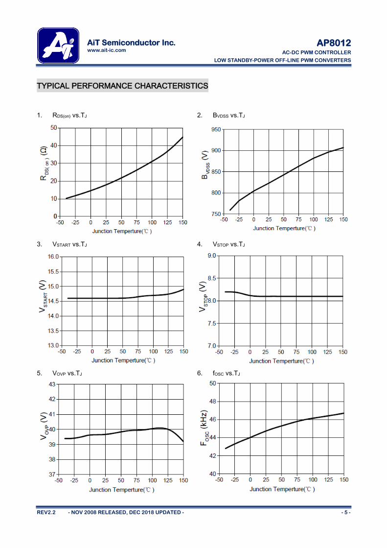
TYPICAL PERFORMANCE CHARACTERISTICS
1. RDS(on) vs.TJ 2. BVDSS vs.TJ
3. VSTART vs.TJ 4. VSTOP vs.TJ
5. VOVP vs.TJ 6. fOSC vs.TJ

AiT Semiconductor Inc. www.ait-ic.com
AP8012
AC-DC PWM CONTROLLER
LOW STANDBY-POWER OFF-LINE PWM CONVERTERS
REV2.2 - NOV 2008 RELEASED, DEC 2018 UPDATED - - 6 -
TYPICAL CIRCUIT
AiT Semiconductor Inc. www.ait-ic.com
AP8012
AC-DC PWM CONTROLLER
LOW STANDBY-POWER OFF-LINE PWM CONVERTERS
REV2.2 - NOV 2008 RELEASED, DEC 2018 UPDATED - - 7 -
DETAILED INFORMATION
Functional Description
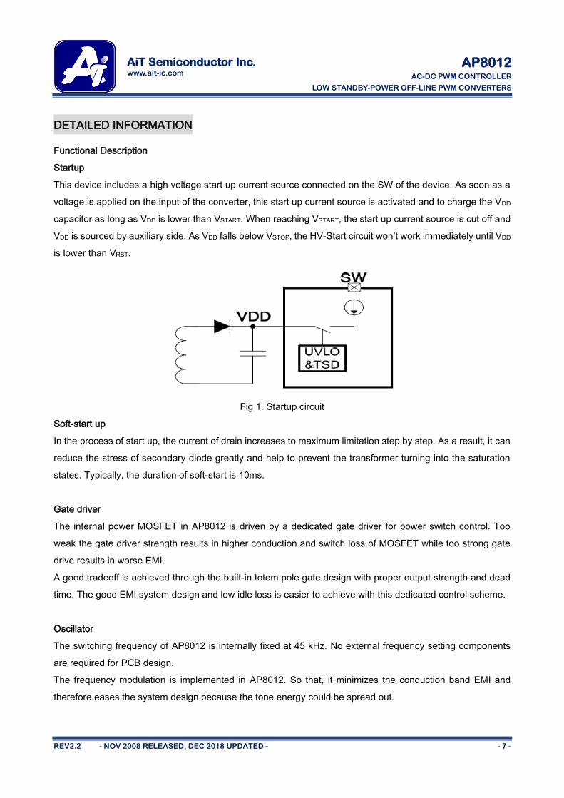
Startup
This device includes a high voltage start up current source connected on the SW of the device. As soon as a
voltage is applied on the input of the converter, this start up current source is activated and to charge the VDD
capacitor as long as VDD is lower than VSTART. When reaching VSTART, the start up current source is cut off and
VDD is sourced by auxiliary side. As VDD falls below VSTOP, the HV-Start circuit won’t work immediately until VDD
is lower than VRST.
Fig 1. Startup circuit
Soft-start up
In the process of start up, the current of drain increases to maximum limitation step by step. As a result, it can
reduce the stress of secondary diode greatly and help to prevent the transformer turning into the saturation
states. Typically, the duration of soft-start is 10ms.
Gate driver
The internal power MOSFET in AP8012 is driven by a dedicated gate driver for power switch control. Too
weak the gate driver strength results in higher conduction and switch loss of MOSFET while too strong gate
drive results in worse EMI.
A good tradeoff is achieved through the built-in totem pole gate design with proper output strength and dead
time. The good EMI system design and low idle loss is easier to achieve with this dedicated control scheme.
Oscillator
The switching frequency of AP8012 is internally fixed at 45 kHz. No external frequency setting components
are required for PCB design.
The frequency modulation is implemented in AP8012. So that, it minimizes the conduction band EMI and
therefore eases the system design because the tone energy could be spread out.
AiT Semiconductor Inc. www.ait-ic.com
AP8012
AC-DC PWM CONTROLLER
LOW STANDBY-POWER OFF-LINE PWM CONVERTERS
REV2.2 - NOV 2008 RELEASED, DEC 2018 UPDATED - - 8 -
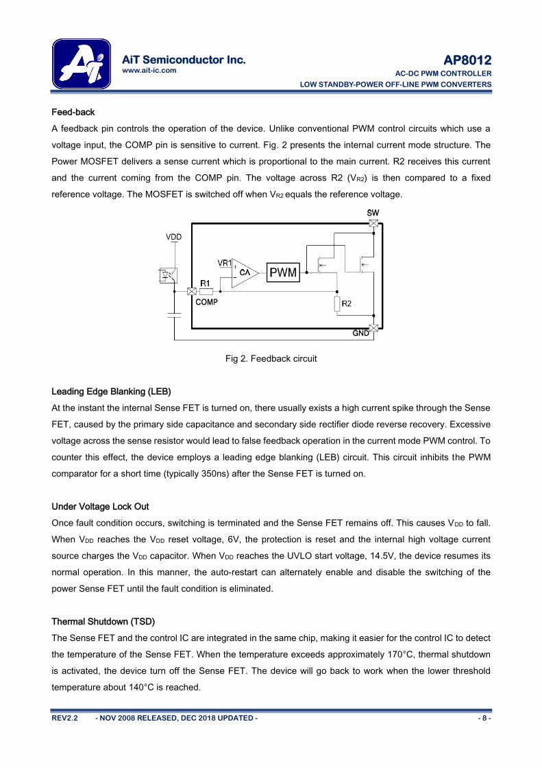
Feed-back
A feedback pin controls the operation of the device. Unlike conventional PWM control circuits which use a
voltage input, the COMP pin is sensitive to current. Fig. 2 presents the internal current mode structure. The
Power MOSFET delivers a sense current which is proportional to the main current. R2 receives this current
and the current coming from the COMP pin. The voltage across R2 (VR2) is then compared to a fixed
reference voltage. The MOSFET is switched off when VR2 equals the reference voltage.
Fig 2. Feedback circuit
Leading Edge Blanking (LEB)
At the instant the internal Sense FET is turned on, there usually exists a high current spike through the Sense
FET, caused by the primary side capacitance and secondary side rectifier diode reverse recovery. Excessive
voltage across the sense resistor would lead to false feedback operation in the current mode PWM control. To
counter this effect, the device employs a leading edge blanking (LEB) circuit. This circuit inhibits the PWM
comparator for a short time (typically 350ns) after the Sense FET is turned on.
Under Voltage Lock Out
Once fault condition occurs, switching is terminated and the Sense FET remains off. This causes VDD to fall.
When VDD reaches the VDD reset voltage, 6V, the protection is reset and the internal high voltage current
source charges the VDD capacitor. When VDD reaches the UVLO start voltage, 14.5V, the device resumes its
normal operation. In this manner, the auto-restart can alternately enable and disable the switching of the
power Sense FET until the fault condition is eliminated.
Thermal Shutdown (TSD)
The Sense FET and the control IC are integrated in the same chip, making it easier for the control IC to detect
the temperature of the Sense FET. When the temperature exceeds approximately 170°C, thermal shutdown
is activated, the device turn off the Sense FET. The device will go back to work when the lower threshold
temperature about 140°C is reached.

AiT Semiconductor Inc. www.ait-ic.com
AP8012
AC-DC PWM CONTROLLER
LOW STANDBY-POWER OFF-LINE PWM CONVERTERS
REV2.2 - NOV 2008 RELEASED, DEC 2018 UPDATED - - 9 -
PACKAGE INFORMATION
Dimension in DIP8 (Unit: mm)
Symbol Min Max
A 3.600 4.000
A1 0.510 -
A2 3.000 3.400
A3 1.550 1.650
b 0.440 0.530
b1 0.430 0.480
B1 1.520BSC
c 0.240 0.320
c1 0.230 0.270
D 9.050 9.450
E1 6.150 6.550
e 2.540BSC
eA 7.620BSC
eB 7.620 9.300
eC 0.000 0.840
L 3.000 -

AiT Semiconductor Inc. www.ait-ic.com
AP8012
AC-DC PWM CONTROLLER
LOW STANDBY-POWER OFF-LINE PWM CONVERTERS
REV2.2 - NOV 2008 RELEASED, DEC 2018 UPDATED - - 10 -
Dimension in SOP8 (Unit: mm)
Symbol Min Max Symbol Min Max
A 1.350 1.750 L 0.450 0.800
A1 0.100 0.250 L1 1.040REF
A2 1.250 1.650 L2 0.250BSC
A3 0.500 0.700 R 0.070 -
b 0.380 0.510 R1 0.070 -
b1 0.370 0.470 h 0.300 0.500
c 0.170 0.250 θ 0° 8°
c1 0.170 0.230 θ1 15° 19°
D 4.800 5.000 θ2 11° 15°
E 5.800 6.200 θ3 15° 19°
E1 3.800 4.000 θ4 11° 15°
e 1.270BSC

AiT Semiconductor Inc. www.ait-ic.com
AP8012
AC-DC PWM CONTROLLER
LOW STANDBY-POWER OFF-LINE PWM CONVERTERS
REV2.2 - NOV 2008 RELEASED, DEC 2018 UPDATED - - 11 -
IMPORTANT NOTICE
AiT Semiconductor Inc. (AiT) reserves the right to make changes to any its product, specifications, to
discontinue any integrated circuit product or service without notice, and advises its customers to obtain the
latest version of relevant information to verify, before placing orders, that the information being relied on is
current.
AiT Semiconductor Inc.'s integrated circuit products are not designed, intended, authorized, or warranted to
be suitable for use in life support applications, devices or systems or other critical applications. Use of AiT
products in such applications is understood to be fully at the risk of the customer. As used herein may involve
potential risks of death, personal injury, or server property, or environmental damage. In order to minimize
risks associated with the customer's applications, the customer should provide adequate design and
operating safeguards.
AiT Semiconductor Inc. assumes to no liability to customer product design or application support. AiT
warrants the performance of its products of the specifications applicable at the time of sale.