Semiconductor Production Equipment - Tokyo Electron
8
8 TOKYO ELECTRON LIMITED Semiconductor Production Equipment Continuous advances in semiconductors are driving the information and without continuous advances in the semiconductor production equipment (SPE) tion by helping chipmakers execute their product strategies successfully. RAPIDLY EXPANDING END-USE APPLICATIONS DRIVE INDUSTRY GROWTH At one time, personal computers were the main end-use application for semiconductors. Today, however, a broad array of products rely on semiconductors to offer increased performance and functionality, including mobile phones, personal digital assistants (PDAs), game consoles, DVD play- ers and other digital consumer electronic products. Furthermore, new, yet-to-be-imagined applica- tions will continue to fuel demand for chips. TOKYO ELECTRON IS A LEADER IN WAFER FABRICATION EQUIPMENT Wafer fabrication equipment uses mainly physical and chemical processes to create minute, multi-layer cir- cuits on round silicon wafers. While various types of equipment are used for performing these microscopic processes, most of these products can be grouped into several broad categories. Most equipment sup- pliers focus on a single market segment, but Tokyo Electron is a world leader in many of them. Thermal Systems Ion Implantation Systems Film Deposition Systems Lithography/Patterning Systems Removal Systems Wafer Fabrication Equipment
-
Upload
khangminh22 -
Category
Documents
-
view
4 -
download
0
Transcript of Semiconductor Production Equipment - Tokyo Electron

8 TOKYO ELECTRON LIMITED
Semiconductor Production EquipmentContinuous advances in semiconductors are driving the information andwithout continuous advances in the semiconductor production equipment (SPE) tion by helping chipmakers execute their product strategies successfully.
RAPIDLY EXPANDING END-USE APPLICATIONS DRIVE INDUSTRY GROWTH
At one time, personal computers were the main end-use application for semiconductors. Today,
however, a broad array of products rely on semiconductors to offer increased performance and
functionality, including mobile phones, personal digital assistants (PDAs), game consoles, DVD play-
ers and other digital consumer electronic products. Furthermore, new, yet-to-be-imagined applica-
tions will continue to fuel demand for chips.
TOKYO ELECTRON IS A LEADER IN
WAFER FABRICATION EQUIPMENT
Wafer fabrication equipment uses mainly physical and
chemical processes to create minute, multi-layer cir-
cuits on round silicon wafers. While various types of
equipment are used for performing these microscopic
processes, most of these products can be grouped
into several broad categories. Most equipment sup-
pliers focus on a single market segment, but Tokyo
Electron is a world leader in many of them.
Thermal Systems
Ion Implantation Systems
Film Deposition Systems
Lithography/Patterning Systems
Removal Systems
Wafer Fabrication Equipment
T O K Y O E L E C T R O N L I M I T E D 9
— The Source of Innovationcommunications revolution. This revolution, however, would not be possible that is used to make chips. Tokyo Electron operates at the heart of this revolu-
SEMICONDUCTOR PRODUCTION EQUIPMENT – A LARGE AND
INTEGRAL PART OF THE SEMICONDUCTOR INDUSTRY
The semiconductor production equipment industry is a large and integral part of the semi-
conductor industry. Information and communications products demand higher perfor-
mance chips from chipmakers, who demand higher performance equipment from equip-
ment suppliers, whose advances drive the information and communications revolution.
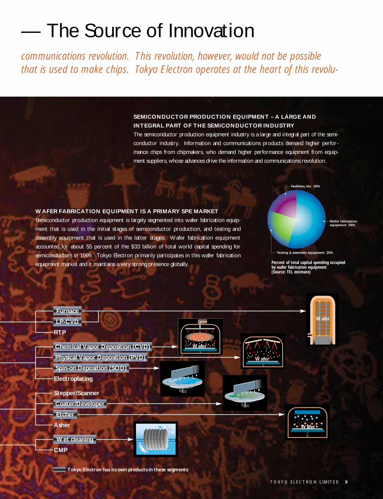
WAFER FABRICATION EQUIPMENT IS A PRIMARY SPE MARKET
Semiconductor production equipment is largely segmented into wafer fabrication equip-
ment that is used in the initial stages of semiconductor production, and testing and
assembly equipment that is used in the latter stages. Wafer fabrication equipment
accounted for about 55 percent of the $33 billion of total world capital spending for
semiconductors in 1999. Tokyo Electron primarily participates in this wafer fabrication
equipment market and it maintains a very strong presence globally.
RTP
Electroplating
Stepper/Scanner
Asher
CMP
Wet cleaning
Coater/Developer
Etcher
Spin-on Deposition (SOD)
Physical Vapor Deposition (PVD)
Furnace
LP-CVD
Chemical Vapor Deposition (CVD)
Percent of total capital spending occupiedby wafer fabrication equipment(Source: TEL estimate)
Facilities, etc. 20%
Wafer fabrication equipment 55%
Testing & assembly equipment 25%
Tokyo Electron has its own products in these segments
Wafer
Wafer
Wafer
Wafer
Calculator Mainframe Desktop PC
Design Rule
Application
10µm 3µm 0.8µm
Wafer Diameter
Front End of LineGate materials
Front End of LineCapacitor materials
Back End of LineInterconnect and Insulator materials
Oxide
Oxide / Nitride
Aluminum + Silicon Dioxide
50mm 75mm 100mm 125mm
1970 1975 1980 1985
10 TOKYO ELECTRON LIMITED
LARGER WAFER SIZEREDUCES UNIT COST OFCHIPSLarger wafers reduce unit costs
because processing a 300mm wafer
costs little more than processing the
current industry standard 200mm
wafer, but the larger wafers yield signifi-
cantly more chips. Tokyo Electron is in
a particularly strong position to capital-
ize on this trend, with a comprehensive
lineup of 300mm-ready equipment, and
a fully dedicated 300mm New Process
Technology Center to support cus-
tomers’ demands in their transition to
300mm technology.
SMALLER FEATURE SIZESINCREASE YIELDS ANDPERFORMANCECurrent feature sizes are approxi-
mately 100 times smaller than they
were just three decades ago, allowing
for smaller, faster chips with substan-
tially increased performance.
Decreasing chip size by shrinking fea-
New Mega Trends Drive SPE DemandThree major trends are taking place simultaneously in the semiconductor industry: – in particular, copper for metalization and low-k (k = dielectric constant) dielectricsSPE to stay at the leading edge of technology. Tokyo Electron already offers proven

Notebook PC Mobile phone
0.5µm 0.35µm 0.25µm 0.18µm 0.13µm
150mm 200mm 300mm
1990 1995 2000 2005
T O K Y O E L E C T R O N L I M I T E D 1 1
ture sizes allows more chips to be
produced from the same wafer. As
the world’s leading supplier of
coater/developers and oxide etch sys-
tems that are directly related to
reducing feature sizes, Tokyo Electron
is well positioned to take advantage of
this trend.
NEW MATERIALS BOOSTCHIP PERFORMANCEIn the 0.13µm generation and beyond,
decreasing signal delay will become crit-
ical in creating faster chips. The solu-
tion to this problem is new materials.
In the early 2000s, two dramatic
changes will begin to take place: the
adoption of high-k and high-ε materials
for gate and capacitor formation in the
FEOL (transistor) process, and
copper and low-k materials as intercon-
nect and insulation materials in the
BEOL (interconnect) process.
Historically strong in providing FEOL
solutions, Tokyo Electron is also work-
ing to provide integrated BEOL solu-
tions around its core spin-on dielectric
system for low-k materials.
the move toward larger 300mm wafers, smaller feature sizes and new materials as insulators. These trends are driving chipmakers to invest in new, highly advancedsolutions for 300mm wafers, smaller feature sizes and low-k dielectrics.
SiON, High-k
High-ε
Copper + Low-k
Car navigation system Game console
PDA
12 TOKYO ELECTRON LIMITED
Tokyo Electron’s Low-k Toolset OffersInterconnect Processes
Breakthrough Technology
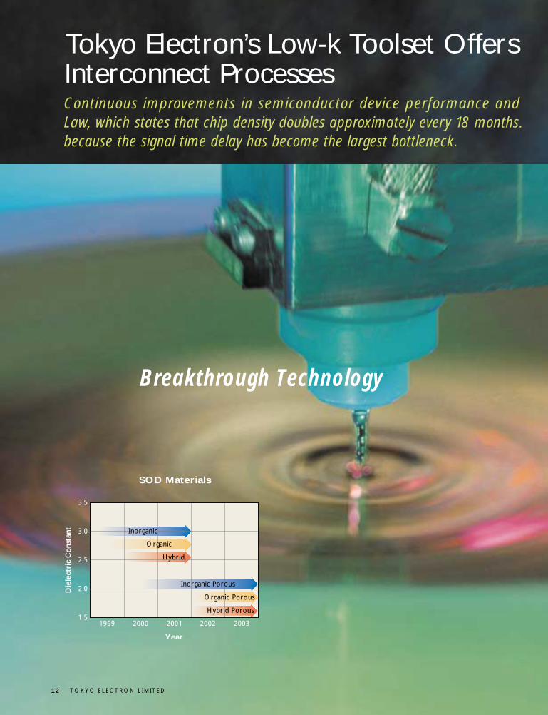
Year
Die
lect
ric
Con
stan
t
SOD Materials
3.5
3.0
2.5
2.0
1.51999 2000 2001 2002 2003
Hybrid
Organic
Inorganic
Hybrid Porous
Organic Porous
Inorganic Porous
Continuous improvements in semiconductor device performance andLaw, which states that chip density doubles approximately every 18 months.because the signal time delay has become the largest bottleneck.
T O K Y O E L E C T R O N L I M I T E D 1 3
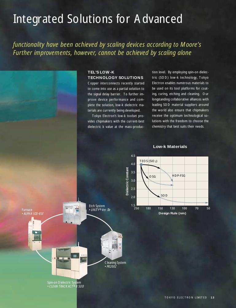
Integrated Solutions for Advanced
Etch System• UNITY® Ver. IIe
Cleaning System• PR200Z
Spin-on Dielectric System• CLEAN TRACK ACT® 8 SOD
Furnace• ALPHA (α)-8SE
TEL’S LOW-KTECHNOLOGY SOLUTIONSCopper interconnects recently started
to come into use as a partial solution to
the signal delay barrier. To further im-
prove device performance and com-
plete the solution, low-k dielectric ma-
terials are currently being developed.
Tokyo Electron's low-k toolset pro-
vides chipmakers with the current-best
dielectric k value at the mass-produc-
tion level. By employing spin-on dielec-
tric (SOD) low-k technology, Tokyo
Electron enables numerous materials to
be used on its tool platforms for coat-
ing, curing, etching and cleaning. Our
longstanding collaborative alliances with
leading SOD material suppliers around
the world also ensure that chipmakers
receive the optimum technological so-
lutions with the freedom to choose the
chemistry that best suits their needs.
Low-k Materials
250 180 150 130 100 70 501.5
2.0
2.5
3.0
3.5
4.0
4.5
Die
lect
ric
Con
stan
t
Design Rule (nm)
SOD
HDP-FSGOSG
TEOS (SiO2)
functionality have been achieved by scaling devices according to Moore’s Further improvements, however, cannot be achieved by scaling alone

14 TOKYO ELECTRON LIMITED
Milestones in Environmental ProtectionTo 1995: Carried out studies for an environmental management system
Eliminated CFC usage
1996: Established first Tokyo Electron Environmental Committee
Implemented environmental management system
1997-1999: Obtained ISO 14001 certification of the environmental
management systems at seven main domestic plants
1999: Created Product EHS Roadmap
2000: Began environmental accounting
Specific Activities
ISO 14001 CertificationTokyo Electron has devoted substantial resources to obtaining ISO 14001 cer-
tification, an international standard for environmental management systems.
The Company began working to obtain this certification in 1997, and obtained
it for all domestic plants by the end of 1999, with the exception of Tokyo
Electron Miyagi Limited. As the certifying body, Tokyo Electron used Det
Norske Veritas (DNV), which has extensive experience in environmental man-
agement and had carried out the Company’s audit for ISO 9001 certification.
Preparations for certification are under way at Tokyo Electron Miyagi Limited,
which began operations in 1998, and the Company is aiming for certification in
April 2002. In the future, Tokyo Electron plans to obtain ISO 14001 certifica-
tion for its U.S. plants.
Development of Environmentally Friendly ProductsTokyo Electron is active in developing products with reduced environmental im-
pact. The CLEAN TRACK ACT® 8 coater/developer and the UW200Z cleaning
system both incorporate new design concepts that significantly reduce footprint,
energy consumption and chemical usage compared with previous models.
Moreover, the Company is conducting R&D with C5F8, a fluorine gas that re-
duces the effects that lead to global warming without any sacrifice in technical
specifications, and is now using it in the etching system process. The C5F8
process received recognition as a method to combat global warming from
E N V I R O N M E N T
A COMMITMENT TO SOCIAL RESPONSIBIL ITY
Tokyo Electron believes that preserving and constantly improving the global environment are objectives of the
highest priority both for the Company and for humanity, and must be considered in management. Based on
this philosophy, we are determined to remain in harmony with the global environment through a wide range
of environmental protection activities as we expand our business. Doing so will help us retain the trust of
customers, shareholders, employees, local communities and society in general.

T O K Y O E L E C T R O N L I M I T E D 1 5
Semiconductor Equipment and Materials International (SEMI) Japan in December
1999. Also in 1999, Tokyo Electron created its Product EHS Roadmap to sup-
port concrete measures to reduce the environmental impact of each system the
Company supplies, in an effort to produce products that are even more environ-
mentally friendly.
Chemical ManagementThe control of chemical substances requires not only compliance with the law,
but also comprehensive management that includes toxicity evaluation and mea-
sures for safe storage and dealing with emergencies. Tokyo Electron is therefore
striving to establish a system for reviewing and registering newly purchased
chemical substances, and is moving forward with a rigorous program to stop pol-
lution before it is produced. Moreover, in April 2000, domestic facilities imple-
mented the Pollutant Release and Transfer Register (PRTR) system, which en-
tails computing the amounts of each listed chemical substance released into the
environment and providing reports to governmental and trade organizations.
Waste Reduction, Recycling and Other ActivitiesDemonstrating the effectiveness of Tokyo Electron’s efforts to reduce waste
products and consumption of energy and resources and to promote recycling
and green purchasing, domestic facilities produced 21 percent less waste in 1998
than in 1997. The Company’s recycling ratio has increased significantly, from
15.3 percent in 1996 to 40.9 percent in 1997 and 49.7 percent in 1998.
Administrative divisions are promoting the purchase of environmentally friendly
paper products, office supplies and printed matter.
Contribution to Customers, Communities and the IndustryTokyo Electron’s proactive efforts to develop environmentally friendly products
make a material contribution to our customers’ efforts to protect the environ-
ment. We also cooperate with environmental initiatives in every region we
serve. In addition, we actively participate at every stage, from planning to imple-
mentation, of industry efforts regarding disclosure and standards. We intend to
further build on our record of corporate citizenship.
Implementation of Environmental Accounting From the year ending March 2001, Tokyo Electron’s domestic operations will
begin using environmental accounting in order to quantify the effectiveness of en-
vironmental protection activities.
DisclosureTokyo Electron will promote broader awareness and understanding of its efforts
to protect the environment by publishing an annual environmental report begin-
ning in 2001.