Aldo Rossi. Ora tutto questo è perduto / All of this is now lost
Upload
khangminh22Category
view
3download
0
To learn more about onsemi™, please visit our website at www.onsemi.com
ON Semiconductor
Is Now
onsemi and and other names, marks, and brands are registered and/or common law trademarks of Semiconductor Components Industries, LLC dba “onsemi” or its affiliates and/or subsidiaries in the United States and/or other countries. onsemi owns the rights to a number of patents, trademarks, copyrights, trade secrets, and other intellectual property. A listing of onsemi product/patent coverage may be accessed at www.onsemi.com/site/pdf/Patent-Marking.pdf. onsemi reserves the right to make changes at any time to any products or information herein, without notice. The information herein is provided “as-is” and onsemi makes no warranty, representation or guarantee regarding the accuracy of the information, product features, availability, functionality, or suitability of its products for any particular purpose, nor does onsemi assume any liability arising out of the application or use of any product or circuit, and specifically disclaims any and all liability, including without limitation special, consequential or incidental damages. Buyer is responsible for its products and applications using onsemi products, including compliance with all laws, regulations and safety requirements or standards, regardless of any support or applications information provided by onsemi. “Typical” parameters which may be provided in onsemi data sheets and/or specifications can and do vary in different applications and actual performance may vary over time. All operating parameters, including “Typicals” must be validated for each customer application by customer’s technical experts. onsemi does not convey any license under any of its intellectual property rights nor the rights of others. onsemi products are not designed, intended, or authorized for use as a critical component in life support systems or any FDA Class 3 medical devices or medical devices with a same or similar classification in a foreign jurisdiction or any devices intended for implantation in the human body. Should Buyer purchase or use onsemi products for any such unintended or unauthorized application, Buyer shall indemnify and hold onsemi and its officers, employees, subsidiaries, affiliates, and distributors harmless against all claims, costs, damages, and expenses, and reasonable attorney fees arising out of, directly or indirectly, any claim of personal injury or death associated with such unintended or unauthorized use, even if such claim alleges that onsemi was negligent regarding the design or manufacture of the part. onsemi is an Equal Opportunity/Affirmative Action Employer. This literature is subject to all applicable copyright laws and is not for resale in any manner. Other names and brands may be claimed as the property of others.

http://onsemi.com1
Zener Theory and Design Considerations
Handbook
HBD854/DRev. 1, Dec−2017
© SCILLC, 2017Previous Edition © 2005“All Rights Reserved’’
http://onsemi.com2
Technical Information, Application Notes and ArticlesZener Diode Theory 3. . . . . . . . . . . . . . . . . . . . . . . . . . . . .Zener Diode Fabrication Techniques 8. . . . . . . . . . . . . . .Reliability 12. . . . . . . . . . . . . . . . . . . . . . . . . . . . . . . . . . . . .Zener Diode Characteristics 18. . . . . . . . . . . . . . . . . . . . .Basic Voltage Regulation Using Zener Diodes 30. . . . .Zener Voltage Sensing Circuits and Applications 40. . .Miscellaneous Applications of Zener Type Devices 44.Measurement of Zener Voltage to Thermal
Equilibrium with Pulsed Test Current 46. . . . . . . . . . .
http://onsemi.com3
ZENER DIODE THEORY
INTRODUCTION
The zener diode is a semiconductor device unique in itsmode of operation and completely unreplaceable by anyother electronic device. Because of its unusual properties itfills a long-standing need in electronic circuitry. It provides,among other useful functions, a constant voltage referenceor voltage control element available over a wide spectrum ofvoltage and power levels.
The zener diode is unique among the semiconductorfamily of devices because its electrical properties arederived from a rectifying junction which operates in thereverse breakdown region. In the sections that follow, thereverse biased rectifying junction, some of the termsassociated with it, and properties derived from it will bediscussed fully.
The zener diode is fabricated from the element silicon(Si). Special techniques are applied in the fabrication ofzener diodes to create the required properties.
This manual was prepared to acquaint the engineer, theequipment designer and manufacturer, and the experimenterwith the fundamental principles, design characteristics,applications and advantages of this importantsemiconductor device.
SEMICONDUCTOR THEORY
The active portion of a zener diode is a semiconductor PNjunction. PN junctions are formed in various kinds ofsemiconductor devices by several techniques. Among theseare the widely used techniques known as alloying anddiffusion which are utilized in fabricating zener PNjunctions to provide excellent control over zener breakdownvoltage.
At the present time, zener diodes use silicon as the basicmaterial in the formation of their PN junction. Silicon is inGroup IV of the periodic table (tetravalent) and is classed asa “semiconductor” due to the fact that it is a poor conductorin a pure state. When controlled amounts of certain“impurities” are added to a semiconductor it becomes abetter conductor of electricity. Depending on the type ofimpurity added to the basic semiconductor, its conductivitymay take two different forms, called P- and N-typerespectively.
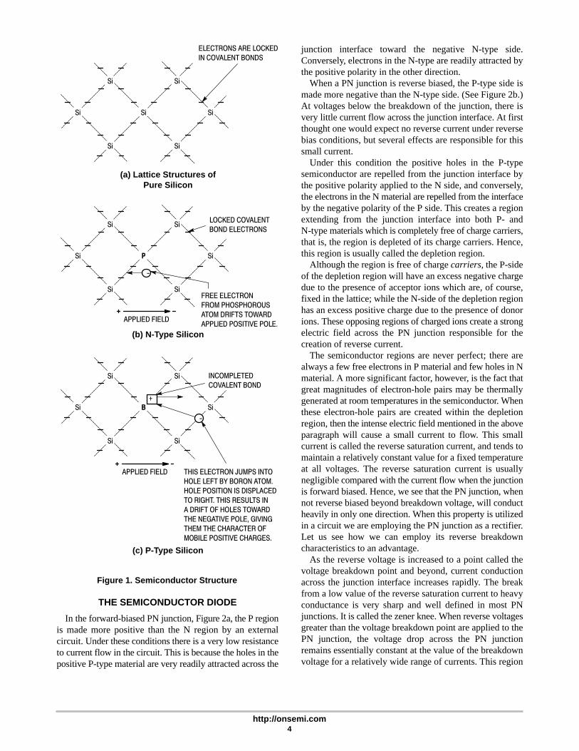
N-type conductivity in a semiconductor is much like theconductivity due to the drift of free electrons in a metal. Inpure silicon at room temperature there are too few freeelectrons to conduct current. However, there are ways ofintroducing free electrons into the crystal lattice as we shall
now see. Silicon is a tetravalent element, one with fourvalence electrons in the outer shell; all are virtually lockedinto place by the covalent bonds of the crystal latticestructure, as shown schematically in Figure 1a. Whencontrolled amounts of donor impurities (Group V elements)such as phosphorus are added, the pentavalent phosphorusatoms entering the lattice structure provide extra electronsnot required by the covalent bonds. These impurities arecalled donor impurities since they “donate” a free electronto the lattice. These donated electrons are free to drift fromnegative to positive across the crystal when a field is applied,as shown in Figure 1b. The “N” nomenclature for this kindof conductivity implies “negative” charge carriers.
In P-type conductivity, the charges that carry electriccurrent across the crystal act as if they were positive charges.We know that electricity is always carried by driftingelectrons in any material, and that there are no mobilepositively charged carriers in a solid. Positive chargecarriers can exist in gases and liquids in the form of positiveions but not in solids. The positive character of the currentflow in the semiconductor crystal may be thought of as themovement of vacancies (called holes) in the covalent lattice.These holes drift from positive toward negative in an electricfield, behaving as if they were positive carriers.
P-type conductivity in semiconductors result from addingacceptor impurities (Group III elements) such as boron tosilicon to the semiconductor crystal. In this case, boronatoms, with three valence electrons, enter the tetravalentsilicon lattice. Since the covalent bonds cannot be satisfiedby only three electrons, each acceptor atom leaves a hole inthe lattice which is deficient by one electron. These holesreadily accept electrons introduced by external sources orcreated by radiation or heat, as shown in Figure 1c. Hencethe name acceptor ion or acceptor impurity. When anexternal circuit is connected, electrons from the currentsource “fill up” these holes from the negative end and jumpfrom hole to hole across the crystal or one may think of thisprocess in a slightly different but equivalent way, that is asthe displacement of positive holes toward the negativeterminal. It is this drift of the positively charged holes whichaccounts for the term P-type conductivity.
When semiconductor regions of N- and P-typeconductivities are formed in a semiconductor crystaladjacent to each other, this structure is called a PN junction.Such a junction is responsible for the action of both zenerdiodes and rectifier devices, and will be discussed in the nextsection.
http://onsemi.com4
Figure 1. Semiconductor Structure
-
Si
Si Si Si
Si
Si Si
Si
Si P Si
Si
Si Si
Si
Si B Si
Si
Si Si
APPLIED FIELD
APPLIED FIELD
+
ELECTRONS ARE LOCKEDIN COVALENT BONDS
LOCKED COVALENTBOND ELECTRONS
FREE ELECTRONFROM PHOSPHOROUSATOM DRIFTS TOWARDAPPLIED POSITIVE POLE.
INCOMPLETEDCOVALENT BOND
THIS ELECTRON JUMPS INTOHOLE LEFT BY BORON ATOM.HOLE POSITION IS DISPLACEDTO RIGHT. THIS RESULTS INA DRIFT OF HOLES TOWARDTHE NEGATIVE POLE, GIVINGTHEM THE CHARACTER OFMOBILE POSITIVE CHARGES.
(a) Lattice Structures ofPure Silicon
(b) N-Type Silicon
(c) P-Type Silicon
-
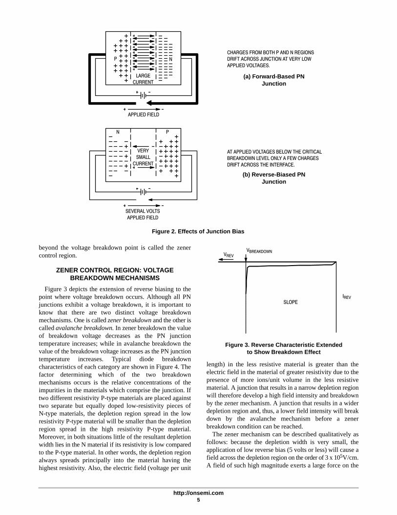
THE SEMICONDUCTOR DIODE
In the forward-biased PN junction, Figure 2a, the P regionis made more positive than the N region by an externalcircuit. Under these conditions there is a very low resistanceto current flow in the circuit. This is because the holes in thepositive P-type material are very readily attracted across the
junction interface toward the negative N-type side.Conversely, electrons in the N-type are readily attracted bythe positive polarity in the other direction.
When a PN junction is reverse biased, the P-type side ismade more negative than the N-type side. (See Figure 2b.)At voltages below the breakdown of the junction, there isvery little current flow across the junction interface. At firstthought one would expect no reverse current under reversebias conditions, but several effects are responsible for thissmall current.
Under this condition the positive holes in the P-typesemiconductor are repelled from the junction interface bythe positive polarity applied to the N side, and conversely,the electrons in the N material are repelled from the interfaceby the negative polarity of the P side. This creates a regionextending from the junction interface into both P- andN-type materials which is completely free of charge carriers,that is, the region is depleted of its charge carriers. Hence,this region is usually called the depletion region.
Although the region is free of charge carriers, the P-sideof the depletion region will have an excess negative chargedue to the presence of acceptor ions which are, of course,fixed in the lattice; while the N-side of the depletion regionhas an excess positive charge due to the presence of donorions. These opposing regions of charged ions create a strongelectric field across the PN junction responsible for thecreation of reverse current.
The semiconductor regions are never perfect; there arealways a few free electrons in P material and few holes in Nmaterial. A more significant factor, however, is the fact thatgreat magnitudes of electron-hole pairs may be thermallygenerated at room temperatures in the semiconductor. Whenthese electron-hole pairs are created within the depletionregion, then the intense electric field mentioned in the aboveparagraph will cause a small current to flow. This smallcurrent is called the reverse saturation current, and tends tomaintain a relatively constant value for a fixed temperatureat all voltages. The reverse saturation current is usuallynegligible compared with the current flow when the junctionis forward biased. Hence, we see that the PN junction, whennot reverse biased beyond breakdown voltage, will conductheavily in only one direction. When this property is utilizedin a circuit we are employing the PN junction as a rectifier.Let us see how we can employ its reverse breakdowncharacteristics to an advantage.
As the reverse voltage is increased to a point called thevoltage breakdown point and beyond, current conductionacross the junction interface increases rapidly. The breakfrom a low value of the reverse saturation current to heavyconductance is very sharp and well defined in most PNjunctions. It is called the zener knee. When reverse voltagesgreater than the voltage breakdown point are applied to thePN junction, the voltage drop across the PN junctionremains essentially constant at the value of the breakdownvoltage for a relatively wide range of currents. This region
http://onsemi.com5
N
APPLIED FIELD
P
LARGECURRENT
SEVERAL VOLTSAPPLIED FIELD
N P
VERYSMALL
CURRENT
Figure 2. Effects of Junction Bias
CHARGES FROM BOTH P AND N REGIONSDRIFT ACROSS JUNCTION AT VERY LOWAPPLIED VOLTAGES.
AT APPLIED VOLTAGES BELOW THE CRITICALBREAKDOWN LEVEL ONLY A FEW CHARGESDRIFT ACROSS THE INTERFACE.
(a) Forward-Based PNJunction
(b) Reverse-Biased PNJunction
beyond the voltage breakdown point is called the zenercontrol region.
ZENER CONTROL REGION: VOLTAGEBREAKDOWN MECHANISMS
Figure 3 depicts the extension of reverse biasing to thepoint where voltage breakdown occurs. Although all PNjunctions exhibit a voltage breakdown, it is important toknow that there are two distinct voltage breakdownmechanisms. One is called zener breakdown and the other iscalled avalanche breakdown. In zener breakdown the valueof breakdown voltage decreases as the PN junctiontemperature increases; while in avalanche breakdown thevalue of the breakdown voltage increases as the PN junctiontemperature increases. Typical diode breakdowncharacteristics of each category are shown in Figure 4. Thefactor determining which of the two breakdownmechanisms occurs is the relative concentrations of theimpurities in the materials which comprise the junction. Iftwo different resistivity P-type materials are placed againsttwo separate but equally doped low-resistivity pieces ofN-type materials, the depletion region spread in the lowresistivity P-type material will be smaller than the depletionregion spread in the high resistivity P-type material.Moreover, in both situations little of the resultant depletionwidth lies in the N material if its resistivity is low comparedto the P-type material. In other words, the depletion regionalways spreads principally into the material having thehighest resistivity. Also, the electric field (voltage per unit
Figure 3. Reverse Characteristic Extendedto Show Breakdown Effect
SLOPEIREV
VBREAKDOWNVREV
length) in the less resistive material is greater than theelectric field in the material of greater resistivity due to thepresence of more ions/unit volume in the less resistivematerial. A junction that results in a narrow depletion regionwill therefore develop a high field intensity and breakdownby the zener mechanism. A junction that results in a widerdepletion region and, thus, a lower field intensity will breakdown by the avalanche mechanism before a zenerbreakdown condition can be reached.
The zener mechanism can be described qualitatively asfollows: because the depletion width is very small, theapplication of low reverse bias (5 volts or less) will cause afield across the depletion region on the order of 3 x 10⁵V/cm.A field of such high magnitude exerts a large force on the
http://onsemi.com6
Figure 4. Typical Breakdown Diode Characteristics. Note Effects of Temperature for Each Mechanism
(A)
ZENER BREAKDOWNOF A PN FUNCTION
VREV (VOLTS)
(B)
AVALANCHE BREAKDOWN OF A PN FUNCTION
IREV IREV
4 3 2 1
VREV (VOLTS)
30 25 20 15 10 5
25°C 65°C 25°C65°C
valence electrons of a silicon atom, tending to separate themfrom their respective nuclei. Actual rupture of the covalentbonds occurs when the field approaches 3 x 10⁵V/cm. Thus,electron-hole pairs are generated in large numbers and asudden increase of current is observed. Although we speakof a rupture of the atomic structure, it should be understoodthat this generation of electron-hole pairs may be carried oncontinuously as long as an external source suppliesadditional electrons. If a limiting resistance in the circuitexternal to the diode junction does not prevent the currentfrom increasing to high values, the device may be destroyeddue to overheating. The actual critical value of field causingzener breakdown is believed to be approximately3 x 105V/cm. On most commercially available silicondiodes, the maximum value of voltage breakdown by thezener mechanism is 8 volts. In order to fabricate deviceswith higher voltage breakdown characteristics, materialswith higher resistivity, and consequently, wider depletionregions are required. These wide depletion regions hold thefield strength down below the zener breakdown value(3 x 10⁵V/cm). Consequently, for devices with breakdownvoltage lower than 5 volts the zener mechanismpredominates, between 5 and 8 volts both zener and anavalanche mechanism are involved, while above 8 volts theavalanche mechanism alone takes over.
The decrease of zener breakdown voltage as junctiontemperature increases can be explained in terms of theenergies of the valence electrons. An increase of temperatureincreases the energies of the valence electrons. This weakensthe bonds holding the electrons and consequently, less appliedvoltage is necessary to pull the valence electrons from theirposition around the nuclei. Thus, the breakdown voltagedecreases as the temperature increases.
The dependence on temperature of the avalanchebreakdown mechanism is quite different. Here the depletionregion is of sufficient width that the carriers (electrons orholes) can suffer collisions before traveling the regioncompletely i.e., the depletion region is wider than onemean-free path (the average distance a carrier can travel
before combining with a carrier of opposite conductivity).Therefore, when temperature is increased, the increasedlattice vibration shortens the distance a carrier travels beforecolliding and thus requires a higher voltage to get it acrossthe depletion region.
As established earlier, the applied reverse bias causes asmall movement of intrinsic electrons from the P material tothe potentially positive N material and intrinsic holes fromthe N material to the potentially negative P material (leakagecurrent). As the applied voltage becomes larger, theseelectrons and holes increasingly accelerate. There are alsocollisions between these intrinsic particles and boundelectrons as the intrinsic particles move through thedepletion region. If the applied voltage is such that theintrinsic electrons do not have high velocity, then thecollisions take some energy from the intrinsic particles,altering their velocity. If the applied voltage is increased,collision with a valence electron will give considerableenergy to the electron and it will break free of its covalentbond. Thus, one electron by collision, has created anelectron-hole pair. These secondary particles will also beaccelerated and participate in collisions which generate newelectron-hole pairs. This phenomenon is called carriermultiplication. Electron-hole pairs are generated so quicklyand in such large numbers that there is an apparent avalancheor self-sustained multiplication process (depictedgraphically in Figure 5). The junction is said to be inbreakdown and the current is limited only by resistanceexternal to the junction. Zener diodes above 7 to 8 voltsexhibit avalanche breakdown.
As junction temperature increases, the voltage breakdownpoint for the avalanche mechanism increases. This effect canbe explained by considering the vibration displacement ofatoms in their lattice increases, and this increaseddisplacement corresponds to an increase in the probabilitythat intrinsic particles in the depletion region will collidewith the lattice atoms. If the probability of an intrinsicparticle-atom collision increases, then the probability that agiven intrinsic particle will obtain high momentum
http://onsemi.com7
Figure 5. PN Junction in Avalanche Breakdown
WHEN THE APPLIED VOLTAGE IS ABOVE THE BREAKDOWN POINT, A FEW INJECTED ELECTRONS RECEIVE ENOUGH ACCELERATION FROM THE FIELD TO GENERATE NEW ELECTRONS BY COLLISION. DURING THIS PROCESS THE VOLTAGE DROP ACROSS THE JUNCTION REMAINS CONSTANT.
RS ABSORBS EXCESS VOLTAGE.
R
S
N P
LARGE CURRENT
CONSTANT VOLTAGE DROP
REVERSE‐BIASEDPN JUNCTION IN AVALANCHE
decreases, and it follows that the low momentum intrinsicparticles are less likely to ionize the lattice atoms. Naturally,increased voltage increases the acceleration of the intrinsicparticles, providing higher mean momentum and moreelectron-hole pairs production. If the voltage is raisedsufficiently, the mean momentum becomes great enough tocreate electron-hole pairs and carrier multiplication results.Hence, for increasing temperature, the value of theavalanche breakdown voltage increases.
VOLT-AMPERE CHARACTERISTICS
The zener volt-ampere characteristics for a typical 30 voltzener diode is illustrated in Figure 6. It shows that the zenerdiode conducts current in both directions; the forwardcurrent IF being a function of forward voltage VF. Note thatIF is small until VF ≈ 0.65 V; then IF increases very rapidly.For VF > 0.65 V IF is limited primarily by the circuitresistance external to the diode.
ZZK
VZ
ZZT
IR
30 20 10 0 0.5 1 1.5
15
10
5
0
0.5
1
1.5
REVERSECHARACTERISTIC
VR(VOLTS)
VF(VOLTS)
I (
AMPS
)F
REV
ERSE
CU
RR
ENT
(AM
PS)
Figure 6. Zener Diode Characteristics
IZT
IZM
1.40 A
IZK = 5 mA
FORWARDCHARACTERISTIC TYPICAL
420 mA
The reverse current is a function of the reverse voltage VRbut for most practical purposes is zero until the reversevoltage approaches VZ, the PN junction breakdown voltage,at which time the reverse current increases very rapidly.Since the reverse current is small for VR < VZ, but great forVR > VZ each of the current regions is specified by adifferent symbol. For the leakage current region, i.e.
non-conducting region, between 0 volts and VZ, the reversecurrent is denoted by the symbol IR; but for the zener controlregion, VR ≥ VZ, the reverse current is denoted by thesymbol IZ. IR is usually specified at a reverse voltageVR ≈ 0.8 VZ.
The PN junction breakdown voltage, VZ, is usually calledthe zener voltage, regardless whether the diode is of thezener or avalanche breakdown type. Commercial zenerdiodes are available with zener voltages from about1.8 V − 400 V. For most applications the zener diode isoperated well into the breakdown region (IZT to IZM). Mostmanufacturers give an additional specification of IZK(= 5 mA in Figure 6) to indicate a minimum operatingcurrent to assure reasonable regulation.
This minimum current IZK varies in the various types ofzener diodes and, consequently, is given on the data sheets.The maximum zener current IZM should be considered themaximum reverse current recommended by themanufacturer. Values of IZM are usually given in the datasheets.
Between the limits of IZK and IZM, which are 5 mA and1400 mA (1.4 Amps) in the example of Figure 6, the voltageacross the diode is essentially constant, and ≈ VZ. Thisplateau region has, however, a large positive slope such thatthe precise value of reverse voltage will change slightly asa function of IZ. For any point on this plateau region one maycalculate an impedance using the incremental magnitudes ofthe voltage and current. This impedance is usually called thezener impedance ZZ, and is specified for most zener diodes.Most manufacturers measure the maximum zenerimpedance at two test points on the plateau region. The firstis usually near the knee of the zener plateau, ZZK, and thelatter point near the midrange of the usable zener currentexcursion. Two such points are illustrated in Figure 6.
This section was intended to introduce the reader to a fewof the major terms used with zener diodes. A completedescription of these terms may be found in the zener diodecharacteristic section. In this section a full discussion ofzener leakage, DC breakdown, zener impedance,temperature coefficients and many other topics may befound.
http://onsemi.com8
ZENER DIODE FABRICATION TECHNIQUES
INTRODUCTION
A brief exposure to the techniques used in the fabricationof zener diodes can provide the engineer with additionalinsight using zeners in their applications. That is, anunderstanding of zener fabrication makes the capabilitiesand limitations of the zener diode more meaningful. Thissection discusses the basic steps in the fabrication of thezener from crystal growing through final testing.
ZENER DIODE WAFER FABRICATION
The major steps in the manufacture of zeners are providedin the process flow in Figure 1. It is important to point outthat the manufacturing steps vary somewhat frommanufacturer to manufacturer, and also vary with the type ofzener diode produced. This is driven by the type of packagerequired as well as the electrical characteristics desired. Forexample, alloy diffused devices provide excellent lowvoltage reference with low leakage characteristics but do not
have the same surge carrying capability as diffused diodes.The manufacturing process begins with the growing of highquality silicon crystals.
Crystals for ON Semiconductor zener diodes are grownusing the Czochralski technique, a widely used processwhich begins with ultra-pure polycrystalline silicon. Thepolycrystalline silicon is first melted in a nonreactivecrucible held at a temperature just above the melting point.A carefully controlled quantity of the desired dopantimpurity, such as phosphorus or boron is added. A highquality seed crystal of the desired crystalline orientation isthen lowered into the melt while rotating. A portion of thisseed crystal is allowed to melt into the molten silicon. Theseed is then slowly pulled and continues to rotate as it israised from the melt. As the seed is raised, cooling takesplace and material from the melt adheres to it, thus forminga single crystal ingot. With this technique, ingots withdiameters of several inches can be fabricated.
Figure 1. General Flow of the Zener Diode Process
SILICON CRYSTALGROWING
WAFERPREPARATION
OXIDEPASSIVATION
WAFER THINNINGANODE
METALLIZATIONJUNCTION
FORMATION
CATHODEMETALLIZATION
WAFERTESTING
WAFER DICING
TESTLEAD
FINISHASSEMBLY
MARK TEST PACKAGE
SHIP
http://onsemi.com9
Figure 2. Basic Fabrication Steps in the Silicon Planar Process: a) oxide formation, b) selective oxide removal,c) deposition of dopant atoms, d) junction formation by diffusion of dopant atoms.
SILICON DIOXIDE GROWTH
SiO2
Si
(a)
SILICON DIOXIDE SELECTIVELY REMOVED
(b)
(c)
DOPANT ATOMS DEPOSITED ONTOTHE EXPOSED SILICON
(d)
DOPANT ATOMS DIFFUSE INTO SILICONBUT NOT APPRECIABLY INTO THE SILICON DIOXIDE
Once the single-crystal silicon ingot is grown, it is testedfor doping concentration (resistivity), undesired impuritylevels, and minority carrier lifetime. The ingot is then slicedinto thin, circular wafers. The wafers are then chemicallyetched to remove saw damage and polished in a sequence ofsuccessively finer polishing grits until a mirror-like defectfree surface is obtained. The wafers are then cleaned andplaced in vacuum sealed wafer carriers to prevent anycontamination from getting on them. At this point, thewafers are ready to begin device fabrication.
Zener diodes can be manufactured using differentprocessing techniques such as planar processing or mesaetched processing. The majority of ON Semiconductorzener diodes are manufactured using the planar technique asshown in Figure 2.
The planar process begins by growing an ultra-cleanprotective silicon dioxide passivation layer. The oxide istypically grown in the temperature range of 900 to 1200degrees celcius. Once the protective layer of silicon dioxidehas been formed, it must be selectively removed from thoseareas into which dopant atoms will be introduced. This isdone using photolithographic techniques.
First a light sensitive solution called photo resist is spunonto the wafer. The resist is then dried and a photographicnegative or mask is placed over the wafer. The resist is thenexposed to ultraviolet light causing the molecules in it tocross link or polymerize becoming very rigid. Those areasof the wafer that are protected by opaque portions of themask are not exposed and are developed away. The oxide isthen etched forming the exposed regions in which the dopantwill be introduced. The remaining resist is then removed andthe wafers carefully cleaned for the doping steps.
Dopant is then introduced onto the wafer surface usingvarious techniques such as aluminum alloy for low voltagedevices, ion-implantation, spin-on dopants, or chemicalvapor deposition. Once the dopant is deposited, thejunctions are formed in a subsequent high temperature (1100to 1250 degrees celcius are typical) drive-in. The resultantjunction profile is determined by the backgroundconcentration of the starting substrate, the amount of dopantplaced at the surface, and amount of time and temperatureused during the dopant drive-in. This junction profiledetermines the electrical characteristics of the device.During the drive-in cycle, additional passivation oxide isgrown providing additional protection for the devices.
After junction formation, the wafers are then processedthrough what is called a getter process. The getter steputilizes high temperature and slight stress provided by ahighly doped phosphosilicate glass layer introduced into thebackside of the wafers. This causes any contaminants in thearea of the junction to diffuse away from the region. Thisserves to improve the reverse leakage characteristic and thestability of the device. Following the getter process, a secondphoto resist step opens the contact area in which the anodemetallization is deposited.
Metal systems for ON Semiconductor’s zener diodes aredetermined by the requirements of the package. The metalsystems are deposited in ultra-clean vacuum chambersutilizing electron-beam evaporation techniques. Once themetal is deposited, photo resist processing is utilized to formthe desired patterns. The wafers are then lapped to their finalthickness and the cathode metallization deposited using thesame e-beam process.
http://onsemi.com10
The quality of the wafers is closely monitored throughoutthe process by using statistical process control techniquesand careful microscopic inspections at critical steps. Specialwafer handling equipment is used throughout themanufacturing process to minimize contamination and toavoid damaging the wafers in any way. This furtherenhances the quality and stability of the devices.
Upon completion of the fabrication steps, the wafers areelectrically probed, inspected, and packaged for shipment tothe assembly operations. All ON Semiconductor zenerdiode product is sawn using 100% saw-through techniquesstringently developed to provide high quality silicon die.
ZENER DIODE ASSEMBLY
Surmetic 40
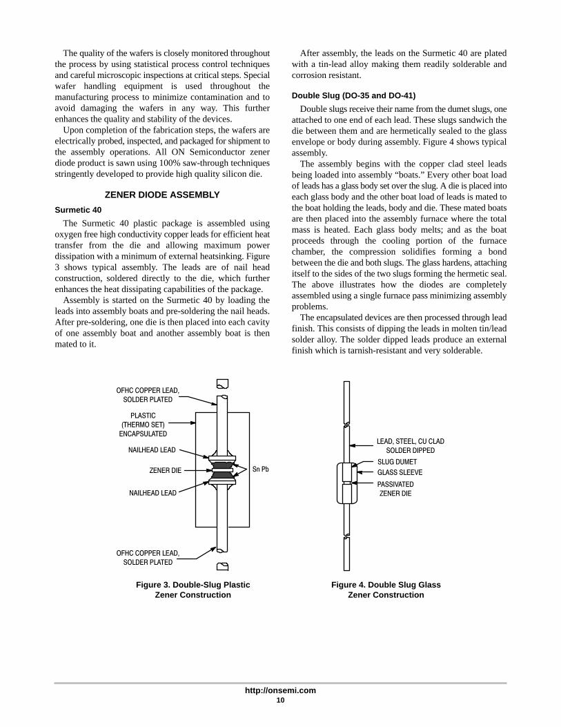
The Surmetic 40 plastic package is assembled usingoxygen free high conductivity copper leads for efficient heattransfer from the die and allowing maximum powerdissipation with a minimum of external heatsinking. Figure3 shows typical assembly. The leads are of nail headconstruction, soldered directly to the die, which furtherenhances the heat dissipating capabilities of the package.
Assembly is started on the Surmetic 40 by loading theleads into assembly boats and pre-soldering the nail heads.After pre-soldering, one die is then placed into each cavityof one assembly boat and another assembly boat is thenmated to it.
After assembly, the leads on the Surmetic 40 are platedwith a tin-lead alloy making them readily solderable andcorrosion resistant.
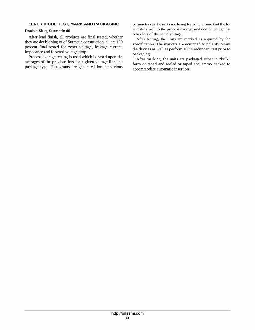
Double Slug (DO-35 and DO-41)
Double slugs receive their name from the dumet slugs, oneattached to one end of each lead. These slugs sandwich thedie between them and are hermetically sealed to the glassenvelope or body during assembly. Figure 4 shows typicalassembly.
The assembly begins with the copper clad steel leadsbeing loaded into assembly “boats.” Every other boat loadof leads has a glass body set over the slug. A die is placed intoeach glass body and the other boat load of leads is mated tothe boat holding the leads, body and die. These mated boatsare then placed into the assembly furnace where the totalmass is heated. Each glass body melts; and as the boatproceeds through the cooling portion of the furnacechamber, the compression solidifies forming a bondbetween the die and both slugs. The glass hardens, attachingitself to the sides of the two slugs forming the hermetic seal.The above illustrates how the diodes are completelyassembled using a single furnace pass minimizing assemblyproblems.
The encapsulated devices are then processed through leadfinish. This consists of dipping the leads in molten tin/leadsolder alloy. The solder dipped leads produce an externalfinish which is tarnish-resistant and very solderable.
Figure 3. Double-Slug PlasticZener Construction
Figure 4. Double Slug GlassZener Construction
OFHC COPPER LEAD,SOLDER PLATED
PLASTIC(THERMO SET)
ENCAPSULATED
NAILHEAD LEAD
ZENER DIE Sn Pb
OFHC COPPER LEAD,SOLDER PLATED
LEAD, STEEL, CU CLADSOLDER DIPPED
SLUG DUMETGLASS SLEEVE
PASSIVATEDZENER DIENAILHEAD LEAD
http://onsemi.com11
ZENER DIODE TEST, MARK AND PACKAGING
Double Slug, Surmetic 40
After lead finish, all products are final tested, whetherthey are double slug or of Surmetic construction, all are 100percent final tested for zener voltage, leakage current,impedance and forward voltage drop.
Process average testing is used which is based upon theaverages of the previous lots for a given voltage line andpackage type. Histograms are generated for the various
parameters as the units are being tested to ensure that the lotis testing well to the process average and compared againstother lots of the same voltage.
After testing, the units are marked as required by thespecification. The markers are equipped to polarity orientthe devices as well as perform 100% redundant test prior topackaging.
After marking, the units are packaged either in “bulk”form or taped and reeled or taped and ammo packed toaccommodate automatic insertion.
http://onsemi.com12
RELIABILITY
INTRODUCTION
ON Semiconductor’s Quality System maintains“continuous product improvement” goals in all phases of theoperation. Statistical process control (SPC), quality controlsampling, reliability audits and accelerated stress testingtechniques monitor the quality and reliability of its products.Management and engineering skills are continuouslyupgraded through training programs. This maintains aunified focus on Six Sigma quality and reliability from theinception of the product to final customer use.
STATISTICAL PROCESS CONTROL
ON Semiconductor’s Discrete Group is continuallypursuing new ways to improve product quality. Initial designimprovement is one method that can be used to produce asuperior product. Equally important to outgoing productquality is the ability to produce product that consistentlyconforms to specification. Process variability is the basicenemy of semiconductor manufacturing since it leads toproduct variability. Used in all phases ofON Semiconductor’s product manufacturing,STATISTICAL PROCESS CONTROL (SPC) replacesvariability with predictability. The traditional philosophy inthe semiconductor industry has been adherence to the datasheet specification. Using SPC methods assures the productwill meet specific process requirements throughout themanufacturing cycle. The emphasis is on defect prevention,not detection. Predictability through SPC methods requiresthe manufacturing culture to focus on constant andpermanent improvements. Usually these improvementscannot be bought with state-of-the-art equipment orautomated factories. With quality in design, process andmaterial selection, coupled with manufacturingpredictability, ON Semiconductor can produce world classproducts.
The immediate effect of SPC manufacturing ispredictability through process controls. Product centered anddistributed well within the product specification benefits ONSemiconductor with fewer rejects, improved yields and lowercost. The direct benefit to ON Semiconductor’s customersincludes better incoming quality levels, less inspection timeand ship-to-stock capability. Circuit performance is oftendependent on the cumulative effect of component variability.Tightly controlled component distributions give the customergreater circuit predictability. Many customers are alsoconverting to just-in-time (JIT) delivery programs. Theseprograms require improvements in cycle time and yieldpredictability achievable only through SPC techniques. Thebenefit derived from SPC helps the manufacturer meet thecustomer’s expectations of higher quality and lower costproduct.
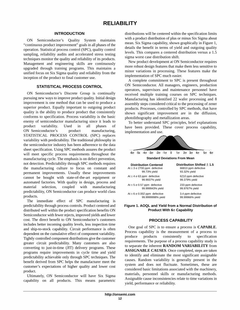
Ultimately, ON Semiconductor will have Six Sigmacapability on all products. This means parametric
distributions will be centered within the specification limitswith a product distribution of plus or minus Six Sigma aboutmean. Six Sigma capability, shown graphically in Figure 1,details the benefit in terms of yield and outgoing qualitylevels. This compares a centered distribution versus a 1.5sigma worst case distribution shift.
New product development at ON Semiconductor requiresmore robust design features that make them less sensitive tominor variations in processing. These features make theimplementation of SPC much easier.
A complete commitment to SPC is present throughoutON Semiconductor. All managers, engineers, productionoperators, supervisors and maintenance personnel havereceived multiple training courses on SPC techniques.Manufacturing has identified 22 wafer processing and 8assembly steps considered critical to the processing of zenerproducts. Processes, controlled by SPC methods, that haveshown significant improvement are in the diffusion,photolithography and metallization areas.
To better understand SPC principles, brief explanationshave been provided. These cover process capability,implementation and use.
Figure 1. AOQL and Yield from a Normal Distribution ofProduct With 6σ Capability
Standard Deviations From Mean
Distribution Centered Distribution Shifted ± 1.5At ± 3 σ 2700 ppm defective
99.73% yield
At ± 4 σ 63 ppm defective99.9937% yield
At ± 5 σ 0.57 ppm defective99.999943% yield
At ± 6 σ 0.002 ppm defective99.9999998% yield
66810 ppm defective93.32% yield
6210 ppm defective99.379% yield
233 ppm defective99.9767% yield
3.4 ppm defective99.99966% yield
�‐6σ �‐5s �‐4σ �‐3σ �‐2σ �‐1σ �0 �1σ �2σ �3σ �4σ �5σ �6σ
PROCESS CAPABILITY
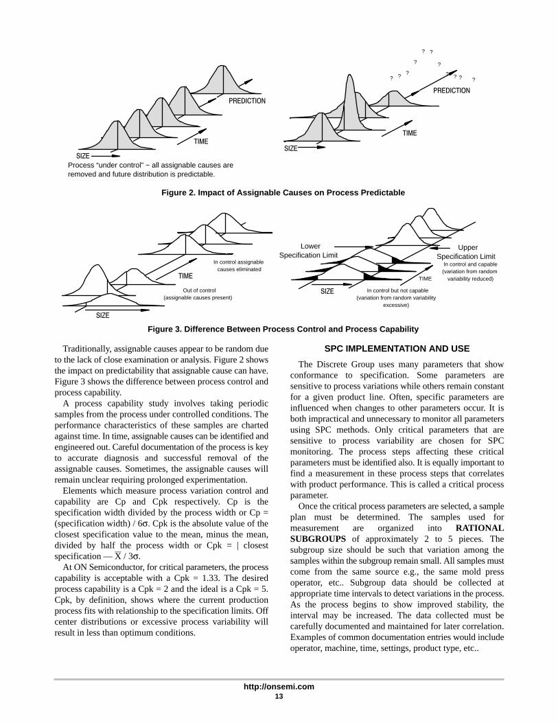
One goal of SPC is to ensure a process is CAPABLE.Process capability is the measurement of a process toproduce products consistently to specificationrequirements. The purpose of a process capability study isto separate the inherent RANDOM VARIABILITY fromASSIGNABLE CAUSES. Once completed, steps are takento identify and eliminate the most significant assignablecauses. Random variability is generally present in thesystem and does not fluctuate. Sometimes, these areconsidered basic limitations associated with the machinery,materials, personnel skills or manufacturing methods.Assignable cause inconsistencies relate to time variations inyield, performance or reliability.
http://onsemi.com13
Figure 2. Impact of Assignable Causes on Process Predictable
Figure 3. Difference Between Process Control and Process Capability
??
?
??
?
???
Process “under control” − all assignable causes areremoved and future distribution is predictable.
PREDICTION
TIME
SIZESIZE
TIME
PREDICTION
SIZE
TIME
Out of control(assignable causes present)
In control assignable causes eliminated
SIZE
TIME
In control but not capable(variation from random variability
excessive)
LowerSpecification Limit
UpperSpecification Limit
In control and capable(variation from random
variability reduced)
? ?
Traditionally, assignable causes appear to be random dueto the lack of close examination or analysis. Figure 2 showsthe impact on predictability that assignable cause can have.Figure 3 shows the difference between process control andprocess capability.
A process capability study involves taking periodicsamples from the process under controlled conditions. Theperformance characteristics of these samples are chartedagainst time. In time, assignable causes can be identified andengineered out. Careful documentation of the process is keyto accurate diagnosis and successful removal of theassignable causes. Sometimes, the assignable causes willremain unclear requiring prolonged experimentation.
Elements which measure process variation control andcapability are Cp and Cpk respectively. Cp is thespecification width divided by the process width or Cp =(specification width) / 6σ. Cpk is the absolute value of theclosest specification value to the mean, minus the mean,divided by half the process width or Cpk = | closestspecification — X / 3σ.
At ON Semiconductor, for critical parameters, the processcapability is acceptable with a Cpk = 1.33. The desiredprocess capability is a Cpk = 2 and the ideal is a Cpk = 5.Cpk, by definition, shows where the current productionprocess fits with relationship to the specification limits. Offcenter distributions or excessive process variability willresult in less than optimum conditions.
SPC IMPLEMENTATION AND USE
The Discrete Group uses many parameters that showconformance to specification. Some parameters aresensitive to process variations while others remain constantfor a given product line. Often, specific parameters areinfluenced when changes to other parameters occur. It isboth impractical and unnecessary to monitor all parametersusing SPC methods. Only critical parameters that aresensitive to process variability are chosen for SPCmonitoring. The process steps affecting these criticalparameters must be identified also. It is equally important tofind a measurement in these process steps that correlateswith product performance. This is called a critical processparameter.
Once the critical process parameters are selected, a sampleplan must be determined. The samples used formeasurement are organized into RATIONALSUBGROUPS of approximately 2 to 5 pieces. Thesubgroup size should be such that variation among thesamples within the subgroup remain small. All samples mustcome from the same source e.g., the same mold pressoperator, etc.. Subgroup data should be collected atappropriate time intervals to detect variations in the process.As the process begins to show improved stability, theinterval may be increased. The data collected must becarefully documented and maintained for later correlation.Examples of common documentation entries would includeoperator, machine, time, settings, product type, etc..
http://onsemi.com14
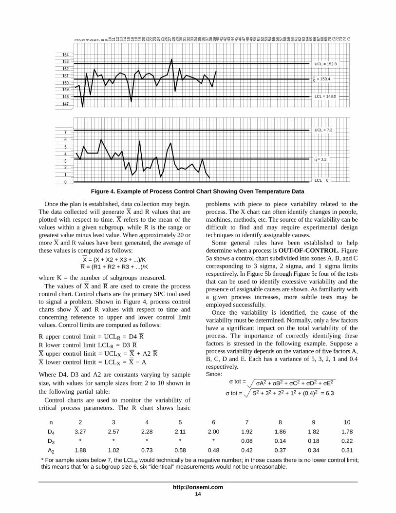
Figure 4. Example of Process Control Chart Showing Oven Temperature Data
147
148
149150
151
152
153
154
1 2 3 4 5 6 7 8 9 10 11 12 13 14 15 16 18 19 20 21 22 23 24 25 26 27 28 29 30 31 32 33 34 35 36 37 38 39 40 41 42 43 44 45 46 47 48 49 50 51 52 53 54 55 56 57 58 59 60 61 62 63 64 65 66 67 68 69 70 71 72 73 74 75
0
1
23
4
5
6
7
UCL = 152.8
= 150.4
LCL = 148.0
UCL = 7.3
= 3.2
LCL = 0
X
R
Once the plan is established, data collection may begin.The data collected will generate X and R values that areplotted with respect to time. X refers to the mean of thevalues within a given subgroup, while R is the range orgreatest value minus least value. When approximately 20 ormore X and R values have been generated, the average ofthese values is computed as follows:
X = (X + X2 + X3 + ...)/KR = (R1 + R2 + R3 + ...)/K
where K = the number of subgroups measured.The values of X and R are used to create the process
control chart. Control charts are the primary SPC tool usedto signal a problem. Shown in Figure 4, process controlcharts show X and R values with respect to time andconcerning reference to upper and lower control limitvalues. Control limits are computed as follows:
R upper control limit = UCLR = D4 RR lower control limit LCLR = D3 RX upper control limit = UCLX = X + A2 RX lower control limit = LCLX = X − A
Where D4, D3 and A2 are constants varying by samplesize, with values for sample sizes from 2 to 10 shown inthe following partial table:
Control charts are used to monitor the variability ofcritical process parameters. The R chart shows basic
problems with piece to piece variability related to theprocess. The X chart can often identify changes in people,machines, methods, etc. The source of the variability can bedifficult to find and may require experimental designtechniques to identify assignable causes.
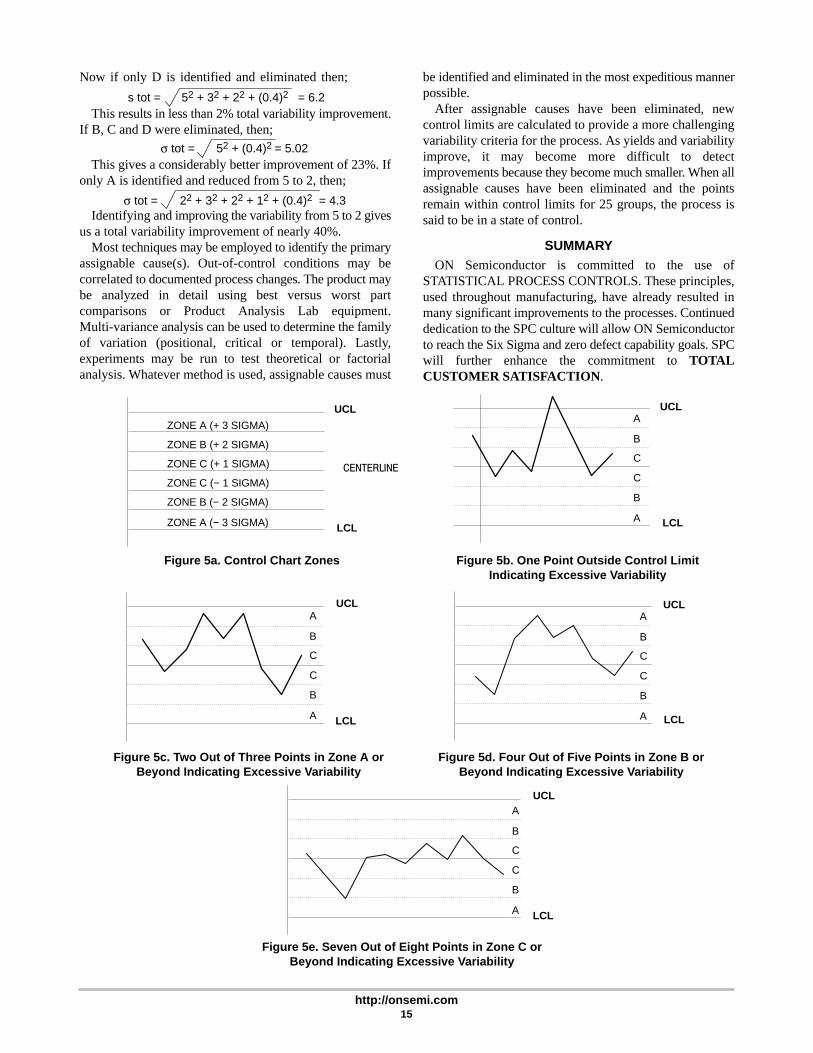
Some general rules have been established to helpdetermine when a process is OUT-OF-CONTROL. Figure5a shows a control chart subdivided into zones A, B, and Ccorresponding to 3 sigma, 2 sigma, and 1 sigma limitsrespectively. In Figure 5b through Figure 5e four of the teststhat can be used to identify excessive variability and thepresence of assignable causes are shown. As familiarity witha given process increases, more subtle tests may beemployed successfully.
Once the variability is identified, the cause of thevariability must be determined. Normally, only a few factorshave a significant impact on the total variability of theprocess. The importance of correctly identifying thesefactors is stressed in the following example. Suppose aprocess variability depends on the variance of five factors A,B, C, D and E. Each has a variance of 5, 3, 2, 1 and 0.4respectively.Since:
σ tot = σA2 + σB2 + σC2 + σD2 + σE2
σ tot = 52 + 32 + 22 + 12 + (0.4)2 = 6.3
n 2 3 4 5 6 7 8 9 10
D4 3.27 2.57 2.28 2.11 2.00 1.92 1.86 1.82 1.78
D3 * * * * * 0.08 0.14 0.18 0.22
A2 1.88 1.02 0.73 0.58 0.48 0.42 0.37 0.34 0.31
* For sample sizes below 7, the LCLR would technically be a negative number; in those cases there is no lower control limit;this means that for a subgroup size 6, six “identical” measurements would not be unreasonable.
http://onsemi.com15
Now if only D is identified and eliminated then;
s tot = 52 + 32 + 22 + (0.4)2 = 6.2This results in less than 2% total variability improvement.
If B, C and D were eliminated, then;
σ tot = 52 + (0.4)2 = 5.02This gives a considerably better improvement of 23%. If
only A is identified and reduced from 5 to 2, then;
σ tot = 22 + 32 + 22 + 12 + (0.4)2 = 4.3Identifying and improving the variability from 5 to 2 gives
us a total variability improvement of nearly 40%.Most techniques may be employed to identify the primary
assignable cause(s). Out-of-control conditions may becorrelated to documented process changes. The product maybe analyzed in detail using best versus worst partcomparisons or Product Analysis Lab equipment.Multi-variance analysis can be used to determine the familyof variation (positional, critical or temporal). Lastly,experiments may be run to test theoretical or factorialanalysis. Whatever method is used, assignable causes must
be identified and eliminated in the most expeditious mannerpossible.
After assignable causes have been eliminated, newcontrol limits are calculated to provide a more challengingvariability criteria for the process. As yields and variabilityimprove, it may become more difficult to detectimprovements because they become much smaller. When allassignable causes have been eliminated and the pointsremain within control limits for 25 groups, the process issaid to be in a state of control.
SUMMARYON Semiconductor is committed to the use of
STATISTICAL PROCESS CONTROLS. These principles,used throughout manufacturing, have already resulted inmany significant improvements to the processes. Continueddedication to the SPC culture will allow ON Semiconductorto reach the Six Sigma and zero defect capability goals. SPCwill further enhance the commitment to TOTALCUSTOMER SATISFACTION.
UCL
LCL
UCL
UCLUCL
UCL
LCL
LCLLCL
LCL
CENTERLINE
A
B
C
C
B
A
A
B
C
C
B
A
A
B
C
C
B
A
A
B
C
C
B
A
ZONE A (+ 3 SIGMA)
ZONE B (+ 2 SIGMA)
ZONE C (+ 1 SIGMA)
ZONE C (− 1 SIGMA)
ZONE B (− 2 SIGMA)
ZONE A (− 3 SIGMA)
Figure 5a. Control Chart Zones Figure 5b. One Point Outside Control LimitIndicating Excessive Variability
Figure 5c. Two Out of Three Points in Zone A orBeyond Indicating Excessive Variability
Figure 5d. Four Out of Five Points in Zone B orBeyond Indicating Excessive Variability
Figure 5e. Seven Out of Eight Points in Zone C orBeyond Indicating Excessive Variability
http://onsemi.com16
RELIABILITY STRESS TESTS
The following gives brief descriptions of the reliabilitytests commonly used in the reliability monitoring program.Not all of the tests listed are performed on each product.Other tests may be performed when appropriate. In additionsome form of preconditioning may be used in conjunctionwith the following tests.
AUTOCLAVE (aka, PRESSURE COOKER)
Autoclave is an environmental test which measuresdevice resistance to moisture penetration and the resultanteffects of galvanic corrosion. Autoclave is a highlyaccelerated and destructive test.
Typical Test Conditions: TA = 121°C, rh = 100%, p =1 atmosphere (15 psig), t = 24 to 96 hoursCommon Failure Modes: Parametric shifts, highleakage and/or catastrophicCommon Failure Mechanisms: Die corrosion orcontaminants such as foreign material on or within thepackage materials. Poor package sealing
HIGH HUMIDITY HIGH TEMPERATURE BIAS(H3TB or H3TRB)
This is an environmental test designed to measure themoisture resistance of plastic encapsulated devices. A biasis applied to create an electrolytic cell necessary toaccelerate corrosion of the die metallization. With time, thisis a catastrophically destructive test.
Typical Test Conditions: TA = 85°C to 95°C, rh = 85%to 95%, Bias = 80% to 100% of Data Book max. rating,t = 96 to 1750 hoursCommon Failure Modes: Parametric shifts, highleakage and/or catastrophicCommon Failure Mechanisms: Die corrosion orcontaminants such as foreign material on or within thepackage materials. Poor package sealingMilitary Reference: MIL-STD-750, Method 1042
HIGH TEMPERATURE REVERSE BIAS (HTRB)
The purpose of this test is to align mobile ions by meansof temperature and voltage stress to form a high-currentleakage path between two or more junctions.
Typical Test Conditions: TA = 85°C to 150°C, Bias =80% to 100% of Data Book max. rating, t = 120 to 1000hoursCommon Failure Modes: Parametric shifts in leakageCommon Failure Mechanisms: Ionic contamination onthe surface or under the metallization of the dieMilitary Reference: MIL-STD-750, Method 1039
HIGH TEMPERATURE STORAGE LIFE (HTSL)
High temperature storage life testing is performed toaccelerate failure mechanisms which are thermallyactivated through the application of extreme temperatures.
Typical Test Conditions: TA = 70°C to 200°C, no bias,t = 24 to 2500 hoursCommon Failure Modes: Parametric shifts in leakageCommon Failure Mechanisms: Bulk die and diffusiondefectsMilitary Reference: MIL-STD-750, Method 1032
INTERMITTENT OPERATING LIFE (IOL)
The purpose of this test is the same as SSOL in additionto checking the integrity of both wire and die bonds bymeans of thermal stressing.
Typical Test Conditions: TA = 25°C, Pd = Data Bookmaximum rating, Ton = Toff = Δ of 50°C to 100°C, t =42 to 30000 cyclesCommon Failure Modes: Parametric shifts andcatastrophicCommon Failure Mechanisms: Foreign material, crackand bulk die defects, metallization, wire and die bonddefectsMilitary Reference: MIL-STD-750, Method 1037
MECHANICAL SHOCK
This test is used to determine the ability of the device towithstand a sudden change in mechanical stress due toabrupt changes in motion as seen in handling, transportation,or actual use.
Typical Test Conditions: Acceleration = 1500 g’s,Orientation = X1, Y1, Y2 plane, t = 0.5 msec, Blows = 5Common Failure Modes: Open, short, excessiveleakage, mechanical failureCommon Failure Mechanisms: Die and wire bonds,cracked die, package defectsMilitary Reference: MIL-STD-750, Method 2015
MOISTURE RESISTANCE
The purpose of this test is to evaluate the moistureresistance of components under temperature/humidityconditions typical of tropical environments.
Typical Test Conditions: TA = −10°C to 65°C, rh = 80%to 98%, t = 24 hours/cycle, cycle = 10Common Failure Modes: Parametric shifts in leakageand mechanical failureCommon Failure Mechanisms: Corrosion orcontaminants on or within the package materials. Poorpackage sealingMilitary Reference: MIL-STD-750, Method 1021

http://onsemi.com17
SOLDERABILITY
The purpose of this test is to measure the ability of deviceleads/terminals to be soldered after an extended period ofstorage (shelf life).
Typical Test Conditions: Steam aging = 8 hours, Flux= R, Solder = Sn60, Sn63Common Failure Modes: Pin holes, dewetting,non-wettingCommon Failure Mechanisms: Poor plating,contaminated leadsMilitary Reference: MIL-STD-750, Method 2026
SOLDER HEAT
This test is used to measure the ability of a device towithstand the temperatures as may be seen in wave solderingoperations. Electrical testing is the endpoint criterion for thisstress.
Typical Test Conditions: Solder Temperature = 260°C,t = 10 secondsCommon Failure Modes: Parameter shifts, mechanicalfailureCommon Failure Mechanisms: Poor package designMilitary Reference: MIL-STD-750, Method 2031
STEADY STATE OPERATING LIFE (SSOL)
The purpose of this test is to evaluate the bulk stability ofthe die and to generate defects resulting from manufacturingaberrations that are manifested as time and stress-dependentfailures.
Typical Test Conditions: TA = 25°C, PD = Data Bookmaximum rating, t = 16 to 1000 hoursCommon Failure Modes: Parametric shifts andcatastrophicCommon Failure Mechanisms: Foreign material, crackdie, bulk die, metallization, wire and die bond defectsMilitary Reference: MIL-STD-750, Method 1026
TEMPERATURE CYCLING (AIR TO AIR)
The purpose of this test is to evaluate the ability of thedevice to withstand both exposure to extreme temperatures
and transitions between temperature extremes. This testingwill also expose excessive thermal mismatch betweenmaterials.
Typical Test Conditions: TA = −65°C to 200°C, cycle= 10 to 1000Common Failure Modes: Parametric shifts andcatastrophicCommon Failure Mechanisms: Wire bond, cracked orlifted die and package failureMilitary Reference: MIL-STD-750, Method 1051
THERMAL SHOCK (LIQUID TO LIQUID)
The purpose of this test is to evaluate the ability of thedevice to withstand both exposure to extreme temperaturesand sudden transitions between temperature extremes. Thistesting will also expose excessive thermal mismatchbetween materials.
Typical Test Conditions: TA = 0°C to 100°C, cycles= 10 to 1000Common Failure Modes: Parametric shifts andcatastrophicCommon Failure Mechanisms: Wire bond, cracked orlifted die and package failureMilitary Reference: MIL-STD-750, Method 1056
VARIABLE FREQUENCY VIBRATION
This test is used to examine the ability of the device towithstand deterioration due to mechanical resonance.
Typical Test Conditions: Peak acceleration = 20 g’s,Frequency range = 20 Hz to 20 kHz, t = 48 minutes.Common Failure Modes: Open, short, excessiveleakage, mechanical failureCommon Failure Mechanisms: Die and wire bonds,cracked die, package defectsMilitary Reference: MIL-STD-750, Method 2056
http://onsemi.com18
ZENER DIODE CHARACTERISTICS
INTRODUCTION
At first glance the zener diode is a simple deviceconsisting of one P-N junction with controlled breakdownvoltage properties. However, when considerations are givento the variations of temperature coefficient, zenerimpedance, thermal time response, and capacitance, all ofwhich are a function of the breakdown voltage (from 1.8 to400 V), a much more complicated picture arises. In additionto the voltage spectrum, a variety of power packages are onthe market with a variation of dice area inside theencapsulation.
This section is devoted to sorting out the importantconsiderations in a “typical” fashion. For exact details, thedata sheets must be consulted. However, much of theinformation contained herein is supplemental to the datasheet curves and will broaden your understanding of zenerdiode behavior.
Specifically, the following main subjects will be detailed:
Basic DC Volt-Ampere CharacteristicsImpedance versus Voltage and CurrentTemperature Coefficient versus Voltage and CurrentPower DeratingMountingThermal Time Response − Effective Thermal ImpedanceSurge CapabilitiesFrequency Response − Capacitance and Switching
Effects
BASIC ZENER DIODE DC VOLT-AMPERECHARACTERISTICS
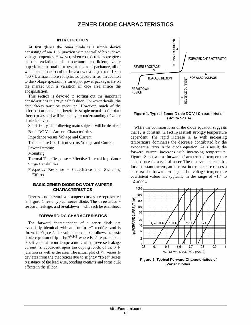
Reverse and forward volt-ampere curves are representedin Figure 1 for a typical zener diode. The three areas −forward, leakage, and breakdown − will each be examined.
FORWARD DC CHARACTERISTICS
The forward characteristics of a zener diode areessentially identical with an “ordinary” rectifier and isshown in Figure 2. The volt-ampere curve follows the basicdiode equation of IF = IReqV/KT where KT/q equals about0.026 volts at room temperature and IR (reverse leakagecurrent) is dependent upon the doping levels of the P-Njunction as well as the area. The actual plot of VF versus IFdeviates from the theoretical due to slightly “fixed” seriesresistance of the lead wire, bonding contacts and some bulkeffects in the silicon.
Figure 1. Typical Zener Diode DC V-I Characteristics(Not to Scale)
FORWARD VOLTAGE
REVERSE VOLTAGE
BREAKDOWNREGION
LEAKAGE REGION
FORWARD CHARACTERISTIC
FORW
ARD
CU
RR
ENT
REV
ERSE
CU
RR
ENT
While the common form of the diode equation suggeststhat IR is constant, in fact IR is itself strongly temperaturedependent. The rapid increase in IR with increasingtemperature dominates the decrease contributed by theexponential term in the diode equation. As a result, theforward current increases with increasing temperature.Figure 2 shows a forward characteristic temperaturedependence for a typical zener. These curves indicate thatfor a constant current, an increase in temperature causes adecrease in forward voltage. The voltage temperaturecoefficient values are typically in the range of −1.4 to−2 mV/°C.
Figure 2. Typical Forward Characteristics ofZener Diodes
10.90.80.70.60.50.40.3
1000
VF, FORWARD VOLTAGE (VOLTS)
500
200
100
50
20
10
5
2
1
I ,
FORW
ARD
CU
RR
ENT
(mA)
F
TJ = 150°C 100°C 25°C -55°C

http://onsemi.com19
LEAKAGE DC CHARACTERISTICS
When reverse voltage less than the breakdown is appliedto a zener diode, the behavior of current is similar to anyback-biased silicon P-N junction. Ideally, the reverse currentwould reach a level at about one volt reverse voltage andremain constant until breakdown is reached. There are boththeoretical and practical reasons why the typical V-I curvewill have a definite slope to it as seen in Figure 3.Multiplication effects and charge generation sites arepresent in a zener diode which dictate that reverse current(even at low voltages) will increase with voltage. Inaddition, surface charges are ever present across P-Njunctions which appear to be resistive in nature.
The leakage currents are generally less than onemicroampere at 150°C except with some large area devices.Quite often a leakage specification at 80% or so ofbreakdown voltage is used to assure low reverse currents.
Figure 3. Typical Leakage Currentversus Voltage
2016126400.1
1
10
100
1000
10000
I ,
REV
ERSE
LEA
KAG
E C
UR
REN
T (n
A)R
VR, REVERSE VOLTAGE (VOLTS)
TJ = 150°C
25°C
-55°C
VOLTAGE BREAKDOWN
At some definite reverse voltage, depending on the dopinglevels (resistivity) of the P-N junction, the current will beginto avalanche. This is the so-called “zener” or “breakdown”area and is where the device is usually biased during use. Atypical family of breakdown curves showing the effect oftemperature is illustrated in Figure 4.
Between the minimum currents shown in Figure 4 and theleakage currents, there is the “knee” region. The avalanchemechanism may not occur simultaneously across the entirearea of the P-N junction, but first at one microscopic site,then at an increasing number of sites as further voltage isapplied. This action can be accounted for by the“microplasma discharge” theory and correlates with severalbreakdown characteristics.
Figure 4. Typical Zener CharacteristicVariation with Temperature
32313029282726250.10.2
0.512
51020
50100200
5001000
VZ, ZENER VOLTAGE (VOLTS)
I ,
ZEN
ER C
UR
REN
T (m
A)Z
T = -�55°C 100°C25°C 150°C
T = TJT = TA
An exaggerated view of the knee region is shown inFigure 5. As can be seen, the breakdown or avalanchecurrent does not increase suddenly, but consists of a seriesof smoothly rising current versus voltage increments eachwith a sudden break point.
Figure 5. Exaggerated V-I Characteristicsof the Knee Region
EXAGGERATED V‐IOF KNEE REGION
ZENER VOLTAGE
VOLTAGE
ZEN
ER C
UR
REN
T CU
RR
ENT
At the lowest point, the zener resistance (slope of thecurve) would test high, but as current continues to climb, theresistance decreases. It is as though each discharge site hashigh resistance with each succeeding site being in paralleluntil the total resistance is very small.
In addition to the resistive effects, the micro plasmas mayact as noise generators. The exact process of manufacturingaffects how high the noise will be, but in any event there willbe some noise at the knee, and it will diminish considerablyas current is allowed to increase.
Since the zener impedance and the temperaturecoefficient are of prime importance when using the zenerdiode as a reference device, the next two sections willexpand on these points.
http://onsemi.com20
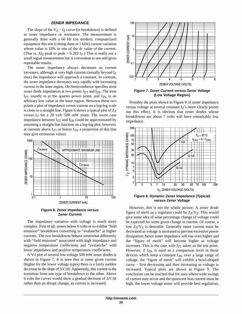
ZENER IMPEDANCE
The slope of the VZ − IZ curve (in breakdown) is definedas zener impedance or resistance. The measurement isgenerally done with a 60 Hz (on modern, computerizedequipment this test is being done at 1 kHz) current variationwhose value is 10% in rms of the dc value of the current.(That is, ΔIZ peak to peak = 0.282 IZ.) This is really not asmall signal measurement but is convenient to use and givesrepeatable results.
The zener impedance always decreases as currentincreases, although at very high currents (usually beyond IZmax) the impedance will approach a constant. In contrast,the zener impedance decreases very rapidly with increasingcurrent in the knee region. On Semiconductor specifies mostzener diode impedances at two points: IZT and IZK. The termIZT usually is at the quarter power point, and IZK is anarbitrary low value in the knee region. Between these twopoints a plot of impedance versus current on a log-log scaleis close to a straight line. Figure 6 shows a typical plot of ZZversus IZ for a 20 volt−500 mW zener. The worst caseimpedance between IZT and IZK could be approximated byassuming a straight line function on a log-log plot; however,at currents above IZT or below IZK a projection of this linemay give erroneous values.
Figure 6. Zener Impedance versusZener Current
ZENER CURRENT (mA)
1001010.11
10
100
1000
ZEN
ER IM
PED
ANC
E (O
HM
S) APPROXIMATE MAXIMUM LINE
ZZT(MAX)
ZZK(MAX)
The impedance variation with voltage is much morecomplex. First of all, zeners below 6 volts or so exhibit “fieldemission” breakdown converting to “avalanche” at highercurrents. The two breakdowns behave somewhat differentlywith “field emission” associated with high impedance andnegative temperature coefficients and “avalanche” withlower impedance and positive temperature coefficients.
A V-I plot of several low voltage 500 mW zener diodes isshown in Figure 7. It is seen that at some given current(higher for the lower voltage types) there is a fairly suddendecrease in the slope of ΔV/ΔI. Apparently, this current is thetransition from one type of breakdown to the other. Above6 volts the curves would show a gradual decrease of ΔV/ΔIrather than an abrupt change, as current is increased.
Figure 7. Zener Current versus Zener Voltage(Low Voltage Region)
1
100
10
1
0.1
0.012 3 4 5 6 7 8
ZENER VOLTAGE (VOLTS)
ZEN
ER C
UR
REN
T (m
A)
Possibly the plots shown in Figure 8 of zener impedanceversus voltage at several constant IZ’s more clearly pointsout this effect. It is obvious that zener diodes whosebreakdowns are about 7 volts will have remarkably lowimpedance.
20010070503020107532
1 mA
10 mA
20 mA
Figure 8. Dynamic Zener Impedance (Typical)versus Zener Voltage
2
3
57
10
20
30
5070
100
200Z
, D
YNAM
IC IM
PED
ANC
E (O
HM
S)Z
VZ, ZENER VOLTAGE (VOLTS)
TA = 25°CIZ(ac) = 0.1 IZ(dc)
However, this is not the whole picture. A zener diodefigure of merit as a regulator could be ZZ/VZ. This wouldgive some idea of what percentage change of voltage couldbe expected for some given change in current. Of course, alow ZZ/VZ is desirable. Generally zener current must bedecreased as voltage is increased to prevent excessive powerdissipation; hence zener impedance will rise even higher andthe “figure of merit” will become higher as voltageincreases. This is the case with IZT taken as the test point.However, if IZK is used as a comparison level in thosedevices which keep a constant IZK over a large range ofvoltage, the “figure of merit” will exhibit a bowl-shapedcurve − first decreasing and then increasing as voltage isincreased. Typical plots are shown in Figure 9. Theconclusion can be reached that for uses where wide swingsof current may occur and the quiescent bias current must behigh, the lower voltage zener will provide best regulation,
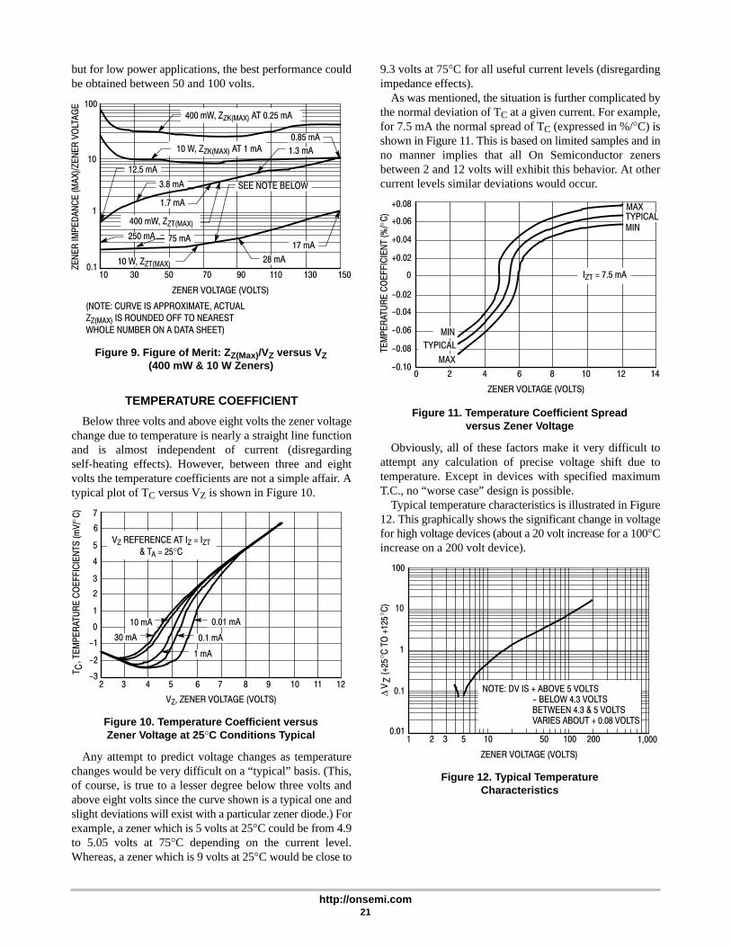
http://onsemi.com21
but for low power applications, the best performance couldbe obtained between 50 and 100 volts.
703010 50 90 110 130 150
0.85 mA
17 mA250 mA
10 W, ZZT(MAX)
1.7 mA
SEE NOTE BELOW
1.3 mA
12.5 mA
3.8 mA
28 mA
75 mA
ZENER VOLTAGE (VOLTS)
ZEN
ER IM
PED
ANC
E (M
AX)/Z
ENER
VO
LTAG
E
10
100
1
0.1
(NOTE: CURVE IS APPROXIMATE, ACTUALZZ(MAX) IS ROUNDED OFF TO NEARESTWHOLE NUMBER ON A DATA SHEET)
Figure 9. Figure of Merit: ZZ(Max)/VZ versus VZ(400 mW & 10 W Zeners)
400 mW, ZZK(MAX) AT 0.25 mA
10 W, ZZK(MAX) AT 1 mA
400 mW, ZZT(MAX)
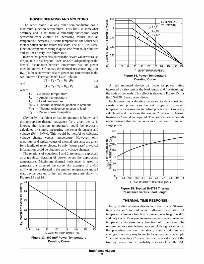
TEMPERATURE COEFFICIENT
Below three volts and above eight volts the zener voltagechange due to temperature is nearly a straight line functionand is almost independent of current (disregardingself-heating effects). However, between three and eightvolts the temperature coefficients are not a simple affair. Atypical plot of TC versus VZ is shown in Figure 10.
2 3 4 5 6 7 8 9 11
0.01 mA
0.1 mA30 mA
1 mA
10 mA
Figure 10. Temperature Coefficient versusZener Voltage at 25°C Conditions Typical
7
6
5
4
3
2
1
0
-1
-2
-3
VZ, ZENER VOLTAGE (VOLTS)
10 12
T ,
TEM
PER
ATU
RE
CO
EFFI
CIE
NTS
(mV/
�C)
C°
VZ REFERENCE AT IZ = IZT& TA = 25°C
Any attempt to predict voltage changes as temperaturechanges would be very difficult on a “typical” basis. (This,of course, is true to a lesser degree below three volts andabove eight volts since the curve shown is a typical one andslight deviations will exist with a particular zener diode.) Forexample, a zener which is 5 volts at 25°C could be from 4.9to 5.05 volts at 75°C depending on the current level.Whereas, a zener which is 9 volts at 25°C would be close to
9.3 volts at 75°C for all useful current levels (disregardingimpedance effects).
As was mentioned, the situation is further complicated bythe normal deviation of TC at a given current. For example,for 7.5 mA the normal spread of TC (expressed in %/°C) isshown in Figure 11. This is based on limited samples and inno manner implies that all On Semiconductor zenersbetween 2 and 12 volts will exhibit this behavior. At othercurrent levels similar deviations would occur.
+0.08
+0.06
+0.04
+0.02
0
-0.02
-0.08
-0.10
-0.04
-0.06
0 2 4 6 8 10 12 14
ZENER VOLTAGE (VOLTS)
TYPICAL
MAX
Figure 11. Temperature Coefficient Spreadversus Zener Voltage
TEM
PER
ATU
RE
CO
EFFI
CIE
NT
(%/�
C)
°
MAX
MIN
MIN
TYPICAL
IZT = 7.5 mA
Obviously, all of these factors make it very difficult toattempt any calculation of precise voltage shift due totemperature. Except in devices with specified maximumT.C., no “worse case” design is possible.
Typical temperature characteristics is illustrated in Figure12. This graphically shows the significant change in voltagefor high voltage devices (about a 20 volt increase for a 100°Cincrease on a 200 volt device).
NOTE: DV IS + ABOVE 5 VOLTS- BELOW 4.3 VOLTSBETWEEN 4.3 & 5 VOLTSVARIES ABOUT + 0.08 VOLTS
ZENER VOLTAGE (VOLTS)
1 2 3 5 10 50 100 200 1,000
100
10
1
0.1
Figure 12. Typical TemperatureCharacteristics
V
(+25
C T
O +
125
C)
°°
ΔZ
0.01
http://onsemi.com22
POWER DERATING AND MOUNTING
The zener diode like any other semiconductor has amaximum junction temperature. This limit is somewhatarbitrary and is set from a reliability viewpoint. Mostsemiconductors exhibit an increasing failure rate astemperature increases. At some temperature, the solder willmelt or soften and the failure rate soars. The 175°C to 200°Cjunction temperature rating is quite safe from solder failuresand still has a very low failure rate.
In order that power dissipated in the device will never causethe junction to rise beyond 175°C or 200°C (depending on thedevice), the relation between temperature rise and powermust be known. Of course, the thermal resistance (RθJA orRθJL) is the factor which relates power and temperature in thewell known “Thermal Ohm’s Law’’ relation:
ΔT = TJ − TA = RθJAPZ (1)and
ΔT = TJ − TL = RθJLPZ (2)where
TJTATLRθJARθJLPZ
= Junction temperature= Ambient temperature= Lead temperature= Thermal resistance junction to ambient= Thermal resistance junction to lead= Zener power dissipation
Obviously, if ambient or lead temperature is known andthe appropriate thermal resistance for a given device isknown, the junction temperature could be preciselycalculated by simply measuring the zener dc current andvoltage (PZ = IZVZ). This would be helpful to calculatevoltage change versus temperature. However, onlymaximum and typical values of thermal resistance are givenfor a family of zener diodes. So only “worst case” or typicalinformation could be obtained as to voltage changes.
The relations of equations 1 and 2 are usually expressedas a graphical derating of power versus the appropriatetemperature. Maximum thermal resistance is used togenerate the slope of the curve. An example of a 400milliwatt device derated to the ambient temperature and a 1watt device derated to the lead temperature are shown inFigures 13 and 14.
500
25 50 75 100 125 150 175 200
400
300
200
100
0
TA, AMBIENT TEMPERATURE (°C)
Figure 13. 400 mW Power TemperatureDerating Curve
P ,
PO
WER
DIS
SIPA
TIO
N (M
ILLI
WAT
TS)
D1.25
0 20 40 60 80 100 120 140 160 180 200
L = LEAD LENGTHTO HEAT SINK
1
0.75
0.50
0.25
L = 1/8″L = 3/8″
L = 1″
TL, LEAD TEMPERATURE (°C)
Figure 14. Power TemperatureDerating Curve
P ,
MAX
IMU
M P
OW
ER D
ISSI
PATI
ON
(WAT
TS)
D
A lead mounted device can have its power ratingincreased by shortening the lead length and “heatsinking”the ends of the leads. This effect is shown in Figure 15, forthe 1N4728, 1 watt zener diode.
Each zener has a derating curve on its data sheet andsteady state power can be set properly. However,temperature increases due to pulsed power are not so easilycalculated and therefore the use of “Transient ThermalResistance” would be required. The next section expoundsupon transient thermal behavior as a function of time andsurge power.
175
0
150
125
100
75
50
25
00.1 0.2 0.3 0.4 0.5 0.6 0.7 0.8 0.9 1
L, LEAD LENGTH TO HEAT SINK (INCH)
Figure 15. Typical 1N4728 ThermalResistance versus Lead Length
R�
JL, J
UN
CTI
ON
-TO
-LEA
DTH
ERM
AL R
ESIS
TAN
CE
(°C
/W)
THERMAL TIME RESPONSE
Early studies of zener diodes indicated that a “thermaltime constant” existed which allowed calculation oftemperature rise as a function of power pulse height, width,and duty cycle. More precise measurements have shown thattemperature response as a function of time cannot berepresented as a simple time constant. Although as shown inthe preceding section, the steady state conditions areanalogous in every way to an electrical resistance; a simple“thermal capacitance” placed across the resistor is not thetrue equivalent circuit. Probably a series of parallel R-C

http://onsemi.com23
networks or lumped constants representing a thermaltransmission line would be more accurate.
Fortunately a concept has developed in the industrywherein the exact thermal equivalent circuit need not befound. If one simply accepts the concept of a thermalresistance which varies with time in a predictable manner,the situation becomes very practical. For each family ofzener diodes, a “worst case” transient thermal resistancecurve may be generated.
The main use of this transient RθJL curve is when the zeneris used as a clipper or a protective device. First of all, thepower wave shape must be constructed. (Note, even thoughthe power-transient thermal resistance indicates reasonablejunction temperatures, the device still may fail if the peakcurrent exceeds certain values. Apparently a currentcrowding effect occurs which causes the zener to short. Thisis discussed further in this section.)
TRANSIENT POWER-TEMPERATURE EFFECTS
A typical transient thermal resistance curve is shown inFigure 16. This is for a lead mounted device and shows theeffect of lead length to an essentially infinite heatsink.
To calculate the temperature rise, the power surge waveshape must be approximated by its rectangular equivalent asshown in Figure 17. In case of an essentially non-recurrentpulse, there would be just one pulse, and ΔT = RθT1 Pp. Inthe general case, it can be shown that
whereDRθT1
RθT
RθT1 + T
RθJA(ss) or RθJL(ss) = Steady state value of thermalRθJA(ss) or RθJL(ss) = resistance
= Duty cycle in percent= Transient thermal resistance at the time
equal to the pulse width= Transient thermal resistance at the time
equal to pulse interval= Transient thermal resistance at the time
equal to the pulse interval= plus one more pulse width.
ΔT = [DRθJA (ss) + (1 − D) RθT1 + T + RθT1 − RθT] PP
PW, PULSE WIDTH (ms)
100
3 5 10 20 50 100 200 500 1000 2000 5000 10k 30k
7050
3020
10
75
32
1
L = 1/32″
L = 1″
FOR θJL(t) VALUES AT PULSE WIDTHSLESS THAN 3.0 ms, THE ABOVECURVE CAN BE EXTRAPOLATEDDOWN TO 10 μs AT A CONTINUINGSLOPE OF 1/2
Figure 16. Typical Transient ThermalResistance (For Axial Lead Zener)
L L
HEAT SINKÉÉÉÉ
ÉÉÉÉÉÉ
THER
MAL
RES
ISTA
NC
E (C
/W)
°R
JL(t)
, JU
NC
TIO
N‐T
O‐L
EAD
TR
ANSI
ENT
θ
Figure 17. Relation of Junction Temperature toPower Pulses
T
T1 T1T
PEAKTEMPERATURE RISE
AVERAGETEMPERATURE RISE
AMBIENTTEMPERATURE
PEAK POWER (PP)
AVERAGE POWER = PP
This method will predict the temperature rise at the end ofthe power pulse after the chain of pulses has reachedequilibrium. In other words, the average power will havecaused an average temperature rise which has stabilized, buta temperature “ripple” is present.
Example: (Use curve in Figure 16)PP = 5 watt (Lead length 1/32″)D = 0.1T1 = 10 msT = 100 msRθJA(ss) = 12°C/W (for 1/32″ lead length)
ThenRθT1 = 1.8°C/WRθT = 5.8°C/WRθT1 + T = 6°C/W
AndΔT = [0.1 x 12 + (1 − 0.1) 6 + 1.8 − 5.8] 5ΔT = 13°C
Or at TA = 25°, TJ = 38°C peak
SURGE FAILURES
If no other considerations were present, it would be asimple matter to specify a maximum junction temperatureno matter what pulses are present. However, as has beennoted, apparently other fault conditions prevail. The samegroup of devices for which the transient thermal curves weregenerated were tested by subjecting them to single shotpower pulses. A failure was defined as a significant shift ofleakage or zener voltage, or of course opens or shorts. Eachdevice was measured before and after the applied pulse.Most failures were shifts in zener voltage. The results areshown in Figure 18.
Attempts to correlate this to the transient thermalresistance work quite well on a typical basis. For example,assuming a value for 1 ms of 90 watts and 35 watts at 10 ms,the predicted temperature rise would be 180°C and 190°C.But on a worst case basis, the temperature rises would beabout one half these values or junction temperatures, on theorder of 85°C to 105°C, which are obviously low.Apparently at very high power levels a current restrictionoccurs causing hot spots. There was no apparent correlation
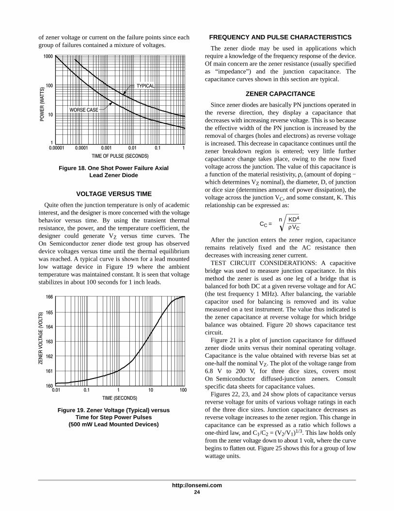
http://onsemi.com24
of zener voltage or current on the failure points since eachgroup of failures contained a mixture of voltages.
1000
0.00001 0.0001 0.001 0.01 0.1 1
WORSE CASE
100
10
1
POW
ER (W
ATTS
)
Figure 18. One Shot Power Failure AxialLead Zener Diode
TIME OF PULSE (SECONDS)
TYPICAL
VOLTAGE VERSUS TIME
Quite often the junction temperature is only of academicinterest, and the designer is more concerned with the voltagebehavior versus time. By using the transient thermalresistance, the power, and the temperature coefficient, thedesigner could generate VZ versus time curves. TheOn Semiconductor zener diode test group has observeddevice voltages versus time until the thermal equilibriumwas reached. A typical curve is shown for a lead mountedlow wattage device in Figure 19 where the ambienttemperature was maintained constant. It is seen that voltagestabilizes in about 100 seconds for 1 inch leads.
166
0.01
165
164
163
162
161
1600.1 1 10 100
TIME (SECONDS)
ZEN
ER V
OLT
AGE
(VO
LTS)
Figure 19. Zener Voltage (Typical) versusTime for Step Power Pulses
(500 mW Lead Mounted Devices)
FREQUENCY AND PULSE CHARACTERISTICS
The zener diode may be used in applications whichrequire a knowledge of the frequency response of the device.Of main concern are the zener resistance (usually specifiedas “impedance”) and the junction capacitance. Thecapacitance curves shown in this section are typical.
ZENER CAPACITANCE
Since zener diodes are basically PN junctions operated inthe reverse direction, they display a capacitance thatdecreases with increasing reverse voltage. This is so becausethe effective width of the PN junction is increased by theremoval of charges (holes and electrons) as reverse voltageis increased. This decrease in capacitance continues until thezener breakdown region is entered; very little furthercapacitance change takes place, owing to the now fixedvoltage across the junction. The value of this capacitance isa function of the material resistivity, ρ, (amount of doping −which determines VZ nominal), the diameter, D, of junctionor dice size (determines amount of power dissipation), thevoltage across the junction VC, and some constant, K. Thisrelationship can be expressed as:
KD4pVC
�CC =n KD4
ρVC
After the junction enters the zener region, capacitanceremains relatively fixed and the AC resistance thendecreases with increasing zener current.
TEST CIRCUIT CONSIDERATIONS: A capacitivebridge was used to measure junction capacitance. In thismethod the zener is used as one leg of a bridge that isbalanced for both DC at a given reverse voltage and for AC(the test frequency 1 MHz). After balancing, the variablecapacitor used for balancing is removed and its valuemeasured on a test instrument. The value thus indicated isthe zener capacitance at reverse voltage for which bridgebalance was obtained. Figure 20 shows capacitance testcircuit.
Figure 21 is a plot of junction capacitance for diffusedzener diode units versus their nominal operating voltage.Capacitance is the value obtained with reverse bias set atone-half the nominal VZ. The plot of the voltage range from6.8 V to 200 V, for three dice sizes, covers mostOn Semiconductor diffused-junction zeners. Consultspecific data sheets for capacitance values.
Figures 22, 23, and 24 show plots of capacitance versusreverse voltage for units of various voltage ratings in eachof the three dice sizes. Junction capacitance decreases asreverse voltage increases to the zener region. This change incapacitance can be expressed as a ratio which follows aone-third law, and C1/C2 = (V2/V1)1/3. This law holds onlyfrom the zener voltage down to about 1 volt, where the curvebegins to flatten out. Figure 25 shows this for a group of lowwattage units.

http://onsemi.com25
Figure 20. Capacitance Test Circuit
C1
C2
VDC1 k1% 1 k
1%1 k1%
1 k1%
DCPOWERSUPPLY
100 W
IV
VAC
1 MHz
SIGNALGEN
10/50pF
XZENERUNDERTEST
HI‐GAINDIFF SCOPE
R = ZR R
CAPDECADE0-.09 mF100 pFSTEPSΔC 1%
BAL READ
S1
10/150pF
L/CMETER
0.1 μF
1,000
1 10 100
VR, REVERSE VOLTAGE (VOLTS)
100
10
C
, CAP
ACIT
ANC
E (P
ICO
FAR
ADS)
Z
100 VOLTS
50 VOLTS
20 VOLTS
10 VOLTS
10,000
1 10 100 1,000
1,000
100
10C
, CAP
ACIT
ANC
E (P
ICO
FAR
ADS)
@ V
Z/2
VZ, NOMINAL UNIT VOLTAGE (VOLTS)
Z
HIGH WATTAGE
LOW WATTAGE
MEDIUM WATTAGE
Figure 21. Capacitance versus Voltage Figure 22. Capacitance versus Reverse Voltage
LOW WATTAGE UNITSAVG. FOR 10 UNITS EACH
10,000
1 10
VR, REVERSE VOLTAGE (VOLTS)
100
C
, CAP
ACIT
ANC
E (P
ICO
FAR
ADS)
Z
100
1,000
10,000
1 10 1,000
VR, REVERSE VOLTAGE (VOLTS)
100
10
C
, CAP
ACIT
ANC
E (P
ICO
FAR
ADS)
Z
100
1,000
Figure 23. Capacitance versusReverse Voltage
Figure 24. Capacitance versusReverse Voltage
100 VOLTS
50 VOLTS
20 VOLTS
10 VOLTS
100 VOLTS
50 VOLTS
20 VOLTS
10 VOLTSMEDIUM WATTAGE UNITSAVG. FOR 10 UNITS EACH
HIGH WATTAGE UNITSAVG. FOR 10 UNITS EACH
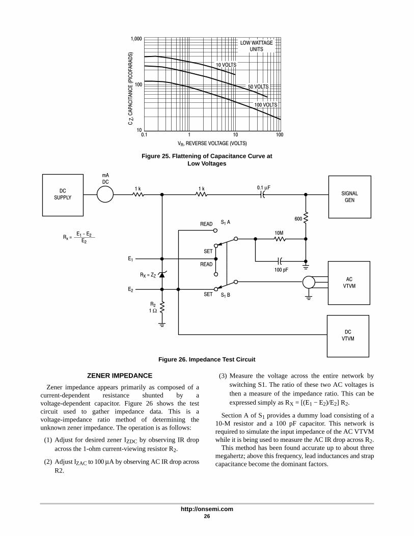
http://onsemi.com26
C
, CAP
ACIT
ANC
E (P
ICO
FAR
ADS)
Z
100
1,000
101 10
VR, REVERSE VOLTAGE (VOLTS)
1000.1
LOW WATTAGEUNITS
Figure 25. Flattening of Capacitance Curve atLow Voltages
100 VOLTS
50 VOLTS
10 VOLTS
Figure 26. Impedance Test Circuit
1 k 1 k
R21 Ω
RX = ZZ
DCSUPPLY
mADC
E1
E2
Rx =E1 - E2
E2
0.1 μF
600READ S1 A
READ
SET
SET
10M
100 pF
S1 B
SIGNALGEN
ACVTVM
DCVTVM
ZENER IMPEDANCE
Zener impedance appears primarily as composed of acurrent-dependent resistance shunted by avoltage-dependent capacitor. Figure 26 shows the testcircuit used to gather impedance data. This is avoltage-impedance ratio method of determining theunknown zener impedance. The operation is as follows:
(1) Adjust for desired zener IZDC by observing IR dropacross the 1-ohm current-viewing resistor R2.
(2) Adjust IZAC to 100 μA by observing AC IR drop acrossR2.
(3) Measure the voltage across the entire network byswitching S1. The ratio of these two AC voltages isthen a measure of the impedance ratio. This can beexpressed simply as RX = [(E1 − E2)/E2] R2.
Section A of S1 provides a dummy load consisting of a10-M resistor and a 100 pF capacitor. This network isrequired to simulate the input impedance of the AC VTVMwhile it is being used to measure the AC IR drop across R2.
This method has been found accurate up to about threemegahertz; above this frequency, lead inductances and strapcapacitance become the dominant factors.

http://onsemi.com27
Figure 27 shows typical impedance versus frequencyrelationships of 6.8 volt 500 mW zener diodes at various DCzener currents. Before the zener breakdown region isentered, the impedance is almost all reactive, being providedby a voltage-dependent capacitor shunted by a very highresistance. When the zener breakdown region is entered, thecapacitance is fixed and now is shunted bycurrent-dependent resistance. For comparison, Figure 27also shows the plot for a 680 pF capacitor XC, a 1K 1%nonreactive resistor, R, and the parallel combination of thesetwo passive elements, ZT.
ZTIZMA
2
1020
1K & 680 pF
R, 1K 1% DC
10,000
10 100 1 kHz 10 kHz 100 kHz 1 MHz 10 MHz
FREQUENCY (Hz)
1,000
100
10
1
Z ,
ZEN
ER IM
PED
ANC
E (O
HM
S)Z
X , 680 pFC
Figure 27. Zener Impedanceversus Frequency
1.00
2.50
5
0.25
0.50
HIGH FREQUENCY AND SWITCHINGCONSIDERATIONS
At frequencies about 100 kHz or so and switching speedsabove 10 microseconds, shunt capacitance of zener diodesbegins to seriously effect their usefulness. The upper photoof Figure 28 shows the output waveform of a symmetricalpeak limiter using two zener diodes back-to-back. Thecapacitive effects are obvious here. In any application wherethe signal is recurrent, the shunt capacitance limitations canbe overcome, as lower photo of Figure 28 shows. This isdone by operating fast diodes in series with the zener. Uponapplication of a signal, the fast diode conducts in the forwarddirection charging the shunt zener capacitance to the levelwhere the zener conducts and limits the peak. When thesignal swings the opposite direction, the fast diode becomesback-biased and prevents fast discharge of shuntcapacitance. The fast diode remains back-biased when thesignal reverses again to the forward direction and remainsoff until the input signal rises and exceeds the charge levelof the capacitor. When the signal exceeds this level, the fastdiode conducts as does the zener. Thus, between successivecycles or pulses the charge in the shunt capacitor holds offthe fast diode, preventing capacitive loading of the signaluntil zener breakdown is reached. Figures 29 and 30 showthis method applied to fast-pulse peak limiting.
5 V/cm
0.5 μs/cm
0.5 μs/cm
5 V/cm
Figure 28. Symmetrical Peak Limiter
RS
RS
ei eo
ei eo

http://onsemi.com28
2 V/cm
20 ns/cm
ei
eo
2 V/cm
eo
ei
20 ns/cm
Figure 29. Shunt Clipper
Figure 30. Shunt Clipper with Clamping Network
200 Ω
50 Ωei eo10 V
Z
200 Ω
50 Ωei
0.001
eo

http://onsemi.com29
Figure 31 is a photo of input-output pulse waveformsusing a zener alone as a series peak clipper. The smalleroutput waveform shows the capacitive spike on the leading
edge. Figure 32 clearly points out the advantage of theclamping network.
2 V/cm
20 ns/cm
eo
ei
2 V/cmeo
ei
20 ns/cm
0
Figure 31. Basic Series Clipper
Figure 32. Series Clipper with Clamping Network
10 VZ
50 Ω
50 Ω
ei eo
ei eo
200 Ω
10 VZ
200 Ω
.001
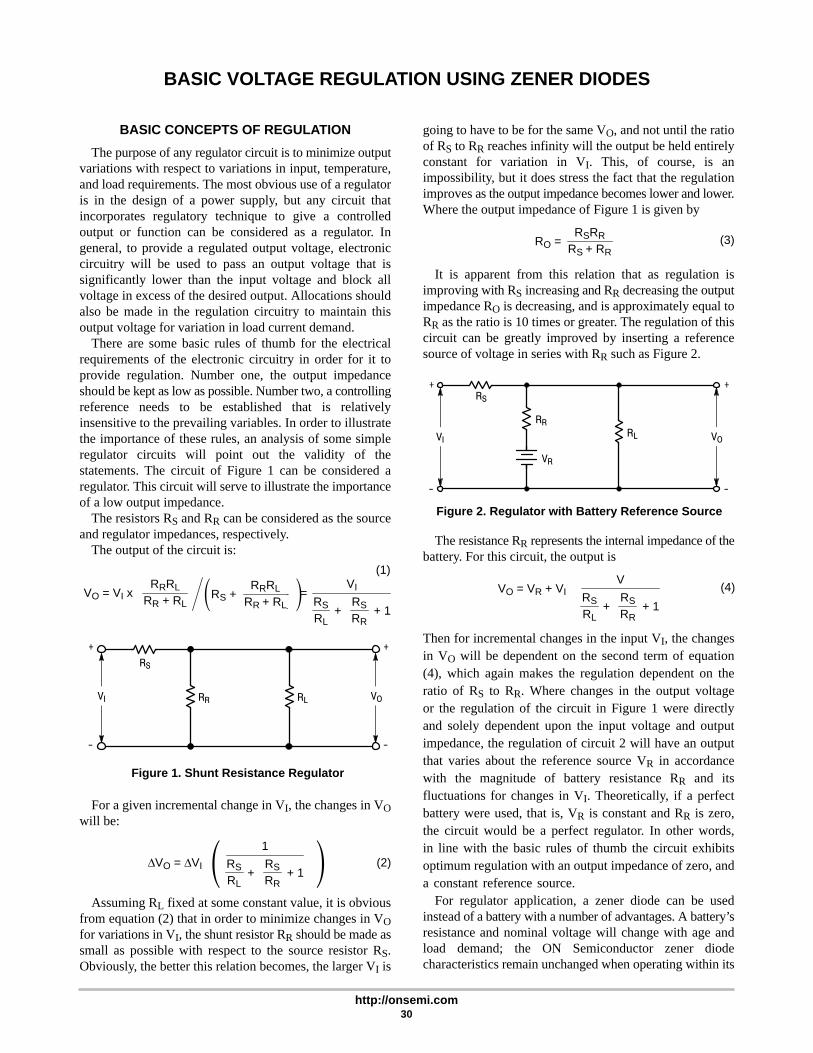
http://onsemi.com30
BASIC VOLTAGE REGULATION USING ZENER DIODES
BASIC CONCEPTS OF REGULATION
The purpose of any regulator circuit is to minimize outputvariations with respect to variations in input, temperature,and load requirements. The most obvious use of a regulatoris in the design of a power supply, but any circuit thatincorporates regulatory technique to give a controlledoutput or function can be considered as a regulator. Ingeneral, to provide a regulated output voltage, electroniccircuitry will be used to pass an output voltage that issignificantly lower than the input voltage and block allvoltage in excess of the desired output. Allocations shouldalso be made in the regulation circuitry to maintain thisoutput voltage for variation in load current demand.
There are some basic rules of thumb for the electricalrequirements of the electronic circuitry in order for it toprovide regulation. Number one, the output impedanceshould be kept as low as possible. Number two, a controllingreference needs to be established that is relativelyinsensitive to the prevailing variables. In order to illustratethe importance of these rules, an analysis of some simpleregulator circuits will point out the validity of thestatements. The circuit of Figure 1 can be considered aregulator. This circuit will serve to illustrate the importanceof a low output impedance.
The resistors RS and RR can be considered as the sourceand regulator impedances, respectively.
The output of the circuit is:
�RS
RRRL
RR � RL�
(1)
VO = VI xRRRL
RR + RLRS +
RRRL
RR + RL=
VI
RS
RL
RS
RR+ + 1
Figure 1. Shunt Resistance Regulator
+
-
RS
RR RL
+
-
VI VO
For a given incremental change in VI, the changes in VOwill be:
(2)�RRRRL
RR ��ΔVO = ΔVI
1
RS
RL
RS
RR+ + 1
Assuming RL fixed at some constant value, it is obviousfrom equation (2) that in order to minimize changes in VOfor variations in VI, the shunt resistor RR should be made assmall as possible with respect to the source resistor RS.Obviously, the better this relation becomes, the larger VI is
going to have to be for the same VO, and not until the ratioof RS to RR reaches infinity will the output be held entirelyconstant for variation in VI. This, of course, is animpossibility, but it does stress the fact that the regulationimproves as the output impedance becomes lower and lower.Where the output impedance of Figure 1 is given by
(3)RO =RSRR
RS + RR
It is apparent from this relation that as regulation isimproving with RS increasing and RR decreasing the outputimpedance RO is decreasing, and is approximately equal toRR as the ratio is 10 times or greater. The regulation of thiscircuit can be greatly improved by inserting a referencesource of voltage in series with RR such as Figure 2.
Figure 2. Regulator with Battery Reference Source
+
-
RS
VR
RL
RR
+
-
VI VO
The resistance RR represents the internal impedance of thebattery. For this circuit, the output is
(4)VO = VR + VIV
RS
RL
RS
RR+ + 1
Then for incremental changes in the input VI, the changesin VO will be dependent on the second term of equation(4), which again makes the regulation dependent on theratio of RS to RR. Where changes in the output voltageor the regulation of the circuit in Figure 1 were directlyand solely dependent upon the input voltage and outputimpedance, the regulation of circuit 2 will have an outputthat varies about the reference source VR in accordancewith the magnitude of battery resistance RR and itsfluctuations for changes in VI. Theoretically, if a perfectbattery were used, that is, VR is constant and RR is zero,the circuit would be a perfect regulator. In other words,in line with the basic rules of thumb the circuit exhibitsoptimum regulation with an output impedance of zero, anda constant reference source.
For regulator application, a zener diode can be usedinstead of a battery with a number of advantages. A battery’sresistance and nominal voltage will change with age andload demand; the ON Semiconductor zener diodecharacteristics remain unchanged when operating within its
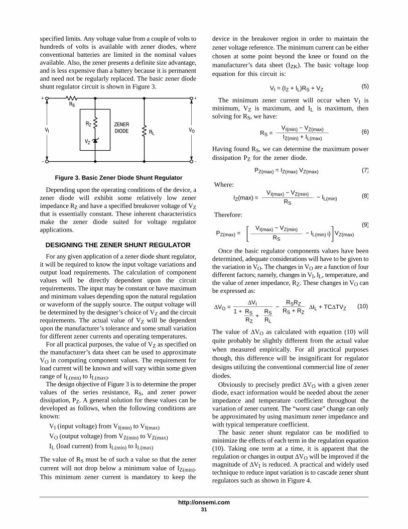
http://onsemi.com31
specified limits. Any voltage value from a couple of volts tohundreds of volts is available with zener diodes, whereconventional batteries are limited in the nominal valuesavailable. Also, the zener presents a definite size advantage,and is less expensive than a battery because it is permanentand need not be regularly replaced. The basic zener diodeshunt regulator circuit is shown in Figure 3.
Figure 3. Basic Zener Diode Shunt Regulator
+
-
RS
RL
RZ
VZ
ZENERDIODE
+
-
VI VO
Depending upon the operating conditions of the device, azener diode will exhibit some relatively low zenerimpedance RZ and have a specified breakover voltage of VZthat is essentially constant. These inherent characteristicsmake the zener diode suited for voltage regulatorapplications.
DESIGNING THE ZENER SHUNT REGULATOR
For any given application of a zener diode shunt regulator,it will be required to know the input voltage variations andoutput load requirements. The calculation of componentvalues will be directly dependent upon the circuitrequirements. The input may be constant or have maximumand minimum values depending upon the natural regulationor waveform of the supply source. The output voltage willbe determined by the designer’s choice of VZ and the circuitrequirements. The actual value of VZ will be dependentupon the manufacturer’s tolerance and some small variationfor different zener currents and operating temperatures.
For all practical purposes, the value of VZ as specified onthe manufacturer’s data sheet can be used to approximateVO in computing component values. The requirement forload current will be known and will vary within some givenrange of IL(min) to IL(max).
The design objective of Figure 3 is to determine the propervalues of the series resistance, RS, and zener powerdissipation, PZ. A general solution for these values can bedeveloped as follows, when the following conditions areknown:
VI (input voltage) from VI(min) to VI(max)
VO (output voltage) from VZ(min) to VZ(max)
IL (load current) from IL(min) to IL(max)
The value of RS must be of such a value so that the zenercurrent will not drop below a minimum value of IZ(min).This minimum zener current is mandatory to keep the
device in the breakover region in order to maintain thezener voltage reference. The minimum current can be eitherchosen at some point beyond the knee or found on themanufacturer’s data sheet (IZK). The basic voltage loopequation for this circuit is:
(5)VI = (IZ + IL)RS + VZ
The minimum zener current will occur when VI isminimum, VZ is maximum, and IL is maximum, thensolving for RS, we have:
(6)VI(min) − VZ(max)
IZ(min) + IL(max)RS =
Having found RS, we can determine the maximum powerdissipation PZ for the zener diode.
PZ(max) = VZ(max)�VI(max) � VZ(min)RS
� IL(min)�
(7)
(8)
(9)
PZ(max) = IZ(max) VZ(max)
Where:
IZ(max) =VI(max) − VZ(min)
RS− IL(min)
Therefore:
VI(max) − VZ(min)
RS− IL(min)
Once the basic regulator components values have beendetermined, adequate considerations will have to be given tothe variation in VO. The changes in VO are a function of fourdifferent factors; namely, changes in VI, IL, temperature, andthe value of zener impedance, RZ. These changes in VO canbe expressed as:
(10)RSRZ
RS + RZ
ΔVI
RS
RZ
RS
RL+
1 +ΔVO = − ΔIL + TCΔTVZ
The value of ΔVO as calculated with equation (10) willquite probably be slightly different from the actual valuewhen measured empirically. For all practical purposesthough, this difference will be insignificant for regulatordesigns utilizing the conventional commercial line of zenerdiodes.
Obviously to precisely predict ΔVO with a given zenerdiode, exact information would be needed about the zenerimpedance and temperature coefficient throughout thevariation of zener current. The “worst case” change can onlybe approximated by using maximum zener impedance andwith typical temperature coefficient.
The basic zener shunt regulator can be modified tominimize the effects of each term in the regulation equation(10). Taking one term at a time, it is apparent that theregulation or changes in output ΔVO will be improved if themagnitude of ΔVI is reduced. A practical and widely usedtechnique to reduce input variation is to cascade zener shuntregulators such as shown in Figure 4.

http://onsemi.com32
Figure 4. Cascaded Zener Shunt Regulators ReduceΔVO by Reducing ΔVI to the Succeeding Stages
-
+RS2
Z1 RL
RS1
-
Z2RL′
+
VI VOVO′ = VI′ = VZ1
This, in essence, is a regulator driven with a pre-regulatorso that the over all regulation is the product of both. Theregulation or changes in output voltage is determined by:
Where:
RL′ = RS2 +RLRZ2
RL + RZ2and IL′ = IL + IZ2
(11)
RS2RZ2
RS2 + RZ2
ΔVZI
RS2
RL+1 +
ΔVO = −
ΔIL + TC2 ΔTVZ2
RS2
RZ2
(12)
RS1RZ1
RS1 + RZ1
ΔVI
RS1
RL′ +1 +
ΔVZ1 = ΔVO′ = −
ΔIL′ + TC1 ΔTVZ1
RS1
RZ1
The changes in output with respect to changes in input forboth stages assuming the temperature and load are constantis
(13)ΔVOΔVZ1
ΔVOΔVO′= = Regulation of second stage
(14)
(15)
= Regulation of first stage
ΔVO′ΔVI
= Combined regulationxΔVOΔVO′=
ΔVOΔVI
ΔVO′ΔVI
Obviously, this technique will vastly improve overallregulation where the input fluctuates over a relatively widerange. As an example, let’s say the input varies by ±20% andthe regulation of each individual stage reduces the variationby a factor of 1/20. This then gives an overall outputvariation of ±20% × (1/20)2 or ±0.05%.
The next two factors in equation (10) affecting regulationare changes in load current and temperature excursions. Inorder to minimize changes for load current variation, theoutput impedance RZRS/(RZ + RS) will have to be reduced.This can only be done by having a lower zener impedancebecause the value of RS is fixed by circuit requirements.There are basically two ways that a lower zener impedancecan be achieved. One, a higher wattage device can be usedwhich allows for an increase in zener current of which willreduce the impedance. The other technique is to series lowervoltage devices to obtain the desired equivalent voltage, sothat the sum of the impedance is less than that for a single
high voltage device. So to speak, this technique will kill twobirds with one stone, as it can also be used to minimizetemperature induced variations of the regulator.
In most regulator applications, the single most detrimentalfactor affecting regulation is that of variation in junctiontemperature. The junction temperature is a function of boththe ambient temperature and that of self heating. In order toillustrate how the overall temperature coefficient isimproved with series lower voltage zener, a mathematicalrelationship can be developed. Consider the diagram ofFigure 5.
Figure 5. Series Zener Improve Dynamic Impedanceand Temperature Coefficient
+
-
RS
RL
Z1
Z2
Zn
+
-
VI VO
With the temperature coefficient TC defined as the % changeper °C, the change in output for a given temperature rangewill equal some overall TC x ΔT x Total VZ. Such as
(16)ΔVO(ΔT) = TC ΔT (VZ1 + VZ2 + . . . + VZN)
Obviously, the change in output will also be equal to thesum of the changes as attributed from each zener.
(17)ΔVO(ΔT) = ΔT(TC1VZ1 + TC2VZ2 + . . . + TCNVZN)
Setting the two equations equal to each other and solvingfor the overall TC, we get
(18)
(19)
TCΔT(VZ1 + VZ2 + . . . + VZN) = ΔT(TC1VZ1+ TC2VZ2 + . . . + TCNVZN)
TC =TC1 VZ1 + TC2VZ2 + . . . + TCNVZN
VZ1 + VZ2 + . . . + VZN
For equation (19) the overall temperature coefficient forany combination of series zeners can be calculated. Say forinstance several identical zeners in series replace a singlehigher voltage zener. The new overall temperaturecoefficient will now be that of one of the low voltagedevices. This allows the designer to go to the manufacturer’s

http://onsemi.com33
data sheet and select a combination of low TC zener diodesin place of the single higher TC devices. Generally speaking,the technique of using multiple devices will also yield alower dynamic impedance. Advantages of this technique arebest demonstrated by example. Consider a 5 watt diode witha nominal zener voltage of 10 volts exhibits approximately0.055% change in voltage per degree centrigrade, a 20 voltunit approximately 0.075%/°C, and a 100 volt unitapproximately 0.1%/°C. In the case of the 100 volt diode,five 20 volt diodes could be connected together to providethe correct voltage reference, but the overall temperaturecoefficient would remain that of the low voltage units, i.e.0.075%/°C. It should also be noted that the same seriescombination improves the overall zener impedance inaddition to the temperature coefficient. A 20 volt, 5 wattON Semiconductor zener diode has a maximum zenerimpedance of 3 ohms, compared to the 90 ohms impedancewhich is maximum for a 100 volt unit. Although theseimpedances are measured at different current levels, theseries impedance of five 20 volt zener diodes is still muchlower than that of a single 100 volt zener diode at the testcurrent specified on the data sheet.
For the ultimate in zener shunt regulator performance, theaforementioned techniques can be combined with the properselection of devices to yield an overall improvement inregulation. For instance, a multiple string of low voltagezener diodes can be used as a preregulator, with a seriescombination of zero TC reference diodes in the final stagesuch as Figure 6.
The first stage will reduce the large variation in VI to somerelatively low level, i.e. ΔVZ. This ΔVZ is optimized byutilizing a series combination of zeners to reduce the overallTC and ΔVZ. Because of this small fluctuation of input to thesecond stage, and if RL is constant, the biasing current of theTC units can be maintained at their specified level. This willgive an output that is very precise and not significantlyaffected by changes in input voltage or junction temperature.
Figure 6. Series Zeners Cascaded With SeriesReference Diodes for Improved Zener
Shunt Regulation
RS1 RS2
Z1
Z2
Z3
Z4
RL
TC1
TC2
+
-
+
-
VI VO
The basic zener shunt regulator exhibits some inherentlimitations to the designer. First of all, the zener is limited toits particular power dissipating rating which may be lessthan the required amount for a particular situation. The totalmagnitude of dissipation can be increased to some degree byutilizing series or parallel units. Zeners in series present few
problems because individual voltages are additive and thedevices all carry the same current and the extent that thistechnique can be used is only restricted by the feasibility ofcircuit parameters and cost. On the other hand, caution mustbe taken when attempting to parallel zener diodes. If thedevices are not closely matched so that they all break overat the same voltage, the low voltage device will go intoconduction first and ultimately carry all the current. In orderto avoid this situation, the diodes should be matched forequal current sharing.
EXTENDING POWER AND CURRENT RANGE
The most common practice for extending the powerhandling capabilities of a regulator is to incorporatetransistors in the design. This technique is discussed in detailin the following sections of this section. The seconddisadvantage to the basic zener shunt regulator is thatbecause the device does not have a gain function, a feedbacksystem is not possible with just the zener resistorcombination. For very precise regulators, the design willnormally be an electronic circuit consisting of transistordevices for control, probably a closed loop feedback systemwith a zener device as the basic referencing element.
The concept of regulation can be further extended andimproved with the addition of transistors as the powerabsorbing elements to the zener diodes establishing areference. There are three basic techniques used thatcombine zener diodes and transistors for voltage regulation.The shunt transistor type shown in Figure 7 will extend thepower handling capabilities of the basic shunt regulator, andexhibit marked improvement in regulation.
Figure 7. Basic Transistor Shunt Regulator
RL
RS
ZIZIC
RB
IB
VBE
Q1 IL
-
+
-
+
VI VO
In this configuration the source resistance must be largeenough to absorb the overvoltage in the same manner as inthe conventional zener shunt regulator. Most of the shuntregulating current in this circuit will pass through thetransistor reducing the current requirements of the zenerdiode by essentially the dc current gain of the transistor hFE.Where the total regulating shunt current is:
(20)
IS = IZ + IC = IZ + IB hFE
where
therefore
IZ = IB + IRB and IB >> IRB
IS ≈ IZ + IZ hFE = IZ (1 + hFE)
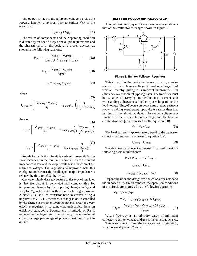
http://onsemi.com34
The output voltage is the reference voltage VZ plus theforward junction drop from base to emitter VBE of thetransistor.
(21)VO = VZ + VBE
The values of components and their operating conditionis dictated by the specific input and output requirements andthe characteristics of the designer’s chosen devices, asshown in the following relations:
(22)RS =VI(min) − VO(max)
IZ(min) [1+hFE(min)] + IL(max)
RB =VI(min) − VZ(max)
IZ(min)
PDZ = IZ(max) VZ(max)
when
IZ(max) = �VI(max) � V O(min)
RS� IL(min) �� 1
1 � hFE(min)�
hence
VI(max) − VO(min)
RS− IL(min)
11 + hFE(min)
PDZ = �VI(max) � VO(min)
RS� IL(min) �� 1
1 � hFE(min)�VI(max) − VO(min)
RS− IL(min)
VZ(max)
1 + hFE(min)
PDQ = �VI(max) � V O(min)
RS� IL(min) ��1 888888 �VI(max) − VO(min)
RS− IL(min) VO(max)
(23)
(24)
(25)
(26)
(27)
Regulation with this circuit is derived in essentially thesame manner as in the shunt zener circuit, where the outputimpedance is low and the output voltage is a function of thereference voltage. The regulation is improved with thisconfiguration because the small signal output impedance isreduced by the gain of Q1 by 1/hFE.
One other highly desirable feature of this type of regulatoris that the output is somewhat self compensating fortemperature changes by the opposing changes in VZ andVBE for VZ ≈ 10 volts. With the zener having a positive2 mV/°C TC and the transistor base to emitter being anegative 2 mV/°C TC, therefore, a change in one is cancelledby the change in the other. Even though this circuit is a veryeffective regulator it is somewhat undesirable from anefficiency standpoint. Because the magnitude of RS isrequired to be large, and it must carry the entire inputcurrent, a large percentage of power is lost from input tooutput.
EMITTER FOLLOWER REGULATOR
Another basic technique of transistor-zener regulation isthat of the emitter follower type shown in Figure 8.
Figure 8. Emitter Follower Regulator
RS
RB
Z1
IRB
IZ
+
- VBE
-
+
ILRL
Q1IC
+
-
+
-
VI VO
This circuit has the desirable feature of using a seriestransistor to absorb overvoltages instead of a large fixedresistor, thereby giving a significant improvement inefficiency over the shunt type regulator. The transistor mustbe capable of carrying the entire load current andwithstanding voltages equal to the input voltage minus theload voltage. This, of course, imposes a much more stringentpower handling requirement upon the transistor than wasrequired in the shunt regulator. The output voltage is afunction of the zener reference voltage and the base toemitter drop of Q1 as expressed by the equation (28).
(28)VO = VZ − VBE
The load current is approximately equal to the transistorcollector current, such as shown in equation (29).
(29)IL(max) ≈ IC(max)
The designer must select a transistor that will meet thefollowing basic requirements:
(30)
PD ≅ (VI(max) − VO)IL(max)
IC(max) ≈ IL(max)
BVCES ≥ (VI(max) − VO)
Depending upon the designer’s choice of a transistor andthe imposed circuit requirements, the operation conditionsof the circuit are expressed by the following equations:
(31)
VZ = VO + VBE
= VO + IL(max)/gFE(min) @ IL(max)
RS =VI(min) − VZ − VCE(min) @ IL(max)
IL(max)
Where VCE(min) is an arbitrary value of minimumcollector to emitter voltage and gFE is the transconductance.
This is sufficient to keep the transistor out of saturation,which is usually about 2 volts.
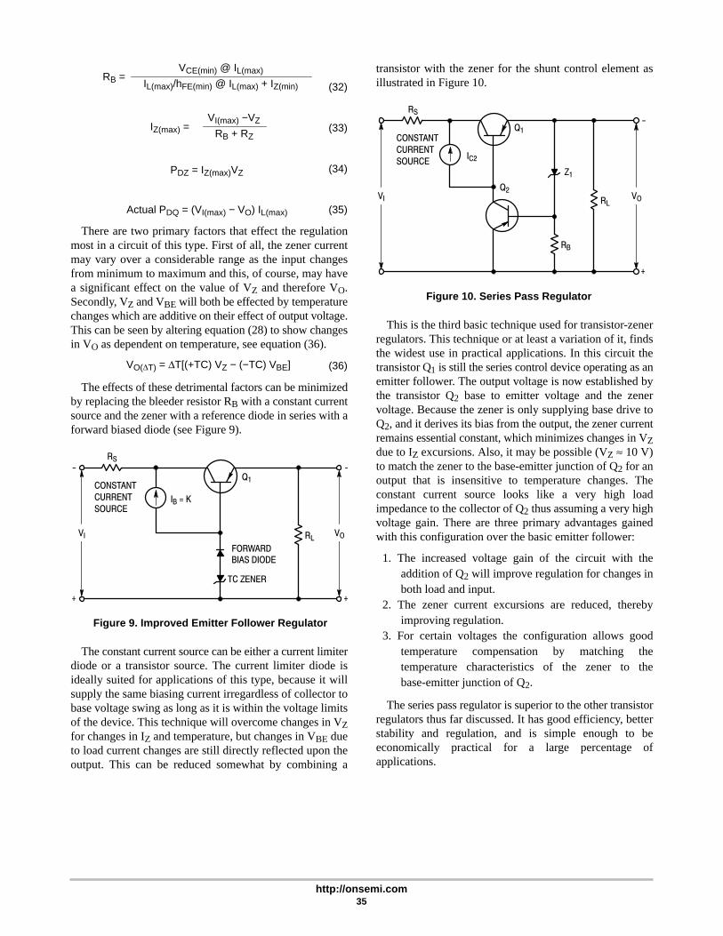
http://onsemi.com35
(32)RB =
VCE(min) @ IL(max)
IL(max)/hFE(min) @ IL(max) + IZ(min)
IZ(max) =VI(max) −VZ
RB + RZ
PDZ = IZ(max)VZ
Actual PDQ = (VI(max) − VO) IL(max)
(33)
(34)
(35)
There are two primary factors that effect the regulationmost in a circuit of this type. First of all, the zener currentmay vary over a considerable range as the input changesfrom minimum to maximum and this, of course, may havea significant effect on the value of VZ and therefore VO.Secondly, VZ and VBE will both be effected by temperaturechanges which are additive on their effect of output voltage.This can be seen by altering equation (28) to show changesin VO as dependent on temperature, see equation (36).
(36)VO(ΔT) = ΔT[(+TC) VZ − (−TC) VBE]
The effects of these detrimental factors can be minimizedby replacing the bleeder resistor RB with a constant currentsource and the zener with a reference diode in series with aforward biased diode (see Figure 9).
Figure 9. Improved Emitter Follower Regulator
+
-
+
-RS
RL
Q1
FORWARDBIAS DIODE
TC ZENER
IB = K
CONSTANTCURRENTSOURCE
VI VO
The constant current source can be either a current limiterdiode or a transistor source. The current limiter diode isideally suited for applications of this type, because it willsupply the same biasing current irregardless of collector tobase voltage swing as long as it is within the voltage limitsof the device. This technique will overcome changes in VZfor changes in IZ and temperature, but changes in VBE dueto load current changes are still directly reflected upon theoutput. This can be reduced somewhat by combining a
transistor with the zener for the shunt control element asillustrated in Figure 10.
Figure 10. Series Pass Regulator
+
-
RL
Z1
Q2
Q1
RB
RS
IC2
CONSTANTCURRENTSOURCE
VI VO
This is the third basic technique used for transistor-zenerregulators. This technique or at least a variation of it, findsthe widest use in practical applications. In this circuit thetransistor Q1 is still the series control device operating as anemitter follower. The output voltage is now established bythe transistor Q2 base to emitter voltage and the zenervoltage. Because the zener is only supplying base drive toQ2, and it derives its bias from the output, the zener currentremains essential constant, which minimizes changes in VZdue to IZ excursions. Also, it may be possible (VZ ≈ 10 V)to match the zener to the base-emitter junction of Q2 for anoutput that is insensitive to temperature changes. Theconstant current source looks like a very high loadimpedance to the collector of Q2 thus assuming a very highvoltage gain. There are three primary advantages gainedwith this configuration over the basic emitter follower:
1. The increased voltage gain of the circuit with theaddition of Q2 will improve regulation for changes inboth load and input.
2. The zener current excursions are reduced, therebyimproving regulation.
3. For certain voltages the configuration allows goodtemperature compensation by matching thetemperature characteristics of the zener to thebase-emitter junction of Q2.
The series pass regulator is superior to the other transistorregulators thus far discussed. It has good efficiency, betterstability and regulation, and is simple enough to beeconomically practical for a large percentage ofapplications.

http://onsemi.com36
Figure 11. Block Diagram of Regulator with Feedback
REGULATINGPOWER
ELEMENT
CONTROLUNIT
AMPLIFIER
REFERENCE
AND
ERROR
DETECTION
LOADINPUT OUTPUT
EMPLOYING FEEDBACK FOROPTIMUM REGULATION
The regulators discussed thus far do not employ anyfeedback techniques for precise control and compensationand, therefore, find limited use where an ultra preciseregulator is required. In the more sophisticated regulatorssome form of error detection is incorporated and amplifiedthrough a feedback network to closely control the powerelements as illustrated in the block diagram of Figure 11.
Regulating circuits of this type will vary in complexityand configuration from application to application. Thistechnique can best be illustrated with a couple of actualcircuits of this type. The feedback regulators will generallybe some form of series pass regulator, for optimumperformance and efficiency. A practical circuit of this typethat is extensively utilized is shown in Figure 12.
In this circuit, the zener establishes a reference level forthe differential amplifier composed of Q4 and Q5 which willset the base drive for the control transistor Q3 to regulate theseries high gain transistor combination of Q1 and Q2. Thedifferential amplifier samples the output at the voltagedividing network of R8, R9, and R10. This is compared to thereference voltage provided by the zener Z1. The difference,if any, is amplified and fed back to the control elements. Byadjusting the potentiometer, R9, the output level can be setto any desired value within the range of the supply. (Theoutput voltage is set by the relation VO = VZ[(RX +RY)/RX].) By matching the transistor Q4 and Q5 forvariations in VBE and gain with temperature changes andincorporating a temperature compensated diode as thereference, the circuit will be ultra stable to temperatureeffects. The regulation and stability of this circuit is verygood, and for this reason is used in a large percentage ofcommercial power supplies.
Figure 12. Series Pass Regulator with Error Detection and FeedbackAmplification Derived from a Differential Amplifier
R1
R4
Q2Q4
Q3 C1
Q1
R2
R3
Q5
RL
Z1
R5 R6
R7
R9
R10
+
- -
R8RX
RY
+
VI VO
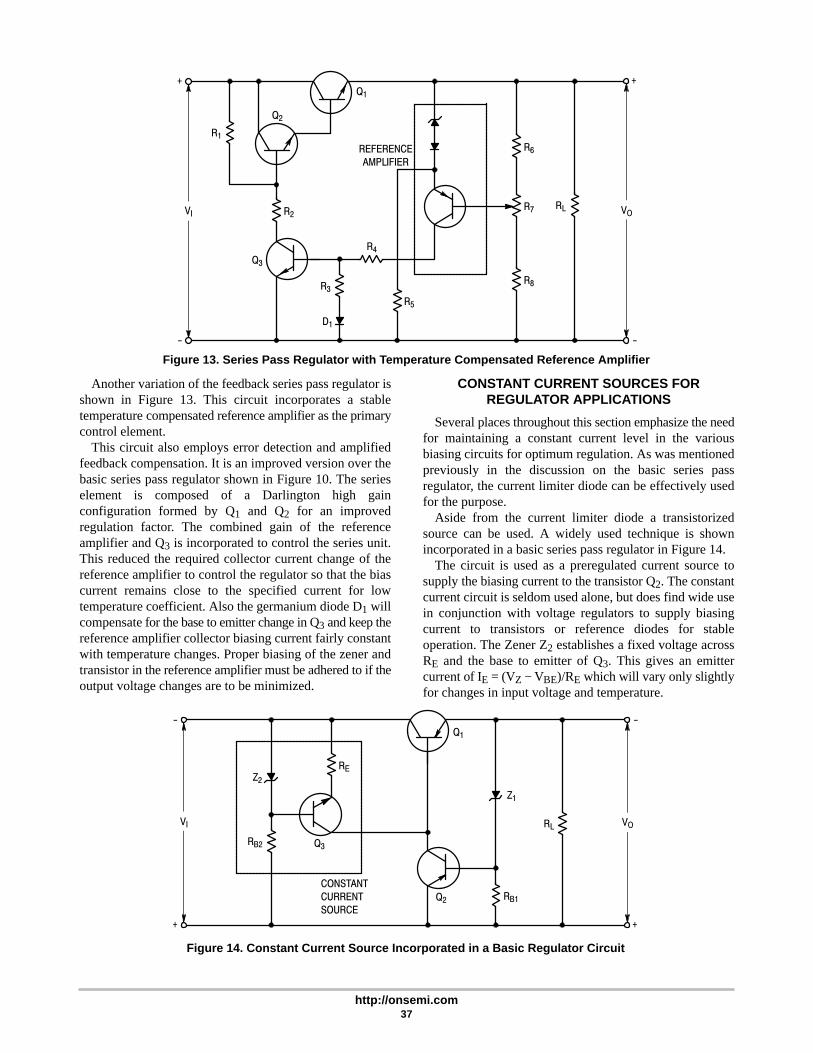
http://onsemi.com37
Figure 13. Series Pass Regulator with Temperature Compensated Reference Amplifier
+
-
+
-
R1
R2RL
R3
R5
R4
R8
R6
R7
D1
Q1
Q2
Q3
REFERENCEAMPLIFIER
VI VO
Another variation of the feedback series pass regulator isshown in Figure 13. This circuit incorporates a stabletemperature compensated reference amplifier as the primarycontrol element.
This circuit also employs error detection and amplifiedfeedback compensation. It is an improved version over thebasic series pass regulator shown in Figure 10. The serieselement is composed of a Darlington high gainconfiguration formed by Q1 and Q2 for an improvedregulation factor. The combined gain of the referenceamplifier and Q3 is incorporated to control the series unit.This reduced the required collector current change of thereference amplifier to control the regulator so that the biascurrent remains close to the specified current for lowtemperature coefficient. Also the germanium diode D1 willcompensate for the base to emitter change in Q3 and keep thereference amplifier collector biasing current fairly constantwith temperature changes. Proper biasing of the zener andtransistor in the reference amplifier must be adhered to if theoutput voltage changes are to be minimized.
CONSTANT CURRENT SOURCES FORREGULATOR APPLICATIONS
Several places throughout this section emphasize the needfor maintaining a constant current level in the variousbiasing circuits for optimum regulation. As was mentionedpreviously in the discussion on the basic series passregulator, the current limiter diode can be effectively usedfor the purpose.
Aside from the current limiter diode a transistorizedsource can be used. A widely used technique is shownincorporated in a basic series pass regulator in Figure 14.
The circuit is used as a preregulated current source tosupply the biasing current to the transistor Q2. The constantcurrent circuit is seldom used alone, but does find wide usein conjunction with voltage regulators to supply biasingcurrent to transistors or reference diodes for stableoperation. The Zener Z2 establishes a fixed voltage acrossRE and the base to emitter of Q3. This gives an emittercurrent of IE = (VZ − VBE)/RE which will vary only slightlyfor changes in input voltage and temperature.
Figure 14. Constant Current Source Incorporated in a Basic Regulator Circuit
Q1
Q2
Q3
RB1
Z1
RL
REZ2
RB2
CONSTANTCURRENTSOURCE
--
++
VI VO
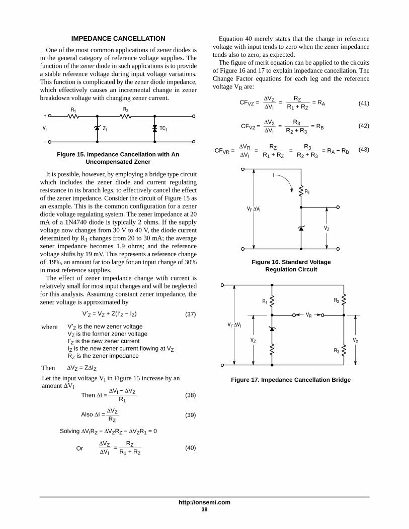
http://onsemi.com38
IMPEDANCE CANCELLATION
One of the most common applications of zener diodes isin the general category of reference voltage supplies. Thefunction of the zener diode in such applications is to providea stable reference voltage during input voltage variations.This function is complicated by the zener diode impedance,which effectively causes an incremental change in zenerbreakdown voltage with changing zener current.
Figure 15. Impedance Cancellation with AnUncompensated Zener
R2R1
Z1 TC1
+
-
VI
It is possible, however, by employing a bridge type circuitwhich includes the zener diode and current regulatingresistance in its branch legs, to effectively cancel the effectof the zener impedance. Consider the circuit of Figure 15 asan example. This is the common configuration for a zenerdiode voltage regulating system. The zener impedance at 20mA of a 1N4740 diode is typically 2 ohms. If the supplyvoltage now changes from 30 V to 40 V, the diode currentdetermined by R1 changes from 20 to 30 mA; the averagezener impedance becomes 1.9 ohms; and the referencevoltage shifts by 19 mV. This represents a reference changeof .19%, an amount far too large for an input change of 30%in most reference supplies.
The effect of zener impedance change with current isrelatively small for most input changes and will be neglectedfor this analysis. Assuming constant zener impedance, thezener voltage is approximated by
(37)V′Z = VZ + Z(I′Z − IZ)
where V′Z is the new zener voltageVZ is the former zener voltageI′Z is the new zener currentIZ is the new zener current flowing at VZRZ is the zener impedance
Then
Let the input voltage VI in Figure 15 increase by anamount ΔVI
Then ΔI =ΔVI − ΔVZ
R1
ΔVZ
RZAlso ΔI =
Solving ΔVIRZ − ΔVZRZ − ΔVZR1 = 0
ΔVZ
ΔVIOr =
RZ
R1 + RZ
(39)
(38)
(40)
ΔVZ = ZΔIZ
Equation 40 merely states that the change in referencevoltage with input tends to zero when the zener impedancetends also to zero, as expected.
The figure of merit equation can be applied to the circuitsof Figure 16 and 17 to explain impedance cancellation. TheChange Factor equations for each leg and the referencevoltage VR are:
(41)
(43)
(42)
CFVZ =ΔVZ
ΔVI
RZ
R1 + RZ= = RA
R3
R2 + R3
ΔV2
ΔVICFV2 = = = RB
RZ
R1 + RZ
ΔVR
ΔVICFVR = = = RA − RB
R3
R2 + R3=
Figure 16. Standard VoltageRegulation Circuit
R1
VI′ ΔVI
I
VZ
Figure 17. Impedance Cancellation Bridge
VI′ ΔVI
R3
R1 R2
VR
V2VZ
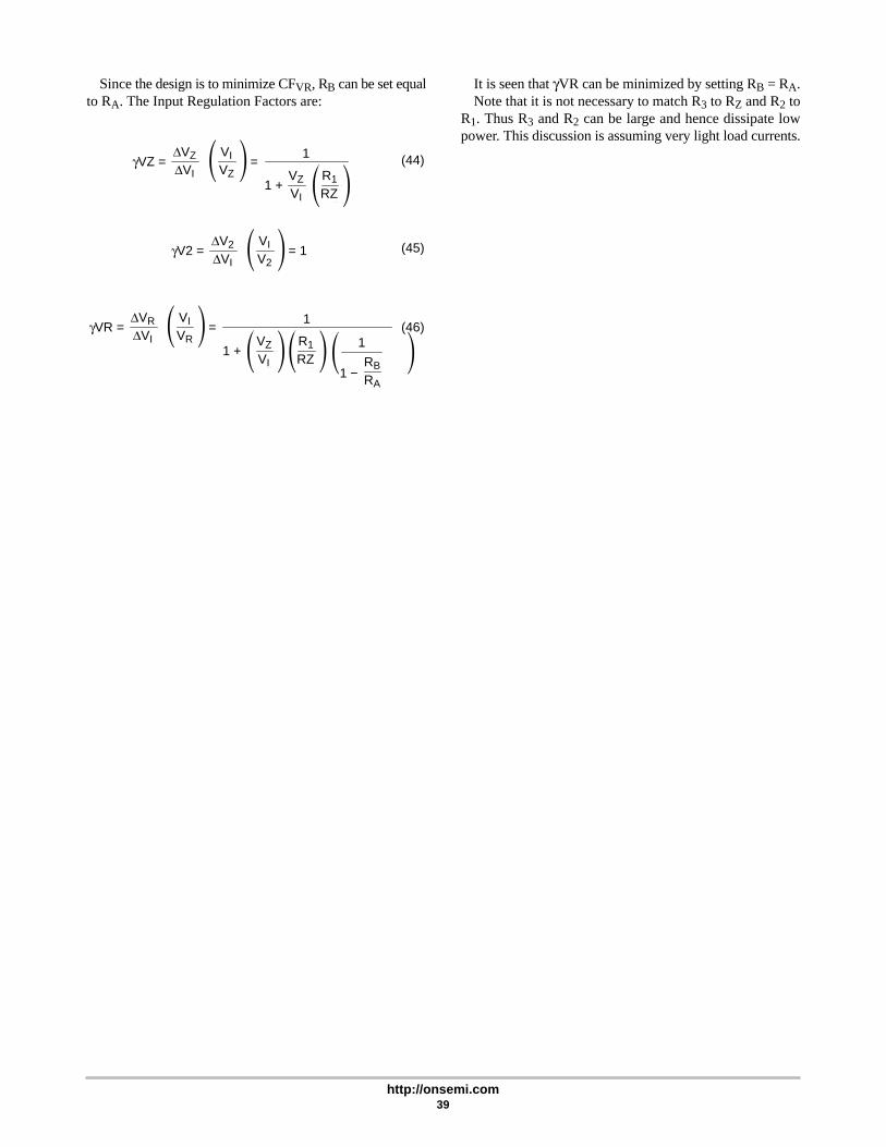
http://onsemi.com39
Since the design is to minimize CFVR, RB can be set equalto RA. The Input Regulation Factors are:
(44)
(46)
(45)
γVZ =ΔVZ
ΔVI� VI
ViZ� = 1VI
VZ1 +
VZ
VI� VI
ViZ�R1
RZ
γV2 =ΔV2
ΔVI� VI
ViZ� = 1
VI
V2
γVR =ΔVR
ΔVI� VI
ViZ� = 1VI
VR1 + � VI
ViZ�R1
RZ� VI
ViZ�VZ
VI� VI
Vi Z�1
1 −RB
RA
It is seen that γVR can be minimized by setting RB = RA.Note that it is not necessary to match R3 to RZ and R2 to
R1. Thus R3 and R2 can be large and hence dissipate lowpower. This discussion is assuming very light load currents.

http://onsemi.com40
ZENER VOLTAGE SENSING CIRCUITSAND APPLICATIONS
BASIC CONCEPTS OF VOLTAGE SENSING
Numerous electronic circuits require a signal or voltagelevel to be sensed for circuit actuation or function control.The circuit may alter its mode of operation whenever aninterdependent signal reaches a particular magnitude (eitherhigher or lower than a specified value). These sensingfunctions may be accomplished by incorporating a voltagedependent device in the system creating a switching actionthat controls the overall operation of the circuit.
The zener diode is ideally suited for most sensingapplications because of its voltage dependentcharacteristics. The following sections are some of the morecommon applications and techniques that utilize the zener ina voltage sensing capacity.
Figure 1. Basic Transistor-Zener DiodeSensing Circuits
R2
R1
R3
R1
R2Z1
R3
VIN
VINZ1 Q1
Q1
VO1
VO2
(a)
(b)
TRANSISTOR-ZENER SENSING CIRCUITS
The zener diode probably finds its greatest use in sensingapplications in conjunction with other semiconductordevices. Two basic widely used techniques are illustrated inFigures 1a and 1b.
In both of these circuits the output is a function of the inputvoltage level. As the input goes from low to high, the outputwill switch from either high to low (base sense circuit) orlow to high (emitter sense circuit), (see Figure 2).
The base sense circuit of Figure 1a operates as follows:When the input voltage is low, the voltage dropped across R2is not sufficient to bias the zener diode and base emitterjunction into conduction, therefore, the transistor will notconduct. This causes a high voltage from collector toemitter. When the input becomes high, the zener is biasedinto conduction, the transistor turns on, and the collector toemitter voltage, which is the output, drops to a low value.
Figure 2. Outputs of Transistor-Zener VoltageSensing Circuits
R2 + R1
R2VZ + VBE(SAT)VIN =
SENSING LEVEL
TIME
TIME
TIME
VIN BOTH CIRCUITS
VOUT BASE SENSE
VOUT EMITTER SENSE
VO2
VO1
VIN
(OUTPUT OF FIGURE 1b)
(OUTPUT OF FIGURE 1a)
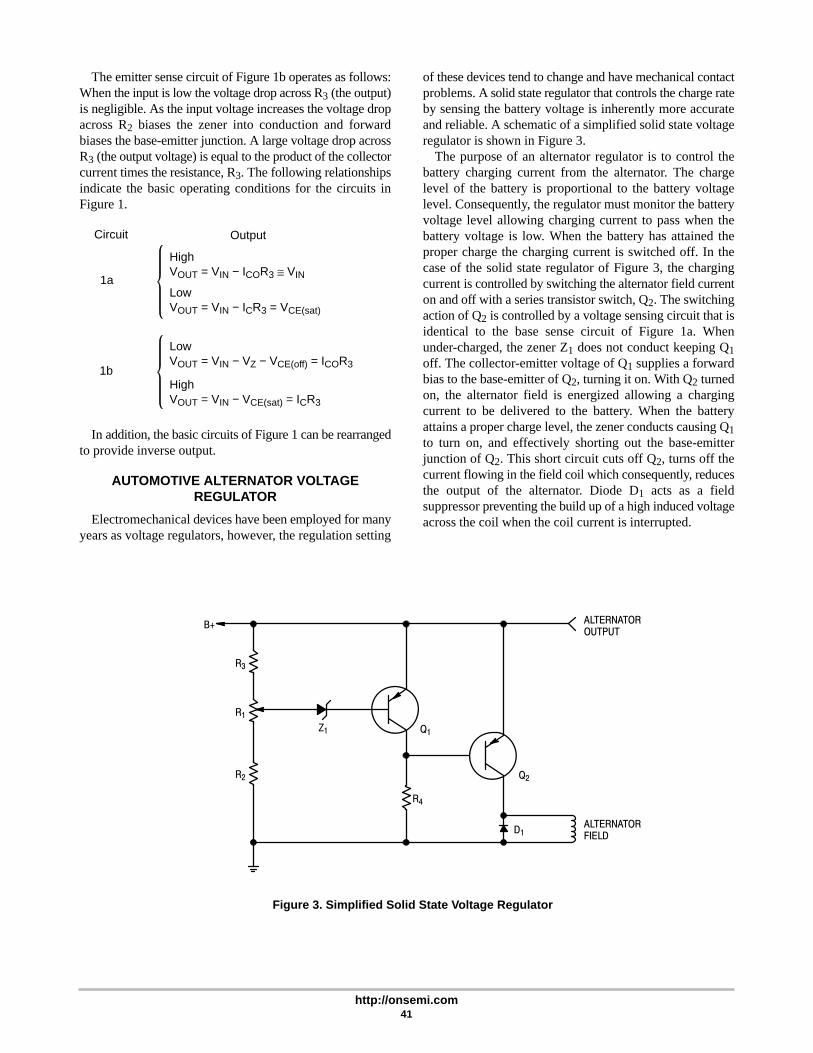
http://onsemi.com41
The emitter sense circuit of Figure 1b operates as follows:When the input is low the voltage drop across R3 (the output)is negligible. As the input voltage increases the voltage dropacross R2 biases the zener into conduction and forwardbiases the base-emitter junction. A large voltage drop acrossR3 (the output voltage) is equal to the product of the collectorcurrent times the resistance, R3. The following relationshipsindicate the basic operating conditions for the circuits inFigure 1.
Circuit Output
1a
1b
HighVOUT = VIN − ICOR3 ≅ VIN
LowVOUT = VIN − ICR3 = VCE(sat)
LowVOUT = VIN − VZ − VCE(off) = ICOR3
HighVOUT = VIN − VCE(sat) = ICR3
In addition, the basic circuits of Figure 1 can be rearrangedto provide inverse output.
AUTOMOTIVE ALTERNATOR VOLTAGEREGULATOR
Electromechanical devices have been employed for manyyears as voltage regulators, however, the regulation setting
of these devices tend to change and have mechanical contactproblems. A solid state regulator that controls the charge rateby sensing the battery voltage is inherently more accurateand reliable. A schematic of a simplified solid state voltageregulator is shown in Figure 3.
The purpose of an alternator regulator is to control thebattery charging current from the alternator. The chargelevel of the battery is proportional to the battery voltagelevel. Consequently, the regulator must monitor the batteryvoltage level allowing charging current to pass when thebattery voltage is low. When the battery has attained theproper charge the charging current is switched off. In thecase of the solid state regulator of Figure 3, the chargingcurrent is controlled by switching the alternator field currenton and off with a series transistor switch, Q2. The switchingaction of Q2 is controlled by a voltage sensing circuit that isidentical to the base sense circuit of Figure 1a. Whenunder-charged, the zener Z1 does not conduct keeping Q1off. The collector-emitter voltage of Q1 supplies a forwardbias to the base-emitter of Q2, turning it on. With Q2 turnedon, the alternator field is energized allowing a chargingcurrent to be delivered to the battery. When the batteryattains a proper charge level, the zener conducts causing Q1to turn on, and effectively shorting out the base-emitterjunction of Q2. This short circuit cuts off Q2, turns off thecurrent flowing in the field coil which consequently, reducesthe output of the alternator. Diode D1 acts as a fieldsuppressor preventing the build up of a high induced voltageacross the coil when the coil current is interrupted.
Figure 3. Simplified Solid State Voltage Regulator
R3
R1
R2
R4
B+
Z1 Q1
Q2
ALTERNATOROUTPUT
D1ALTERNATORFIELD
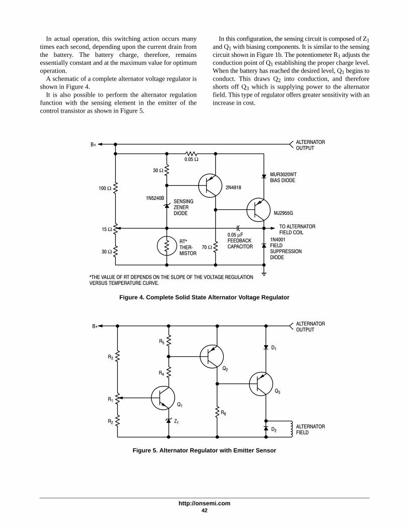
http://onsemi.com42
In actual operation, this switching action occurs manytimes each second, depending upon the current drain fromthe battery. The battery charge, therefore, remainsessentially constant and at the maximum value for optimumoperation.
A schematic of a complete alternator voltage regulator isshown in Figure 4.
It is also possible to perform the alternator regulationfunction with the sensing element in the emitter of thecontrol transistor as shown in Figure 5.
In this configuration, the sensing circuit is composed of Z1and Q1 with biasing components. It is similar to the sensingcircuit shown in Figure 1b. The potentiometer R1 adjusts theconduction point of Q1 establishing the proper charge level.When the battery has reached the desired level, Q1 begins toconduct. This draws Q2 into conduction, and thereforeshorts off Q3 which is supplying power to the alternatorfield. This type of regulator offers greater sensitivity with anincrease in cost.
Figure 4. Complete Solid State Alternator Voltage Regulator
Figure 5. Alternator Regulator with Emitter Sensor
B+
100 Ω
15 Ω
30 Ω
30 Ω
70 Ω
1N5240BSENSINGZENERDIODE
RT*THER‐MISTOR
0.05 μFFEEDBACKCAPACITOR
1N4001FIELDSUPPRESSIONDIODE
TO ALTERNATORFIELD COIL
MJ2955G
MUR3020WTBIAS DIODE
ALTERNATOROUTPUT
0.05 Ω
2N4918
*THE VALUE OF RT DEPENDS ON THE SLOPE OF THE VOLTAGE REGULATIONVERSUS TEMPERATURE CURVE.
B+ ALTERNATOROUTPUT
D2
D1
Q3
R5
R4Q2
R6
Z1
Q1
R3
R1
R2ALTERNATORFIELD
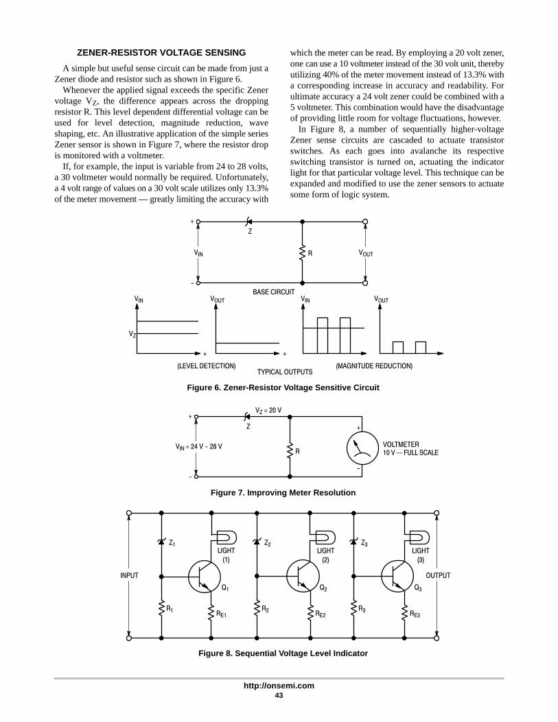
http://onsemi.com43
ZENER-RESISTOR VOLTAGE SENSING
A simple but useful sense circuit can be made from just aZener diode and resistor such as shown in Figure 6.
Whenever the applied signal exceeds the specific Zenervoltage VZ, the difference appears across the droppingresistor R. This level dependent differential voltage can beused for level detection, magnitude reduction, waveshaping, etc. An illustrative application of the simple seriesZener sensor is shown in Figure 7, where the resistor dropis monitored with a voltmeter.
If, for example, the input is variable from 24 to 28 volts,a 30 voltmeter would normally be required. Unfortunately,a 4 volt range of values on a 30 volt scale utilizes only 13.3%of the meter movement — greatly limiting the accuracy with
which the meter can be read. By employing a 20 volt zener,one can use a 10 voltmeter instead of the 30 volt unit, therebyutilizing 40% of the meter movement instead of 13.3% witha corresponding increase in accuracy and readability. Forultimate accuracy a 24 volt zener could be combined with a5 voltmeter. This combination would have the disadvantageof providing little room for voltage fluctuations, however.
In Figure 8, a number of sequentially higher-voltageZener sense circuits are cascaded to actuate transistorswitches. As each goes into avalanche its respectiveswitching transistor is turned on, actuating the indicatorlight for that particular voltage level. This technique can beexpanded and modified to use the zener sensors to actuatesome form of logic system.
Figure 6. Zener-Resistor Voltage Sensitive Circuit
Figure 7. Improving Meter Resolution
+
-
Z
R
BASE CIRCUIT
VZ
+ +
VIN VOUT VIN VOUT
(LEVEL DETECTION) (MAGNITUDE REDUCTION)
Z
R
+
-
+
-
VZ = 20 V
VOLTMETER10 V — FULL SCALE
TYPICAL OUTPUTS
VIN VOUT
VIN = 24 V - 28 V
Figure 8. Sequential Voltage Level Indicator
Z1
Q1 Q2 Q3
R1 R2 R3RE2RE1 RE3
Z2 Z3LIGHT
(1)LIGHT
(2)LIGHT
(3)
INPUT OUTPUT
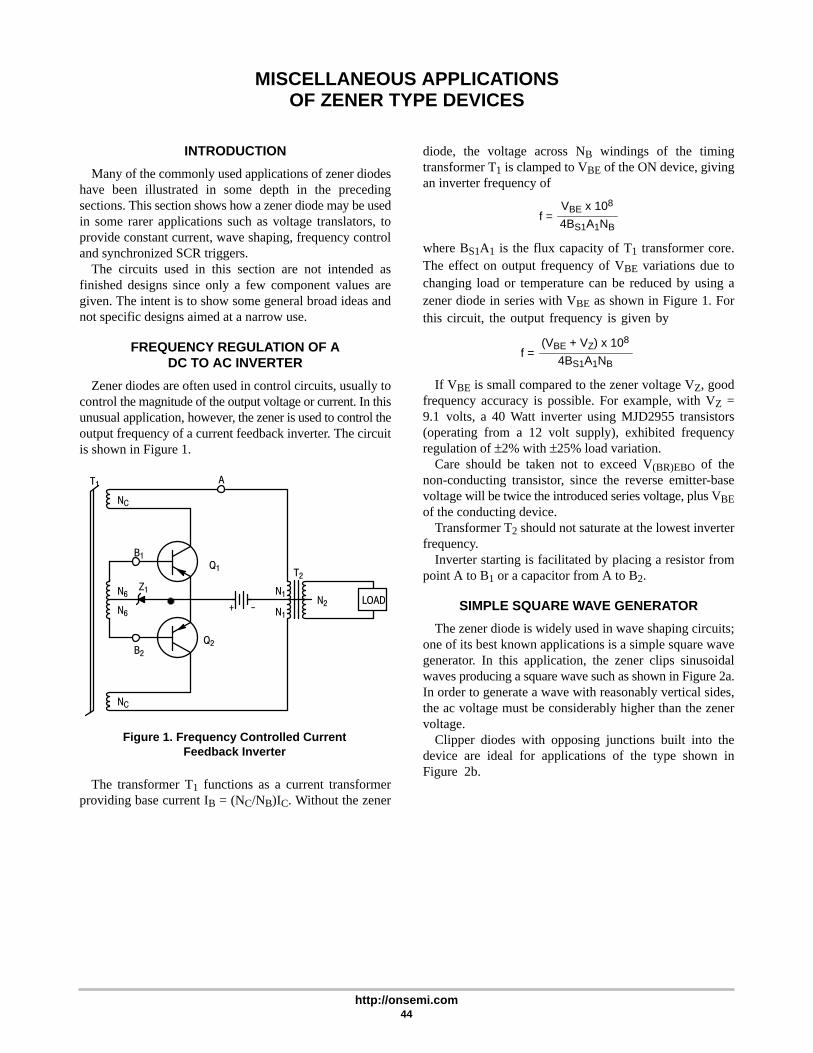
http://onsemi.com44
MISCELLANEOUS APPLICATIONSOF ZENER TYPE DEVICES
INTRODUCTION
Many of the commonly used applications of zener diodeshave been illustrated in some depth in the precedingsections. This section shows how a zener diode may be usedin some rarer applications such as voltage translators, toprovide constant current, wave shaping, frequency controland synchronized SCR triggers.
The circuits used in this section are not intended asfinished designs since only a few component values aregiven. The intent is to show some general broad ideas andnot specific designs aimed at a narrow use.
FREQUENCY REGULATION OF ADC TO AC INVERTER
Zener diodes are often used in control circuits, usually tocontrol the magnitude of the output voltage or current. In thisunusual application, however, the zener is used to control theoutput frequency of a current feedback inverter. The circuitis shown in Figure 1.
Figure 1. Frequency Controlled CurrentFeedback Inverter
Z1
Q1
Q2
T1
NC
N6
N6
NC
B1
B2
+
A
-
N1
N1
N2
T2
LOAD
The transformer T1 functions as a current transformerproviding base current IB = (NC/NB)IC. Without the zener
diode, the voltage across NB windings of the timingtransformer T1 is clamped to VBE of the ON device, givingan inverter frequency of
f =VBE x 108
4BS1A1NB
where BS1A1 is the flux capacity of T1 transformer core.The effect on output frequency of VBE variations due tochanging load or temperature can be reduced by using azener diode in series with VBE as shown in Figure 1. Forthis circuit, the output frequency is given by
f =(VBE + VZ) x 108
4BS1A1NB
If VBE is small compared to the zener voltage VZ, goodfrequency accuracy is possible. For example, with VZ =9.1 volts, a 40 Watt inverter using MJD2955 transistors(operating from a 12 volt supply), exhibited frequencyregulation of ±2% with ±25% load variation.
Care should be taken not to exceed V(BR)EBO of thenon-conducting transistor, since the reverse emitter-basevoltage will be twice the introduced series voltage, plus VBEof the conducting device.
Transformer T2 should not saturate at the lowest inverterfrequency.
Inverter starting is facilitated by placing a resistor frompoint A to B1 or a capacitor from A to B2.
SIMPLE SQUARE WAVE GENERATOR
The zener diode is widely used in wave shaping circuits;one of its best known applications is a simple square wavegenerator. In this application, the zener clips sinusoidalwaves producing a square wave such as shown in Figure 2a.In order to generate a wave with reasonably vertical sides,the ac voltage must be considerably higher than the zenervoltage.
Clipper diodes with opposing junctions built into thedevice are ideal for applications of the type shown inFigure 2b.
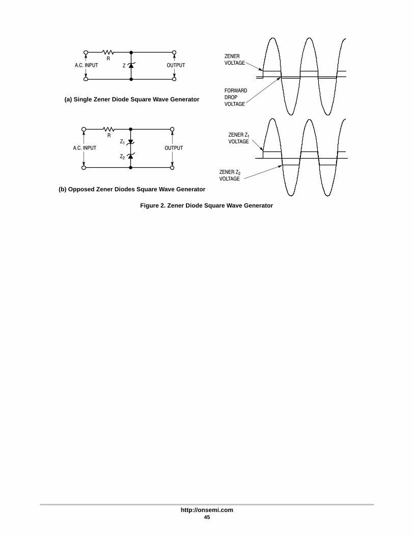
http://onsemi.com45
(a) Single Zener Diode Square Wave Generator
(b) Opposed Zener Diodes Square Wave Generator
Figure 2. Zener Diode Square Wave Generator
Z1
Z
Z2
R
R
ZENERVOLTAGE
FORWARDDROPVOLTAGE
ZENER Z1VOLTAGE
ZENER Z2VOLTAGE
A.C. INPUT OUTPUT
A.C. INPUT OUTPUT
http://onsemi.com46
MEASUREMENT OF ZENER VOLTAGE TO THERMAL EQUILIBRIUMWITH PULSED TEST CURRENT
INTRODUCTION
This paper discusses the zener voltage correlationproblem which sometimes exists between the manufacturerand the customer’s incoming inspection. A method is shownto aid in the correlation of zener voltage between thermalequilibrium and pulse testing. A unique double pulsedsample and hold test circuit is presented which improves theaccuracy of correlation.1
Several zener voltages versus zener pulsed test currentcurves are shown for four package styles. An appendix isattached for incoming inspection groups giving detailedinformation on tolerances involved in correlation.
For many years the major difficulty with zener diodetesting seemed to be correlation of tight tolerance voltagespecifications where accuracy between different test setupswas the main problem. The industry standard and the EIARegistration system adopted thermal equilibrium testing ofzener diodes as the basic test condition unless otherwisespecified. Thermal equilibrium was chosen because it wasthe most common condition in the final circuit design and itwas the condition that the design engineers needed for theircircuit design and device selection. Thermal equilibriumtesting was also fairly simple to set-up for sample testing atincoming inspection of standard tolerance zeners.
In recent years with the advent of economicalcomputerized test systems many incoming inspection areashave implemented computer testing of zener diodes whichhas been generating a new wave of correlation problemsbetween customers and suppliers of zener diodes.
The computerized test system uses short duration pulsetest techniques for testing zener diodes which does notdirectly match the industry standard thermal equilibriumtest specifications.
This paper was prepared in an attempt to clarify thedifferences between thermal equilibrium and short durationpulse testing of zener diodes, to provide a test circuit thatallows evaluation at various pulse widths and a suggestedprocedure for incoming inspection areas that will allowmeaningful correlation between thermal equilibrium andpulse testing.
In the measurement of zener voltage (VZ), thetemperature coefficient effect combined with test currentheating can present a problem if one is attempting tocorrelate VZ measurements made by another party (FinalTest, Quality Assurance or Incoming Inspection).2 Thispaper is intended as an aid in determining VZ at some testcurrent (IZT) pulse width other than the pulse width used bythe manufacturer.
Thermal equilibrium (TE) is reached when diode junctiontemperature has stabilized and no further change will occurin VZ if the IZT time is increased.2 This absolute value canvary depending on the mounting method and amount ofheatsinking. Therefore, thermal equilibrium conditionshave to be defined before meaningful correlation can exist.
Normalized VZ curves are shown for four package stylesand for three to five voltage ratings per package. Pulsewidths from 1 ms up to 100 seconds were used to arrive ator near thermal equilibrium for all packages with a givenmethod of mounting.
Mounting
There are five conditions that can affect the correlation ofVZ measurements and are: 1) instrumentation, 2) TA, 3) IZTtime, 4) PD and 5) mounting. The importance of the firstfour conditions is obvious but the last one, mounting, canmake the difference between good and poor correlation. Themounting can have a very important part in VZ correlationas it controls the amount of heat and rate of heat removalfrom the diode by the mass and material in contact with thediode package.
Two glass axial lead packages (DO-35 and DO-41),curves (Figures 5 and 6) were measured with standardGrayhill clips and a modified version of the Grayhill clips topermit lead length adjustment.
Test Circuit
The test circuit (Figure 8) consists of standard CMOSlogic for pulse generation, inverting and delaying. The logicdrives three bipolar transistors for generation of the powerpulse for IZT. VZ is fed into an unique sample and hold (S/H)circuit consisting of two high input impedance operationalamplifiers and a field effect transistor switch.
For greater accuracy in VZ measurements using a singlepulse test current, the FET switch is double pulsed. Doublepulsing the FET switch for charging the S/H capacitorincreases accuracy of the charge on the capacitor as thesecond pulse permits charging the capacitor closer to thefinal value of VZ.
The timing required for the two pulse system is shown inwaveform G-3C whereby the initial sample pulse is delayedfrom time zero by a fixed 100 μs to allow settling time andthe second pulse is variable in time to measure the analoginput at that particular point. The power pulse (waveformG-2D) must also encompass the second sample pulse.
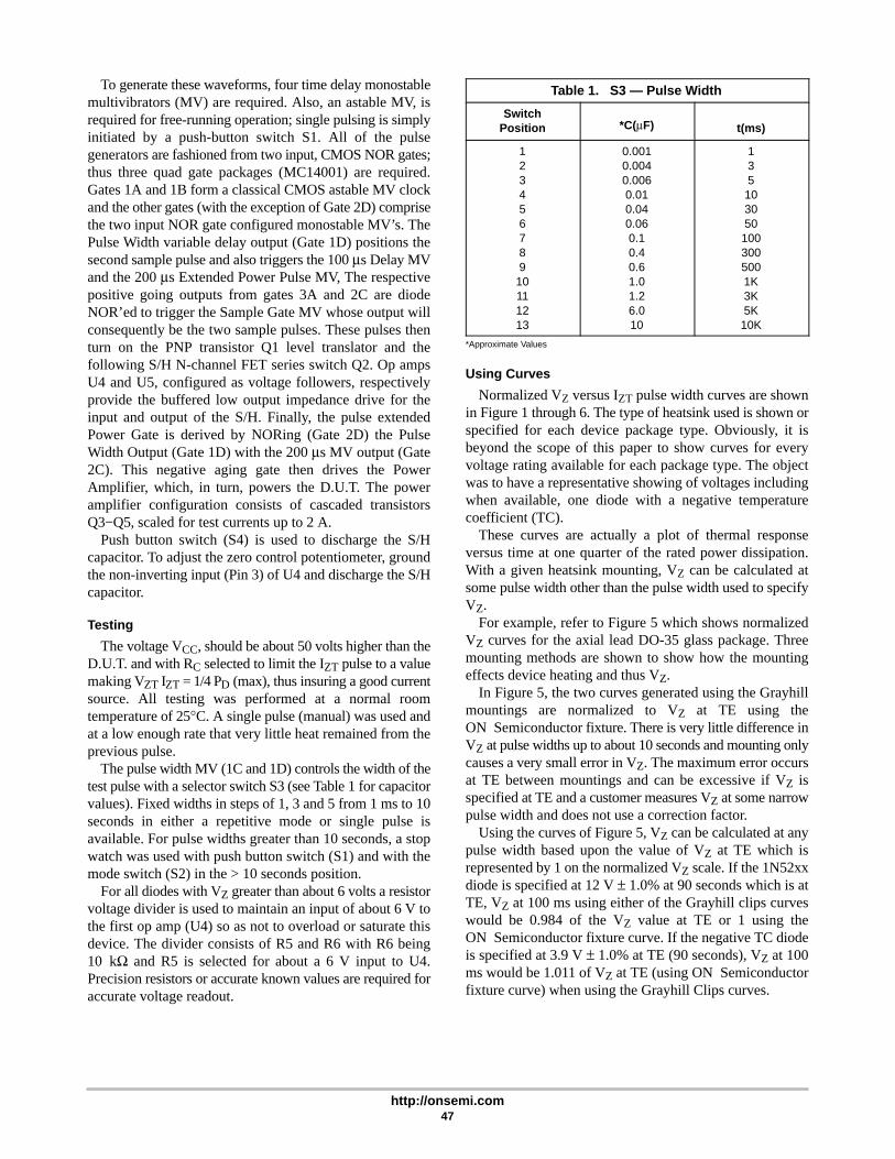
http://onsemi.com47
To generate these waveforms, four time delay monostablemultivibrators (MV) are required. Also, an astable MV, isrequired for free-running operation; single pulsing is simplyinitiated by a push-button switch S1. All of the pulsegenerators are fashioned from two input, CMOS NOR gates;thus three quad gate packages (MC14001) are required.Gates 1A and 1B form a classical CMOS astable MV clockand the other gates (with the exception of Gate 2D) comprisethe two input NOR gate configured monostable MV’s. ThePulse Width variable delay output (Gate 1D) positions thesecond sample pulse and also triggers the 100 μs Delay MVand the 200 μs Extended Power Pulse MV, The respectivepositive going outputs from gates 3A and 2C are diodeNOR’ed to trigger the Sample Gate MV whose output willconsequently be the two sample pulses. These pulses thenturn on the PNP transistor Q1 level translator and thefollowing S/H N-channel FET series switch Q2. Op ampsU4 and U5, configured as voltage followers, respectivelyprovide the buffered low output impedance drive for theinput and output of the S/H. Finally, the pulse extendedPower Gate is derived by NORing (Gate 2D) the PulseWidth Output (Gate 1D) with the 200 μs MV output (Gate2C). This negative aging gate then drives the PowerAmplifier, which, in turn, powers the D.U.T. The poweramplifier configuration consists of cascaded transistorsQ3−Q5, scaled for test currents up to 2 A.
Push button switch (S4) is used to discharge the S/Hcapacitor. To adjust the zero control potentiometer, groundthe non-inverting input (Pin 3) of U4 and discharge the S/Hcapacitor.
Testing
The voltage VCC, should be about 50 volts higher than theD.U.T. and with RC selected to limit the IZT pulse to a valuemaking VZT IZT = 1/4 PD (max), thus insuring a good currentsource. All testing was performed at a normal roomtemperature of 25°C. A single pulse (manual) was used andat a low enough rate that very little heat remained from theprevious pulse.
The pulse width MV (1C and 1D) controls the width of thetest pulse with a selector switch S3 (see Table 1 for capacitorvalues). Fixed widths in steps of 1, 3 and 5 from 1 ms to 10seconds in either a repetitive mode or single pulse isavailable. For pulse widths greater than 10 seconds, a stopwatch was used with push button switch (S1) and with themode switch (S2) in the > 10 seconds position.
For all diodes with VZ greater than about 6 volts a resistorvoltage divider is used to maintain an input of about 6 V tothe first op amp (U4) so as not to overload or saturate thisdevice. The divider consists of R5 and R6 with R6 being10 kΩ and R5 is selected for about a 6 V input to U4.Precision resistors or accurate known values are required foraccurate voltage readout.
Table 1. S3 — Pulse Width
SwitchPosition *C(μF) t(ms)
12345678910111213
0.0010.0040.0060.010.040.060.10.40.61.01.26.010
1351030501003005001K3K5K10K
*Approximate Values
Using Curves
Normalized VZ versus IZT pulse width curves are shownin Figure 1 through 6. The type of heatsink used is shown orspecified for each device package type. Obviously, it isbeyond the scope of this paper to show curves for everyvoltage rating available for each package type. The objectwas to have a representative showing of voltages includingwhen available, one diode with a negative temperaturecoefficient (TC).
These curves are actually a plot of thermal responseversus time at one quarter of the rated power dissipation.With a given heatsink mounting, VZ can be calculated atsome pulse width other than the pulse width used to specifyVZ.
For example, refer to Figure 5 which shows normalizedVZ curves for the axial lead DO-35 glass package. Threemounting methods are shown to show how the mountingeffects device heating and thus VZ.
In Figure 5, the two curves generated using the Grayhillmountings are normalized to VZ at TE using theON Semiconductor fixture. There is very little difference inVZ at pulse widths up to about 10 seconds and mounting onlycauses a very small error in VZ. The maximum error occursat TE between mountings and can be excessive if VZ isspecified at TE and a customer measures VZ at some narrowpulse width and does not use a correction factor.
Using the curves of Figure 5, VZ can be calculated at anypulse width based upon the value of VZ at TE which isrepresented by 1 on the normalized VZ scale. If the 1N52xxdiode is specified at 12 V ± 1.0% at 90 seconds which is atTE, VZ at 100 ms using either of the Grayhill clips curveswould be 0.984 of the VZ value at TE or 1 using theON Semiconductor fixture curve. If the negative TC diodeis specified at 3.9 V ± 1.0% at TE (90 seconds), VZ at 100ms would be 1.011 of VZ at TE (using ON Semiconductorfixture curve) when using the Grayhill Clips curves.

http://onsemi.com48
In using the curves of Figure 5 and 6, it should be kept inmind that VZ can be different at TE for the three mountingsbecause diode junction temperature can be different for eachmounting at TE which is represented by 1 on the VZnormalized scale. Therefore, when the correlation of VZbetween parties is attempted, they must use the same type ofmounting or know what the delta VZ is between the twomountings involved.
The Grayhill clips curves in Figure 6 are normalized to theON Semiconductor fixture at TE as in Figure 5. Figures 1through 4 are normalized to VZ at TE for each diode andwould be used as Figures 5 and 6.
Measurement accuracy can be affected by test equipment,power dissipation of the D.U.T., ambient temperature andaccuracy of the voltage divider if used on the input of the firstop-amp (U4). The curves of Figures 1 through 6 are for anambient temperature of 25°C, at other ambients, θVZ has tobe considered and is shown on the data sheet for the 1N52xxseries of diodes. θVZ is expressed in mV/°C and ismultiplied by the difference in TA from the 25°C value andeither subtracted or added to the calculated VZ dependingupon whether the diode has a negative or positive TC.
General Discussion
The TC of zener diodes can be either negative or positive,depending upon die processing. Generally, devices with abreakdown voltage greater than about 5 V have a positiveTC and diodes under about 5 V have a negative TC.
Conclusion
Curves showing VZ versus IZT pulse width can be used tocalculate VZ at a pulse width other than the one used tospecify VZ. A test circuit and method is presented to obtainVZ with a single pulse of test current to generate VZ curvesof interest.
References
1. Al Pshaenich, “Double Pulsing S/H Increases SystemAccuracy”; Electronics, June 16, 1983.
2. ON Semiconductor Zener Diode Manual, Series A,1980.
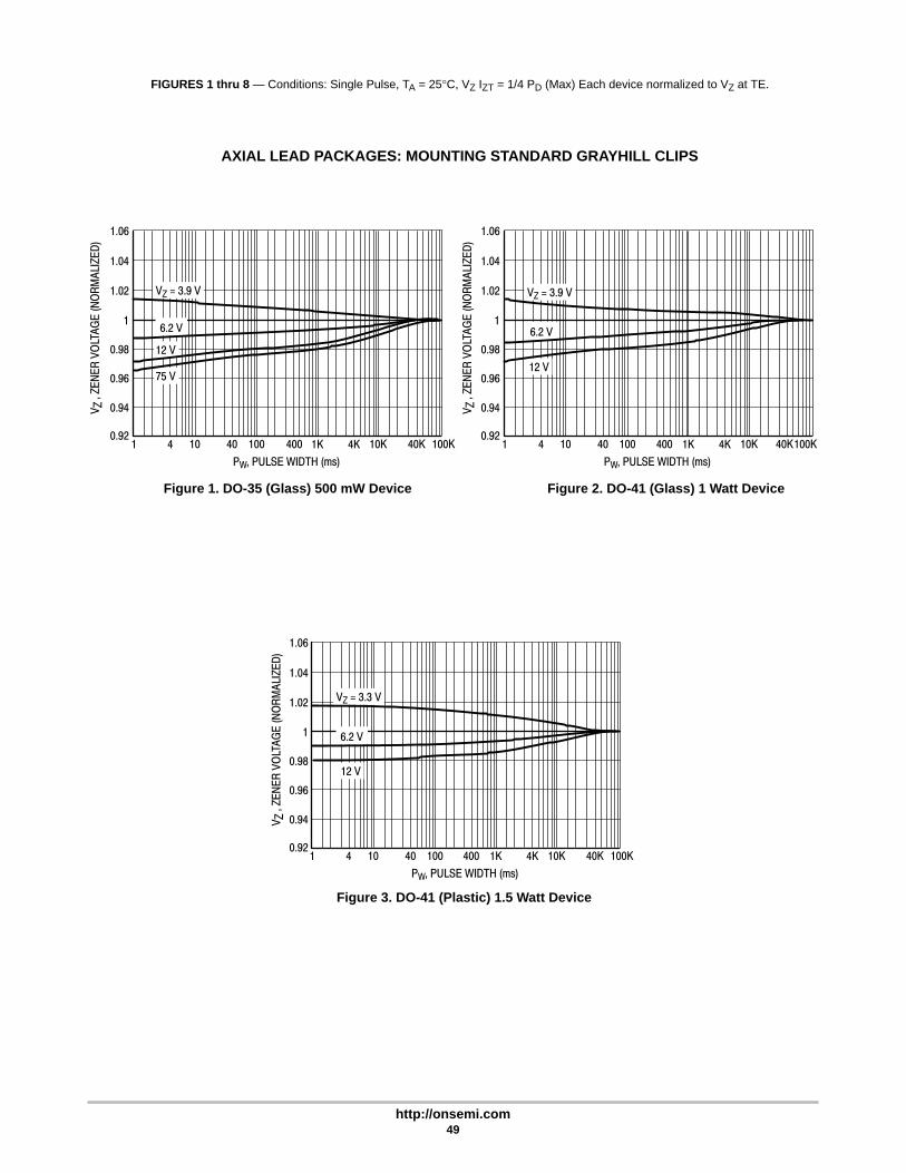
http://onsemi.com49
FIGURES 1 thru 8 — Conditions: Single Pulse, TA = 25°C, VZ IZT = 1/4 PD (Max) Each device normalized to VZ at TE.
AXIAL LEAD PACKAGES: MOUNTING STANDARD GRAYHILL CLIPS
Figure 1. DO-35 (Glass) 500 mW Device Figure 2. DO-41 (Glass) 1 Watt Device
Figure 3. DO-41 (Plastic) 1.5 Watt Device
V ,
ZEN
ER V
OLT
AGE
(NO
RM
ALIZ
ED)
Z
VZ = 3.9 V
6.2 V
12 V
1.06
1.04
1.02
1
0.98
0.96
0.94
0.9210 40 1001 4 400 1K 4K 10K 40K 100K
PW, PULSE WIDTH (ms)
75 V
1.06
1.04
1.02
1
0.98
0.96
0.94
0.92
V ,
ZEN
ER V
OLT
AGE
(NO
RM
ALIZ
ED)
Z
10 40 1001 4 400 1K 4K 10K 40K100K
PW, PULSE WIDTH (ms)
VZ = 3.9 V
6.2 V
12 V
V ,
ZEN
ER V
OLT
AGE
(NO
RM
ALIZ
ED)
Z
VZ = 3.3 V
6.2 V
12 V
1.06
1.04
1.02
1
0.98
0.96
0.94
0.9210 40 1001 4 400 1K 4K 10K 40K 100K
PW, PULSE WIDTH (ms)

http://onsemi.com50
THREE MOUNTING METHODS: DO-35 AND DO-41
Figure 4. DO-35 (Glass) 500 mW Device
Figure 5. DO-41 (Glass) 1 Watt Device
Figure 6. Standard Grayhill Clips
MOUNTING FIXTURE
1N5242B (VZ = 12 V)
1N5228B (VZ = 3.9 V)
GRAYHILL CLIPSSTANDARD, L = 11/16″
ON SEMICONDUCTORFIXTURE L = 1/2″
MOUNTINGS:
MODIFIEDL = 3/8″
1.022
1.018
1.014
1.012
1.008
1.004
1
0.996
10 40 1001 4 400 1K 4K 10K 40K 100K
0.992
0.988
0.984
0.98
0.976
0.972
0.968
V ,
ZEN
ER V
OLT
AGE
(NO
RM
ALIZ
ED)
Z
PW, PULSE WIDTH (ms)
1.004
1
10 40 1001 400 1K 4K 10K 40K 100K
0.992
0.988
0.984
0.98
0.9764
0.996
MOUNTINGS:GRAYHILL CLIPS
STANDARD, L = 11/16″MODIFIED, L = 3/8″
ON SEMICONDUCTORFIXTUREL = 1/2″
1N4742A
VZ = 12 V
V ,
ZEN
ER V
OLT
AGE
(NO
RM
ALIZ
ED)
Z
PW, PULSE WIDTH (ms)
1.41
1.69
.78
.75
2.31
GRAYHILL CLIPSMODIFIED, L = 3/8″
STANDARD,L = 11/16″
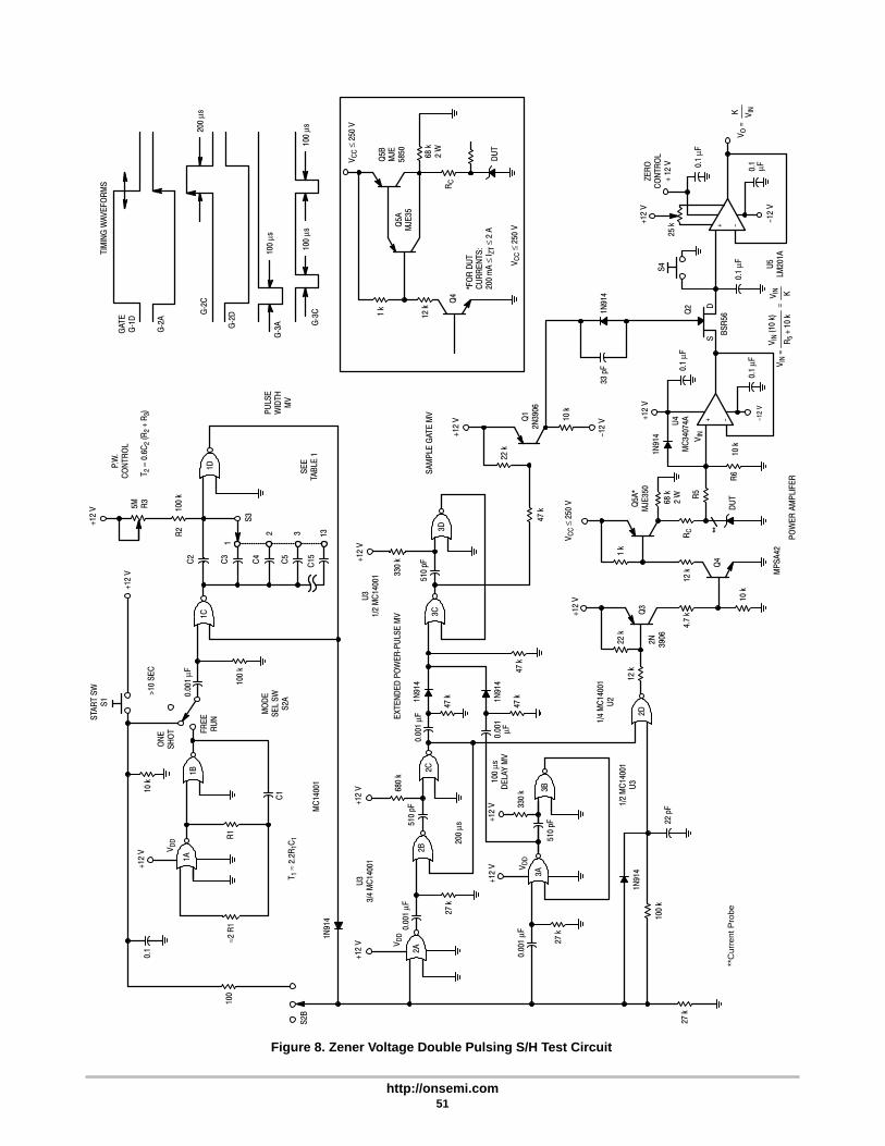
http://onsemi.com51
Figure 8. Zener Voltage Double Pulsing S/H Test Circuit
3B
3D3C
2C
1D
0.1
+12
V
1A1B
1C
2A2B
3A
2D
100
100
k22
pF
1N91
4
1/2
MC
1400
1U
312
k22
k
4.7
k
10 k
12 k
1 k
Q4
MPS
A42
POW
ER A
MPL
IFER
RC
R5
68 k
2 W
DU
T
**
Q5A
*M
JE35
0
R6
10 k
1N91
4
U4
MC
3407
4AV I
N+ - -1
2 V
0.1
μF
BSR
56
SD
Q2
0.1
μF
S4
0.1
μF
-12
V
0.1
μF0.1
μF
V O =
V INK
ZER
OC
ON
TRO
L+
12 V
25 k
V IN
=V I
N (1
0 k)
R5
+ 10
k
V IN K
=
+12
VV C
C ≤
250
V
1N91
433
pF
-12
V10 k
22 k
47 k
Q1
2N39
06
+12
V
SAM
PLE
GAT
E M
V51
0 pF
330
k
U3
1/2
MC
1400
1
+12
V
EXTE
ND
ED P
OW
ER‐P
ULS
E M
V
1N91
4
47 k
47 k
0.00
1μF
47 k1N
914
0.00
1 μF
200
μs
+12
V 680
k
510
pF
27 k
+12
VU
33/
4 M
C14
001
0.00
1 μF
V DD
510
pF
330
k
+12
V
V DD
+12
V
0.00
1 μF
27 k
100
μsD
ELAY
MV
1/4
MC
1400
1U
2
S2B
≈2 R
1R
1
C1
V DD
T 1 ≈
2.2
R1C
1
MC
1400
11N
914
MO
DE
SEL
SWS2
A
10 k
ON
ESH
OT
0.00
1 μF
>10
SEC
STAR
T SW
S1
+12
V
+12
V
100
k
FREE
RU
N
C2
C4
C5
C15C3
100
kR
2
5M R3
P.W
.C
ON
TRO
L
T 2 ≈
0.6
C2
(R2
+ R
3)
1
S3
SEE
TABL
E 1
PULS
EW
IDTH
MV
2 3 13
27 k
TIM
ING
WAV
EFO
RM
S
GAT
EG
‐1D
G‐2
A
G‐2
C
G‐2
D
G‐3
A G‐3
C
100
μs
100
μs10
0 μs20
0 μs
2N 3906
Q3
+ -
+12
V+1
2 V
U5
LM20
1A
**C
urre
nt P
robe
1 k
12 k
68 k
2 W
RC
Q4
*FO
R D
UT
CU
RR
ENTS
:20
0 m
A ≤
I ZT
≤ 2
A
V CC
≤ 2
50 V
DU
T
Q5A
MJE
35
Q5B
MJE
5850
V CC
≤ 2
50 V
http://onsemi.com52
APPENDIX ARecommended Incoming Inspection Procedures
Zener Voltage TestingPulsed versus Thermal Equilibrium
This section is primarily for use of incoming inspectiongroups. The subject covered is the measurement of zenervoltage (VZ) and the inherent difficulty of establishingcorrelation between supplier and buyer when using pulsedtest techniques. This difficulty, in part, is due to theinterpretation of the data taken from the variety of availabletesters and in some cases even from the same model types.It is therefore, our intent to define and reestablish astandardized method of measurement to achieve correlationno matter what test techniques are being used. Thisstandardization will guarantee your acceptance of goodproduct while maintaining reliable correlation.
DEFINITION OF TERMS
Temperature Coefficient (TC):
The temperature stability of zener voltages is sometimesexpressed by means of the temperature coefficient (TC).This parameter is usually defined as the percent voltagechange across the device per degree centigrade, or as aspecific voltage change per degree centigrade. Temperaturechanges during test are due to the self heating effects causedby the dissipation of power in the zener junction. The VZ willchange due to this temperature change and will exhibit apositive or negative TC, depending on the zener voltage.Generally, devices with a zener voltage below five volts willhave a negative TC and devices above five volts will exhibita positive TC.
Thermal Equilibrium (TE)
Thermal equilibrium (TE) is reached when the diodejunction temperature has stabilized and no further changewill occur. In thermal equilibrium, the heat generated at thejunction is removed as rapidly as it is created, hence, nofurther temperature changes.
MEASURING ZENER VOLTAGE
The zener voltage, being a temperature dependentparameter, needs to be controlled for valid VZ correlation.Therefore, so that a common base of comparison can beestablished, a reliable measure of VZ can only occur whenall possible variables are held constant. This common baseis achieved when the device under test has had sufficienttime to reach thermal equilibrium (heatsinking is required tostabilize the lead or case temperature to a specified value for
stable junction temperatures). The device should also bepowered from a constant current source to limit changes ofpower dissipated and impedance.
All of the above leads us to an understanding of whyvarious pulse testers will give differing VZ readings; thesedifferences are, in part, due to the time duration of test (pulsewidth), duty cycle when data logging, contact resistance,tolerance, temperature, etc. To resolve all of this, one onlyneeds a reference standard to compare their pulsed resultsagainst and then adjust their limits to reflect thosedifferences. It should be noted that in a large percentage ofapplications the zener diode is used in thermal equilibrium.
ON Semiconductor guarantees all of it’s axial leadedzener products (unless otherwise specified) to be withinspecification ninety (90) seconds after the application ofpower while holding the lead temperatures at 30 ± 1°C, 3/8of an inch from the device body, any fixture that will meetthat criteria will correlate. 30°C was selected over thenormally specified 25°C because of its ease of maintenance(no environmental chambers required) in a normal roomambient. A few degrees variation should have negligibleeffect in most cases. Hence, a moderate to large heatsink inmost room ambients should suffice.
Also, it is advisable to limit extraneous air movementsacross the device under test as this could change thermalequilibrium enough to affect correlation.
SETTING PULSED TESTER LIMITS
Pulsed test techniques do not allow a sufficient time forzener junctions to reach TE. Hence, the limits need to be setat different values to reflect the VZ at lower junctiontemperatures. Since there are many varieties of test systemsand possible heatsinks, the way to establish these limits is toactually measure both TE and pulsed VZ on a serializedsample for correlation.
The following examples show typical delta changes inpulsed versus TE readings. The actual values you use forpulsed conditions will depend on your tester. Note, that thereare examples for both positive and negative temperaturecoefficients. When setting the computer limits for a positiveTC device, the largest difference is subtracted from theupper limit and the smallest difference is subtracted from thelower limit. In the negative coefficient example the largestchange is added to the lower limit and the smallest changeis added to the upper limit.
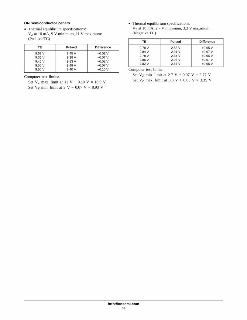
http://onsemi.com53
ON Semiconductor Zeners
• Thermal equilibrium specifications:VZ at 10 mA, 9 V minimum, 11 V maximum:(Positive TC)
TE Pulsed Difference
9.53 V9.35 V9.46 V9.56 V9.50 V
9.45 V9.38 V9.83 V9.49 V9.40 V
−0.08 V−0.07 V−0.08 V−0.07 V−0.10 V
Computer test limits:Set VZ max. limit at 11 V − 0.10 V = 10.9 VSet VZ min. limit at 9 V − 0.07 V = 8.93 V
• Thermal equilibrium specifications:VZ at 10 mA, 2.7 V minimum, 3.3 V maximum:(Negative TC)
TE Pulsed Difference
2.78 V2.84 V2.78 V2.86 V2.82 V
2.83 V2.91 V2.84 V2.93 V2.87 V
+0.05 V+0.07 V+0.05 V+0.07 V+0.05 V
Computer test limits:Set VZ min. limit at 2.7 V + 0.07 V = 2.77 VSet VZ max. limit at 3.3 V + 0.05 V = 3.35 V
© Semiconductor Components Industries, LLC, 2005
April, 2005 − Rev. 154 Publication Order Number:
NLAS3158/DHBD854/D
ON Semiconductor and are trademarks of Semiconductor Components Industries, LLC dba ON Semiconductor or its subsidiaries in the United States and/or other countries.ON Semiconductor owns the rights to a number of patents, trademarks, copyrights, trade secrets, and other intellectual property. A listing of ON Semiconductor’s product/patentcoverage may be accessed at www.onsemi.com/site/pdf/Patent− Marking.pdf. ON Semiconductor reserves the right to make changes without further notice to any products herein.ON Semiconductor makes no warranty, representation or guarantee regarding the suitability of its products for any particular purpose, nor does ON Semiconductor assume any liabilityarising out of the application or use of any product or circuit, and specifically disclaims any and all liability, including without limitation special, consequential or incidental damages.Buyer is responsible for its products and applications using ON Semiconductor products, including compliance with all laws, regulations and safety requirements or standards,regardless of any support or applications information provided by ON Semiconductor. “Typical” parameters which may be provided in ON Semiconductor data sheets and/orspecifications can and do vary in different applications and actual performance may vary over time. All operating parameters, including “Typicals” must be validated for each customerapplication by customer’s technical experts. ON Semiconductor does not convey any license under its patent rights nor the rights of others. ON Semiconductor products are notdesigned, intended, or authorized for use as a critical component in life support systems or any FDA Class 3 medical devices or medical devices with a same or similar classificationin a foreign jurisdiction or any devices intended for implantation in the human body. Should Buyer purchase or use ON Semiconductor products for any such unintended orunauthorized application, Buyer shall indemnify and hold ON Semiconductor and its officers, employees, subsidiaries, affiliates, and distributors harmless against all claims, costs,damages, and expenses, and reasonable attorney fees arising out of, directly or indirectly, any claim of personal injury or death associated with such unintended or unauthorizeduse, even if such claim alleges that ON Semiconductor was negligent regarding the design or manufacture of the part. ON Semiconductor is an Equal Opportunity/Affirmative ActionEmployer. This literature is subject to all applicable copyright laws and is not for resale in any manner.
PUBLICATION ORDERING INFORMATIONN. American Technical Support: 800−282−9855 Toll FreeUSA/Canada
Europe, Middle East and Africa Technical Support:Phone: 421 33 790 2910
Japan Customer Focus CenterPhone: 81−3−5817−1050
LITERATURE FULFILLMENT:Literature Distribution Center for ON Semiconductor19521 E. 32nd Pkwy, Aurora, Colorado 80011 USAPhone: 303−675−2175 or 800−344−3860 Toll Free USA/CanadaFax: 303−675−2176 or 800−344−3867 Toll Free USA/CanadaEmail: [email protected]
ON Semiconductor Website: www.onsemi.com
Order Literature: http://www.onsemi.com/orderlit
For additional information, please contact your localSales Representative
◊
Copyright © 2022 FDOKUMEN