ADVANCED SEMICONDUCTOR LASERS
134
INSTITUT NATIONAL DES SCIENCES APPLIQUÉES ADVANCED SEMICONDUCTOR LASERS Frédéric Grillot Université Européenne de Bretagne Laboratoire CNRS FOTON 20 avenue des buttes de Coesmes 35043 Rennes Cedex [email protected] Second Version - Year 2010
-
Upload
khangminh22 -
Category
Documents
-
view
0 -
download
0
Transcript of ADVANCED SEMICONDUCTOR LASERS

INSTITUT NATIONAL DES SCIENCES APPLIQUÉES
ADVANCED SEMICONDUCTOR LASERS
Frédéric Grillot
Université Européenne de BretagneLaboratoire CNRS FOTON
20 avenue des buttes de Coesmes35043 Rennes Cedex
Second Version - Year 2010

2
Contents
1 Basics of Semiconductor Lasers 71.1 Principle of Operation . . . . . . . . . . . . . . . . . . . . . . . . . . . . . . . 7
1.1.1 Radiative Transitions in a Semiconductor . . . . . . . . . . . . . . . . . 71.1.2 Optical Gain and Laser Cavity . . . . . . . . . . . . . . . . . . . . . . 91.1.3 Output Light-Current Characteristic . . . . . . . . . . . . . . . . . . . 111.1.4 Carrier Confinement . . . . . . . . . . . . . . . . . . . . . . . . . . . . 131.1.5 Optical Field Confinement and Spatial Modes . . . . . . . . . . . . . . 151.1.6 Near- and Far-Field Patterns . . . . . . . . . . . . . . . . . . . . . . . 17
1.2 Quantum Well Lasers . . . . . . . . . . . . . . . . . . . . . . . . . . . . . . . . 181.3 Quantum Dot Lasers . . . . . . . . . . . . . . . . . . . . . . . . . . . . . . . . 201.4 Single-Frequency Lasers . . . . . . . . . . . . . . . . . . . . . . . . . . . . . . 23
1.4.1 Short-Cavity Lasers . . . . . . . . . . . . . . . . . . . . . . . . . . . . . 231.4.2 Coupled-Cavity Lasers . . . . . . . . . . . . . . . . . . . . . . . . . . . 231.4.3 Injection-Locked Lasers . . . . . . . . . . . . . . . . . . . . . . . . . . . 241.4.4 DBR Lasers . . . . . . . . . . . . . . . . . . . . . . . . . . . . . . . . . 251.4.5 DFB Lasers . . . . . . . . . . . . . . . . . . . . . . . . . . . . . . . . . 26
2 Advances in Measurements of Physical Parameters of Semiconductor Lasers 312.1 Measurements of the Optical Gain . . . . . . . . . . . . . . . . . . . . . . . . . 31
2.1.1 Determination of the Optical Gain from the Amplified SpontaneousEmission . . . . . . . . . . . . . . . . . . . . . . . . . . . . . . . . . . . 32
2.1.2 Determination of the Optical Gain from the True Spontaneous Emission 342.2 Measurement of the Optical Loss . . . . . . . . . . . . . . . . . . . . . . . . . 362.3 Measurement of the Carrier Leakage in Semiconductor Lasers . . . . . . . . . 37
2.3.1 Optical Technique of Studying the Carrier Leakage . . . . . . . . . . . 372.3.2 Electrical Technique of Studying Carrier Leakage . . . . . . . . . . . . 38
2.4 Electrical and Optical Measurements of RFModulation Response below Thresh-old . . . . . . . . . . . . . . . . . . . . . . . . . . . . . . . . . . . . . . . . . . 402.4.1 Determination of the Carrier Lifetime from the Device Impedance . . . 41
3

CONTENTS
2.4.2 Determination of the Carrier Lifetime from the Optical Response Mea-surements . . . . . . . . . . . . . . . . . . . . . . . . . . . . . . . . . . 43
2.5 Optical Measurements of RF Modulation Response and RIN above threshold . 442.5.1 Determination of the Resonant Frequency and Differential Gain from
the RIN Measurements . . . . . . . . . . . . . . . . . . . . . . . . . . . 472.6 Measurements of the linewidth enhancement factor . . . . . . . . . . . . . . . 49
2.6.1 Definition . . . . . . . . . . . . . . . . . . . . . . . . . . . . . . . . . . 502.6.2 Measurement Techniques of the α-factor . . . . . . . . . . . . . . . . . 522.6.3 Measurements of linewidth enhancement factor from ASE and TSE
spectra . . . . . . . . . . . . . . . . . . . . . . . . . . . . . . . . . . . . 592.7 Measurements of the Carrier Temperature and Carrier Heating in Semicon-
ductor Lasers . . . . . . . . . . . . . . . . . . . . . . . . . . . . . . . . . . . . 61
3 Ultrafast Diode Lasers in Fiber Optics Communications 653.1 High-Speed Modulation of Laser Diodes . . . . . . . . . . . . . . . . . . . . . 65
3.1.1 Small-Signal Modulation Response . . . . . . . . . . . . . . . . . . . . 663.2 Nonlinear Gain Effects . . . . . . . . . . . . . . . . . . . . . . . . . . . . . . . 69
3.2.1 Origin and Definition . . . . . . . . . . . . . . . . . . . . . . . . . . . . 693.2.2 Evaluation of the Gain Compression in Quantum Dot/Dash Devices . . 713.2.3 Consequences on the Linewidth Enhancement Factor . . . . . . . . . . 73
3.3 Quantum-Well Lasers and Carrier-Transport Effects . . . . . . . . . . . . . . . 773.4 Large-Signal Effects . . . . . . . . . . . . . . . . . . . . . . . . . . . . . . . . . 813.5 Spectral Broadening and Spectral Control Under High-Speed Modulation . . . 83
3.5.1 Frequency Chirping . . . . . . . . . . . . . . . . . . . . . . . . . . . . . 833.5.2 Low-Chirp Lasers . . . . . . . . . . . . . . . . . . . . . . . . . . . . . . 83
3.6 Fundamental Limitations . . . . . . . . . . . . . . . . . . . . . . . . . . . . . . 843.6.1 Power Limitation . . . . . . . . . . . . . . . . . . . . . . . . . . . . . . 853.6.2 Dispersion Limitation . . . . . . . . . . . . . . . . . . . . . . . . . . . . 863.6.3 Timing Jitter Limitation . . . . . . . . . . . . . . . . . . . . . . . . . . 86
4 Gain and Q-Switching in Semiconductor Lasers 894.1 Gain Switching . . . . . . . . . . . . . . . . . . . . . . . . . . . . . . . . . . . 89
4.1.1 Principle of Operation . . . . . . . . . . . . . . . . . . . . . . . . . . . 894.1.2 Pulsewidth and Peak Power . . . . . . . . . . . . . . . . . . . . . . . . 914.1.3 Optical Spectra and Frequency Chirping . . . . . . . . . . . . . . . . . 93
4.2 Q-Switching in Laser Diodes . . . . . . . . . . . . . . . . . . . . . . . . . . . . 964.2.1 Active Q-Switching . . . . . . . . . . . . . . . . . . . . . . . . . . . . . 964.2.2 Passive Q-Switching . . . . . . . . . . . . . . . . . . . . . . . . . . . . 98
4

CONTENTS
4.2.3 Optical Spectra . . . . . . . . . . . . . . . . . . . . . . . . . . . . . . . 99
5 Mode-Locked Semiconductor Lasers 1015.1 Principle of Operation . . . . . . . . . . . . . . . . . . . . . . . . . . . . . . . 1025.2 Active Mode-Locking . . . . . . . . . . . . . . . . . . . . . . . . . . . . . . . . 1025.3 Passive-Mode Locking . . . . . . . . . . . . . . . . . . . . . . . . . . . . . . . 1045.4 Colliding Pulse Mode-Locking . . . . . . . . . . . . . . . . . . . . . . . . . . . 1095.5 Monolithic Quantum Dot Passively Mode-Locked Lasers . . . . . . . . . . . . 1115.6 Colliding Pulse Technique for Higher Order Harmonic Generation . . . . . . . 114
6 Injection-Locking of Semiconductor Diode Lasers 1176.1 Introduction . . . . . . . . . . . . . . . . . . . . . . . . . . . . . . . . . . . . . 1176.2 Applications of Optically-Injected Lasers . . . . . . . . . . . . . . . . . . . . . 1196.3 Theoretical Description . . . . . . . . . . . . . . . . . . . . . . . . . . . . . . . 124
6.3.1 Rate Equations . . . . . . . . . . . . . . . . . . . . . . . . . . . . . . . 1256.3.2 Steady-State Solutions . . . . . . . . . . . . . . . . . . . . . . . . . . . 1266.3.3 Small-Signal Analysis . . . . . . . . . . . . . . . . . . . . . . . . . . . . 1266.3.4 Modulation Response Model . . . . . . . . . . . . . . . . . . . . . . . . 1276.3.5 Identifying the Known Free-Running Operating Parameters . . . . . . . 129
6.4 Experimental Data and Curve-Fitting Results . . . . . . . . . . . . . . . . . . 1306.4.1 Experimental Setup and Data . . . . . . . . . . . . . . . . . . . . . . . 1306.4.2 Model Based Analysis . . . . . . . . . . . . . . . . . . . . . . . . . . . 131
5

CONTENTS
6

Chapter 1
Basics of Semiconductor Lasers
There exist a number of books devoted to semiconductor lasers in which the reader willfind the story of the invention of diode lasers in the early 1960s reporting all the details onstimulated emission, gain, and absorption in semiconductors, waveguide properties, varioussemiconductor materials for lasers, a description of different laser structures and so on. Inthis chapter, we shall try to give a brief description of the principle of operation of laserdiodes and some physical phenomena that are common to all types of semiconductor lasers.Finally, this chapter is shall pay special attention to some of the present-day laser devicesthat are most often used for ultra-short optical pulse generation and numerous applications.
1.1 Principle of Operation
1.1.1 Radiative Transitions in a Semiconductor
The quantum electronics concepts common to all lasers are combined in the semiconductorlaser with the basic pn junction that is typical of many semiconductor devices. Semiconductorlaser action relies upon the interband recombination of charge carriers (electrons and holes)and the subsequent liberation of photons. Applying a forward bias on a pn junction by usingan external voltage makes possible a diffusion and drift of electrons and holes across thejunction. In a narrow depletion region, electron-holes pairs can recombine either radiativelyor nonradiatively. Electrons and holes can also absorb the radiation. When the currentthrough the junction exceeds a critical value, a population inversion is achieved and the rateof photon emission due to electron-hole recombination exceeds the rate of absorption due toelectron-hole generation.The electronic radiative transitions that take place between the conduction and valence bands
7

Chapter 1. Basics of Semiconductor Lasers
in a semiconductor laser play roles very similar to those that take place between pairs ofstates in a simple two-level laser system. However there are several obvious features of asemiconductor active medium. First, for semiconductors the optical transitions are betweena continuous band of states within the valence and conduction bands. Then, the interactionbetween the different excited states in the band of a semiconductor is considerably greaterthan the interaction between the excited states of different atoms in the two-level system.Thus, collision processes in the electron and hole subsystems occur much faster and thatthe intraband relaxation times can be much shorter compared to those of the radiation(interband) processes. Intraband processes play crucial roles in line broadening in laserdiodes. Another difference is that the higher concentration of electronic states in the bandsprovides the potential for a higher optical gain. Finally, in the semiconductor the excitedelectron-hole pairs can be transported through the material by conduction or diffusion leadingto a spatial variation of the optical mode through the stimulated emission.The band structure of a typical III-V semiconductor and radiative transitions are shown infigure 1.1. For laser diodes, the transition from the conduction band to the valence one should
Figure 1.1: A realistic band model for a III-V direct gap semiconductor
be radiative and yield a photon with energy:
h̄ω = E2 − E1 (1.1)
where h̄ is the Planck’s constant and E1, E2 are the electron energy in the valence andconductive bands. As stated by the rules of the quantum mechanics, it can be shown thateach process must conserve both the energy and wavevector k. Due to the fact that the photon
8

1.1. Principle of Operation
wave number is at least two orders of magnitude lower (for visible and near infrared radiations)compared to the electron and hole wavevectors, the radiation transition is described in figure1.1 as a vertical line. The k-conservation rule immediately implies a requirement for directband-gap semiconductors if we want the radiative recombination to be significant. It can beshown using the Fermi-Dirac statistics of electrons and holes in a semiconductor that for netstimulated emission or optical gain, the separation of quasi-Fermi levels for electrons Fc andholes Fv must be:
Fc − Fv > h̄ω (1.2)
Inequality (1.2) was introduced by Bernard and Durrafourg, French researchers from the Cen-tre National des Télécommunications (CNET). This condition is necessary, but not sufficientfor laser action in a semiconductor. In order to achieve lasing, the stimulated emission ratemust be sufficient to overcome various loss mechanisms. The optical gain is related directlyto the rate of stimulated emission. The main factors influencing the gain spectrum are thedensity of states functions and the transition and occupation probabilities.
1.1.2 Optical Gain and Laser Cavity
A simple empirical formula for the optical gain g is obtained by assuming a linear dependenceon carrier concentration N and a parabolic variation with wavelength λ such as:
g = g0(N −Nt) + b(λ− λp)2 (1.3)
where g0 is the differential gain coefficient, Nt is the transparency density for which g = 0at λ = λp and N = Nt, b is related to the gain spectral width, and λp is the wavelengthcorresponding to the gain peak. As the carrier concentration is supposed to increase due tothe current injection, the photon energy at the gain peak shifts to higher values:
λp = λ0 + (N −Nt)dλ
dN(1.4)
The values for the above parameters can be obtained from measurements of gain spectra. Forinstance, for InGaAsP lasers, we will find λ0=1550 nm, g0=2.7 10−16cm2, b=0.15 cm−1nm−2,Nt=1.2 1018cm−3 and dλ
dN=-2.7 10−17 nm cm3.
The optical gain alone is not enough to operate a laser. Optical feedback is the other necessaryingredient. In laser diodes, optical feedback is provided in different ways. The simplest wayis to form a laser cavity by two cleaved facets of the diode, which actually are partiallyreflecting mirrors. Figure 1.2 illustrates a semiconductor laser that has two cleaved facetsfor optical feedback. The laser cavity provides a direction selectivity for the process ofstimulated emission because only photons traveling along its axis are reflected back and forthand experience maximum gain. It also provides a frequency selectivity since the feedback is
9

Chapter 1. Basics of Semiconductor Lasers
strongest for frequencies corresponding to the modes of the Fabry-Perot cavity. Althoughspontaneous and stimulated emission can occur while a current is applied to the junction,the laser does not generate coherent emission until the current exceeds a critical value, whichis known as the threshold current. In order to obtain the threshold conditions, it is requiredthat the optical field in the cavity reproduce itself after each round trip (steady-state orcontinuous-wave conditions). For the Fabry-Perot laser shown in figure 1.2, the thresholdconditions can be written as:
Γgth = αi + 12L ln
( 1R1R2
)(1.5)
βL = mπ (1.6)
where m is an integer, gth is the threshold gain, αi is the internal loss in the active layer
Figure 1.2: Schematic illustration of a Fabry-Perot diode laser. The light is emitted fromtwo partially reflecting cleaved facets of the diode
due to free-carrier absorption and scattering, L is the cavity length, R1 and R2 are the facetreflectivities and β is the propagation constant. The factor Γ is the optical confinement whichrepresents the fraction of the mode energy contained in the active layer. Thus, it accountsfor the reduction in gain due to the spreading of the optical mode to the cladding layerssurrounding the active layer.
Note: Internal loss αi can be written as a superposition of terms αi =Γαa + (1− Γ)αc + αs.
10

1.1. Principle of Operation
Coefficient αc accounts for loss in the confinement area and equals about 5 cm−1. The termαs ≈ 15cm−1 takes into account the scattering loss. Basically it is related to the qualityof the growth operation and especially the regrowth which is required for the realization ofburied ridge strip (BRS) structure. Coefficient αa accounts for the loss in the active zoneand depends on the transitions between valence bands. As a consequence, this coefficientis wavelength-dependent and equals 90 cm−1 at 1.55 µm and 60 cm−1 at 1.31µm. At thewavelength of 1.55 µm, it can be shown that αa = KN + αa0 with N the injected carrierdensity, αa0 ≈45 cm−1 and K=3.75 10−17 cm2 (values from experiments).
Equation (1.6) serves to extract the lasing frequency ω0 which is one of the cavity mode ωm:
ωm = mπc
nL(1.7)
and which is the nearest to the gain peak as shown in figure 1.3. In (1.7), n is the refractiveindex of the active layer and c the celerity of light in vacuum. In a laser diode, the refractiveindex n (phase optical index) varies with the frequency ω (material dispersion) and strictlyspeaking the intermode spacing δω is as follows:
δω = πc
nL(1.8)
The optical group index ng which is dependent on frequency can be expressed as,
ng = n+ ω∂n
∂ω(1.9)
The round-trip time δτ of the laser is related to δω following the relation:
δτ = 2πδω
= 2nLc
(1.10)
Let us consider the case of a 300µm long InGaAsP laser. In the wavelength range of 1.5µm, we have n=3.5 and ng=4. The longitudinal modes spacing is δν ≈100-150 GHz orδλ = λ2δν
c≈1 nm. Using typical values for Γ, αi, R1 and R2 in (1.5), a material gain of
about 100-150 cm−1 is required to achieve threshold conditions. The gain bandwidth ofsemiconductor lasers is very broad as compared with δν and in practice this generally resultsin multi-longitudinal mode operation. Normally, there are several modes that meet the phasecondition described by equation (1.6) and exhibit gains that are only slightly smaller (≈ 10−3-10−4) than the threshold gain (1.5). Single-mode operation can be achieved if the thresholdgain for the oscillating mode significantly smaller than that for the other modes.
1.1.3 Output Light-Current Characteristic
Let us now focus on the light-current characteristic (LCC) of semiconductor lasers. Theinterband radiative recombination leads to either spontaneous or stimulated emission. The
11

Chapter 1. Basics of Semiconductor Lasers
Figure 1.3: Schematic illustration of longitudinal modes and the gain profile of a Fabry-Perotdiode laser. The threshold is reached when the spontaneous emission and optical gain equalloss for the mode in the vicinity of the gain peak
electron-hole recombination rate R(N) can reasonably be written such as:
R(N) = AN +BN2 + CN3 +RstNph (1.11)
where Rst describes the net rate of stimulated emission, Nph is the intracavity photon densityand A, B, and C are the parameters of spontaneous recombination. The cubic term CN3
referred to as Auger recombination whose inclusion is of first importance for long-wavelengthsemiconductor lasers. The bimolecular coefficient B is know to be dependent on N and isoften approximated by B = B0−B1N . The stimulated emission term is directly proportionalto the optical gain,
Rst = c
ngg(N) (1.12)
Assuming a linear dependence of the optical gain on the carrier concentration, one obtainsfor the ideal LCC above the laser threshold the following relationship,
P (I) = h̄ω
2eαm
αm + αi(I − Ith) (1.13)
where e is the electronic charge and αm the mirror loss:
αm = 12L ln
( 1R1R2
)(1.14)
Equation (1.13) represents a linear LCC as the one shown in figure 1.4. The slope of the curveis reasonably constant until the power saturation mechanisms settle in (not shown in figure1.4). The saturation of the power is connected with the thermal heating of the device. The
12

1.1. Principle of Operation
threshold current Ith is dependent on the temperature T and its behavior can be empiricallydescribed as follows:
Ith ∝ exp(T/T0) (1.15)
T0 represents the characteristic temperature; typical values of T0 are in the range of 150-200Kfor GaAlAs lasers and 40-70K for InGaAsP lasers. Despite the temperature behavior of thethreshold current is a little bit more complicated, (1.15) gives a quite reasonable description.
Figure 1.4: The typical light-current characteristic (LCC) of semiconductor laser and thecorresponding output spectrum
1.1.4 Carrier Confinement
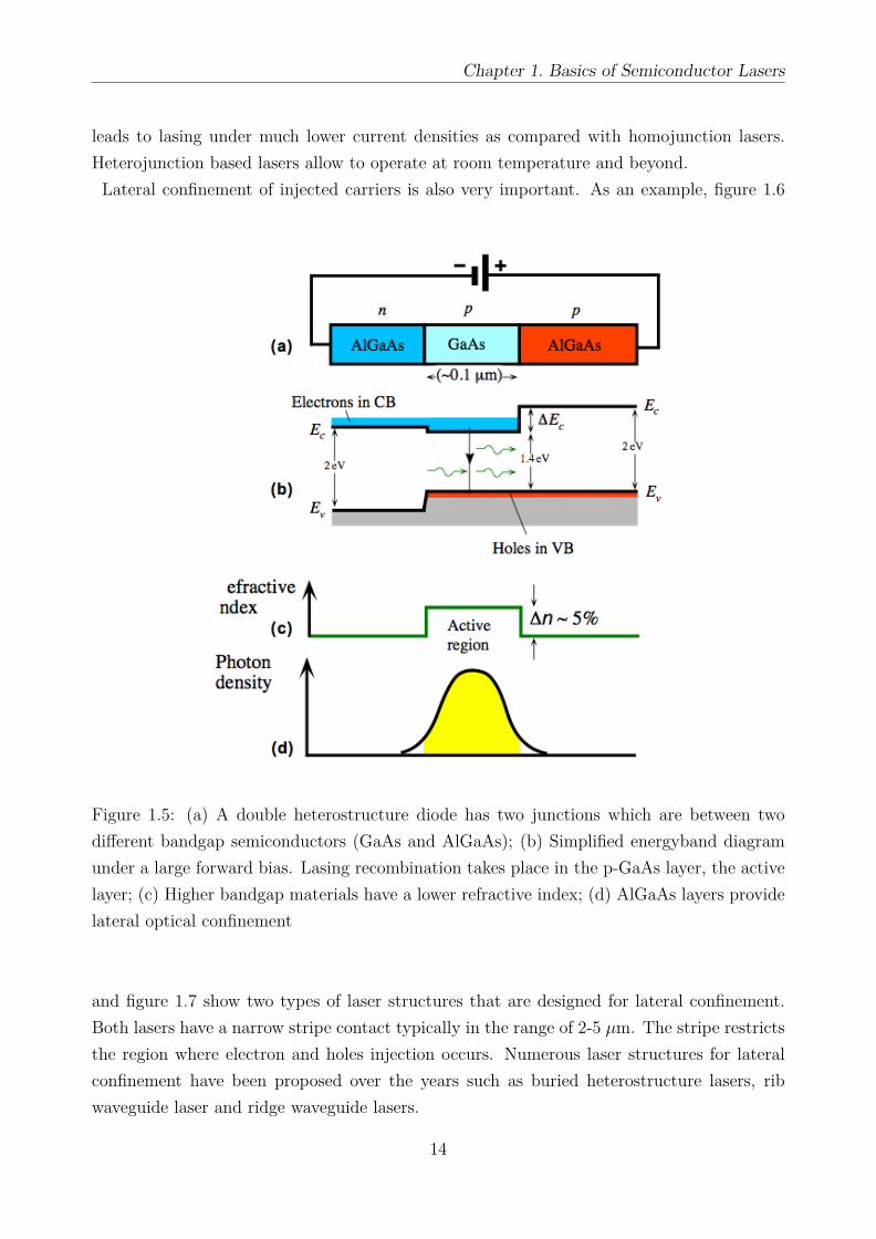
Although the pn junction can amplify the electromagnetic radiation and exhibits optical gainunder forward bias, the thickness of the region in which the gain is sufficiently high is verysmall (in the range of 0.01 µm). This is because there is no mechanism to confine carriers;usually homojunctions lasers failed to operate at room temperature. The carrier confinementin the plane perpendicular to the pn junction can be achieved using heterojunctions. Adouble heterojunction is used to prevent electron-hole spreading from the pn junction wherethe carriers recombine. Figure 1.5 shows the energy-band diagram of a double heterostructurelaser (DH). The active layer is sandwiched by two claddings layers that have wider band gaps.The pn junction is biased in the forward direction. Due to the external voltage, an injection ofholes from the p-doped layer and an injection of electron from the n-doped side occur into theactive layer. The potential barriers on the boundaries between the layers resulting from theband-gap differences prevent electrons and holes from spreading into the cladding layers. Theconcentration of minority carriers can easily reach very high values in the active layer. This
13
Chapter 1. Basics of Semiconductor Lasers
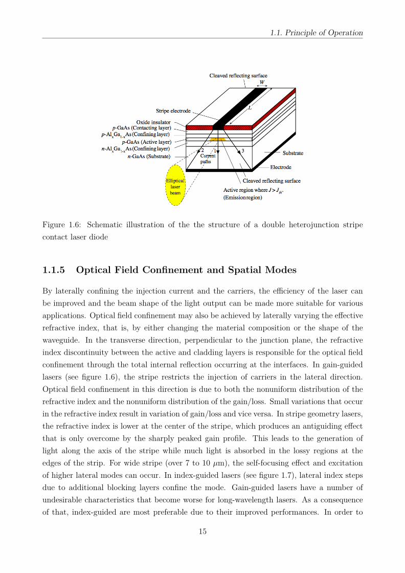
leads to lasing under much lower current densities as compared with homojunction lasers.Heterojunction based lasers allow to operate at room temperature and beyond.Lateral confinement of injected carriers is also very important. As an example, figure 1.6
Figure 1.5: (a) A double heterostructure diode has two junctions which are between twodifferent bandgap semiconductors (GaAs and AlGaAs); (b) Simplified energyband diagramunder a large forward bias. Lasing recombination takes place in the p-GaAs layer, the activelayer; (c) Higher bandgap materials have a lower refractive index; (d) AlGaAs layers providelateral optical confinement
and figure 1.7 show two types of laser structures that are designed for lateral confinement.Both lasers have a narrow stripe contact typically in the range of 2-5 µm. The stripe restrictsthe region where electron and holes injection occurs. Numerous laser structures for lateralconfinement have been proposed over the years such as buried heterostructure lasers, ribwaveguide laser and ridge waveguide lasers.
14
1.1. Principle of Operation
Figure 1.6: Schematic illustration of the the structure of a double heterojunction stripecontact laser diode
1.1.5 Optical Field Confinement and Spatial Modes
By laterally confining the injection current and the carriers, the efficiency of the laser canbe improved and the beam shape of the light output can be made more suitable for variousapplications. Optical field confinement may also be achieved by laterally varying the effectiverefractive index, that is, by either changing the material composition or the shape of thewaveguide. In the transverse direction, perpendicular to the junction plane, the refractiveindex discontinuity between the active and cladding layers is responsible for the optical fieldconfinement through the total internal reflection occurring at the interfaces. In gain-guidedlasers (see figure 1.6), the stripe restricts the injection of carriers in the lateral direction.Optical field confinement in this direction is due to both the nonuniform distribution of therefractive index and the nonuniform distribution of the gain/loss. Small variations that occurin the refractive index result in variation of gain/loss and vice versa. In stripe geometry lasers,the refractive index is lower at the center of the stripe, which produces an antiguiding effectthat is only overcome by the sharply peaked gain profile. This leads to the generation oflight along the axis of the stripe while much light is absorbed in the lossy regions at theedges of the strip. For wide stripe (over 7 to 10 µm), the self-focusing effect and excitationof higher lateral modes can occur. In index-guided lasers (see figure 1.7), lateral index stepsdue to additional blocking layers confine the mode. Gain-guided lasers have a number ofundesirable characteristics that become worse for long-wavelength lasers. As a consequenceof that, index-guided are most preferable due to their improved performances. In order to
15

Chapter 1. Basics of Semiconductor Lasers
Figure 1.7: Schematic illustration of the cross sectional structure of a buried heterostructurelaser diode
calculate the optical field confinement, the confinement factor Γ is normally introduced. Inthe transverse direction, values of this parameter can be calculated using a normalized activelayer thickness D,
D = 2πdλ
(n2 − n2c)1/2 (1.16)
where d is the true active layer thickness and n and nc are the refractive indices of the activeand cladding layers, respectively. As the value of D decreases, the optical wave spreads intothe cladding regions whereas at large values, the optical field gets extremely well-confinedand Γ approaches the unity. A useful approximation for the transverse confinement factorΓT accurate within 1.5% is given by,
ΓT = D2
2 +D2 (1.17)
To ensure single transverse-mode behavior, D must be less than π. Since typically d ≤0.2µm, the single transverse-mode condition is always satisfied in practical devices.The treatment of spatial modes is really different depending on whether gain guiding or indexguiding is used to confine the optical field. In gain-guided based devices, the carrier diffusionplays an important role and the carrier concentration is laterally nonuniform. Let us stressthat in general, a numerical approach is required to solve the problem of determining thelateral modes in gain-guided lasers. The number of lateral modes in such devices depends onthe strip width w. When w <10 µm, only the fundamental mode can be considered in thestructure. In case of strongly index-guided based lasers, it is possible to define the nomalizedwaveguide width W such as:
W = 2πwλ
(n2eff − n2
eff,c)1/2 (1.18)
16

1.1. Principle of Operation
where neff and neff,c are the effective indices of the active and cladding layers. In analogyto (1.17), the lateral confinement factor ΓL is given by,
ΓT = W 2
2 +W 2 (1.19)
The mode confinement factor Γ can be written as Γ = ΓLΓT . For index-guided lasers,typically w ≈2-3 µm, ΓL ≈1 and Γ =≈ ΓT . To summarize, it is just important to emphasizethat the problem of spatial modes in semiconductor laser is the problem of modes of a slabwaveguide based upon on the solutions of Maxwell’s equations. A slab waveguide can usuallysupport two types of modes named either transverse electric (TE) or transverse magnetic(TM). As regards TE modes, the electric field is polarized along the pn junction plane whileit is the magnetic field for TM modes. In heterostructure lasers, the TE modes are usuallyfavored over the TM ones because the threshold gain is lower for TE-polarization due tohigher facet reflectivities and a higher optical confinement factor.
1.1.6 Near- and Far-Field Patterns
As shown in figure 1.8, semiconductor laser emits in a form of spot that has an ellipticalcross section. The spatial distribution of the emitted light near the facet is called as the nearfield pattern. The angular intensity distribution far from the laser is the far-field pattern.In general, several spatial modes may be exited in the structure and the resulting near- andfar-fields can be seen a superposition of them. However, the width and the thickness of theactive layer are usually chosen such that only the fundamental transverse and lateral modesare supported by the waveguide. The near-field emission pattern for a fundamental transversemode of the symmetric slab waveguide has a full width at half maximum (FWHM) w⊥, whichcan be approximated by:
w⊥ ≈ d(2 ln(2))1/2(0.321 + 2.1D−3/2 + 4D−6) (1.20)
where the normalized thickness D is determined by (1.16). The previous approximation isusually enough accurate for 1.8< D <6.0. For this case, the far-field emission pattern has abeamwidth Θ⊥ such that,
Θ⊥ ≈0.65D(n2 − n2
c)1/2
1 + 0.15(1 + n− nc)D2 (1.21)
(1.21) is accurate within 3% for D <2, which corresponds to d <0.3 µm for 1.55 µm InGaAsPlasers. The near-field parallel to the junction plane depends critically on the lateral guidingmechanism and exhibits different behavior for gain-guided and index-guided lasers. For astrongly index-guided laser, the near-field behavior in the lateral direction is similar to thatfor the transverse direction. To calculate the FWHM of the near-field w‖, (1.20) can be applied
17

Chapter 1. Basics of Semiconductor Lasers
upon replacing D by W given by (1.18). It can be shown that the near field in strongly-index-guided lasers is largely confined within the active layer and w‖ is approximatively equalto the width of the active layer. For weakly index-guided lasers, the lateral confinement of theoptical field can be improved by varying the lateral index step. For instance, an index stepfrom 0.005 to 0.01 is enough to achieve the index-guided regime and hence w‖ will be equalto the width of the central region of the active layer where the lateral confinement of carriersand the optical field occurs. As for gain-guided lasers, the problem of finding the exact near-and far-field patterns remains a difficult task because analytically insoluble. As a result alot of assumptions are required as well as significant numerical solutions. It can be shownthat w‖ and Θ‖ are dependent upon the driving current amplitude, the stripe of the width,the effective lateral-diffusion length of carriers, the active layer thickness, the resistivities andthicknesses of the various layers below the stripe contact.
Figure 1.8: The laser cavity definitions and the output laser beam characteristics
1.2 Quantum Well Lasers
Thanks to the ability to grow epitaxially thin layers of semiconductor materials, new laserstructures have been realized. In quantum well (QW) lasers, the thickness of the active layeris reduced from approximatively 1 µm to 2-10 nm. Single QW lasers and multiple QW lasershave been fabricated. The active layer thickness in QW lasers is of the order of the de Brogliewavelength of electrons in a semiconductor, which is λd = h/p where p is the electron momen-tum and h the Planck’s constant. Quantum size effects arise from the confinement of carriersto the potential wells formed by conduction and valence bands as described in figure 1.9. Themotion of electrons and holes in the active layer is quantized for the component perpendicular
18

1.2. Quantum Well Lasers
to the wells. Thus, the energy of electrons and holes moving in the direction of confinementis quantized into discrete energy levels. The lowest energy radiative transition occurs at aphoton energy that is significantly higher than the band gap of the material. The lasing
Figure 1.9: A quantum well (QW) device. (a) Schematic illustration of a quantum well(QW) structure in which a thin layer of GaAs is sandwiched between two wider bandgapsemiconductors (AlGaAs); (b) The conduction electrons in the GaAs layer are confined inthe x-direction to a small length d so that their energy is quantized; (c) The density of states(DOS) of a two-dimensional QW. The density of states is constant at each quantized energylevel
action usually happens on the transition between the lowest conduction-band subband andthe highest heavy hole subband of the valence band. The photon energy depends on the wellwidth and increases to higher values as the width decreases. On the other hand, the carriersare free to move in a direction parallel to the heterojunction. This one-directionnal confine-ment means that the density of states (DOS) will be that of a two-dimensional system ratherthan of a familiar three-dimensional one for bulk semiconductor lasers. Figure 1.9 show suchdifference: the staircase DOS endows QW lasers with higher differential gain, lower thresholdcurrent densities and improved temperature performance. Their enhanced differential gaingives QW lasers the potential to achieve higher modulation bandwidths when compared withbulk devices. Narrower optical gain spectra should be also achieved, leading to fewer lasingmodes. However, if more than one energy subbands are exited, the width of the optical gainspectra can significantly exceed that of a bulk device. Fluctuations in the well size can alsolead to a considerable broadening of the gain spectra of quantum confined lasers and also areduction of the gain peak. The gain of QW lasers is also strongly polarization-dependent.For narrow enough wells, the maximum TE gain is greater at lower energy than the gainfor TM polarized light. Also, as compared to bulk lasers, QW ones exhibit a much higherdifferential gain and differential refractive index as well as a reduced linewidth enhancement
19

Chapter 1. Basics of Semiconductor Lasers
factor. Therefore, the high speed characteristics of those devices are of great interest for highspeed lightwave system.
Note: There has been a considerable interest in strained-layer QWs. The lattice-mismatchedQW structure can be used to design a laser with the optimal threshold condition since thatstrain alters the sub-band structure and optical gain of QW lasers. Basically, the thresholdcurrent can increase or decrease with stress depending on whether the laser operates in a TMor TE mode with zero stress. The differential gain and the linewidth enhancement factor canalso be improved as compared to conventional QW devices.
1.3 Quantum Dot Lasers
Quantum dots (QDs) are nanometer-scale semiconductor inclusions in a host material whichexhibit carrier confinement in all three dimensions (cf. figure 1.10). These new quantumobjects are the climax of the reduction of the dimensionality that started thirty years ago withthe quantum wells (QW). The principal advantage of using size-quantized heterostructures
Figure 1.10: Density of states for charge carriers in structures with different dimensionalities
in lasers originates from the increase of the density of states for charge carriers near the
20

1.3. Quantum Dot Lasers
bandedges.Their electronic and optical properties can lead to large improvements of devicessuch as lasers or detectors. Due to their pseudo atom like energy band structure and totheir semiconductor like carrier injection properties they combine the best of the two worldshigh optical gain and high injection efficiency due to the absence of energy band dispersion.Tremendous efforts have been carried out towards the improvement of device performances.For the last decade, QD lasers and devices have been the subject of considerable interest owingto expected unique properties that result from the 3D confinement of charge carriers. Highergain, higher differential gain, lower threshold current, higher characteristic temperature andreduced linewidth enhancement factor were theoretically predicted. These properties shouldpave the way for uncooled isolator-free operation, high speed directly modulated lasers andpenalty-free data transmission on long transmission spans. As illustrated in figure 1.11(a),these atomic-like nanostructures can theoretically offer superior laser performance comparedto that of their Quantum Well (QW) based counterparts at a lower cost as shown in figure1.12 as regards the reduced threshold current density. This would allow to increase equipmentdensity per unit volume or area and significantly reduce capital expenditure for a given datarate and transmission distance.During the last ten years, a few approaches have been developed worldwide to fabricate InP-lasers based on low dimensional nanostructures and emitting at 1.55 µm. Using the standardInP (100) substrates, the growth of thin InAs layers leads to the formation of elongateddots, called dashes (cf. figure 1.11(b)), due to the relatively low lattice mismatch betweenInAs and InP ( 4%). QDash lasers with gain and threshold current density similar to multiquantum-wells (MQWs), up to 50 cm−1 and less than 0.8 kA/cm2, have been achieved andused to evaluate the potential of this technology for telecom applications.
Figure 1.11: (a) 1x1 µm2 Atomic Force Microscopy images of the corresponding InAs QDsand (b) QDashs grown on InP substrate.
In order to enhance the 3D confinement QDs have been grown using different techniquesand substrate orientations but the performances of single mode lasers remain similar or infe-
21

Chapter 1. Basics of Semiconductor Lasers
rior to those of QDash lasers. An interesting approach consists in using InP(311)B substratesto grow truly three dimensional QDs (cf. figure 1.11(a)). Relatively low gain but ultra lowthreshold current density of 170 A/cm−2 have been achieved in broad-area lasers. Recent ad-vances in the growth optimization of InAs/InP QDash lasers have led to a threshold currentof about 10 mA for as cleaved 600 µm-long FP lasers in buried ridge stripe (BRS) and 30mA in ridge lasers (RWG). Output power up to 25 mW has been demonstrated. In terms oftemperature resistance, most of the high temperature performances reported in the literatureare measured in pulsed operation around the room temperature (200 K). The highest char-acteristic temperature T0 of FP lasers in the 25-85◦C range is 130 K with a threshold currentof about 100 mA due to a high p-type doping level of the active layer. The most promisingresults, based on the optimization of Dot-in-a-Well (DWELL) design, reports a T0 of 80 Kkeeping a threshold current as low as 10 mA. Improvement of the QDash based active layers(modal gain, differential gain) in the last two years allowed the achievement of a -3 dB directmodulation bandwidth of 10 GHz. 10 Gbps large signal transmission up to 25 km over the25-85◦C temperature range has been demonstrated, in direct competition with the best Al-based MQWs. Moreover, QDash based 10 Gbps directly modulated lasers fully comply withthe 10 Gbps Ethernet standard on isolatorless operation over the 25-85◦C range. The 3D car-
Figure 1.12: Evolution of the threshold current density for Bulk, QW QD lasers
rier confinement of QDs further leads to remarkable properties such as enhanced non lineareffects. Indeed, stable mode-locking has been observed from single section Fabry Perot laserdiodes based on QDots/QDashes grown on InP substrates, without resorting to a saturableabsorber section. This is attributed to the enhanced four wave mixing efficiency (FWM)in this novel material system. Moreover, analysis of the Radio Frequency (RF) spectrum
22

1.4. Single-Frequency Lasers
showed an ultra narrow beat note linewidth of the order of a few kHz, typically two orders ofmagnitude lower than that of conventional QW based Mode Locked Lasers (MLLs). This isthe signature of a low phase noise of QD lasers, implying low timing jitter. Hence, QD MLLshave been shown to fulfil the International Telecommunication Union (ITU) requirement forall-optical clock recovery at 40 Gb/s and used for low-noise optoelectronic oscillators. Simi-larly, two-section InAs/GaAs QDs MLLs have demonstrated superior performances in termsof pulse duration and timing jitter compared to QW based MLLs.
1.4 Single-Frequency Lasers
Since an important feature of laser emission is its coherency, it is desirable for a vast majorityof applications to have as narrow an optical spectrum as possible. A variety of single-modelaser structures have been proposed: short-cavity lasers, coupled-cavity lasers, injection-locked lasers, distributed Bragg reflector (DBR) lasers and distributed feedback (DFB) lasers.All of these structures are briefly reviewed in this section.
1.4.1 Short-Cavity Lasers
Short-cavity lasers are the simplest of the single-mode lasers. If a short FP cavity is used, thefrequency spacing between longitudinal modes gets large. When the cavity length is chosenso that the mode spacing is comparable to the width of the optical gain spectrum, only onemode is close enough to the gain peak to lase. However, shortening the laser cavity reducesthe available optical gain. Therefore, to achieve lasing, the active layer must have a very highgain and the optical feedback must be maximized. Short-cavity lasers with enhanced facetreflectivities (>0.85) can operate under CW conditions in a single-mode. The typical cavitylength of a short-cavity laser is in the range from 50 µm to 100 µm.
1.4.2 Coupled-Cavity Lasers
Single-mode operation can be achieved by coupling light between two cavities. External-cavity lasers consist of one FP cavity providing the optical gain and an external cavityproviding additional wavelength-dependent optical feedback. In-phase feedback occurs foronly those laser modes whose lasing wavelength coincides with one of the longitudinal modesof the external cavity. The longitudinal mode that is closest to the gain peak and has thelowest cavity loss becomes the dominant mode. A diffraction grating, an external mirror or aFP etalon can be used to provide feedback in external-cavity lasers. Although these devicespresent a high side-mode suppression ratio (SMSR) and are highly tunable, they remaindifficult to integrate and suffer from a lack of mechanical and thermal stability.
23

Chapter 1. Basics of Semiconductor Lasers
C3 lasers offer monolithic construction. A C3 laser is shown in figure 1.13. It has two FPsections, although driven independently, are optically coupled through their mutual feedback.The coupling element is simply an air gap which is of about 5 µm wide (the gap is nearly aninteger multiple of λ/2). C3 lasers can also provide a high SMSR provided the gain differencebetween the mode with the lowest threshold gain and the neighboring mode is in the range of4-5 cm−1. It has been also observed that the frequency chirp of such devices can be reducedtypically by a factor of two, through proper adjustment of the device currents. It has alsobeen observed that the output power of C3 lasers displays bistability and hysteresis. Opticalbistability may be useful for a number of signal-processing functions such as optical logicoperations or optical switching.
Figure 1.13: Schematic illustration of a cleaved coupled-cavity C3 laser
1.4.3 Injection-Locked Lasers
Single-mode emission may be achieved using the injection-locking technique. The injection-locking technique is based on light injection from a master laser into the cavity of a slave laseras shown in figure 1.14. If the wavelength of the injected light is within a certain detuning
Figure 1.14: Schematic illustration of an injection-locked laser
range, which depends mainly on the injected power, the frequency of the slave laser locks onto
24

1.4. Single-Frequency Lasers
that of the master laser. To prevent light emitted by the slave laser from feeding back intothe master, it is necessary to insert an optical isolator in-between. Thus, as shown in figure1.15, when a Fabry-Perot laser is locked onto a single-mode signal, its operation becomessingle-mode. The injection-locked Fabry-Perot laser can be used as a standard componentfor optical access networks and for tunable photonic oscillators.
Figure 1.15: Single-mode generation using a Fabry-Perot injection-locked laser
1.4.4 DBR Lasers
DBR lasers employ in-plane periodic structures to provide distributed frequency-selectivefeedback. The built-in grating leads to a periodic perturbation in the refractive index, andfeedback occurs by Bragg diffraction. The first-order gratings are generally formed in theDBR regions with a coupling coefficient of about 100 cm−1. The longitudinal mode closestto the Bragg wavelength has the lowest threshold gain. The Bragg wavelength λB is relatedto the pitch of the grating Λ:
Λ = qλB2n (1.22)
where n is the mode effective refractive index and the integer q represents the order of theBragg diffraction. For instance, a first order grating has a pitch of 0.23 µm at a wavelengthof 1.5 µm and for a typical value of neff ≈3.4. DBR lasers use gratings etched outside theactive region as shown in figure 1.16. These unpumped corrugated region act as frequency-selective mirrors. Here optical gain and wavelength tuning are provided by the active regionand the Bragg section respectively. The passive phase-control section can be used to ensuresingle-mode operation. A DBR laser is usually designed such as the dominant mode has athreshold gain of about 8-10 cm−1 lower than the neighbor modes. These modes are typically
25

Chapter 1. Basics of Semiconductor Lasers
Figure 1.16: (a) Distributed Bragg reflection (DBR) laser principle; (b) Partially reflectedwaves at the corrugations can only constitute a reflected wave when the wavelength satisfiesthe Bragg condition. Reflected waves A and B interfere constructive when q(λB/2n) = Λ
suppressed by ≈ 30 dB. In contrast to FP lasers, the longitudinal modes of a DBR laser arenot equispaced. Because of its spectral purity, DBR lasers are promising for applications inoptical fiber communications.
1.4.5 DFB Lasers
The feedback in DFB laser is provided by the grating that runs along the active region asshown in figure 1.17. Periodic perturbations in the refractive index along the laser cavityprovide frequency-selective feedback. In a DFB device an optical wave traveling in one
Figure 1.17: (a) Distributed feedback (DFB) laser structure; (b) Ideal lasing emission output;(c) Typical output spectrum from a DFB laser
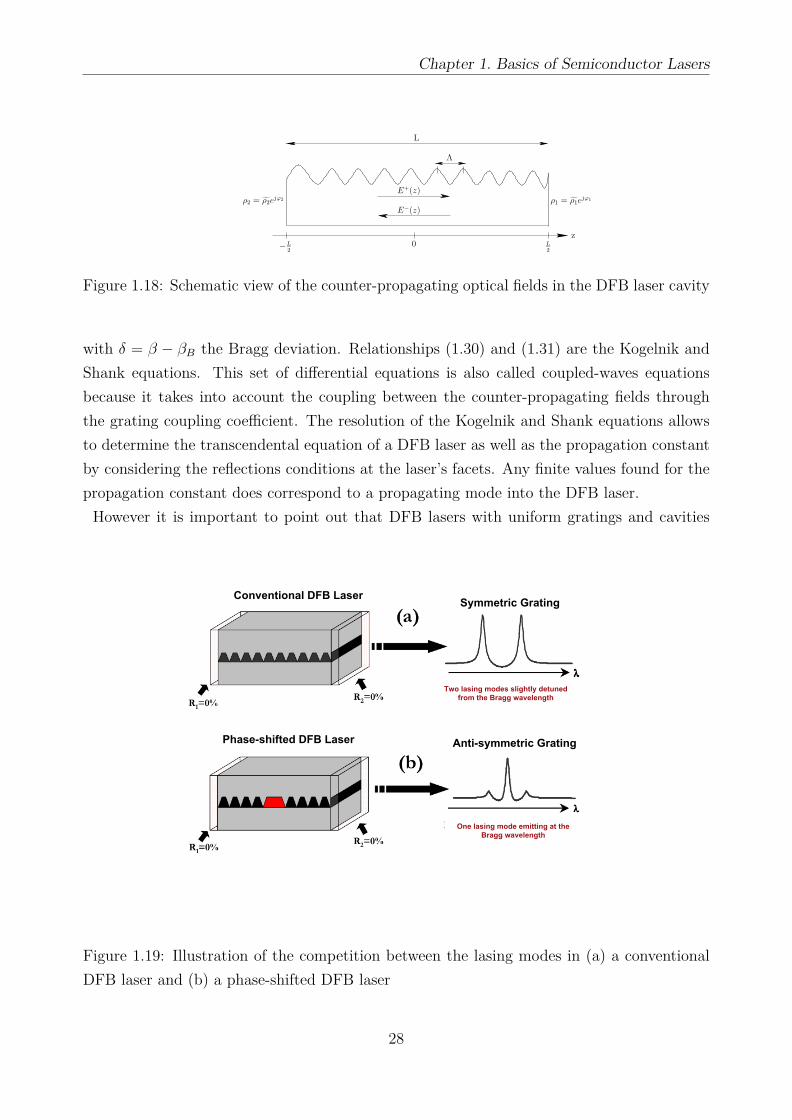
direction is reflected by the grating into a traveling in the opposite direction and vice-versa.In other words, the optical field within the DFB cavity can be written as a superposition ofcounter-propagatives waves such as:
E(z) = E+(z)e−iβBz + E−(z)eiβBz (1.23)
where E+(z) et E−(z) are the electric fields propagative either along the direction +z or−z respectively (see figure 1.18). The Bragg wavevector βB is defined such as βB = 2πn
λB.
26

1.4. Single-Frequency Lasers
Let us stress that the description of the electric field E(z) through (1.23) comes from thetheory of Linear Combinaison of Atomic Orbitals (LCAO). Coherent coupling between thecounter-propagating waves occurs only for wavelengths that satisfy the Bragg condition givenby (1.22). Then, starting from Maxwell’s equations, one can write:
∇× E = −µ0∂H∂t
(1.24)
∇×H = ε(z)∂E∂t
(1.25)
with ∇, E, H, ε(z) and µ0 the Nabla operator, the electric field, the magnetic field, thedielectric permittivity of the material and the magnetic permeability in vacuum. Combiningequations (1.24) et (1.25), the Helmoltz’s equation describing the mode propagation withinthe structure can written such as:
∇2E + β2(z)E = 0 (1.26)
with β(z) the wavevector associated to the propagation of the mode within the DFB cavityand defined as: β(z) = β0
√ε(z)ε0
where (β0 is the wavevector in vacuum and ε0 the dielectricpermittivity in vacuum). The periodic variation induces by the index modulation allows toextract through a first-order approximation both the real and imaginary parts n(z) and α(z)of the effective index:
n(z) = n+ ∆n cos(2βBz) (1.27)
α(z) = α + ∆α cos(2βBz) (1.28)
where n, α the average values of n(z), α(z) and ∆n, ∆α their amplitudes. Thus, based onKramers-Krönig relations and by injecting equations (1.27) et (1.28) into β(z), it comes:
β2(z) = β20n
2 + 2iαβ0n+ 4κβ0n cos(2βBz) (1.29)
where κ = π∆nλ
+ i∆α2 is the grating coupling coefficient . Basically, this coefficient allows to
estimate the strength of the interaction between the optical fields E+(z) and E−(z). Thisparameter is mostly linked to the grating profile, its position from the active region as wellas the thickness and composition of the different layers of the waveguide. Also, it should benoted that the coupling coefficient has a strong impact on the laser’s external optical feedbacksensitivity.Let us now assume the slowly varying envelope conditions, d
2E+,−dz2 � dE+,−
dz. Injecting (1.23)
and (1.29) into (1.26), it comes:
−dE+(z)dz
+ (α− iδ)E+(z) = iκE−(z) (1.30)
dE−(z)dz
+ (α− iδ)E−(z) = iκE+(z) (1.31)
27
Chapter 1. Basics of Semiconductor Lasers
E−(z)
E+(z)
0z
L
L2!L
2
!
ρ1 = ρ̃1ejϕ1ρ2 = ρ̃2ejϕ2
Figure 1.18: Schematic view of the counter-propagating optical fields in the DFB laser cavity
with δ = β − βB the Bragg deviation. Relationships (1.30) and (1.31) are the Kogelnik andShank equations. This set of differential equations is also called coupled-waves equationsbecause it takes into account the coupling between the counter-propagating fields throughthe grating coupling coefficient. The resolution of the Kogelnik and Shank equations allowsto determine the transcendental equation of a DFB laser as well as the propagation constantby considering the reflections conditions at the laser’s facets. Any finite values found for thepropagation constant does correspond to a propagating mode into the DFB laser.However it is important to point out that DFB lasers with uniform gratings and cavities
Active Region Bragg Region
Active Region
Bragg Grating
Conventional DFB Laser
Phase-shifted DFB Laser
Symmetric Grating
Anti-symmetric Grating
Two lasing modes slightly detunedfrom the Bragg wavelength
One lasing mode emitting at theBragg wavelength
Figure 1.19: Illustration of the competition between the lasing modes in (a) a conventionalDFB laser and (b) a phase-shifted DFB laser
28
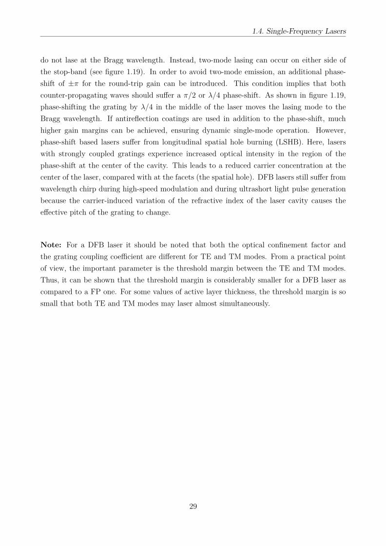
1.4. Single-Frequency Lasers
do not lase at the Bragg wavelength. Instead, two-mode lasing can occur on either side ofthe stop-band (see figure 1.19). In order to avoid two-mode emission, an additional phase-shift of ±π for the round-trip gain can be introduced. This condition implies that bothcounter-propagating waves should suffer a π/2 or λ/4 phase-shift. As shown in figure 1.19,phase-shifting the grating by λ/4 in the middle of the laser moves the lasing mode to theBragg wavelength. If antireflection coatings are used in addition to the phase-shift, muchhigher gain margins can be achieved, ensuring dynamic single-mode operation. However,phase-shift based lasers suffer from longitudinal spatial hole burning (LSHB). Here, laserswith strongly coupled gratings experience increased optical intensity in the region of thephase-shift at the center of the cavity. This leads to a reduced carrier concentration at thecenter of the laser, compared with at the facets (the spatial hole). DFB lasers still suffer fromwavelength chirp during high-speed modulation and during ultrashort light pulse generationbecause the carrier-induced variation of the refractive index of the laser cavity causes theeffective pitch of the grating to change.
Note: For a DFB laser it should be noted that both the optical confinement factor andthe grating coupling coefficient are different for TE and TM modes. From a practical pointof view, the important parameter is the threshold margin between the TE and TM modes.Thus, it can be shown that the threshold margin is considerably smaller for a DFB laser ascompared to a FP one. For some values of active layer thickness, the threshold margin is sosmall that both TE and TM modes may laser almost simultaneously.
29

Chapter 1. Basics of Semiconductor Lasers
30

Chapter 2
Advances in Measurements of PhysicalParameters of Semiconductor Lasers
The fast growing use of semiconductor lasers in various fields including fiber telecommuni-cation systems, optical data storage, remote sensing places very stringent requirements ondevice performance. This requires a detailed understanding of physical processes governingthe behavior of laser diodes. In this review, a broad set of electrical and optical techniques isdescribed which gives complimentary information on the operation of the laser diode. Phys-ical processes below threshold are critical in determining the operating point of the laser.Therefore studying the electrical characteristics and optical emission below laser’s thresh-old is often more informative in the process of understanding the device performance. Someother parameters such as leakage current or wavelength chirp can only be deduced from abovethreshold measurements. Most of the experimental techniques presented in this chapter arein relation to telecommunications lasers. These lasers are usually designed so the outputradiation can be coupled into a the single-mode fiber. These measurements provide criticalexperimental feedback in the process of laser diode optimization.
2.1 Measurements of the Optical Gain
One of the most important parameters relating the physical properties of the semiconductorstructure to output characteristics of the laser diodes is the optical gain. Optical gain and itsdependence on the operating conditions determine not only the basic output characteristics,such as the threshold current, but also the temperature dependence of the output character-istics, as well as high-speed performance of the laser.
31

Chapter 2. Advances in Measurements of Physical Parameters of Semiconductor Lasers
The electric wave in the resonator of semiconductor can be written as:
E = E0(y, z)ej(ωt−kx) (2.1)
where E0(y, z) is the magnitude of the field, and the complex propagation k is:
k(λ) = k′ + jk” = 2πneffλ
− j
2g(λ) (2.2)
with neff the effective index of refraction for the optical mode, and g the modal optical gain.The factor of two comes in because the optical gain is usually defined with respect to opticalpower, not optical field intensity. Modal optical gain g(λ) is related to the material opticalgain G(λ):
g(λ) = ΓG(λ)− αtot (2.3)
where Γ is the optical confinement factor (the fraction of the transverse optical mode overlapping the active layer and therefore experiencing optical gain). The total optical loss αtotconsists of mirror loss and internal loss, usually attributed to free-carrier absorption andscattering from waveguide imperfections:
αtot = αm + αi = 1L
ln(
1√R1R2
)+ αi (2.4)
with R1, R2 the mirror reflectivities and L the cavity length. Let us also stress that theoptical gain is defined in terms of variations such that:
δg = −2δk” = −4πλ
Γδn” (2.5)
2.1.1 Determination of the Optical Gain from the Amplified Spon-taneous Emission
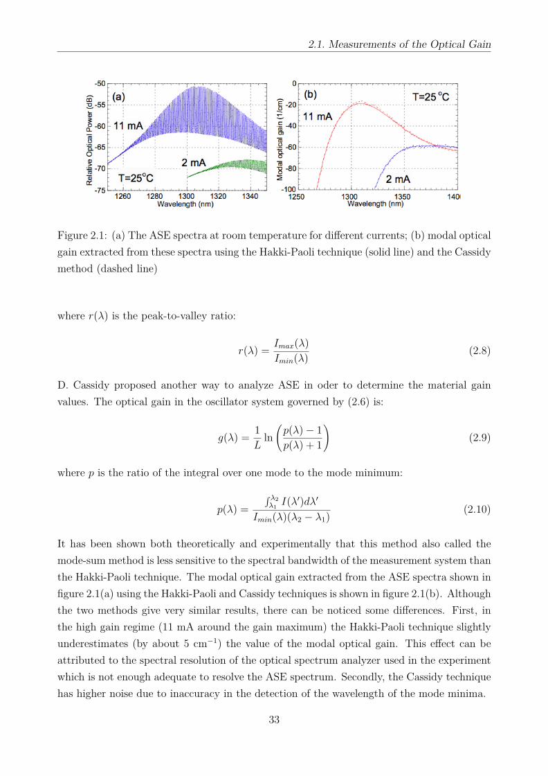
Figure 2.1 shows the spectra of amplified spontaneous emission (ASE) in the TE polarizationfor an 1.3 µm buried heterostructure semiconductor laser with a bulk active region as wellas uncoated mirror facets. The equation describing the dependence of the ASE intensity onthe wavelength in the approximation of uniform gain inside the laser cavity is as follows:
I(λ) = B(1 +Re(ΓG−αi)L)(1−R)(1 +Re(ΓG−αi)L)2 − 4Re(ΓG−αi)L sin2(2πLn
λ)
(2.6)
with R =√R1R2 and B the proportionality coefficient equal to the amount of ASE coupled
into the lasing mode. B. Hakki and T. Paoli proposed to determine the modal optical gainfrom the contrast of the ASE spectra. Equation (2.6) is used to obtain:
g(λ) = 1L
ln√r(λ)− 1√r(λ) + 1
(2.7)
32
2.1. Measurements of the Optical Gain
Figure 2.1: (a) The ASE spectra at room temperature for different currents; (b) modal opticalgain extracted from these spectra using the Hakki-Paoli technique (solid line) and the Cassidymethod (dashed line)
where r(λ) is the peak-to-valley ratio:
r(λ) = Imax(λ)Imin(λ) (2.8)
D. Cassidy proposed another way to analyze ASE in oder to determine the material gainvalues. The optical gain in the oscillator system governed by (2.6) is:
g(λ) = 1L
ln(p(λ)− 1p(λ) + 1
)(2.9)
where p is the ratio of the integral over one mode to the mode minimum:
p(λ) =∫ λ2λ1I(λ′)dλ′
Imin(λ)(λ2 − λ1) (2.10)
It has been shown both theoretically and experimentally that this method also called themode-sum method is less sensitive to the spectral bandwidth of the measurement system thanthe Hakki-Paoli technique. The modal optical gain extracted from the ASE spectra shown infigure 2.1(a) using the Hakki-Paoli and Cassidy techniques is shown in figure 2.1(b). Althoughthe two methods give very similar results, there can be noticed some differences. First, inthe high gain regime (11 mA around the gain maximum) the Hakki-Paoli technique slightlyunderestimates (by about 5 cm−1) the value of the modal optical gain. This effect can beattributed to the spectral resolution of the optical spectrum analyzer used in the experimentwhich is not enough adequate to resolve the ASE spectrum. Secondly, the Cassidy techniquehas higher noise due to inaccuracy in the detection of the wavelength of the mode minima.
33
Chapter 2. Advances in Measurements of Physical Parameters of Semiconductor Lasers
2.1.2 Determination of the Optical Gain from the True Sponta-neous Emission
This method is based on the general relations between the rates of spontaneous emission,stimulated emission and optical absorption. If carriers have a Fermi-like distribution func-tions, the material optical gain is related to the absorption coefficient in the following way:
G(E,EF , T ) = α(E,EF )(eEF−EkT − 1) (2.11)
where E is the photon energy, EF the separation between the quasi-Fermi levels of electronsand holes and α(E,EF ) the absorption coefficient of the material of the active layer. Gener-ally, α(E,EF ) depends on the band filling and therefore on E. Another important relationrelated the intensity of spontaneous emission Isp(E) to the absorption coefficient:
Isp ∝ E2α(E,EF )eEF−EkT (2.12)
where the proportionality sign allows for some constant factors to be omitted. They are ofno importance because it is practically impossible to quantify the absolute measurements ofthe spontaneous. Merging the two previous equations we end-up with:
G(E,EF , T ) = Isp(E)E2 (1− e
E−EFkT ) (2.13)
In order to obtain the value of the material optical gain using (2.13), the value of the quasi-Fermi level separation EF has to be known. Thus, by using the property of a Fabry-Perot laserto lase at the wavelength for which the material gain is maximum, the first derivative withrespect to the wavelength is zero and it gives the value of the quasi-Fermi level separation atthreshold. In oder to determine such values at lower bias currents, it can be shown that at thehigh energies, the absorption coefficient is independent of the injection level. This allows thedetermination of the quasi-Fermi level separation below threshold. It is however important toemphasize that this procedure can lead to serious errors, since the quasi-Fermi level separationhas to be determined with a very high accuracy in order for accurate calculation of the opticalgain from TSE spectra. Attention has also to be paid to the carrier temperature which occursin (2.13); this has to be considered since in the case of carrier heating, the carrier temperatureis not equal to the lattice temperature.One more condition is required to extract the gain spectra from the TSE spectra: equation(2.13) gives the value of the material optical gain in arbitrary units and a proper scaling factorneed to be determined in order to find the material or modal gain. A way is to consider thesituation of Fabry-Perot laser at threshold for which the maximum gain equals the total loss.If the laser has uncoated facets, the mirror loss can be easily calculated. Then, the valueof the total loss can be estimated from the L − I curve slope with an assumption that the
34
2.1. Measurements of the Optical Gain
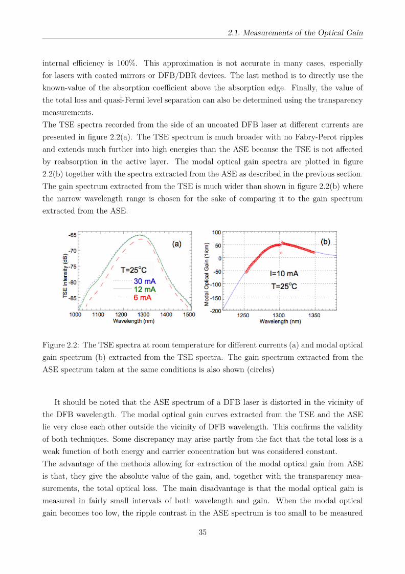
internal efficiency is 100%. This approximation is not accurate in many cases, especiallyfor lasers with coated mirrors or DFB/DBR devices. The last method is to directly use theknown-value of the absorption coefficient above the absorption edge. Finally, the value ofthe total loss and quasi-Fermi level separation can also be determined using the transparencymeasurements.The TSE spectra recorded from the side of an uncoated DFB laser at different currents arepresented in figure 2.2(a). The TSE spectrum is much broader with no Fabry-Perot ripplesand extends much further into high energies than the ASE because the TSE is not affectedby reabsorption in the active layer. The modal optical gain spectra are plotted in figure2.2(b) together with the spectra extracted from the ASE as described in the previous section.The gain spectrum extracted from the TSE is much wider than shown in figure 2.2(b) wherethe narrow wavelength range is chosen for the sake of comparing it to the gain spectrumextracted from the ASE.
Figure 2.2: The TSE spectra at room temperature for different currents (a) and modal opticalgain spectrum (b) extracted from the TSE spectra. The gain spectrum extracted from theASE spectrum taken at the same conditions is also shown (circles)
It should be noted that the ASE spectrum of a DFB laser is distorted in the vicinity ofthe DFB wavelength. The modal optical gain curves extracted from the TSE and the ASElie very close each other outside the vicinity of DFB wavelength. This confirms the validityof both techniques. Some discrepancy may arise partly from the fact that the total loss is aweak function of both energy and carrier concentration but was considered constant.The advantage of the methods allowing for extraction of the modal optical gain from ASEis that, they give the absolute value of the gain, and, together with the transparency mea-surements, the total optical loss. The main disadvantage is that the modal optical gain ismeasured in fairly small intervals of both wavelength and gain. When the modal opticalgain becomes too low, the ripple contrast in the ASE spectrum is too small to be measured
35

Chapter 2. Advances in Measurements of Physical Parameters of Semiconductor Lasers
and analyzed accurately. Measurements based on the TSE spectra are not affected by thevalue or the spectral dependence of the mirror loss or grating. Thus, it can provide the trueinformation about the optical gain in case ASE technique is not suitable. Another advantageis the much wider spectral range of measurements.
2.2 Measurement of the Optical Loss
Internal optical loss is a fundamental characteristics of a semiconductor laser. The valueof internal loss affects threshold current and external slope efficiency. The optical loss hasa number of different contributions; the most important among them are the free-carrierabsorption (intraband process) and scattering loss on the waveguide nonuniformities. Anearly and widely technique for measurement of internal optical loss requires a set of lasers,varying in length but otherwise equivalent, in order to estimate the average value of loss aswell as the internal quantum efficiency. This method does not take into account the systematicvariation of the threshold condition due to variation in length and random variation betweenlasers. Also injection might not be a constant value across the set of different samples dueto incomplete Fermi level pinning resulting from the carrier leakage. As a conclusion, thismethod could not be used only for rough evaluations of optical loss but for the detailedstudies, a more accurate procedure is desirable.Other techniques based on equations (2.3) and (2.4) have been proposed. They are all relatedto the modal optical gain, the material optical gain and the total loss in the laser. From (2.3),it is clear that the modal optical gain equals the total loss (with opposite sign) if the materialoptical gain is zero. This condition holds to good approximation for the energies below thebandgap energy and holds rigorously the transparency energy (at the transition point betweenabsorption and gain). Thus, finding the modal gain at these points provide the value of thetotal loss, which provides the internal loss if the mirror loss is known.A technique based on below-bandgap measurements is made difficult by the low intensity ofthe ASE spectrum in this region. This limits the accuracy of the gain measurements. For thesection spectra shown in figure 2.1(b) the accuracy is no better than 2-5 cm−1. Below bandgaploss measurements are this adequate for rough estimates of loss but become unacceptable formore demanding purposed.Another method to measure internal loss is to determine transparency at a given current so asto find the intersection of the gain curves in TE and TM polarizations under the assumptionthat the optical gain is the same and does not depend on the polarization when the materialgain is zero. Figure 2.3 shows the curves of TE- and TM-polarized-gain measured for a typicalMQW lasers. There is one intersection point at high energy (short wavelength) as well as anindication that the two curves will converge at below-bandgap energies as the material optical
36

2.3. Measurement of the Carrier Leakage in Semiconductor Lasers
gain tends towards zero. The possible source of error with this method is the assumptionthat the total optical loss is equal in the TE and TM polarizations. This may lead to anerror which is in this case of about 2 cm−1.
Figure 2.3: Modal optical gain extracted from ASE spectra of a MQW laser in TE and TMpolarizations
2.3 Measurement of the Carrier Leakage in Semicon-ductor Lasers
Performance of semiconductor lasers depends on heterostructure injection efficiency namelyon the fraction of injected carriers consumed by the active region. One of the mechanisms al-lowing carriers to recombine outside of the active layer is related to the thermoionic emissionof electrons from the active layer to the p-cladding (heterobarrier leakage). Another mech-anism of carrier escaping from active region prior their recombination is lateral transport ofcarriers through the blocking structure or the effect of carrier spreading in broad area lasers.Carrier leakage can affect the laser slope efficiency resulting in its reduction with increasein current and temperature and can also contribute to the temperature dependence of thethreshold current.
2.3.1 Optical Technique of Studying the Carrier Leakage
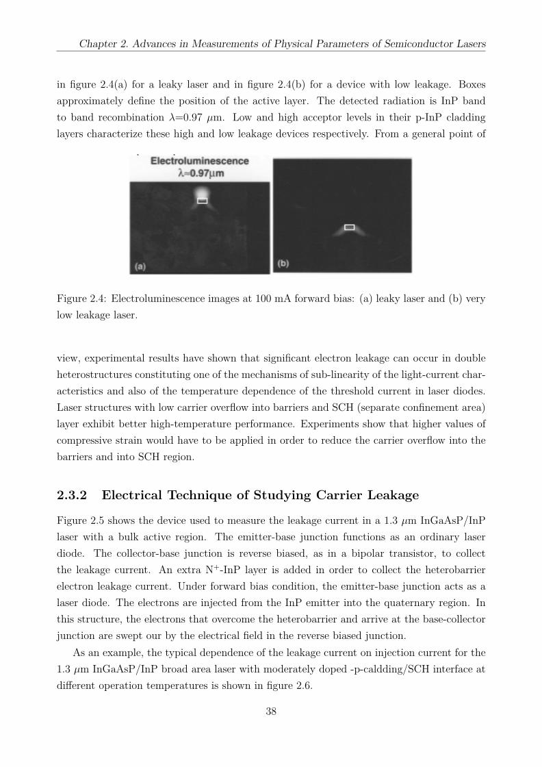
The obvious method of studying the efficiency of carrier leakage under different conditions isto register the light resulting from recombination of carriers outside the active region. For in-stance, electroluminescence image of an InGaAsP/InP laser at 100 mA forward bias is shown
37
Chapter 2. Advances in Measurements of Physical Parameters of Semiconductor Lasers
in figure 2.4(a) for a leaky laser and in figure 2.4(b) for a device with low leakage. Boxesapproximately define the position of the active layer. The detected radiation is InP bandto band recombination λ=0.97 µm. Low and high acceptor levels in their p-InP claddinglayers characterize these high and low leakage devices respectively. From a general point of
Figure 2.4: Electroluminescence images at 100 mA forward bias: (a) leaky laser and (b) verylow leakage laser.
view, experimental results have shown that significant electron leakage can occur in doubleheterostructures constituting one of the mechanisms of sub-linearity of the light-current char-acteristics and also of the temperature dependence of the threshold current in laser diodes.Laser structures with low carrier overflow into barriers and SCH (separate confinement area)layer exhibit better high-temperature performance. Experiments show that higher values ofcompressive strain would have to be applied in order to reduce the carrier overflow into thebarriers and into SCH region.
2.3.2 Electrical Technique of Studying Carrier Leakage
Figure 2.5 shows the device used to measure the leakage current in a 1.3 µm InGaAsP/InPlaser with a bulk active region. The emitter-base junction functions as an ordinary laserdiode. The collector-base junction is reverse biased, as in a bipolar transistor, to collectthe leakage current. An extra N+-InP layer is added in order to collect the heterobarrierelectron leakage current. Under forward bias condition, the emitter-base junction acts as alaser diode. The electrons are injected from the InP emitter into the quaternary region. Inthis structure, the electrons that overcome the heterobarrier and arrive at the base-collectorjunction are swept our by the electrical field in the reverse biased junction.
As an example, the typical dependence of the leakage current on injection current for the1.3 µm InGaAsP/InP broad area laser with moderately doped -p-caldding/SCH interface atdifferent operation temperatures is shown in figure 2.6.
38

2.3. Measurement of the Carrier Leakage in Semiconductor Lasers
Figure 2.5: Schematic representation of the laser-bipolar transistor structure
Figure 2.6: Measured heterobarrier leakage current versus injection current for an 1.3 µmInGaAsP/InP broad area laser
39

Chapter 2. Advances in Measurements of Physical Parameters of Semiconductor Lasers
2.4 Electrical and Optical Measurements of RF Mod-ulation Response below Threshold
Most of the experimental methods aim at determining the carrier concentration which arebased on a model using the balance equations of carriers and photons in the laser. Theseequations also named rate equations can be derived from Maxwell’s equations and are asfollows:
dN
dt= ηint
I
eVact−R− c
neff
dGdN
(N −Nt)1 + εSS
S (2.14)
dS
dt= c
neffΓdGdN
(N −Nt)1 + εSS
S − S
τp− βΓRsp (2.15)
where N and S are the carrier and photon concentrations respectively, I is the pumpingcurrent, e is the electron charge, R the total recombination rate (without the stimulatedemission), Rsp the spontaneous emission rate, c the light velocity in vacuum, neff the effectiverefractive index, G the material optical gain in the active layer, Γ the optical confinementfactor and τp the photon lifetime. Internal efficiency ηint accounts for an imperfect currentinjection efficiency into the active layer. The term (1 + εSS) describes the gain saturationwith photon density, εS being the phenomenological gain compression parameter (related tothe photon density). It was originally introduced to characterize the spectral hole burning.In general this parameter may be used to describe the reduction of the optical gain (linearapproximation) above threshold due to any process, such as spatial hole burning, carrierheating, ...Since the rate equations treat the laser as a medium with single spectral andspatial mode, only the value of the gain at the lasing wavelength is important. Therefore,the wavelength-independent parameter εS can be used. However, the use of this parameter isnot valid when considering the effects that involve gain spectra, since different effects distortthe gain spectra differently and non-uniformly.The first equation describes the balance of the carrier plasma. The carriers are injectedby the injection current (first term), and then recombine spontaneously or non radiatively(second term), as well as through stimulated emission of radiation (last term). The secondequation describes the balance of photons inside the laser cavity. In this set of equations,two important processes are ignored: carrier transport through the SCH and the active layerand carrier capture into quantum wells (in case of QW lasers).The stimulated emission term in the first equation can be neglected below threshold. Then,expressing the recombination in terms of the carrier concentration and carrier lifetime τs:
dN
dt= ηint
I
eVact− N
τs(2.16)
In case of small-signal analysis (small-signal pulse or sinusoidal), the previous equation canbe modified such as:
40

2.4. Electrical and Optical Measurements of RF Modulation Response below Threshold
dδN
dt= ηint
δI
eVact− δN
τs(2.17)
The total number of carriers can be found by integrating the differential carrier lifetime overthe bias current:
N(I) = ηint
∫ I
0τs(I ′)dI ′ (2.18)
Various techniques, based on the relations (2.16), (2.17) and (2.18) have been used to measurethe carrier concentration and the recombination rates in semiconductor lasers. Especially,the carrier lifetime value and its dependence on the current characterize various recombina-tion mechanisms in the active layer of semiconductor lasers. The major mechanism is thespontaneous radiative recombination, a standard bimolecular recombination. Non-radiativeprocesses such as trap or interface and Auger recombination have also been addressed.
2.4.1 Determination of the Carrier Lifetime from the Device Impedance
The equivalent circuit of a semiconductor laser in the small-signal modulation regime belowthreshold is depicted in figure 2.7. It can be derived from the rate equation. The active layeris represented as a RC circuit with characteristic time equal to the differential carrier lifetime.Taking into account a series resistance Rs, introduced by the contacts and cladding layers,
Figure 2.7: Simple equivalent circuit of a laser diode below threshold
and a bonding wire inductance L, the impedance of the equivalent circuit can be writtensuch as:
Z(jω) = jωL+Rs + Rd
1 + jωτd(2.19)
where τd = RdC and Rd is the static differential resistance of the pn junction. This model doesnot take into account the leakage paths and a blocking structure capacitance. It also considersthat transport and capture-escape times are much faster than the differential carrier lifetimeand may be neglected. Equation (2.19) shows that the laser impedance below thresholdis frequency-dependent and that the differential carrier lifetime can be extracted directly
41

Chapter 2. Advances in Measurements of Physical Parameters of Semiconductor Lasers
from electrical measurements of the laser impedance. The laser impedance as function offrequency can be measured using a network analyzer. The real and imaginary parts of thelaser impedance are described by:
Re(Z(ω)) = Rs + Rd
1 + (ωτd)2 (2.20)
Im(Z(ω)) = ωL+ Rd
1 + (ωτd)2 (2.21)
Figure 2.8 shows the real (a) and imaginary (b) parts of the impedance of laser with bulkactive layer at room temperature an current of 1 mA. The solid line are fits to equations(2.20) and (2.21) with the parameter shown. Fitting the real and imaginary parts of the laserimpedance gives very close values for all model parameters. This measurement technique is
Figure 2.8: Measured real (a) and imaginary (b) parts of the laser diode impedance (circles)and fits to equations (2.20) and (2.21) (solid lines)
based on a simple purely electrical measurement. It is useful when optical detection is difficultwhich is the case at low currents and in the wavelength ranges where no fast detectors areavailable. Also, this method is not accurate at high currents, where the value of the differentialresistance Rd gets smaller. This model in general is correct as long as the transport effectsincluding the capture-escape process can be neglected. In the case of highly doped MQWlasers, this model is not accurately correct and a more complicated model is required.Another point to be stressed is that the laser diode may have a parasitic capacitance formedby the contact pads, blocking layers,... In figure 2.7, such a capacitance is connected inparallel with the laser pn junction capacitance. Despite it is usually small compared to thejunction capacitance, the latter one decreasing as the current through the laser decreases,the junction capacitance may become comparable to the parasitic one for certain values ofcurrent.
42

2.4. Electrical and Optical Measurements of RF Modulation Response below Threshold
2.4.2 Determination of the Carrier Lifetime from the Optical Re-sponse Measurements
This technique for determining the differential carrier lifetime proposes to used a small-signalcurrent step excitation. The optical response curve was fitted to an exponential form basedon (2.17). This technique has the disadvantage of high noise if the excitation signal is small.A solution is to use a frequency domain analysis of (2.17) which leads to superior signal-to-noise ratio for the same levels of excitation. Under this assumption, (2.17) has a solution inthe frequency domain:
dδN(ω) = δI(ω)eVact
τd1 + jωτd
(2.22)
where ω=2πf is the modulation frequency and j the complex unit. Under small-signal mod-ulation, the deviation of the photon concentration δS is proportional to the deviation of thecarrier concentration δN . Originally, many authors used the previous equation consideringthat the current amplitude is frequency-independent. However, most of the commerciallyavailable signal generators are power sources, which in the experiment are loaded on the laserdiode. This connection has an equivalent circuit of a voltage source loaded on an r resistorplus a laser impedance Z(jω). The frequency dependence of the impedance results in thefrequency dependence of the amplitude of the current modulation, therefore it should betaken into account in order to correctly extract the value of the differential carrier lifetime.As a consequence (2.22) can be re-written as follows:
dδN(ω) = 1eVact
δV
r + Z(jω)τd
1 + jωτd(2.23)
The voltage modulation amplitude dV (ω) can be considered constant over the frequencyrange. Thus, the knowledge of Z(jω) can be used to correct the measured optical modulationin order to use the single-pole fitting procedure. Using (2.23), one can write:
F (ω) = |δS(ω)||r + Z(ω)| ∝ 1√1 + (ωτd)2
(2.24)
where the corrected function F (ω) can be used to extract the differential carrier lifetime.The measured optical response curve are shown in figure 2.9 (circles) and was corrected using(2.24) (squares) and then fit to a single pole roll-off form from which the differential carrierlifetime can be extracted.
Note: The simplified model of the laser impedance can be used for correction of the differen-tial lifetime data obtained from optical response measurements suiting the values of Rd andRs obtained from either static or dynamic measurements. By substituting equation (2.19)
43

Chapter 2. Advances in Measurements of Physical Parameters of Semiconductor Lasers
Figure 2.9: Optical response curves as measured (circles) and corrected using (2.24) (squares).Lines are single pole fits.
into equation (2.22), a corrected differential carrier lifetime can be obtained:
τd,corr = τd,opt
(1 + Rd
Rs + r
)(2.25)
in which the corrected lifetime is larger than the uncorrected. The use of this simple correctiongives the same value of the differential carrier lifetime as the technique based on impedanceanalysis and impedance corrected optical measurement.
2.5 Optical Measurements of RF Modulation Responseand RIN above threshold
Small-signal response measurement is a very powerful technique that allows analyzing anumber of important device parameters, such as the differential gain and gain suppressioncoefficient. They are also very useful in estimating the device performance in the real operat-ing conditions, such as digital current modulation. Rate equations given by equations (2.14)and (2.15) can be solved for large signal analysis. Also, simple small-signal analysis allowsfor determination of some fundamental characteristics of the laser. Under this assumption,small sinusoidal current modulation around the static value results in sinusoidal modulationof the carrier concentration and photon density:
I(t) = I0 + I1ejωt (2.26)
N(t) = N0 +N1ejωt (2.27)
44
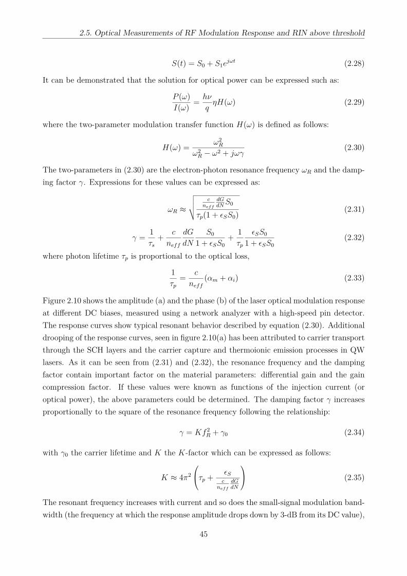
2.5. Optical Measurements of RF Modulation Response and RIN above threshold
S(t) = S0 + S1ejωt (2.28)
It can be demonstrated that the solution for optical power can be expressed such as:
P (ω)I(ω) = hν
qηH(ω) (2.29)
where the two-parameter modulation transfer function H(ω) is defined as follows:
H(ω) = ω2R
ω2R − ω2 + jωγ
(2.30)
The two-parameters in (2.30) are the electron-photon resonance frequency ωR and the damp-ing factor γ. Expressions for these values can be expressed as:
ωR ≈
√√√√ cneff
dGdNS0
τp(1 + εSS0) (2.31)
γ = 1τs
+ c
neff
dG
dN
S0
1 + εSS0+ 1τp
εSS0
1 + εSS0(2.32)
where photon lifetime τp is proportional to the optical loss,
1τp
= c
neff(αm + αi) (2.33)
Figure 2.10 shows the amplitude (a) and the phase (b) of the laser optical modulation responseat different DC biases, measured using a network analyzer with a high-speed pin detector.The response curves show typical resonant behavior described by equation (2.30). Additionaldrooping of the response curves, seen in figure 2.10(a) has been attributed to carrier transportthrough the SCH layers and the carrier capture and thermoionic emission processes in QWlasers. As it can be seen from (2.31) and (2.32), the resonance frequency and the dampingfactor contain important factor on the material parameters: differential gain and the gaincompression factor. If these values were known as functions of the injection current (oroptical power), the above parameters could be determined. The damping factor γ increasesproportionally to the square of the resonance frequency following the relationship:
γ = Kf 2R + γ0 (2.34)
with γ0 the carrier lifetime and K the K-factor which can be expressed as follows:
K ≈ 4π2
τp + εSc
neff
dGdN
(2.35)
The resonant frequency increases with current and so does the small-signal modulation band-width (the frequency at which the response amplitude drops down by 3-dB from its DC value),
45

Chapter 2. Advances in Measurements of Physical Parameters of Semiconductor Lasers
Figure 2.10: Amplitude (a) and Phase (b) of the laser response to small-signal direct currentmodulation
but only up to a certain level. As the DC injection current increases, the response flattens asdepicted in figure 2.10(a). At some point, the damping factor becomes large enough so thatthe modulation response amplitude drops by 3-dB at the frequency below ωR. It was shownthat maximum possible bandwidth is roughly given by,
f3dBmax ≈√
22πK
(2.36)
Note: The knowledge of the dependence of the resonant frequency on current allows de-termining the differential gain in the material of the active layer. Thus, based on (2.30), itcomes:
dG
dN≈ 4π2f 2
Rτpc
neffS0
= 4π2eVc
neffΓηi
(f 2R
I − Ith
)(2.37)
where Ith is the threshold current and the relation between the photon density and the outputpower is such that,
S0 ≈ΓV
Pouthν
(c
neffαm
)−1
= ΓV
ηieτp(I − Ith) (2.38)
where the mirror loss αm is given by the first term of (2.4). In the current treatmentthe effects of the carrier transport and capture into the QW are ignored. More accuratephenomenological treatment yields another factor χ in the right side of (2.37) such thatχ = 1 + τd
τewith τd the carrier capture time including diffusion across SCH and τe the
thermoionic emission lifetime. Differential gain was estimated from the data presented infigure (2.11). Ignoring the transport effects (χ = 1) and assuming the internal efficiency ηiwe find dG
dN≈4.1 10−16 cm2.
Note: The differential gain and the gain saturation parameters can be determined from the
46
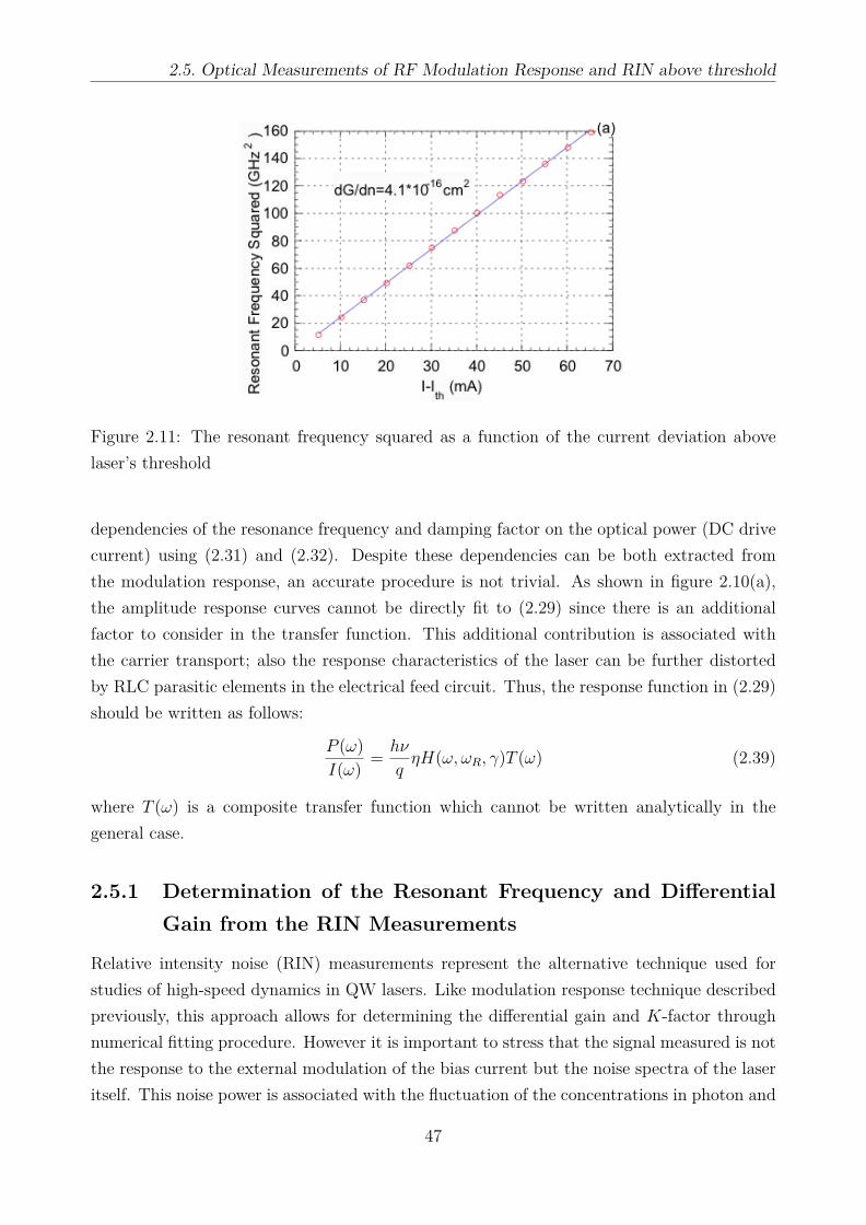
2.5. Optical Measurements of RF Modulation Response and RIN above threshold
Figure 2.11: The resonant frequency squared as a function of the current deviation abovelaser’s threshold
dependencies of the resonance frequency and damping factor on the optical power (DC drivecurrent) using (2.31) and (2.32). Despite these dependencies can be both extracted fromthe modulation response, an accurate procedure is not trivial. As shown in figure 2.10(a),the amplitude response curves cannot be directly fit to (2.29) since there is an additionalfactor to consider in the transfer function. This additional contribution is associated withthe carrier transport; also the response characteristics of the laser can be further distortedby RLC parasitic elements in the electrical feed circuit. Thus, the response function in (2.29)should be written as follows:
P (ω)I(ω) = hν
qηH(ω, ωR, γ)T (ω) (2.39)
where T (ω) is a composite transfer function which cannot be written analytically in thegeneral case.
2.5.1 Determination of the Resonant Frequency and DifferentialGain from the RIN Measurements
Relative intensity noise (RIN) measurements represent the alternative technique used forstudies of high-speed dynamics in QW lasers. Like modulation response technique describedpreviously, this approach allows for determining the differential gain and K-factor throughnumerical fitting procedure. However it is important to stress that the signal measured is notthe response to the external modulation of the bias current but the noise spectra of the laseritself. This noise power is associated with the fluctuation of the concentrations in photon and
47
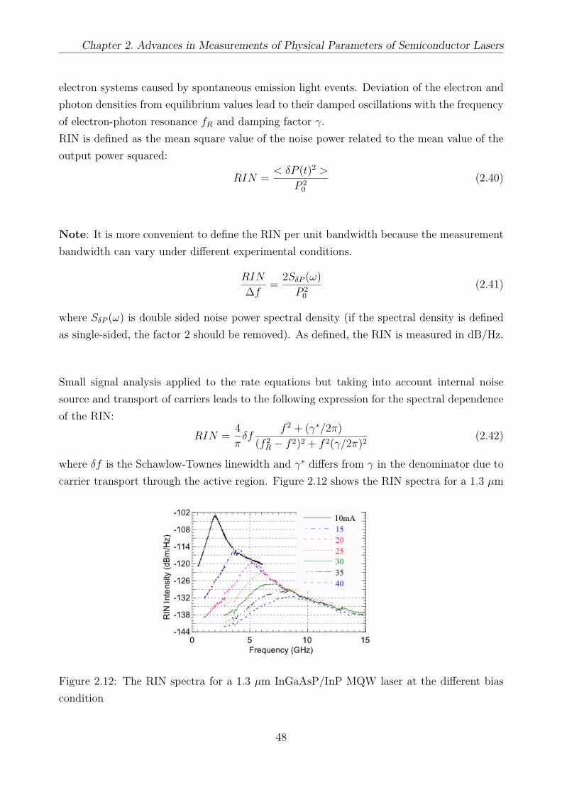
Chapter 2. Advances in Measurements of Physical Parameters of Semiconductor Lasers
electron systems caused by spontaneous emission light events. Deviation of the electron andphoton densities from equilibrium values lead to their damped oscillations with the frequencyof electron-photon resonance fR and damping factor γ.RIN is defined as the mean square value of the noise power related to the mean value of theoutput power squared:
RIN = < δP (t)2 >
P 20
(2.40)
Note: It is more convenient to define the RIN per unit bandwidth because the measurementbandwidth can vary under different experimental conditions.
RIN
∆f = 2SδP (ω)P 2
0(2.41)
where SδP (ω) is double sided noise power spectral density (if the spectral density is definedas single-sided, the factor 2 should be removed). As defined, the RIN is measured in dB/Hz.
Small signal analysis applied to the rate equations but taking into account internal noisesource and transport of carriers leads to the following expression for the spectral dependenceof the RIN:
RIN = 4πδf
f 2 + (γ∗/2π)(f 2R − f 2)2 + f 2(γ/2π)2 (2.42)
where δf is the Schawlow-Townes linewidth and γ∗ differs from γ in the denominator due tocarrier transport through the active region. Figure 2.12 shows the RIN spectra for a 1.3 µm
Figure 2.12: The RIN spectra for a 1.3 µm InGaAsP/InP MQW laser at the different biascondition
48

2.6. Measurements of the linewidth enhancement factor
InGaAsP/InP MQW laser at the different bias condition. The resonance frequency, damp-ing factor and Shawlow-Townes linewidth can be determined from fitting the experimentalspectra with (2.42). Taking into account the carrier transport properties of the structure, thedependence of the resonance frequency on current can be determined. Figure 2.13 shows theexperimental results for the same laser as in figure 2.11. The values of the differential gaindGdN
and of the K-factor are also mentioned. The main advantage of the RIN technique bycomparison with the modulation response one is the elimination of the problem with high fre-quency modulation experimental equipment. Also to be noted is the absence of low-frequencyroll-off in the RIN spectra, which is related to the carrier capture and diffusion across SCH.
Figure 2.13: Determination of the differential gain (a) and K-factor (b) from the slopes ofthe theoretically predicted linear dependencies
2.6 Measurements of the linewidth enhancement factor
The linewidth enhancement factor (LEF), also known as αH-factor, has a great importancefor semiconductor lasers, as it is one of the main features that distinguishes the behavior oflaser diodes with respect to other types of lasers. The αH-factor influences several funda-mental aspects of laser diodes, such as the linewidth, the chirp under current modulation,the mode stability, the occurrence of filamentation in broad-area devices. In synthesis, thedynamics of laser diodes is greatly influenced by the αH-factor, which is of particular in-terest for the study of injection phenomena, optical feedback effects, and mode coupling asoccurring in VCSELs. The birth of the αH-factor traces back to the early 80s, when firstmeasurements revealed that the semiconductor laser linewidth was much broader than whatpredicted by the Shawlow-Townes theory. A theoretical explanation soon came from Henry,who developed a theory that ascribes the excess linewidth to the joint action of spontaneousemission events and population inversion (i.e. carrier) relaxation, through the mechanism of
49
Chapter 2. Advances in Measurements of Physical Parameters of Semiconductor Lasers
index-gain coupling. The latter represents the fact that in a semiconductor medium boththe optical gain and the refractive index depend on the actual carrier density. Since then, anumber of theoretical and experimental works were carried out, with the aim of calculatingthe dependence of the αH-factor on laser diode material parameters, and measuring its valuein practical devices.
2.6.1 Definition
The αH-factor is defined as the ratio of the partial derivatives of the real and complex partsof the complex susceptibility χ = χr + jχi with respect to carrier density N :
αH,T = −∂χr/∂N∂χi/∂N
=
(∂n′
∂N
)T(
∂n′′
∂N
)T
= −4πλ
dn/dN
dg/dN(2.43)
where dn and dg are the small index and optical gain variations that occur for a carrier densityvariation dN . According to the definition, theoretical models describing the optical propertiesof the semiconductor medium were used to numerically evaluate the αH-factor by calculatingthe differential gain and differential refractive index. More accurate models also take intoaccount the effect of free carriers. In a linear approximation, only one among the spectraldependence of the differential gain and differential refractive index shall be calculated, asthe other can be obtained through Kramers-Kronig transformations. Estimated/measuredvalues for αH-factor lie in the range 0.5-8.0, with more common values in the range 2.0-6.0. Typically, αH-factor increases for decreasing photon energy and for increasing carrierdensity. The analysis of different material reveals that, generally, the αH-factor is smaller inMQW than in bulk, and it is even further reduced in strained materials, Quantum Wires andQuantum Dots. Also, novel materials such as InGaNAs/GaAs are very promising for havingαH-factor values around unity. Some authors suggested that non-linear gain and/or carrierheating should have a non negligible effect on αH-factor which in turn should be considered asan optical power dependent parameter (the effective αH-factor should increase with increasingpower). Some authors also attribute the effect of high power linewidth floor/rebroadening tothe power dependence of αH-factor, while others suggested different mechanisms. As a matterof fact, at present no clear experimental and systematic evidence of the power dependence ofthe αH-factor has been reported.
Note: Besides the instantaneous phase change caused by spontaneous emission, there willbe a delayed phase change resulting from the instantaneous change in the field intensity. Torestor the steady-sate field intensity, the laser will undergo relaxation oscillations. During
50

2.6. Measurements of the linewidth enhancement factor
this time, the net gain changes ∆g(t) = −(2ω/c)∆n′′(t) where ∆n′′ is the deviation of theimaginary part of the refractive index from its steady-state value. The change in n′′ iscaused by the modification of the carrier density which also alters the real part n′ of therefractive index. The ratio of this change does correspond to the definition of the linewidthenhancement factor αH = ∆n′/∆n′′. A change in ∆n′ during a limited period of time resultsin an additional phase-shift of the laser’s field and in an additional linewidth broadening.Let us consider a monochromatic wave propagating towards the z direction:
E(ω, z) = E0ej(ωt−kz) (2.44)
with k = ωn/c = ω/c(n′+ jn′′) = k0(n′+ jn′′) the propagation constant. Then injecting into(4.44) it comes,
E(ω, z) = E0ej(ωt−k0n′z)ek0n′′z (2.45)
This relation demonstrates that the real part of the refractive index acts on the electric field’sphase while the real part influences the amplitude. The loss coefficient defined in intensitycam be written such as:
α = −2k0n′′ (2.46)
The power is z-dependent and decays exponentially following the well-known relationshipP (z) = P (0)e−αz. In case of a laser diode the net gain g − α should be used instead:
g − α = −2k0n′′ (2.47)
If g = α, the relative dielectric permittivity is purely real such as εr = n2. If g > α, situationgets different because of the coupling between the refractive index and the carrier density.Thus, considering that the contribution of the imaginary part remains small one can write:
εr = (n′ + jn′′)2 = n′2 − n′′2 + 2jn′n′′ ≈ n′2 + 2jn′n′′ (2.48)
The changes in carrier density will cause n′ and n′′ to deviate from their threshold valuessuch as n′ = n′0 +∆n′ and n′′ = n′′0 +∆n′′. Neglecting the crossing terms and still consideringthat the contribution of the imaginary part is negligible, one obtains:
εr = n′02 +2n′0(∆n′+j∆n′′) = n′0
2 +2jn′0∆n”(
1− j ∆n′∆n′′
)= n′0
2 +2jn′0∆n′′(1+jαH) (2.49)
This last equation points out how occurs the linewidth enhancement factor αH = ∆n′/∆n” inthe relative dielectric permittivity when considering the laser’s situation above the treshold.
51
Chapter 2. Advances in Measurements of Physical Parameters of Semiconductor Lasers
2.6.2 Measurement Techniques of the α-factor
According to the above definition, measurements techniques can broadly be classified as:
1) techniques capable to measure the material linewidth enhancement factor;
2) methods capable to measure the device linewidth enhancement factor.
Methods of class 1 are based on sub-threshold gain/refractive index measurements, and theirresults might not be closely matched to the behavior of lasers in operating conditions. Con-versely, class 2 methods perform the measurement above threshold, and can account for morecomplex effects. Throughout the scientific literature about linewidth enhancement factor, nosystematic comparison of measurement results obtained from different methods on the samedevices has been carried out. Only a few works report the comparison between two methods.It should be pointed out that not all methods are applicable to all types of laser diode de-vices. For example, the common Hakki-Paoli method cannot be applied to VCSELs for theabsence of multiple longitudinal modes, and to date no method has been applied to measurethe αH-factor in Quantum Cascade semiconductor lasers, and only a few reports are availableabout the αH-factor of external cavity semiconductor lasers. It follows here a brief review ofdifferent measurement methods for the linewidth enhancement factor proposed and demon-strated in the scientific literature. For each method advantages and drawbacks are listed,from the point of view of simplicity of the experimental arrangement and accuracy.
ASE-gain spectrum + Fabry-Perot frequency shift (Hakki-Paoli)This technique relies on direct measurement of dg and dn as the carrier density is varied byan unknown amount dN by slightly changing the current of a semiconductor laser in sub-threshold operation. The measurement is performed using a monochromator-based opticalspectrum analyzer. The quantity dn is measured through detection of the frequency shift oflongitudinal Fabry-Perot mode resonances, while dg is obtained via the Hakki-Paoli methodby measuring the fringe contrast (Peak to valley ratio) of the amplified spontaneous emis-sion filtered by the Fabry-Perot cavity. This method is the most common in investigationsabout αH-factor, it is of straightforward implementation, and it can be easily automated viacomputer-controlled procedure. Critical points concern the resolution of the spectrum ana-lyzer for the case of closely spaced longitudinal modes, and the fact that the thermal peakshiftdrift occurring in CW measurements shall be subtracted to reveal the net carrier effect. Thisis a sub-threshold technique, and it only measures the material linewidth enhancement factoras a function of injected current and photon energy (while the exact carrier density must be
52

2.6. Measurements of the linewidth enhancement factor
evaluated by other techniques). Hence, there is no chance to measure the possible dependenceof αH-factor on optical power. It should be noted that this technique and the following oneare the only that allow to measure αH-factor at different photon energies, because methodsin which the laser is operated above threshold only give information about αH-factor at thelasing wavelength. This technique cannot be applied to VCSELs, because these devices haveone single longitudinal mode beneath the useful gain bandwidth. It is also difficult to beapplied to edge-emitting devices with AR-coated facets (such as some DFBs) due to reducedfringe contrast, and to complex-coupled DFBs. The accuracy of the method is generally good(see next paragraph).
Gain spectrum + Kramers-KronigAnother (typically sub-threshold) technique that measures the material linewidth enhance-ment factor as a function of photon energy and injected current is based on accurate gainspectral measurements as a function of the injected carrier density, from which the spectraldifferential gain can be obtained. Subsequently, Kramers-Kronig relations allow to retrievethe differential refractive index and the calculation of αH-factor. The gain spectrum is typi-cally measured from sub-threshold pure spontaneous emission spectra, that must be collectedwithout the effect of cavity amplified spontaneous emission. Hence, light cannot be collectedfrom the output facet of edge-emitting devices, and windows opening must be purposely fab-ricated on the top or the side of devices. Otherwise, direct measurement of the differentialgain can be obtained by ultrafast pump-probe techniques. This method is generally complex,as it involves some experimental difficulties and relevant post-processing of collected data.Its accuracy is moderate (see next paragraph).
LinewidthAccording to Henry theory, the αH-factor directly influences the linewidth of a semiconduc-tor laser, and hence linewidth measurements could give information about αH-factor. Thetheoretical linewidth formula reads:
∆ν = hνvggthnspαm8πP
(1 + α2
H
)+ ∆ν0 (2.50)
where vg is the group velocity, gth is the threshold gain, nsp is the spontaneous emissionfactor, αm is mirror loss, P is the output power per facet, and ∆ν0 is a power-independentlinewidth term. In linewidth methods the semiconductor laser linewidth is typically measuredas function of emitted power, and the slope of ∆ν versus inverse power is used to compute thelinewidth enhancement factor using (2.50). Obviously, the accuracy of this method is greatlyinfluenced by the degree of accuracy that affects the knowledge of other device parameterthat appears in (2.50). In particular, difficult parameters are the spontaneous emission rate
53

Chapter 2. Advances in Measurements of Physical Parameters of Semiconductor Lasers
and the internal loss. Knowledge of the above parameters usually requires a thorough char-acterization of the specific device under test, together with the knowledge of some fabricationparameters (such as facets reflectivities). Hence, this method is hardly applicable to com-mercial semiconductor lasers, or to "black box" devices. This technique has been often usedto measure the αH-factor of VCSELs. The method is of general straightforward implemen-tation, but its accuracy has to be regarded as poor, due to the above mentioned complexdependence of ∆ν on several parameters.
FM/AM modulation This method relies on high-frequency semiconductor laser currentmodulation which, according to theory, generates both amplitude (AM) and optical frequency(FM) modulation. The ratio of the FM over AM components gives a direct measurement ofthe linewidth enhancement factor. The AM term can be measured by direct detection viaa high speed photodiode, while the FM term is related to sidebands intensity that can bemeasured using a high resolution Fabry-Perot filter. This technique allows the measurementof the device αH-factor, it can be applied to all types of semiconductor lasers, and it hasbeen often deployed to characterize VCSELs. The modulation frequency fm must be largerthan the laser relaxation frequency fr, because for fm < fR the FM/AM ratio is frequency-dependent. This fact poses some experimental difficulties for devices with high fr, requiringvery high-speed RF generators and instrumentation. This method is reliable in the hypoth-esis that the susceptibility is linear and the carrier density is longitudinally uniform, andapart from the above mentioned frequency dependence, has a good accuracy. A modifiedmethod is based on the measurement of the chirp of light pulses emitted under large signalmodulation. This technique is useful for assessing the real performance of a semiconductorlaser when application to practical telecommunication system is of importance. However, itsaccuracy for the determination of the αH-factor is only moderate.
A typical experimental setup used for the FM/AM measurement is depicted in figure 2.14. Asstated above, the goal is to determine the characteristics of the frequency modulation (FM)induced by the current modulation in the laser cavity. The signal at the output is analyzedthrough a tunable Mach-Zhender (MZ) interferometer made with two fibered couplers. Thisinterferometer has a free-spectral range (FSR) which is the inverse of the differential delay|T2−T1| between the two arms, T1 and T2 being the propagation time (time delay) in the twoarms respectively. A polarization controller is used to make sure that the two signals locatedat the input of the second coupler have parallel states. Figure 2.14 shows the power at theoutput of the interferometer as a function of the propagation time difference or of the opticalfrequency. In order to finely control the optical path difference, a cylindrical piezoelectrictransducer is used. The transducer located onto of the MZ’s arms is fiber interdependent and
54

2.6. Measurements of the linewidth enhancement factor
directly controlled by an external locking circuit. The system allows to adjust the interfer-ometer on all points of the characteristics. Measurements are done at two different points A
Figure 2.14: The experimental setup used for the determination of AM, FM responses andof the αH-factor
and B, which are in quadrature with each other as shown in the inset of the figure 2.14. Be-cause of the linearity of the MZ interferometer in this region, the FM (or phase modulation(PM)) related to the signal to be analyzed generates an additional amplitude modulation(AM) proportional to the frequency deviation ∆F across the carrier wave. The change ofsign when switching from A to B allows to separate the AM and FM responses as a functionof the modulation frequency fm in the 10KHz to 20GHz range.The signal from a laser under direct modulation can be expressed as follows:
e(t) =√P0 [1 +m cos(2πfmt)]1/2 exp j [2πf0t+ β sin(2πfmt+ φ)] (2.51)
with P0 the average power, m the modulation rate in power (m = ∆P/P0), fm the frequencyof the electrical signal provided by the network analyzer, f0 the central optical frequency,β the modulation rate in frequency such as β = ∆F/fm (∆F being the amplitude of thefrequency modulation across the optical carrier f0) and φ the phase difference between themodulation frequency and the amplitude frequency. As shown in figure 2.14, the networkanalyzer giving two results associated to the A and B operating points respectively, thenormalized measured signals can be expressed as follows,
M± = P0
2 m cos(πfmFSR
)exp(−j2πfmτ)± P0β sin
(πfmFSR
)exp(−j2πfmτ + jφ) (2.52)
55

Chapter 2. Advances in Measurements of Physical Parameters of Semiconductor Lasers
where M+ is the result in A and M− in B respectively while τ is the transit time withinthe interferometer. On one hand, the first term in (2.52) only depends on the amplitudemodulation (i.e β-independent) while the term cos
(πfmFSR
)corresponds to the AM transfer
function of the interferometer. On the other hand, the second term in (2.52) is purely relatedto the modulation frequency (m-independent) and can be expressed as a function of theinterferometer FM transfer function. From equation (2.52), following expressions can bededuced:
2βm
= 1tan
(πfmFSR
) ∣∣∣∣∣M+ −M−M+ +M−
∣∣∣∣∣ (2.53)
φ = arg
(M+ −M−M+ +M−
)(2.54)
Using the definitions of parameters m and β, equation (2.53) allows extracting the chirppower ratio (CPR) such as:
∆F∆P = fm
2P0
1tan
(πfmFSR
) ∣∣∣∣∣M+ −M−M+ +M−
∣∣∣∣∣ (2.55)
The value of the αH-factor is then determined through the so-called relationship,
2βm
= αH
√√√√1 +(fcfm
)2
(2.56)
In equation (2.54), fc is defined as the corner frequency,
fc = 12πvg
∂g
∂PP (2.57)
with vg the group velocity, P the output power and is a nonzero parameter because ofthe phenomenon of nonlinear gain related to nonzero intraband relaxation times as well ascarrier heating. Parameter ∂g/∂P can be expanded as a function of the gain compressionfactor following the relationship,
∂g
∂P= εPg
1 + εPP(2.58)
For typical numbers the corner frequency can be in the hundreds of MHz to few GHz rangedepending on the output power level. On one hand, for modulation frequencies such asfm >> fc which is the case in the experiment since the maximum modulation frequency fmis about 20 GHz range, the factor 2β/m directly equals to the laser’s linewidth enhance-ment factor. On the other hand, for lower modulation frequencies, the ratio 2β/m becomesinversely proportional to the modulation frequency. Let us note that the measurement of2β/m with frequency and at different output power levels could serve for the determinationof the corner frequency and consequently the gain compression factor. Figure 2.15 showsthe ratio FM/AM in amplitude (red) and in phase (blue) as a function of the frequency
56

2.6. Measurements of the linewidth enhancement factor
Figure 2.15: Amplitude and Phase of the FM/AM ratio as a function of the modulationfrequency for the QW DFB laser
Figure 2.16: Ratio 2β/m as a function of the modulation frequency for the QW DFB laser
57
Chapter 2. Advances in Measurements of Physical Parameters of Semiconductor Lasers
modulation for a quantum well DFB laser emitting at 1550 nm. At low frequencies (fm< 10MHz), thermal effects are predominant. The phase between FM and AM reaches 180◦ whenthe modulation frequency keeps decreasing below 10kHz. When 10 MHz < fm < 1 GHz,AM and FM modulations are in-phase (adiabatic regime) and thermal effects are no longersignificant. Then, when fm >1GHz, relaxation oscillation between the carrier and photonnumbers occur leading to a phase difference of 90◦. From the calculations the ratio 2β/m(with β the frequency modulation rate defined as ∆F/fm and m the amplitude modulationrate) can be plotted as a function of the frequency modulation. As shown in figure 2.16the function 2β/m asymptotically tends to the αH − factor. In the figure 2.16, consideringfm >10GHz, the phase of the ratio FM/AM being close to 90◦, the sign of the αH-factor ispositive (a negative phase of -90◦ would mean a negative value of the αH-factor).
Injection LockingInjection of light from a master semiconductor laser into a slave semiconductor laser causeslocking of the slave optical oscillation frequency to that of the master. Typically, the lock-ing region is characterized in terms of the injection level and frequency detuning, showing anasymmetry in frequency due to the non-zero αH-factor. Several methods have been presentedfor the measurement of the αH-factor based on injection locking experiments. These methodsare capable of giving the effective value for αH-factor in operating conditions, and are basedon the complex theory of injection locking dynamics, that can however be simplified to givethe analytic dependence of measurable quantities (such as asymmetric detuning range) onαH-factor. These methods can be divided into two classes:1) methods requiring the measurement of the injection level,2) methods that do not require the knowledge of injection level.An accurate measurement of the effective injection level is generally difficult, because therealways exists a mode profile mismatch between the master beam projected onto the slavelaser facet and the slave guided mode. Such mismatch can reduce the effective injection to avalue that is 10% to 50% of the total facet power. As a consequence, the accuracy of methodsrequiring the measurement of the injection level is poor, while class 1 methods can have agood or moderate accuracy. These techniques are of complicated experimental realization,and have mainly been tested with DFB laser.
Optical FeedbackSimilarly to injection phenomena, the behavior of semiconductor laser subjected to opticalfeedback exhibits some dependence on the actual value of the linewidth enhancement fac-tor, and hence the value can be determined from such experiments. Most of the theoreticalanalysis of the dynamics and properties of semiconductor laser in presence of feedback are
58
2.6. Measurements of the linewidth enhancement factor
based on the Lang-Kobayashi (LK) equations. In early works, experimental observations onsemiconductor laser with optical feedback have been compared to theoretical results, and thelinewidth enhancement factor was used as fitting parameter to achieve agreement betweenexperiment and theory. The determination of the value of the αH-factor was often an addi-tional outcome, as these works were not mainly focussed on this point. Similarly to injectionmethods, the measurement of αH-factor is less accurate where the knowledge of the effectivefeedback level is required. An optical feedback method purposely devoted to the measurementof the αH-factor was presented recently based on the self-mixing interferometry. Accordingto the LK theory, the αH-factor is determined from the measurement of specific parametersof the resulting interferometric waveform, without the need for the measurement of feedbacklevel. Optical feedback methods offer different experimental complexities, depending on thespecific feature of the semiconductor laser subjected to feedback that is measured to determineαH-factor. The measured value for αH-factor is the effective value in operating conditions,and non-linear effects could be revealed at high power. However, this point shall be carefullychecked because non-linearities should possibly be included also in the LK model. As a ruleof thumb, methods requiring the knowledge of the feedback level have a poor accuracy, whilemethods that are independent from this parameter are more accurate.
SOA devicesSemiconductor Optical Amplifiers (SOAs) represent another type of active semiconductordevices that are affected by the non-zero value of the linewidth enhancement factor. Mea-surements of αH-factor in SOAs have been carried out with methods that are similar inprinciple to the Hakki-Paoli technique. SOAs allow for higher injected carrier densities, andhence the αH-factor can be characterized over an extended range of this parameter. Themore accurate technique relies on the measurement of dn via an interferometer that includesthe SOA in one arm, and on dg evaluation via chip gain measurement. The accuracy of thismethod is good, and the results are related to the material αH-factor.
2.6.3 Measurements of linewidth enhancement factor from ASEand TSE spectra
For measuring the linewidth enhancement factor (2.43) can be used with other equationsrelating the change of the real and imaginary parts of the refractive index to the values,which can be measured experimentally. Rewriting (2.5):
δn” = − 1Γδg
4πλ (2.59)
59

Chapter 2. Advances in Measurements of Physical Parameters of Semiconductor Lasers
andΓdn
′
n′≈ dneff
neff= dλ
λ(2.60)
where neff is the effective group index. Substituting (2.59) and (2.60) into (2.43) we get:
αHT = −4πneffλ2
(∂λ
∂g
)T
(2.61)
By recording the ASE at different currents below threshold and measuring the change ofthe gain and the wavelength shift of Fabry-Perot peaks with current one can determinethe linewidth enhancement factor αHT and its dependence on the wavelength and current.Shown in figure 2.17(a) is a set of αHT factor curves measured using the above procedure.This method is now commonly used for measuring the linewidth enhancement factor. Also
Figure 2.17: The linewidth enhancement factor (a) and differential gain (b) versus wavelengthat various bias currents
presented in figure 2.17 are the measured dependencies of linewidth enhancement factor anddifferential gain on the wavelength for various currents. Optimizing the DFB wavelength fromthe data shown in figure 2.17 allowed achieving the small-signal direct modulation bandwidthof 26 GHz and linewidth enhancement factor of near 1. Shown in figure 2.17(b) is the setof the differential gain spectra determined using the below threshold gain spectra combinedwith the carrier lifetime measurements discussed in previous sections. It should be pointedout that the value of the differential gain obtained using this method (indicated by solid circlein figure 2.17(b) is in very good agreement with the value of the differential gain obtained inthe same device from the response measurements described previously.An alternative measurement technique for determination of αHT utilizes the optical gainspectra determined from TSE. Kramers-Krönig relation for small changes of refractive indexis as follows:
δn′ = 2πP∫ +∞
0δn” ε′
ε′2 − ε2dε′ (2.62)
60
2.7. Measurements of the Carrier Temperature and Carrier Heating in Semiconductor Lasers
where P indicates taking the principal part integral. Equation (2.59) can be used to relateδG and δn” :
δn′ = hc
2π2P∫ +∞
0
δG
ε′2 − ε2dε′ (2.63)
The coefficient αT can be determined by substituting (2.63) into (2.43). After some simplealgebra it comes:
αT (ε) =
(∂n′
∂µ
)T(
∂n”∂µ
)T
= 2π
ε′P∫+∞
0 δG(ε′) dε′
ε′2−ε2
δG(ε)T(2.64)
Equation (2.64) allows for determination of αHT from the gain spectrum. In order to performthis procedure, the gain spectra should be obtained in a very broad energy range. However,the commonly used Hakki-Paoli technique for extraction of the gain spectra from amplifiedspontaneous emission (ASE) from the laser facet does not allow for that. Equation (2.64)requires some caution in treating the singularity at ε′ = ε. It should also be noticed, thatthe TSE intensity can be measured in arbitrary units because only the ratio of the integralof the spontaneous emission to its value at certain energy enters (2.64). The ASE measure-ments are usually easier to perform and more accurate, but sometimes the TSE type of themeasurements are the only available solution. Both methods described are based on the be-low threshold measurements, and therefore can give only asymptotic value of the parametersclose to threshold. However they have an advantage, since they can be used to study the de-pendence of the linewidth enhancement factor on carrier concentration and other parametersthat cannot be varied in the real operating conditions above threshold. On the other handthe results of the above threshold measurements remain definitely more accurate since theycan be obtained in the exact operating conditions of the device.
2.7 Measurements of the Carrier Temperature and Car-rier Heating in Semiconductor Lasers
Typical semiconductor lasers operate at the injection current densities of an order of 10kA/cm2 or higher. Under these conditions one can expect a significant difference betweenthe lattice temperature TL and the temperature of the electron-hole-plasma in the active re-gion Te−h. This difference is determined by the power acquired by carriers in the active layerand their energy relaxation time. Since the modal optical gain, wavelength chirp and carrierleakage over the heterobarrier are sensitive to the carrier temperature Te−h, the study ofcarrier heating is important for understanding the laser physics and improving device design.Experimental studies of the heating in heterostructures using optical excitation and time re-solved spectroscopy were carried out. In semiconductor lasers and light-emitting diodes, thecarrier temperature is often estimated from the high-energy tail of the spontaneous emission
61
Chapter 2. Advances in Measurements of Physical Parameters of Semiconductor Lasers
spectra. The problem with the estimation of carrier temperature from the high energy tailof the spontaneous emission arises from the fact that the density of states as well as matrixelement of the optical transition are not well known functions of energy. This makes it diffi-cult to analyze the spontaneous emission. Study of the thermionic emission is also nontrivialsince it requires special sample geometry and is generally unsuitable for real laser structures.An interesting experimental technique allows to measure the rate of change of the carrierplasma temperature with pumping current above threshold. This method is based on therelationship between the rate of carrier heating and the wavelength chirp. Wavelength chirpresults from the dependence of the real part of refractive index on current. The real andimaginary parts of refractive index are related through the Kramers-Krönig relation. Un-der lasing condition the distortion of spectral profile of the optical gain (and therefore theimaginary part of refractive index) is caused by spectral hole burning and carrier heating.However, the experimental studies of fast dynamics of the optical gain in semiconductor laserstructures have shown that the electron-hole plasma thermalization time is much shorter thanthe time needed for thermal equilibrium between the plasma and crystal lattice. Thereforethe carrier heating was considered to be dominant and the spectral hole burning effect wasneglected. In this case the energy distribution of electrons and holes is described by Fermifunctions with the same temperature. This temperature differs from the lattice temperature;also electrons and holes have different quasi Fermi level energies when voltage is applied toa laser diode. Sources of carrier heating above threshold are injection of energetic carriersfrom heterobarriers into active layer and free-carrier absorption. The first effect depends onthe injection current and the second on the optical field. Therefore to first order approxima-tion both effects are proportional to the difference between operating and threshold currents.In a static case above threshold the optical gain is equal to the optical loss. At the lasingwavelength, the reduction of the optical gain due to carrier heating is compensated by of theincrease of the carrier concentration. Expressing this in terms of variations of the imaginarypart of the refractive index yields:(
∂n”∂µ
)T
dµ+(∂n”∂µ
)µ
dT = 0 (2.65)
where µ is the quasi Fermi level separation. However, pinning of the optical gain does notoccur at all wavelengths. The real part of the refractive index is related to the imaginarypart (and optical gain) via the Kramers-Krönig relation. This results in the dependence ofthe refractive index on current above threshold and in the wavelength chirp. The full changeof the real part of the index due to the same small variations dµ and dT , can be expressedin the same terms as in (
∂n′
∂µ
)T
dµ+(∂n′
∂µ
)µ
dT = dn′ (2.66)
62
2.7. Measurements of the Carrier Temperature and Carrier Heating in Semiconductor Lasers
The linewidth enhancement factor as defined in (2.43) can also be defined as a derivativewith respect to the quasi Fermi level separation because only two variables out of three (n,µ and T ) are independent for Fermi-distributed carriers:
αHT =
(∂n′
∂µ
)T(
∂n”∂µ
)T
(2.67)
This definition allows for easier measurement, because quasi Fermi level separation µ is easierto determine than the carrier concentration. The Kramers-Krönig relation suggests that thereis an analogous parameter relating small variations of the real and imaginary parts of therefractive index due to the change of the carrier temperature at a fixed value of the quasiFermi level separation:
αHµ =
(∂n′
∂T
)µ(
∂n”∂T
)µ
(2.68)
It should be noted that unlike αHT , the parameter αHµ could be determined only from TSEmeasurements using a formula similar to (2.64). Determination of this parameter from ASEmeasurements is impossible because the shift of Fabry-Perot peaks with ambient temperatureis determined mainly by the change of the effective index due to the change of the crystallattice temperature, and not the carrier plasma temperature. Combining (2.65) and (2.68)one can relate the change of the real part of the refractive index and change of the carriertemperature:
dn′ = −(αHT − αHµ)(∂n”∂T
)µ
dT (2.69)
Equation (2.69) may be rewritten in terms of laser parameters that can be measured ex-perimentally. Equations (2.59) and (2.60) can be used to express the change of the lasingwavelength due to the change of the carrier temperature in the active layer:
dλ = λ2
4πneff(αHT − αHµ)
(∂g
∂T
)µ
dT (2.70)
Carrier heating lifts the pinned carrier concentration (and quasi Fermi level separation) abovethreshold and results in wavelength chirp. The carrier heating affects the lasing wavelengthin two ways, described by the two terms in brackets (αHT − αHµ) in (2.70). The first termcorresponds to the change of the real part of the refractive index due to change of the quasiFermi level separation. The second term describes the change in real part of the refractiveindex due to the change of the gain profile produced by the carrier heating. To determineaccurately the change of wavelength with current in a small-signal approach, one can use aFabry-Perot etalon method. Rewriting (2.70) for frequency chirp due to current modulation:
dT
dI= 4πneff
(αHT − αHµ)cβ(∂g∂T
)µ
(2.71)
63

Chapter 2. Advances in Measurements of Physical Parameters of Semiconductor Lasers
where β = dν/dI is the chirp parameter. Equation (2.71) establishes the relation between therate of carrier heating above threshold and wavelength chirp. Coefficients
(∂g∂T
)µ, αHT and
αHµ can be determined from the gain measurements described in previous sections. Theirvalues were:
(∂g
∂Te−h
)µ≈-0.45±0.05 cm−1K−1, αHT ≈ 2.1±0.2 and αHµ ≈-1.4±0.3 and β=156
MHz/mA. Using these values, the rate of change of the carrier temperature with current wasestimated to be approximately 0.13K/mA. The accuracy of the estimation is about 25%.This allows for an estimation of the carrier temperature difference between a threshold of15 mA and a typical operating current of 50 mA to be 4.7 K. This is considerably less thanestimated by other studies where the energy relaxation time of the electron-hole plasma wasconsidered to be few picoseconds.
64

Chapter 3
Ultrafast Diode Lasers in Fiber OpticsCommunications
The most important application of ultrafast laser diodes is the field of optical fiber communi-cations. Optical fiber communication systems transmit information through an optical fiberin the form of coded sequences of optical pulses. One of the principal parameters in those sys-tems is the bit rate-distance product which is the product of the number of bits transmittedper second by the repeater spacing. The performance of optical fiber communication systemsdepends on the parameters of the optical fiber (dispersion and loss) and of the laser diode.In particular, the modulation bandwidth of the laser and the spectral purity of the laseremission play a crucial role and affect considerably the the bit rate-distance product. Sincethe minimum loss in conventional silica fibers occurs around 1.55 µm wavelength and thezero-dispersion wavelength is near 1.3 µm, the realization of InGaAsP lasers have attractedattention as the most promising candidates for application in this field.
3.1 High-Speed Modulation of Laser Diodes
The main advantage of semiconductor lasers over lasers of all other types is that they canbe directly modulated by the device current. Thus, direct current modulation results in thesimultaneous amplitude (AM) and frequency (FM) modulations of the laser emission. Thiscomes from the refractive index variations in the laser at the same time when the opticalgain changes as a result of the carrier density variations. The interdependence between AMand FM modulations are governed by the so-called linewidth enhancement factor. In thissection, we will concentrate on concepts of increasing modulation bandwidth as well as ondevice-dependent limitations associated to high-speed operations.
65

Chapter 3. Ultrafast Diode Lasers in Fiber Optics Communications
3.1.1 Small-Signal Modulation Response
Let us consider the dynamic response of the intrinsic semiconductor laser. A considerableamount of information can be obtained by a small-signal analysis of the rate equations thatdescribe the interplay between the carrier density N(t) in the active layer and the photondensity S(t) in the cavity. The laser single-mode rate equations can be written as follows:
dN
dt= I(t)
eV− N(t)
τe− g0(N −Nt)S (3.1)
dS
dt= Γg0(N −Nt)S −
S
τp+ βΓN
τe(3.2)
The small-signal response of the intrinsic laser is obtained by linearizing the rate equationsusing,
N(t) = N0 + δN(t) (3.3)
S(t) = S0 + δS(t) (3.4)
P (t) = P0 + δP (t) (3.5)
I(t) = I0 + δI(t) (3.6)
with N0, S0, P0 et I0 are the steady-state (average) values of carrier, photon densities, powerand current respectively. Small-signal variations are such that δI(t) << I0, δS(t) << S0,δP (t) << P0 and δI(t) << I0. The transfer function for intensity modulation in the frequencydomain is given by:
M(jω) =˜δS(ω)˜δI(ω)
(3.7)
The small-signal solution of the rate equations (3.1) and (3.2) give the intrinsic frequencyresponse Rint =
∣∣∣M(jω)M(0)
∣∣∣ as,Rint = ω4
r
(ω2 − ω2r)
2 + ω2γ2(3.8)
where γ is the damping rate and the undamped resonant frequency ωr is given by the relation,
ω2r = g0S0
τp(3.9)
Figure 3.1 illustrates the general form of the response Rint(ω) for different values of S0. Aresonance in the modulation response at ωr is called the relaxation oscillation and its strengthdepends on the spontaneous emission factor, carrier diffusion and carrier transport effects.Above the resonance peak, the magnitude of the intrinsic response approaches asymptoticallya slope of -40 dB/decade. The parameter f3dB = ω3dB
2π is widely referred to as the modulationbandwidth of the laser. There is a universal relationship between the resonant frequency andthe damping rate. It has been demonstrated both experimentally and theoretically the γ
66

3.1. High-Speed Modulation of Laser Diodes
Figure 3.1: Modulation response of a laser diode for different values of the photon density
varies linearly with f 2r = (ωr2π )2 The proportionality constant is the K-factor of the laser. The
K-factor was originally defined as γ = Kf 2r . However a dc offset is always observed and a
better definition is given by,γ = Kf 2
r + γ0 (3.10)
From this definition and using the small-signal solution of (3.1) and (3.2), the K-factor is asfollows:
K = 4π2τp (3.11)
The K-factor is a figure of merit for high-speed laser diodes since the maximum possibleintrinsic modulation bandwidth fmax (3-dB bandwidth) is determined solely by this factor:
fmax =√
22πK
= 8.88K
(3.12)
This equation clearly shows that the smaller K-factor the better for high-speed operations.The K-factor depends not only on the photon lifetime as described by (3.11) but is signifi-cantly affected by nonlinear gain effects and carrier transport effects as it will discussed later.Typical values of K-factor range from 0.2 to 0.4 ns leading to modulation bandwidths as wideas 20-40 GHz. However, this bandwidth is usually limited by RC parasitics, device heatingand maximum power-handling capability of the laser facets.
How to increase the relaxation frequency and the modulation bandwidth?
- Increasing the photon density S0 via a better confinement of the optical field in the activelayer or by biasing the laser at a higher pump current. The relaxation frequency increases
67
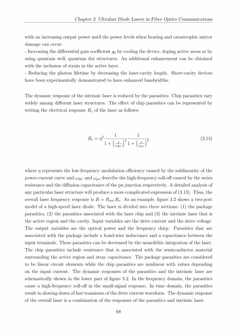
Chapter 3. Ultrafast Diode Lasers in Fiber Optics Communications
with an increasing output power until the power levels when heating and catastrophic mirrordamage can occur.- Increasing the differential gain coefficient g0 by cooling the device, doping active areas or byusing quantum well, quantum dot structures. An additional enhancement can be obtainedwith the inclusion of strain in the active layer.- Reducing the photon lifetime by decreasing the laser-cavity length. Short-cavity deviceshave been experimentally demonstrated to have enhanced bandwidths.
The dynamic response of the intrinsic laser is reduced by the parasitics. Chip parasitics varywidely among different laser structures. The effect of chip parasitics can be represented bywriting the electrical response Re of the laser as follows:
Re = η2 11 +
(ω
ωRC
)21
1 +(
ωωpn
)2 (3.13)
where η represents the low-frequency modulation efficiency caused by the sublinearity of thepower-current curve and ωRC and ωpn describe the high-frequency roll-off caused by the seriesresistance and the diffusion capacitance of the pn junction respectively. A detailed analysis ofany particular laser structure will produce a more complicated expression of (3.13). Thus, theoverall laser frequency response is R = Rint.Re. As an example, figure 3.2 shows a two-portmodel of a high-speed laser diode. The laser is divided into three sections: (1) the packageparasitics, (2) the parasitics associated with the laser chip and (3) the intrinsic laser that isthe active region and the cavity. Input variables are the drive current and the drive voltage.The output variables are the optical power and the frequency chirp. Parasitics that areassociated with the package include a bond-wire inductance and a capacitance between theinput terminals. These parasitics can be decreased by the monolithic integration of the laser.The chip parasitics include resistance that is associated with the semiconductor materialsurrounding the active region and stray capacitance. The package parasitics are consideredto be linear circuit elements while the chip parasitics are nonlinear with values dependingon the input current. The dynamic responses of the parasitics and the intrinsic laser areschematically shown in the lower part of figure 3.2. In the frequency domain, the parasiticscause a high-frequency roll-off in the small-signal response. In time domain, the parasiticsresult in slowing-down of fast transients of the drive current waveform. The dynamic responseof the overall laser is a combination of the responses of the parasitics and intrinsic laser.
68

3.2. Nonlinear Gain Effects
Figure 3.2: A two-port model of a laser diode and schematic of the dynamic response of theparasitics, the intrinsic laser and the overall response of the device
3.2 Nonlinear Gain Effects
3.2.1 Origin and Definition
The dependence of optical gain on the carrier concentration is a relevant approximation ofthe actual gain. However in practice, an additional nonlinear dependence of the gain withthe photon density in the cavity is observed. At high photon densities, the gain is seen tobe reduced or suppressed in comparison to the threshold gain or the gain at low photondensities. A number of physical processes such as the spectral hole burning, spatial holeburning and carrier heating are generally thought to be responsible for gain nonlinearity inlaser diodes. A spectral refers to a slight reduction in gain around the spectral region atthe lasing wavelength due to the finite intraband relaxation time of carriers. At the lasingwavelength, intense stimulated emission depletes electrons and holes faster than the rate atwhich carriers can fill the "hole". The magnitude of the gain compression produced by thiseffect depends critically on the intraband relaxation times. Since these times are typically lessthan 0.1 ps, spectral-hole burning can affect the generation and amplification of picosecondand subpicosecond optical pulses. Recent experiments have also shown that carrier heatingmay also be responsible for nonlinear gain. The fast carrier thermalization maintains electronsand holes in thermal equilibrium with each other at temperatures that are higher than thatof the lattice. The carrier heating is brought about by stimulated emission and free-carrierabsorption. The heated electron-hole plasma loses its energy to the lattice by a combinationof relaxation processes. The higher carrier temperature results in an optical gain suppressionbecause the gain is a sensitive function of carrier temperature. Due to the fact that the
69

Chapter 3. Ultrafast Diode Lasers in Fiber Optics Communications
electron-hole thermalization is a fast process, the dynamic characteristics of laser diodes onpicosecond and subpicosecond time scales must be affected by dynamic carrier heating.An analytical expression of gain, accounting for the effects of photon density is usually writtensuch as:
g(N,S) = g0(N −Nt)(1 + εSS)m (3.14)
with εS the nonlinear gain coefficient (or gain compression coefficient), S the photon densityand m a fitting constant that is often considered as close to the unity or a half. Threeforms of the above general expression are often used in the literature. The first one isg ∝ 1 − εSS for low photon densities and m = 1. It is directly related to the third-ordernonlinear susceptibility of a semiconductor. The second form which is g ∝ (1− εSS)−1 withm = 1, results from a two-level-atom treatment for laser diodes. And finally, the third onegiven by g ∝ (1 − εSS)−1/2 with m = 1/2 is derived from a more rigorous solution using anapproximation for the density of states function.
Note: Because of the quantum confinement of electrons, it can be shown that the nonlineareffects are enhanced in quantum well lasers. QW lasers with thinner quantum-well thicknesshave larger nonlinear gain coefficient at the constant linear bulk gain. By designing thenumber of quantum wells in the laser, it is possible to control the gain nonlinearity. At thelasing condition, the modal gain equals the total loss. The modal gain is defined by the bulkgain multiplied by the optical confinement factor. Since the latter is proportional to thenumber of quantum wells, one can control the carrier concentration (the bulk gain) throughoptimization of the number of quantum wells. Therefore it can be shown that the nonlineargain coefficient becomes larger when decreasing the bulk gain. As a consequence the gainnonlinearity is stronger in multiple quantum well lasers than that in a single quantum welllasers. Thus, the gain nonlinearity is expected to be enhanced in quantum wire and quantumdot based devices.
When nonlinear gain effects are included the relaxation frequency as well as the K-factor ofthe laser are modified. Using the standard rate equations including the gain compressioncoefficient with small-signal analysis, it comes:
ω2r = g0S0
τp(1 + εSS0) (3.15)
and,
K = 4π2(τp + εS
g0
)(3.16)
70

3.2. Nonlinear Gain Effects
Using the nonlinear gain form with m = 1/2, the relaxation frequency and K-Factor aregiven by different expressions: for instance for the resonant frequence, we get:
ω2r = g0S0
τp(1 + εSS0)1/2 (3.17)
The effect of nonlinear gain on the maximum possible modulation 3-dB bandwidth fmax of thelaser is illustrated in figure 3.3. For comparison, the dependence of fmax on εS is calculatedfor two values of differential gain coefficient g0 and two values of τp. Frequency fmax isstrongly dependent on the gain compression coefficient. Nonlinear gain must be consideredwhen ultrafast laser diodes are designed. A characteristic feature of the curves shown infigure 3.3 is that when ε → 0 the maximum modulation bandwidth is primarily determinedby τp whereas for large values of εS, frequency fmax is affected by g0 only.
Figure 3.3: The calculated maximum possible intrinsic modulation bandwidth versus thenonlinear gain coefficient for two values of τp and g0 of 2.4 10−6 cm3 s−1 (dashed lines) and5 10−6 cm3 s−1 (solid lines)
3.2.2 Evaluation of the Gain Compression in Quantum Dot/DashDevices
Measuring the frequency response as a function of the output power is a common method toevaluate gain compression in semiconductor lasers. In the case of the QD laser, effects of gaincompression are more important than those measured on quantum well devices. In order toexplain this phenomenon, a modified nonlinear gain coefficient can be introduced leading to
71

Chapter 3. Ultrafast Diode Lasers in Fiber Optics Communications
a new expression for the relaxation frequency under strong gain saturation such as:
f 2r = vggS
4π2τp (1 + εSS) ≈vgg0S
4π2τp (1 + εS,effS) (3.18)
with vg being the group velocity, g the differential gain, g0 the differential gain at threshold(unsaturated value), S the photon density, τp the photon lifetime, εS the gain compressionfactor related to the photon density and εS,eff the effective gain compression factor definedas follows:
εS,eff = εS1− gth
gmax
(3.19)
where gth is the gain at threshold and gmax is the maximum gain for GS-lasing. Equation(3.19) indicates that the gain compression is enhanced due to gain saturation by a factor ofgmax/(gmax − gth). In Fig. 3.4 the evolution of the normalized gain compression εS,eff/εS isplotted as a function of the ratio gmax/gth. This shows that the higher the ratio gmax/gththe lower the effects of gain compression. If gmax >> gth the graph tends to an asymptotesuch that εS,eff/εS → 1. On the other hand if gmax << gth, gain compression effects arestrengthened: the ratio increases drastically and can even be extremely large if not enoughgain is provided within the structure (gmax ≈ gth). In Fig. 3.5, the square of the measured
Figure 3.4: Normalized compression factor as a function of gmax/gth
resonance frequency is plotted as function of the output power which is linked to the photondensity through the relation with hν the energy per photon, V the cavity volume and αmvgthe energy loss through the mirrors, αm being the mirror loss. The experimental dependenceof the relaxation oscillation frequency shows a deviation from the expected proportionalitygiven by expression (3.18) (case with εS = 0) on the square root of the optical output power Asshown in the inset, a curve-fit based on equation (3.18) is used to express the gain compression
72

3.2. Nonlinear Gain Effects
in terms of a saturation power, Psat ≈ 3.3 mW, where εSS = εPP = P/Psat with εP the gaincompression coefficient related to the output power P . This value means that at this level ofoutput power, non-linear effects start to be significant. Owing to the value of the saturatedpower Psat, the gain compression coefficient related to the output power is estimated to beεP = 1/Psat = 0.3 mW−1. The maximum of the resonance frequency can be directly deducedfrom the curve-fitting as fr = (APsat)1/2 and is expected to be ≈ 5 GHz (not shown in fig.3.5). Taking into account the facet reflectivity as well as the modal volume of the laser, the
Figure 3.5: The square of the resonance frequency versus the output power. The curve-fittingequation is shown in the inset and leads to A=7.5 ± 0.2 (GHz)2 mW−1 and Psat= 3.3 ± 0.3mW.
order of magnitude for the gain compression factor εS is in the range from 5 10−15 cm3 to10−16 cm3. This value remains much larger than those measured on QW lasers (typicallyaround 10−17 cm3).
3.2.3 Consequences on the Linewidth Enhancement Factor
In QW lasers, which are made from a homogeneously broadened gain medium, the carrierdensity and distribution are clamped at threshold. As a result, the change of the αH-factoris due to the decrease of the differential gain from gain compression and can be writtenaccording to the relation:
αH(P ) = αH0(1 + εPP ) (3.20)
where αH0 is the linewidth enhancement factor at threshold. Since the carrier distribution isclamped, αH0 itself does not change as the output power increases. As an example, figure 3.6
73

Chapter 3. Ultrafast Diode Lasers in Fiber Optics Communications
shows the measured linewidth enhancement factor versus the output power for a QW DFBlaser. Black squares correspond to experimental data. As described by equation (3.20), theeffective αH-factor linearly increases with the output power. By curved-fitting those data, theαH-factor at threshold is found to be around 4 while the gain compression coefficient equals3 10−2 mW−1. Compare to QD lasers, such a value of the gain compression coefficient ismuch lower since the enhancement of the effective αH-factor is not significant over the rangeof power. It is worthwhile noting that modifying the laser’s rate equations and including the
Figure 3.6: The effective linewidth enhancement factor as a function of the output power forthe QW DFB laser.
effects of intraband relaxation, the αH-factor can be re-expressed as follows:
αH(P ) = αH0(1 + εPP ) + βεPPεPP + 1εPP + 2 (3.21)
with β the parameter related to the slope of the linear gain which controls the nonlinearphase change. The situation for which β=0 corresponds to an oscillation purely located atthe gain peak. However, second part of (3.21) usually remains small enough to be neglected.
In QD lasers, the carrier density and distribution are not clearly clamped at threshold becausethe inhomogeneous broadening gain is more predominant. Indeed, the lasing wavelength, canswitch from GS to ES as the current injection increases meaning that a carrier accumulationoccurs in the ES even though lasing in the GS is still occurring. The filling of the ESinevitably increases the αH-factor of the GS introducing an additional dependence with theinjected current. Thus taking into account the gain variation at the GS and at the ES, the
74

3.2. Nonlinear Gain Effects
index change at the GS wavelength can be written as follows:
δn =∑
GS,ES
αkδgk (3.22)
with k = GS,ES the indexes of summation for GS and ES respectively. Equation (3.22)leads to:
δn =(αGS + αES
aESaGS
)≡ αHδg (3.23)
In (3.23), δg and δn are the changes of the gain and refractive index at the GS, respectively,αH is the GS-linewidth enhancement factor actually measured in the device, aES and aGS
are the differential gains at the ES and at the GS, respectively, αES describes the change ofthe GS index caused by the ES gain and αGS is related to the GS index change caused bythe GS gain variation. When the laser operates above threshold, αGS keeps increasing withαGS(1+εPP ) as previously shown for the case of QW devices. Let us note that the differentialgain at GS, aGS, can also be simply expressed as a function of the gain compression coefficientas well as gmax and gth. Indeed, it has been shown that the gain saturation in a QD mediacan be described by the following equation:
gGS = gmax(1− e− ln(2)(N/Nt−1)
)(3.24)
with N the carrier density and Ntr the transparency carrier density. When the laser operatesabove threshold, the differential gain for the GS lasing is defined as follows:
aGS = dgGSdN
= ln(2)Nt
(gmax − gGS) (3.25)
with gGS = gth(1 + εPP ) the uncompressed material gain increasing with the output power.Equation (3.25) leads to:
aGS = a0
(1− gth
gmax − gthεPP
)= a0
(1− gth
gmax − gthεSS
)(3.26)
with a0 the differential gain at threshold. Then using equations (3.20), (3.23) and (3.26), thelinewidth enhancement factor can be written as:
αH(P ) = αGS(1 + εPP ) + α1
1− gthgmax−gth
εPP(3.27)
with α1 = αES(aES/a0). The first term in equation (3.27) denotes the gain compression effectat the GS (similar to QWs) while the second is the contribution from the carrier filling in theES that is related to the gain saturation in the GS. For the case of strong gain saturation,(3.27) can be reduced to:
αH(P ) ≈ α1
1− gthgmax−gth
εPP(3.28)
75

Chapter 3. Ultrafast Diode Lasers in Fiber Optics Communications
In figure 3.7, the normalized linewidth enhancement factor αH/α0 is calculated through(3.28) and reported in the (X,Y) plane with X = P/Psat and Y = gmax/gth. This pictureacts as a stability map that simply shows that a larger maximum gain is absolutely requiredfor a lower and stable αH/α0 ratio. For instance let us consider the situation for whichgmax = 3gth: at low output powers i.e, P < Psat, the normalized αH-factor remains constant(αH/α0 ≈ 3) since gain compression is negligible. On the other hand, as soon as the outputpower approaches Psat, and goes beyond, the ratio αH/α0 is increased. Gain compressioneffects lead to an enhancement of the normalized αH-factor, which can go up to 10 forP ≈ 2Psat level of injection for which the ES occurs. On the other hand, assuming gmax = 5gth,
Figure 3.7: Stability map based for the normalized linewidth enhancement factor αH/α0 inthe (P/Psat, gmax/gth) plane
figure 3.7 shows that the effects of gain compression are significantly attenuated since theratio αH/α0 remains almost constant over a wider range of output power. The level at whichgain compression starts being critical is now shifted to P ≈ 3Psat instead of P ≈ Psat. Letus also stress that at a certain level of injection, the normalized GS αH-factor can evenbecome negative. This effect has already been experimentally may occur when the GS gaincollapses, e.g when ES lasing wavelength occurs. In figure 3.8, the calculated GS αH-factor(black dots) of the QD-laser under study is depicted as a function of the bias current. Greystars superimposed correspond to data measurements which have been obtained via theAM/FM technique. This method consists of an interferometric method: the output opticalsignal from the laser operated under small-signal direct modulation is filtered in a 0.2 nmresolution monochromator and sent in a tunable Mach-Zehnder interferometer. From separatemeasurements on opposite slopes of the interferometer transfer function, phase and amplitude
76
3.3. Quantum-Well Lasers and Carrier-Transport Effects
deviations are extracted against the modulating frequency, in the 50 MHz to 20 GHz range.The αH-factor is given by the phase to amplitude responses ratio at the highest frequencies,in the limits of the device modulation bandwidth. Thus, a qualitative agreement between
Figure 3.8: Calculated GS αH-factor versus the bias current (black dots). Superimposedstars correspond to experimental data
simulations and measurements is obtained. As expected, the GS αH-factor increases withthe injected current due to the filling of the excited states as well as carrier filling of thenon-lasing states (higher lying energy levels such as the wetting layer), which results in adifferential gain reduction above threshold. Although the αH-factor is enhanced at loweroutput powers, this increase stays relatively limited until the bias current remains lower than150 mA e.g such that as P < Psat. Beyond that, compression effects starts being significantand the αH-factor reaches a maximum of 57 at 200 mA before collapsing to negative values.As previously mentioned, the collapse in the αH-factor is attributed to the occurrence of theES as well as to the complete filling of the available GS states. In other words, as the ESstimulated emission requires more carriers, it affects the carrier density in the GS, which issignificantly reduced. As a result, the GS αH-factor variations from 57 down to -30 may beexplained through a modification of the carrier dynamics such as the carrier transport timeincluding the capture into the GS. This last parameter affects the modulation properties ofhigh-speed lasers via a modification of the differential gain.
3.3 Quantum-Well Lasers and Carrier-Transport Effects
The use of quantum wells can lead to considerable improvement in the modulation responseof laser diodes mainly due to the enhanced differential gain. Therefore, the higher the differ-
77
Chapter 3. Ultrafast Diode Lasers in Fiber Optics Communications
ential gain, the larger the bandwidth. In contrast to bulk lasers, the differential gain in QWlasers is a structure-dependent parameter; it is determined not only by the material param-eters of the active layer but also influenced by the dimensions of the QW and barrier layers,the optical confinement factor, and the carrier injection and confinement processes. An ac-curate design of the active layer and cladding layers plays a crucial role in the high-speedperformance of QW devices. P-doping of the active layer has been also predicted to enhancethe differential gain and decrease the K-factor of high-speed QW devices. For instance amaximum possible intrinsic bandwidth of 63 GHz (K-factor of 0.14ns) has been reported instrained p-doped InGaAs/GaAs MQW lasers. However, the K-factor and consequently themaximum modulation frequency are affected by nonlinear gain effects that reduce the mod-ulation bandwidth. Because of the inclusion of strain as well as of the quantum confinement,it has been proposed that the gain compression coefficient is enhanced in QW lasers. Despitethe enhanced differential gain, the smallest value of the K-factor observed in these lasers isnot significantly below the best values reported for bulk lasers. Also, there has been a largevariation in the K-factors reported for QW lasers (from 0.13 to 2.4 ns) but for bulk lasers thisparameter has been measured within the relatively narrow range of 0.2 to 0.4ns. The conceptof a well barrier hole burning has been proposed as a possible explanation of this variation.Basically, it consists of an additional contribution to the intrinsic gain compression coefficientwhich is structure-dependent. Another explanation is that carrier transport effects can havea significant impact on the modulation properties via a reduction of the effective differentialgain and not through an enhancement of gain-compression coefficient. This implies that theenhancement of the compression coefficient in QW lasers may not be the primary reason foradditional increase of the K-factor.Unlike the bulk lasers, QW ones have a very small active areas and carrier-tranport effectshas to be considered. This implies that a separate confinement heterostructure (SCH) isnecessary to optimize the transverse optical confinement factor. A SCH layer is inserted be-tween the normally doped cladding regions and the quantum-well active region. A single QWlaser with a SCH is illustrated in figure 3.9. Electron and hole transport from the claddinglayers to the quantum-well active area. Sub-picosecond time-resolved measurements of theluminescence decay in QW structures have shown that the carrier capture time into the QWis roughly 1 ps. Another significant physical mechanism is the thermally activated carrierescape from the QW. This mechanism often called thermoionic emission (associated effectivetime τe) is a strong function of the barrier height. In MQW lasers tunneling effects betweenthe quantum wells may also occur.Rate equations used below describe the dynamics of the carrier densities in the quantum wellNW and the SCH layer NSCH as well as the photon density dynamics in the laser cavity. The
78

3.3. Quantum-Well Lasers and Carrier-Transport Effects
Figure 3.9: Carrier transport in a single separate confinement heterostructure (SCH)
basic equations can be written as follows:
dNSCH
dt= I(t)eVSCH
− NSCH
τtr− NSCH
τn1+ NW
τe
VWVSCH
(3.29)
dNW
dt= −G(NW )S
1 + εSS− NW
τe− NW
τn2+ NSCH
τtr
VSCHVW
(3.30)
dS
dt= ΓG(NW )S
1 + εSS− S
τp+ βΓNW
τn2(3.31)
where VSCH is the volume of the SCH, VW is the volume of the QW, τn1 and τn2 are thecarrier recombination lifetimes in the SCH and active regions, respectively and G(NW ) is thecarrier density-dependent gain. From the small-signal analysis, (3.29), (3.30) and (3.31) andfor negligible τn1 and τn ≡ τn2 one obtains the following analytical approximations for therelaxation frequency and damping rate:
ω2r = (g0/χ)S0
τp(1 + εSS0)
(1 + εS
g0τn
)(3.32)
γ = (g0/χ)S0
(1 + εSS0) + εSS0
τp(1 + εS0) + 1χτn
(3.33)
where the transport factor χ is given by,
χ = 1 + τtrτe
(3.34)
Using (3.32) and (3.33) a relationship for the K-factor can be derived:
K = 4π2(τp + εS
g0/χ
)(3.35)
79

Chapter 3. Ultrafast Diode Lasers in Fiber Optics Communications
For χ = 1 (3.32) and (3.35) transform into (3.15) and (3.16) for the case without carriertransport effect. The first effect of the carrier transport consists of a parasitic-like roll-offin the modulation response that would significantly limit the 3-dB bandwidth for large τtr.This limitation which originates from the finite transport time across the SCH is distinguish-able from the parasitics. The second effect is the reduction of the effective differential gainby a factor of χ. This leads to a reduction of the relaxation frequency for the same powerlevels. The third effect is that the gain compression factor remains unmodified. Figure 3.10illustrates the carrier-transport effects on the maximum possible modulation bandwidth ofa 300-µm QW laser. The dashed line shows the calculated K-factor limit (no carrier trans-port) of the maximum modulation bandwidth as a function of the SCH width. The limitdetermined by the carrier transport model is shown by the solid line. The difference in themaximum possible modulation bandwidth is negligible for the SCH width below 50 nm. How-ever the frequency roll-off due to carrier transport becomes severe for a SCH width largerthan 80 nm.
Figure 3.10: Maximum modulation bandwidth against the SCH width. The dashed lineshows the maximum possible bandwidth without taking into consideration carrier transporteffects
Note: In order to optimize the high-speed performance of QW lasers, the transport timeacross the SCH must be minimized. A narrower SCH should result in a shorter τtr. How-ever decreasing the SCH width below an optimum value will also lead to a drop in theoptical-confinement factor and in an increase of the internal loss. This will result in a higherthreshold carrier density and consequently a lower differential gain originating from rapidgain saturation in QW lasers. Also from (3.34) and (3.35), the thermo-ionic emission lifetimeτe should be maximized. This can be done with deeper and wider quantum wells. However
80
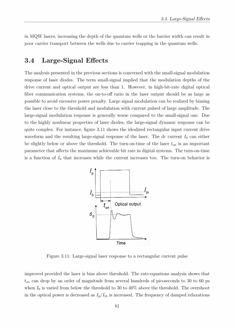
3.4. Large-Signal Effects
in MQW lasers, increasing the depth of the quantum wells or the barrier width can result inpoor carrier transport between the wells due to carrier trapping in the quantum wells.
3.4 Large-Signal Effects
The analysis presented in the previous sections is concerned with the small-signal modulationresponse of laser diodes. The term small-signal implied that the modulation depths of thedrive current and optical output are less than 1. However, in high-bit-rate digital opticalfiber communication systems, the on-to-off ratio in the laser output should be as large aspossible to avoid excessive power penalty. Large signal modulation can be realized by biasingthe laser close to the threshold and modulation with current pulsed of large amplitude. Thelarge-signal modulation response is generally worse compared to the small-signal one. Dueto the highly nonlinear properties of laser diodes, the large-signal dynamic response can bequite complex. For instance, figure 3.11 shows the idealized rectangular input current drivewaveform and the resulting large-signal response of the laser. The dc current I0 can eitherbe slightly below or above the threshold. The turn-on-time of the laser ton is an importantparameter that affects the maximum achievable bit rate in digital systems. The turn-on-timeis a function of I0 that increases while the current increases too. The turn-on behavior is
Figure 3.11: Large-signal laser response to a rectangular current pulse
improved provided the laser is bias above threshold. The rate-equations analysis shows thatton can drop by an order of magnitude from several hundreds of picoseconds to 30 to 60 pswhen I0 is varied from below the threshold to 30 to 40% above the threshold. The overshootin the optical power is decreased as Ip/Ith is increased. The frequency of damped relaxations
81

Chapter 3. Ultrafast Diode Lasers in Fiber Optics Communications
oscillations is roughly equal to the relaxation frequency. The damping is strongly affectedby spontaneous emission that contributed to the laser mode, carrier diffusion and nonlineargain effects.Figure 3.12 shows the simulated optical pulse shapes using the rate-equations for a 1.5-µmlaser diode biased at threshold (I0 = Ith) and modulated at 5 Gbps rate with Ip = Ith for threedifferent values of the saturation parameter p = εSS0 related to the gain compression coeffi-cient, S0 being the steady-state photon density corresponding to an output power of 12 mW.For moderate values of εS (dashed line), the main effect of nonlinear gain is to suppress relax-ation oscillations. For large εS (dotted line), the fall time of the pulse increases considerably.In a communication system, the long trailing edge would even affect the system performancethrough the inter-symbol interference. Gain nonlinearities are thought to set a limit on theon-state power well-below the saturation power level to avoid the detrimental effects of longtrailing edge of optical pulses. As the modulation index of the current modulation is in-creased, novel effects in laser dynamics can be observed. The simplest one is the generationof optical pulses similar to those observed in mode-locked lasers. Directly modulated lasers
Figure 3.12: Effect of nonlinear gain on the large-signal laser response. Optical waveformsare calculated for different values of parameter p = εSS0
can also exhibit a variety of nonlinear dynamic effects including resonance frequency shift,period doubling, period quadrupling and chaos. Some studies have demonstrated that deter-ministic chaos can occur at large modulation index (2 to 4) via period doubling. It has also
82

3.5. Spectral Broadening and Spectral Control Under High-Speed Modulation
been shown that nonlinear gain effects can considerably suppress higher order bifurcationsand the chaotic behavior in directly modulated lasers. In conclusion, these types of irregularbehavior are drastically damaging to applications in optical fiber communication system andhas to be avoided.
3.5 Spectral Broadening and Spectral Control UnderHigh-Speed Modulation
3.5.1 Frequency Chirping
The enhanced linewidth and frequency chirp under the direct current modulation originatefrom variations in the carrier density and from the finite difference in carrier density betweenthe laser on and off states. The chirping response of a diode laser is determined by means ofthe rate equations of the forms (3.1), (3.2) and (3.14) with an additional differential equationthat describes the evolution of the optical phase φ(t) such as:
dφ
dt= 1
2αH(
Γg0(N −Nt)S1 + εSS
− 1τp
)(3.36)
The frequency chirp or chirp is defined as ∆(t) = (1/2π)dφ/dt. Based on (3.36), the chirpcan be directly expressed as a function of the output power:
∆ν(t) = αH4π
(d lnP (t)
dt+ 2ΓεSnP (t)
V ηh̄ω
)(3.37)
where η is the laser differential quantum efficiency. From (3.37) it is clear that the linewidthenhancement factor αH plays a major role in obtaining low-chirp emission from high-speeddirectly modulated lasers. Typical values of αH in most lasers lie in the range from 3 to5. The magnitude of the chirp represented by the first term of (3.37) may be large duringhigh-speed turn-on and turn-off transients but may also be relatively small at the on and offlevels. The second term results in frequency off-set between the on and off levels owing tothe difference in steady-state values of the carrier density. Under digital modulation, whenzeros of the pulse sequence are close to threshold, shoulder can be apparent on both the long-wavelength and short-wavelength sides of the optical spectrum. The former is attributed tothe relaxation oscillations and light present in the trailing edges and nominal zeros of thepulse stream while the latter results from the relaxation oscillations at turn on.
3.5.2 Low-Chirp Lasers
The development of laser structures with αH < 2 has attracted considerable attention. Ac-cording to equation (2.43), this parameter is inversely proportional to the differential gain
83

Chapter 3. Ultrafast Diode Lasers in Fiber Optics Communications
of the laser medium. Since the differential is supposed to be enhanced in QW lasers, theαH-factor has been observed to be reduced in this type of devices. However, the αH-factor isstructure dependent parameter and the effective linewidth enhancement factor αeff should beused in (3.37) for the chirp evaluation. αeff normally exceeds αH . In the case of QW lasers,carrier transport and especially carrier-density variation in the SCH region has a significantimpact on αH-factor and frequency chirping and leads to enhanced values of αeff .
Some achievements to maintain the αH-factor values have been obtained through:- Strained QW lasers usually exhibit reduced αeff -factor. For instance, the αeff -factor of anunstrained MQW DFB lasers was estimated to be 3.1 at 1.55 µm while a similar structurewith a compressive strain had one as low as 1.1.- P-type modulation of QWs has also been demonstrated in order to reduce the αH-factor. Areduction by a factor of two due to modulation doping in both 1.3- and 1.55 µm InGaAsP/InPstrained MQW lasers was observed.- Since the αH-factor depends on the wavelength, the frequency chirp of a laser can be con-trolled by detuning the lasing wavelength with respect to the gain peak. Fabry-Perot lasersnormally lase at the gain peak. However DBR and DFB devices can be tuned to any wave-length as long as the gain peak is positive. This effect is usually to increase the differentialgain in such structures. Figure 3.13 shows the calculated wavelength of the material gain,differential gain and αH-factor of a typical QW laser. As the wavelength is tuned to shorterwavelengths from the material gain peak, the differential gain increases while the αH-factordecreases. The latter becomes even equal to zero in the vicinity of the differential gain peak.Something interesting to stress is that the condition to get αH ≈ 0 lies in the absorptionregion which is the location where the material gain is negative. This means that the wave-length detuning solely cannot result in decreasing αH to zero. The differential gain peak hasto be shifted toward the longer wavelengths in a region where the material gain gets positive.The differential gain spectrum is sensitive to any changes in the valence band structure.Therefore band-structure engineering can offer a number of ways to solve the problem.
3.6 Fundamental Limitations
In this section, some fundamental limitations of multi-gpbs fiber optic digital transmissionsystems exploiting ultra-fast laser diodes are presented. The performance of such systemsappear to be limited by optical power, loss of the fiber, nonlinear effects in both the laserand in the fiber, the spectral bandwidth of the laser emission, the fiber dispersion as well asthe timing jitter.
84

3.6. Fundamental Limitations
Figure 3.13: Calculated dependencies of material gain, differential gain and αH-factor onwavelength in a typical QW laser
3.6.1 Power Limitation
The power available is expressed as the ration of the power launched into the fiber PL andthe minimum power required by the receiver PR to maintain a certain bit-error ration (BER).An optical fiber communication system will be limited by the power to a length such as:
Lmax = PL − PR −Mα
(3.38)
where M is the margin to accommodate, for example, component variations with time andtemperature, α is the fiber loss (in dB/km) and PL, PR are expressed in dBm. The powerlimit can be improved by increasing the power of optical pulses emitted by the laser, byimproving the receiver sensitivity, by improving the laser and fiber coupling efficiencies andby reducing the fiber loss.However increasing the laser power can result in a higher nonlinear gain effects in the laser(limitation of the maximum propagation distance, of the bit error rate,) and in enhancednonlinear propagation of laser pulsed through the fiber. When the power gets higher intothe fiber, it cannot be assumed to behave as a linear transmission medium. The nonlinearrefractive index in the fiber results in self-phase modulation of laser pulsed which in turnleads to the distortion of their temporal profile and optical spectrum. At higher peak powers,transmitted can even break up sub-pulses due to modulational instability in the optical fibers.
85

Chapter 3. Ultrafast Diode Lasers in Fiber Optics Communications
3.6.2 Dispersion Limitation
The dispersion limitation will occur when the pulse spreading causes adjacent pulses tooverlap so that errors result (inter-symbol interference). It is well-known that the pulsewidthincreases with distance due to dispersion. For a system operating at rate B, the dispersionlimited length would be:
LDmax = 12BD∆λ (3.39)
where D is the dispersion parameter of the fiber (in ps/km/nm) and ∆λ is the spectralbandwidth of the laser pulses. The dispersion limit can be improved by reducing the laserchirp by operating at zero-dispersion wavelength of the fiber. The importance of the chirping-induced performance degradation increases with the increase of the transmission bit rate Band can ultimately limit achievable system performance. Penalties in the system due to laserchirping and GVD (Group Velocity Dispersion) effects in the fiber arise because the powerin the initial part of the pulse moves into the previous bit period after a long length of fiber;similarly the power at turn off moves into the following bit interval. The power penalty ina communication system can be analyzed by considering the migration of optical power outof bit interval or by using the eye diagram closure. The power penalty due to laser chirpingcan expressed as follows:
PdB = 10 log( 1
1− 4LBD∆λ
)(3.40)
In order to obtain a low penalty, the laser chirp ∆λ must be minimized. The influence oflinear fiber dispersion may be minimized by operating at the zero dispersion wavelength.However dispersion is not eliminated completely since higher order dispersion terms in fibersare not zero. The second-order GVD results in the asymmetric spreading of an optical pulsegenerating a tail at the trailing edge of the pulse. It was demonstrated that the second-orderGVD may limit the transmission distance at data rates approaching 50 Gbps. At these datarates, the modulation bandwidth is so large that even for ideal transform-limited pulses fiberdispersion significantly broadens the pulses and limits the transmission distance.
3.6.3 Timing Jitter Limitation
The performance of high-speed transmissions are also limited by the pulse timing jitter. Thisjitter may result in power penalties or enhanced BER floors. If the timing jitter is largeenough, additional errors originate from the uncertainty in a pulse position over a significantfraction of the bit period. The origin of the power penalty due to jitter can be explainedthrough the turn-on and turn-off fluctuations of optical pulses. Thus, different portions ofthe received waveform are sampled from bit to bit. Resulting signal fluctuations generateadditional noise and lead to the degradation of the signal-to-noise ratio.. To maintain thesame level of the signal-to-noise ratio, the average received power should be increased. It
86

3.6. Fundamental Limitations
has been shown that the exact amount of jitter-induced power penalty depends on the fiberlength and on the increase of the bit rate B. Calculations have shown that the power penaltyremains small (<0.5dB at the 10−9 BER level) as long as the bit-rate-jitter product BδT isless than 0.06 to 0.15. However for BδT >0.15, the jitter-induced power penalty increasesdramatically up to 10-dB level. A power penalty of 0.7 and 3.2 dB at the 10−9 BER level hasbeen measured for a pseudo-random modulation at a 1.2 Gbps and an rms timing jitter of41 to 60 ps. In addition, the BER performance at the 10−11 level cannot be reached for laserpulses with a rms jitter over 50 ps at the same encoding data. For bit rates greater than 2Gbps, a laser source must have δT below 30 ps to avoid large power penalty.
87

Chapter 3. Ultrafast Diode Lasers in Fiber Optics Communications
88

Chapter 4
Gain and Q-Switching inSemiconductor Lasers
Gain and Q-swtiching of laser diodes by fast switching the optical gain or the intra-cavity lossis a simple technique for producing optical pulses with high repetition rates and high peakpower. Gain switching relies upon the switching of the optical gain through the modulationof the driving current while Q-switching variations of optical loss through passive or activemeans are required. An advantage of gain and Q-swithcing over mode locking is that therepetition rate of output pulses in GHz range can be varied by changing the driving conditions.Also, Q-switching allows the generation of picosecond pulses with peak power that exceedsby a few orders of magnitude that of gain-switched and mode-locked pulses.
4.1 Gain Switching
4.1.1 Principle of Operation
In contrast to mode-locking and Q-switching techniques, gain switching has the advantagethat no external cavity and no sophisticated fabrication technology are required. The idea ofgain switching originated from observations of relaxations oscillations when turning on a laserdiode from below threshold using electrical pulses with a fast leading edge. It was noticedthat the optical pulsewidth was considerably shorter than the electrical pulse. Basically,gain switching consists of exciting the first spike of relaxation oscillation and terminating theelectrical pulse before the onset of the next spikes. It means that the electrical pulsewidthshould be shorter and should lie in the picosecond and nanosecond time range. The generationof ultrashort light pulses by a gain switched diode is illustrated in figure 4.1. The dc bias
89
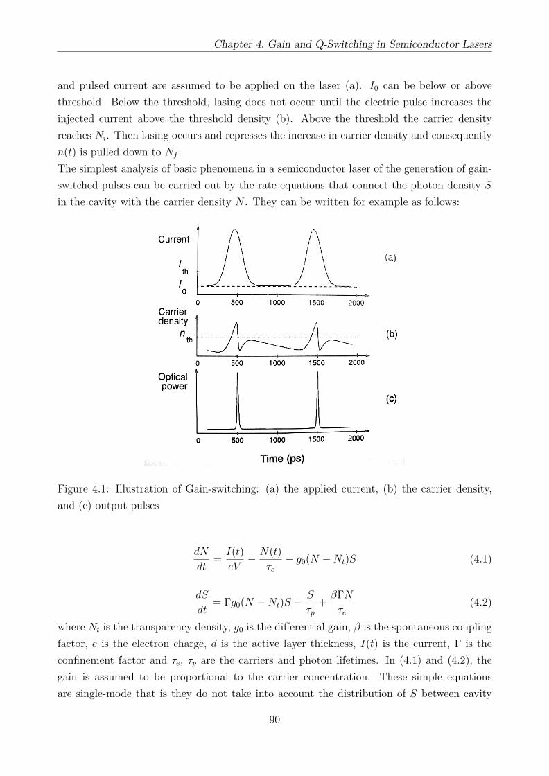
Chapter 4. Gain and Q-Switching in Semiconductor Lasers
and pulsed current are assumed to be applied on the laser (a). I0 can be below or abovethreshold. Below the threshold, lasing does not occur until the electric pulse increases theinjected current above the threshold density (b). Above the threshold the carrier densityreaches Ni. Then lasing occurs and represses the increase in carrier density and consequentlyn(t) is pulled down to Nf .The simplest analysis of basic phenomena in a semiconductor laser of the generation of gain-switched pulses can be carried out by the rate equations that connect the photon density Sin the cavity with the carrier density N . They can be written for example as follows:
Figure 4.1: Illustration of Gain-switching: (a) the applied current, (b) the carrier density,and (c) output pulses
dN
dt= I(t)
eV− N(t)
τe− g0(N −Nt)S (4.1)
dS
dt= Γg0(N −Nt)S −
S
τp+ βΓN
τe(4.2)
where Nt is the transparency density, g0 is the differential gain, β is the spontaneous couplingfactor, e is the electron charge, d is the active layer thickness, I(t) is the current, Γ is theconfinement factor and τe, τp are the carriers and photon lifetimes. In (4.1) and (4.2), thegain is assumed to be proportional to the carrier concentration. These simple equationsare single-mode that is they do not take into account the distribution of S between cavity
90

4.1. Gain Switching
modes. However, they can be easily written for the multimode case. The rate equationsare suitable for the simple treatment of all techniques of generating ultra-short light pulses,including gain and Q-switching as well as mode-locking of laser diodes. For gain-switchingthe current is taken as a train of short electric pulses. For the generation of ultra-short pulses,the differential gain g0 and the photon lifetime τp = 1
vg(αi+αm) (with vg the group velocity, αmand αi the mirror and internal loss) play a significant role.
4.1.2 Pulsewidth and Peak Power
The gain-switched pulse can be described as a combination of two exponential curves withtime constant τr on the rising edge of S(t) and τf on the trailing edge. According to (4.2),for a small enough value of S, gain compression can be neglected and S(t) will increaseexponentially as a result of stimulated emission:
1S
dS
dt= Γg0(N −Nth) = 1
τr(4.3)
The trailing edge of the optical pulse also exhibits an exponential decay constant and normallywe have τf ≈ τr. The FWHM of the pulse can be roughly estimated by the sum τr + τf .The pulse duration is limited by the rate of energy transfer between electron and photonpopulations. Using (4.3) one can deduce that τr ≈ eV
Qg0Γ which means that the risetimeof the pulse is inversely proportional to the net charge Q transferred to the active volumeby the electrical pulse. The decay time τf depends on how far down below threshold thecarrier density is pulled during the optical pulse. One can deduce from (4.3) a correspondingimprovement in the temporal response of gain-switched pulses if the differential gain g0 getslarger. In case of short driving pulses such as I(t) = Niδ(t) with δ(t) the Dirac’s functionand for Ni >> Nth, the pulsewidth of a gain-switched pulse is approximately given by:
∆τ = τp + 1g0Ni
(4.4)
Figure 4.2 illustrates the computer simulation of a typical optical response for a gain-switchedlaser. The main parameter that affects the pulsewidth and the peak power is the initialinversion Ni. It can be shown that Ni depends on the bias current I0 and increases withthe increase of the ratio I1/Ith (with I(t) = I0 + I1 sinωt). The maximum achievable initialinversion is limited by the fundamental parameters of the laser such as the differential gain,the spontaneous emission factor and the cavity loss. It should be noted that when thelaser is driven well above the threshold I1/Ith >> 1 or if electrical pulses are long, multipleoptical pulses are generated within a period of the modulation current. Figure 4.3 shows thecalculated peak power and pulsewidth versus the amplitude of electrical pulses. The CWthreshold current is 20 mA. The maximum value of the ratio I1/Ith is less than 8. Above
91

Chapter 4. Gain and Q-Switching in Semiconductor Lasers
Figure 4.2: Calculated carrier density and photon density against time in a gain-switchedlaser
this value the double-pulse generation occurs. The pulse repetition rate is 1 GHz. It is seenthat the peak power increases while the pulsewidth decreases for higher current amplitudes.A typical pulsewidth lies in the range of 20 to 30 ps.Figure 4.4 shows the parameter of gain-switched pulses a function of the dc bias I0. The
Figure 4.3: Dependence of the peak power and pulsewidth on the amplitude of current pulses.DC bias current is 15 mA. The nonlinear gain coefficient is 0 (solid lines) and 1.5 10−17 cm3
pulse repetition rate is again 1GHz. For a given drive pulse, there is an optimum dc biaslevel for which the FWHM is minimized. This level is below the threshold current. Thus,the difference between the threshold and the optimum bias decreases as the pulsewidth ofelectrical pulses and becomes zero for extremely short driving pulses. This fact is consistent
92

4.1. Gain Switching
with the experiments. When the laser is biased below this optimum level, the pulses broadenand the peak power decreases with the dc bias. At the same time optical pulses are emittedwith progressively longer delay times. It is important to note that both the peak power and
Figure 4.4: Calculated peak power and pulsewidth versus the DC bias. I1 is 100 mA. Thenonlinear gain coefficient is 0 (solid lines) and 1.5 10−17 cm3
the pulsewidth exhibit strong influences of the gain compression. To illustrate this, the peakpower and the pulsewidth are plotted in figure 4.5 versus the non-linear gain coefficient. TheDC bias is 10 mA, the driving current amplitude is 150 mA, and the repetition rate is 1 GHz.The peak power decreases and the pulsewidth increases with the increase of the nonlineargain coefficient. This fact is very important because the nonlinear gain sets the limit for theminimum achievable pulsewidth and the maximum achievable peak power of gain-switchedpulses. Gain-switched pulses can also be improved with the increase of the differential gaincoefficient. Increasing g0 has a twofold effect on the device: first, the pulsewidth decreasesgradually for higher g0; secondly, the peak power increases at the same time. This originatedfrom the fact that initial inversion Ni is higher for higher g0. As a result, QW lasers are morepromising for gain-switching because of their enhanced differential gain as compared to bulklasers.
4.1.3 Optical Spectra and Frequency Chirping
The optical bandwidth of picosecond pulses is a key-parameter for gain-switched lasers. Theanalysis of the generation of the gain-switched lasers was presented via the rate equations fora single-mode laser. However, for gain-switched lasers, many longitudinal modes of the lasercavity may be exited as a consequence of the dynamic overshoot of electron concentration.This can occur even if the laser emission is single-mode under CW operating conditions. InFabry-Perot gain-switched lasers, the optical spectra consists of several (typically 5 to 10)
93

Chapter 4. Gain and Q-Switching in Semiconductor Lasers
Figure 4.5: Dependence of peak power (dashed line) and pulsewidth (solid line) on thenonlinear gain coefficient
longitudinal modes. A typical optical spectrum is shown in figure 4.6: the number of exitedmodes depends on the device structure (index- or gain-guided), the spontaneous emissionfactor, pumping conditions (current amplitudes I0 and I1), and modulation frequency. Whenseveral modes oscillate in the laser, the rate equations (4.1) and (4.2) have to be replaced by:
dN
dt= I(t)
eV− N(t)
τe−∑m
gmSm (4.5)
dSmdt
= ΓgmSm −Smτp
+ βΓNDm
τe(4.6)
where gm = g0(DmN −Nt); Sm is the photon density in the mth laser mode and Dm is thelineshape factor which is defined such as,
Dm = δλ/(π∆λg)1 + [(λm − λ0)/∆λg]2
(4.7)
where δλ is the longitudinal mode spacing, ∆λg is the gain bandwidth, and λ0 and λm arethe wavelengths of the central and mth laser mode. The net photon density equals S(t) =∑m Sm. In addition to multimode operation, the spectral line of each mode is broadened.
If a single-frequency laser diode is used for gain-switching, the multimode operation canbe avoided. However the bandwidth under gain-switching usually exceeds the bandwidthunder CW operating conditions as shown in figure 4.6. The time dependence of the laserwavelength is related to the time dependence of the carrier concentration due to the effectsof free-carriers on the refractive index of the semiconductor material. The instantaneouswavelength is related to the refractive index as:
λ(t) = n(t)n0
λ0 (4.8)
94

4.1. Gain Switching
Figure 4.6: Typical spectra of (a) a FP gain-switched laser and (b) a single-mode laser undergain switching (solid line) and under CW operating conditions
where n(t) and n0 are the refractive indices at times t and 0. Free-carrier plasma refraction,band-gap shrinkage and the dynamic Burstein-Moss shift (modification of the interbandabsorption from free carriers at high doping levels) are the principal mechanisms by whichthe carrier concentration affects the refractive index. Although carrier-induced refractiveindex changes depend on a number of factors, and the exact expression of n as a function ofcarrier density is very complicated, one can write for simplicity,
n(t) ≈ dn
dNN(t) (4.9)
A typical value of dn/dN is -2-3 10−20 cm3 for InGaAsP lasers. Combining (4.8) and (4.9)one obtains for the wavelength chirp ∆λ during the gain-switched pulse,
∆λ ≈ dn
dN
λ0
n0∆N(t) (4.10)
with ∆N = Ni−Nf . Because dn/dN < 0, the wavelength shifts towards longer wavelengths(red-shift). In accordant with (4.10), the estimated linewidth broadening for gain-switchedpulses is typically 0.2-0.3 nm.Due to the wavelength chirp, gain-switched pulses have a time-bandwidth product ∆τ∆νthat is normally far from the theoretical limit for bandwidth-limited pulses. Thus, the time-bandwidth product of optical pulses is given by,
∆τ∆ν = K(1 + α2H)1/2 (4.11)
with αH the linewidth enhancement factor (see chapter 2) andK the constant that is differentfor different pulse shapes. The wavelength chirp has been found to increase when the optical
95

Chapter 4. Gain and Q-Switching in Semiconductor Lasers
pulsewidth decreases in gain-switched lasers. Computer simulations of the laser dynamicsindicate that there is an optimum electrical pulse duration (≈150 ps) for which the product∆τ∆ν has a minimum value. Since the frequency chirp results from variations of the carrierdensity, it is observed both in single-frequency and multimodes lasers. The chirping depend-ing on the modulation of the carrier density spatially averaged over the optical mode, it isexpected that the chirp varies significantly in different laser structures (gain- or index-guidedfor instance). A good spatial overlap of the optical mode and the carrier density is expectedto reduce the frequency chirping.
4.2 Q-Switching in Laser Diodes
4.2.1 Active Q-Switching
Actively Q-switched is not widely used as both gain-switched and mode-locked lasers. Theintracavity loss is modulated electrically or optically in a laser under active Q-switching. Atypical actively Q-switched laser diode is a multiple contact laser, and it often consists oftwo or three sections (a gain section, a modulator section, and a passive waveguide sectionin-between). Since the modulator section and the gain section are fabricated monolithcallyand have exactly the same material composition, the band-gap in the gain section must beshifted to lower energies to prevent band-to-band absorption and to increase the modulationeffectiveness. The time evolution of loss, inversion and optical pulses in an actively Q-switchedlaser is depicted in figure 4.7. The modulation of loss is realized by shifting the band edge inthe modulator section using the Franz-Keldysh effect or the quantum confined Stark effectin MQW lasers that is caused by the applied electric field.
Note: When an electric field is applied, the electron and hole wavefunctions become Airyfunctions rather than plane waves. The Airy function includes a tail which extends into theclassically-forbidden band gap. According to Fermi’s Golden Rule, the more overlap there isbetween the wavefunctions of a free electron and a hole, the stronger the optical absorptionwill be. The Airy tails slightly overlap even if the electron and hole are at slightly differentpotentials (slightly different physical locations along the field). The absorption spectrum nowincludes a tail at energies below the band gap and some oscillations above it. This explanationdoes, however, omit the effects of excitons, which may dominate optical properties near theband gap. The Franz-Keldysh effect occurs in uniform, bulk semiconductors, unlike thequantum confined Stark effect, which requires a quantum well.The absorption spectrum of MQW exhibits an enhanced absorption at the band edge. This iscaused by excitons whose binding energy is enhanced by the carrier confinement. The exciton
96

4.2. Q-Switching in Laser Diodes
absorption peak shifts to lower energies when an electric field is applied to the quantumwells. This effect is much larger than the Franz-Keldysh effect in bulk materials. It can
Figure 4.7: Active Q-switching: evolution of loss/gain, carrier density, and optical power. Ni
is the initial carrier density just before the pulse emission
be shown that the Q-switched pulse parameters are drastically dependent on the photonlifetime τp and on the initial inversion level Ni. One can deduce this by considering therate equations (4.1) and (4.2). When the ultrashort pulse is emitted, stimulated emission isthe dominant mechanism and the contribution of all other processes, including spontaneousemission, carrier pumping and recombination are negligible. Thus, based on rate equationsthe relation between carrier and photon densities in the laser cavity can be written such as:
S(t) = Ni −N(t)− [1/(g0τp)]− ln[(Ni −Nt)/(N(t)−Nt)] (4.12)
Introducing the inversion r and the energy extraction efficiency η, the peak power of theQ-switched pulse is given by,
S0 =(
1g0τp
)(r − 1− ln r) (4.13)
The pulsewidth of the pulse is,τQ = rητp
(r − 1− ln r) (4.14)
Equations (4.13) and (4.14) show that to get shorter pulses, the initial inversion should behigher whereas the photon lifetime should be lower. For instamce for r = 1.1, the pulsewidthτQ is about 50τp and τQ ≈ 5τp for r = 2.0. Also, it is important to stress that high-poweractively Q-switched laser diode can suffer from gain compression via an asymmetry in thepulse shape. Values of τQ in the range of 20 to 60 ps can be obtained.
97

Chapter 4. Gain and Q-Switching in Semiconductor Lasers
4.2.2 Passive Q-Switching
Passive Q-switching is one of the simplest techniques for generating picosecond pulses in laserdiodes. Similar to actively Q-switched, passively Q-switched lasers are always multi-contactdiodes. A saturable absorber located in the laser cavity is responsible for the generation ofutrashort pulses in such devices. The fundamental difference between the two techniques isthat as compared to active Q-switching no external electrical or optical modulation is requiredto produce ultrashort optical pulses. In the case of active Q-switching, the pulse repetitionfrequency is set by an external RF or optical signal, whereas for passive Q-switching, thefrequency is governed by the laser parameters and pumping conditions. The action of asaturable absorber is depicted in figure 4.8. As a result of the nonlinear transmission char-acteristics of the absorber, the initial amplitude distribution of the light is distorted whena light beam is passed through it. The passage of a light pulse leads to a pulse shaping, asshown in figure 4.8. The absorption of the leading edge of the pulse is increased as comparedwith the trailing one. This results in the pulse shortening and leads to generation of asym-metric pulses. The unpumped segments of a laser diode or sections with a low pumping rate
Figure 4.8: Typical transmission characteristic of a saturable absorber an illustration of thepulse shaping by the absorber
in a multiple-contact laser act as a saturable absorber. To generate self-sustained pulsationsor self-Q-switched pulses, the saturable absorber in the laser cavity must satisfy a numberof conditions. The most important parameters that affect the dynamic behavior of the laserare the ratio of the differential loss da/dN of the absorber to the differential gain dg/dN of
98

4.2. Q-Switching in Laser Diodes
the amplifier section and the ratio of the carrier lifetime in the gain τg and the absorber τasections. It can be shown that the following conditions are required for the generation ofQ-switched ultrashort optical pulses:
da/dN
dg/dN> 1 (4.15)
and,τaτg> 1 (4.16)
Owing to specific dependence of gain/absorption on the carrier concentration, the values ofda/dN and dg/dN can be controlled by using different current input applied to differentsections of the laser. As a result, the pulsewidth, the peak power and the repetition rateare dependent on the driving current. Ranges of parameters da/dN , dg/dN , τg and τa canbe calculated using the simple rate equations. In early experimental studies, relatively long30- to 100 ps pulses at repetition rate up to 3 to 5 GHz were generated with passively Q-switched lasers. Typical values of pulse peak power are in the range from 0.1 to 1W. Thepulse parameters are dependent on the photon lifetime τp and the absorber recovery rateon carrier lifetime τa. The recovery of the absorber is due to spontaneous recombinationof excited electron-hole pairs. Let us note that the location of the absorber section at themiddle between the gain regions and the application of the reverse bias on the absorber allowsto improve the pulse parameters that are generated by three-section lasers as compared tothe two-section ones. This improvement can be explained by a significant decrease in theabsorber recovery time.
4.2.3 Optical Spectra
Similar to gain-switched lasers, many longitudinal modes of a laser diode cavity may be ex-cited in Q-Switched lasers as a consequence of the dynamic overshoot of electron concentrationand the variation of carrier density during the emission of optical pulses. In Fabry-Perot self-Q-switched lasers, typical optical spectra consist of several longitudinal modes. A typicaloptical spectrum of a Q-switched Fabry-Perot laser is very similar to that of a gain-switchedlaser. Self-Q-switched lasers normally have a spectral bandwidth as wide as 3 to 5 nm andgenerate picosecond pulses with a time-bandwidth product ∆τ∆ν that exceeds by severaltimes that for bandwidth limited pulses.To reduce the spectral bandwidth of Q-switched pulses, single-frequency lasers (includingDFB and DBR) should be used. The generation of bandwidth-limited high-power Q-switchedpulses was reported using a multi-sections DFB InGaAsP lasers. The optical spectrum of Q-switched pulses is shown in figure 4.9. The lasing wavelength is 1503 nm and the bandwidth
99

Chapter 4. Gain and Q-Switching in Semiconductor Lasers
is roughly 0.18 nm (FWHM). The wavelength of Q-switched pulses was shifted by approxi-matively 2 nm to achieve a shorter wavelength as compared to the wavelength under the CWoperation of the same device. The spectrum exhibits an asymmetric shape with a residualtail to shorter wavelengths. Both temporal and spectral shapes of Q-switched pulses are verysimilar to those of gain-switched pulses generated with multi-sections DFB lasers. The timebandwidth product was measured to be 0.24. Taking into account the experimental error,this value agrees with the time-bandwidth product for Fourier-limited asymmetric pulses.
Figure 4.9: Typical optical spectrum of a Q-switched multi-section DFB laser
100

Chapter 5
Mode-Locked Semiconductor Lasers
The basic advantage of mode locking is that it generates much shorter pulses as comparedto gain or Q-switching. Mode-locking can be realized using a number of techniques mostlyincluding active, passive and hybrid methods. A laser runs at wavelengths dictated by twomajor factors. The first is the bandwidth of the gain medium, and the second is the wave-length range dictated by the cavity is not continuous, it is divided up into cavity modeswhere the spacing between each mode is determined by the cavity length. A single-modelaser will lase on only one of these longitudinal cavity modes while a multimode laser oper-ates on multiple cavity modes. If the phase between each cavity mode is not well-defined,then the output of the laser will be continuous and noisy. If it lases on an enormous numberof modes, then trough averaging it becomes quiet again. The process of mode-locking definesthe phase between each mode. Mode-locking is achieved by changing the Q-factor of thecavity periodically at a harmonic of the frequency determined by the roundtrip time of thecavity (mode-spacing). This periodic change of the cavity Q can be accomplished either bypassive or active means and causes the laser output to be pulsed at the roundtrip time of thecavity. In the case of active mode-locking, an optical device is placed in the cavity whose thetransmission can be rapidly modulated through external electronics. Passive mode-lockingschemes are accomplished by placing a material with non-linear response in the cavity. Thismaterial can be a saturable absorber, or it can exhibit a nonlinearity that changes the in-tracavity propagation properties of the beam (Kerr Lens mode-locking). Thus, the laserwill naturally begin to output pulses when all of the modes are in phase and constructivelyinterfere to produce pulses.
101

Chapter 5. Mode-Locked Semiconductor Lasers
5.1 Principle of Operation
The generation of ultrashort pulses is based on the confinement of the energy in a laser cavityinto a small spatial region. The laser emission consists of a set of resonator modes ωm (withm=1,2,3,...) separated by δω. The number of modes that oscillate is limited by the spectralbandwidth ∆ωg over which the gain exceeds the cavity loss. The output can be seen as asum of frequency components that correspond to oscillating modes. The electric field can bewritten such as:
E(t) =∑m
Am exp j[(ω0 +mδω)t+ Φm] (5.1)
Equation (5.1) does not consider the spatial distribution of the electrical field. The amplitudeand the phase of the mth mode are denoted Am and Φm respectively. In general, relativephases between the modes are randomly fluctuating. If nothing fixes the phase Φm, the laseroutput will vary randomly in time, the average power being approximatively equal to thesimultaneous one. However, if the modes are forced to maintain a fixed phase and amplituderelationship
Φm − Φm−1 = δΦ (5.2)
AmejΦm = A0e
j(Φ0+mδΦ) (5.3)
then the output of the laser will be a periodic function of time:
E(t) = A0
(sin[(k + 1)δωt1/2]
sin[δωt1/2]
)eiω0t (5.4)
where k is the number of locked modes and t1 = t+δΦ/δω. Figure 5.1 illustrates the envelopeE2(t) for k=10. The operating conditions given in the equations written above result in thegeneration of a train of regularly spaced optical pulses. This dynamic regime is named mode-locking. The pulses have a width ∆τ which is proportional to 1/∆ωg. The pulse train hasa periodicity of T = 2nL/c. The ratio of the period T to the pulsewidth ∆τ is equal to thenumber of locked modes k.
5.2 Active Mode-Locking
Active-mode locking is achieved by modulating the loss or gain of a laser diode at a frequencythat is equal to the inter-modal spacing δν. In this case, each spectral mode is driven bythe modulation sidebands of its neighbors. Thus, phases of modes are locked by the externalmodulation. Active mode-locking is schematically illustrated in figure 5.2. The modulation ofthe gain in the laser at the intermodal spacing frequency results either from modulating thedriving current or using an external modulator. Sine wave oscillators are normally used for thecurrent modulation. Alternatively ultrashort electrical pulses from a comb generator can be
102

5.2. Active Mode-Locking
Figure 5.1: Ideal mode-locking: the output of a laser with 10 completely locked modes
used. The modulation is often superimposed on a dc bias I0. The current modulation causesthe modulation of the carrier density around the threshold value nth. Both the amplitude I1
of the current modulation and I0 are chosen to create a very short time window of net gainin the laser. This implied that the carrier density n(t) exceeds nth for a very short period oftime during each modulation period. Due to the finite carrier lifetime there exists a phasedifference between the electron response and the applied current modulation. The carrierdensity is a periodical function of time but it consists of a set of harmonics of the modulationfrequency 2π/T . The most strongly excited Fourier component of the carrier density is thefundamental at 2π/T , the harmonics of order m being reduced by approximatively a factorof 1/m. Mode-locking is ultimate provided the period of modulation T is exactly equal tothe roundtrip time of the laser cavity,
T = 1δν
(5.5)
Generally this will result with an intermodal spacing in the range of 0.3 and 20 GHz. Thisdistinguishes active mode- locking from gain-switched lasers where the pulse frequency is notrelated to the cavity length of the laser. Fundamentally when the loss is less than the gainit creates an optical window that allows the optical pulse to exit the system and emit fromthe laser. An example of an actively mode-locked laser is shown in figure 5.3 where the laserfeeds into an Acousto-Optic-Modulator (AOM), which behaves as the optical window for thepulses. Active mode-locking is difficult to control because of all of the variables involved.These variables include the placement of a standing wave acousto-optic modulator inside thelaser cavity, the placement of a modulation device inside the laser cavity to induce a frequencyshift based upon electro-optic effects, and/or the modulation of the energy source pumping
103

Chapter 5. Mode-Locked Semiconductor Lasers
Figure 5.2: Generation of optical pulses by active mode-locking of a laser diode
the laser itself. When using external optical sources, free space optics makes coupling into thelaser difficult and optical modulators also reduce efficiency. Loss make it difficult to controlthe mode-locking due to the presence of such a weak signal. Another major disadvantage ofthe active mode-locking technique is its dependence on the external modulation rate. Thepulse rate is limited to the speed of the signal generator and cannot surpass it. In orderto create pulses faster than the electronic signal generator, the laser needs to be configuredin such a way that it can generate the desired pulses on its own. A design that creates aself-pulsating laser within a self-contained system without the use of external optics is thepassive mode-locking configuration of a laser diode.
Figure 5.3: An example of an actively mode-locked laser employing an acousto-optic-modulator (AOM)
5.3 Passive-Mode Locking
Passive mode-locking harnesses the time dependences of the gain and loss saturation energiesto create the desired pulses. By creating very small regions where the gain of the laser is
104

5.3. Passive-Mode Locking
greater than its losses, ultra-fast pulses can be produced. When the losses in a laser aregreater than the gain, it would appear as if the laser is off. This is because there is notenough energy to create the stimulated emission required for lasing. It is said that the netgain is zero because there is no positive gain. It is very important that as the loss and gainapproach their steady-state values, that the loss remains larger than the gain in the regionswhere pulse generation is not desired. Once the gain is slightly greater than the losses,resulting in net gain, there will be enough energy to cause the laser to turn on and emit light.The key to creating pulses in the passive mode-locked laser is to control the region in whichthere is net gain. Implementing a saturable absorber into the system can control the amountof loss as a function of power such that the peak of the pulse that has spontaneously formedwill see very little loss relative to the wings of the pulse. The saturable absorber is a regionin the laser diode where the amount of loss can be controlled by controlling the reverse biasapplied. The main purpose of the saturable absorber is to create a region in which the pulsewill be shaped. This region will be able to pull in the wings of the broad pulse and create athinner pulse while maintaining the same average power. If the recovery time of the saturableabsorber is much longer with respect to the duration of the pulses then it is called a slowabsorber. Otherwise, the absorber is commonly referred to as a fast absorber. Figures 5.4and 5.5 show the generation of an optical pulse while displaying the gain and loss saturationenergies for a fast and slow absorber, respectively. The action of the saturable absorber can
Figure 5.4: An example of a passively mode-locked laser with a fast saturable absorber
be described by the rate equation for absorber carrier density:
∂n
∂t= −n− ne
τa− 1Eas
n|v(t)|2 (5.6)
where ne is the equilibrium carrier density, Eas is the saturation energy of the absorber and
v(t) is the pulse envelope. For a slow saturable absorber, the first term on the right-hand
105
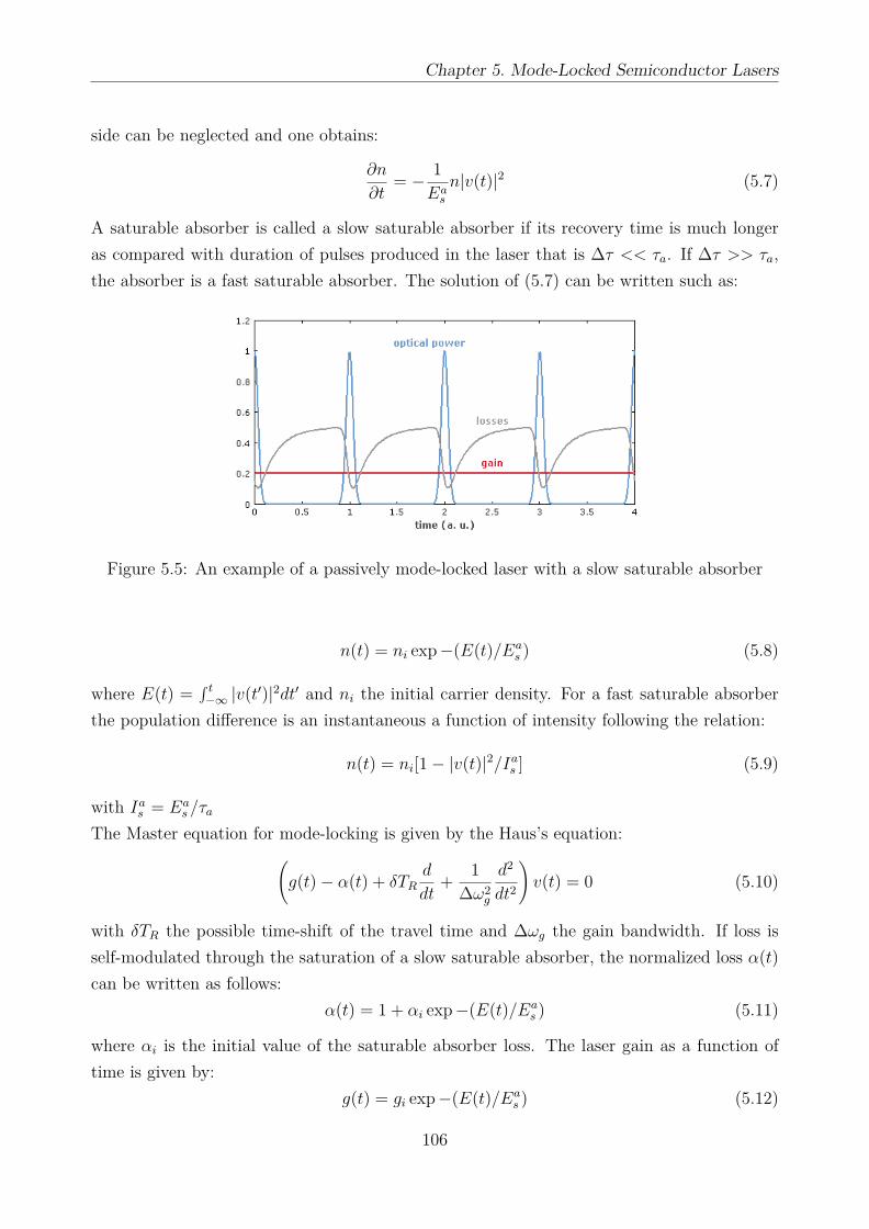
Chapter 5. Mode-Locked Semiconductor Lasers
side can be neglected and one obtains:
∂n
∂t= − 1
Eas
n|v(t)|2 (5.7)
A saturable absorber is called a slow saturable absorber if its recovery time is much longeras compared with duration of pulses produced in the laser that is ∆τ << τa. If ∆τ >> τa,the absorber is a fast saturable absorber. The solution of (5.7) can be written such as:
Figure 5.5: An example of a passively mode-locked laser with a slow saturable absorber
n(t) = ni exp−(E(t)/Eas ) (5.8)
where E(t) =∫ t−∞ |v(t′)|2dt′ and ni the initial carrier density. For a fast saturable absorber
the population difference is an instantaneous a function of intensity following the relation:
n(t) = ni[1− |v(t)|2/Ias ] (5.9)
with Ias = Eas /τa
The Master equation for mode-locking is given by the Haus’s equation:(g(t)− α(t) + δTR
d
dt+ 1
∆ω2g
d2
dt2
)v(t) = 0 (5.10)
with δTR the possible time-shift of the travel time and ∆ωg the gain bandwidth. If loss isself-modulated through the saturation of a slow saturable absorber, the normalized loss α(t)can be written as follows:
α(t) = 1 + αi exp−(E(t)/Eas ) (5.11)
where αi is the initial value of the saturable absorber loss. The laser gain as a function oftime is given by:
g(t) = gi exp−(E(t)/Eas ) (5.12)
106

5.3. Passive-Mode Locking
where gi is the initial gain just before the pulse arrival. By introducing (5.11) and (5.12) into(5.10), one obtains:(
gie−(E(t)/Eas ) − 1− αie−(E(t)/Eas ) + δTR
d
dt+ 1
∆ω2g
d2
dt2
)v(t) = 0 (5.13)
This is a nonlinear integro-differential equation. A simple solution of the equation is obtainedif one expands the exponentials into power series and break them off with second order terms(weak saturation). For Ea
s << Eag , the solution of resulting equation is,
v(t) = v0
cosh t/τp(5.14)
Substituting (5.14) into (5.13) and equating terms of equal powers of tanh(t/τp), one obtainsthree characteristics equations for the determination of the pulsewidth, detuning and pulseenergy. Also, it is important to stress that the conditions
gi
(EpEgs
)2< αi
(EpEas
)2
(5.15)
and,gi < 1 + αi (5.16)
must be met if the pulsewidth is to be real. Inequality (5.15) implies that the saturableabsorber must be more easily bleached as compared to the gain medium. Condition (5.16)means that for stable mode-locking, the initial gain should be less than the initial loss. Thesolution of the characteristic equations shows that the pulsewidth τp varies inversely with thepulse energy Ep.This conclusion is also valid for mode-locking with a fast saturable absorber. Let us considerthis type of mode-locking by following the approach developed by Haus for a ring laser cavityconfiguration as shown in figure 5.6. In this case the pulse envelope denoted A(z, t) is afunction of time and a spatial coordinate z. The mode-locking equation can be written suchas:
∂A
∂t+ 1vg
∂A
∂t= g
(1 + 1
∆ω2g
∂2
∂t2
)A− α0
1 + |A|2Ias
A (5.17)
In order to solve this equation, one can approximate,1
1 + |A|2Ias
≈ 1− |A|2/Ias (5.18)
This approximation and a transformation of the independent variables ξ = z, η = t − z/vgallows to re-write (5.17) into the form:
−∂A∂ξ
+ (g − α0)A+ g1
∆ω2g
∂2A
∂η2 + α0|A|2
IasA = 0 (5.19)
107

Chapter 5. Mode-Locked Semiconductor Lasers
Figure 5.6: Schematic of a ring cavity used for mode-locking
When a steady-state pulse forms
∂
∂ξ= ∂
∂z+ 1vg
∂
∂t= 0 (5.20)
and (5.19) can be reduced to,
(g − α0)A+ g1
∆ω2g
∂2A
∂η2 + α0|A|2
IasA = 0 (5.21)
The finite bandwidth of the gain causes spreading of the pulse in time as described by thetemporal diffusion operator ∂2/∂η2. This diffusion time is balanced by the saturable lossterm proportional to |A|2. Equation (5.21) has a solution which can be written as follows,
A(z, t) = A0
cosh γ(z − vgt)(5.22)
with
vgγ =(α0
2g∆ω2g
|A0|2
Ias
)1/2
(5.23)
andα0 − g = g
∆ω2g
(vgγ)2 (5.24)
Expression (5.23) expresses the pulsewidth , which for the secant hyperbolic pulse is:
FWHM = 2 ln 2(1 +√
2)vgγ
≈ 1.76(
2gIasα0∆ω2
g |A0|2
)1/2
(5.25)
108

5.4. Colliding Pulse Mode-Locking
which shows that more powerful power pulses should be shorter. It also implied that shorterpulses can be obtained with an absorber that can be more easily saturated that is with lowerIas . A secant hyperbolic pulse shape in passively mode-locked lasers with a low saturationlevel (Ep << Ea
s , Egs ) is consistent with experimental results. However, it should be stressed
that for more powerful pulses, the pulse shape may be distorted by gain and loss saturationand the asymmetric pulses may be generated in the laser.
5.4 Colliding Pulse Mode-Locking
The colliding pulse mode-locking technique (CPM) has been shown to be very effective increating optical pulses that are in the femtosecond range. CPM utilizes the forward andbackwards traveling light inside the laser cavity to build up a transient standing wave. Anexample of a monolithic CPM laser is shown in figure 5.7. The ultra-short pulses are achievedby having these forward- and backward-traveling waves collide inside the absorber section andsaturating (bleaching) the section. This collision creates a spike in optical intensity creatingan associated pulse. The collision creates a much stronger saturation of the absorber thanwould be possible with just a single pulse traveling through at one time. The length of theabsorber section can control the ease and quality of mode locking. The absorber introduces
Figure 5.7: Schematic view of a monolithic colliding pulse mode-locked laser (CPM)
a nonlinearity that leads to a change in pulse shape, which causes the pulse to compress. Ifthe colliding pulses traveling into the absorber section are relatively large compared to theabsorber, the resultant pulse will undergo significant compression due to the short length ofthe absorber section. This pulse will not only have significant compression, but it will benear the saturation energy of the gain section. The energy associated with the wide pulse isconserved, but is now confined into a smaller pulse width, which results in a greater intensity.This is a very important aspect to CPM because it allows passively mode- locked laser tooperate at low pulse energy for maximum compression while still providing adequate opticalpower. It is also possible to apply this technique in order to generate higher order harmonicsof the laser’s fundamental frequency.
109

Chapter 5. Mode-Locked Semiconductor Lasers
Double-Interval Mode-Locking Technique
Double-interval mode-locking takes advantage of a semiconductor laser’s ease of reconfig-urability and harmonic mode-locking. The double-interval technique (see also section 5.6)refers to using two saturable absorbers that independently stimulate harmonics of the de-vice in order to achieve the multiplicative value of the two harmonics. The double intervaltechnique is similar to CPM in that it utilizes saturable absorbers to create a pulse. Theunique aspect of the double-interval technique is that by creating two saturable absorbersections within the laser cavity, it is possible to create a condition where the pulses createdcan collide together and affect each other. By using this knowledge, it is possible to placethe absorbers in specific locations in order to create the desired optical pulse. For example,to stimulate the laser’s tenth harmonic a saturable absorber can be placed in the midpointof the laser diode and another at a point corresponding to a fifth of the laser diode. Indi-vidually they would stimulate the second and fifth harmonics, but with the double-intervaltechnique they are stimulated simultaneously and result in the stimulation of the tenth har-monic. A harmonically mode-locked laser produces an optical pulse train at a multiple ofthe fundamental round-trip frequency. This is very advantageous for semiconductor lasersbecause they already have a high fundamental frequency due to their short cavity length.Combined with the double interval technique it is possible to get very high repetition ratesfrom semiconductor laser diodes. Photolithography techniques and mask designs can create asegmented semiconductor laser diode, but as more and more divisions are desired it becomesdifficult to achieve good results. Double interval harmonic mode-locking is beneficial becauseit overcomes the limitations introduced by standard processing. By utilizing this techniqueit is possible to lock to higher order harmonics that would correspond to repetition ratesthat would be very difficult to achieve by just mode-locking alone. As seen in figure 5.8 itis possible to segment the device for the double-interval technique or into divisions that willallow for the simulation of the desired harmonic. In the case for figure 5.8, it is desired tostimulate the 10th harmonic of the device. Traditionally this would require the device to besegmented in order to isolate a section that would correspond to a tenth of the device. Asdiscussed earlier this may be limited to photolithography techniques and as dimensions getsmaller it becomes difficult to wire-bond and probe the device. With the double- intervaltechnique it is possible to maintain larger segments and stimulate the 10th harmonic.
110

5.5. Monolithic Quantum Dot Passively Mode-Locked Lasers
Figure 5.8: Comparison between device segmentation for double-interval mode-locking andtraditional mode-locking for the 10th harmonic of a laser diode
5.5 Monolithic Quantum Dot Passively Mode-LockedLasers
In the early 1990’s there was considerable interest in mode-locked semiconductor lasers andtheir potential use in high-speed optical systems,which require a compact, low jitter sourcethat could produce picosecond pulses. This work culminated in the demonstration by BellLabs of the 350 GHz colliding pulse modulated laser. What ultimately discouraged furtherefforts was the complexity and expense of the electronics for the active and hybrid mode-locking that were necessary to stabilize the pulse train. Passively mode-locked semiconductorlaser sources, which require no synchronization by external drivers circuits were greatly pre-ferred for their simplicity, but were plagued with large timing jitter (>10 ps), because of thesignificant amplified spontaneous emission noise generated by the quantum well (QW) activeregion. This large timing jitter limited the usefulness of short pulse devices. The QW devicesalso had limited power output in the pulses due to mode competition above threshold andnon- linear gain effects.Recently, these issues with power and jitter have been significantly improved upon usingquantum dot active regions. The typical device configuration of these next-generation QDMLLs is shown in figure 5.9. Two of the advantages of QDs that are exploited are the lowersaturation intensity that is needed to bleach the absorber section and the ability to run thegain section under strong inversion for high peak pulsed powers. These two features thatmake QD MLLs easier to lock and operate can be summarized in an important figure ofmerit for mode-locked lasers, the ratio of the saturation energy of the gain section to the
111

Chapter 5. Mode-Locked Semiconductor Lasers
saturation energy of the absorber:
Esat,gEsat,a
=hνAmΓ dgdN
NthνAm= 1
ΓNtdgdN
(5.26)
where Am is the cross-sectional area of the optical mode, Γdg/dN is the differential modal gain(or optical cross-section), and Nt is the optical transparency density. These three parametersall have units of cm−2. The transparency density is directly controlled by the dot density,the lower limit of which is essentially limited only by the internal loss of the optical cavity.The differential gain in a quantum dot ensemble can also be made very small because thegain saturation of quantum dots with volumetric carrier density, N (cm−3), is so strong.This effect has been used to great advantage in designing reconfigurable quantum dot mode-locked lasers. QW gain regions also have 2-3 times larger transparency densities which isundesirable as seen in the figure of merit equation above. Mode-locking is not a guarantee
Figure 5.9: Schematic diagram of a 2-section monolithic MLL with QD gain and absorberregions. The facet at the absorber end of the device is HR coated to produce the quasi-colliding pulse mode-locking effect and narrow the pulse width
that there is no jitter in the output pulses. Even when the laser is mode-locked, there canbe phase instabilities between the frequencies that make up the pulse. Indeed, to generatestable optical combs for metrology, great lengths must be placed on both carrier envelopphase stabilization and frequency locking of the comb. Such systems would have very lowjitter and noise. Unfortunately, they are large, fragile, and complex. The compact size,low power consumption, direct electrical pumping of semiconductor MLLs make them well-suited for optical clocking in applications such as analog-to-digital conversion as well ashigh bit-rate optical time division multiplexing, electro-optic sampling, and impulse response
112

5.5. Monolithic Quantum Dot Passively Mode-Locked Lasers
measurement of optical components. For these applications, low timing jitter of the ultra-short optical pulses is required since the fluctuation of the pulse arrival time degrades bit-errorrate and time resolution. Among the different MLL configurations, the monolithic 2-sectionpassively mode-locked semiconductor laser is the most desirable option for low-cost high-volume production due to device compactness and system simplicity. However, previous QWmonolithic, passive MLLs have suffered from much larger timing jitter compared to active orhybrid MLLs. The timing jitter in passive MLLs arises from the fluctuations in carrier density,photon density, and index of refraction caused by the amplified spontaneous emission (ASE).Due to the discrete energy levels and low transparency current in a QD gain medium, theportion of carriers involved in the non-stimulated emission is significantly reduced. Therefore,low ASE is expected in QD devices, suggesting that a lower timing jitter can be achievedwith QD passive MLLs compared to QW passive MLLs. Detailed measurements of the jitteras a function of injected current in the gain section and constant voltage on the saturableabsorber showed that the jitter initially decreases with current, reaches a minimum, and thenincreases again at higher bias. This phenomenon is shown in figure 5.10 for various absorbervoltages. That is, near threshold, spontaneous emission and stimulated emission compete,causing incomplete mode-locking, which, in turn makes the jitter higher. As the output
Figure 5.10: The measured jitter of a QD MLL as a function of gain section current forvarious absorber voltages. 500 fs jitter is routinely achieved in this device
power increases (with increasing bias current) in these quantum dot lasers, the linewidthenhancement factor begins to increase causing an increase in the coupling between the phaseand the amplitude. Thus, intensity noise couples more strongly into phase noise, increasingthe jitter. The same trend occurs in the pulse width of the device meaning that in QD
113

Chapter 5. Mode-Locked Semiconductor Lasers
MLLs the jitter behavior seems to be closely correlated with the pulse width one. Furtherimprovement in the jitter can be realized using optical injection. It is anticipated that opticalinjection will improve the jitter by roughly a factor of 5.
5.6 Colliding Pulse Technique for Higher Order Har-monic Generation
The double-interval technique utilizes colliding pulses to generate higher order harmonics ofa semiconductor laser diode. Using the colliding pulse technique, higher order harmonics ofthe repetition rate can be excited. Analogous to the method used by a violinist to create highorder harmonic sounds, the colliding pulse technique can create higher order harmonics of alaser’s fundamental frequency. The difference is with the mode-locked laser, anti-nodes arecreated rather than nodes. When a violinist places his finger upon a string he creates a nodethat changes the tune of the violin as it is strummed. The strumming of the violin withoutthe violinist placing a finger upon the fingerboard creates the first harmonic also known asthe fundamental harmonic. If the location of the node were in the center of the fingerboard,this would result in the creation of the second harmonic. Placing the finger at a location at athird, fourth, or fifth of the fingerboard will result with the third, fourth, and fifth harmonics,respectively. For instance, figure 5.11 shows the locations of nodes and the correspondingharmonics. By stimulating multiple nodes simultaneously, it is possible to create higher orderharmonics that are equivalent to the product of the nodes’ harmonics. Since it is possibleto create the second and fifth harmonics separately, applying both nodes concurrently willcreate the tenth harmonic. This technique can be extended to a device to create the higherorder harmonics of the laser’s fundamental repetition rate. When applied to a mode-lockedlaser technique, applying a reverse bias to the corresponding location creates an absorbersection. If this absorber is saturable, not strong enough to absorb all of the excess carrierspresent, then it behaves as an anti-node. This saturable absorber is an anti-node because itcreates a location where a maximum can occur rather than a fixed minimum as with a node.It is these anti-nodes that are needed to provide the generation of the higher order harmonics.Also, obtaining high order harmonics would be difficult to achieve by simply creating a singleanti-node. This would require placing the anti-node at a division of the laser that mightbe impractical to achieve. Thus multiple anti-nodes can be used to generate the desiredharmonic using the double-interval technique. Figures 5.12 and 5.13 show an example of alaser diode with anti-nodes corresponding to the second and fifth harmonics which are usedto create the tenth harmonic. This allows for the generation of harmonics that would not bepossible to create with just one anti-node. With this device in particular, when the saturable
114

5.6. Colliding Pulse Technique for Higher Order Harmonic Generation
Figure 5.11: Location of nodes and corresponding harmonic generated
Figure 5.12: Laser anti-nodes for creation of tenth harmonic
Figure 5.13: Segmented device for higher harmonic generation
115

Chapter 5. Mode-Locked Semiconductor Lasers
absorber was placed close to the sections corresponding to the fundamental repetition rate,the fundamental repetition rate was excited. So to stimulate the tenth harmonic with just onesaturable absorber at the location corresponding to 25 was not possible because it stimulatedthe fundamental harmonic. Figure 5.14 shows the Radio Frequency (RF) spectrum for thefundamental, 2nd, 3rd, 5th, and 6th harmonics of the QD mode-locked laser depicted in figure5.13. Since it is desired to have the pulses collide inside the saturable absorber, the forwardand backwards traveling waves must be of enough combined intensity in order to saturatethe absorber. As stated earlier, in order to generate optical pulses for a passive mode-lockedlaser the loss must saturate faster than the gain. This introduces the stability condition s ofa passively mode-locked laser described by (5.26). The stability condition gauges the qualityof the laser’s mode-locking and is used as a guideline for getting into the locking regime.
Figure 5.14: 50 GHz span of the mode-locked laser’s fundamental harmonic (6.0 GHz), 2ndharmonic (12.0 GHz), 3rd harmonic (18.0 GHz), 5th harmonic (30.0 GHz), and 6th harmonic(36.0 GHz)
116

Chapter 6
Injection-Locking of SemiconductorDiode Lasers
6.1 Introduction
Optical-injection of semiconductor lasers involves two optical sources referred to as the masterand slave lasers as seen in figure 6.1. The master laser, typically a high- power single-modenarrow-linewidth tunable laser, is injected into the slave laser, thereby affecting the operationand inherent free-running characteristic parameters of the slave laser. An isolator is placedbetween master and slave lasers to eliminate reflected light coupling back to the master laser.Under stable injection-locking of semiconductor lasers, which occurs when the strength of theinjected master laser light and frequency difference between the master and slave fall withina certain range, the slave’s lasing wavelength is pulled/locked to the injected master laser’swavelength. Stable injection- locking provides several improvements to directly-modulatedlasers. These improvements include increasing the modulation bandwidth, suppressing non-linear distortion, and reducing relative intensity noise, mode hopping, and chirp. A ba-
Figure 6.1: Principle of an Injection-Locked Semiconductor Laser Diode
sic example of the spectral improvements under stable injection-locking for a multi- modeFabry-Perot quantum-dash slave laser was already shown in figure 1.14. An example of
117

Chapter 6. Injection-Locking of Semiconductor Diode Lasers
the modulation bandwidth enhancement for the injection-locked Fabry-Perot quantum-dashsemiconductor laser is shown in figure 6.2. The characteristics of the modulation responsecurves in figure 6.2 are observed to vary as a function of the detuning frequency betweenthe master and slave lasers for a fixed injection strength. Besides the stable injection-locking
Figure 6.2: Modulation response of the injection-locked quantum-dash laser for varied fre-quency detuning (∆f) conditions.
regime, the optically-injected system demonstrates a dynamic behavior whereby the opticalspectra are characterized by the appearance of relaxation oscillation sidebands and coherencecollapse. The optical power spectra associated with the dynamic states exhibited by a diodelaser under optical-injection are referred to as period-one, period-doubling, four-wave mixing,and coherence-collapse, and are illustrated in figure 6.3. The optical spectra shown in figure6.3 are unique in nature due to the high resolution of the spectrometer used in data collec-tion (maximum resolution = 1 MHz), which allowed extreme detail of the optically-injectedquantum-dash laser’s behavior to be observed. In figure 6.4 and throughout this work, thedetuning frequency is defined as:
∆f = fmaster − fslave (6.1)
An unlocked system, where either the injected signal strength is weak and/or the frequencydifference is too large resulting in the master laser field having no impact on the slave laser, isshown in figure 6.3(a). The period-one state, illustrated in figure 6.3(b), is characterized by
118

6.2. Applications of Optically-Injected Lasers
the presence of undamped relaxation oscillation sidebands. Figure 6.3(c) shows the period-doubling state which is similar to the period-one state, but with additional relaxation oscil-lation side-bands associated with a second periodic-oscillator at roughly half the slave laser’scharacteristic relaxation oscillation frequency. Stable locking is shown in figure 6.3(d) andis characterized by single mode operation with a significant degree of side mode suppression(defined here as > 30- dB), where the single locked-mode has a narrow linewidth, reducedchirp and noise compared to the slave laser’s free running characteristics. The small sidemodes (side mode suppression > 40 dB) in figure 6.3(d) are attributed to residual feedbackin the experimental setup. The coherence-collapse state pictured in figure 6.3(e) is character-ized by a large broadening of the coupled system’s linewidth. Four-wave-mixing is shown infigure 6.3(f) and is a described as a pseudo-unlocked state where two additional frequenciesare generated due to optical non-linearities in the device. Under four-wave mixing, the slavelaser’s operating frequency is unaffected by the injected power. For a fixed injected masterpower, the coupled system will progress from the period-one state to four-wave- mixing forincreased detuning frequencies and a clear boundary is typically difficult to quantitativelydetermine. The microwave modulation response under period-one, period- doubling, and co-herence collapse are normally considered undesirable for use in high-speed coherent opticalcommunication systems where the slave laser is directly- modulated. With the optical powerspectral descriptions describing the operational states (stable-locking, period-one, period-doubling, coherence collapse, four-wave-mixing), stability maps characterizing the dynamicstate as a function of the maximum injection strength and detuning frequency can be con-structed for a given slave laser. An example is illustrated in figure 6.4 for a quantum-dashFabry-Perot slave laser. The relatively stable operation under zero frequency-detuning condi-tions and the large period-one oscillation state parameter space open the quantum-dash laserto possible applications as a tunable photonic oscillator or directly-modulated slave laser ina coherent optical communication system.
6.2 Applications of Optically-Injected Lasers
Communication applications of optically-injected semiconductor lasers have predominantlyfocused on the stable locking state achieved under strong injection where desirable highfrequency modulation characteristics have been exhibited. Recently, however, the complexnonlinear dynamical states resulting from the optical- injection of semiconductor lasers havegenerated increased interest for many novel applications. Potential applications based ontheir rich nonlinear dynamics include: chaotic communications, chaotic lidar, chaotic radar,photonic microwave generation, dual-frequency precision radar/lidar, all-optical AM-to-FMconversion, and single-sideband radio-over-fiber transmission. In this section, the applications
119
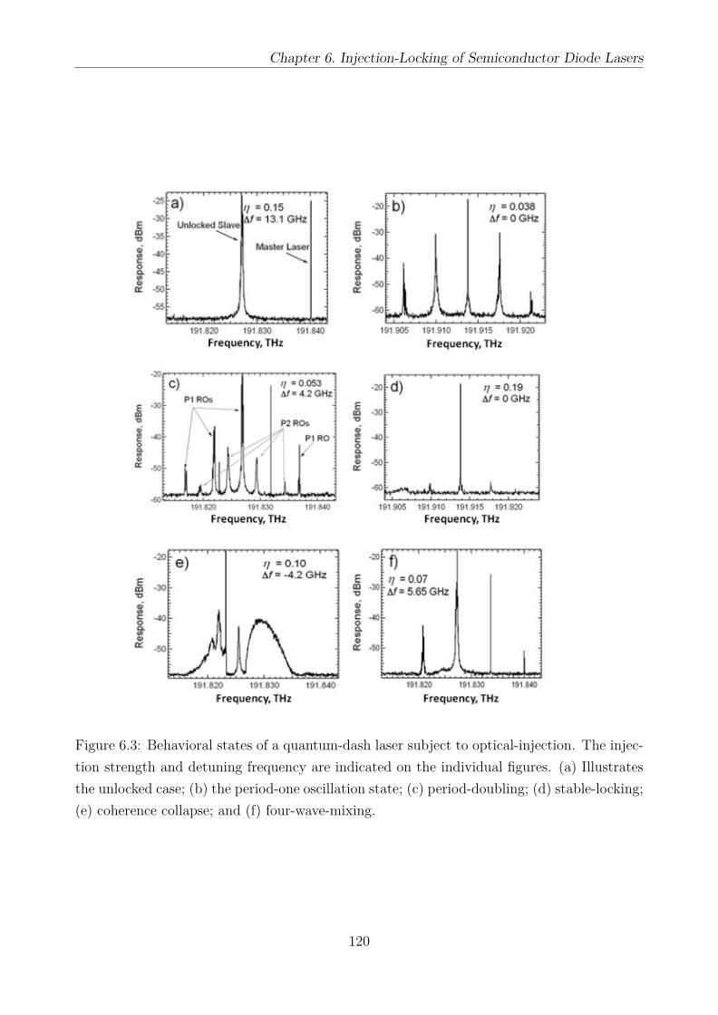
Chapter 6. Injection-Locking of Semiconductor Diode Lasers
Figure 6.3: Behavioral states of a quantum-dash laser subject to optical-injection. The injec-tion strength and detuning frequency are indicated on the individual figures. (a) Illustratesthe unlocked case; (b) the period-one oscillation state; (c) period-doubling; (d) stable-locking;(e) coherence collapse; and (f) four-wave-mixing.
120

6.2. Applications of Optically-Injected Lasers
of the period-one operational state are discussed.The period-one state is described as the condition where the slave laser is locked to the
injected field and the coupled system oscillates at the injected frequency (finj) with side-bands at frequencies of finj−fr, where fr is the resonance frequency of the optically-injectedlaser as illustrated in figure 6.5. The resultant electric field of the optically-injected slavelaser oscillates without being damped towards a steady-state value as in a free-running orstable-locked semiconductor laser. The period-one resonance frequency is tunable based onthe injection strength and/or detuning frequency between the master and slave laser, gener-ating a microwave modulation on the laser output in an all-optical manner. Compared with
Figure 6.4: Stability map for an optically-injected quantum-dash slave laser at a bias currentof 65 mA showing only stable and period-one operation at zero-detuning and a large period-one parameter space as the injection strength and/or detuning frequency are varied. Theblue diamonds at negative detuning indicate chaotic (coherence collapse) operation. Thetrendlines have been added as a visual aid only.
direct modulation, external modulation, mode-locking, self pulsation, and optical phase-lockloops, the period-one approach presents several advantages in microwave generation. Theprimary advantage identified is that the all-optical approach of optical-injection avoids thelimitations of microwave electronics and electrical parasitics. In this regard, the system iscontrolled using the DC injection current of the master laser to modulate its output powerresulting in a tunable resonance frequency varying from the free-running laser’s natural re-laxation oscillation frequency to up to six times this value. Generation of period-one mi-crowave frequencies up to 60 GHz have even already been reported, making the period-one
121

Chapter 6. Injection-Locking of Semiconductor Diode Lasers
optical-injection system an ideal radio-over-fiber source. Radio over Fiber (RoF) refers to a
Figure 6.5: Optical power spectra of an optically-injected quantum-dash laser under a biasof 65 mA in the period-one oscillation state. The injected field ratio and detuning frequencyare indicated on each plot. fr is the measured resonance frequency. ∆f is the detuningfrequency.
technology whereby light is modulated by a radio signal and transmitted over an optical fiberlink to facilitate wireless access. Although radio transmission over fiber is used for multiplepurposes, such as in cable television (CATV) networks and in satellite base stations, theterm RoF is usually applied when this is done for wireless access. In RoF systems, wirelesssignals are transported in optical form between a central station and a set of base stationsbefore being radiated through the air. Each base station is adapted to communicate over aradio link with at least one user’s mobile station located within the radio range of said basestation. RoF transmission systems are usually classified into two main categories (RF-over-Fiber ; IF-over-Fiber) depending on the frequency range of the radio signal to be transported.
a) In RF-over-Fiber architecture, a data-carrying RF (Radio Frequency) signal with ahigh frequency (usually greater than 10 GHz) is imposed on a lightwave signal before beingtransported over the optical link. Therefore, wireless signals are optically distributed to basestations directly at high frequencies and converted to from optical to electrical domain at thebase stations before being amplified and radiated by an antenna. As a result, no frequencyup/down conversion is required at the various base station, thereby resulting in simple andrather cost-effective implementation is enabled at the base stations.
b) In IF-over-Fiber architecture, an IF (Intermediate Frequency) radio signal with a lower
122

6.2. Applications of Optically-Injected Lasers
frequency (less than 10 GHz) is used for modulating light before being transported over theoptical link. Therefore, wireless signals are transported at intermediate frequency over theoptical.
Advantages of Radio-over-Fiber- Low Attenuation: It is a well known fact that signals transmitted on optical fiber atten-
uate much less that other medium, especially when compared to wireless medium. By usingoptical fiber, the signal will travel further reducing the need of repeaters.
- Low Complexity: RoF makes use of the concept of a Remote Station (RS). This stationonly consists an optical-to-electrical (O/E) (and an optional frequency up or down converter),amplifiers, and the antenna. This means that the resource management and signal genera-tion circuitry of the Base Station can be moved to a centralized location and shared betweenseveral remote stations, thus simplifying the architecture.
- Lower Cost: Simpler structure of remote base station means lower cost of infrastructure,lower power consumption by devices and simpler maintenance all contributed to lowering theoverall installation and maintenance cost. Further reduction can also be made by use of lowcost Graded Index Polymer Optical Fiber (GIPOF).
- Future Proof: Fiber Optics are designed to handle gigabits speeds which means theywill be able to handle speeds offered by future generations of networks for years to come.RoF technology is also protocol and bit-rate transparent, hence, can be employed to use anycurrent and future technologies.
Applications of Radio-over-fiber
- Access to dead zones: An important application of RoF is its use to provide wirelesscoverage in the area where wireless backhaul link is not possible. These zones can be areasinside a structure such as a tunnel, areas behind buildings, Mountainous places or secludedareas such a jungle.
- FTTA (Fiber to the Antenna): By using an optical connection directly to the antenna,the equipment vendor can gain several advantages like low line losses, immunity to lighteningstrikes/electric discharges and reduced complexity of base station by attaching light weightOptical-to-Electrical (O/E) converter directly to antenna.
123

Chapter 6. Injection-Locking of Semiconductor Diode Lasers
The frequency tunability of the period-one resonance frequency based on the strengthof the injected signal opens the possibility of all-optical AM-to-FM conversion, enabling theintegration of the optical-injection architecture into radio-over-fiber systems. In the AM-to-FM conversion application, the input amplitude modulated signal is used to drive the masterlaser injecting the slave laser under a condition that results in the period-one oscillationstate; the amplitude modulated signal injecting the slave laser will then be converted to afrequency modulated microwave signal. The optical-injection based AM-to-FM frequencymodulation conversion increases bandwidth capabilities, and reduces signal distortion, elec-tronic noise, and power consumption. A depiction of the radio-over-fiber architecture usingoptical-injection to perform the AM-to-FM conversion is given in figure 6.6.
Figure 6.6: Generic depiction of the radio-over-fiber architecture. The AM-to-FM conversionis performed at the central office and the FM modulated optical signal is transmitted to thebase stations simplifying base station processing requirements.
6.3 Theoretical Description
In order to understand the limiting factors in an injection-locked system it is important toinvestigate the governing theory that can be obtained by modeling the characteristic param-eters using a set of coupled rate equations. Mathematical translation of the injection-lockingsystem operating in the stable locking regime based on three fundamental rate equations.The Lang and Kobayashi model was initially proven to be valid only for weak injection cases;however, with some minor changes it has been shown to be useful in predicting the operat-ing properties of the system regardless of the magnitude of injection strength. This section
124

6.3. Theoretical Description
capitalizes on improvements to the rate equations governing the dynamic properties of aninjection-locked system in order to investigate the modulation properties of such a systemunder strong injection.
6.3.1 Rate Equations
The differential equations describing the dynamics of an injection-locked system have beendeveloped by introducing terms describing the impact of optical injection to the conventionalrate equations governing the free-running characteristics of the slave laser. The additionalterms include a coupling value, kc, the magnitude of the injected master field, Ainj, and thedetuning frequency between master and slave, ∆ω. The model assumes the slave laser is beingdirectly modulated such that the small signal approximation can be applied. Additionally, itis assumed that the laser has been exposed to a relatively strong external optical injection,such that the impact of the noise and the spontaneous emission rate coupled to the lasingmode are negligible. The free-running Fabry-Perot slave laser has cleaved facets and is biasedwell above threshold. As in the free running case, the amplitude and phase equations arisefrom the fundamental complex field rate equation. The variation of the slave field magnitude,phase offset between the master and slave fields and carrier density with time can be writtenas :
dA
dt=(g
2∆N)A+ (kc cos(φ))Ainj (6.2)
dφ
dt= α
(g
2∆N)A−∆ω − (kc sin(φ)) Ainj
A(6.3)
dA
dt= Jbias − γNN − (γP + g∆N)A2 (6.4)
where A is the internal slave’s amplitude of the electric field, g is the differential gain, N isthe carrier density and ∆N = N − Nth is the shift in carrier density from the threshold. φis the phase offset between master and slave laser, which is defined as φslave − φmaster, theamplitude of the electric field square, A2, is proportional to photon density P and Jbias, γN ,γP correspond to the applied bias current density, inverse differential carrier lifetime andphoton decay rates, respectively. It is important to note that the phase variation in timedepends on detuning through ∆ω = ωslave − ωmaster. The linewidth enhancement factor, α,injection strength which is proportional to Ainj/A, phase offset φ, and detuning term ∆ωinjare the key and defining injection parameters that have a significant impact on the coupledoscillator system.
125
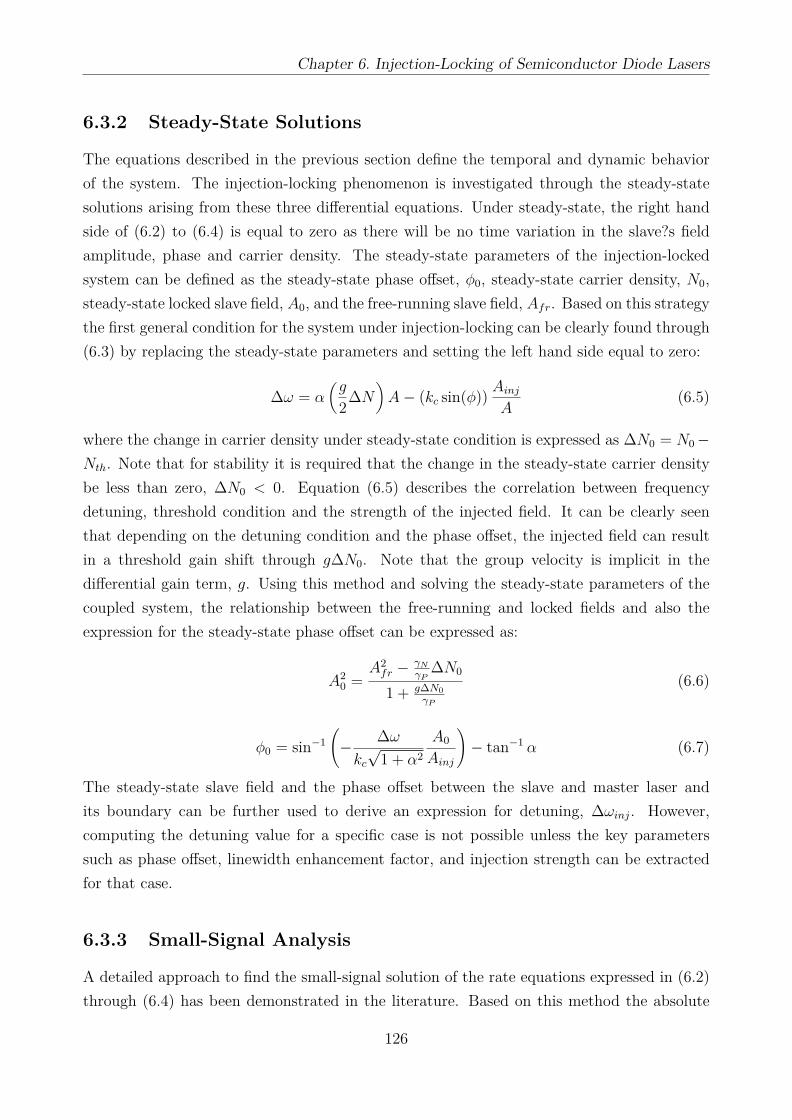
Chapter 6. Injection-Locking of Semiconductor Diode Lasers
6.3.2 Steady-State Solutions
The equations described in the previous section define the temporal and dynamic behaviorof the system. The injection-locking phenomenon is investigated through the steady-statesolutions arising from these three differential equations. Under steady-state, the right handside of (6.2) to (6.4) is equal to zero as there will be no time variation in the slave?s fieldamplitude, phase and carrier density. The steady-state parameters of the injection-lockedsystem can be defined as the steady-state phase offset, φ0, steady-state carrier density, N0,steady-state locked slave field, A0, and the free-running slave field, Afr. Based on this strategythe first general condition for the system under injection-locking can be clearly found through(6.3) by replacing the steady-state parameters and setting the left hand side equal to zero:
∆ω = α(g
2∆N)A− (kc sin(φ)) Ainj
A(6.5)
where the change in carrier density under steady-state condition is expressed as ∆N0 = N0−Nth. Note that for stability it is required that the change in the steady-state carrier densitybe less than zero, ∆N0 < 0. Equation (6.5) describes the correlation between frequencydetuning, threshold condition and the strength of the injected field. It can be clearly seenthat depending on the detuning condition and the phase offset, the injected field can resultin a threshold gain shift through g∆N0. Note that the group velocity is implicit in thedifferential gain term, g. Using this method and solving the steady-state parameters of thecoupled system, the relationship between the free-running and locked fields and also theexpression for the steady-state phase offset can be expressed as:
A20 =
A2fr − γN
γP∆N0
1 + g∆N0γP
(6.6)
φ0 = sin−1(− ∆ωkc√
1 + α2
A0
Ainj
)− tan−1 α (6.7)
The steady-state slave field and the phase offset between the slave and master laser andits boundary can be further used to derive an expression for detuning, ∆ωinj. However,computing the detuning value for a specific case is not possible unless the key parameterssuch as phase offset, linewidth enhancement factor, and injection strength can be extractedfor that case.
6.3.3 Small-Signal Analysis
A detailed approach to find the small-signal solution of the rate equations expressed in (6.2)through (6.4) has been demonstrated in the literature. Based on this method the absolute
126

6.3. Theoretical Description
modulation frequency response function can be expressed as:
|H(ω)|2 =∣∣∣∣∣∆A∆J
∣∣∣∣∣2
= |M |2(ω2 + Z2)(C − Aω2)2 + (Bω − ω3)2 (6.8)
where the parametric terms A, B, C, Z and M can be defined and simplified as:
A = 2η cosφ0 + γN + gA20 (6.9)
B = η2 + 2η cosφ0(gA20 + γN) + gA2
0(γP − 2η cosφ0) (6.10)
C = η2(γN + gA20)− gA2
0(γP − 2η cosφ0)Z (6.11)
Z = η(α sinφ0 − cosφ0) (6.12)
M = g
2A0 (6.13)
The injection strength is proportional to the coupling term and the field ratio as:
η = kcAinjA0
= η0
RFE
(6.14)
where η0 is the maximum injection ratio and RFE = A0/Afr is the slave field enhancementfactor due to injection. η0 incorporates the external master to slave power ratio, the couplingefficiency between the slave and master laser, and efficiency of injected field entering theslave laser cavity due to facet reflectivity. At this point, the enhancement of the slave fieldis introduced as an additional term denoted as the field enhancement factor, RFE, whichtakes into account the deviation of the slave steady-state field magnitude compared to itsfree-running value at high injection ratios and specific frequency detuning.
6.3.4 Modulation Response Model
The modulation response model expressed in (6.8) can be used to simulate the modulationcharacteristics of an injection-locking system in microwave domain. However, since there areas many as 8 fitting parameters involved in this model, such a large number of potentially un-constrained parameters allows for many possible solutions that would reduce the confidencein extracted results. Thereby, one of the goals is to reduce the number of fitting parame-ters through known free-running slave terms along with additional constraints on remaininginjection-locking fitting terms. Doing so, the parametric terms A, B, C, and Z definedin (6.8) can be translated in terms of known free-running and injection-locked parameters.This reduces the fitting parameters while the remaining terms are expressed with respect
127

Chapter 6. Injection-Locking of Semiconductor Diode Lasers
to the injection-locking operating parameters of the system which then will be projected inthe targeted relative modulation response function. Since the M2 term defined in (6.13) isindependent of frequency, it can be cancelled in the relative modulation response form. TheA term in (6.8), is effectively a damping rate of the coupled oscillator as follows:
A = γslave + γth (6.15)
The slave damping rate, γslave, is related to the free running damping rate and scales withthe field enhancement factor as:
γslave = gA20 + γN = (γfr − γ(N)R2
FE + γN (6.16)
where γfr = gA2fr + γN is the free-running slave damping rate and γN is assumed to be
independent of optical injection. The explicit relationship between the locked and free-running damping rates is a key feature of the current model and allows us to implicitlyinclude non-linear gain effects as explained below. γth is the threshold gain shift and appearsas a damping component resulting from moving the slave from its free-running condition. Itis also related to the phase offset and injection strength such that:
γth = 2η cos(φ0) = 2 η0
RFE
cos(φ0) = −g∆N0 (6.17)
Again it is necessary to note that the group velocity is implicit in the differential gain term,g, everywhere in this derivation. Using (6.16) to substitute for the slave damping rate in(6.15) and re-writing the expression for A, we have:
A = (γfr − γN)R2FE + γN + γth (6.18)
The second and most important term located in the denominator of the response function isB, which corresponds to the overall resonance frequency of the system. Substituting for thethreshold gain shift, γth, in the B term defined in (6.10) and rearranging yields:
B = η2 + γth(gA2
0 + γN)
+ gA20 (γP − γth) (6.19)
The second term in (6.19), which is related to the steady-state slave locked field and carrierlifetime as (gA2
0 + γN), effectively appears as a damping rate which can be directly linked tothe slave damping rate, γslave. Using the definition in (6.16) this term can be replaced asfollowing:
B = η2 + γthγslave + gA20 (γP − γth) (6.20)
By multiplying both sides of the steady state solution of the locked field found in (6.6) bythe differential gain, g, and rearranging γP on the right hand side, yields:
gA20 =
gA2frγP − γNg∆N0
γP + g∆N0(6.21)
128
6.3. Theoretical Description
The first term in the numerator, gA2frγP , corresponds to the free-running relaxation fre-
quency squared,ω2r . Substituting the threshold gain shift defined in (6.17) allows (6.21) to
be rewritten as:gA2
0 =ω2fr + γthγN
γP − γth(6.22)
Substituting (6.14), (6.16) and (6.22) into (6.20) and rearranging will give the followingexpression for the B term:
B =(ω2r + γNγth
)+(η0
RFE
)2+ γth
[(γfr − γN)R2
FE + γN]
(6.23)
For the case of zero injection, η is zero and (6.23) is equal to the relaxation frequency squaredof the slave laser, B = ω2
r , which simply represents the slave’s free-running operating con-dition. Similarly, rearranging (6.14), (6.16), (6.17) and (6.22), C is simplified and expressedas:
C =(η0
RFE
)2[(γfr − γN) R2
FE + γN ]−(ω2r + γNγth
)Z (6.24)
The Z term corresponds to the correlation between the detuning phase offset and linewidthenhancement factor as defined in (6.12).
Z = η0
RFE
(α sin(φ0)− cos(φ0)) (6.25)
By manipulating (6.8) and applying the parametric terms expressed in (6.18) and (6.23)-(6.25), the relative modulation response function of a stably-locked system can be expressedas:
|HR|2 = |H(ω)|2|H(0)|2 =
(CZ
)2(ω2 + Z2)
(C − Aω2)2 + (Bω − ω3)21
1 +(ωγc
)2 (6.26)
It is important to note that the response function expressed in (21) has a cubic frequencydependence. Also, depending on the detuning condition, either the B-containing or C/A-containing terms in the denominator may have a dominant impact on the overall resonancefrequency. The second term in the denominator accounts for the parasitic RC and carriertransport effects where γc is considered as a free-running characteristic constant that can beextracted along with other free-running parameters.
6.3.5 Identifying the Known Free-Running Operating Parameters
By taking into the account all the terms in (6.26) one finds that eight fitting parametersincluding ωr, γfr, γN , γth, η0, RFE, Z and γc are needed for the simulation. All of theterms are expressed as angular frequencies except RFE, and, compared to previous research,represent a different experimental approach that allows an easy comparison of their relativemagnitudes. Since the model is comprised of multiple fitting parameters, there will be many
129

Chapter 6. Injection-Locking of Semiconductor Diode Lasers
solutions available that can fit the experimental data. Most of these possible solutions canbe eliminated by introducing proper restrictions to the operating parameters during least-squares-fitting, such that they can vary only in an acceptable physical range. However,restrictions are not enough to reach a reasonable level of accuracy of the model unless itis combined with a reduction of the freely varying fitting parameters. Fortunately, some ofthese parameters can be extracted from the intrinsic free-running parameters which can bedetermined from the slave laser operating characteristics. The operating parameters of anuncoupled system (free-running slave) can be extracted from the standard and conventionalmodulation response model:
|HR|2 = ω4r
(ω2r − ω2)2 + γ2
frω2
11 +
(ωγc
)2 (6.27)
This expression is used to fit the free-running modulation response and extract three of thefitting parameters: the free-running relaxation oscillation frequency, ωr, the free-runningdamping rate, γfr, and the parasitic roll-off induced by γc. These parameters are intrinsiccharacteristics of the slave laser and remain unchanged when the system is injection-locked.The other fitting parameter found in the free-running characteristics is the inverse differentialcarrier lifetime, γN . This term can be directly extracted by plotting the known free-runningdamping rates as a function of the corresponding relaxation frequencies through the con-ventional expression γfr = Kf 2
r + γN . Knowing the value of γN is beneficial since it mayhave a significant impact on the high frequency behavior of the system under modulation.Consequently, the number of fitting parameters can be reduced from 8 to 4 by keeping thefree-running terms constant during the simulation. Further constraints on the remainingfitting parameters have to be found by considering the theoretical limits of semiconductorphysics.
6.4 Experimental Data and Curve-Fitting Results
6.4.1 Experimental Setup and Data
Fig. 6.7 shows a schematic view of the injection-locking setup used in the experiment. Theslave laser was a multi-mode QDash FP grown on an n+-InP substrate. The laser under studyhas a 4-µm wide ridge waveguide and 500-µm cleaved cavity length. The nominal emissionwavelength of this FP device is around 1560 nm and the threshold current was measured tobe 45 mA at room temperature. The output power of the slave laser was carefully coupledinto a single-mode polarization maintaining (PM) lensed fiber using a piezo-electric stagecontroller with submicron accuracy. The coupling efficiency of the slave laser into the PMlensed fiber was >40%. The PM lensed fiber was connected port 1 of a 3-port PM circulator.
130

6.4. Experimental Data and Curve-Fitting Results
The master laser used in this experiment was a tunable external cavity laser (New Focus6200) with a single-mode PM fiber pigtail connected to the second arm of the circulator, port2. A high resolution (0.01 nm) optical spectrum analyzer (Ando AQ6317B) was connectedto port 3 of the circulator to measure the detuning between the master and slave lasers, aswell as determine stably locked conditions Port 3 of the circulator was connected to a high-
Figure 6.7: Schematic view of the injection-locking QDash experimental setup
speed detector through which the relative modulation response S21 was also measured usingan HP 8722D network analyzer. The 5/95 beam splitter at port 3 of the circulator allowedus to measure the modulation response of the injection locked laser while simultaneouslymonitoring the detuning. This ensured that the desired detuning was stable throughout theexperiment. The modulation responses for various frequency detuning scenarios are providedin Fig. 6.8. The injected power provided by the master laser at the slave arm (port 1 of thecirculator) and the total slave power at both facets, was measured to be 3.5 dBm and 4.7dBm, respectively. The side mode suppression ratio (SMSR) for stable locking was taken tobe 30 dB; using this criterion, stable locking was observed for detuning frequencies from 13.5GHz to -17.1 GHz. At the zero frequency detuning condition, a 3-dB modulation bandwidthof 11.7 GHz was observed, which corresponds to a three-fold improvement relative to the free-running case. At the positive frequency detuning edge, the measured modulation responseexhibits a large sag as well as a high resonance peak. Due to significant damping, only a slightimprovement in the modulation bandwidth is observed for the negative frequency cases.
6.4.2 Model Based Analysis
With the validity of the modulation response model verified based on experimental data, itcan be used to predict injection-locking behaviors for any FP slave laser once its free running
131

Chapter 6. Injection-Locking of Semiconductor Diode Lasers
Figure 6.8: Modulation responses of the free-running and the injection-locked laser underzero and extreme frequency detuning conditions
parameters are known. By knowing the operating parameters of the system it is then possibleto predict the optimum operating limits of the device such as particular detuning frequenciesand the maximum possible bandwidth. One key parameter having a prominent effect on themodulation response is the linewidth enhancement factor. The undesirable sag observed in the
Figure 6.9: Simulation of the modulation response function for various values of the linewidthenhancement factor
modulation response for the extreme positive frequency detuning, as shown experimentally
132

6.4. Experimental Data and Curve-Fitting Results
in Fig. 6.8, can be removed by increasing the linewidth enhancement factor and keepingthe same injection ratio. In Fig. 6.9 the change in the modulation response under extremepositive frequency detuning due to a change in the linewidth enhancement factor is illustratedtheoretically. At the positive frequency detuning edge, the phase offset is roughly π/2 causingthe threshold gain shift to approach zero, γth → 0, and the field enhancement becomes unity,RFE=1. The injection strength and the free-running fitting parameters are kept constant forall three cases.
As shown in Fig. 6.10, the linewidth enhancement factor varies significantly in this device(1.0 to 11) with the bias current. As a consequence of that, the sag in the modulation re-sponse should be removable assuming a high enough injection power is available to maintain aconstant injection ratio. The significance of this observation is that because the highest relax-ation oscillation frequency and hence the highest possible modulation bandwidth occur at thepositive frequency detuning edge, removing the sag will achieve the highest possible modula-tion bandwidth for the injection-locked system. Fig. 6.11 experimentally demonstrates this
Figure 6.10: Variation of the linewidth enhancement factor as a function of applied biascurrent in the QDash FP laser
trend, showing modulation response curves at the extreme positive frequency detuning edgefor bias currents of 60 mA, 70 mA, and 80 mA and linewidth enhancement factor of 1.3, 3.2,6.1, respectively, as shown in Fig. 6.10. The sag is shown to be reduced as the bias current,and correspondingly the linewidth enhancement factor, is increased. Based on the theoreticalmodel expressed in (6.26) and depending on how the B-containing and C/A-containing termsin the denominator interact, the sag reduces as their resonances detune from each other due
133

Chapter 6. Injection-Locking of Semiconductor Diode Lasers
to the change in the linewidth enhancement factor at different bias levels. The maximuminjection ratio for the 60 mA, 70 mA, and 80 mA cases was calculated to be 103 GHz, 116GHz, and 107 GHz, respectively. Note that although the peak frequency decreases as the biascurrent is increased, the magnitude of the peak remains relatively constant. The decrease inthe observed relaxation modulation frequency is likely due to increased device heating as thebias current is increased, along with an increased cavity mode shift which is driven by thelinewidth enhancement factor as expressed in (6.5).
Figure 6.11: Experimental observation of the varied sag as the linewidth enhancement factoris increased
134