XCM526Series - Torex Semiconductor
27
1/27 XCM526 Series 3A, 16VDriver Transistor Built-In Step-Down DC/DC Converter ■GENERAL DESCRIPTION The XCM526 series is a multi-module IC which includes a step-down DC/DC controller IC and P-channel power MOSFET . The IC enables a high efficiency, stable power supply with an output current up to 3A. Low ESR electrolytic capacitors such as an OS-CON aluminum solid capacitor, a tantalum Neo capacitor can be used as an output capacitor. In case of using a ceramic capacitor, RSENSE is needed to be placed on. The XCM526 series has a 0.9V (±1.5%) reference voltage, and using externally connected resistors, the output voltage can be set freely. With an internal switching frequency of 500kHz and 1.0MHz, small external components can also be used. The XCM526A has a fixed PWM control for low output voltage ripple, and the XCM526B has a PWM/PFM control, which automatically switches from PWM to PFM during light loads and high efficiencies can be achieved over a wide range of load conditions. As for the soft-start time, there are two types, one is internally set to 4ms and the other can be externally set-up. With the built-in UVLO (Under Voltage Lock Out) function, the internal P-channel driver transistor is forced OFF when input voltage becomes 2.3V (TYP.) or lower. ■TYPICAL APPLICATION CIRCUIT ■APPLICATIONS ●LCD TVs ●DSC/DVCs ●Portable games ●Portable equipments ■FEATURES <DC/DC Block> Operating Voltage Range : 4.0V ~ 16.0V Output Voltage Externally Set Range : 1.2V ~ (standard 0.9V +1.5%) Maximum Output Current : 3.0A Oscillation Frequency : 500kHz, 1.0MHz Control Methods : PWM control (XCM526A) PWM/PFM automatic switching (XCM526B) Soft-Start Function : 4ms internally fixed and externally set Protection Circuits : Short-circuit protection <Power MOSFET Block> ON Resistance : 70mΩ (VGS=-4.5V) 47mΩ (VGS=-10.0V) Package : USP-12B01 (2.3mm x 2.8mm) Environmentally Friendly : EU RoHS Compliant, Pb Free ETR24030-004a ☆Green Operation Compatible (TOP VIEW) FB SOURCE SOURCE SOURCE VIN CE VSS EXT/ GATE NC NC DRAIN 3 12 2 1 4 5 6 7 8 9 10 11 RFB1 RFB2 CL (OS-CON or NEO CAP) CFB L SD VOUT VIN RSENSE for ceramic CL SOURCE ■TYPICAL PERFORMANCE CHARACTERISTICS XCM526Ax/Bx9Axx 0 10 20 30 40 50 60 70 80 90 100 0.1 1 10 100 1000 10000 Output Current : IOUT (mA) Efficiency : EFFI (%) VIN=5.0V VIN=12V SBD:CLS01, L=SLF10165T-4.7μH CIN=22μF (ceramic), CL=47μF (ceramic), RSENSE=50mΩ VOUT=3.3V PWM (XCM526A) PWM/PFM (XCM526B)
-
Upload
khangminh22 -
Category
Documents
-
view
0 -
download
0
Transcript of XCM526Series - Torex Semiconductor

1/27
XCM526 Series
3A, 16VDriver Transistor Built-In Step-Down DC/DC Converter
■GENERAL DESCRIPTION The XCM526 series is a multi-module IC which includes a step-down DC/DC controller IC and P-channel power MOSFET.
The IC enables a high efficiency, stable power supply with an output current up to 3A. Low ESR electrolytic capacitors such as an OS-CON aluminum solid capacitor, a tantalum Neo capacitor can be used as an output capacitor. In case of using a ceramic capacitor, RSENSE is needed to be placed on. The XCM526 series has a 0.9V (±1.5%) reference voltage, and using externally connected resistors, the output voltage can
be set freely. With an internal switching frequency of 500kHz and 1.0MHz, small external components can also be used. The XCM526A has a fixed PWM control for low output voltage ripple, and the XCM526B has a PWM/PFM control, which automatically switches from PWM to PFM during light loads and high efficiencies can be achieved over a wide range of load conditions. As for the soft-start time, there are two types, one is internally set to 4ms and the other can be externally set-up. With the built-in UVLO (Under Voltage Lock Out) function, the internal P-channel driver transistor is forced OFF when input voltage becomes 2.3V (TYP.) or lower.
■TYPICAL APPLICATION CIRCUIT
■APPLICATIONS ●LCD TVs ●DSC/DVCs ●Portable games ●Portable equipments
■FEATURES <DC/DC Block> Operating Voltage Range : 4.0V ~ 16.0V Output Voltage Externally Set Range : 1.2V ~ (standard 0.9V +1.5%) Maximum Output Current : 3.0A Oscillation Frequency : 500kHz, 1.0MHz Control Methods : PWM control (XCM526A) PWM/PFM automatic switching (XCM526B) Soft-Start Function : 4ms internally fixed and externally set Protection Circuits : Short-circuit protection <Power MOSFET Block> ON Resistance : 70mΩ (VGS=-4.5V) 47mΩ (VGS=-10.0V) Package : USP-12B01 (2.3mm x 2.8mm) Environmentally Friendly : EU RoHS Compliant, Pb Free
ETR24030-004a
☆Green Operation Compatible
(TOP VIEW)
FB
SOURCE
SOURCE
SOURCE
VIN
CE
VSS
EXT/
GATE
NC
NC
DRAIN
3
12
2
1
4
5
6 7
8
9
10
11
RFB1
RFB2
CL (OS-CON or
NEO CAP)
CFB
L
SD
VOUT
VINRSENSE
for ceramic CLSOURCE
■TYPICAL PERFORMANCE CHARACTERISTICS
XCM526Ax/Bx9Axx
0
10
20
30
40
50
60
70
80
90
100
0.1 1 10 100 1000 10000
Output Current : IOUT (mA)
Effic
iency
: EFFI (%
)
VIN=5.0V
PWM(XCM526A)
PFM(XCM526B)
VIN=12V
SBD:CLS01, L=SLF10165T-4.7μH
CIN=22uF(ceramic), CL=47uF(ceramic), RSENSE=50mohm
VOUT=3.3V
SBD:CLS01, L=SLF10165T-4.7μH CIN=22μF (ceramic), CL=47μF (ceramic), RSENSE=50mΩ
VOUT=3.3V
PWM (XCM526A)
PWM/PFM (XCM526B)

2/27
XCM526 Series
PIN No. PIN NAME FUNCTION 1 CE DC/DC Block, Chip Enable 2 VIN DC/DC Block, Power Supply 3 SOURCE POWER MOS SOURCE 4 SOURCE POWER MOS SOURCE 5 SOURCE POWER MOS SOURCE 6 SOURCE POWER MOS SOURCE 7 NC No Connection 8 NC No Connection 9 GATE POWER MOS GATE 10 EXT/ DC/DC Block, Transistor Drive 11
VSS DC/DC Block, Ground 12 FB DC/DC Block, Output Voltage Sense
Back Side TAB (*2) DRAIN POWER MOS DRAIN
■PIN CONFIGURATION
■PIN ASSIGNMENT
FB
SOURCE
SOURCE
SOURCE
VIN
CE
VSS
EXT/
GATE
NC
NC
DRAIN
Step-DownDC/DC
Controller
PchPOWERMOS
3
12
2
1
4
5
6 7
8
9
10
11
SOURCE
12
7
8
9
10
11
3
2
1
4
5
6
FB
VSS
EXT/
GATE
NC
NC
SOURCE
SOURCE
SOURCE
VIN
CE
*1
*2
DRAIN
SOURCE
USP-12B01 (TOP VIEW)
USP-12B01 (BOTTOM VIEW)
NOTE: * A dissipation pad on the back side should be electrically isolated between the two chips. *1: Voltage level of the DC/DCs’ dissipation pad should be VSS level. *2: P-channel Power MOS should be DRAIN level. Care must be taken for a voltage level of each dissipation pad so as to enhance mounting strength and thermal release when the pad needs to be connected to the circuit.

3/27
XCM526 Series
DESIGNATOR ITEM SYMBOL DESCRIPTION
① Type C Soft-start internally fixed D Soft-start externally set
② Output Voltage 9 FB Standard Voltage 0.9V±1.5%
③ Oscillation Frequency (*2) 5 500kHz A 1.0MHz
④⑤-⑥(*1) Package (Order Unit) DR-G USP-12B01 (3,000pcs/Reel)
●XCM526xC Series ●XCM526xD Series
■PRODUCT CLASSIFICATION ●Ordering Information XCM526A①②③④⑤-⑥(*1): PWM control XCM526B①②③④⑤-⑥(*1): PWM/PFM automatic switching control
(*1) The XCM526 series is Halogen and Antimony free as well as being fully RoHS compliant. (*2) For the 300kHz type is semi-custom product. Please contact your local Torex sales office or representative.
■BLOCK DIAGRAMS
PWM/PFM Control LOGIC OSC Enable
FBErr Amp
+
-
+
-VREF0.9V
Buffer EXT/
VIN
VSSCE Chip Enable
Soft Start(internal)
LOGICEach circuit
Under VoltageLock Out
Short CircuitProtection
MaxDutyLimitProtection
Ramp Wave
OSCRS Latch
R
S Q
CE
OE
Frequency :
1 MHz , 500 kHz , 300 kHz
Each circuit
PWM Wave(XC9221series)(XA9221series)
U.V.L.O
PWMComparator
SOURCE
GATE
DRAIN
SOURCE
GATE
DRAIN
PWM/PFM Control LOGIC OSC Enable
FBErr Amp
+
-
+
-VREF0.9V
Buffer EXT/
VIN
VSSCE Chip Enable
Soft Start(internal)
LOGICEach circuit
Under VoltageLock Out
Short CircuitProtection
MaxDutyLimitProtection
Ramp Wave
OSCRS Latch
R
S Q
CE
OE
Frequency :
1 MHz , 500 kHz , 300 kHz
Each circuit
PWM Wave(XC9221series)(XA9221series)
U.V.L.O
PWMComparator
* Diodes inside the circuits are ESD protection diodes and parasitic diodes.

4/27
XCM526 Series
PARAMETER SYMBOL RATINGS UNITS VIN Pin Voltage VIN -0.3 ~ 18 V FB Pin Voltage VFB -0.3 ~ 18 V CE Pin Voltage VCE -0.3 ~ 18 V
EXT/ Pin Voltage VEXT/ -0.3 ~ VIN + 0.3 V EXT/ Pin Current IEXT/ + 100 mA
Drain-Source Voltage VDSS -30 V Gate-Source Voltage VGSS ±20 V Drain Current (DC) ID -5 A
Drain Current (Pulse) (*1) IDP -12 A
Power Dissipation USP-12B01
Pd 150
mW USP-12B01 (PCB mounted)(*2)
800 (1ch operation) 600 (2ch operation)
Operating Temperature Range Topr -40 ~ 85 OC Storage Temperature Range Tstg -55 ~ 125 OC
■ ABSOLUTE MAXIMUM RATINGS Ta = 25OC
(*1) PW≦10μs, duty cycle≦1% (*2) The power dissipation figure shown is PCB mounted and is for reference only.
Please refer to PACKAGING INFORMATION for the mounting condition.

5/27
XCM526 Series
XCM526AC/BC Series (DC/DC Controller) Ta=25℃
PARAMETER SYMBOL CONDITIONS MIN. TYP. MAX. UNITS CIRCUIT
FB Voltage VFB 0.8865 0.9000 0.9135 V ②
Input Voltage Range VIN 4.0 - 16.0 V -
UVLO Voltage (Minimum Operating
Voltage) VUVLO 1.9 2.3 2.7 V ③
Supply Current 2 IDD2 VIN=5.0V, VFB=1.0V * See the Oscillation Frequency chart below. μA ①
Stand-by Current ISTB - 0.1 1.0 μA ①
Oscillation Frequency fOSC Connected to external
components * See the Oscillation Frequency chart below. kHz ③
Maximum Duty Ratio DMAX 100 - - % ②
PFM Duty Ratio DPFM No load (XCM526B) 15 25 35 % ③
EXT/ High ON Resistance REXTBH 6 10 16 Ω ④
EXT/ Low ON Resistance REXTBL 6 12 20 Ω ④
Short-Circuit Protection VSHORT - - 0.7 V ②
Soft-Start Time tSS * See the Oscillation Frequency chart below. ms ②
Efficiency (*1) EFFI IOUT=500mA - 92 - % ③
FB Voltage Temperature Characteristics
ΔVFB/ (ΔTopr・VFB)
- ±100 - ppm/℃ ②
CE “H” Level Voltage VCEH 1.2 - 16.0 V ②
CE “L” Level Voltage VCEL VSS - 0.3 V ②
CE “H” Level Current ICEH VIN= VCE=16V -0.1 - 0.1 μA ①
CE “L” Level Current ICEL VIN=16V, VCE=0V -0.1 - 0.1 μA ①
FB “H” Level Current IFBH VIN=VFB=16V -0.1 - 0.1 μA ④
FB “L” Level Current IFBL VIN=16V, VFB=0V -0.1 - 0.1 μA ④
Unless otherwise stated, VIN=5.0V NOTE: (*1) EFFI = { (output voltage) x (output current)} / { (input voltage) x (input current) } x 100
■ELECTRICAL CHARACTERISTICS

6/27
XCM526 Series
XCM526AD/BD Series (DC/DC Controller) Ta=25℃ PARAMETER SYMBOL CONDITIONS MIN. TYP. MAX. UNITS CIRCUIT
FB Voltage VFB 0.8865 0.9000 0.9135 V ②
Input Voltage Range VIN 4.0 16.0 V -
UVLO Voltage (Minimum Operating Voltage)
VUVLO 1.9 2.3 2.7 V ③
Supply Current 2 IDD2 VIN=5.0V, VFB=1.0V * See the Oscillation Frequency chart below. μA ①
Stand-by Current ISTB 0.1 1.0 μA ①
Oscillation Frequency fOSC Connected to external
components * See the Oscillation Frequency chart below. kHz ③
Maximum Duty Ratio DMAX 100 % ②
PFM Duty Ratio DPFM No load (XCM526B) 15 25 35 % ③
EXT/ High ON Resistance REXTBH 6 10 16 Ω ④
EXT/ Low ON Resistance REXTBL 6 12 20 Ω ④
Short-Circuit Protection VSHORT 0.7 V ②
Soft-Start Time tSS Connected to RSS and CSS 5.0 10.0 20.0 ms ⑤
Internal Soft-Start Time (*1) tSS_IN VCE=VIN * See the Oscillation Frequency chart below. ms ②
Efficiency (*2) EFFI IOUT=500mA 92 % ③
FB Voltage Temperature Characteristics
ΔVFB/ (ΔTopr・VFB)
±100 ppm/℃ ②
CE “H” Level Voltage (*3) VCEH 2.6 16.0 V ②
CE “L” Level Voltage VCEL VSS 0.3 V ②
CE “H” Level Current ICEH VIN= VCE=16V -0.1 0.1 μA ①
CE “L” Level Current ICEL VIN=16V, VCE=0V -0.1 0.1 μA ①
FB “H” Level Current IFBH VIN= VFB=16V -0.1 0.1 μA ④
FB “L” Level Current IFBL VIN=16V, VFB=0V -0.1 0.1 μA ④
Unless otherwise stated, VIN=5.0V External components: Css=0.1μF, Rss=200kΩ NOTE:
(*1) Internal soft-start time: In case where the UVLO function operates temporarily due to the power cutoff etc. The IC restarts operation by the internal soft-start time. Minimum value of soft-start time set externally is equal to the internal soft-start time under the condition of charged external CSS (VCE≧2.6V).
(*2) EFFI={ (output voltage) x (output current) } / { (input voltage) x (input current) } x 100 (*3) The integral latch and short-circuit protection do not operate while when the CE/CSS pin voltage is lower than 2.6V (while a soft-start time).
PARAMETER SYMBOL 500kHz 1.0MHz
MIN. TYP. MAX. MIN. TYP. MAX.
Supply Current 2 IDD2 - 25 50 - 40 80 Oscillation Frequency fOSC 425 500 575 850 1000 1150
Soft-Start Time tSS 2 4 8 1 2 4
■ELECTRICAL CHARACTERISTICS (Continued)
■CHARACTERISTICS CHART BY OSCILLATION FREQUECY

7/27
XCM526 Series
XCM526 Series (P-ch MOSFET)
(*1) Pulse condition: PW≦250μs, duty cycle≦1%
PARAMETER SYMBOL CONDITIONS MIN. TYP. MAX. UNITS CIRCUIT
Drain-Source Breakdown Voltage V(BR)DSS ID=-1mA, VGS=0V -30 - - V ⑥ Drain-Source Cutoff Current IGSS VDS=-30V, VGS=0V - - -1 μA ⑦
Gate-Source Leakage Current IGSS+ VGS=16V, VDS=0V - - 10 μA ⑧ IGSS- VGS=-16V, VDS=0V - - -10 μA ⑨
Drain-Source Breakdown Voltage VGS(off) VDS=-10V, ID=-1mA -1.2 - -2.6 V ⑩ Forward Transfer Admittance (*1) |yfs| VDS=-10V, ID=-3A - 8.0 - S ⑪
Drain-Source On-Resistance (*1) RDS(ON)1 ID=-3A, VGS=-10V - 47 59 mΩ
⑫ RDS(ON)2 ID=-1.5A, VGS=-4.5V - 70 100 mΩ RDS(ON)3 ID=-1.5A, VGS=-4V - 80 113 mΩ
Input Capacitance Ciss VDS=-10V, f=1MHz - 450 - pF ⑬ Output Capacitance Coss VDS=-10V, f=1MHz - 110 - pF
Feedback Capacitance Crss VDS=-10V, f=1MHz - 80 - pF Turn On Delay Time td(on) ID=-3A - 7 - ns
⑭ Rising Time tr ID=-3A - 8 - ns
Turn Off Delay Time td(off) ID=-3A - 31 - ns Falling Time tf ID=-3A - 6 - ns
Total Gate Charge (*1) Qg VDS=-15V, VGS=-10V, ID=-5A - 10 - nC ⑮ Gate-Source Charge (*1) Qgs VDS=-15V, VGS=-10V, ID=-5A - 1.5 - nC
Gate-Drain Charge (*1) Qgd VDS=-15V, VGS=-10V, ID=-5A - 2.5 - nC Diode Forward Voltage (*1) VSD IS=-5A, VGS=0V - -0.9 -1.2 V ⑯
■ELECTRICAL CHARACTERISTICS (Continued)

8/27
XCM526 Series
● Output Voltage Setting Output voltage can be set by adding split resistors. Output voltage is determined by the following equation, based on
the values of RFB1 and RFB2. The sum of RFB1 and RFB2 should normally be 1MΩ or less.
VOUT = 0.9 x (RFB1 + RFB2) / RFB2 ・・・ ① The value of CFB, speed-up capacitor for phase compensation, should be adjusted by the following equation. fzfb
should usually be 5kHz. Adjustments are required from 1kHz to 20kHz depending on the application, value of inductance (L), and value of load capacitance (CL).
CFB = 1 / (2 x π x RFB1 x fzfb) ・・・ ②
[Sample calculation: to set VOUT=3.3V] RFB1 = 200kΩ, RFB2=75kΩ, VOUT = 0.9 x (200k + 75k) / 75k = 3.300V CFB = 1 / (2 x π x 200k x 5k) =150pF
[Typical examples]
VOUT (V)
RFB1 (kΩ)
RFB2 (kΩ)
CFB (pF)
VOUT (V)
RFB1 (kΩ)
RFB2 (kΩ)
CFB (pF)
1.2 100 300 330 3.3 200 75 150 1.5 180 270 180 5.0 150 33 220 1.8 220 220 150 12.0 160 13 180
IOUT UP to 1A UP to 3A
SBD XBS204S17R(TOREX)
CMS05(TOSHIBA) CLS01(TOSHIBA)
(*1) SBD should be used with good reverse characteristics.
■TYPICAL APPLICATION CIRCUITS
● Recommended SBD (Examples)
CE
SOURCE
SOURCE
SOURCE
SOURCE
VIN
NC
EXT/
NC
GATE
VSS
FB
VIN1
5
2
3
4
6
12
8
11
10
9
7
CE
CIN
VOUTL
DRAIN
SBD
CFB RFB1
RFB2
CL
<External Components>
SBD : CLS01(TOSHIBA) L : SLF10165T-4R7N4R73PF(4.7μH,TDK/ fosc=1.0MHz) RLF12545T-100M5R1(10μH,TDK / fosc=500kHz) CIN : 22μF(EMK316BJ226ML /YUDEN) CL : 47μF or higher
(10SVP47M /SANYO fosc=500kHz, 1.0MHz)

9/27
XCM526 Series
RSENSE (mΩ) VOUT≦2.5V 100 VOUT>2.5V 50
fOSC (kHz) L (μH) 500 10
1000 4.7
■TYPICAL APPLICATION CIRCUITS (Continued) ● Ceramic Capacitor With the XCM526 series, a ceramic capacitor can be used as an output capacitor (CL). RSENSE resistor is
required for using the ceramic capacitor. The value of RSENSE resistor is determined depending on the setting output voltage as the chart below.
CE
SOURCE
SOURCE
SOURCE
SOURCE
VIN
NC
EXT/
NC
GATE
VSS
FB
VIN1
5
2
3
4
6
12
8
11
10
9
7
CE
CIN
VOUTL
DRAIN
SBD
CFB RFB1
RFB2
CL
RSENSE(for ceramic CL)
● Selecting an inductor Recommended inductance value of inductor by oscillation frequency is shown in the chart below.
However, the more current change in each pulse becomes larger, the more output ripple voltage becomes higher when dropout voltage is high. This may lead to instability. In this case, increasing the inductance value will make IPK_AC small, and it makes output stable.
IPK_AC= (VIN – VOUT) x VOUT / (VIN x L x fOSC) ・・・ ③ L: Inductance value fOSC: Oscillation frequency
Please do not exceed the inductor rating. Inductor peak current is determined by the following equation. IPK= IOUT + IPK_AC / 2 ・・・ ④
IOUT
Ipk
EXT/
Ipk_ACIL
IOUT : Output CurrentIL : Current flow through a coilIpk : Peak CurrentIpk_AC : Amount of coil current change in each puise
About the CL, please use more than 22μF and B characteristic (JIS standard) or X7R, X5R (EIA standard). Please care about lack of capacitance and voltage-resistant when selecting the external components.
<External Components>
SBD : CLS01(TOSHIBA) L : SLF10165T-4R7N4R73PF(4.7μH,TDK / fosc=1.0MHz) RLF12545T-100M5R1(10μH,TDK / fosc=500kHz) CIN : 22μF(EMK316BJ226ML/YUDEN) CL : 22μF or higher (LMK212BJ226MG/YUDEN fosc=1.0MHz) 47μF or higher (LMK316BJ476ML/YUDEN fosc=500kHz) RSENSE : 100mΩ(VOUT≦2.5V) 50mΩ(VOUT>2.5V)
10/27
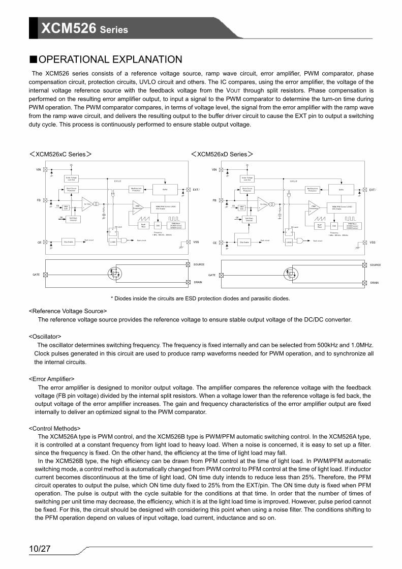
XCM526 Series The XCM526 series consists of a reference voltage source, ramp wave circuit, error amplifier, PWM comparator, phase
compensation circuit, protection circuits, UVLO circuit and others. The IC compares, using the error amplifier, the voltage of the internal voltage reference source with the feedback voltage from the VOUT through split resistors. Phase compensation is performed on the resulting error amplifier output, to input a signal to the PWM comparator to determine the turn-on time during PWM operation. The PWM comparator compares, in terms of voltage level, the signal from the error amplifier with the ramp wave from the ramp wave circuit, and delivers the resulting output to the buffer driver circuit to cause the EXT pin to output a switching duty cycle. This process is continuously performed to ensure stable output voltage.
<XCM526xC Series> <XCM526xD Series>
<Reference Voltage Source>
The reference voltage source provides the reference voltage to ensure stable output voltage of the DC/DC converter.
<Oscillator> The oscillator determines switching frequency. The frequency is fixed internally and can be selected from 500kHz and 1.0MHz.
Clock pulses generated in this circuit are used to produce ramp waveforms needed for PWM operation, and to synchronize all the internal circuits.
<Error Amplifier> The error amplifier is designed to monitor output voltage. The amplifier compares the reference voltage with the feedback
voltage (FB pin voltage) divided by the internal split resistors. When a voltage lower than the reference voltage is fed back, the output voltage of the error amplifier increases. The gain and frequency characteristics of the error amplifier output are fixed internally to deliver an optimized signal to the PWM comparator.
<Control Methods> The XCM526A type is PWM control, and the XCM526B type is PWM/PFM automatic switching control. In the XCM526A type,
it is controlled at a constant frequency from light load to heavy load. When a noise is concerned, it is easy to set up a filter. since the frequency is fixed. On the other hand, the efficiency at the time of light load may fall. In the XCM526B type, the high efficiency can be drawn from PFM control at the time of light load. In PWM/PFM automatic
switching mode, a control method is automatically changed from PWM control to PFM control at the time of light load. If inductor current becomes discontinuous at the time of light load, ON time duty intends to reduce less than 25%. Therefore, the PFM circuit operates to output the pulse, which ON time duty fixed to 25% from the EXT/pin. The ON time duty is fixed when PFM operation. The pulse is output with the cycle suitable for the conditions at that time. In order that the number of times of switching per unit time may decrease, the efficiency, which it is at the light load time is improved. However, pulse period cannot be fixed. For this, the circuit should be designed with considering this point when using a noise filter. The conditions shifting to the PFM operation depend on values of input voltage, load current, inductance and so on.
■OPERATIONAL EXPLANATION
PWM/PFM Control LOGIC OSC Enable
FBErr Amp
+
-
+
-VREF0.9V
Buffer EXT/
VIN
VSSCE Chip Enable
Soft Start(internal)
LOGICEach circuit
Under VoltageLock Out
Short CircuitProtection
MaxDutyLimitProtection
Ramp Wave
OSCRS Latch
R
S Q
CE
OE
Frequency :
1 MHz , 500 kHz , 300 kHz
Each circuit
PWM Wave(XC9221series)(XA9221series)
U.V.L.O
PWMComparator
SOURCE
GATE
DRAIN
SOURCE
GATE
DRAIN
PWM/PFM Control LOGIC OSC Enable
FBErr Amp
+
-
+
-VREF0.9V
Buffer EXT/
VIN
VSSCE Chip Enable
Soft Start(internal)
LOGICEach circuit
Under VoltageLock Out
Short CircuitProtection
MaxDutyLimitProtection
Ramp Wave
OSCRS Latch
R
S Q
CE
OE
Frequency :
1 MHz , 500 kHz , 300 kHz
Each circuit
PWM Wave(XC9221series)(XA9221series)
U.V.L.O
PWMComparator
* Diodes inside the circuits are ESD protection diodes and parasitic diodes.

11/27
XCM526 Series
<UVLO (Under Voltage Lock Out) > When the input voltage falls below 2.3V (TYP.), the external P-channel driver transistor is forced OFF. Once the UVLO
operates, the XCM526xC (soft-start internally fixed) resets the internal circuit. For this, by releasing the UVLO function, the IC performs the soft-start function to initiate output startup operation. As for the XCM526xD (soft-start set externally), when the input voltage falls because of a power cutoff and the IC stops operation due to the UVLO function, the IC resumes its operation by internal soft-start circuit. If the soft-start time is needed to set externally, the CE/CSS pin voltage should be reset to 0V. (Please see the soft-start circuit example.)
<Soft-Start Time> The XCM526xD types can adjust the soft-start time externally via the CE pin. The soft-start function operates until the CE pin
voltage becomes 2.6V. Please refer to the following equation for calculating the soft-start time. The soft-start time is depended on VCE, RSS and CSS. Minimum soft-start time is equal to the time set internally.
tSS= - CSS x RSS x In { (VCE – 2.2) / VCE }
■OPERATIONAL EXPLANATION (Continued)
●UVLO Operation
VIN
UVLO (InternalSignal)
VOUT(XCM526xCseries)
VOUT(XCM526xDseries)
U.V.L.O.release delay
Soft-start time: Tss1
U.V.L.O. operation
U.V.L.O.release delaySoft-start time
(Externally set-up):Tss2Soft-start time: Tss1
CE PIN
VCE
Rss
Css
CE PIN
VCE
Rss
Css
ON/OFFSignal
> Circuit Examle2 : CMOS logic (low current dissipation)
CE PIN
VCE
Rss
Css
ON/OFFSignal
> Cicuit Examle3 : CMOS logic (low current dissipation, quick off)> Circuit Example1 : N-ch Open Drain
CE PIN
VCE
Rss
Css
ON/OFFSignal
Internal soft-starttime: Tss1 (XCM526xCseries)
Externallyset soft-starttime:Tss2(XCM526xDseries)
Minimum soft-starttimeWhen externallyset :
Tss2_min = Tss1
XCM526xCseries
XCM526xDseries

12/27
XCM526 Series <Protection Circuits>
●Short-Circuit Protection Circuit (Latching Type) When the FB pin is shorted to Ground or the output voltage drops rapidly because of overload state, the P-ch driver
transistor is kept OFF. (The protection circuit operates when the FB voltage becomes 0.7V or lower.) For releasing the latching state, the circuit is needed to restart via the VIN or the CE pin.
■OPERATIONAL EXPLANATION (Continued)
●Short-circuit protection circuit
FB Voltage 0.9V
0.7V
VREF0.9V
Soft-start time : Tss × 90%
* Protection circuit does not operate.* About 100 to 200usec delay time is setto avoid latching when instantaneousTransient response drop
Less than 100usec = Not latching
Latch
100usec

13/27
XCM526 Series
1. For temporary, transitional voltage drop or voltage rising phenomenon, the IC is liable to malfunction should the ratings be exceeded.
2. The XCM526 series are designed for use with an output ceramic capacitor. If, however, the voltage difference between
input and output is too large, a ceramic capacitor may fail to absorb the resulting high switching energy and oscillation could occur on the output. If the input-output voltage difference is large, connect the output capacitor with large performance to compensate for insufficient capacitance.
3. Spike noise and ripple voltage arise in a switching regulator as with a DC/DC converter. These are greatly influenced
by external component selection, such as the inductance, capacitance values, and board layout of the external components. Once the design has been completed, verification with actual components should be done.
4. When the difference between input voltage and output voltage is large in PWM control, and the load current is light,
very narrow pulses will be output, and there is the possibility that some cycles may be skipped completely. 5. When the difference between input voltage and output voltage is small in PWM control, and the load current is heavy,
very wide pulses will be outputted and there is the possibility that some cycles may be skipped completely. 6. When using the CE pin by pulling up to the VIN pin, please be noted to the rising speed of the VIN pin voltage. If the
rising time of the VIN pin voltage is much slower than the soft-start time of the XCM526 series, the short-circuit protection starts to operate so that the output may not rise. When the VIN pin voltage rises slow, please use a voltage detector or something similar to check that the input voltage rises fully. After that, the IC can be started by using the CE pin. Or we recommend the XCM526xD, adjusting the soft-start period externally so that the voltage at the VIN pin rises fully before the soft-start period is completed.
7. Use of the IC at voltages below the minimum operating voltage may lead to instability. 8. This IC and external components should be used within the stated absolute maximum ratings. 9. Please do not use the XCM526 as the only Power MOSFET. 10. Torex places an importance on improving our products and its reliability.
However, by any possibility, we would request user fail-safe design and post-aging treatment on system or equipment.
Soft-Start Time(2msec (TYP.))@ Fosc=1MHz
VIN pin Voltage
FB pin Voltage
Releasing U.V.L.O.
Short-Protection Voltage: 0.7V(MAX.)
Rising time of the VIN pin voltage << Soft-Start Time
Rising time of the VIN pin voltage >> Soft-Start Time
Because the VIN pin voltage is low and the FB pin voltageis not reached to the short-protection voltage at the time thesoft-start time completes, the output turns out to be OFF bythe short-protection operation.
Short-protection function starts.
Normal Operation
■NOTES ON USE
14/27
XCM526 Series
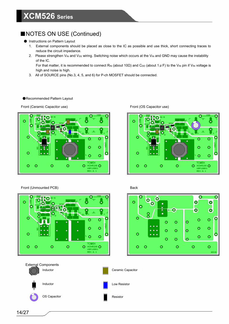
● Instructions on Pattern Layout 1. External components should be placed as close to the IC as possible and use thick, short connecting traces to
reduce the circuit impedance. 2. Please strengthen VIN and VSS wiring. Switching noise which occurs at the VIN and GND may cause the instability
of the IC. For that matter, it is recommended to connect RIN (about 10Ω) and CDD (about 1μF) to the VIN pin if VIN voltage is high and noise is high.
3. All of SOURCE pins (No.3, 4, 5, and 6) for P-ch MOSFET should be connected.
●Recommended Pattern Layout
Front (Ceramic Capacitor use) Front (OS Capacitor use)
Front (Unmounted PCB)
Back
External Components
■NOTES ON USE (Continued)
セラミックコンデンサインダクタ
ショットキー・バリア・ダイオード
OSコン
低抵抗器
抵抗器
Inductor
Inductor
OS Capacitor
Ceramic Capacitor
Low Resistor
Resistor

15/27
XCM526 Series
CIN:1μF
A
VSS
FB
VIN
CE
GATE
SOURCE
SOURCE
SOURCE
SOURCE
DRAIN
EXT/
A
CIN:1μF
VSS
FB
VIN
CE
GATE
SOURCE
SOURCE
SOURCE
SOURCE
DRAIN
EXT/
VA
VA
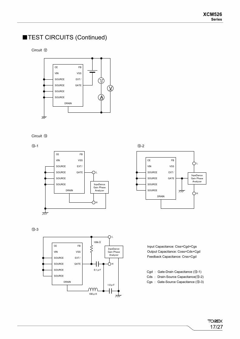
■TEST CIRCUITS Circuit ① Circuit ②
Circuit ③
Circuit ⑤
Circuit ④
CIN:1μF
VSS
FB
VIN
CE
GATE
SOURCE
SOURCE
SOURCE
SOURCE
DRAIN
EXT/
V V
Oscilloscope
CIN:1μF
VSS
FB
VIN
CE
GATE
SOURCE
SOURCE
SOURCE
SOURCE
DRAIN
EXT/
V V
200kΩ
0.1uF
Oscilloscope
VSS
FB
VIN
CE
GATE
SOURCE
SOURCE
SOURCE
SOURCE
DRAIN
EXT/
CIN:47μF
RFB1
RFB2
CL:47μF(OS-con)
V
A
CFB
L
SBD
L : 4.7uH(Fosc=1.0MHz)L : 10uH(Fosc=500kHz)
OscilloscopeRFB1 : 200kohmRFB2 : 75kohmCFB : 150pF

16/27
XCM526 Series
■TEST CIRCUITS (Continued)
Circuit ⑥
VSS
FB
VIN
CE
GATE
SOURCE
SOURCE
SOURCE
SOURCE
DRAIN
EXT/
←
V
Circuit ⑦
A
VSS
FB
VIN
CE
GATE
SOURCE
SOURCE
SOURCE
SOURCE
DRAIN
EXT/
Circuit ⑧
VSS
FB
VIN
CE
GATE
SOURCE
SOURCE
SOURCE
SOURCE
DRAIN
EXT/A
Circuit ⑨
VSS
FB
VIN
CE
GATE
SOURCE
SOURCE
SOURCE
SOURCE
DRAIN
EXT/A
Circuit ⑩
VSS
FB
VIN
CE
GATE
SOURCE
SOURCE
SOURCE
SOURCE
DRAIN
EXT/
V
A
Circuit ⑪
VSS
FB
VIN
CE
GATE
SOURCE
SOURCE
SOURCE
SOURCE
DRAIN
EXT/
V
A
17/27
XCM526 Series
VSS
FB
VIN
CE
GATE
SOURCE
SOURCE
SOURCE
SOURCE
DRAIN
EXT/
InpeDanceGain PhaseAnalyzer
H
L
100μH
1.0μF
0.1μF
100kΩ
■TEST CIRCUITS (Continued)
Circuit ⑫
Input Capacitance: Ciss=Cgd+Cgs Output Capacitance: Coss=Cds+Cgd Feedback Capacitance: Crss=Cgd
Cgd : Gate-Drain Capacitance (⑬-1) Cds : Drain-Source Capacitance(⑬-2) Cgs : Gate-Source Capacitance (⑬-3)
VSS
FB
VIN
CE
GATE
SOURCE
SOURCE
SOURCE
SOURCE
DRAIN
EXT/
H
L
InpeDanceGain PhaseAnalyzer
VSS
FB
VIN
CE
GATE
SOURCE
SOURCE
SOURCE
SOURCE
DRAIN
EXT/
H
L
InpeDanceGain PhaseAnalyzer
VSS
FB
VIN
CE
GATE
SOURCE
SOURCE
SOURCE
SOURCE
DRAIN
EXT/
V
A
Circuit ⑬
⑬-1 ⑬-2
⑬-3

18/27
XCM526 Series
■TEST CIRCUITS (Continued)
Circuit ⑭
0V
0V
VI
VO
10%
10%
90%
90%
td(on) td(off)tr tf
Circuit ⑮ Circuit ⑯
VSS
FB
VIN
CE
GATE
SOURCE
SOURCE
SOURCE
SOURCE
DRAIN
EXT/
Oscilloscope
50Ω
RL
VO
VI
VSS
FB
VIN
CE
GATE
SOURCE
SOURCE
SOURCE
SOURCE
DRAIN
EXT/
Oscilloscope
←
VSS
FB
VIN
CE
GATE
SOURCE
SOURCE
SOURCE
SOURCE
DRAIN
EXT/
V
A

19/27
XCM526 Series
■TYPICAL PERFORMANCE CHARACTERISTICS (1) Efficiency vs. Output Current
(2) Output Voltage vs. Output Current
(3) Output Ripple Voltage vs. Output Current
XCM526Ax/Bx9Axx
4.4
4.6
4.8
5.0
5.2
5.4
0.1 1 10 100 1000 10000
Output Current : IOUT (mA)
Outp
utV
oltag
e :
VO
UT
(V
)
SBD:CLS01, L=SLF10165T-4.7uH
CIN=22uF(ceramic), CL=47uF(ceramic), RSENSE=50mohm
VIN=12V => VOUT=5V
PWM(XCM526A)
PFM(XCM526B)
XCM526Ax/Bx9Axx
0
10
20
30
40
50
60
70
80
90
100
0.1 1 10 100 1000 10000
Output Current : IOUT (mA)
Effic
iency
: EFFI (%
)
SBD:CLS01, L=SLF10165T-4.7uH
CIN=22uF(ceramic), CL=47uF(ceramic), RSENSE=50mohm
VIN=12V => VOUT=5V
PWM(XCM526A)
PFM(XCM526B)
XCM526Ax/Bx9Axx
2.7
2.9
3.1
3.3
3.5
3.7
0.1 1 10 100 1000 10000
Output Current : IOUT (mA)
Outp
utV
oltag
e :
VO
UT
(V
)
SBD:CLS01, L=SLF10165T-4.7uH
CIN=22uF(ceramic), CL=47uF(ceramic), RSENSE=50mohm
VOUT=3.3V
VIN=5.0V
12V
PWM(XCM526A)
PFM(XCM526B)
XCM526Ax/Bx9Axx
0
20
40
60
80
100
0.1 1 10 100 1000 10000
Output Current : IOUT (mA)
Rip
pleV
oltag
e :
Vr
(mV
)
SBD:CLS01, L=SLF10165T-4.7uH
CIN=22uF(ceramic), CL=47uF(ceramic), RSENSE=50mohm
VIN=12V => VOUT=5V
PWM(XCM526A)
PFM(XCM526B)
XCM526Ax/Bx9Axx
0
10
20
30
40
50
60
70
80
90
100
0.1 1 10 100 1000 10000
Output Current : IOUT (mA)
Rip
pleV
oltag
e :
Vr
(mV
)
SBD:CLS01, L=SLF10165T-4.7uH
CIN=22uF(ceramic), CL=47uF(ceramic), RSENSE=50mohm
VOUT=3.3V
VIN=5.0V
PWM(XCM526A)
PFM(XCM526B)
VIN=12V
XCM526Ax/Bx9Axx
0
10
20
30
40
50
60
70
80
90
100
0.1 1 10 100 1000 10000
Output Current : IOUT (mA)Effic
iency
: EFFI (%
)
VIN=5.0V
PWM(XCM526A)
PFM(XCM526B)
VIN=12V
SBD:CLS01, L=SLF10165T-4.7μH
CIN=22uF(ceramic), CL=47uF(ceramic), RSENSE=50mohm
VOUT=3.3V
20/27
XCM526 Series
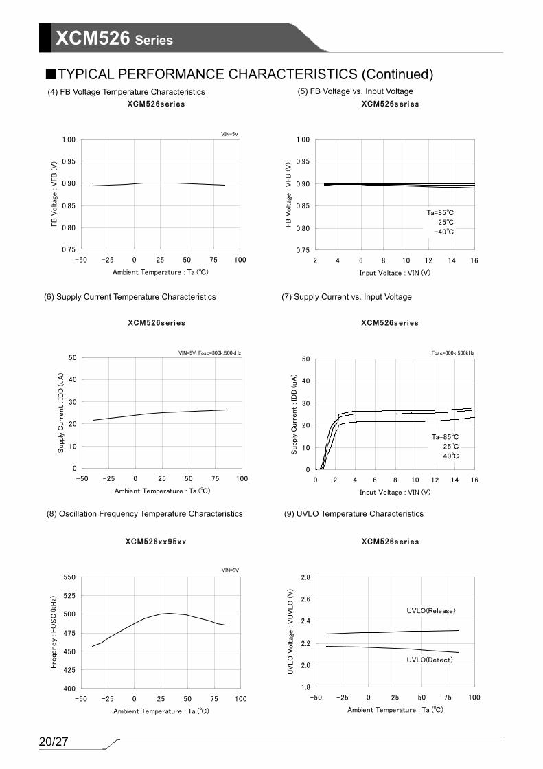
■TYPICAL PERFORMANCE CHARACTERISTICS (Continued) (4) FB Voltage Temperature Characteristics
(6) Supply Current Temperature Characteristics
(5) FB Voltage vs. Input Voltage
(7) Supply Current vs. Input Voltage
(8) Oscillation Frequency Temperature Characteristics (9) UVLO Temperature Characteristics
XCM526series
0.75
0.80
0.85
0.90
0.95
1.00
-50 -25 0 25 50 75 100
Ambient Temperature : Ta (℃)
FB
Voltag
e :
VFB
(V
)
VIN=5V
XCM526series
0.75
0.80
0.85
0.90
0.95
1.00
2 4 6 8 10 12 14 16
Input Voltage : VIN (V)
FB
Voltag
e :
VFB
(V
)
Ta=85℃
25℃
-40℃
XCM526series
0
10
20
30
40
50
-50 -25 0 25 50 75 100
Ambient Temperature : Ta (℃)
Supp
ly C
urr
ent
: ID
D (uA
)
VIN=5V, Fosc=300k,500kHz
XCM526series
0
10
20
30
40
50
0 2 4 6 8 10 12 14 16
Input Voltage : VIN (V)
Supp
ly C
urr
ent
: ID
D (uA
)
Fosc=300k,500kHz
Ta=85℃
25℃
-40℃
XCM526xx95xx
400
425
450
475
500
525
550
-50 -25 0 25 50 75 100
Ambient Temperature : Ta (℃)
Fre
qency
: FO
SC
(kH
z)
VIN=5V
XCM526series
1.8
2.0
2.2
2.4
2.6
2.8
-50 -25 0 25 50 75 100
Ambient Temperature : Ta (℃)
UV
LO
Voltag
e :
VU
VLO
(V
)
UVLO(Release)
UVLO(Detect)

21/27
XCM526 Series
■TYPICAL PERFORMANCE CHARACTERISTICS (Continued) (10) EXT H ON Resistance Characteristics (11) EXT L ON Resistance Characteristics
(12) Soft-Start Time Temperature Characteristics
(13) Integral Protection Time Temperature Characteristics
XCM526series
0
5
10
15
20
25
30
0 2 4 6 8 10 12 14 16
Input Voltage : VIN (V)
EX
T/H
Resi
stan
ce :
REX
TB
H (Ω
)
Ta=85℃
25℃
-40℃
XCM526series
0
5
10
15
20
25
30
0 2 4 6 8 10 12 14 16
Input Voltage : VIN (V)
EX
T/L R
esi
stan
ce :
REX
TB
L (Ω
)
Ta=85℃
25℃
-40℃
XCM526series
2.0
3.0
4.0
5.0
6.0
7.0
8.0
-50 -25 0 25 50 75 100
Ambient Temperature : Ta (℃)
Soft
-S
tart
Tim
e :
TS
S (m
sec)
VIN=5V, Fosc=300k,500kHz
XCM526series
1.0
1.5
2.0
2.5
3.0
3.5
4.0
-50 -25 0 25 50 75 100
Ambient Temperature : Ta (℃)
Soft
-S
tart
Tim
e :
TS
S (m
sec)
VIN=5V, Fosc=1.0MHz
XCM526series
0.3
0.4
0.5
0.6
0.7
0.8
-50 -25 0 25 50 75 100
Ambient Temperature : Ta (℃)
Short
-P
rote
ction V
oltag
e :
Vsh
ort
(V
) VIN=5V
XCM526series
0.3
0.4
0.5
0.6
0.7
0.8
0 2 4 6 8 10 12 14 16
Input Voltage : VIN (V)
Short
-P
rote
ction V
oltag
e :
Vsh
ort
(V
)
(14) Short-Circuit Protection Voltage vs. Input Voltage

22/27
XCM526 Series
XCM526series
0.0
0.2
0.4
0.6
0.8
1.0
1.2
0 2 4 6 8 10 12 14 16
Input Voltage : VIN (V)
CE V
oltag
e :
VC
EH
, VC
EL (V
)
CE_H
CE_L
XCM526series
0.0
0.2
0.4
0.6
0.8
1.0
1.2
-50 -25 0 25 50 75 100
Ambient Temperature : Ta (℃)
CE V
oltag
e :
VC
EH
, VC
EL (V
)
VIN=5V
CE_H
CE L
XCM526Ax95xx
VOUT=100mV/div., Time=50μs/div.
SBD : CLS01(TOSHIBA), L=10uH(RLF12545T, TDK)
CIN=47uF(ceramic), CL=47uF(OS-con)
VIN=5.0V, VOUT=3.3V
VOUT
IOUT
XCM526Ax95xx
SBD : CLS01(TOSHIBA), L=10uH(RLF12545T, TDK)
CIN=47uF(ceramic), CL=47uF(OS-con)
VIN=5.0V, VOUT=3.3V
VOUT=100mV/div., Time=10ms/div.
VOUT
IOUT
VOUT=100mV/div., Time=50μs/div.
XCM526Ax95xx
SBD : CLS01(TOSHIBA), L=10uH(RLF12545T, TDK)
CIN=47uF(ceramic), CL=47uF(OS-con)
VIN=10.0V, VOUT=3.3V
VOUT
IOUT
VOUT=100mV/div., Time=100ms/div.
XCM526Ax95xx
SBD : CLS01(TOSHIBA), L=10uH(RLF12545T, TDK)
CIN=47uF(ceramic), CL=47uF(OS-con)
VIN=10.0V, VOUT=3.3V
VOUT
IOUT
■TYPICAL PERFORMANCE CHARACTERISTICS (Continued) (15) CE Threshold Temperature Characteristics (16) CE Threshold vs. Input Voltage
(17) Load Transient Response Characteristics ・IOUT: 0.1mA → 1000mA
・IOUT: 300mA → 3000mA
23/27
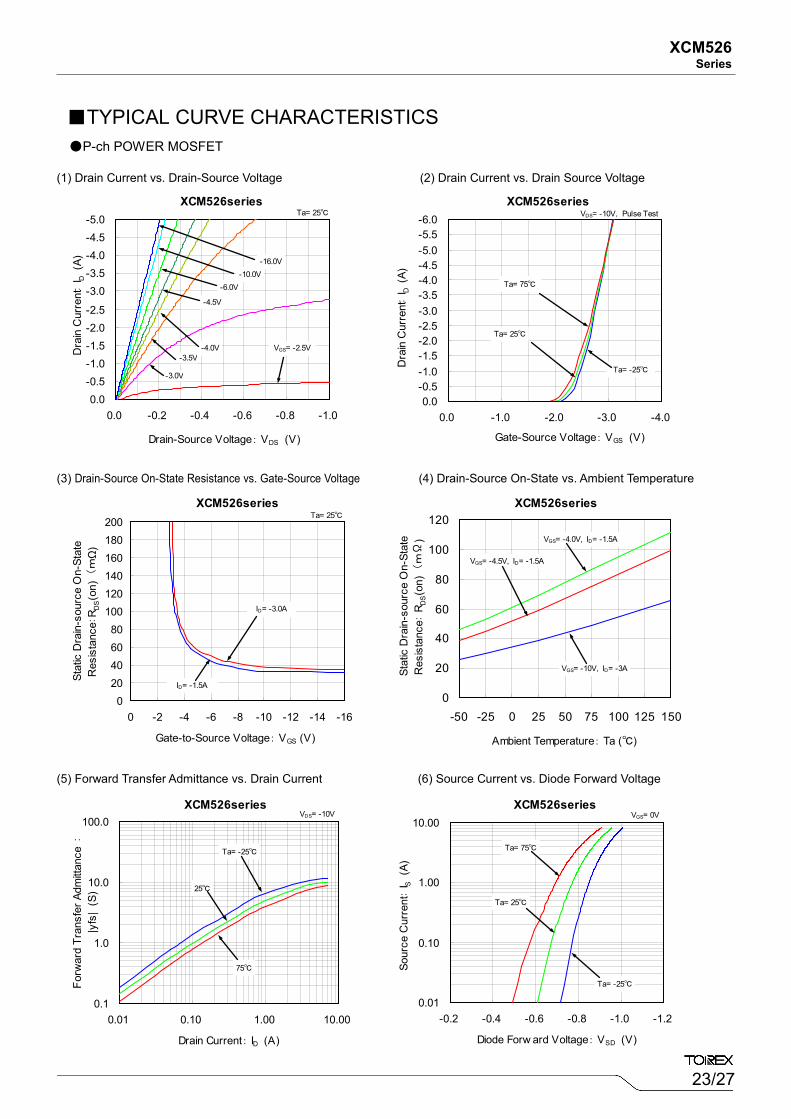
XCM526 Series
(1) Drain Current vs. Drain-Source Voltage (2) Drain Current vs. Drain Source Voltage (3) Drain-Source On-State Resistance vs. Gate-Source Voltage (4) Drain-Source On-State vs. Ambient Temperature (5) Forward Transfer Admittance vs. Drain Current (6) Source Current vs. Diode Forward Voltage
■TYPICAL CURVE CHARACTERISTICS ●P-ch POWER MOSFET
XCM526series-5.0-4.5-4.0-3.5-3.0
-2.5-2.0-1.5-1.0-0.50.0
-1.0-0.8-0.6-0.4-0.20.0
Drain-Source Voltage: VDS (V)
Dra
in C
urre
nt: I D
(A)
VGS= -2.5V
-3.0V
-3.5V-4.0V
-4.5V
-6.0V-10.0V
-16.0V
Ta= 25℃
XCM526series-6.0-5.5-5.0-4.5-4.0-3.5-3.0-2.5-2.0-1.5-1.0-0.50.0
-4.0-3.0-2.0-1.00.0
Gate-Source Voltage: VGS (V)
Dra
in C
urre
nt: I D
(A)
VDS= -10V, Pulse Test
Ta= 25℃
Ta= -25℃
Ta= 75℃
XCM526series
020406080
100120140160180200
-16-14-12-10-8-6-4-20
Gate-to-Source Voltage: VGS (V)
Stat
ic D
rain
-sou
rce
On-
Stat
eR
esis
tanc
e:R D
S(o
n) (
mΩ
)
Ta= 25℃
ID= -3.0A
ID= -1.5A
XCM526series
0
20
40
60
80
100
120
-50 -25 0 25 50 75 100 125 150
Ambient Temperature: Ta (℃)
Stat
ic D
rain
-sou
rce
On-
Stat
eR
esis
tanc
e: R
DS(o
n) (
mΩ
)
VGS= -10V, ID= -3A
VGS= -4.5V, ID= -1.5A
VGS= -4.0V, ID= -1.5A
XCM526series
0.1
1.0
10.0
100.0
0.01 0.10 1.00 10.00
Drain Current: ID (A)
Forw
ard
Tran
sfer
Adm
ittan
ce :
|yfs
| (S
)
Ta= -25℃
25℃
75℃
VDS= -10VXCM526series
0.01
0.10
1.00
10.00
-1.2-1.0-0.8-0.6-0.4-0.2
Diode Forw ard Voltage: VSD (V)
Sour
ce C
urre
nt: I S
(A)
Ta= 75℃
Ta= 25℃
Ta= -25℃
VGS= 0V

24/27
XCM526 Series
(7) Switching Time vs. Drain Current (8) Ciss, Coss, Crss vs. Drain-Source Voltage
(9) Gate-Source Voltage vs. Gate Charge
■TYPICAL CURVE CHARACTERISTICS (Continued) ●P-ch POWER MOSFET
XCM526series
1
10
100
0.1 1.0 10.0
Drain Current: ID (A)
Switc
hing
Tim
e: t
(ns)
td(on)
tr
td(off)
tf
VGS= -10V, VDS= -15VXCM526series
10
100
1000
0 5 10 15 20 25 30
Drain - Source Voltage: VDS (V)C
iss,
Cos
s, C
rss
(pF)
f=1MHz
Ciss
Coss
Crss
XCM526series
-10-9-8-7-6-5-4-3-2-10
0 1 2 3 4 5 6 7 8 9 10
Gate Charge: Qg (nc)
Gat
e-So
urce
Vol
tage
: V
GS (
V)
VDS= -15V, ID= -5A

25/27
XCM526 Series
■PACKAGING INFORMATION
For the latest package information go to, www.torexsemi.com/technical-support/packages
PACKAGE OUTLINE / LAND PATTERN THERMAL CHARACTERISTICS
USP-12B01 USP-12B01 PKG USP-12B01 Power Dissipation
26/27
XCM526 Series
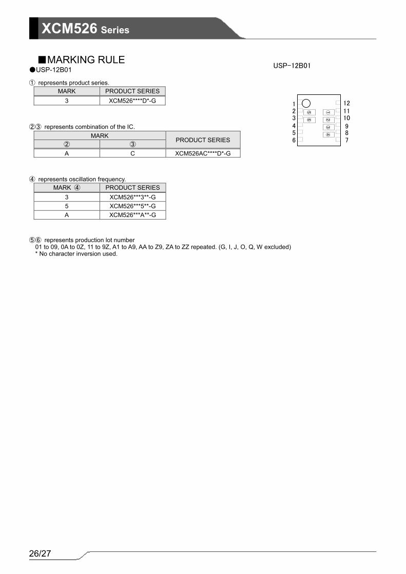
●USP-12B01
① represents product series. MARK PRODUCT SERIES
3 XCM526****D*-G ②③ represents combination of the IC.
MARK PRODUCT SERIES
② ③ A C XCM526AC****D*-G
④ represents oscillation frequency.
MARK ④ PRODUCT SERIES 3 XCM526***3**-G 5 XCM526***5**-G A XCM526***A**-G
⑤⑥ represents production lot number
01 to 09, 0A to 0Z, 11 to 9Z, A1 to A9, AA to Z9, ZA to ZZ repeated. (G, I, J, O, Q, W excluded) * No character inversion used.
■MARKING RULE
USP-12B01
123456
121110987
①②
③④
⑤⑥

27/27
XCM526 Series
1. The product and product specifications contained herein are subject to change without notice to improve performance characteristics. Consult us, or our representatives before use, to confirm that the information in this datasheet is up to date.
2. The information in this datasheet is intended to illustrate the operation and characteristics of our
products. We neither make warranties or representations with respect to the accuracy or completeness of the information contained in this datasheet nor grant any license to any intellectual property rights of ours or any third party concerning with the information in this datasheet.
3. Applicable export control laws and regulations should be complied and the procedures required
by such laws and regulations should also be followed, when the product or any information contained in this datasheet is exported.
4. The product is neither intended nor warranted for use in equipment of systems which require
extremely high levels of quality and/or reliability and/or a malfunction or failure which may cause loss of human life, bodily injury, serious property damage including but not limited to devices or equipment used in 1) nuclear facilities, 2) aerospace industry, 3) medical facilities, 4) automobile industry and other transportation industry and 5) safety devices and safety equipment to control combustions and explosions. Do not use the product for the above use unless agreed by us in writing in advance.
5. Although we make continuous efforts to improve the quality and reliability of our products;
nevertheless Semiconductors are likely to fail with a certain probability. So in order to prevent personal injury and/or property damage resulting from such failure, customers are required to incorporate adequate safety measures in their designs, such as system fail safes, redundancy and fire prevention features.
6. Our products are not designed to be Radiation-resistant.
7. Please use the product listed in this datasheet within the specified ranges.
8. We assume no responsibility for damage or loss due to abnormal use.
9. All rights reserved. No part of this datasheet may be copied or reproduced unless agreed by
Torex Semiconductor Ltd in writing in advance.
TOREX SEMICONDUCTOR LTD.