Feasibility of superconductivity in semiconductor superlatices
126
New Jersey Institute of Technology New Jersey Institute of Technology Digital Commons @ NJIT Digital Commons @ NJIT Dissertations Electronic Theses and Dissertations Summer 8-31-2006 Feasibility of superconductivity in semiconductor superlatices Feasibility of superconductivity in semiconductor superlatices Kenneth P. Walsh New Jersey Institute of Technology Follow this and additional works at: https://digitalcommons.njit.edu/dissertations Part of the Other Physics Commons Recommended Citation Recommended Citation Walsh, Kenneth P., "Feasibility of superconductivity in semiconductor superlatices" (2006). Dissertations. 792. https://digitalcommons.njit.edu/dissertations/792 This Dissertation is brought to you for free and open access by the Electronic Theses and Dissertations at Digital Commons @ NJIT. It has been accepted for inclusion in Dissertations by an authorized administrator of Digital Commons @ NJIT. For more information, please contact [email protected].
-
Upload
khangminh22 -
Category
Documents
-
view
2 -
download
0
Transcript of Feasibility of superconductivity in semiconductor superlatices

New Jersey Institute of Technology New Jersey Institute of Technology
Digital Commons @ NJIT Digital Commons @ NJIT
Dissertations Electronic Theses and Dissertations
Summer 8-31-2006
Feasibility of superconductivity in semiconductor superlatices Feasibility of superconductivity in semiconductor superlatices
Kenneth P. Walsh New Jersey Institute of Technology
Follow this and additional works at: https://digitalcommons.njit.edu/dissertations
Part of the Other Physics Commons
Recommended Citation Recommended Citation Walsh, Kenneth P., "Feasibility of superconductivity in semiconductor superlatices" (2006). Dissertations. 792. https://digitalcommons.njit.edu/dissertations/792
This Dissertation is brought to you for free and open access by the Electronic Theses and Dissertations at Digital Commons @ NJIT. It has been accepted for inclusion in Dissertations by an authorized administrator of Digital Commons @ NJIT. For more information, please contact [email protected].

Copyright Warning & Restrictions
The copyright law of the United States (Title 17, United States Code) governs the making of photocopies or other
reproductions of copyrighted material.
Under certain conditions specified in the law, libraries and archives are authorized to furnish a photocopy or other
reproduction. One of these specified conditions is that the photocopy or reproduction is not to be “used for any
purpose other than private study, scholarship, or research.” If a, user makes a request for, or later uses, a photocopy or reproduction for purposes in excess of “fair use” that user
may be liable for copyright infringement,
This institution reserves the right to refuse to accept a copying order if, in its judgment, fulfillment of the order
would involve violation of copyright law.
Please Note: The author retains the copyright while the New Jersey Institute of Technology reserves the right to
distribute this thesis or dissertation
Printing note: If you do not wish to print this page, then select “Pages from: first page # to: last page #” on the print dialog screen

The Van Houten library has removed some ofthe personal information and all signatures fromthe approval page and biographical sketches oftheses and dissertations in order to protect theidentity of NJIT graduates and faculty.
ABSTRACT
FEASIBILITY OF SUPERCONDUCTIVITYIN SEMICONDUCTOR SUPERLATIVES
by
Kenneth P. Walsh
The objective of this thesis is to explore superconductivity in semiconductor superlattice
of alternating hole and electron layers. The feasibility of superconductivity in
semiconductor superlattices is based on a model formulated by Horseman and Mills. In
this model, a semiconductor superlattice forms the layered electron and hole reservoirs of
high transition temperature (high-ΤΤ ) superconductors.
A GaAs—A1xGa 1_xAs semiconductor structure is proposed which is predicted to
superconductor at Cc = 2.0 K and may be analogous to the layered electronic structure of
high-Ta superconductors. Formation of an alternating sequence of electron- and hole-
populated quantum wells (an electron-hole superlattices) in a modulation-doped
GaAs—AlxGa 1_xAs superlattice is considered. In this superlattices, the distribution of
carriers forms a three-dimensional Wigner lattice where the mean spacing between
carriers in the x-y plane is the same as the periodic distance between wells in the
superlattices. This geometrical relationship mimics a prominent property of optimally
doped high — Cc superconductors.
A Schrδdinger-Poisson solver, developed by Snider, is applied to the
problem of determining the appropriate semiconductor layers for creating
equilibrium electron-hole superlattices in the GaAs—A1 xGa 1_xAs system. Formation of

equilibrium electron-hole superlatives in modulation-doped GaAs—A1 xGa 1_xAs is
studied by numerical simulations. Electron and heavy-hole states are induced by built-
in electric fields in the absence of optical pumping, gate electrodes, or electrical contacts.
The GaΑs—A1xGa 1_XAs structure and the feasibility of meeting all the criteria of the
Horseman model for superconductivity is studied by self-consistent numerical simulation.
In order to test the existence of superconductivity, the physics of sensor arrays
and their ability to create synthetic images of semiconductor structures, is explored.
Approximations are considered and practical applications in detecting superconductivity
in superlattices are evaluated.

FEASIBILITY OF SUPERCONDUCTIVITYIN SEMICONDUCTOR SUPERLATIVES
by
Kenneth P. Walsh
A DissertationSubmitted to the Faculty of the
New Jersey Institute of Technology andRutgers, the State University of New Jersey-Newark
in Partial Fulfillment of the Requirements for the Degree ofDoctor of Philosophy in Applied Physics
Federated Physics Department
August 2006

Copyright © 2006 by Kenneth P. Walsh
ALL RIGHTS RESERVED

APPROVAL PAGE
FEASIBILITY OF SUPERCONDUCTIVITYIN SEMICONDUCTOR SUPERLATIVES
Kenneth P. Walsh
Dr. Anthony Fiery, Dissertation Advisor DateResearch Professor of Physics, NJIT
Dr. Nuggehalli M. Ravindra, Dissertation Advisor DateProfessor of Physics, NJIT
Dr. Jo C. Hensel, Thesis Committee DateDistil fished Research ProfessεΡ9r of Physics, NJIT
Dr. Tao Chou, Thesis Committee ( DateAssistant Professor of Physics, NJIT
Dr. Chen Wu, Thesis Committee DateAssociate Professor of Physics, Rutgers University
Mr. Ma * ι Lepselter, Thesis Committee DatePresident, BTU Fellows, Inc.

BIOGRAPHICAL SKETCH
Author: Kenneth P. Walsh
Degree: Doctor of Philosophy
Date: August, 2006
Undergraduate and Graduate Education:
• Master of Arts in Physics,Queens College, Flushing, NY 1985
• Bachelor of Arts in Mathematics,Queens College, Flushing, NY 1972
Major: Physics
Presentations and Publications:
Walsh, KIP & Rajendran, Α.Μ. (1997). Modeling of in-situ ballistic measurements usingthe Rajendran-Grove and Johnson-Holmquist ceramic models. Proceedings of theShock Compression and Condensed Matter, AID Press, 913-916.
Walsh, KIP. (2000). Modeling the physical response of ceramics using a shock physicsbased code. Physics MS Thesis (unpublished), University of Maryland, Baltimore, MD.
Walsh, KIP., Schulkin, B., Gary, D., Federici, J. F., Bharat, R. & Zimdars, D. (2004).Terahertz near field interferometric and synthetic aperture imaging. Proceedings SPICE, Volume 5411, 1-9.
Walsh, KIP., Fiery, A. C., Ravindra, N. M., Horseman, D. R. & Dow, J. D. (2006).Feasibility of superconductivity in semiconductor superlattices.March APES Meeting Abstract/Presentation, Baltimore, MD.
Walsh, KIP., Fiery, A. T., Ravindra, N. M., Horseman, D. R. & Dow, J. D. (2006).Electron-Hole superlatives in GaΑs/Αl Ga1_ XΑs multiple quantum wells.Philosophical Magazine, Volume 86, Number 23, 3581 - 3593.
iv

Co the memory of my beloved cairn terrierCoto
1985-2001
"He gave so much and asked so little"
ν

ACKNOWLEDGEMENTS
I would like to express my deepest appreciation to Dr. Anthony Fiery and Dr. Nuggehalli
Ravindra, who not only served as my research supervisors, providing valuable and
countless resources, insight, and intuition but also constantly gave me support,
encouragement, and reassurance. Special thanks are given to Professors John Hensel,
Tao Chou, Chen Wu, and Martin Lepselter for actively participating in my committee.
Appreciation is extended to Dr. D. R Horseman of Physikon Research, Arizona
State University, and the University of Notre Dame and Dr. J. D. Dow of the Arizona
State University for their valuable support and collaboration. I appreciate the support of
Dr. Rao Surapeneni, Mr. Steven Nicolich and Mr. James Wejsa of the US Army at
Picatinny, NJ, who provided funding for my research efforts.
I am highly fortunate to have obtained an open source software program written
by Dr. Greg Snider of Notre Dame University. Without this program, my thesis research
would have been difficult or even impossible to accomplish.
Last, but not least, I am grateful to the helpful assistance of Catherine Allen, US
Army Librarian at Picatinny, NJ, who helped me obtain much of the background
literature used in this study.
vi

TABLE OF CONTENTS
Chapter Page
1 INTRODUCCION ... 1
1.1 Objective 1
1.2 High Temperature Superconductivity 3
1.3 Computer Modeling of Superlattice Nanostructures 8
2 CHEORY 12
2.1 BCC Theory of Superconductivity 12
2.2 The Horseman Formulation and Conditions for Superconductivity 12
2.3 Electron-Hole Formation in Superlattice GaAs-AIGaAs Wells .... 27
3 RESUUTS OF COMPUCER SIMULATIONS OF SUPERLATTICES 31
3.1 Sensitivity of the Electron-Hole Superlattices to Parametric Changes at LowTemperatures 31
3.2 The Effect of Donor Concentrations and Uayer Thickness on theBeta vs. T Plot 47
3.3 Superlattices with Uniform Spacing 53
3.4 Superlattices with Nonuniform Spacing and Delta Doping 59
4 RECENT DEVEUOPMENTS IN HIGH TEMPERATURESUPERCONDUCCIVICY . 60
4.1 Experimental and Theoretical Developments 60
5 CHE DETECTION OF SUPERCONDUCTIVITY USING SYNTHECICIMAGING 65
5.1 Synthetic Imaging. 65
5.1.1 General Principles 65
5.1.2 Coherence Function for Sensor Pairs on a Parabolic Array . 72
vii

TABLE OF CONTENTS(Continued)
Chapter Page
5.1.3 Coherence Function for Sensor Pairs on a Spherical Array 74
5.1.4 Coherence Function for Sensor Pairs on a Planar Array 76
5.2 Far Field Form of Phase Difference between Two Sensor Points ina Planar Array .. 77
5.3 Physical Structure of Near Fields Incident upon a Spherical Array 81
5.4 Synthetic Imaging Using an GIFT of a U-V File 84
5.5 Synthetic Imaging and the Detection of Superconductivity 90
6 CONCUUSIONS 97
APPENDIX A DERIVATION OF LOGARITHMIC DERIVATIVE OF THECRITICAL TEMPERATURE .. 98
APPENDIX B VALIDITY OF THE 3D HOLE/ELECTRON DENSITYFUNCTIONS AT THE T=0 K LIMIT .. 99
APPENDIX C THE 2-D INVERSE COURIER TRANSFORM (GIFT) OFTHE PRODUCT OF TWO DISPUACEMENT VECTORS ANDTHE CORRELATION FUNCTION 100
APPENDIX D DERIVATION OF THE CONDITION FOR NON-DISSIPATIONOF AN EM WAVE THROUGH A CONDUCTIVE MEDIUM......... 103
viii

LIST OF FIGURES
Figure Page
1.1 An example of a semiconductor superlative 2
1.2 The 2-D surface density vs. inverse square separation 6
1.3 Effect of magnetic field on resistance of a GaAs electron superlattice 7
1.4 Flowchart of the Snider computer program 9
1.5 Harrier and Thomas-Fermi plots of electron energy and density of carrier states. 11
2.1 Critical temperature vs. sheet carrier density 15
2.2 3D plot of argument of coulomb correlation vs. surface carrier density and
the Debby frequency 18
2.3 The energies for computer simulated noncrystalline structure (solid triangles)
and regular superlattice structures (open squares) 26
2.4 (a) The lowest energy structure has alternating infinite straightchains of ions at x = 0.4, (b) A zigzag structure at x = 0.4 ... 26
3.1 Semiconductor superlative and carrier formation . 33
3.2 Temperature dependence of sheet electron and hole densities calculated forthe modulation doped superlative for alloy concentration of x = 0.4 ... 34
3.3 Variation of well sheet electron and hole densities with concentration ofdeparts in modulation doped layers of a superlative for alloy concentration
of x = 0.4 .. 35
3.4 (a) Edges of conduction band, (b) Edges of valence band. For modulation dopedn-p-n superlative of alloy composition x = 0.4 as functions of
depth y (Case 3) ..... 40
3.5 Variation with depth y of the built-in electric field of a modulation dopedn-p-n superlattice of alloy composition x = 0.4 (Case 3) 41
3.6 (a) Edges of conduction band, (b) Edges of valence band. For modulation dopedn-p-n superlative of alloy composition x = 0.4 as functions ofdepth y (Case 4) 42
ix

LIST OF FIGURES(Continued)
Figure Page
3.7 Variation with depth y of the built-in electric field of a modulation dopedn-p-n superlative of alloy concentration x = 0.4 (Case 4) 43
3.8 Plots of acceptor areal density vs. d-delta.... 45
3.9 Plots of charge transfer efficiency vs. d-delta. 46
3.10 Quantum confinement in GaAs wells 47
3.11 Effect of layer thickness on beta 50
3.12 Effect of donor concentration on beta, L = 50 Angstroms 51
3.13 Beta vs. T (Case 1) 54
3.14 Beta vs. T (Case 2) ... 55
3.15 Beta vs. T (Case 4) .. 57
3.16 Beta vs. T (Case 5). . 59
5.1 (a) Near field wave fronts, (b) Far field wave fronts, (c) Geometry of arrayand source 67
5.2 (a) Far field wave fronts parallel to sensor plane, (b) Far field wave frontsat an angle to sensor plane
5.3 (a) planar array, (b) curved array
5.4 Geometry of sensor nodes and near field source .
5.5 Point source at d producing wave fronts at points 1,2 on the surface of aparabolic array
5.6 Point source at d producing wave fronts at points 1,2 on the surface of aspherical array .
5.7 Point source at d producing wave fronts at points 1,2 on the surface of aplanar array ..
68
71
71
73
75
76
χ

LIST OF FIGURES(Continued)
Figure Page
5.8 Source dB' irradiating a pair of sensors 78
5.9 Error delta from imaging 1.0, 2.0, 3.0 cm objects, frequency of radiation = 1.0terahertz .. 80
5.10 (a) Spherical sensor array and imaged object, (b) Spherical coordinate
system 83
5.11 Sensor nodes 1, 2 receiving radiation from a source point. .... 85
5.12 (a) Geometric arrangement of u-v 25 sensor nodes, (b) Nodes generated
in space by 25 sensors 86
5.13 (a) Circular geometric arrangement of 25 sensor nodes, (b) Nodes generatedin space by 25 circular sensors . 87
5.14 (a) Synthetic imaging of a source point with a spherical array, (b) Synthetic
imaging of a source point with a circular array 88
5.15 (a) Synthetic imaging of a source point with a spherical array, (b) Synthetic
imaging of a source point with a circular array 89
5.16 Circular array imaging sample in a cryostat 92
5.17 Scheme for determining superconductivity in a superlative using
a circular array 93
5.18 EM wave entering a semiconductor in superconducting state... 95
5.19 Reflectivity of LOCO as a function of the frequency for fixed impurityscattering rate with different temperatures 96
C.1 Geometry of source point and sensor nodes 101
xi

LIST OF TABLES
Table Page
3.1 Vary T (Case 1) 32
3.2 Vary Doping Concentrations, Beta (Case 2) 37
3.3 Effect of D-Delta on Sheet Resistance, Maximum Electric Field and ChargeTransfer Efficiency .. 38
3.4 Effect of D-Delta on Energy Band Offsets 38
3.5 Vary D-Delta, D-Spacer (Case 3) 39
3.6 Vary D-Delta, D-Well (Case 4) 44
3.7 Effect of Donor/Acceptor Concentration N and Layer Thickness L on Beta. 48
3.8 Relationships between the Electric Field and the Sheet Resistance as theLayer Thickness and Doping Concentrations are Varied ... 51
3.9 Effect of Donor and Acceptor Concentration N and Layer Width on Beta(Case 3) 56
5.1 Wavelength, Frequency and SR..... 91
xii

LIST OF SYMBOLS AND ACRONYMS
T, To temperature, temperature when β =1
mom hole effective mass, electron effective mass
n, p electrons, holes density (atoms/cubic centimeter)Tf-p, Tf-p Fermi temperature calculated from Νs,ΠsJ electron current densityd periodic distance between 2 hole or electron wells
beta, Psd2 , Psd2
SR spatial resolutionRs sheet resistance
P donor/acceptor concentration (atoms/cubic centimeter)EGG energy level difference between two adjacent wells
Cc conduction band energy
CC valence band energy
Ε conduction band energy in A1GaAs well
Εω conduction band energy in GaAs well
nano object object whose dimensions are measured in Angstromsmacro object object whose dimensions are measured in millimeters or
centimetersPs surface electron density
Pssurface hole density
D( ΕΙ ) density of states for energy Εί
A AngstromSC superconductingλα electron-phonon coupling coefficient
ΗΕ hole-exciton coupling coefficient
Coulomb correlation coefficientAL lateral resolutionx alloy concentration in AIXGaι_XAsεχ dielectric constant of A1 χGa1_χAsL layer thickness in Angstroms
Mx ,d-spacer spacing between ND± and NA layers in A1 χGa 1 _χAsdB ,dwell width of the undated GaAs wells
d8 ,d-delta width of the dated A1 χGa 1 _χAs layers.Bs width of the substrate
do width of the cap

ΝΑΙ acceptor concentration for layer I (atoms/cubic centimeter)
ND1 donor concentration for layer I (atoms/cubic centimeter)
AD , Bp ionized donor, acceptor densities (atoms/cubic centimeter)dye mesh size
SE Schr5dinger EquationΨ wavefunctionp charge density (per cubic centimeter)En total energy of a particle
BEGS GaAs energy band gap in the superlative
Eros maximum induced electric field a superlative can tolerate
ΕΜ maximum induced electric filed within a superlative
nm manometerι Ec OFF / Δdδ change of conduction band offset with respect to d 8
ΔEv OFF / d8 change of valence band offset with respect to d8
HAS high temperature superconductivity1-D one dimension2-D two dimensions3-D three dimensionsV(k) potential difference between adjacent wells as a function of
wavenumber kbeta-p beta associated with an electron distributionbeta beta associated with an hole distribution
e-eigen electron eigenvalueh-eigen hole eigenvalue
Νς prefactor in the electron density of states relation
(2(2πm*kΒT/h2)2/3 )ND prefactor in the hole density of states relation
(2(2πm* kΒT/h2)2/3 )
kJ Boatsman's constant
CA acceptor atom ionization energy
ED donor atom ionization energy
EM electromagneticΕ electric fieldB magnetic fieldEx same as 10x
σα surface electric field density
m metercm centimetermm milimeterSC superconductivity
GIFT Inverse Fourier Transform
Div

CHAPTER 1
INTRODUCTION
1.1 Objective
The purpose of this study is to determine the structure and physical properties of
semiconductor superlattices that exhibit superconductivity at high temperatures. In order
to investigate this, GaAs-ΑΙ Ga 1 _χAs superlattice structures are utilized. A two-
dimensional layered geometry of high critical temperature (high-ΤΤ ) superconducting
materials is optimized both for T and the bulk Meissner fraction [1]. The proposed
superlattice structure comprises multiple repeating undoped GaAs and doped or undoped
AIXGa 1 _XAs layers which are analogous to the layered electronic structure of
high-Ρ superconductors. In the structures of interest, when the system is in a state of
electrostatic equilibrium, the mean spacing between nearest electron or hole wells is the
same as the mean distance between the electrons or holes in any given well. A computer
program is applied to the problem of determining the appropriate semiconductor layers
for creating equilibrium electron-hole GaAs-Αl Ga1_ XAs superlattices.
Computer simulations are based on a superlattice structure as seen in Figure 1.1.
The superlattice is composed of layers of undoped GaAs layers, doped and undoped
A1GaAs layers. The periodic distance d is the distance between GaAs wells surrounded
by like doped A1GaAs. Numerically, one can express the periodic distance as
d = 2(2dδ + d + dy ) , where d8, dB, and dX are the widths of the doped, well, and spacer
layers, respectively. The program uses the method of finite differences to find the
1

2
one-dimensional band diagram of a semiconductor structure. It can automatically
calculate the band diagrams for multiple bias voltages, sheet resistance, and surface
carrier densities. A self-consistent 1D solution of the Schrδdinger and Poisson Equations
is obtained using the finite-difference method (FDM) [2]. FDM divides real space into
meshes and mesh points. The vector solution of Schrδdinger Equation is solved for each
mesh. The result is a matrix formulation of the solution of the Schr6dinger Equation. The
method is very effective in determining eigenstates over a relatively large spatial
dimension without loss of accuracy. The program is menu driven through a pseudo-Mac
interface but the user must provide separate text editing and plotting programs. The
program calculates the conduction and valence band distributions, density of states and
the hole and electron concentrations. Depart ionization is included for both shallow and
deep level departs. This allows materials such as semi-insulating GaAs to be treated.
Current flow is not calculated; therefore, the structure can be simulated only in
thermodynamic equilibrium.
Figure 1.1 An example of a semiconductor superlative.

3
1.2 High Temperature Superconductivity
The complexity of high temperature superconductivity brings together expertise from
materials scientists, physicists and chemists, experimentalists and theorists to understand,
demonstrate, and interpret these phenomena. Much of the research in
high-Τc superconductivity has generated other areas of research where complex materials
play an important role. The materials could consist of magnetism in the manganese,
complex oxides, and two and one-dimensional magnets. Studies of superconductors
seems to indicate that the higher the T^ the more complex the material. There has been a
considerable effort to find universal trends and correlations amongst physical quantities
(superfluid density, conductivity, and the critical temperature) as a clue to the origin of
the superconductivity. One of the earliest patterns that emerged was the linear scaling of
the superfluity density with the superconducting transition temperature, which marks the
onset of phase coherence. However, it fails to describe attimally dated (where C c is a
maximum) or overrated materials [3].
Theoretical approaches face challenges in identifying a clear avenue for
interpreting empirical studies in which material parameters and praterties are correlated
with superconducting praterties [4]. Comparisons of theoretical ideas, which rely only on
artificially engineered layered superlattices, will be explored in this study.
The discovery of new superconducting high-Tc cuprates in 1986 by Bednorz and
Mueller has played an important role in the advancement of the field of superconductivity
research since its inception [5-8]. In MgB 2 superconductors, it was discovered that an in-
plane boron phonon mode, that modulates lattice constants and angles within the
honeycomb lattice, is responsible for coupling to the conduction electrons and is

4
the driving force for superconductivity [9]. The modulation of the bond lengths by
phonon modes may create distortions in the Wigner lattice that is formed in superlattices
after tunneling, thus creating a potential distribution, which may be the mechanism for
super current at high temperatures. Studies of novel quantum phases in an unexplored
regime of system dimensions and parameters, and nanoscale high-temperature
superconducting structures will allow exploration of fundamental mechanisms with
unprecedented insight [10]. High-temperature superconductivity in the nanometer scale
from the perspective of experiments, theory, and simulation are currently being
explored. It is the nanoscale of superconductivity that is the main focus of this study.
Despite the large number of studies and extensive research conducted since the
discovery of high-Tc superconductivity in the 1980's, the numerous theories and
formulations that have been pratosed over the years have not been satisfactory in
explaining high temperature superconductivity.
A more recent formulation by Harshman, which is an unpublished theoretical
work in progress, considers the attimal structure for superconductivity as having
alternating layers of hole-carrying and electron-carrying sheets. The Harshman and Mills
[11] formulation for the presence of superconductivity is defined by the parameter
β = P s d2 or β = psd 2, where Ps and Ps are the surface carrier densities and d is the
spacing between hole or electron layers. When β = 1, the condition for maximizing T^
occurs. The condition β = 1 occurs when the mean distance between charge carriers
within the sheets equals the distance d between the sheets. Harshman and Mills [1]
studied the properties of all the experimental data on high-T c superconductors which
allowed for dynamic charge screening and confinement. The superconductors were

5
analyzed in terms of layered two-dimensional conducting sheets with Coulomb coupling
between the sheets (Figure 1.2). They recognized that high —Τc materials have (solid line
in Figure 1.2) β = Nsd2 = Psd2 =1.0. It was later noted that alternating carrier layers
within the material may be present separated by a periodic distance d that also
satisfies β = N sd2 = Psd2 =1.0.
Co test this possibility, Harshman and Mills [11] prepared an n-dated GaAs
superlattice sample but no signs of superconductivity were present. The resistance,
however, was dependent on both temperature and external magnetic fields. The magnetic
field affected the slate of the resistance vs. temperature curves as shown in Figure 1.3.
At about 3 K, the resistance was field independent. Anomalous curves existed when the
magnetic intensity was 4 and 6 Tesla. Even though there was no direct evidence of SC, a
`shadow' of SC was evident in the fact that magnetic fields affect the resistance.
Harshman [12] hypothesized that if a material is both p-dated and n-dated, the
formation of alternating carrier layers may induce SC. The alternating carrier layers may
trap holes and create a hole distribution that could cause super current.
Alternating layers of hole-carrying and electron-carrying sheets can be described
as a Wigner lattice. The lattice is one in which charges on lattice sites interact via a
Coulomb interaction in a uniform background of atposite charge, such that there is
overall charge neutrality. A Wigner crystalline form for electrons may appear at low
electronic densities [13] and it may be energetically feasible for the stationary ions to
form a distorted periodic lattice. A distortion creates potential wells in which electrons
are trapped in and form a Wigner electron crystal. Together, the periodic bunching of the
positive ions and the trapped electrons form a periodic charge density variation. This and

6
holes trapped by them. Holes create vacancies and high-Τ superconductivity occurs
thesis postulates that the periodic potential is the result of a coupling between excitons
when the number of vacancies exceeds a certain threshold. If a superlattice nanostructure
satisfies the criteria for the Harshman and Mills formulation for attimum
superconductivity defined by the parameter β =1, then the structure is essentially a 3-D
Wigner lattice in electrostatic equilibrium. The Wigner lattice forms at carrier densities
that are attimized for superconductivity.
Figure 1.2 The 2-D surface density vs. inverse square separation. The circles representlayered materials that might exhibit HAS. Solid circles have unambiguous geometries andattimized parameters; aten circles have ambiguous geometries or insufficient data. (fromFigure 10 in Reference 11).
The kinetic energy of the electrons in a Wigner lattice in the low-density limit
becomes negligible and the charges arrange themselves resulting in the minimization of
the electrostatic energy. The presence of elastic and magnetic effects in real
compounds can strongly modify the predicted ordering pattern and the ratio of intraplanar

7
Coulombic interactions to kinetic energy [14]. Covalent bonding in a 2-D well
confinement gives electrons fewer ways of avoiding each other. Strongly interacting
electrons tend to maximize their relative distance and minimize their electron energy
configuration by forming crystals.
The feasibility of constructing a semiconductor superlattice that obeys the
Harshman formulation for superconductivity is examined in this study. Ongoing research
in electron-hole pair condensation and the formation of "ghost" hole layers and the
consequent coupling in relation to the Harshman formulation, will be discussed [15].
Electron-hole pair condensation, in addition to the strong Coulombic coupling of carrier
sheets, may be a contrary factor in achieving equal carrier layers in a superlattice.
"Ghost" holes may be the holes trapped by excitons discussed in a later section.
Figure 1.3 Effect of magnetic field on resistance of a GaAs electron superlattice.

8
1.3 Computer Modeling of Superlattice Nanostructures
In this study, a series of computer simulations were performed to determine the structure
and praterties of a superlattice when β for pairs of hole/electron wells is between 0.5
and 2. The program employed in the superlattice simulations is a 1-D FORTRAN
program develated by Dr. Greg Snider of Notre Dame University [ 16]. Later, a C version
was employed that increased the number of mesh points by two orders of magnitude, thus
reducing the occurrence of nonconvergence. Computer simulations are based on an
iterative process using Schrbdinger-Poisson solvers in which an initial wave function is
estimated and the wave function is updated for each cycle (Figure 1.4) until convergence
is achieved. The final resulting wave function is utilized to calculate the charge
distribution.
The program uses a method of finite differences [ 17] in one-dimension to create
profiles of semiconductor structures for temperatures in the range of 4-300 K.
Schrbdinger-Poisson (S-P) solvers can be employed for cryogenic temperatures. The
drawback is that using the S-P solvers for simulations below 50 K can cause problems
with convergence. At what temperatures the S-P solvers attion could be discarded is
determined later in this section.
The program calculates the conduction and valence bands and the hole and
electron concentrations. Dopant ionization is included for both shallow and deep level
datants. Current flow is not calculated and hence the structure can be simulated only in
thermal equilibrium. Three possible boundary conditions can de defined for the surface
and the substrate: Schottky barrier, Ohmic contact and slope = 0.
A Schottky barrier is defined at the surface or substrate where the default

9
barrier height is the barrier of the adjacent semiconductor with the attion of
specifying an applied bias. The Ohmic specifier sets the difference of the conduction and
Fermi energy levels (Εc —EF) at the boundary to the value required for charge neutrality
at the boundary. Slate = 0 sets the slate of the bands equal to zero at the boundary. If a
Schottky barrier is used, the program can simulate the effect of an applied bias, which
does not cause significant current flow. One can assign different Fermi levels to layers in
the biased structure as a way of simulating structures under bias. This can be done only if
the current flow is small enough to be ignored. If an Ohmic contact boundary condition is
specified, the applied bias must match the Fermi level in the adjacent layer. The slate = 0
boundary condition is used when only a certain region of interest is to be simulated.
Figure 1.4 Flowchart of the Snider computer program.

10
For the superlattices used in the simulations, one can expect significant band
bending if the dating is in a wider bandgap material. The band bending is tied to charge
density in the wells, and one affects the other. The band bending will also affect charge
transfer between wells. 1 D Poisson calculates the band diagram based on dating and
boundary conditions. Thus it inherently calculates the band bending.
Poisson's Equation relates the electrostatic potential to the charge distribution, but
is useful by itself only with explicit knowledge of the charge distribution. When
augmented by assumptions relating the charge density to the electrostatic potential, a
screening equation can be derived. Universal electrostatic behavior in such situations is
that the charges tend to move so as to reduce the magnitude of the electric field.
Calculating the charge density from the bulk density of states and with the assumption of
a local quasi-equilibrium described by Boltzmann statistics leads to Debye screening.
Using the bulk density of states with Fermi-Dirac statistics, the result is Thomas-Fermi
screening. Without utilizing the bulk density of states, but using the bound states from the
Schrδdinger Equation, and weighing them by a Fermi-Dirac distribution, results in a
Hartree screening. Hartree calculation is the same as a "Schrbdinger-Poisson solver". In
a modulation-dated structure, this sort of calculation is useful when applied in the
epitaxial growth direction for determining the surface carrier density. It is not usefully
applied in the transport direction because the unbounded scattering solutions of the
Schr idinger Equation have an "anti-screening" behavior, which prevents convergence to
any meaningful results.
Modeling of heterostructures has indicated that one usually has to go to cryogenic
temperatures in order to see a significant difference in the results. The plots at 10 K are
shown in Figure 1.5. The figures show comparisons of Hartree (left) and Thomas-Fermi

11
(right) screening in an undated AlGaAs-GaAs heterostructure at a temperature of 10 K.
The green lines show the energy and approximate spatial distribution of the quantized
states. The boundary between the A1GaAs and GaAs is the vertical black line. To the left
is GaAs and to the right is AlGaAs. The charge distribution due to the evanescent tails of
the wave functions is apparent in the Hartree case. In the plots, note that the potential
reaches a deeper minimum in the Hartree case, because the lowest electron state lies at an
energy well above the bottom of the potential well. Since there is no significant
difference between the Hartree and Thomas-Fermi screening for T > 10 K, one can "turn
off' the S-P attion down to just above T=10 K if convergence problems occur.
Figure 1.5 Hartree and Thomas-Fermi plots of electron energy and density of carrierstates.

CHAPTER 2
THEORY
2.1 BCS Theory of Superconductivity
Bardeen-Coater-Schrieffer (BCS) theory is a comprehensive theory that explains the
behavior of superconducting materials. The theory successfully explains the ability of
certain metals at low temperatures to conduct electricity without resistance. BCS theory
views superconductivity as a macroscatic quantum mechanical effect. It pratoses that
electrons with atposite spin can become paired; creating two bound electrons called
Coater pairs. BCS theory states that the binding of Coater pairs is a result of the
electron-phonon interaction, which causes an attraction between electrons, thus
overcoming the Coulomb repulsion. During the electron-phonon interaction, phonon
energy can be gained or lost by the electron. Since the difference of the incident and
scattered wave vectors of the electrons are not equal to a reciprocal lattice vector, the
scattering amplitude is less than maximum thus increasing the degree of forward
supercurrent. The electron-phonon interaction temporarily binds electrons in a lattice and
supplies a means by which the energy required to separate the Coater pairs into their
individual electrons can be measured experimentally.
The Coater pairs are formed when an electron moving through a conductor
causes a slight increase in concentration of positive charges in the lattice around it; this
increase in turn can attract another electron. In effect, the two electrons are then held
together with a certain binding energy. If this binding energy is higher than the energy
provided from oscillating atoms in the conductor, then the electron pair will stick
together, thus not experiencing resistance. Since the electrons are bound into Cooper
12

13
pairs, a finite amount of energy is needed to break these apart into two independent
electrons indicating an energy gap which separates the Coater electron pairs after
superconductivity vanishes. This energy gap is highest at low temperatures but
vanishes at the transition temperature when superconductivity ceases to exist.
Conventional superconductors are materials that display superconductivity as
described by the BCS theory for its extensions. Mercury was the first conventional
superconductor and was discovered at the beginning of the last century. Most
conventional superconductors are single elements or binary alloys. Their critical
temperatures are low but some binary alloys have a critical temperature up to 23 K [18].
2.2 The Harshman Formulation and Conditions for Superconductivity
The high temperature superconductors were first discovered in 1986 by Bednorz and
Mueller [ 19] and continue to pose very fundamental questions for Condensed Matter
physicists to address. Seemingly, they are not likely candidates for superconductors, since
basically they are insulators. However, by adding charge carriers by chemically dating
them, they become superconductors with transition temperatures of up to 135 K, which is
well below room temperature but is very high for a quantum mechanical state to
dominate the praterties.
The Hubbard model can be employed as an approximation to describe the
transition between conducting and insulating systems. The Hubbard Model is a
commonly used approximation for the behavior of electrons on a lattice that assumes an
onsite-only repulsive interaction and allows hatping between adjacent sites.
Investigations into the Hubbard model arise from the catper-dioxide planes including
the oxygen atoms, and find important departures from the behavior of the Hubbard

14
model. In the low dating limit, a quantum paramagnet is stabilized, and not a
ferromagnet. The Hubbard model can explain asymmetry in the electron- and hole-dated
phases, since the electron dated materials are necessarily described by the Hubbard
model [20].
Α fundamental mechanism for superconductivity arises from the interaction of a
hole with the outer electrons in atoms with nearly filled shells. Superconductivity results
from the pairing of hole carriers, and is driven by the fact that paired holes can propagate
more easily (have a smaller effective mass) than single holes with a lower kinetic energy.
Single electrons pratagate freely and do not pair. Dynamic Hubbard models describe the
different physical phenomenon of electron and hole carriers in metals. The reason for the
increased mobility of holes upon pairing is that they 'undress' when they pair, and turn
into electrons. This leads to a new understanding of superconductors which considers a
superconductor as a giant atom and implies that the electron-phonon interaction is not a
factor in HAS superconductivity and the BCS theory is not applicable.
The theory of superconductivity asserts that superconductivity can only occur
when hole carriers exist in the normal state of a metal. The formation of holes is the
key mechanism for superconductivity, since holes resulting from unfilled covalent bonds
do not repel as electrons do. There is a difference between electrons and holes in energy
bands in solids from a many-particle point of view, originating in the electron-electron
interaction and it has fundamental consequences for superconductivity. The difference
between electrons and holes parallels the difference due to electron-electron interactions.
Superconductivity may originate in 'undressing' of carriers [21]. Electrons at the Fermi
surface give rise to high conductivity and normal metallic behavior. Holes at the Fermi

15
surface yield poor conductivity and give rise to superconductivity [22].
In order to test for superconductivity when the Coulombic hole-exciton coupling
correlation factor is dominant, it has been suggested to test a 2-dimensional electron gas
produced in a GaAs superlattice. The hole-exciton coupling is a hypothetical mechanism
which occurs when holes are trapped by excitons and may be the source of supercurrent
at high temperatures. Excitons form as a result of alternating carriers layers in a
superlattice.
Figure 2.1 Critical temperature vs. sheet carrier density. The sketch is qualitative andrepresents the concept behind experimental findings and pratosals of the Harshman andMills analysis of titration experiments.
Harshman and Mills [23] suggested that layered high-Tc superconductors have
alternating sheets of holes and electrons whose net charge must be equal to zero to
preserve charge neutrality. It was deduced, from observations on experimental data, that a
sketch could be used to show the relationship between Tc and β or between Τ and
P. is pratortional to the Fermi Energy E F , in a 2-D system since T d / λL,

16
square of λs . Knowing the surface hole density for β = 1.0, the London penetration
depth can be calculated.
In addition to using the results of computer simulations to test the
superconducting hypothesis in superlattices, this thesis will pratose a novel theoretical
understanding of the Harshman Model and how it connects to BCS theory. Α trial
function, containing a new coupling other than the electron-phonon coupling, will be
utilized in the next sections to explain the Harshman sketch in Figure 2.1.
For a layer with a surface charge density N, the average near neighbor distance in
the x and y directions between atoms is 1 / ‚jΖ. If two layers with surface charge density
N are separated by d, then the near neighbor spacing in the x, y, and z directions within
the layers equals d and β = Nd 2 = 1. If alternating layers of carriers are coupled and
separated by d, carriers will redistribute themselves so as to minimize the resultant
electric field on each carrier. This geometry is the structure that is associated with the
Wigner 3-D lattice at temperature Ρ .
In most cases, it is unphysical to assume the existence of strong attractive
interactions which indicates the presence of a weak Coulomb correlation.
Coulombic correlation suggests that a 2-D Wigner lattice must exist in layers within the
semiconductor material. Α 2-dimensional electron gas between layers within a
superlattice is the criterion for the formation of a Wigner lattice. The correlation to HAS
and conventional BCS theory is discussed in the following sections.
The formulation β = 1.0 for maximal T is an observational equation that
suggests that the dominant interaction is a Coulombic interaction, which is in contrast to
the predominant electron-phonon correlation λΕ and Coulombic interaction μ for BCS

17
superconductivity. Layers of coupled alternating holes and electrons may contain the
indirect excitons which could capture holes. In BCS theory, the positive charge
distribution is caused by the distortion of the lattice structure by incident electrons. The
positive charge distribution in the Harshman formulation may result from the
accumulation of holes within excitons which in turn causes supercurrent.
Bardeen-Coater-Schrieffer (BCS) theory postulates that the predominant mode of
interaction in a Coater pair is the electron-phonon correlation in which the critical
temperature Tc is obtained from:
Phonons can distort the local crystal lattice and the local band structure. The conducting
electrons are "sensed" by the lattice distortion [24].
However, for high-Tc , the electron-phonon coupling is too weak to explain the
formation of Bosonic states from electron Fermions at high temperatures, but phonon
renormalization cannot be entirely discarded in explaining HAS. Phonon renormalization
is still important since phonons are within the critical energy range in the binding of
Coater pairs via charge fluctuations [25]. Electron-phonon coupling strongly influences
the electron dynamics in high temperature superconductors and should be included in any
microscatic theory of superconductivity [26].
Hypothetically, one could, however, explain the nature of the sketch qualitatively
using conditions and equations derived from low—T BCS theory by replacing the
electron-phonon coupling λΕ with another term λΗE resulting from another mechanism.
The mechanism may involve the trapping of holes by indirect excitons.

18
• As β increases (Figure 2.1), more holes may be trapped by indirect excitons. The
source of the trapped holes may be the positive charge distribution caused by the
electron-phonon interaction and the periodic positive charge distribution inherent in a
Wigner lattice. The density of the trapped holes and λ ΗΕ reaches a maximum at β = 1
since the net electrostatic forces on all charges, including the holes within the excitons,
are at a minimum.
According to renormalization group (RG) theory, the Coulomb correlation is
calculated by multiplying the interaction strength by the density of states and the
renormalized value is [27]:
where EF = P s π/ 2 /m*. Using m* = 0 . 1 5χ9. lxi kg, h = 6.62Χ10 -34 joules-sec,
the argument in the log component of the equation above is 0.00242 NS/wD. A varying
wD can affect the T^ so phonon modes can influence the critical temperature.
Figure 2.2 3D plot of argument of coulomb correlation vs. surface carrier density and theDebye frequency.

19
Decreasing 0D can promote the value of the critical temperature since μ*
decreases as log[Νsπh/(m*ωD ] increases. In Figure 2.2, log[P sπh/(m*ωD] has an
upward slate that assumes a greater positive value as Ν s increases from
10χ10 10 —100χ1010 carriers cm 2 and as 0D decreases from 100x10 8 —1χ108 sec-1 .
However, from points 1-2 in Figure 2.1, the near neighbor distances decrease as β
increases. Therefore, μ* is an increasing function of β . This would require that 8) D
increases faster than P s. As 0D increases, the first factor in Τ c increases but an
increasing wD in the exponential function of the second factor in Τc would tend to have
a much greater effect in decreasing Τ. When β varies from 0.5 to 2.0 in the Harshman
sketch, the rates of change of λΗΕ , wD and μ* determine how Tc advances.
If the Coulomb correlation μ* is dominant (λ ΗΕ - μ* <0), then the instantaneous
interaction is repulsive. According to standard RG analysis, when hω υ < kJTc , the weak
coupling estimate of the pairing scale Tc is kJTc hwD exp[-1/(λΗΕ - μ*)]. As P s
increases from point 1 to point 2 on the Harshman sketch, λ Hα and exp[-1/(λΗΕ - μ *)]
may both increase since the indirect excitons, formed as a result of the charges layers, are
capturing more holes and thereby promoting the hole-exciton coupling. A maximal point
for Tc is reached at point 2 when a change in P s results in a reduced Τ. In order for
Tc to be at a maximum at point 2, there are several possible conditions. The
following conditions to be satisfied are the most probable:
ωD (2) > 0D (1), λΗΕ (1) < λΗΕ (2), μ*(1) < μ*(2), dλΗΕ /dβ > dμ* /dβ, dwD /dβ > dPs /dβ .

20
The dependence of T on wD can be shown to be: (see Appendix A)
If hωπ < kΒΤςexp[—(1— λΗΕ ) /(λχεμ)] , d log[kJT^ ] / d log[k BωD] - 1.0, then the critical
temperature ΤΤ is a linearly increasing function of w D in the region between
points 1 and 2 on Harshman sketch. When hwD > kBΤΤexp[1/μ*], ΤΤ becomes a
decreasing function of wD in the region between points 2 and 3 on the
Harshman sketch.
According to Harshman formulation, superconductivity exists when β lies
between 0.5 and 2.0. At β = 0.5 (point 1 in Figure 2.1), ΤΤ is at its minimum and near-
neighbor distances of the carriers are at a maximum. At β = 1.0 (point 2 in Figure 2.1),
the electrostatic interactions are at a minimum and the carriers are equally spaced. In
addition, the electrostatic forces on all hole carriers captured by excitons are balanced.
The number of Bosonic pairs and captured holes could now be maximal due to the
alignment of excitonic pairs. When β = 2.0, ΤΤ and near-neighbor distance of the
carriers at a minimum, but now the and their interactions in the x-y plane are at
maximum and again in a state of electrostatic nonequilibrium.
The Harshman model postulates that, in order to exhibit HAS, a superlattice
design must satisfy certain condition according to the model. In designing a functional
GaAs-AIGaAs superlattice, the preferable superlattice structure must have
the following praterties: (1) β is equal to 1 at T = 0 K. (2) The maximum tolerable
electric field ΕΜ in the superlattice is less than limit of Eros = 5χ105 V/cm
and a maximum sheet resistance of R s = 104 Ohms. (3) Ν s and Ps are about equal. (4)
21
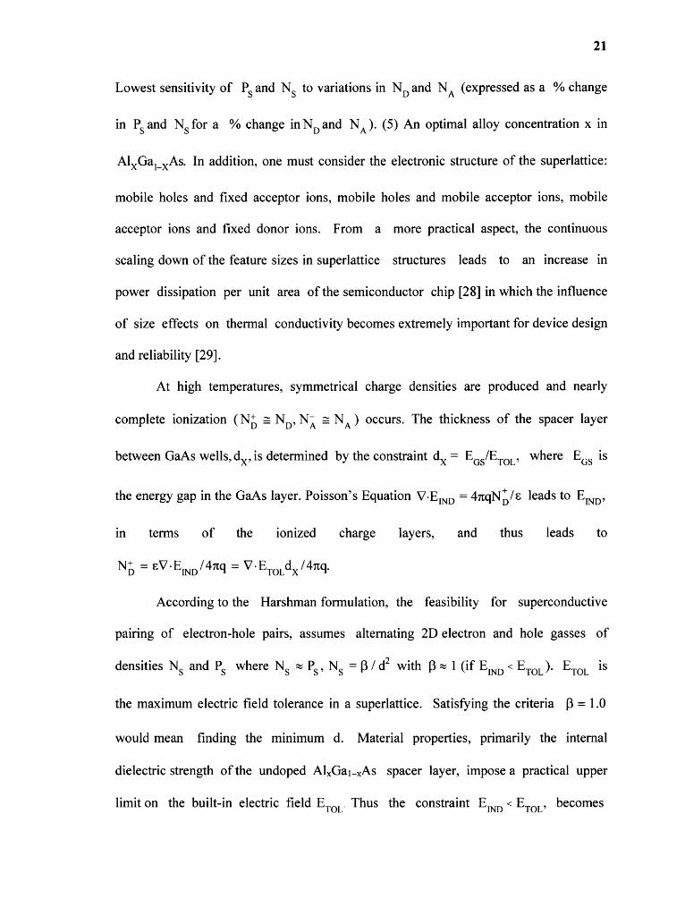
Lowest sensitivity of Ps and Ps to variations in ND and PΑ (expressed as a % change
in Ps and Νs for a % change in N D and PΑ ). (5) An attimal alloy concentration x in
A1xGa 1_xΑs. In addition, one must consider the electronic structure of the superlattice:
mobile holes and fixed acceptor ions, mobile holes and mobile acceptor ions, mobile
acceptor ions and fixed donor ions. From a more practical aspect, the continuous
scaling down of the feature sizes in superlattice structures leads to an increase in
power dissipation per unit area of the semiconductor chip [28] in which the influence
of size effects on thermal conductivity becomes extremely important for device design
and reliability [29].
At high temperatures, symmetrical charge densities are produced and nearly
between GaAs wells, dx , is determined by the constraint dX = EGS/Eros, where EGS is
the energy gap in the GaAs layer. Poisson's Equation V.E11vD = 4πqP /ε leads to E1r^D,
in terms of the ionized charge layers, and thus leads to
According to the Harshman formulation, the feasibility for superconductive
pairing of electron-hole pairs, assumes alternating 2D electron and hole gasses of
the maximum electric field tolerance in a superlattice. Satisfying the criteria β = 1.0
would mean finding the minimum d. Material praterties, primarily the internal
dielectric strength of the undoped Al χGa 1 _χAs spacer layer, impose a practical upper
limit on the built-in electric field Eros. Thus the constraint Ε11vD < Eros, becomes

22
induced electric field on the surface of the carrier layers if d x is kept constant.
The superconducting transition temperature can be calculated from the Fermi
energy of the 2D electron gas, EF = πh2Νs /m and Τc = β3Ε / kB , where
β3 =0.267-0.359 and mÉ is the electron effective mass. The variation of
β3 (0.267-0.359) is necessary since the calculated Τc must be consistent with the
formula for the critical temperature as is given at the end of this paragraph. It is assumed
at this point that the expression, above, for the critical temperature can be applied for
alternating carrier layers as well as superconductors with a periodic distance of d. The
maximum critical temperature can now be estimated: Tc = 1. lxi Ο4β/(md2 ) where d is in
Angstroms and me is the effective mass coefficient. If d = 800 Angstroms and if
m = mÉ / m0 = 0.06 , which is the approximate effective mass coefficient for AIGaAs,
then Tc = 1.8-2.4 K. This is a lower Figure than in the cuprates, for example, because a
minimum value of dX is determined by how great a field in the spacer can be
tolerated. Tc is inversely proportional to the inverse square of d. The very magnitude of d

23
sets an upper limit on the superconducting transition temperatures. Superconducting
transition temperatures are also estimated from the expression
eigenvalues. This T is a generalization to strong coupling (A ~ 2 — 3) and is consistent
with experiments on high—Ta superconductors.
The Harshman sketch (Figure 2.1) is qualitative and is based on observational
data and must be consistent with Tc a 1/mς . The sketch itself cannot be taken as
completely accurate since T must be close to zero at points 1 and 3, corresponding to β
= 0.5 and 2.0 respectively. This implies that the effective masses at these points must be
orders of magnitudes greater than at point 2 when β = 1.0. Until
recently, for dated semiconductors, decreases in the layer thickness of the superlattice
has resulted in a small reduction of the effective mass by a few percentage points [31].
Cleaved-edge overgrowth techniques, however, have led to structures with twice the
effective electron mass in two-dimensions [32]. Effective masses in ΥbΑ1 3 can be
shown to be dependent on magnetic fields and disorder, [33] and to what extent
magnetic fields and disorder can promote the critical temperature by reducing the
effective masses of holes and electrons remains uncertain.
The evolution of hole and electron densities may differ given identical
parameters if certain conditions are met (Section 2.3). There may be numerous factors
that contribute to the difference between the formation of holes and electrons. One factor
is that tunneling of holes and electrons differ because they have different effective
masses and mobilities. Another factor is the geometry and design of a superlattice.

24
Electrons flowing into the GaAs wells surrounded by n-dated AlGaAs form more
slowly because the accumulating electron buildup within the well restricts further
increases in the free electron density. Electrons flowing out of the GaAs wells
surrounded by p-dated AlGaAs have hole densities that form more rapidly because
the electronic outflow is directed away from the well in two directions and tunnel
throughout the entire superlattice and whose accumulations are not highly localized.
Hole densities evolve differently than electron densities, making it difficult to achieve
equal and alternating carrier densities, one of the criteria of the Harshman formulation.
The ternary value of A1GaAs may adversely affect tunneling during ionization.
The problem may be due to physical mechanisms and/or due to limitations in the Snider
program. As the alloy concentration decreases, the electrostatic energy configuration of
the Al and GaAs ions increases, making the system more disordered. This causes a
"roughness" at the boundary of the A1GaAs/GaAs interface. When ionization energy is
transferred at the Fermi level, the results may be a huge increase in the carrier
concentration. The superlattice structure that is being simulated is very sensitive to the
surface and substrate boundary conditions because it is nearly charge neutral with respect
to the fixed charge. For low x, if electrons form in the first and last well, holes form
in the central wells to balance this negative charge. The wells are too shallow to get
carriers in alternating wells. By contrast, in the x = 0.4 case, the wells are deep enough to
get carriers in alternating wells.
Given two kinds of ions, Al χGaAs I _ χ interacting via Coulomb interactions within
the plane, the problem is to determine how the ions, and hence the carriers, are arranged
on a 2D lattice at different concentrations. The long range Coulomb interaction couples

25
all pairs of ions and it is not possible to obtain analytic calculations. Thus, one must
resort to computer simulations.
Despite the difficulties in determining the exact nature of a Wigner
lattice, computer simulations using the Monte Carlo method, together with simulated
annealing, can be used to ascertain the minimum energy configuration for a 2-D
triangular lattice (Figure 2.3), alternating straight chains (Figure 2.4 a) or a zigzag
structure (Figure 2.4 b). At a given alloy concentration x, the structures are chosen
initially at random at a high initial temperature. For a state of lowest energy, x takes
on a value of 0.4 for infinite long chains and a value of 0.5 for a zigzag structure. The
ternary used in the simulations for this study was 0.4. Choosing a ternary greater than 0.4
leads to increased overlapping and offsets of the valence and conduction energy bands.
There are two general classes of nonrandom structures and are symmetric about
the concentration x = 1/2 as shown in Figure 2.4. For x < 1/3, like ions stay apart at
a maximum distance and hence form a dilute triangular lattice at low x. This is effectively
a Wigner lattice and the energetics of the 2D Wigner lattice with a continuum
background for charge neutrality agree very well with simulation results at small x.
According to Harshman's hypothesis, Tc can be increased if there are equal and
alternating layers of electrons and holes. At β = 1, the electrons and holes in a
superlattice are equally spaced in all directions and hence are in a state of minimum
electrostatic equilibrium. A minimum electrostatic energy configuration of Al and GaAs
ions before ionization and for carriers after ionization, are correlated with equal and
alternating carrier layers — one of the criteria of the Harshman model for SC.

26
Figure 2.3 The energies for computer simulated noncrystalline structures (solid triangles)and regular superlattice structures (aten squares) (from Figure 9 in Reference 30). Thecharges in the triangular lattice is e and the lattice spacing is a.
Figure 2.4 (a) The lowest energy structure has alternating infinite straight chains of ionsat x = 0.4 (from Figure 7 in Reference 30), (b) Α zigzag structure at x = 0.5 (from Figure8 in Reference 30).

27
2.3 Electron-Hole Formation in Superlattice GaAs-AIGaAs Wells
Consider a GaAs well surrounded by two dated A1GaAs barriers. The n and p densities
in three dimensions can be expressed as follows:
where mAlGaAs' mGaas are the electron effective masses in A1GaAs and GaAs wells,
respectively.
For low and high temperatures, substituting E F above into Equations 2.4 and 2.5,
yields an expression for density of holes and electrons. Factors other than effective
masses influence carrier evolution. For holes, the wavenumber is a factor in the hole
density, whereas for electrons it is not. Hole evolution is also affected by differences
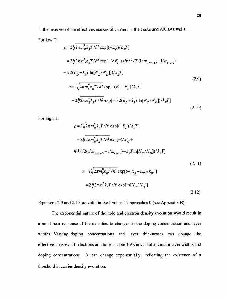
in the inverses of the effectives masses of carriers in the GaAs and A1GaAs wells.
Equations 2.9 and 2.10 are valid in the limit as T approaches 0 (see Appendix B).
The exponential nature of the hole and electron density evolution would result in
a non-linear response of the densities to changes in the dating concentration and layer
widths. Varying dating concentrations and layer thicknesses can change the
effective masses of electrons and holes. Table 3.9 shows that at certain layer widths and
dating concentrations β can change exponentially, indicating the existence of a
threshold in carrier density evolution.

29
Since k = nπ / L, where L is the layer thickness, as L increases, k decreases. As
the layer thickness increases or decreases from Equation 2.6, the potential difference
between adjacent wells V(k) may decrease or increase, depending upon the effective
masses change. Thus, more or fewer electrons can tunnel out of the GaAs well. As more
or less electrons tunnel from the GaAs well into the p-dated AlGaAs as a result of the
varying V(k), positive ionic cores are created or disappear. The result causes the drag or
pull on the electrons in the well and thus affecting the effective mass. A small change in
the term 1/mΑ1GaAs —1/m GaAs can greatly affect the density of hole states and thus β
changes. Changing hole density and keeping temperature constant can lead to a change in
the slate of β vs. temperature. Since β is Ρ sd2 , the ratio of sheet hole densities at points
1 and 2 on β vs. T curves, at some specified temperature, is given by β 2 /βι•
The increase in β with increases in donor concentrations can be explained as
follows. When two semiconductor layers are in contact, the occupation probability Ρ for
an electron of energy Ε ί in semiconductor i is Ρ(Ε) = f(Ε 1 ) = 1/[(eχρ(Ε ί —μ)/kΡΙ + 1)
where f(E 1 ) is the Fermi-Dirac distribution function. The density of electron states in
semiconductor i is n 1 . The product of the two is the density of available states.
Let the difference in energy levels of two semiconductors be V, so
Ε2 = Ε1 + V, where Ε 1 and Ε2 are the energies of the electrons in semiconductors 1 and 2
respectively. In semiconductor 2, the rate of tunneling R(Ε 2) into semiconductor
1 is directly pratortional to the number of unoccupied states in semiconductor 1. By
Fermi's Golden Rule, it is R(Ε 2 ) a IΜI 2 [1 — f (Ε 1 )]η 1 (Ε 1 ), where ρ(Ε 1 ) is the density
of available hole states in semiconductor 1 at energy Ε 1 and Μ is the tunneling

30
amplitude. The value of ρ(E 1 ) is the product of the density of electron states and the
probability that an electron state is unoccupied and is given by ρ(E 1 )=[1—f(E 1 )]n 1 (E 1 ).
Thus the rate of tunneling from semiconductor 2 into semiconductor 1 as a function of
the electron's energy Ε 1 is R(Ε 2 ) αc IΜI 2 [1— f (E 1 )]n 1 (E 1 ).
The total number of electrons at energy Ε 2 in semiconductor 2 that might tunnel
is n 2 (Ε2 )f (Ε2 ) , where n 2 is the density of electron states in semiconductor 2. The
tunneling of electrons from semiconductor 2 to semiconductor 1 is pratortional to the
product of the density of available holes in semiconductor 1 (ρ(Ε 1 ) = [1 —f(Ε 1 )]n 1 (Ε 1 ))
and the density of electrons in semiconductor 2. Integrating over all possible energies E,
the current from 2 to 1 is:
where K is a constant that depends on junction geometry.
CHAPTER 3
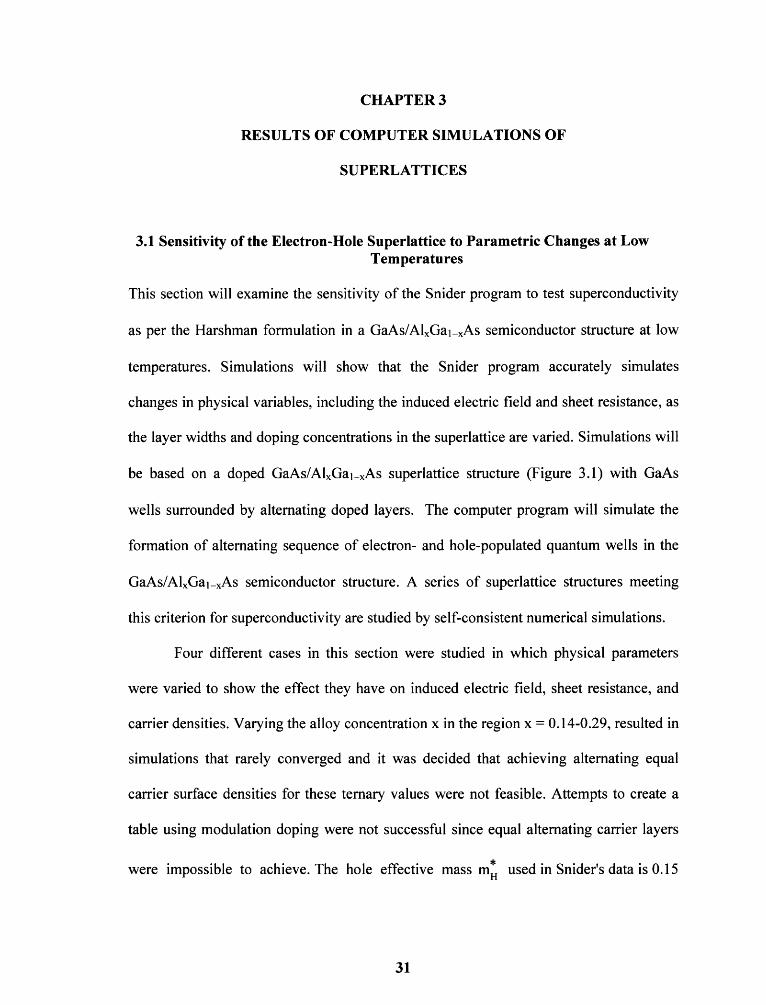
RESULTS OF COMPUTER SIMULATIONS OFSUPERLATIVES
3.1 Sensitivity of the Electron-Hole Superlative to Parametric Changes at LowTemperatures
This section will examine the sensitivity of the Snider program to test superconductivity
as per the Horseman formulation in a GaAs/A1 χGa1_χAs semiconductor structure at low
temperatures. Simulations will show that the Snider program accurately simulates
changes in physical variables, including the induced electric field and sheet resistance, as
the layer widths and doping concentrations in the superlative are varied. Simulations will
be based on a doped GaAs/A1 χGa1_χAs superlattice structure (Figure 3.1) with GaAs
wells surrounded by alternating doped layers. The computer program will simulate the
formation of alternating sequence of electron- and hole-populated quantum wells in the
GaAs/Αl Ga I _χAs semiconductor structure. A series of superlattice structures meeting
this criterion for superconductivity are studied by self-consistent numerical simulations.
Four different cases in this section were studied in which physical parameters
were varied to show the effect they have on induced electric field, sheet resistance, and
carrier densities. Varying the alloy concentration x in the region x = 0.14-0.29, resulted in
simulations that rarely converged and it was decided that achieving alternating equal
carrier surface densities for these ternary values were not feasible. Attempts to create a
table using modulation doping were not successful since equal alternating carrier layers
were impossible to achieve. The hole effective mass mú used in Snider's data is 0.15
31

32
m0 (the electron rest mass), which is the most accurate value measured by cyclotron
resonance for AIGaAs grown epitaxially in the (311) plane [36]. In the following tables
and plots, CGS units are used, energies are in electron volts and layer widths are in
Angstroms.
Table 3.1 Vary T (Case 1)

33
The superlattice structure that is being simulated is very sensitive to the surface
and substrate boundary conditions because it is nearly charge neutral with respect to the
fixed charge. Another issue is that the ionization of dopants at very low
temperatures (especially 0 K) is complicated. The x = 0.4 structure is more likely to
have electrons and holes in the wells because the wells are deeper compared to the depth
of the surrounding A1GaAs layers. This effect can be pronounced at 0 K because the
Fermi function is very abrupt. If electrons form in the last well, holes form in the central
wells to balance this negative charge. For x < 0.3, the wells are too shallow to get
both positive and negative carrier distributions in alternating wells. By contrast in the x
= 0.4 case, the wells are deep enough to get positive and negative carriers in alternating
wells.
Figure 3.1 Semiconductor superlattice and carrier formation.
The Snider program has limitations, and has difficulty calculating datant ionization at
low temperatures. If one assumes a single ionization energy in the bandgap for dopants,

34
the carriers should freeze out at low temperatures. This alone causes numerical
problems as the abrupt Fermi function leads to large changes in charge
concentration as the Fermi level exceeds the ionization energy. Α single depart energy
ignores the depart energy bands caused by degenerate dating. Particularly at low
temperatures, the program has a hard time converging if it does not have at least one
fixed boundary condition. Schrδdinger's and Poisson's Equations are solved self-
consistently in a region, if one specifies the boundaries of the region, measured from the
surface.
Figure 3.2 Temperature dependence of sheet electron and hole densities calculated forthe modulation doped superlative for alloy concentration of x = 0.4.
In Case 1 (Table 3.1), temperature changes had significant effect on the induced
electric field. The sheet resistance decreased as the temperature rose but only
incrementally. Ionization increased with increasing temperature. Both the surface charge
densities and Fermi energies increased as expected with increased ionization. The sheet

Figure 3.3 Variation of sheet electron and hole densities with concentration of departsin modulation doped layers of a superlative for alloy concentration of x = 0.4.
In Case 2 (Table 3.2), the layer widths were held constant as was x and T, while
NA, ND and β were varied. Progressively increasing the doping concentration by

36
3.48% resulted in a large decrease in the sheet resistance and a large increase in β ,
charge surface densities and the Fermi energy - consistent with theory. As PΑ and ND
increased from 1.2051019 to 1.244χ1 019 atoms/cm 3 (Cable 3.2), the sheet resistance
decreased by 98.4%. Che induced electric field increased by 1% and the ratio ρ / P Dd8
increased by over 5,900%. Che efficiency of charge transfer to the quantum wells are
calculated as ΥΙΕ = nd /PDd8 for the electrons or 11H = pdu /PDd8 for the holes.
Changes in Ε with respect to changes in doping can be expressed as Δη Η = βαAP and
ΔΕΗ = CHAP and their plots are shown in Figure 3.3 with C HI = CC = 960 cm 3 .
In Case 3 (Cable 3.5), the width of the doped and spacer layers varied but β , the
width of the well, and x were kept fixed with constant C = 0 K. Since β was held
constant, the charge surface densities and the Fermi energy remained virtually unchanged
as did the conduction and valence profiles (Figure 3.4). As d 8 increased from 1.0 to 5.5
nm, the sheet resistance decreased by 46.7%, the induced electric field increased by
23.4% (Figure 3.5), and the ratio PDd8 decreased by 20.2% (Cable 3.3).
Conduction and valence band edges offsets (Figure 3.4) at d8 = 5.0 and 3.0 nm in
the GaAs wells cross the Fermi level at -58.5 and 6.1 reV, respectively, with no change
in the offsets as d 8 was varied (see Cable 3.5). For Case 3, the change in the induced
electric field increased by 23.4 % as d8 was varied. In contrast, for Case 4, the change in
the induced electric field decreased by 2.4 % as d8 was varied (Cable 3.3). Che larger
electric field increase in Case 3 was the result of the spacer being reduced in width as the
width of the doped layers increased. Decreasing the width of the spacer layers increases
the threshold of the induced field causing fewer carriers to be transferred into the GaAs

37
wells. The result is an induced electric field having a higher concentration outside the
GaAs wells. The conduction and valence band edges in the GaAs wells remain
constant for incremental increases in d 8 . Figure 3.5 shows the built-in electric field
E(y) as a function of depth coordinate y for the same simulation results that
Table 3.2 Vary Doping Concentration, Beta (Case 2)

38
produced Figure 3.4. The magnitude of the field is maximum and nearly constant in the
spacer layers. The electric field in the GaAs wells increases by 22.8 mV/cm per nm
incremental increase in d8 .
Table 3.3 Effect of D-Delta on Sheet Resistance, Maximum Electric Field and ChargeTransfer Efficiency
In Case 4 (Table 3.6), the width of the dated and well layers were varied while
the spacer was held constant at 240 Angstroms. The charge surface densities, β and
the Fermi energy remained virtually unchanged. As the width of the well increased, d 8
had to be decreased in order to maintain a constant d. Since M x remained
constant, the threshold field within the spacers also remained constant. As d 8 increased
from 10 to 55 Angstroms, the sheet resistance decreased by 51.7%, the induced electric
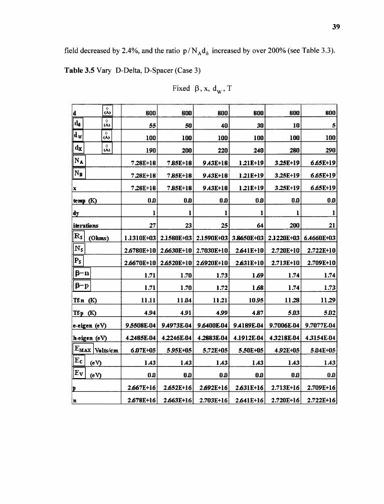
39
field decreased by 2.4%, and the ratio p/ NDd8 increased by over 200% (see Table 3.3).
Table 3.5 Vary D-Delta, D-Spacer (Case 3)

40
Figure 3.4 (a) Edges of conduction band, (b) Edges of valence band. For modulationdoped n-p-n superlative of alloy composition x = 0.4 as functions of depth y (Case 3).

41
Conduction and valence band edges offsets (Figure 3.6) at d8 = 5.0 and 3.0 nm
in the GaAs wells cross the Fermi level at -234, -59, and 6.6, 6.6 meV, respectively,
with only the conduction band offset increased as d B was varied. The conduction band
edge in the GaAs wells increases by 87.5 meV per nm incremental increase in d B . The
valence band edge in the GaAs wells remained constant as dB varied. Figure 3.7
shows the built-in electric field Ely) as a function of depth coordinate y for the same
simulation that resulted in Figure 3.5. The magnitude of the field is maximum and
nearly constant in the spacer layers owing to the unchanged threshold field. The electric
field in the well in the GaAs wells increases by 6.6 mV/cm per nm incremental increase
in dB .
Figure 3.5 Variation with depth y of the built-in electric field of a modulation doped n-p-n superlative of alloy composition x = 0.4 (Case 3).

42
Figure 3.6 (a) Edges of conduction band, (b) Edges of valence band. For modulationdoped n-p-n superlative of alloy composition x = 0.4 as functions of depth y (Case 4).

Figure 3.7 Variation with depth y of the built-in electric field of a modulation dated n-p-n superlative of alloy composition x = 0.4 (Case 4).
The logical self consistency of Cases 3 and 4 are evident in the plots in Figures
3.8 and 3.9. In Figure 3.8, for both cases, P Ad δ is plotted against d5 (the respective C 's
are held constant). For Case 3, as d B increases, Mx decreases in order to keep d constant.
As Mx decreases, As and As remains unchanged as C is held constant (C = 1.71).
Since the spacer width is decreasing, the threshold electric field increases so fewer
electrons or holes are spilling into the GaAs wells. In order to keep C constant, A DdB
must increase. Thus, p/d δA Α decease as dδ increases.
For Case 4, as d6 increases, dB remains constant so the number of holes spilling
over into the GaAs wells also remains constant but the width of the GaAs wells
decreases. As dδ increases in Case 4, the sheet density As remains the same since C is
held constant (C = 2.4 ). Since d '1, is decreasing, p must increase in order to keep Ρ

44
constant and PΑdδ decreases. Thus, efficiency of charge transfer p/P Αdδ increases.
This is consistent with the plot in Figure 3.9 where p/ΝΑdδ increases as dδ increases.
Table 3.6 Vary D-Delta, D-Wel (Case 4)

45
This section has underlined the possibility of forming superconducting electron-
hole superlattice in modulationooped GaAs/AIχGaI_χAs heterostructures by a self-
consistent numerical solution of the Schrδdinger and Poisson Equations. These
superlattice emulate the electronic structure of high—Tc superconductors
for C = Nd2 =1, where N is the sheet carrier density in the layers and d is the superlative
period. Results are based on a maximum built-in electrostatic field of 500 kVcm 1 ,
which dictates a minimum superlative period of d = 80 nm. The corresponding sheet
carrier density of electrons and holes is N = 1.56 x 10 10 cm 2 which is five times larger
than the minimum sheet density required for metallic superconductivity Based on
a strong-coupling electronic model of superconductivity, a superconductor with a
transition temperature of 2 K will result from such an electron-hole superlattice [37].
Figure 3.8 Plots of acceptor sheet density vs. delta.

Figure 3.9 Plots of charge transfer efficiency vs. d-delta.

47
3.2 The Effect of Donor Concentrations and Layer Thicknesson the Beta vs. T Plot
Hundreds of computer simulations, using the Snider program, were performed to
determine the effects of layer thickness and donor concentration on C . The basic structure
of the uniform superlative is shown in Figure 3.1. The thickness of the layers is denoted
by L. In order for the carriers to be bound in the wells, quantum confinement must be
assured by having the conduction levels in the layers adjacent to the wells at a higher
level. This can be done by increasing the alloy concentration of AlGaAs as shown in
Figure 3.10.
Figure 3.10 Quantum confinement in GaAs wells.
During tunneling, charges are transferred from p-doped layers to pooped layers.
At equilibrium, the carriers are distributed in the GaAs wells with lesser concentrations
elsewhere as indicated in the figure above. The thickness of the capping layers is taken to
be sufficiently large such that the amplitudes of the bound-state wavefunction at the
surface and substrate are negligibly small, which is possible because the proposed
symmetric device structure has zero bias and zero net charge. Capping layers of d o = 10
nm are found to be of sufficient thickness to allow one to impose zero wavefunction
slate as the boundary condition. The results of the first set of simulations confirmed the

48
underlying theory in Section 2.3 and are summarized in Table 3.7 with the corresponding
plots in Figures 3.11 and 3.12. In Table 3.7, N is of the order of 1019 atoms-cm3 3 and
Τ is in Kelvin.
The curves for L = 50 A, L = 100 A, and L = 125 A show a progressive
increase in both the slope and relative amplitude of the C vs. Τ plots which are
influenced by four factors. Firstly, increasing L will automatically increase C since
d is also increased, if the carrier sheet density remains fixed.. Secondly, increasing L
will decrease the wave number k since it is inversely pratortional to L. As k decreases,
the difference of the energy levels of the A1GaAs and GaAs wells decreases so more
electrons are tunneling out of the GaAs well. Thirdly, increased layer widths also
increase the amount of interlunar charge transfer. Fourthly, the exponential nature of the
electron/hole formation. One of the independent variables of the hole density function is
the difference of the inverses of the effective masses of electrons within and outside the
GaAs wells. As k decreases, more electrons tunnel. The resultant formation of positive
and negative ions can push or pull electrons in their respective wells, thus affecting the
electron's effective mass since electrons have to drag the ionic cores around with them or

49
be pulled along by them. From Equations 2.9 and 2.10, even if 1/mΑ1Gλs — 1/mοαλ,
increases by a small amount, the free hole and electron densities and the slate of the C
vs. T plot can increase significantly.
The creation of carrier densities is also influenced by donor concentrations. The
rate at which electrons go from one well to another is dependent on the availability of
hole states in one well and the availability of electron states in the other. Increased donor
concentrations and layer thickness affect the carrier sheet densities and hence the C vs. T
slope in Figures 3.11 and 3.12.
The mechanism of populating the quantum wells with electron and hole carriers
from adjacent dating layers is one of balancing Fermi energies and interlunar Coulomb
interaction. The interlunar Coulomb interaction, V = e 2 /(Ed') (d' is the near-neighbor
distance in the x, y, or z direction), must have a proper magnitude relative to the 2D
Fermi energy. If V is too large, maintaining a separation of the interlunar layers would
be difficult since they would behave as if they belonged to a single plane. If V is too
small, the coupling of the alternating planes will be too weak to yield bound states. If one
wants to achieve a greater critical temperature by decreasing the layer thickness L from
100 to 10 Angstroms in order to maintain the same electric field, one would have to
increase the donor concentration by a factor of 10, assuming complete ionization of the
donor atoms.
Since one is dealing with lowoimensional superlative structures, the sheet
density of a layer and the areal density would be numerically equal. The sheet densities
do not change since Ρ pL . For L = 10 Angstroms, p is 10 times greater than it was
when L = 100 Angstroms, but L decreases by a factor of 1/10 50 Ps remains constant.

50
Now C decreases by a factor of (80/800)2 = 0.01, which partially explains the
large decrease in the slope of C vs. T when L = 50 Angstroms was used.
Figure 3.11 Effect of layer thickness on beta.
Co guide in the design of a better superlative, the Table below can be used as a
"rule of thumb" and also in understanding the "seesaw" relationship between n and p. In
a semiconductor, Poisson's Equations can be expressed as
óE / 8x = (p — n + PDT - Ν^) / ε0 . In the absence of an external electric field where the
material is only cooped n = p + PDT - Ν^ . In lowoimensional semiconductors, tunneling
induces spatially varying electric field and the gradient so the left side of the above
equation is not zero.
Charge transfer from the snooped and cooped AIGaAs and unmated GaAs wells
are very different, complex and occur in both the +z and — z directions and are
exponentially dependent on the width of barriers. Electrons from the GaAs wells can

51
tunnel more easily into the adjacent cooped AlGaAs wells than can electrons from
ionized notated AlGaAs tunnel inward into the GaAs wells. Electrons from the n-
doped AlGaAs flow inward into the GaAs wells but the accumulated electrons in the well
can act as a "screen" to prevent further electron accumulation. Electrons from the n-
doped AlGaAs tunneling may from the GaAs wells are attracted by boated AlGaAs
layers which further retard the accumulation of electrons in the GaAs wells. Electrons
Figure 3.12 Effect of donor concentration on beta, L = 50 Angstroms.
Table 3.8 Relationships Between the Electric Field and the Sheet Resistance as the LayerThickness and Doping Concentrations are Varied

52
tunneling away from the GaAs wells, surrounded by boated AlGaAs layers, are not
immediately repelled by negative charge distributions.
Holes from the cooped A!GaAs layers flow inward into the GaAs wells but
accumulated holes in the well can act as a "screen" to prevent further hole accumulation.
Holes tunneling away from the GaAs wells, surrounded by snooped AlGaAs layers, are
not immediately repelled by positive charge distributions. Holes from the cooped
AlGaAs tunneling away from the GaAs wells are attracted by snooped AlGaAs layers
which further retard the accumulation of holes in the GaAs wells.

53
3.3 Superlatives With Uniform Spacing
Computer simulations were performed using the design in Figure 3.1 and the C vs. B plot
is shown in Figure 3.13. The results did not satisfy all the conditions of the Horseman
formulation. Sheet resistance was about 1000 Ohms. Throughout the 95 % + of the
superlative, the maximum electric field of 105 V/cm was not exceeded. Simulations were
performed with T = 5 K and B = 10 K, using SAP solvers. For T = 50 K, SAPS solvers
were not used because of convergence problems. There were unequal hole and electron
surface densities but charge neutrality was achieved. Toe = 35.0 K was determined by
interpolation since some simulations between 10 K and 50 K did not converge.
Bound states occur when the carriers are confined to their respective layers. Since
the momentum of the carriers are well defined, the uncertainty in their position means
that the carriers could be found anywhere in the superlative. The wave functions for a
specific output in the computer program are merely cartoon snapshots of the
wavefunctions for the carriers within the superlative at a particular time corresponding to
the average geometric arrangement of carriers in the superlative.

54
Case 2 was similar to Case 1 except the doping concentration was reduced within
the superlative. The graph in Figure 3.14 shows that the temperature is 3.7 K when C is
equal to one, which is well below the critical temperature C c = 180-240 K. Lowering the
doping concentration within the lattice reduced Bo by over 31 degrees K. There were
unequal hole and electron surface densities but charge neutrality was achieved. The
induced field never exceeded the maximum tolerance level. In order to promote B oa , the
slate of C vs. T would have to be decreased.

55
Bβ =3.7Κ, B = 180-240Κ
0.9
0.02 α 6
Τ(Κ)
Ο 10
Figure 3.14 Beta vs. B plot (Case 2)
Case 3:0
d = 200A100 A, uniform layer thicknessVary doping concentration
The third case had six subcases with varying layer widths and varying dating
concentration. The effects of the varying layer widths and varying doping concentrations
on the C profile are shown in Table 3.9. N is of the order of 10 19 atoms—cm -3 and T^
is in Kelvin. None of the six subcases yielded equal hole and electron layers and the
criteria TB =Ρ were never satisfied. Calculating B with a strong coupling of
Λ 2-3, yielded a high range of Cc of 28.8-38.4 Κ for L = 25 Angstroms to a
lower range of 7.2A9.6 Κ for L = 125 Angstroms. The exponential nature of
charge density in the wells as a function of layer thickness and doping concentration
is evident from the table below. Keeping the dating concentration constant and
varying the layer thickness L from 25-100 Angstroms increased C by an two

56
orders of magnitude - indicating a possible threshold in the evolution of sheet
carrier densities. An increase of C by almost two orders of magnitude was also evident
when L was kept constant at 50 Angstroms and the dating concentration was varied
from 0.44723-2.0 x10 19 atoms-cm-3 .
Table 3.9 Effect of Donor and Acceptor Concentration N and Layer Width on Beta (Case3)

57
For Case 4, a temperature of 6 K (Figure 3.15) was achieved for equal alternating
hole and electron layers of equal sheet densities with C = 1. The sheet resistance was
below the maximum tolerance but the induced electric field exceeded the maximum
tolerance by 33%. The maximal critical temperature for the design is 180A240 K, which is
well above 6 K. The value of d for Case 4 was the same as for Case 2 (d = 400
Angstroms) but the temperature for C equal to 1.0 was about an order of a magnitude
lower. The doping concentration was also much less in Case 4 than they were in Case 2.
Satisfying one of the requirements of the Horseman formulation, i.e., equal and
58
alternating carrier layers, resulted in the lowering of Tβ to a few degrees above absolute
zero, an order of magnitude less than in the previous case.
The problem of maintaining equal carrier layers is due to the interlunar Coulomb
interaction. If V is too large, maintaining a separation of the interlunar layers would be
difficult since they would behave as if they belonged to a single plane. If V is too small,
the coupling of the alternating planes will be too weak to yield bound states. Materials
with large dielectric constants can tolerate larger internal fields before breaking down
and would also increase the interlunar breakdown voltage. Choosing a
semiconductor material that has a larger dielectric constant than AlGaAs and GaAs could
at least theoretically increase the critical temperature.

59

CHAPTER 4
RECENT DEVELOPMENTS IN HIGH TEMPERATURESUPERCONDUCTIVITY
4.1 Experimental and Theoretical Developments
The existence of new superconductors has proven impossible to predict from first
principles and their discovery has been largely empirical and intuitive. New systems can
be found in either bulk methods or thin film materials and the search for new materials
has always been, and remains, an important area of research in the field of
superconductivity. Evidence exists that superconductivity is a bulk praterty [38].
At the Physics Department at HeriotAWatt in Edinburgh Scotland, researchers are
presently working on a microscopic theory of high-temperature superconductivity that
incorporates the findings of angle-resolved photo-emission spectroscaty in the curates.
The key feature of the approach is the anisotraty in the screened Coulomb repulsion and
the plasmon-mediated attraction together with an isotropic electronAphonon interaction.
HighAtemperature copper oxide superconductors exhibit many other properties
apparently incompatible with conventional metal physics. The materials compel
researchers to develop new experimental techniques and theoretical concepts, which can
enhance the understanding of interacting electrons in metals [39].
Exciting results, such as critical-temperature dependence on concentration of
departs with a value of around 100 K for optimal doping and a weak isotate effect, have
emerged. To extend the model, researches are investigating lattice excitations caused by
charge transfer fluctuations in the catper oxide planes. These give rise to solitonAlike
waves which propagate along the atomic chains. They can carry charge and pair forming
60

61
bound states when the electrons or holes have atposite spins.
The fact that some materials show a magnetic effect at room temperature,
typical of superconductivity, strongly suggests that a "shadow" of the superconducting
state (formation of Bosons and Cooper pairs) exists even when the material appears
normal and may give clues about the underlying causes of the HAAS phenomenon. The
materials become superconducting only at much lower temperatures. One model
proposes that pairing occurs only in narrow stripes, currents flowing over the surface of
Type-2 semiconductors, while resistance-free electric current is blocked by intervening
stripes of magnetism. Another "shadow" would be the observation that notated
superlatives show no signs of superconductivity but show a resistance that is a function
of temperature and magnetic intensity.
A research team cooled a sample of Bi-2212 to below the transition temperature
and found that the light reflected from it shifted towards higher frequencies and away
from the infrared region of the spectrum. This indicates that the material absorbs more
infrared light when it is in its superconducting state. Also indicated is that that the
electrons in Bi-2212 pair up because they have the lowest kinetic energy in this
arrangement. This could lead to a stable superconducting state even if the electrostatic
repulsion between two electrons tends to push them apart. If the shift of `spectral weight'
occurs in all high-temperature superconductors, it would prove that the BCC mechanism
is not the only way to achieve superconductivity [40].
Signs of Cc enhancement can occur when the weight ratios of alternating
CuO2 planes were increased to create new Sn-based superconducting compounds. The
only limitation to planar weight-tilting appears to be that it must be limited to either

62
the copper-oxide planes or the insulating layers. Attempting both in the same
molecule was found to depress Ρ. The new material produced a Messier transition near
104 K, and a drop to zero resistance at 101 K - more than a 30 degree improvement over
the prototype [41].
The presence of a strong electron correlation in cuprates has been demonstrated
by the existence of the insulating state of the undated curates. The transfer of spectral
weights from high to low energies, with dating. and the small electron-phonon coupling
can be deduced from transport measurements. Numerous models have adopted the strong
electron correlation manifested by spin fluctuations as the mechanism for high
temperature superconductivity.
The challenge of solving the puzzle of HAS has led to great advances in
experimental techniques. Using the high resolution of angle resolved photoemission,
instruments can create detailed images of electron energy distributions. Scanning
tunneling electron microscopes have been used to study charge ripples around impurities
in which wavelength and frequency variations are determined with great accuracy and
consistency with theoretical predictions [42].
A s-wave is a form of electron pairing in which the electrons travel together in
orbits resembling a four-leaf clover. The s-wave wave function helps theoreticians
describe and predict electron behavior of Cooper pairs. The s-wave models have gained
substantial support recently over wave pairing as the mechanism by which highs-
temperatures superconductivity might be explained. While phase-sensitive experiments
clearly show that the superconducting order parameter has a dissymmetry, suggesting
that the prominent role of strong electron correlation in cuprates, renormalization of the

63
electron-phonon interaction and the residual Coulomb repulsion were later pratosed to be
able to give rise to a d-wave as well.
Che electron-phonon interaction alone cannot account consistently for the
high-CΤ and the many anomalous normal-state properties. However, as noted in this
thesis, an electron-phonon interaction, with a combined Coulomb effect of strong
electron correlation and interaction, may be the cause. It has been proposed that a large
electron-phonon interaction may be predominantly responsible for the ΤΤ and that such
an effect, renormalized by the strong electron correlation, can account for the unusual
normal and superconducting-state praterties observed.
Since 1986, remarkable progress in the areas of basic research and technological
applications has been made on the high-CΤ cuprate superconductors. Using
polycrystalline and single crystal bulk and thin film materials has made it possible to
make reliable measurements of the physical properties of these materials and to optimize
superconducting properties. Che next decade of research on the high-CΤ curate
superconductors will yield significant advances toward the development of a theory of
HTS. It is possible that significantly higher values of TC will be found in new cuprate
compounds or other classes of materials.
Chere seems to be no theoretical or experimental reason that C cannot be further
raised to room temperature. Α wide variety of cooperative phenomena have been shown
to exist in compounds with strong electron correlation. Τhe ordering temperatures of
these cooperative phenomena can be more than several hundred degrees Kelvin. Given
the similarities between these compounds and curates, it appears that a superconductor

64
with a ΤΤΤ equal to or higher than room temperature, is not an impossibility. The limit
may eventually be the melting point of the compound.
From the standpoint of technological applications, superconductors are used to
make very powerful electromagnets, such as those used in MARI machines and the beams-
sheering magnets used in particle accelerators. Superconductors have also been used to
make digital circuits and microwave filters for mobile phone base stations. Other
possible applications arise where the relative efficiency, size and weight advantages of
devices based on HAAS outweigh the additional costs involved.

CHAPTER 5
THE DETECTION OF SUPERCONDUCTIVITYUSING SYNTHETIC IMAGING
5.1 Synthetic Imaging
5.1.1 General Principles
Sensor array synthetic imaging has numerous applications in many diverse fields of
science and engineering, particularly where the goal is to study pratagating wave fields.
Synthetic imaging can be used in astronomy, radio astronomy, medical diagnosis, radar,
communication, sonar, nonrestrictive testing, seismology, seismic exploration, and the
detection of hidden explosives [43]. The purpose of this section is to determine what kind
of sensor array design can be used to detect superconductivity in a material without
contact with the material and the sensor array. Various array geometries will be explored
to determine which type of array would be feasible for detecting superconductivity.
Sensor arrays should be able to extract range and direction about wave
propagating from a source. The instantaneous response of an interferometer to point
sources can be analyzed by knowing the signal paths. The tools of sensor array synthetic
imaging are primarily in beam formation where the goal is the reduction of side lobes in
the reflectivity profiles. In the real world, different types of wave fields are used in
different applications. Acoustic waves in sonar, mechanical waves in seismic exploration,
electromagnetic waves in radar, and radio astronomy are just a few examples.
In many applications, it may be impossible to determine if a source point is
located in the near or far field. Co understand the errors induced by assuming far field
propagation instead of near field, let εΜ be the angle between the rays emanating from
65

66
the source to the array origin and to the mth sensor as shown in Figure 5.1c. Chis angle
represents the error we want to estimate. Simple applications of the law of sines yields
sin ει = sin Ψιτ (Αι / rM ), with y1 Μ denoting he angle between the vectors x e and Bo .
When re » XM , the source is located well outside the array's aperture and ε ις —^ 0 as
red-Bo. But if rMis of the order of the radius of the sensor aperture,εΜincreases
dramatically. In the far field (Figure 5.1a), knowing the difference of the angle the wave
front makes with the center of the array and another sensor node, one can determine the
phase difference with respect to the center of the array. Conversely, knowing the phase
difference between the center of the array and a sensor node, one can determine the
direction of the wave front. Using the delay in arrival time of the wave front between a
pair of antennas, a measurement will yield an angle at which the object is located from
the sensor.
However in the near field (Figure 5.1b), the wave front makes a different angle
with the center of the array (α 0 ) and a sensor node (α 1 , α2 ), but the phase difference is 0,
so a determination of the direction of the source point is impossible to determine. Figure
5.2a shows wave fronts are parallel to a plane containing the sensor elements of the array
where the individual wave front arrive at all the sensors on a planar array at the same
time. Che time delay between detection of a wave front at two different sensors is a
function of baseline between the sensors and the angle of incidence (Figure 5.2b) incident
upon a planar arrangement of sensors. The wave front is detected simultaneously at all
sensors indicating the presence of a point source at infinite distance from the detection
array. If the source at infinity is not directly in front of the detector array, the incoming
plane waves intersect the array at an incident angle α. The phase difference of two

67
nodes, separated by d, assumes the far-field form kbsinα, where k is the wave number of
the incoming wave. Che time delay between detection of the wave front at one sensor
compared to the other is determined by α and the spacing b between the sensor pair.
For the imaging of a far field object, standard Fourier transforms of sensor pair
correlation pairs gives the reconstructed real image of the object. If the object is not far
away from the sensor nodes, the wave fronts from a point object are not planar but curved
and the synthesized image is distorted. Synthetic imaging is still possible if a sensing

68
geometry can be devised so the phase differences between pairs of sensor nodes can be
expressed in the far-field form. Adjusting the placement of the sensors to match the
circular wave fronts, the sensors detect the same wave fronts simultaneously. Distortion
of the planar array to match the curvature of the spherical wave fronts is not possible.
The problem now is to match the curvature of the wave front with the curvature of the
sensor spacing. In order to generate images in the near field of the imaging array,
curvature can be adjusted so that the object is in focus. Using a parabola to match the
curvature may be difficult since the radius of curvature of a parabolic array varies.
Figure 5.2 (a) Far field wave fronts parallel to sensor plane, (b) Far field wave fronts atan angle to sensor plane.
As shown in Figure 5.3b, by placing the sensors on a curved surface, the
curvature of the wave fronts and sensor array spacing are matched. In this case, an
individual wave front is detected simultaneously by all sensors. This is equivalent to
Figure 5.1a for an object very far away. For a point object placed at some angle α (Figure
5.2b), there will be a phase delay in detection by successive sensors which can be

69
related to the angle α in analogy with Figure 1.4b. Let d be the distance between
nodes m and n, AtΜΝ is the time delay between the two nodes, and R ob the radius of
curvature of the spherical array. The angle β is formed by subtending the lines from
sensor nodes to the radiation source at Ο and is given by sin β = d /(R0 + ctMN).
Calculating α using just the baseline and time delay is impossible considering the
geometry in Figure 5.4.
Besides physically moving the sensors, keeping the sensors fixed in a plane and
by adding a phase delay to the individual detector signals during the signal processing of
the detected wave fronts, can accomplish the same. By using the electronic delay method,
an interferometry imaging array could be electronically programmed to image objects at
different distances. This electronic method would probably be easier and cheaper to
implement and allow for real-time imaging of an object.
The basic technique of radio interferometer utilizes signals at two or more points
in space on the surface of an array containing sensor nodes. Calculating the coherence
function of all pairs of sensor nodes can be used to synthesize the image of an object.
Applying the vanCittert-Cernike theorem, if a large number of points in the u-v plane are
generated, the original brightness distribution can be synthesized. Using just a single pair
of sensors for synthetic imaging would be insufficient according to the van Cittert-
Cernike theorem (see Appendix C). Each sensor measures the amplitude and phase of
incoming radiation and pairs of sensors measures one spatial Fourier component of the
incoming wave front.
There are Ν(Ν-1)/2 possible pair combinations along the distance between two
sensors for a system containing Ν sensors. An image is generated from the spatial Fourier

70
components of all the different pair combinations. The sharpness of imaging depends on
the coverage of the number of different points generated in the u-v plane. The u and v
points are determined not by absolute coordinates but relative positions of the sensor
nodes. Generation of unique u, v points can be achieved by a completely random
arrangement of sensor nodes. In actuality, each u, v pair has a mirror image in the u-v
plane so the total number of point generated is N(N-1).
Wave fronts in the far field region are flat and the phase difference between two
sensor points 1, 2 can be expressed as kb sin α . Taking the Inverse Fourier Transform
(GIFT) of all the coherence functions in the far field form, for all pairs of sensor nodes, one
can reconstruct an image of an object. Sensor array that receive wave fronts in the near
field can also reconstruct an image of an object if the phase difference between any pair
of nodes can be expressed as a function of the wave number of the incident radiation, the
baseline and an angle of incidence. Points in u-v space can be generated and knowing the
phase differences between the sensor points, a synthetic image of an object can be
created. The are three possible types of sensor array systems that may be used for
reconstructive imaging: parabolic arrays, spherical arrays, and planar arrays.

Figure 5.3 (a) planar array, (b) curved array. In (a), nodal phase differences are zerowith time delays. In (b), nodal phase differences are zero but with no time delays.
71

72
5.1.2 Coherence Function for Sensor Pairs on a Parabolic Array
Che wave fronts from a light source, at distance d from the z-axis in the x-7 plane, arrive
at mints 1. 2 in the x-7 niane (Figure 5.5' and are:
For small angle approximations, the phase difference and hence the coherence function
never assume the far field form so using parabolic arrays for synthetic imaging is not a
possibility.

Figure 5.5 Point source at d producing wave fronts at points 1,2 on the surface of aparabolic array.
73

74
5.1.3 Coherence Function for Sensor Pairs on a Spherical Array
The wave fronts from a light source, at distance d from the z-axis in the x-z plane, arrive
at points 1, 2 in the x-z plane (Figure 5.6), travel along paths A l and r2 and are given by
Equations 5.1 and 5.2, where

Figure 5.6 Point source at d producing wave fronts at points 1, 2 on the surface of aspherical array.
75

76
5.1.4 Coherence Function for Sensor Pairs on a Planar Array
The wave fronts from a light source, at distance d from the z-axis in the x-z plane, arrive
at points 1, 2 in the x-z plane (Figure 5.7), and are given by Equations 5.1 and 5.2,

77
5.2 Far Field Form of Phase Difference between Two Sensor Points in a PlanarArray
Understanding the u-v plane and the 2D Fourier Transform (FT) and how they relate to
synthetic imaging, is essential in order to introduce the corrections in the near field. It is
imperative to explain how the Van Cittert-Cernike theorem relates the interferometric
correlation of sensor pairs in the imaging array plane to the amplitude of the radiation at
the surface of the object [44]. An incremental source of radiation in localized over an area
AB' on the x' - y ' plane (Figure 5.8). Φ 0 is the surface intensity density at source dS' .
The source area can be self-illuminating or irradiated from another source of radiation in
back or in front of the x' - y ' plane. The planar sensor array is entirely in the x - y plane at
z = Bo . The contribution to the total electric field from the infinitesimal surface dS' at a
two sensor elements in the sensor array located at (x l ,y l) and (x2, y2) can be expressed
In Equations 5.14 and 5.15, the electric field is described as a spherical wave
whose amplitude is decreasing with propagation distance. The mathematical form of a
spherical wave is a solution to the wave equations derivable from Maxwell's Equations
[45] which assume the form of a spherical wave [46]. The scalar electric fields are
uncorrected and are polarized in the same direction. For interferometric detection, the
correlation of the electric fields at the various pairs of sensors is calculated. It can

(Χ1 ,Υ1 ,Γο)
Α i ιι ι ι /
Γ2
(χ2, Υ2, Γ0)
78
be shown that the mutual coherence function of the electric fields at points (x 1 , x2 ) and
(y1,y2) can be written as:
(, 6Σ (χ , Υ)exp(ik(ri —r2))ds
1,2 = Jς r1r2
(5.17)
where σα (x', y ') is the time-averaged intensity of the surface at dB' and the integral is
over the surface B of the radiating surface.♦X
Υ
Figure 5.8 Source dB' irradiating a pair of sensors.
Using the expression in Equation 5.16, the distances to the two sensor elements
can be shown to be:
r^. =Ζο J1 +(χ'— χ )2 /Ζο2 ±(Υ'— Υ^)Ζ /Ζο2
=Ζο,1+((χ)2-2χ'χ;+(x;)2)/Ζο2+Γ(y )2_2y►y^+(y^)2)/Ζ02 (5.18)
The prime squared terms in the above don't disappear automatically. However, if
x'/ Ζ0 , y '/ Ζ0 , x / Ζ0 , y / Ζ0 « 1, one can apply the Binomial Expansion Theorem
(BET) and the expressions for Al and r2 becomes:
r —Ι — χ1 2 — χ22 + Υιέ - ΥΖ (χ2 - Χ1 )Χ '+ (ΥΑ - Υιέ )Υ'
1 2 —2Ζ0 Ζ0
(5.19)

79
Ε = y '/ Ζ0 , assuming Al - r2 and absorbing both into σα , the coherence function can be
cast into the form:
where δ = k(x 1 2 - x22 + y1 2 - y2 2 ) / 2Ζ0 = kb / 2Ζ0 is a phase shift resulting from an
object in the near field of the planar imaging array. If this phase shift can be neglected
(δ « 1), Equation 5.20 will then relate the coherence function in the antenna plane to
the brightness distribution of the source. By a Fourier transform, the brightness or
intensity distribution of the source can be reconstructed by measuring the coherence
function for a given arrangement of sensors in the sensor array.
Other forms of the phase (δ = no) are not acceptable since for a given pair of
sensors, another pair of sensors in the same approximate spatial region, will have a phase
that is different from δ = no resulting in a phase factor exp[iδ] not equal to one.
The angular resolution of a planar array can be approximated as θ = λ / b and a
distance Ζ0 away, the lateral spatial resolution is ALA = 0Ζ 0 = λΖο / b. One can view a
high degree lateral resolution of an object occurring when relatively large parts of the
object can be fitted into one pixel. High resolution occurs when the smallest linear
separable and measurable feature on the imaged surface is achieved, thus distinguishing
two separate points on an object.
. Co maintain a specific lateral spatial resolution at all distances, the maximum
baseline for a planar imaging array can be estimated as
as an estimate of the far field limit for a planar array, the limit can be estimated as

80
δ ~ Ζολ / AL (Figure 5.9). In order to keep the spatial resolution constant, as Ζ0
increases, the baseline b must also increase pratortionally. Figure 5.9 shows that
when Ζ 0 increases, δ increases rapidly. Even when the spatial resolution is large, the
requirement δ « 1 is never satisfied, indicating that the synthetic imaging using a planar
array is not possible.
Figure 5.9 Error delta from imaging 1.0, 2.0, 3.0 cm objects, frequency of radiation =1.0 terahertz.

81
5.3 Physical•Structure of Near Fields Incident upon a Spherical Array
Using a spherical imaging array, the curvature of the imaging array is matched to the
curvature of a point source where synthetic imaging may be possible. In Figure 5.10, it
will be assumed that any pair of sensors of the spherical imaging array can measure an
electric field from an element of surface dB' given by Equations 5.14 and 5.15. The
sensors are located at spherical coordinates (Ro'Ø1,Ø1) and (Ro,Ø2'Ø2) and receive radiation
from surface dS'. (R 0 ,Ø,Ø) denotes the distance from the point to the origin, the angle
relative to the z axis and the angle relative to the x axis in the x-y plane, respectively.
The source element dS' lies on the surface of the imaged object and sensors can lie on
the surface of the sphere. The correlation between the two wave fronts at the two sensors
can be calculated using:

If exp iδ can be neglected (δ 0), Equation 5.26 will then relate the coherence
function in the sensor array to the brightness distribution of the source. Assuming that the
azimuth angles of the sensors are not equal, the condition that the δ « 1 implies that kz'
« 1, so that the depth of focus (z') of the imaging array may be comparable to the
wavelength of the far infrared light (3 microns). However, part of the condition for small
angle approximations (x / R0 , y / R 0 , z/ R 0 « 1), insures that the difference of the
cosines of the azimuthal angles are very small. C' can now assume a value much greater
than the wavelength of the light and still satisfy the condition δ 0. Che spherical sensor
nodes used in this thesis are displaced 1 cm to 1 m from the z-axis. For a radius of
curvature of 50 meters, the maximum cosine azimuth angle difference for any pair of
sensors is.0001 so the depth of focus can be of the order of 50 centimeters and still satisfy
δ 0. Arranging the sensors in a circle with the same azimuth angle forces
δ = kz'(cosO -cosO) = 0.

83
Che form of the coherence function of a spherical array is the same for that of a
planar array when R 0 —> oo since at very large radii of curvature, the surface of the

84
5.4 Synthetic Imaging Using an IFT of a U-V file
Cwo MACLAB programs simulated an image of a point source (Figure 5.11) using a
spherical and circular geometric arrangement of 25 sensor nodes and the approximate 600
points in the u-v plane (Figures 5.12 and 5.13). Che programs used the 2-D Inverse
Fourier Transform (IFT) of the product of 2rr and the correlation c(i.j) between 2 sensor
points located at r; , r^ to synthesize the intensity distribution on the surface of an
illuminated object (see Appendix C). Che sensor nodes on the circular array can be
considered to lie on the surface of a spherical array with radius of curvature R 0 . Che
sensor coordinates for the spherical array were generated in a spiral to maximize the
number of unique u and v points. Che sensor coordinates for the circular array were
randomly generated evenly for the sake of simplicity. Che point source can assume any
position relative to the x ' y' z' system. Che distance of the nodes to the z-axis for the
spherical array can vary from 1 centimeter to 1 meter. For the circular array, the sensor
nodes are all 1 meter from the z-axis. Che Discrete Inverse Fourier Cransform of the
coherence function reconstructs the image based upon the location of the source and the
specified sensor node positions.
Che computer simulation verified all of the conditions for near field imaging for
both spherical and circular arrays (Figures 5.14 and 5.15). As z' was increased from 0 to
50 centimeters, and then to 100 centimeters, the amplitude of the intensity profiles
decreased by 1/3 and then by 2/3 and the half width maximum increased, indicating that
the imaging of the point source became blurred and decreased in brightness. For the
circular array, there was no change in the intensity profiles as z' was increased -
consistent with the fact that δ = kz '(cos Ø 2 - cos Ø 1 ) = 0 for circular arrays. Che

85
width of the half maximum was narrower than for the case with the spherical array.
This was consistent with the image profile where the point source image with a circular
array had greater resolution.
For the spherical array as (x'— x) / R o , (y '- y ) / R 0 , and (z'— z) / R o became larger
as R 0 decreased from 50 to 10 meters and then to 8 meters, the amplitude of the intensity
profiles decreased by 1/4 and then by 1/2 but the half width maximum became narrower,
indicating that the imaging of the point dimmed and shrunk in size.
Figure 5.11 Sensor nodes 1, 2 receiving radiation from a source point.
The computer program was coded to produce a spiral arrangement of the sensor
nodes. For the circular array, the progressive decrease in amplitude was very different
than when a spherical array was used and the amplitude decreased much faster as
R0 decreased. For the circular array, the width of the half maximum also decreased but
the intensity decreased more rapidly. Α possible explanation is that when the point source
is displaced from the z-axis, the more orderly arrangement of nodes on the ring of the
circular results in a reduced generation of unique nodes.

86
Figure 5.12 (a) Geometric arrangement of u-ν 25 sensor nodes, (b) Nodes generated inspace by 25 sensors. Maximum number of unique nodes in upper or lower u-ν plane is300.

87
(b)Figure 5.13 (a) Circular geometric arrangement of 25 sensor nodes, (b) Nodes generatedin space by 25 circular sensors. Maximum number of unique node in upper or lower u-vplane is 300.

(b) Circular array with z' displaced.
Figure 5.14 (a) Synthetic imaging of a source point with a spherical array, (b) Syntheticimaging of a source point with a circular array. Distance of the sensor nodes from the zaxis range from 1 centimeter to 1 meter, radiation frequency is 10 12 Hertz, x' = y '= 0 cm,
and R0 = 50m.

(b) Circular array with x'and y' displaced.
Figure 5.15 (a) Synthetic imaging of a source point with a spherical array, (b) Syntheticimaging of a source point with a circular array. Distance of the sensor nodes from the zaxis range from 1 centimeter to 1 meter, r' = (-10,10, 0)cm, and the radiation frequency is1012 Hertz. Point source and focal point lie on the same plane.
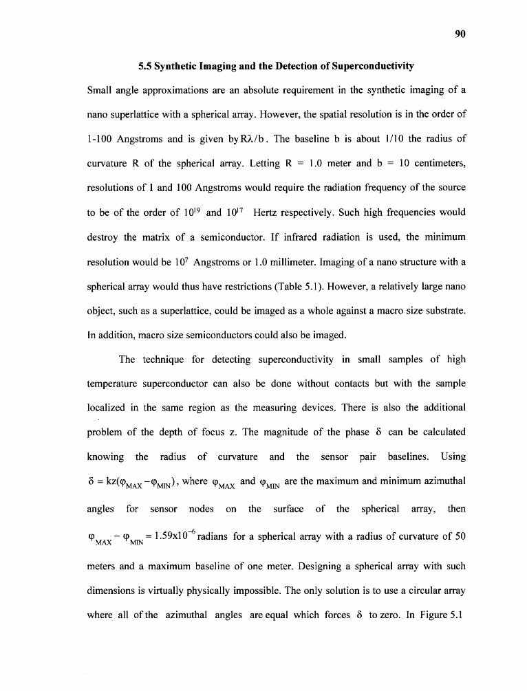
90
5.5 Synthetic Imaging and the Detection of Superconductivity
Small angle approximations are an absolute requirement in the synthetic imaging of a
nano superlattice with a spherical array. However, the spatial resolution is in the order of
1-100 Angstroms and is given byRλ/b . The baseline b is about 1/10 the radius of
curvature R of the spherical array. Letting R = 1.0 meter and b = 10 centimeters,
resolutions of 1 and 100 Angstroms would require the radiation frequency of the source
to be of the order of 1019 and 1017 Hertz respectively. Such high frequencies would
destroy the matrix of a semiconductor. If infrared radiation is used, the minimum
resolution would be 10 7 Angstroms or 1.0 millimeter. Imaging of a nano structure with a
spherical array would thus have restrictions (Table 5.1). However, a relatively large nano
object, such as a superlattice, could be imaged as a whole against a macro size substrate.
In addition, macro size semiconductors could also be imaged.
The technique for detecting superconductivity in small samples of high
temperature superconductor can also be done without contacts but with the sample
localized in the same region as the measuring devices. There is also the additional
problem of the depth of focus z. The magnitude of the phase δ can be calculated
knowing the radius of curvature and the sensor pair baselines. Using
δ = kz(φΜλχ - ΦΜ ) , where ΦΜΑΧ and ΦΜ ΙΝ are the maximum and minimum azimuthal
angles for sensor nodes on the surface of the spherical array, then
φ - φMDX
= 1.59Α10 -6 radians for a spherical array with a radius of curvature of 50ΜΙΝ
meters and a maximum baseline of one meter. Designing a spherical array with such
dimensions is virtually physically impossible. The only solution is to use a circular array
where all of the azimuthal angles are equal which forces δ to zero. In Figure 5.1

91
the dimensions of the sample and window are 30 and 15 mm, respectively. According to
Table 5.1, the frequency of the radiation source can be at least 3.0x10 12 Hertz and with
no problems with either resolution of depth of focus.
0Table 5.1 Wavelength, Frequency and SR (R 0 = 1.0 meter, b = 10 cm, SR, λ are in A )
The sample could be placed within the inductor of a Colpitts oscillator. The
precise quantity of feedback is finely adjusted to maintain oscillation at set amplitude.
The presence of superconductivity is detected through a small but sudden change in
frequency and an increase in the gain required to maintain oscillations. Upon cooling
through the transition temperature of ΤΤ , a cuprate superconducting sample in an
induction coil will experience a sharp reduction in Q (gain) corresponding to a loss of
energy to the sample. This loss will reach a maximum just below Ρ. Since no electrical
contacts are necessary, the technique is suitable for samples in either bulk or powder
form. However, the technique is not remote so the presence of cryogenic temperatures
may affect the measuring apparatus.
To detect superconductivity remotely using a spherical array, a plausible method
would be to follow a scheme based reflectivity profiles and parameters in terms of R
(Figure 5.17). The source of radiation could beam at the material in a normal
incidence and a spherical array could be used to determine the existence of energy

92
absorption in a normal state semiconductor (Figure 5.18). R can be determined
knowing the reconstructed intensity of radiation incident upon the surface of the
semiconductor. R can also be determined theoretically from the electromagnetic
boundary conditions on the surface of the conducting semiconductor. Ambient
background interference may cause a problem in reconstructing the intensity profiles of
the semiconductor.
Figure 5.16 Circular array imaging sample in a cryostat. Window-to-window distance fortransmission geometry: 120 mm, windows diameter 15 mm, sample space: 30 mm.
However, an intensity vs. frequency profile could still be used to determine the
onset of superconductivity. The "distorted" profiles resulting from interference are
repeated with the same range of frequency scans and any noticeable disruption in the
profile can be used to deduce the presence of superconductivity as the temperature of the
superconductor is lowered towards T^ .

Figure 5.17 Scheme for determining superconductivity in a superlattice using a circulararray.
In a more analytically way, one can determine the onset of SC my defining certain
variables and conditions (see Appendix D and Figure 5.17). If the imaginary part of a k
vector (k_) of an EΜ wave in a material is negligible, if 1 » ‚Ισμ oc2 /(ωC2), then there
is no energy absorption in the semiconductor; else if 1 « ‚/σμ oc2 /(ωC2) , then energy is
being absorbed.
An EΜ wave entering a semiconductor in a SC state, the B field drats off

94
exponentially [47] and magnetic fields are confined to an area within the London
penetration depth λs . The wave must travel a distance λ L before the fields drat off
by a factor of e 1 . The magnetic fields are confined to a region not far from the
surface of the material whose spatial extent is λ ι (Figure 5.18). For an EΜ wave
entering a semiconductor in a normal state, the imaginary k vector may be such that the
electric and magnetic fields of a wave dissipates by a factor of e - ' at a distance into a
conductive medium that may be less than or greater than to λ ι . If k_ < λL -1 , then the
wave must travel a distance greater than λL before the field drops off by a factor of e 1 .
As the medium becomes SC, k_ and ‚/σμ oc2 /(ωC2) must both increase so that
k_λL = 1 when the material is SC. If k> λ ι -1 , then the wave must travel a distance less
than λL before the field drops off by a factor of e- '. As the medium becomes SC, k_ and
‚Ισμoc2 /(ωC2) must both decrease so that k_λL = 1 when the material is Sc.
Reflectivity profiles of semiconductors can be used to estimate Cooper pair
binding energies. Researchers have made a high temperature superconductor of bismuth,
strontium, calcium, catper and oxygen. The superconductor has a Tc of 88 K. By
analyzing the light reflected from the material above and below 88 K, researchers can tell
which frequencies of light it absorbed. The energies of these photons are related to the
binding energy of the electron pairs in the superconductor [40].

95
Figure 5.18 EΜ wave entering a semiconductor in superconducting state.
For a superconductor, if the incident frequency is below Δ/h, where A is the
energu gap, the conductivity will be zero and the reflectivity will be unity. The
theoretical reflectivity profiles for LSCO (La 2_χSr ΧCυΟ4 ) are shown in Figures 5.19
[48]. The reflectivity is plotted against ω/Δ, where γ is the level broadening. The level
broadening is a measure of the degree of electronic scattering. At T=0 K, there is a
cutoff frequency at ω/ Δ = 0.7 , below which the reflectivity is unity. The material below
that point has zero conductivity. When γ = 0, there will no electron scattering, creating a
pure Bloch electron state. As T increases, the reflectivity profiles show marked
differences. Other materials will show differences in the reflectivity profiles as T is
varied from below T to above Ρ. In general, as a semiconductor is cooled towards the
critical temperature, the reflectivity profile changes. The reflectivity profiles, generated
by sensor arrays, can thus easily be used to determine the onset of SC at T is lowered
towards the critical temperature.

Figure 5.19 Reflectivity of LSCO as a function of the frequency for fixed impurityscattering rate with different temperatures (from Figure lc of Reference 48).
96

CHAPTER 6
CONCLUSIONS
This thesis has evaluated conditions for semiconductor superlattice structures for which
high — ΤΤ superconductivity is feasible via both theoretical arguments and results of
computer simulations. Analysis of computer simulations, with numerous superlattice
designs and dating concentrations, seem to support the theoretical argument that Fermi
energies and interplanar Coulomb interaction are factors that determine the formation of
the quantum wells with electron and hole carrier layers. The Coulomb interactions
between layers in a superlattice are a strong factor affecting the feasibility of designing a
HTS superlattice that satisfies all the criteria of the Harshman formulation. None of the
computer simulations in this study indicated that a superlattice structure that satisfies all
the criteria of the Harshman model was possible.
The computer simulations emulated the electronic structure of
high - Τc superconductor superlattices with β = 1. Results are based on a maximum
built-in electrostatic field of 500 kV cm 1 and a sheet resistance of 10 4 Ohms, which
dictates a minimum superlattice period of d = 80 nm and a corresponding sheet carrier
density of electrons and holes is N = 1.56 x 10 10 cm 2 . Based on a strong-coupling
electronic model of superconductivity, a superconductor with a transition temperature of
2 K will result from such an electron-hole superlattice.
Synthetic imaging of macro objects in the near field is only possible with circular
arrays if small angle approximations exist. Circular arrays can be used to detect the
existence of superconductivity in semiconductor material.
97

APPENDIX A
DERIVATION OF LOGARITHMIC DERIVATIVE OFTHE CRITICAL TEMPERATURE
98
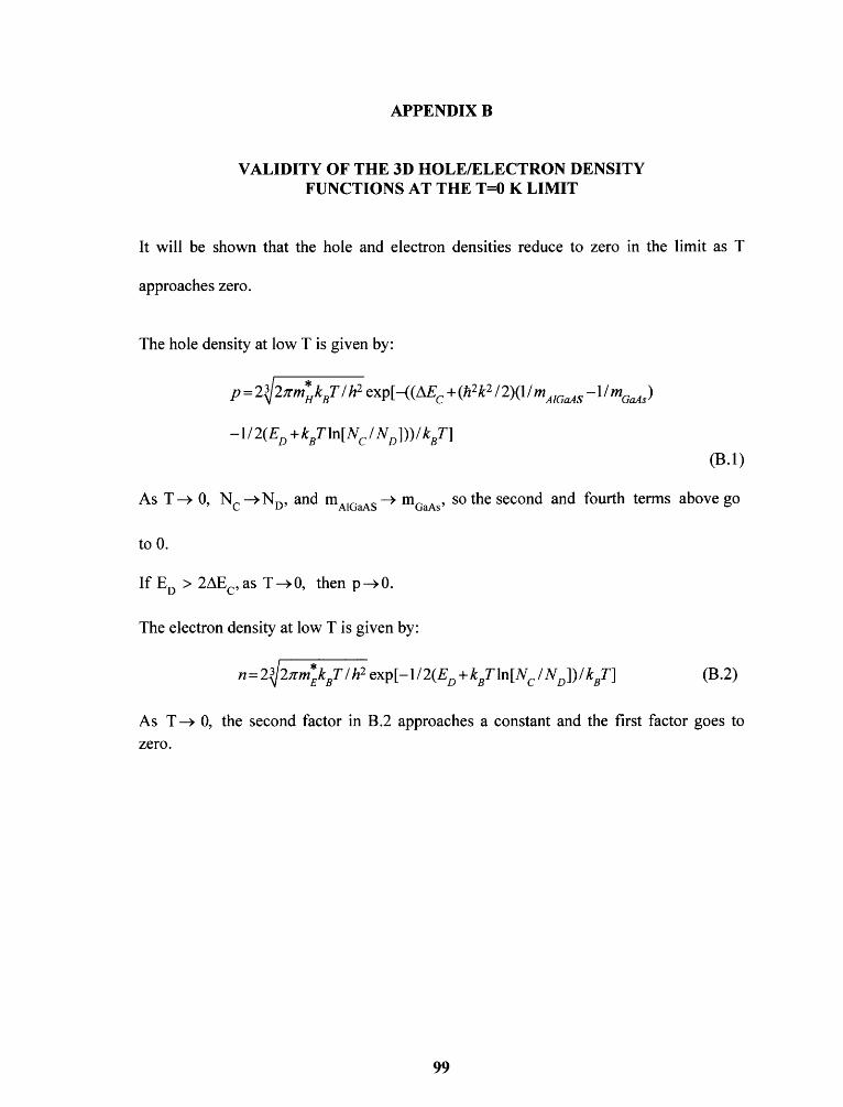
APPENDIX B
VALIDITY OF THE 3D HOLE/ELECTRON DENSITYFUNCTIONS AT THE T=0 K LIMIT
It will be shown that the hole and electron densities reduce to zero in the limit as T
approaches zero.
The hole density at low T is given by:
99

APPENDIX C
THE 2-D INVERSE FOURIER TRANSFORM (IFT) OF THE PRODUCT OFTWO DISPLACEMENT VECTORS AND THE CORRELATION FUNCTION
To prove the theorem that the 2-D Inverse Fourier Transform (IFT) of the product of
2r;r^ and the correlation c(i,j) between 2 sensor points located at r i,rj yields the intensity
distribution on the surface of an illuminated object.
Let ri ,rj be the distances from a source point 1 to sensors i , j respectively and E(x,y) is
the amplitude of the wave field at the source point and k is the wave number. Κ 1 and k2
are dummy variables that will be used in integrations. The sensors are in a plane that is
parallel to the plane containing the source point as shown in Figure C.1 since one can
assume small angle approximations. Since E(x,y) is real, IE(x,y)I 2 can be expressed as

101

a partial reconstruction of the intensity distribution. To fully reconstruct the image of an
object, a large number of pairs of sensor nodes would be needed.
102
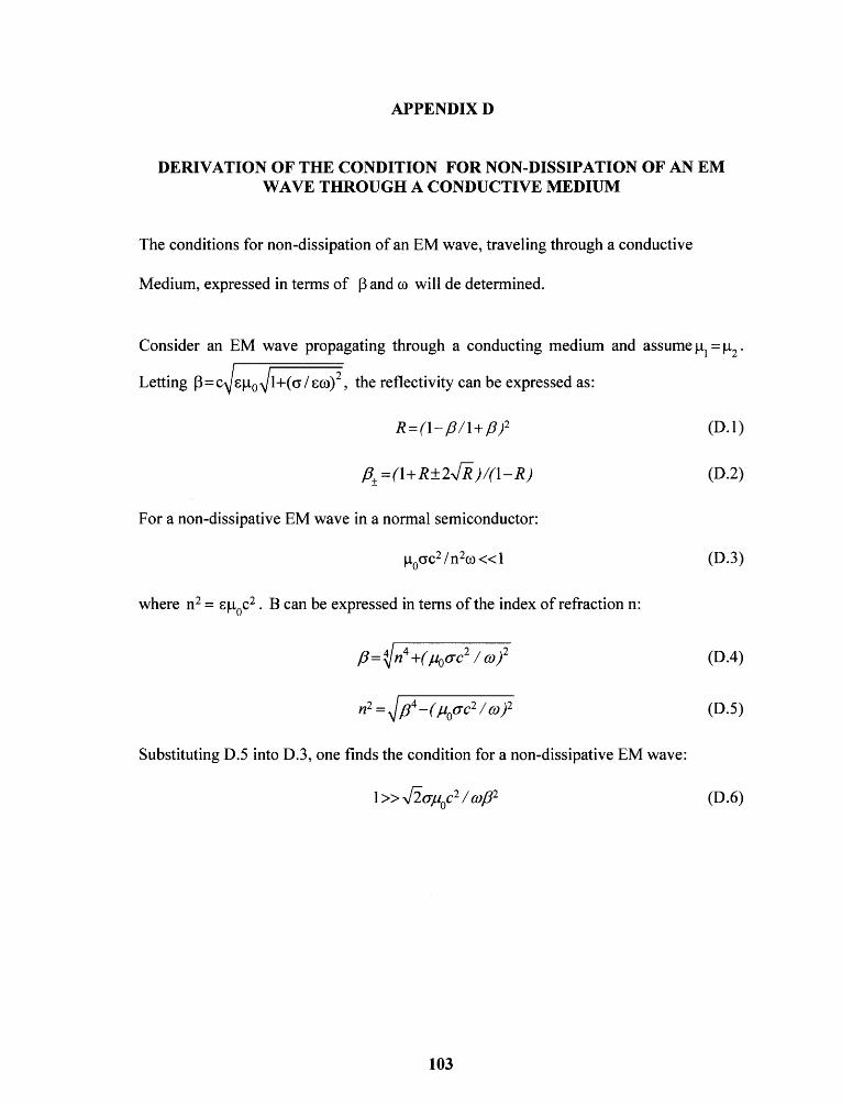
APPENDIX D
DERIVATION OF THE CONDITION FOR NON-DISSIPATION OF AN EMWAVE THROUGH A CONDUCTIVE MEDIUM
The conditions for nonoissipation of an EM wave, traveling through a conductive
Medium, expressed in terms of β and w will de determined.
Consider an EM wave ρropaαatinα through a conductin medium and assume Li, = μ, .
103

REFERENCES
1. Harshman, D. & Mills, A. (1992). Concerning the nature of high-Tc
superconductivity: Survey of experimental properties and implications forinterlayer coupling. Physical Review, Volume B45, No. 18, 10701.
2. Tan, H., Snider G., Chang, G. D., & Hu, E. (1990). A self-consistent solution ofSchώdinger-Poisson equations using a nonuniform mesh. Journal of AppliedPhysics, Volume 68, Number 8, 4071.
3. Homes, C., Dordevic, S. V., Strongin, M., Bonn, D. A., Liang, R., Hardy, W. N.,Komiya, S., Ando, Y., Yu, G., Kaneko, N., Chao, X., Greven, M., Basovand, D.N., & Timusk, T. (2004). A universal scaling relation in high-temperaturesuperconductors. Nature 430, 539.
4. Hirsch, J. E. (1997). Correlations between normal-state praterties andsuperconductivity. Physical Review, Volume B55, Number 14, 9007-9024.
5. Flukiger, R. (1992). A snapshot view of high temperature superconductivity 2002.Concise Encyclopedia of Magnetic and Superconducting Material, PergamonPress, Inc., 1.
6. Fisher, O. & Maple, M. B. (1982). Superconductivity in Ternary Compounds.Springer-Verlag, Berlin, 1.
7. Etourneau, J. (1992). Solid State Chemistry: Compounds. Clarendon Press, Oxford, 60.
8. Vonsovsky, S. V., Izyunov, Y. A., & Kurmaev, E. Z. (2002). A snapshot view ofhigh temperature superconductivity 2002. Springer Series in Solid State Sciences, Springer-Verlag, Berlin, 259.
9. Bud'ko, S. L., Lapertot, G., Petrovic, C., Cunningham, C. E., Anderson, N., &Canfield, P. (2001). Upper critical field and irreversibility line insuperconducting MgB2 . Solid State Communication, Volume 118, Number 497,
1.
10. Mohanty, P., Wei, J. Y. T., Ananth, V., Morales, P., & Skocpol, W. (2004).Nanoscale high-temperature superconductivity. Physics C 408-410, 666-669.
11. D. R. Harshman, unpublished paper.
12. D. R. Harshman, private communication.
104

13. Shore, H. B., Caremba, E., & Sander, L. (1978). Density-functional theory ofWigner crystallization. Physical Review, Volume B 18, Number 12, 6506-6509
14. Valenzuela, B., Fratini, S., & Baeriswyl, D. (2003). Charge and spin order in one-dimensional electron systems with long-range Coulomb interactions. Physical Review, Volume B68, Number 045112, 1-11
15. Keimer, B. (2005). Superconductors: the mystery goes on. Physics World, AprilIssue, 48.
16. Snider, G. (2005). 1D Poisson/Schrδdinger User's Manual.http://www.nd.edu/-gsnider, University of Notre Dame, Notre Dame, Indiana.
17. Ram-Mohan, L. (2002). Finite Element and Boundary Element Applications inQuantum Mechanics. Oxford University Press, 241-256.
18. Bardeen, J., Cooper, L. N., & Schrieffer, J. R. (1957). Theory ofSuperconductivity. Physical Review, Volume 108, Number 5, 1175.
19. Bednorz, J. G. & Mueller, K. A. (1986). Possible high-Tc superconductivity in the
Ba-La-Cu-O system. Ζ Physics B, Condensed Matter, Volume 64, 189-193.
20. Long, M. W. (1990). Low spin correlations between copper spins in oxygen holesuperconductors. Journal of Physics: Condensed. Matter, Volume 2, Number 16,3823-3839.
21. Hirsch, J. (2002). Why holes are not like electrons. Physical Review, Volume B65,Number 18, 4502.
22. D. R. Harshman, private communication.
23. Hirsch, J. (1989). Hole conductors and superconductors. Materials ResearchSociety Symposium Proceedings, Volume 156, 349.
24. Kittel, C. (2004). Introduction to solid state physics. Eight Edition, John Wiley & Sons, Inc., 662.
25. Lynn, J. W. (1990). High temperature superconductivity. Springer-Verlag, NewYork, 16.
26. Lanzara, A., Bogdanov, P. V., Chou, X. J., Kellar, S. A., Feng, D. L., Lu, E.D.,Yoshida, T., Eisaki, H., Fujimori, A., Kishio, K., Shimoyama, J., Noda, T.,Uchida, S., Hussain, Z., & Shen, Z.X. (2001). Evidence for ubiquitous strongelectron-phonon coupling in high temperature superconductors. Nature 41, 510-514.
105

27. Carlson, E. W., Emery, V. J., Kivelson, S. A., & Orgad, D. (2002). Concepts inHigh Temperature Superconductivity. Retrieved June 6 2006 from the WorldWide Web: http://arxιv.org/PS_cache/cοnd-mat/pdf/0206/0206217.pdf, 10.
28. Balandin, A. (2002). Thermal Properties of Semiconductor Low-DimensionalStructures. Physics of Low-Dimensional Structures, Volume 1/2, Number 1, 1-43.
29. Tien, C. L & Chen, G. (1994). Challenges in Microscale Conductive andRadiative Heat Transfer. ASME Journal of Heat Transfer, Volume 116, 799.
30. Xiao, Y., Thorpe, M. F., & Parkinson, J. B. (1999). Twooimensional discreteCoulomb alloy. Physical Review, Volume B59, Number 1, 277-285.
31. Wetzel, C., Efros, A., Moll, A., & Meyer, B. (1992). Dependence on quantumconfinement of the in-plane effective mass in Gaο 47In0 53As/InΡquantum wells.Physical Review, Volume B45, Number 24, 45.
32. Majumda, A., Rokhinson, L. P., Tsui, D. C., Pfeiffer, L. N., & West, K. W. (2002).Effective mass enhancement of twooimensional electrons in a oneoimensionalsuperlattice potential. Applied Physics Letters Volume 76, Number 24, 3600.
33. Ebihara, T., Bauer, E. D., Cornelius, A.L., Lawrence, J. M., Harrison, N.,Thompson, J. D., Sarrao, J. L., Hundley, M. F., & Uji, S. (2003). Dependence ofthe Effective Masses in YbA1 3 on Magnetic Field and Disorder. Physical Review
Letters, Volume 90, Number 16, 6404.
34. Davies, J. H. (1998). The Physics of Low-Dimensional Semiconductors.Cambridge University Press, 145.
35. Yariv, A. (1982). An Introduction to Theory and Applications of QuantumMechanics. John Wiley & Sons, 247-249.
36. Cole, B. E., Chamberlain, J. M., Henini, M., Cheng, T., Batty, W., & Wittlin, A.(1997). Cyclotron Resonance in Ultra-low Hole Density, Narrow, p-typeGaAs/(A1,Ga)As QuantumWells. Physical Review, Volume B55, 2503-2511.
37. Walsh, K.P., Fiory, A. T., Ravindra, N. M., Harshman, D. R. & Dow, J. D. (2006).Electron-Hole superlattices in GaAs/A1 χGa1_χAs multiple quantum wells.Philosophical Magazine, Volume 86, Number 23, 3593.
38. Huxley, A., Sheikin, I., Ressouche, E., Kernavanois, N., Braithwaite, D.,Calemczuk, R., & Flouquet, J. (2001). UGe2: A ferromagnetic spin-triplesuperconductor. Physical Review, Volume B63, Number 144519, 1.
39 Millis, A. J. (2000). Advances in the Physics of High-TemperatureSuperconductivity. Science, Volume 288, Number 5465, 468.
106

40. Pennicott, Κ. (2002). Superconductivity clue comes out of the blue. Retrieved 6June 2006 from the World Wide Web: http://physicsweb.org/articles/news/6/3/17.
41. Eck, E. J. (2005). Confirmation: Planar Weight Disparity Improves Τ. Retrieved 6June 2006 from the World Wide Web:http://www. superconductors.org/3 2121212.htm.
42. Timusk, Τ. (2005). High-temperature uncertainty. Physics World, Volume 18, Number 7, 35.
43. Naidu, P. S. (2000). Sensor Array Signal Processing. CRC Press, prologue.
44. Walsh, K.P., Schulkin, B., Gary, D., Federici, J. F., Barat, R. & Cimdars, D. (2004).Terahertz near field interferometric and synthetic aperture imaging. ProceedingsSPIE, Volume 5411, 1-9.
45. Griffiths, D. J. (1999). Introduction to Electrodynamics. Prentice Hall, 309.
46. Christy, R. W., Milford, F. J., & Reitz, J. R. (1992). Foundations ofElectromagnetic Theory. Addison-Wesley, 405.
47. Ashcroft, N. W. & Mermin, N. D (1976). Solid State Physics. Saunder College,739.
48. Sarma, S. D. & Hwang, E. H. (2002). On the c-axis optical reflectivity of layeredcuprate. Physical Review Letters, Volume 80, Number 21, 4753-4756.
107