Handbook of Semiconductor Wafer Cleaning Technology
42
Science, Technology, and Applications Edited by Werner Kern Werner Kern Associates East Windsor, New Jersey NOYES PUBLICATIONS Park Ridge, New Jersey, U.S.A.
-
Upload
khangminh22 -
Category
Documents
-
view
1 -
download
0
Transcript of Handbook of Semiconductor Wafer Cleaning Technology
Science, Technology, and Applications
Edited by
Werner Kern
Werner Kern Associates East Windsor, New Jersey
NOYES PUBLICATIONS Park Ridge, New Jersey, U.S.A.

6
JVHN H. VIG, Ph.D.
! Chief, Frequency Control & Timing Branch
ARMY RESEARCH LABORATORY Electronics & Power Sources Directorate
: Office: (908) 544-4275 , FAX: (908) 544-4323 I DSN: 995-
Attn: AMSRL-EP-ME Ft. Monmouth, NJ 07703-5601
Ultraviolet-Ozone Cleaning Of Semiconductor Surfaces
John R. Vig
1.0 INTRODUCTION
The capability of ultraviolet (UV) light to decompose organic mol- ecules has been known for a long time, but it is only since the mid-l 970s that UV cleaning of surfaces has been explored (1)-(6). Since 1976, use of the UV/ozone cleaning method has grown steadily. UWozone cleaners are now ava i la ble commercia I I y from severa I manufacturers.
2.0 HISTORY OF UV/OZONE CLEANING
That ultraviolet light causes chemical changes has been generally known for a long time. Commonly known manifestations are the fading of fabric colors and changes in human skin pigmentation (i-e., sun tanning) upon exposure to sunlight. The chemical changes produced by short wavelength UV light inside the cells of living organisms can damage or destroy the cells. An important use of UV lamps has been as "germicidal" lamps, e.g., for destroying microorganisms in hospital operating rooms and in the air ducts of air conditioning systems (7).
In 1972, Bolon and Kunz (1) reported that UV light had the capability to depolymerize a variety of photoresist polymers. The polymer films were enclosed in a quartz tube that was evacuated and then backfilled with oxygen. The sampleswere irradiated with UV light from a medium-pressure mercury lamp that generated ozone. The polymer films of several thousand angstroms thickness were successfully depolymerized in less than one hour. The major products of depolymerization were found to be water and
233
1 i \
234 Handbook of Semiconductor Wafer Cleaning Technology
carbon dioxide Subsequent to depolymerization, the substrates were examined by Auger electron spectroscopy (AES) and were found to be free of carbonaceous residues Only inorganic residues. such as tin and chlorine, were found When a Pyrex filter was placed between the UV light and the films, or when a nitrogen atmosphere was used instead of oxygen, the depolymerization was hindered Thus, Bolon and Kunz recognized that oxygen and wavelengths shorter than 300 nm played a role in the depolym- erization
In 1974, Sowell et al. (2) described UV cleaning of adsorbed hydrocar- bons from glass and gold surfaces, in air and in a vacuum system A clean glass surface was obtained after- fifteen hours of exposure to the UV radiation in air torr of oxygen, clean gold surfaces were produced after about two hours of UV exposure During cleaning, the partial pressure of 0, decreased, while that of CO, and H,O increased. The UV a!co desorbed gases from the vacuum r,hamberwa!ls. In air, gold surfaces which had been contaminated by adsorbed hydrocar- bons could be cleaned by “several hours of exposure to the UV radiation.” Sowell et al. also noted that storing clean surfaces under UV radiation ma i nt ained the su rface cleanliness indefinitely .
During the period 1974 - 1976, Vig et al (3)-(5) described a series of experiments aimed at determining the optimum conditions for producing clean surfaces by UV irradiation The variables of cleaning by UV light were defined, and it was shown that, under the proper conditions, UWozone cleaning has the capability of producing clean surfaces in less than one minute
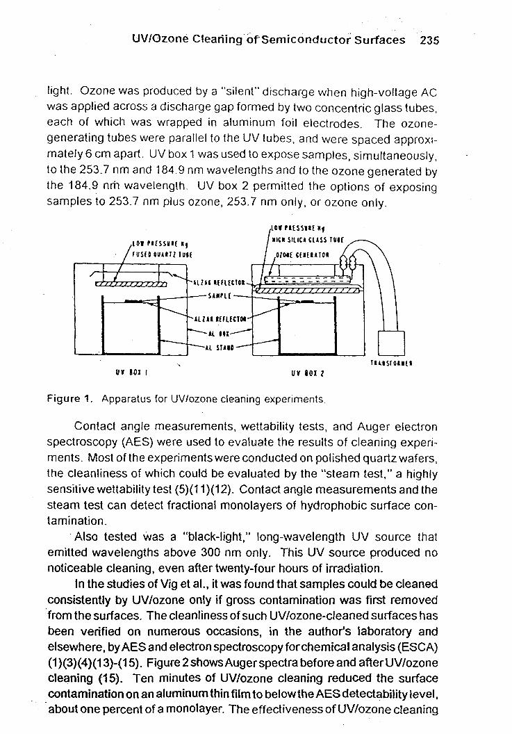
To study the variables of the UV cleaning procedure, Vig and LeBus (5) constructed the two UV cleaning boxes shown in Fig. 1. Both were made of aluminum and both contained low-pressure mercury discharge lamps and an aluminum stand with Alzak (8) reflectors. The two lamps produced nearly equal intensities of short-wavelength UV light, about 1.6 mW/cm2 for a sample 1 cm from the tube. Both boxes contained room air (in a clean room) throughout these experiments. The boxes were completely enclosed to reduce recontaminations by air circulation.
The tube of the UV lamp (8) in box 1 consisted of 91 cm of “hairpin- bent” fused quartz tubing. The fused quartz transmits both the 253.7 nm and the 184.9 nm wavelengths. The lamp emitted about 0.1 mW/cm2 of 184.8 nm radiation measured at 1 cm from the tube. The lamp in box 2 had two straight and parallel 46 cm long high-silica glass tubes made of Coming UV Glass NO. 9823, which transmits at 253.7 nm but not at 184.9 nm. Since
generator (9) was built into box 2. This ozone generator did not emit UV
In a vacuum system at
I
this lamp generated no measurable ozone, a separate Siemens-type ozone i
1
lig
ea ge mi to the sals
Wc‘
Fig
SPt
me the se I
ste tan
em not
cor fro1 be( els
cl e
a bl
(1)
COI
UV/Ozone Cleariing‘of Semiconductor Surfaces 235
light. Ozone was produced by a “silent” discharge when high-voltage AC was applied across a discharge gap formed by two concentric glass tubes, each of which was wrapped in aluminum foil electrodes. The ozone- generating tubes were parallel to the UV tubes, and were spaced approxi- mately 6 cm apart. UV box 1 was used to expose samples, simultaneously, to the 253.7 nm and 184.9 nm wavelengths and to the ozone generated by the 184.9 nm wavelength. UV box 2 permitted the options of exposing samples to 253.7 nm plus ozone, 253.7 nm only, or ozone only.
Yltl SILICA C L A S S TU8
U Y I O X I u v BOX 2
Figure 1. Apparatus for UV/ozone deaning experiments
Contact angle measurements, wettability tests, and Auger electron spectroscopy (AES) were used to evaluate the results of cleaning experi- ments. Most of the experiments were conducted on polished quartz wafers, the cleanliness of which could be evaluated by the “steam test,” a highly sensitive wettability test (5)(11)(12). Contact angle measurements and the steam test can detect fractional monolayers of hydrophobic surface con- tamination.
Also tested was a “black-light,” long-wavelength UV source that emitted wavelengths above 300 nm only. This UV source produced no noticeable cleaning, even after twenty-four hours of irradiation.
In the studies of Vig et al., it was found that samples could be cleaned consistently by UV/ozone only if gross contamination was first removed from the surfaces. The cleanliness of such UV/ozone-cleaned surfaces has been verified on numerous occasions, in the author‘s laboratory and elsewhere, by AES and electron spectroscopy for chemical analysis (ESCA) (1)(3)(4)(13)-(I 5). Figure 2 shows Auger spectra before and after UWozone cleaning (15). Ten minutes of UV/ozone cleaning reduced the surface contamination on an aluminum thin film to below the AESdetectability level, about one percent of a monolayer. The effectiveness of UWozone cleaning

. .* 236 . Handbook of Semiconductor Wafer Cleaning Technology
has also been confirmed by ton scattering spectroscopy/secondary ion mass spectroscopy (ESS/SIMS) (16).
I
0 200 400 600 800 1000
Electron energy (eV)
Figure 2. Auger spectra of evaporated aluminum film on silicon substrate: (a) before UV/ozone cleaning; (b) after UV/ozone cleaning.
P '
I .

W/Ozone Cleaning of Semiconductor Surfaces 237 I a-
253.7 nm, no 0, l h 253.7 nm + 0, 253.7 nm + 184.9 nm + 0,
SIC! 2 20 s
A number of wafers of AT-cut quartz crystal were precleaned and exposed to the UV light In box 1 until clean surfaces were obtained. Each of the wafers was then thoroughly contaminated with human skin oil, which has been a difficult contaminant to remove. (The skin oil was applied by rubbing a clean wafer on the forehead of one of the researchers.) The wafers were precleaned again, groups of wafers were exposed to each of the four UV/ozone combinations mentioned earlier, and the time needed to attain a clean surface, as indicated by the steam test, was measured. In each UV box, the samples were placed within 5 mm of the UV source (where the temperature was about 7OOC).
The wafers exposed to 253.7 nm + 184.9 nm + ozone in UV box 1 became clean in 20 seconds The samples exposed to 253 7 rim + ozone i n UV box 2 reached the clean condition in 90 seconds. Samples exposed to 253.7 nm without ozone and to ozone without UV light were cleaned within one hour and ten hours, respectively. The results are summarized in Table 1.
I
Table 1. Exposure Types vs. Cleaning Times i
cleaning method is now used in a variety of applications, in electronics, optics, and other fields.
3.0 VARfABLES OF UVIOZONE CLEANING
Exposure type Time to reach clean condition
3.1 Wavelengths Emitted by the UV Sources
Since only the light that is absorbed can be effective in producing photochemical changes, the wavelengths emitted by the UV sources are
238 Handbook of Semiconductor Wafer Cleaning Technology
important variables. The low-pressure mercury discharge tubes generate two wavelengths of interest: 184.9 nm and 253.7 nm. Whether or not these wavelengths are emitted depends upon the lamp envelopes. The emis- sions through the three main types of envelopes are summarized in Table 2. Pure quartz IS highly transparent to both wavelengths.
Table 2. Principal Wavelengths of Low-Pressure Hg Discharge Lamps
Lamp envelope* Wavelength (nm) Fused quartz High-silica glass Glass
184.9 T 0 0
253.7 T T 0
300.0 T T T
7 = t ransparent , 0 = o p a q u e
The 184.9 nm wavelength is important because it is absorbed by oxygen, thus leading to the generation of ozone (1 7), and it IS also absorbed by many organic molecules. The 253.7 nm radiation is not absorbed by oxygen, therefore, it does not contribute to ozone generation, but IS
absorbed by most organic molecules (18)(19) and by ozone (17). The absorption by ozone is principally responsible for the destruction of ozone in the UV box. Therefore, when both wavelengths are present, ozone is continually being formed and destroyed. An intermediate product, both of the formation and of the destruction processes, is atomic oxygen, which is a verystrong oxidizing agent. The absorption of either or both wavelengths by the organic and other contaminant molecules results in the dissociation or excitation of those molecules. The reaction of the atomic oxygen with excited or dissociated contaminant molecules is believed to be responsible for the cleaning action of UV/ozone, as is discussed below.
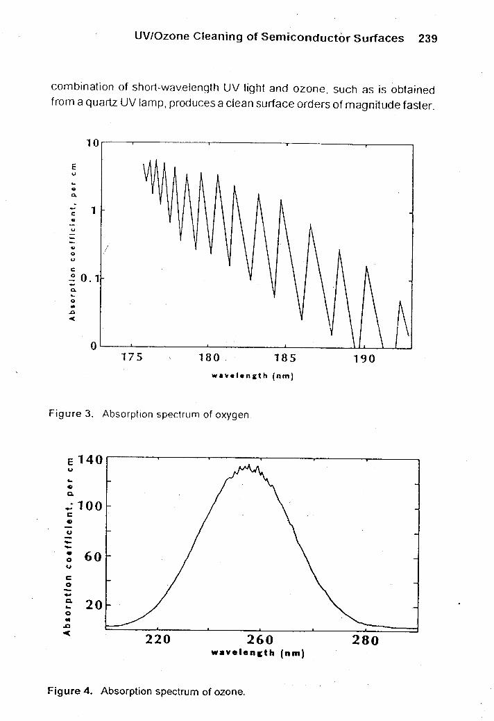
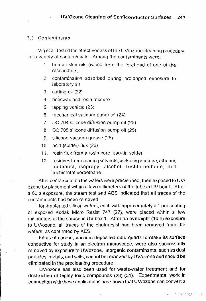
The absorption spectrum of oxygen isshown in Fig. 3 and that of ozone in Fig. 4. The effects of the principal wavelengths generated by low- pressure mercury discharge lamps are summarized in Table 3.
In the studies of Vig et al., wafers exposed to 253.7 nm + 184.9 nm + Ozone became clean much faster than the samples exposed to 253.7 nm + Ozone only, or to 253.7 nm without ozone, or to ozone without UV light, as is summarized in Table 1. Therefore, although both UVlight without ozone and ozone without UV light can produce a slow cleaning effect in air, the
I
UV/Ozone Cleaning of Semiconductor Surfaces 239
combination of short-wavelength UV light and ozone, s u c h as is obtained from a quartz UV lamp, produces a clean surface orders of magnitude faster.
i a
1
0 175 180 185 190
w a v o l o n g t h (nm)
Figure 3. Absorption spectrum of oxygen
Y
C Q
0 - - L c 0 0 V
E 0 - - L n 0 a
*
E 140 u L
4 n - 100
6 0
2 0
220 2 6 0 2 8 0 wave length (nm)
Figure 4. Absorption spectrum of ozone.

240 Handbook of Semiconductor Wafer Cleaning Technology
Table 3. Effects of the Principal Wavelengths Generated by Low- Pressure Hg Discharge Lamps I
Wavelength (nm) Effects I I
184.9 Absorbed by 0, and organic molecules Creates atomic oxygen and ozone Breaks contaminant molecule bonds
253.7 Absorbed by organic molecules and 0,; I riot absorbed by 0,
Destroys ozone Breaks contaminant molecule bonds
3.2 Distance Between the Sample and UV Source i
Ar?o!her variable that can greatly affer,? the c!eaning rate is !he distance between the sample and the UV source. In Vig et al.'s experiment, !he UV
i 1 i 1 lamps were essentially plane sources. Therefore, one may conclude that the
intensity of UV light reaching a sample would be nearly independent of distance. However. this is not so when ozone is present, because ozone has a broad absorption band ( I 7)(20)(21) centered at about 260 nm, as is shown in Fig. 4. At 253.7 nm, the absorption coefficient is 130/cm.atm. The intensity 1 of the 253.7 nm radiation reaching a sample therefore decreases as
:
130pd I = lee-
where p is the average ozone pressure between the sample and the UV soiirce in atmospheres at OOC, and d is the distance to the sample in centimeters. When a quartz UV tube is used, both the ozone coricentration and t h e UV radiation intensity decrease with distance from the UV source.
Two sets of identically precleaned samples were placed in UV box 2. One set was placed within 5 mm of the UV tube, the other was placed at the bottom of the box about 8 cm from the tube. With the ozone generator off, there was less than a thirty-percent difference in the time it took for the two sets of samples to attain a minimal (approximately 4 O ) contact angle, about 60 min vs. 75 min. When the experiment was repeated with the ozone generator on, the samples near the tube became clean nearly ten times faster (about 90 s vs. 13 niin). Similarly, in UV box 1, samples placed within 5 mm of an ozone-producing UV tube were cleaned in 20 s vs. 20 - 30 min for samples placed near the bottom of the box at a distance of 13 cm. Therefore, to maximize the cleaning rate, the samples should be placed as close as practicable to the UV solme.
I
I
A ,
3.3
for;
0201
a 6C coni
of f
milli to L waff
con( rem' parti elim
dest coni
. * _.,
* .
!
I
1
I i
1 I
!
. UV/Ozone Weaning of Semiconductor Surfaces 241
3.3 Contaminants
Vig et al. tested the effectiveness of the UWozone cleaning procedure for a variety of contaminants. Among the contaminants were:
I .
2.
3.
4.
5.
6 .
7 .
8.
9.
10.
11.
12.
human skin oils (wiped from the forehead of one of the researchers)
contamination adsorbed during prolonged exposure to laboratory air
cutting oil (22)
beeswax and rosin mixture
lapping vehicle (23)
mechanical vacuum pump oil (24)
DC 704 silicone diffusion pump oil (25)
DC 705 silicone diffusion pump oil (25)
silicone vacuum grease (25)
acid (solder) flux (26) rosin flux from a rosin core lead-tin solder
residues from cleaning solvents, including acetone, ethanol. methanol, isopropyl alcohol, t richloroet han e, and trichlorotrifluoroethane.
After contamination the wafers were precleaned, then exposed to UVI ozone by placement within a few millimeters of the tube in UV box 1. After a 60 s exposure, the steam test and AES indicated that all traces of the contaminants had been removed.
ion-implanted silicon wafers, each with approximately a 1 pm coating of exposed Kodak Micro Resist 747 (27), were placed within a few millimeters of the source in UV box 1. After an overnight (1 0 h) exposure to UWozone, all traces of the photoresist had been removed from the wafers, as confirmed by AES.
Films of carbon, vacuum-deposited onto quartz to make its surface conductive for study in an electron microscope, were also successfully removed by exposure to UWozone. Inorganic contaminants, such as dust particles, metals, and salts, cannot be removed by UV/ozone and should be eliminated in the precleaning procedure.
UV/ozone has also been used for waste-water treatment and for destruction of highly toxic compounds (28)-(31). Experimental work in connection with these applications has shown that UV/ozone can convert a
. ,, - ..; . ..._ . . . .... . ~

242 Handbook of Semiconductor Wafer Cleaning Technology
wide variety of organic and some inorganic species to relatively harmless. mostly volatile productssuch as CC,, CO, H20, arid N, Cor-rlpouridswtiicti have been destroyed successfully in water by UV/ozone include ethanol, acetic acid, glycine, glycerol, palmitic acid, organic nitrogen, phosphorus and sulfur compounds, potassium cyanide, complexed Cd, Cu, Fe, and Ni cyanides; photographic wastes, medical wastes, secondary effluents, chlo- rinated organics and pesticides such as pentachlorophenol, dichloroben- zene, dichlohutane, chloroform, malathion, Baygon, Vapam, and DOT It has also been shown (32) that using the combination of UVand ozone is more effective than using either one alone in destroying microbial contaminants ( E coli and streptococcus faecalis) in water UVlozone has been used for the breakdown of PCBs (33) A combination of UV, ozone and hydrogen peroxide is used in a commercial water treatment method (34). The UV breaks the hydrogen peroxide into atomic oxygen and hydroxyl radicals The hydroxyls assist with the breakdown of contaminant molecules. Forexample, benzene can be converted into carbon dioxide and water with this method
Ozone, dissolved in fluorocarbon solvents, plus UV has been used in a chemical warfare agent decontamination system (35). The combined effect of ozone plus UVwas found to be superior to either UVor ozone alone
3.4 Precleaning
Contaminants, such as thick photoresist coatings and pure carbon films, can be removed with UV/ozone without any precleaning, but, in general, gross contamination cannot be removed without precleaning. For example, when a clean wafer of crystal quartz was coated thoroughly with human skin oils and placed in UV box 1 (Fig. 1) without any precleaning, even prolonged exposure to UV/ozone failed to produce a low-contact- angle surface, because human skin oils contain materials, such as inorganic salts, which cannot be removed by photosensitized oxidation.
The UV/ozone removed silicones from surfaces which had been precleaned, as described earlier, and also from surfaces which had simply been wiped with a cloth to leave a thin film. However, when the removal of a thick film was attempted, the UWozone removed most of the film upon prolonged exposure but it also left a hard, cracked residue on the surface, possibly because many chemicals respond to radiation in various ways, depending upon whether or not oxygen is present. For instance, in the presence of oxygen, many polymers degrade when irradiated; whereas, in the absence of oxygen (as would be the case for the bulk of a thick film) these same polymers crosslink. In the study of the radiation degradation of
I
L .
PolYn differ
must meta oxidi. of wt actio
3.5
varie meta Quar mate
two (
plate Sincc the s that 1 it wa met t oxid;
work occu
the f
bec: Aftei
so IC dead su r f i
expc Silvt et a1 silvc the :
UVlOzone Cleaning of Semiconductor Surfaces 243 ...
polymers in air, the “results obtained with thin films are often markedly different from those obtained using thick specimen ...” (36).
For the UV/ozone cleaning procedure to perform reliably, the surfaces must be precleaned: first, to remove contaminants such as particles, metals, and salts that cannot be changed into volatile products by the oxidizing action of UWozone; and, second, to remove thick films the bulk of which could be transformed into a UV-resistant film by the crosslinking action of the UV light that penetrates the surface.
3.5 Substrate
The UV/ozone cleaning process has been used with success on a variety of surfaces, including glass, quartz, mica, sapphire, ceramics, metals, silicon, gallium arsenide, and a conductive polyimide cement. Quartz and sapphire are especially easy to clean with UV/ozone since these materials are transparent to short-wavelength UV.
For example, when a pile of thin quartz crystal plates, approximately two centimeters deep, was cleaned by UWozone, both sides of all the plates, even those at the bottom of the pile, were cleaned by the process. Since sapphire is even more transparent, it, too, could probably be cleaned the same way. When flat quartz plates were placed on top of each other so that there could have been little or no ozone circulation between the plates, it was possible to clean both sides of the plates by the UV/ozone cleaning method. It is interesting to note that Ref. 37 shows that photocatalytic oxidation of hydrocarbons, without the presence of gaseous oxygen, can occur on some oxide surfaces. This suggests that UV cleaning may also work on some surfaces in ultrahigh vacuum
When white alumina ceramic substrates were cleaned by UWozone, the surfaces were cleaned properly. However, the sides facing the UV became yellow, probably due to the production of UV induced colorcenters. After a few minutes at high temperatures (>16OoC), the white colorreturned.
Metal surfaces could be cleaned by UV/ozone without any problems, so long as the UV exposure was limited to the time required to produce a clean surface. (This time should be approximately one minute or less for surfaces which have been properly precleaned.) However, prolonged exposure of oxide-forming metals to UV light can produce rapid corrosion. Silver samples, for example, blackened within one hour in UV box 1 of Vig, et ai. Experiments with sheets of Kovar, stainless steel (type 302), gold, silver, and copper showed that, upon extended UV irradiation, the Kovar, the stainless steel, and the gold appeared unchanged, whereas the silver
I
.. 244 Handbook of Semiconductor Wafer Cleaning Technology
and copper oxidized on both sides, but the oxide layers were darker on the sides facing away from the UV source. When electroless gold-plated nickel parts were stored under UWozone for several days, a powdery black coating gradually appeared on the parts. Apparently, nickel diffused to the surface through pinholes in the gold plating, and the oxidized nickel eventually covered the gold nearly completely. The corrosion was also observed in UV box 2, even when no ozone was being generated. The rates of corrosion increased substantially when a beaker ofwaterwas placed in the UV boxes to increase the humidity. Even Kovar showed signs of corrosion under such conditions.
The corrosion may possibly be explained as follows: as is known in the science of air-pollution control, in the presence of short wavelength UV light and impurities in the air, such as oxides of nitrogen and sulfur, combine with water vapor to form a corrosive mist of nitric and sulfuric acids. Therefore, the use of controlled atmospheres in the UV box may minimize the corrosion problem.
Since UV/ozone dissociates organic molecules, i t may be a useful means of cleaning some organic materjals, just as etching and electropo- lishing are sometimes useful for cleaning metals. The process has been used successfully to clean quartz resonators which have been bonded with silver-filled polyimide cement (38). Teflon (TFE) tape exposed to UWozone
the contact angles measured on clean quartz plates increased after a piece
I
1
!
in UV box 1 for ten days experienced a weight loss of 2.5 percent (39). Also,
of Teflon was placed next to the plates in a UV box (40). Similarly, Viton shavings taken from an O-ring experienced a weight loss of 3.7 percent after
I !
I 1
24 hours in UV box 1. At the end of the 24 hours, the Viton surfaces had become sticky. Semiconductor surfaces have been successfully UV/ ozone-cleaned without adversely affecting the functioning of the devices. For example, after a 4 K static RAM silicon integrated circuit was exposed to UV/ozone for 120 min in a commercial UV/ozone cleaner, the device continued to function without any change in performance. This IC had been made using n-channel silicon gate technology, with 1 to 1.5 pm junction depths (41).
3.6 Rate Enhancement Techniques
UV/ozone cleaning “rate enhancement” techniques have been inves- tigated by Zafonte and Chiu (42). Experiments on gas phase enhancement techniques included a comparison of the cleaning rates in dry air, dry

FILTER
O - 7
, OZONE CENEAAlOR NI
PURGE .
oxygen, rnoist air, and molst oxygen. The moist air and moist oxygen consisted of gases that had been bubbled through water Oxygen that had been bubbled through hydrogen peroxide was also tried. Experiments on liquid enhancement techniques consisted of a drop-wise addition either of distilled water or of hydrogen peroxide solutions of various concentrations to the sample surfaces. Most of the sample surfaces consisted of various types of photoresist on silicon wafers.
The gas-phase "enhancement" techniques resulted in negligible to slight increases in the rates of photoresist removal (3 - 20 a /min without e r i h a i m " t vs. 3 - 30 h i i r n with enhancement). The water and hydrogen peroxide liquid-phase enhancement techniques both resulted in significant rate enhancements (1 00 - 200 A /min) for resists that were not exposed to ion implantation. The heavily "ion implanted" resists ( lot5 to 1Ol6 atoms/ cm2) were not significantly affected by UV/ozone, whether "enhanced" or not.
Photoresist removal rates of 800to 900r$/min for positive photoresists and 1500 to 1600 a/min for negative photoresists (43) were reported by one manufacturer of UWozone cleaning equipment (43). The fast removal rate was achieved at 3OOOC by using a 253.7 nm source of UV, a silent discharge ozone generator, a heater built into the cleaning chamber, and oxygen from a gas cylinderto generate the ozone. Aschematicdrawing of this UV/ozone cleaner is shown in Fig. 5. The photoresist stripping rate vs. temperature for three different photoresists is shown in Fig. 6.
CLEANING CHAMBER EXHAUST
FLOW METER
Figure 5. Schematic drawing of a UWozone cleaner that uses a silent-discharge ozone generator.

246 Handbook of Semiconductor Wafer Cleaning Technology
4 0 0 -
-00 - 7
C . -
E OQ \ i AOMR K ?
OOFPR 800
oo I ooo ' 200" 3 00" Subhlratc 7'cmpcraIurC ("C)
igure 6. Photoresist stripping rate vs substrate temperature for three types of iotoresists
i
j
0 MECHANISM OF UV/OZONE CLEANING
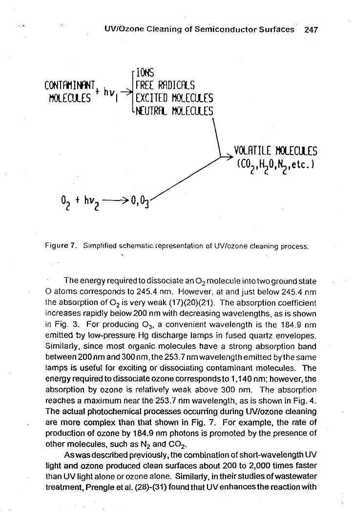
The available evidence indicates that UV/ozone cleaning is primarily e result of photosensitized oxidation processes, as is represented sche- atically in Fig. 7. The contaminant molecules are excited and/or dissoci- ed by the absorption of short-wavelength UV light. Atomic oxygen and :one are produced simultaneously when 0, is dissociated by the absorp- In of UV with wavelengths less than 245.4 nm. Atomic oxygen is also oduced when ozone is dissociated by the absorption of the UV and longer ivelengths of radiation (20)(21). The excited contaminant molecules and e free radicals produced by the dissociation of contaminant molecules act with atomic oxygen to form simpler, volatile molecules, such as CO,, !O, and N,.
0
F i g u n
0 ato- the at. incre2 in Fig emittc Simil: betwe lamps energ- absorl reach4 The a: are m produl other
I: light a, than L treatn
. .
I
.. (L UWOzone Cleaning of Semiconductor Surfaces 247
r CONTFWIMC)(T, hv
HOLE CUES
VOLHTILE WECUES (C02,t$0,+,etc. 1
Figure 7. Simplified schematic representation of UVIozone cleaning process ,
The energy required to dissociate an 0, molecule into two ground state 0 atoms corresponds to 245.4 nm. However, at and just below 245.4 nm the absorption of O2 is very weak (17)(20)(21). The absorption coefficient increases rapidly below 200 nm with decreasing wavelengths, as is shown in Fig. 3. For producing O,, a convenient wavelength is the 184.9 nm emitted b y low-pressure Hg discharge lamps in fused quartz envelopes. Similarly, since most organic molecules have a strong absorption band between 200 nm and 300 nm, the 253.7 nm wavelength emitted by the same lamps is useful for exciting or dissociating contaminant molecules. The energy required to dissociate ozone corresponds to 1,140 nm; however, the absorption by ozone is relatively weak above 300 nm. The absorption reaches a maximum near the 253.7 nm wavelength, as is shown in Fig. 4. The actual photochemical processes occurring during UWozone cleaning are more complex than that shown in Fig. 7. For example, the rate of production of ozone by 184.9 nm photons is promoted by the presence of other molecules, such as N2 and CO,.
As was described previously, the combination of short-wavelength UV light and ozone produced clean surfaces about 200 to 2,000 times faster than UV light alone or ozone alone. Similarly, in their studies of wastewater treatment, Prengle et al. (28)-(31) found that UV enhances the reaction with

248 Handbook of Semiconductor Wafer Cleaning Technology
ozone by a factor of lo2 to lo4 , and the products of t h e reactions are materials such as CO,, H,O, arid N, lricreasing the temperature increased the reaction rates
The physical and chemical mechanisms of hydrocarbon removal by UV/ozone cleaning was studied in an integrated processing facility with in situ analysis capabilities (44). On silicon wafers intentionally contaminated with heptanol, volatilization of the hydrocarbons appeared to proceed by means of oxidation of the long carbon chain at every carbon atom. In the final stage of the process, the carbon desorbed as CO, (but some carbon containing species remained on the surface). The desorbing gases were found to,be mostly CO, and H,O. UV/ozone cleaning at elevated (>6OoC) temperature resulted not only in more complete hydrocarbon removal but also in the removal of surface OH-groups.
Mattox (45) found that mild heat increases the UV/ozone cleaning rates. Bolon and Kunz (l), on the other hand, found that the rate of ozone depolymerization of photoresists did not change significantly between 1 OOOC and 300OC. The rate of destruction of microorganisms was similarly insensitive to a temperature increase from room temperature to 4OoC (32). One manufacturer of UV/ozone cleaning equipment claims that the rate of photoresist stripping by UV/ozone increases several-fold as the tempera- ture is raised from 20°C to 3OOOC (43)
5.0 UVIOZONE CLEANING IN VACUUM SYSTEMS
Sowell et al. (2) reported that, when torr pressur-e of oxygen was present in a vacuum system, short-wavelength UVdesorbed gases from the walls of the system. During .UV irradiation, the partial pressure of oxygen decreased, while that of CO, and H,O increased. Similar results were obtained by Hiroki et at. who found that upon tuming on a short-wavelength UV lamp in a vacuum chamber, the outgassing of "H,, CO. CO,, CH,. etc increased, while H,O and 0, were slightly reduced" (46).
When UVlozone cleaning of silicon surfaces in air was compared with UV/ozone cleaning in one to 20 torr of pure oxygen in a vacuum chamber, it was found that, whereas a clean surface could be produced in 7 seconds in air, it took about 50 minutes to produce the same cleanliness level in 5 torr of oxygen. It took 60 minutes in 20 torr of oxygen, and no cleaning effect was observed in 1 torrafter 60 minutes of cleaning (47). (It should be noted, however, that the cleaning conditions differed. In the air cleaning, the UV Source was 1 cm from the sample. In the vacuum chamber, the UV source
1 : , -
W;
be
va
I iq a \ uc I ig t h; at( na
sy! en to> va xe U1 wir of
oz
OP siv mc so1 so1
ha in *
6.0
sal' wh bo;
de:, dol

UV/Ozone Cleaning of Semiconductor Surfaces 249
I
i
I
was 6 cm from the sample and the UV passed through a quartz window before reaching the sample.)
A UV/ozone cleaning method that is suitable for use in an ultrahigh vacuum environment uses a low pressure Hg UV lamp and a separate O L O I I ~ source (48). The ozone, generated In an oxygen glow dlscharge at liquid nitrogen temperatures, is admitted into the vacuum chamber through a valve. A slow cleaning action was observed at a 2 x IOe5 torr pressure. Using the same ozone source, cleaning was also observed without the UV light when the sample was heated to 500K (227OC). The ozone molecules that reach the sample surface decompose on the heated surface. The atomic oxygen created by the decomposition can react with the contami- nant molecules.
One must exercise caution in using a mercury UV source in a vacuum system because, should the lamp envelope break or leak, mercury can enter, ruin the usefulness of the system and cause hazards due to its toxicity. Mercury has a high vapor pressure; its complete removal from a vacuum chamber is a difficult task. Other types of UV sources, such as xenon or deuterium lamps, may be safer to use in vacuum systems. The UV light can also be radiated into systems through sapphire or quartz windows, or through deep-UV fiber optic bundles. A small partial pressure of oxygen should be present during UV cleaning.
Caution must also be exercised when using UV/ozone in a cry- opumped vacuum system, since cryopumped ozone is potentially explo- sive (49), particularly during regeneration of the cryopump. A convenient method of dealing with this potential hazard is to use two kinds of UV sources, one an ozone-generating source, the other an "ozone killer" source (50), as discussed in the next section.
Integrated processing systems, which incorporate UV/ozone cleaning, have been proposed (44)(51)-(53) and built (54)-(56) for processing devices in vacuum or in controlled atmospheres.
6.0 SAFETY CONSIDERATIONS
In constructing a UV/ozone cleaning facility, one must be aware of the safety hazards associated with exposure to short-wavelength UV light which can cause serious skin and eye injury within a short time. In the UV boxes used by Vig et al., switches are attached to the doors so that when the doors are opened the UV lamps are shut off automatically. If the application demands that the UV lamps be used without being completely enclosed (for
250 Handbook of Semiconductor Wafer Cleaning Technology
example, as might be the case if a UV cleaning facility is incorporated into a wire bonder), then proper clothing and eye protection (e.g., UV safety glasses with side flaps) should be worn to prevent skin and eye damage
Short-wavelength U V radiation is strongly absorbed by human cellular DNA. The absorption can lead to DNA-protein crosslinks, and can result in cancer, cell death, and cell mutation. It is now well-known that solar UV radiation is the prime causative factor in human skin cancer (57)(58), and is a significant risk factor in eye cancer (59). The 290 - 320 nm portion of solar UV radiation has been found to be the most effective wavelength region for causing skin cancer. Because the atmosphere filters out the shorter wavelengths, humans are not normally exposed to wavelengths as short as 254 nm. However, in a study of the effects of UV radiation on skin cancerrates, i t was found that the 254 nm wavelength was many times more effective in causing cell mutations than were those above 300 nm wave- lengths. Therefore, it IS essential that personnel not be exposed to the short wavelengths needed for UWozone cleaning because even low doses of these wavelengths can cause significant damage to human cells. Safety exposure limits for ultraviolet germicidal irradiation have been set by the American Conference of Governmental and Industrial Hygienists (7)(60).
Another safety hazard is ozone, which is highly toxic. In setting up a UV cleaning facility, one must ensure that the ozone levels to which people are exposed do not exceed 0.1 ppm TWA and 0 3 ppm STEL (61). The time weighted average (TWA) exposure is a person's average airborne expo- sure in any 8 hour work shift of a 40 hour work week. The short term exposure limit (STEL) is a person's 15 minute time weighted average exposure which is not to be exceeded at any time during a workday. Ozone is a potential hazard in a cryopumped vacuum system because cryopumped Ozone can become explosive under certain conditions (49).
One method of minimizing the hazards associated with ozone is to use two types of short-wavelength ultraviolet sources for UV/ozone cleaning (SO): one, an ozone-generating UV lamp, e.g , a low-pressure mercury itght in a fused quartz envelope, the other, a UV lamp that does not generate ozone but which emits one or more wavelengths that are strongly absorbed by ozone, e.g., a low-pressure mercury light in a high-silica glass tube which emits at 253.7 nm but not at 184.9 nm. Such a non-ozone generating UV source can be used as an "ozone killer." For example, in one cryopumped vacuum system, UWozone cleaning was performed in up to 20 torr of oxygen. After the cleaning was completed and the ozone-generating UV lamp was tumed off, ten minutes of "ozone killer" UV fight reduced the concentration of ozone to less than 0.01 ppm, a level that is safe for
I i
I i
!
I
i
i
i f
i ! i 1
.
cryopul t fa t 1 o ns Wit hou! (63).
Tt- use of c< found tc ing heac aircraft ozone c the low I
7.0 CC
Thi facility : Polishec Alzak (8; conduct i reflector poor ref1
lnit UV box ( in time, i appearel Alzak, a1 probably should bc ity of par in avoidii coating ; interior s able UVh date, no ref lecta n percent (
example. be replac

UV/O+one Cleaning of Semiconductor Surfaces 251
cryopumping (62) Therefore, with the “ozone killer’’ lamp, ozone concen- trations were reduced by at least a factor of one hundred within ten minutes. Without the “ozone killer’’ lamp, the half-life of ozone is three days at 2OoC
(6 3) Thedecomposition ofozonecan also begreatlyaccelerated throughthe
use of catalysts. For example, prior to 1980, in high-flying aircraft, ozone was found to be a causative factor for flight personnel and passengers experienc- ing headaches, eye, nose and throat irritations and chest pains. Passing the aircraft cabin air through a precious-metal catalytic converter reduced the ozone concentration from the 1 - 2 ppm level present in the troposphere to the low levels required for passenger comfort and safety (64).
!
~
7.0 CONSTRUCTION OF A UV/OZONE CLEANING FACILITY
The materials chosen for the construction of a UV/ozone cleaning facility should remain uncorroded by extended exposure to UV/ozone Polished aluminum with a relatively thick anodized oxide layer, such as Alzak (8), is one such material. It is resistant to corrosion, has a high thermal conductivity, which helps to prevent heat buildup, and is also a good reflector of short-wavelength UV. Most other metals, including silver, are poor reflectors in this range.
Initially, Vig et ai. used an ordinary shop-variety aluminum sheet for UV box construction, which was found not to be a good material because, in time, a thin coating of white powder (probably aluminum oxide particles) appeared at the bottom of the boxes. Even in a UV box made of standard Alzak, after-a couple of years’ usage, white spots appeared on the Alzak, probably due to pinholes in the anodization. The UV/ozone cleaning system should be inspected periodically for signs of corrosion to avoid the possibil- ity of particles being generated. The use of “Class M” Alzak may also aid in avoiding particle generation, since this material has a much thicker oxide coating and is made for “exterior marine service,” instead of the “mild interior service” specified for standard Alzak. Some commercially avail- able UVlozone cleaners are now constructed of stainless steel (65)(66). To date, no corrosion problems have been reported with such systems. The reflectance of stainless steel in the 200 to 250 nm range is about twenty percent (7).
Organic materials should not be present in the UV cleaning box. For example, the plastic insulation usually found on the leads of UV lamps must be replaced with inorganic insulation such as glass or ceramic. The box
1

252 Handbook of Semiconductor Wafer Cleaning Technology
should be enclosed so as to minimize recontamination by circulating air, arid to prevent accidental U V exposure and ozone escape.
The most widely available sources of short-wavelength UV light are the mercury arc lamps. Low-pressure mercury lamps in pure fused quartz envelopes operate near room temperature, emit approximately 90 percent at the 253.7 nm wavelength, and generate sufficient ozone for effective surface cleaning. Approximately five percent of the output of these lamps is at 184.9 nm. Medium- and high-pressure UV lamps (1 7) generally have a much higher output in the short-wavelength UV range. These lamps also emit a variety of additional wavelengths below 253.7 nm, which may enhance cleaning action. However, they operate at high temperatures (the envelopes are near red-hot), have a shorter lifetime, higher cost, and present a greater safety hazard. The mercury tubes can be fabricated in a variety of shapes to fit different applications. In addition to mercury arc lamps, microwave-powered mercury vapor UV lamps are also available
Other available sources of short-wavelength UV include xenon lamps and deuterium lamps. These lamps must also be in an envelope transpar- ent to short-wavelength UV, such as quartz orsapphire, if no separate ozone generator is to be used. In setting up a UV cleaning facility, one should choose a UVsource which will generate enough UV/ozone to allow for rapid photosensitized oxidation of contaminants. However, too high an output at the ozone-generating wavelengths can be counterproductive because a high concentration of ozone can absorb most of the UV light before it reaches the parts to be cleaned. The parts should be placed as close to the UV source as possible to maximize the intensity reaching them. In the UV cleaning box 1 of Vig et al., the parts to be cleaned were placed on an Alzak stand the height ofwhich can be adjusted to bring them close to the UVlamp. The parts to be cleaned can also be placed directly onto the tube if the box is built so that the tube is on the bottom of the box (68).
An alternative to using low-pressure mercury lamps in fused quartz envelopes is to use an arrangement similar to that of box 2, shown in Fig. 1. Such a UWozone cleaner, now also available commercially (43), uses silent-discharge-generated ozone and a UVsource that generates the 253.7 nm wavelength, as is shown in Fig. 5. The manufacturer claims a cleaning rate that is much faster than that obtainable with UV/ozone cleaners that do not contain separate ozone generators. This cleaner also uses oxygen from a gas cylinder and a built-in sample heater that may further increase the cleaning rate.
(67) -
I
E
€
UV/Ozone Cleaning of Semiconductor Surfaces 253
I
8.0 APPLJCATIONS
to reduce the potential for contamination by the metallic impurities present in H202. “The cleanest silicon surface with respect to metallic and hydrocarbon impurities was achieved with a HF etch-H,O rinse-UWozone oxidation process.”
In another study, high resolution electron energy loss spectroscopy (HREELS) and other high sensitivity surface analytical techniques were
8.1 Cleaning of Silicon Surfaces
I

254 Handbook of Semiconductor Wafer Cleaning Technology
~ s t d to investigate the mechanisms of hydrocarbon removal from Si wafers by UV/ozone and other cleaning techniques (82). A drop of a hydrocarbon (cyclohexane) was spun onto an HF-dip cleaned Si(100) surface. After the HF-dip cleaning, the surface was found to be hydrogen-passivated, i.e., saturated with SiH and SiH, groups. The adsorbed hydrocarbons did not replace the surface hydrogen, but adsorbed molecularly on top of the hydrogen. During the first 45 to 60 seconds of UV/ozone cleaning, at room temperature, very rapid oxidation of the Si surface occiirred, and the hydrogen that saturated the surface after the HF dip was transformed into OH groups. Since hydrocarbons were still present at the end of this initial cleaning period, the oxidation apparently occurred underneath the contami- nant layer. The UV/ozone treatment transformed the previously hydropho- bic surface into a hydrophilic surface.
HREELS was also used to compare an RCA cleaned Si(lO0) surface with a UV!ezone c!eanec! one (82). The spectra! signatures of the two surfaces were “very much alike”. The authors conclude that “The UV-0, process is a gas-phase process that creates an oxide very similar to that after the standard RCA wet surface clean. The UV-0, process also removes hydrocarbons with similar efficiency as the RCA clean. Pending further study of metal removal, the UV-0, process seems a viable gas- phase replacement for the RCA clean” (82).
When several variations of HF treatments were examined for suitabil- i ty as pretreatment for a silicon epitaxy process, the optimum treatment consisted of the steps of HF dipping, deionized water rinsing, nitrogen gas blowing for drying, and UV/ozone cleaning (77).
In the production of high-quality epitaxial films by molecular beam epitaxy (MBE), the cleaning of substrate surfaces is one of the most important steps. UV/ozone cleaning of silicon substrates in silicon MBE has been found to be effective in producing near defect-free MBE films (47)(81) (84)-(87). By using UV/ozone cleaning, the above 12OOOC temperatures required for removing surface carbon in the conventional method can be lowered to well below 1 OOO°C. The slip lines resulting from thermal stresses and thermal pitsthat are often produced by the high-temperature treatment are minimized4n the lower temperature processing. Impurity redistribution in the substrate is also reduced.
Vacuum ultraviolet (VUV) light from a synchrotron source has been used in the low temperature cleaning of HF-passivated Si surfaces (88). In another study, VUV from a microwave-excited deuterium lamp was used in low-temperature (Le., 65OOC) silicon epitaxial growth (89). Organic con- tamination was effectively removed from Si, GaAs and MgF2 substrates by
i
i I i I
I I
i i
i j
t
!
I
P
1
t -
I 5
) I
S
UV/Ozone Cleaning of Semiconductor Surfaces 255 .
124 nm VUV cadlatior1 fr‘onl a kryptoil !,Zzice at 0 5 - 760 ? O J I - of air pressure (90). During Si molecular beam epitaxy, UV radiation from 193 nm ArF or 248 nm KrF lasers were found to enhance the interdiffusion of Si and B,O,, S b incorporation, and t i le Hdll r i ~ ~ t J l l l c ) \.-
A two-step annealing method has been used to reduce the leakage currents in 64 Mbit silicon dynamic random-access memory chips (92). The first annealing step is at 3OOOC while the wafers are exposed to UV/ozone, and the second is at 8OOOC in dry oxygen.
Iri the processing of semiconductor wafers, a single UV/ozone expo- sure has been found to be capable both of “descumming” and of stabilizing (93). After developing and rinsing the photoresist pattern, the UV/ozone removes the thin layers of organic photoresist residue (scum) from the “clear” regions. The photoresist stabilization is believed to be due to crosslinking produced by the short-wavelength (deep) UV radiation (94). The stabilization rate is accelera!ed by increasing the temperature. For example, UV/ozone exposure times of 10 to 30 minutes from a 25 cm x 25 cm low-pressure mercury grid lamp at 1 OOOC yields satisfactory results. The stabilized photoresist pattern exhibits (i) improved adhesion to the sub- strate, (ji) improved ability to maintain geometrical shape under thermal stress, and (iii) improved ability to withstand exposure to the etchants and solvents used to create the desired patterns in the circuit coatings (93).
UV/ozone cleaning bas also been used in studies of the wetting of silicon and silica wafers (95)-(I 02). These studies included investigations of the evolution of tiny drops of polydimethylsiloxane and squalane on UV/ ozone cleaned Si wafers, and the dynamics of ultra-thin wetting firms under a controlled atmosphere. UV/ozone cleaning was also used in studies of surface-chemical reactions (1 03), and in the formation of diblock copolymer films on silicon wafers (104).
The use of UV/ozone treatment for the removal of contaminants from thin film transistors, and from substrates of complex composition or geome- tries has also been studied (105). Surfaces that were not directly irradiated by the UV became clean, but the required cleaning time was longer, in agreement with earlier results (3)-(6) on cleaning by UWozone vs. ozone alone. The chemistry of oxidized hydrocarbons on 90, was found todiffer from that on gold; UVlozone was able to remove hydrocarbons from Si02 much faster than from gold. On thin film transistors, the UWozone cleaned the field oxide regions faster than the single component surfaces (105).
UV/ozone cleaning has been used in a variety of silicon processing studies. It was used as a precleaning step in investigations of: remote plasma cleaning using a hydrogen plasma (1 06), the breakup upon anneal-

256 Handbook of Semiconductor Wafer Cleaning Technology , -
ing of a thin oxide film between a polysilicon film and the silicon substrate (IO?), t he effect of UV irradiation on minority-carrier recombination lifetime (IO@, and the chemical vapor deposition of titanium nitride onto silicon wafers (1 09)
8.2 Cleaning of Other Semiconductor Surfaces
UV/ozone cleaning has also been applied to the cleaning of gallium arsenide (GaAs) wafers (I 10)-(122), and to cleaning and “ozone etching” of indium phosphide (InP) substrates (122)-(126). In the growth of GaAs by molecular beam epitaxy and by chemical vapor deposition (CVD) substrate cleanliness is critically important. Contamination of the substrate/epitaxial layer interface leads to defects that reduce the yield of functional devices. Carbonaceous contamination is the primary problem. UV/ozone has been shown to be an effective means of removing carbonaceous contamination and, at the same time, producing an oxide-passivated surface (1 IO). The carbon-free oxide can be removed by heating in ultrahigh vacuum prior to MBE layer growth.
The formation of a sacrificial oxidelayer on GaAs is a well established step in the preparation of in situ cleaned substrates prior to MBE. A problem with oxides formed in air or in deionized (DI) water is that the oxide tends to be Ga rich, with As pile-up at the oxide/GaAs interface. .When such an oxide is thermally desorbed, the stoichiometry of the surface is not preserved and the MBE layer is, thereby, degraded. In UV/ozone produced oxide layers, the As/Ga ratios and the As-oxide/Ga-oxide ratios are much closer to unity than for other oxidation methods (1 11)(118)(122). In the same amount of time, the‘UV/ozone also produces a much thicker oxide layer than air exposure. For example, in ten minutes, UV/ozone produces a 2.0 nm to2.5 nm oxide layer. In air alone, 24 hoursare required to produce the same thickness. A longer oxidation time increases the amount of adsorbed and absorbed carbonaceous contamination. The contamination rate of a UWozone produced oxide surface was found to be “at least an order of magnitude less” than that of a DI water produced oxide surface when obsewed for days in an x-ray photoelectron spectroscopy (XPS) $stem (I I 1).
A problem with AIGaAsIGaAs heterostructure field effect transistors (HFETs) is sidegating, Le., the electrical interaction between two closely spaced devices which were intended to be isolated from each other. Sidegating was traced to carbon contamination, presumably due to the adsorption of carbonaceous contamination from the atmosphere. When
1
11 C
S
C
C e t f( f l
tl d a l- v I 4
n 1 1
t l
9
v\
S
v\
C
P e t t I 1
8

UV/Ozone Cleaning of Semiconductor-Surfaces- 257
UV/ozone cleaning was compared with other methods, “The carbon con- centration of the interfacial region decreased by two orders of magnitude for the wafers exposed to ultraviolet radiation.. .A dramatic improvement in sidegating was observed for the wafers subjected to the ultraviolet-ozone cleaning procedure.” (1 14). Similarly, another study found that “Ultraviolet/ ozone cleaning of GaAs substrates prior to metalorganic molecular beam epitaxy at 5OOOC is shown to reduce the interfacial C and 0 concentrations by more than two orders of magnitude ... UV/ozone cleaning...is a necessity for obtaining MESFET performance undegraded by parallel conduction from the substrate-epitaxlal layer interface.” (I 18).
In a study of light-enhanced oxidation of GaAs surfaces, it was found that photon energies higher than 4.1 eV (which is the energy needed to dissociate 0, )greatly enhanced the oxidation rate (1 17). The temperature at which the oxide desorbs from GaAs surfaces was found to be 638OC for UV/ozone produced oxide vs. 582OC for thermally produced oxide (120). When the native oxide and Fermi level of UV/ozone formed oxides on GaAs were investigated (I 27), it was found that the surface oxide consisted of a mixture of .gallium and arsenic oxide phases which desorb at two different temperature ranges. Desorption of arsenic oxide phases and oxygen transfer from arsenic to gallium occurred at 250 - 5OO0C, and desorption of gallium oxide phases occurred at 550 - 600OC.
Oxide passivation with UWozone followed by thermal desorption also works well on InP. Epitaxial growth has successfully been carried out on InP surfaces so cleaned (1 22)(123). When the native oxides on InP surfaces were compared after solvent cleaning, etching with two different wet chemical etchants, and “ozone etching” with UV/ozone, the surface com- positions were found to vary greatly with the surface treatment. The ozone- etched surface contained the most oxygen, and the In:P ratio increased as the surface treatment became more oxidizing (124). The oxides grown on InP can improve the electrical properties of InP interfaces (123).
8.3 Other Applications
The UWozone cleaning procedure is now used in numerous applica- 1
tions in addition to the cleaning of semiconductor surfaces. A major use is substrate cleaning prior to thin film deposition. The process is also being applied in a hermetic sealing method which relies on the adhesion between clean surfaces in an ultrahigh vacuum (14)(51)(128)(129). It has been shown that metal surfaces will weld together under near-zero forces if the surfaces are atomically clean. A gold gasket between gold metallized (UV/
258 Handbook of Semiconductor Wafer Cleaning Technology
ozone cleaned) aluminum oxide sealing surfaces is currently providing excellent hermetic seals in the production of a ceramic flatpack enclosed quartz resonator. It has also been shown (51)(128)(129) that it is feasible to achieve hermetic seals by pressing a clean aluminum gasket between two clean, unmetallized aluminum oxide ceramic surfaces.
The same adhesion phenomenon between UV/ozone cleaned gold surfaces has been applied to the construction of a novel surface contami- nant detector (1 30)(131). The rate of decrease in the coefficient of adhesion between freshly cleaned gold contacts is used as a measure of the gaseous condensable contaminant level in the atmosphere.
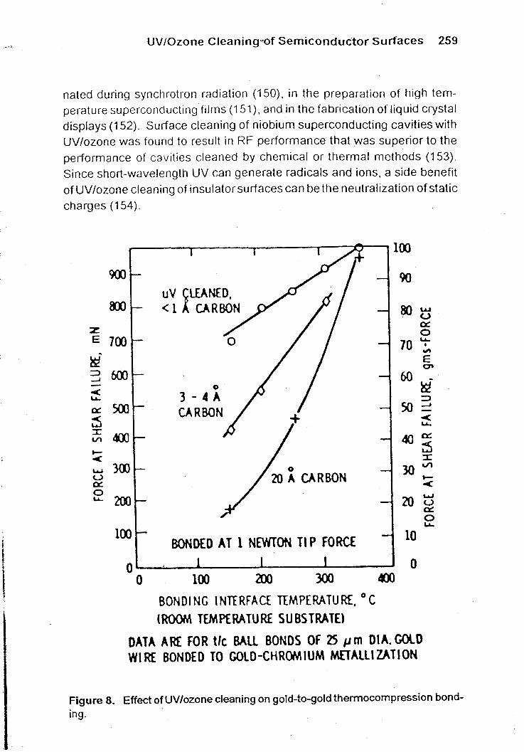
The process has also been applied to improve the reliability of wire bonds, especially at reduced temperatures. For example, it has been shown (1 32)(133) that the thermocompression bonding process is highly tempera- ture dependent when organic contaminants are present on the bonding surfaces. The temperature dependence can be greatly reduced by UV/ ozone cleaning of the surfaces just prior to bonding, as is shown in Fig. 8. In a study of the effects of cleaning methods on gold ball bond shear strength, UV/ozone cleaning was found to be the most effective method of cleaning contaminants from gold surfaces (1 34). UV/ozone is also being used for cleaning alumina substrate surfaces during the processing of thin film hybrid circuits (1 35).
A number of cleaning methods were tested when the nonuniform appearance of thermal/flash protective electro-optic goggles was traced to organic contaminants on the electro-optic wafers. UV/ozone proved to be the most effective method for removing these contaminants, and thus it was chosen for use in the production of the goggles (136).
Other applications have been: photoresist removal (1)(6)(13)(43), the cleaning of vacuum chamber walls (2), photomasks (69), lenses (69), mirrors (69), solar panels (69), sapphire (69) (before the deposition of HgCdTe) and other fine linewidth devices (69)(70)(137), inertial guidance su bcomponents (glass, chromium-oxide surfaced-gas bearings, and beryl- lium) (69)(138), the cleaning of stainless steel for studying a milk-stainless steel interface (139), the cleaning of amorphous alloy Metglas 2826 (140) and of sintered beryllium oxide (141), the cleaning of adsorbed species originating from epoxy adhesives (IS), the removal of organic materials deposited during the deposition of antireflective silica coatings (1 42), the cleaning of surfaces prior to the deposition monolayer films (143)-(145), in a study of the frictional behavior of thin film magneticdisks (146), in friction studies in ultrahigh vacuum (147)(148), in studies of the spreading of liquid dcoplets (1 49), the cleaning of an x-ray grating which was carbon contami-
nated ( per at u r display. uv/ozo perforn Since s of uv/o charge:
Figure t ing.
UV/Ozone Cleaning.-of Semiconductor Surfaces 259
!
nated during synchrotron radiation (150), in the preparation of high tem- perature superconductlng films (1 51), and in the fabrication of liquid crystal displays (1 52). Surface cleaning of niobium superconducting cavities with UV/ozone was found to result in RF performance that was superior to the performance of cavities cleaned by chemical or thermal methods (153). Since short-wavelength UV can generate radicals and ions, a side benefit of UV/ozone cleaning of insulatorsurfaces can be the neutralization ofstatic charges (1 54)
BON
60NDED AT 1 NEWTON T I P FORCE
0 1 I 1
100
90
8% p: 0
0 100 m 300 400 BONDING INTERFACE TEMPERATURE, O C
(ROOM TEMPERATURE SUBSTRATE)
DATA A N FOR tlc MU BONDS OF 25 p m OM. GOLD WIR€ BONDED TO COLD-CHRWIUM M A L L I U T I O N
Figure 8. Effect of UV/ozone cleaning on gold-to-gold thermocompression bond- ing.

260 Handbook of Semiconductor Wafer Cleaning Technology
9.0 EFFECTS OTHER THAN CLEANING
Short-wavelength UV, ozone, and the combination of the two can have effects other than surface cleaning The more significant of these effects are discussed below.
9.1 Oxidation
Ozone’s oxidation power is second only to that of fluorine. Ozone can oxidize most inorganic compounds to their final oxidative state (63). For most substrates, UV/ozone cleaning, for the minimum time necessary to obtain a clean surface, will not cause a significant amount of oxidation. However, extended storage under UV/ozone may be detrimental for some oxidizable surfaces. In some cases, the enhanced oxide formation may be beneficial. For example, whereas the “native” oxide on GaAs is only about 3 nm thick, UV/ozone produces an oxide layerthat is 10 - 30 nm thick (1 12), i.e., UVJozone can produce a clean, oxide passivated surface. Similarly, the native UV/ozone-produced oxide layer at the interface of HgCdTe/SiO, has been found to enhance the interface properties (155). Solar radiation and atmosphericozone have been found to markedly enhance the sulfidation of copper (156). Extended exposure to UWozone has been found to significantly increase the oxide layer thicknesson aluminum surfaces (1 57). Whereas the oxide thickness on air-exposed aluminum surfaces is normally limited to about 50 A, UV/ozone exposure increased the oxide layer thickness significantly beyond the “normal” 50 A limit, as shown in Table 4.
Table 4. UV/Ozone Exposure vs. Oxide Thickness on Aluminum
Substrate treat men t Oxide thickness (A) Evaporate lpm of aluminum 47
10-minute UV/ozone cleaning 90
60-m i n u t e U Wozon e cleaning 200
When the oxidation of silicon surfaces was studied by Auger electron spectroscopy, it was found (72) that “an etched silicon surface can be exposed to air for about 1 hour without showing the silicon oxide signal at 82 eV. Under the UV/ozone treatment a rapid oxidation takes place. The
*
,-
PI TI th 01
th A1
dt th O> wl be
9.
Oi
gl. of e\
e>; bc
9.
S 2
re
hY su
fa- t h su U\ Of.
ef to ce to

UV/Ozone Cleaning of Semiconductor Surfaces 261
peak characteristic of silicon oxide appears after one minute of irradiation. The increase of the intensity of this peak gives evidence for a thickening of the layer."Ten minutes of UV/ozone cleaning increased the oxide thickness on oxidized silicon substrates from 0.9 nm to 1.2 nm (85).
The ozone produced by a UWozone generator was found to enhance the growth rate of 30, during the thermal oxidation of Si at 8OOOC (75). After a 140 minute oxidation period, the SO, film thickness was 290 a with ozone vs. 148 A without ozone. The oxide growth rate enhancement decreased at higher temperatures and longer exposure times (Le., with thicker films), presumably because "during the initial stage of silicon oxidation, the reaction at the silicon surface may be the controlling factor, whereas in the later stage, the diffusion of reactant through the oxide layer becomes important."
1
t
9.2 UV-Enhanced Outgassing
Short-wavelength UV has been found to enhance the outgassing of glasses (1 58). The UV light produced the evolution of significant quantities of hydrogen, water, carbon dioxide, and carbon monoxide. The hydrogen evolution was proportional to the amount of radiation incident on the samples. For UV-opaque glasses, the evolution occurred from the side exposed to the UV; for high-transmission samples, the gas evolved from both sides.
9.3 Other Surface/lnterface Effects
Energetic radiation such as UV and gamma radiation has been reported to produce dehydration and the formation of free radicals on silica surfaces (1 59). However, dehydrated (or siloxinated) silica surfaces are hydrophobic (1 60)(161), whereas UV/ozone-cleaned silica (quartz) sur- faces exhibit a very low (less than 4') water contact angle, thus indicating that the UV/ozone does not dehydrate the surfaces, nor does it modify surface silanol groups the way high temperature vacuum baking does(l62). UV/ozone has been shown to convert hydrophobic surfaces into hydrophilic ones. Short-wavelength UV has also been found to produce a bleaching effect in Si-Si, interfaces with thin oxides (163), and has also been found to produce yellowing (color centers) during the cleaning of aluminum oxide ceramics (39). The yellowing can be readily bleached by heating thesample to above 160OC.
262 Handbook of Semiconductor Wafer Cleaning Technology
9.4 Etching
Short-wavelength (1 93 nm) UV laser irradiation of biological and polymeric materials has been shown to be capable of etching the materials with great precision, via “ablative photodecomposition,” and without signifi- cant heating of the samples. Linewidths 5 pm wide have been etched onto a plastic film to demonstrate the capability of this technique (164). Oxygen does not appear to have the same significance in this process as it does in UV/ozone cleaning. The etch depth vs. fluence in vacuum and in air were found to be the same (165).
In a study of the photodegradation of polyimide films, it was found that “the complete photooxidation process requires photolysis with light below 300 nm to produce both chain scission and photooxidative ablation effi- ciently,” in the presence of oxygen (166).
UV light of wavelengths less than 200 nm has been proposed for selectively removing biological materials, e.g., skin lesions and decayed teeth (167). UWozone has been found to etch Teflon (39)(40), and Viton (39), and will likely etch other organic materials as well (168)(169). The susceptibility of polymers to degradation by ozone can be reduced by various additives and through the elimination of “the offending double bonds from the backbone structure of the polymers” (170). Vacuum ultraviolet radiation has been used to form images in polymer films (171)(172). Photoetching of polymer films with soft x-rays h a s also been studied (1 73). The etching of polymethyl mathacrylate (PMMA) by UV and VUV has also been investigated (174).
10.0 SUMMARY AND CONCLUSIONS
The UV/ozone cleaning procedure has been shown to be a highly effective method of removing a variety of contaminants from silicon, and compound semiconductor wafers, as well as from many other types of surfaces. It is a simple-to-use dry process that is inexpensive to set up and operate.. It can produce clean surfaces at room temperature, either in a room atmosphere or in a controlled atmosphere. “The UV-0, process is a gas-phase process that creates an oxide very similar to that after the standard RCA wet surface clean. The UV-0, process also removes hydrocarbons with similar efficiency as the RCA clean” (82).
In combination with a dry method for removing inorganic contamina- tion, such as cleaning with UV-excited high purity chlorine gas (175), the
UV/Ozone Cleaning of Semiconductor surfaces 263
method may meet the requirPmen!P fp: the all-drj cleaiili KJ illctiiodsttiat will be necessary for processing of future generations of semiconductor de- vices. When compared with plasma cleaning, UV/ozone cleaning produces less radiation damage and is more controllable (81).
The variables of the UV cleaning procedure are the contaminants initially present, the precleaning procedure, the wavelengths and intensity emitted by the UVsource, the atmosphere between the source and sample, the distance between the source and sample, and the time of exposure. For surfaces that are properly precleaned and placed within a few millimeters of an ozone-producing UV source, the process can yield a clean surface in 1
t less than one minute. The combination of short-wavelength UV plus ozone produces a clean surface substantially faster than short-wavelength UV without ozone or ozone without UV light. Clean surfaces will remain clean indefinitely during storage under UWozone, but prolonged exposure of oxide-forming metals to UWozone in roon? air can produce rapid corrosion.
The cleaning mechanism seems to be a photosensitized oxidation process in which the contaminant molecules are excited and/ordissociated by the absorption of short-wavelength UV. Simultaneously, atomic oxygen is generated when molecular oxygen is dissociated and when ozone is dissociated by the absorption of short and long wavelengths of radiation. The products of the excitation of contaminant molecules react with atomic oxygen to form simpler molecules, such as CO, and H,O, which desorb from the surfaces.
i i i 1 ?
!
i
i
REFERENCES
1.
2.
i
?
Bolon, D. A. and Kunz, C. O., J. of Polymer Engin. Sci. 121109-111 (1 972)
Sowell, R. R., Cuthrell, R. E., Mattox, D. M., and Bland, R. D., J. Vac. Sci. Techno/. 1 1 :474-475 (1 974) I
3 'dig, J. R., Cook, C. F. Jr., Schwidtal, K., LeBus, J. W., and Hafner, E., in: Proc. 28thAnn. Symp. on Frequency Control, Philadelphia, PA, AD 011113, pp. 96-108 (1974)
4. Vig, J. R., LeBus, J. W., and Filler, R. L., in: Proc. 29fhAnn. Symp. on Frequency Control, Philadelphia, PA, AD A01 7466, pp. 220-229
Vig, J. R., /E€€ Transactionson Parts, Hybrids, andpackaging, PHP- 12(4):365-370 (December 1976)
(1 975)
5 . I ~
264 Handbook of Semiconductor Wafer Cleaning Technology
6. Vig, J. R , in Trealise on Clean Surface Technolnm ? (K !- M~ttai , ecf ) , pp. 1-26, Plenum Press, NY (1987)
7. Sylvania Engineering Bulletin 0-342, "Germicidal and Short-Wave Ultraviolet Radiation," GTE Products Corporation, Sylvania Lighting Center, Danvers, Massachusetts 01 923 (1 981)
8. Alzak is an aluminum reflector material with a corrosion-resistant oxide coating. The Alzak process is licensed to several manufacturers by the Aluminum Co. of America, Pittsburgh, PA 15219
9. Model No. R-52 Mineralight Lamp, UVP, lnc., San Gabriel, CA 91 778.
10. See, e.g., Encyclopaedic Dictionary of Physics, 5:275, Pergamon Press, New York (1 962)
11. Schrader, M. E., in: Surface Contamination: Its Genesis, Detection and Control, (K. L. Mittal, ed.), 2541-555, Plenum Press, New York
12. Bryson, C. E., and Sharpen, L. J., in: Surface Contamination: Its Genesis, Detection and Control, (K. L. Mittal, ed.), 2:687-696, Plenum Press, New York (1 979)
13. Holloway, P. H., and Bushmire, 0. W., in: Roc. 12th Ann. Reliability Phys. Symp., pp. 180-186, IEEE,'Piscataway, NJ (1974)
14. Peters, R. D., in: Proc. 30th Ann. Symp. 017 Frequency Control, pp 224-231, Philadelphia, PA, AD A046089 (1 976)
15. Benson, R. C., Nall, 8. H., Satkiewitz, F. G., and Charles, H. K. Jr., Appl. Sud. Sci. 21 :219-229 (1 985)
16. Braun, W. L., Appl. Surf Sci. 6:39-46 (1980)
17. Calved, J. G., and Pitts, J. N. Jr., fl?ofochemistry, pp. 205-209, 687- 705, John Wiley & Sons, New York (1966)
18. Fikhtengolts, V. S.,'Zolotareva, R. V., and L'vov, Yu A., Ultraviolet Spectrum of Elastomers and Rubber Chemicals, Plenum Press Data Div., New York (1966)
19. Lang, L., Absorption Spectra in the Ultraviolet and Visible Region Academic Press, New York (1965)
20. McNesby, J. R., and Okabe, H., in: Advances in Photochemistry, (W. A. Noyes, Jr., G. S. Hammond, and J. N. Pitts, eds.), 3366-174, Interscience Publishers, New York (1 964)
21. Volman, D. H., in: Advances in Photochemistry, (W. A. Noyes, Jr., G. S. Hammond, and J. N. Pitts, eds.), 1:43-82, lnterscience Publishers, New York (1963)
a ) I
(1 979)
22. P. R. Hoffman Co., Carlisle, PA. 17013.
,c
2
21
21
2r
2: 21
25
30
31
32
33
34
35
36.
37.
38.
39.
40.
UV/Ozone Cleaning of Semiconductor Surfaces 265
23 John Crane Lapping Vehicle 3M, Crane Packing Co., Morton Grove, IL 60053
24. Welch Duo-Seal, Sargent-Welch Scientific Co., Skokie, IL 60076
25. Dow Corning Corp , Midland, MI 48640.
26. Dutch Boy No 205, National Lead Co., New York, N Y 10006.
27. Eastman Kodak Co., Rochester, NY 14650.
28. Prengle, H. W J r , Mauk, C. E., Legan, R. W., and Hewes, C. G., Hydrocarboil Processlily 54.82-87 (October 1975)
29 Prengle, H. W Jr , Mauk, C. E , and Payne, J E , Forum or? Ozone Disinfection ( I 9 76); I n t e rn a t i o n a I Ozone I n s t it u t e, W a rre n B Id g . , S u it e 206, 14805 Detroit Ave., Lakewood, OH 44107.
30. Prengle, H. W. Jr., and Mauk, C. E., Workshop on Ozone/Chlorine Dioxide Oxidation Products of Organic Materials, EPAA nternational Ozone Institute (November 1976)
31. Prengle, H. W. Jr., in: Proc. InternafionalOzone Symp., Warren Bldg., Suite 206, 14805 Detroit Avenue, Lakewood, OH 441 07 (1 978)
32. Zeff, J. D., Barton, R . R., Smiley, €3.; arid Alhadeff, E., "U'd-Gzm~ Water Oxidation/Sterilization Process," US Army Medical Research and Development Command, Final Report, Contract No. DADA 17073-C-3138, AD A0044205 (September 1974)
33. Raloff, J , Science News 132.154-155 (September 5, 1987)
34. Wiegner, K. K., Forbes p. 298 (July 22, 1991)
35. Snelson, A , Clark, D., and Brabets, R., Proc. US Army Chemical Research Development and Engineering Center Scientific Conf. Chemical Defense Research, Aberdeen, Maryland, Vol. 1, AD-61 13 947'(18-21 November 1986)
36. Boenig, H. V., Structure and Propenies of Polymers, p. 246, Wiley, New York (1 973)
37. Filimonov, V. N., Elementary Photoprocesses in Molecules, (8. S. . . . I - .c - - - - .. . - . . . - ~ - igcpuiclit, cu j , p p . L - l b - ~ ~ s , ~ , ~ , ~ a u i i c l i i t a V U I G ~ U , I \ G \ ~ V I ucn sub,
38. Filler, R. L., Frank, J. M., Peters, R. D., and Vig, J. R. Proc. 32ndAnn. Symp. on frequency Control, Philadelphia, PA, pp. 290-298 (1 978)
'39. LeBus, J. W., and Vig, J. R., US. Army Electronics Technology and Devices Lab., Fort Monmouth, NJ 07703, unpublished information (1 976)
40. Kusters, J., Hewlett Packard Co., Santa Clara, CA 95050, personal communication (1 977)
i

266 Handbook of Semiconductor Wafer Cleaning Technology
41. Lasky. E. , Aerofeed Inc., Chalfont. PA. personal communication (1 978)
42. Zafonte, L., and Chili, R., "Technical Report on UV-Ozone Resist Strip Feasibility Study," UVP, Inc., 5100 Walnut Grove Avenue, San Gabriel, CA 91778, September 1983; presented at the SPlE Santa Clara Conf. Microlithography in March 1984.
43. Application Note, "Photoresist Stripping With the UV-1 Dry Stripper," March Instruments Inc., Concord, CA 94520.
44. Kasi, S. R. and Liehr, M., Appl. Phys. Left. 57(20):2095-2097 (12 November 1990)
45. Mattox, D. M., Thin Solid Films 53:81-96 (1 978)
46. Hiroki, S., Abe, T., Murakami, Y., Kinoshita, S., Naganuma, T., and Adachi, N., J. Vac. SOC. Japan 31 (1 0):850-853 (1 989)
47. Kaneko, T., Suemitsu, M , and Miyamoto, N., Japanese J. of Appl
48. Lenssinck, J. M., Hoeven, A J , van Loenen, E. J., and Dijkkamp, 0 ,
49. Chen, C. W., and Struss, R. G., Cryogenics 9:131-132 (April 1969) 50. Vig, J. R. and LeBus, J. W., "Method of Cleaning Surfaces by
Irradiation With Ultraviolet Light," U.S. Pat. No. 4 , 0 2 8 ~ 35, issued June 7, 1977
51. Hafner, E., and Vig, J. R., "Method of Processing Quarlz Crystal Resonators," U.S. Pat. No. 3,914,836, issued October 28, 1975.
52. Deal, 8. E., McNeilly, M. A , . Kao, D. B., and delarios, J. M , Solid State Technology 73-77 (July 1990)
53. Offenberg, M., Liehr, M., and Rugloff, G. W., J. Vac. Sci Techno/. A9(3):10581065 (May/Jun 1991)
54. Ney, R. J. and Hafner, E., Roc. 33rd Ann. Symp. on Frequency
55. Frank, J. M., Proc. 35th Ann. Symp. on Frequency Control, pp. 40-47,
56. Liehr, M., J. Vac. Sei. Techno/. A, 8(4):1939-1946 (May/June 1990)
57. Peak, M. J., Peak, J. G., and Jones, C. A., Photochemistry and Photobiology 42:141-146 (1985)
58. Kubitschak, H. R., Baker, K. S., and Peak, J. M., "Enhancement of Mutagenesis and Human Skin Cancer Rates Resulting From In- creased Fluences of Solar Ultra-violet Radiation," to be published in Photochemistry and Phototioiogy
PhyS. 28(12):2425-2429 (1 989)
J. Vac. Sci. Techno/, B9(4):1963-1966 (Jul/Aug 1991)
Control, pp. 368- 373, AD-A21 3544 (1 979)
AD-All0870 (1981)
' I.. j ,
i
I?
?
i
1 .
!
!
UV/Ozone Cleaning of Semiconductor Surfaces 267
59 Tucker, M. A., Shields, J. A , Hartge, P., Augsburger, J., Hoover, R. N., and fraurnent, J F. Jr., New EnglandJ. M e d m i e 313:789-792 (1985)
60. American Conf. Governmental and industrial Hygienists, Threshold Limit Values and Biological Exposure Indices for 1988-1 989, ACGIH, Cincinnati, 0 h io.
61. "Air Contaminants - Permissible Exposure Limits" (Title 29 Code of Federal Regulations Part 191 0.1 OOO), OSHA 31 12, U. S. Department of Labor, Occupational Safety and Health Administration (1 989)
62. Ehlers, 0. A., "Ozone Generation and Decomposition by UV in the ERADCOM QXFF," Report No. PT81-004, General Electric Neutron Devices Dept., P.O. Box 2908, Largo, FL 34924 (January 26, 1981)
63. Mathesdn Gas Data Book, Published by Matheson Gas Products Co., East Rutherford, NJ, 6th Edition, pp. 574-577 (1980)
64. Bonacci, J. C., Egbert, W., Collins, M. F., and Heck, R. M., Interna- tional Precious Metals Institute Proceedings, 1982; reprint and addi- tional literature on DEOXO Catalytic Ozone Converters is available from Engelhard Corp., Specialty Chemicals Div., 2655 U.S. Rt. 22, Union, NJ 07083.
65. UVOCS Div., Aerofeed Inc. P.O. Box 303, Chalfont, PA 18914.
66. UVP, Inc., 5100 Walnut Grove Ave., San Gabriel, CA 91778.
67 Petelin, A. N., and Ury, M. G., in: VLSl Electronics: Microstructure Science, Vol. 8, (N. G. Einspruch, and D. M. Brown, eds.), Academic Press ( i 984)
68. Peters, R. D., General Electric Neutron Devices Dept., P.O. Box2908, Largo, FL 34924, personal communication (I 976)
69. Lasky, E., UVOCS Div., Aerofeed Inc., Chalfont, PA 18914, personal communication (1983)
70. Ruzyllo, J., Dumako, G. T., and Hoff, A. M., J. Electrochemic. SOC.
71. Krusor, B. S., Biegelsen, D. K., Yingling,-R. D., and Abelson, J. R., J.
72. Baunack, S. and Zehe, A., Phys. Stat. Sol. 115(1):223-228 (16
73. Ruzyllo, J., Microcontamination 6(2):39-43 (March 1988)
74. Ruzyllo, J., Hoff, A. M., Frystak, D. C., and Hossain, S. D., J.
75. Chao, S. C., Pitchai, R., and Lee, Y. H., J. Electrochem. Soc.
134(8):2052-2055 (August 1987)
Vac. Sci. Technol. B7(1):129-I 30 (JanuaqdFebruary 1989)
September -I 989)
Electrochem. SOC. 136 (5):1474-1476 (I 989)
136(9):2751-2752 (September 1989)
,268 Handbook of Semiconductor Wafer, Cleaning Technology
76 Zazzera, L A and Moulder, J F , J Elecfroclwn SOC 136(2) 484- 491 (1989)
77. Suemitsu, M., Kaneko, T., and Miyamoto, N., JapaneseJ Appl. Phys. 28(12).2421- 2424 (1 989)
78. Hossain, S. D., Pantano, C. G., and Ruzyllo, J., J. Electrochem. SOC.
79. Kao, D. B., delarios, J. M., Helms, C. R., and Deal, B. E., Proc. 27th Ann. /E€€ Reliability Phys. Symp., pp. 9-16 (1 989)
80. Baumgartner, H., Fuenzalida, V., and Eisele, I . , Appl. Phys. A431223- 226 (1 987)
81. Nara, Y., Yamazaki, T., Sugii, T., Sugino, R., Ito, T., and Ishikawa, H.,
82. Liehr, M., and Thiry, P. A., J. Electron Spectroscopy and Related Phenomena 54-55:1013-I 032 (1 5 December 1990)
83. Yamazaki, T., Sugino, R., Ito, T., and lshikawa, H., Extended Abstr. 18th (1986 International) Conf. Solid State Devices and Materials, pp.
84. Burger, W. R . and Reif, R., J. Appl. Phys. 62(10):4255-4268 (15 November 1987)
85. Tabe, M., Appl. Phys. Lett. 45:1073-1075 (1984)
86. Thornton, M. C. and Williams, R. H., fhysica Scripta41 (6):1047-I052
87. Sherman, A, J. Vac Sci. Techno/. B8(4):656-657 (July/August 1990)
88. Takakuwa, Y., Nogawa, M., Niwano, M., Katakura, H., Matsuyoshi, S., Ishida, H., Kato, H., and Miyamoto, N., "Low-Temperature Cleaning of HF-Passivated Si(l11) Surface with VUV Light," Research Institute of Electrical Communication, Tohoku University, Sendai 980, pp. L1274- LIZ77 (1 989)
89. Gonohe, N., Shimizu, S., Tamagawa, K., Hayashi, T., and Yamakawa, H., Japanese J. Appl. Phys. 26(7):L1189-L1192 (July 1987)
90. Dushenkov, S. D., Valiev, K. A., and Velikov, 1. V., "Solid Surface Cleaning From Organic Substances by 124 nm Irradiation," Institute of Physics and Technology, USSR Academy of Sciences, Moscow, USSR, to be published (1991)
91. Rhee, S. S, and Wang, K. L., Roc. Sec. InternationalSymp. on Silicon Molecular Beam Epitaxy, pp. 484-491 (I 987)
92. Watson, G., /€E€ Specfrum, p. 30 (January 1991)
137(10):3287-3291 (1 990)
SPlE 797190-97 (1 987)
213-216, Tokyo (1986)
(1 990)
!
!
I r '
Ir
k
1 I 1
UV/Ozone Cleaning of Semiconductor Surfaces 269
93 Gardner, W. L., Engelhard Millis Corp., Millis, MA, 02054, personal communication (November 1985)
94 Matthews, J. C., and Wilmott, J. I. Jr., "Stabilization of Single Layer and Multilayer Resist Patterns to Aluminum Etching Environments," SPIE Conf., Optical Microlithography I l l , Santa Clara, CA, March 14- 15,1985; reprints available from Semiconductor Systems Corp., 7600 Standish Place, Rockville MD 20855
95. Heslot, F., Cazabat, A. M , and Levinson, P., The Amencan Physical SOC. 62(11):1286-I 289 (1 3 March 1989)
95 Heslot, F., Cazabat, A. M., arid Fraysse, N., J . fhys. Condens. Matter 1 15793-5798 (1 989)
97. Heslot, F., Fraysse, N., and Cazabat, A. M., Nature 338:640-642 (20
98. Heslot, F., Cazabat, A. M., Levinson, P., and Fraysse, N., Physical
99. Newcombe, G. and Ralston, J., Langmuir 8(1):190-196 (1992)
April 1989)
Review Letters 65(5):599-602 (30 July 1990)
100. Silberzan, P. and Leger, L., Macromolecules25(4):1267-1271 (1992) 101 Silberzan, P. and Lkger, L., Etalement de Microgotiites de Polymkres
S U I Surraces Solides de Haute Energie, C. R Acad. Sci. Paris
102. Redon, C., Brochard-Wyart, F., Hervet, H., and Rondelez, F., Journal
103. Van Velzen, P. N. T., Ponjee, J. J., and Benninghoven, A. , Appl. Surf,
104. Coulon, G., Collin, B., Ausserre, D., Chatenay, D., and Russel, T. P., J. Phys. France 51 :2801-2811 (1 990)
105. Mclntyre, N. S., Davidson, R. D., Walzak, T. L., Williston, R., Westcott, M., and Pekarsky, A., J. Vac. Sci. Techno/. A 9(3):1355-1359, (May/ June 1991)
106. Cho, J., Schneider, T. P., VanderWeide, J., Jeon, H., and Nemanich, R. J., Appl. Phys. Left. 59(16):1995-1997 (14 October 1991)
107. Ajuria, S. A. and Reif, R., J. Appl. Phys. 69:662-667 (I 5 January 1991) 108. Katayama, K., Kirino, Y., Iba, K., and Shimura, F., Japanese Joumal
109. Sherman, A., J. Electrochem. Soc. 137(6):1892-1897 (June 1990) 11 0. McClintock, J. A., Wilson, R. A., and Byer, N. E., J. Vac. Sci. Techno/.
31 2( 11): 1 089-1 094 (1 991)
of Colloid and Interface Science, 149(2):580-591 (1 5 March 1992)
Sci. 37: 147-1 59 (I 989)
of Applied Physics 30(11 B):LI907-L1910 (November 1991)
20:241-242 (February 1982)

_. ~ 270 Handbook of Semiconductor Wafer Cleaning'Technology '
111 Ingrey, S., Lau, W M , and Mclntyre, N S , J Vac Sci. Technol A4(3):584-988 (May/Jurle 1586)
11 2. McClintock, J. A., Martin Marietta Laboratories, Baltimore, MD 21 227, personal communication (1 981)
11 3. Solomon, J. S., and Smith, S. R., Mat. Res. SOC. Symp. Roc. 54:449- 454 (1986)
114. Gray, M. L., Reynolds, C. L., and Parsey, J. M., Jr., J. Appl. Phys.
115. Gray, M. L., Yoder, J. D., and Brotman, A. D., J. Appl. Phys. 69:830- 835 (15 January 1991)
116. Gray, M. L., Yoder, J. D., Brotman, A. D., Chandra, A., and Parsey, J. M., J. Vac. Sci. Technol. B9(4):1930-I 933 (July/August 1991)
117. Yu, C. F., Schmidt, M. T., Podlesnik, D. V., Yang, E. S., and Osgood, R. M., Jr., J. Vac. Sci. Technol. A6(3):754-756 (May/June 1988)
11 8. Pearton, S. J., Ren, F., Abernathy, C. R., Hobson, W. S., and Luftman, H. S., Appl. Phys. Lett. 58(13):1416-1418 (I April 1990)
119. Kopf, R. F., Kinsella, A. P., and Ebert, C. W., J. Vac. Sci- Techno!. B9(1):132-135 (January/February 1991)
120. SpringThorpe, A. J., Ingrey, S. J., Emmerstorfer, B., Mandeville, P., and Moore, W. T., Appl. Phys. Lett. 50(2):77-79 (12 January 1987)
121. Flinn, B. J. and Mclntyre, N. S., SurfaceandlnterfaceAnalysis, 15:19- 26 (1990)
122. Lau, W. M., Mclntyre, N. S., and Ingrey, S., in: Semiconductor-Based Heterostructures: interfacial Structure and Stability, (M. L. Green , J. E. E. Baglin, C, Y. Chin, H. W. Deckman, W. Mayo, and D. Narasinham, eds.) The Metallurgical Society, Warrendale, PA, pp. 95-1 01 ( I 986)
123. Hollinger, G., Gallet, D., Gendry, M., Besland, M. P., and Joseph, J., Appl. fhys. Lett. 59(13):1617-1619 (23 September 1991)
124. Hoekje, S. J., and Hoflund, G. EL, Thin SolidFilms 197:367-380 (1991)
125. Ingrey, S., J. Vac. Sci. Techno/. A10(4):829-836 (July/August 1992)
126. Gallet, D., Gendry, M., Holiinger, G., Overs, A., Jacob, G., Boudart, B., Gauneau, M., L'Haridon, H., Lecrosnier, D., Journal of Electronic Materials 20(12):963-965 (1 991)
127. Lau, W. M., Sodhi, R. N. S., Jin, S., and Ingrey, S.,J. Vac. Sci. Technol. A, 8(3):1899-I 906 (May/June 1990)
128. Vig, J. R., and Hafner, E., "Packaging Precision Quartz Crystal Resonators," Technical Report ECOM-4134, US Army Electronics Command, Ft. Monmouth, NJ, AD 763215 (July 1973)
68(1):169-175 (1 July 1950)
131
132. 'i
135.
136.
137
138 !$
139
140
141
142
143
144
145
146
147 !

" It.,[ ' * : * I u
i UWOzone Cleaning of Semiconductor Surfaces 271
I
129. Wilcox, P. D., Snow, G. S., Hafner, E., and Vig, J . R., Roc. 29thAnn. Symp. on Frequency Control, Philadelphia, PA, pp. 202-21 0 (I 975) See Ref No 4 for availability information.
f
a
130. Cuthrell, R. E. and Tipping, 0. W., Rev. Sci. Instrum. 47595-599 (1 976)
1 31 . Cuthrell, R. E., in: Surface Contamination: Its Genesis, Detection and Control, (K. L. Mittal, ed.) 2,:831-841, Plenum Press, New York (1 979)
1 :r
132. Jellison, J. L., I€€€ Trans. Parts, Hybrids, Packaging, PHP-11, pp. 206-21 1 (1 975)
133. Jellsm, I !- , in: Surface Contamiri&:rcjlr. ;La G C I I ~ S I S , Detection and Control, (K. L. Mittal, ed.), 2899-923, Plenum Press, New York (1 979)
8. M., Proc. 33rd Electronic Components Conf., pp. 208-220 (1 983)
t f
134. Weiner, J. A., Clatterbaugh, G. V., Charles, H. K. Jr., and Romensko, I
135. Tramposch, R., Circuits Manufacturing 23:30-40 (March 1983) 136. Wagner, J. A., in: Surface Contamination: Its Genesis, Defection and
Control, (K. L. Mittal, ed.), 2:769-783, Plenum Press, NewYork ( I 979)
137. Smith, H. I . , Massachusetts Institute of Technology, unpublished class notes on "Cleaning df Oxides," and person21 ccrn~::::::lcz:ic;;;; 3uL !' p Q - )
138. Stemniski, J. R. and King, R. L. Jr., "Ultraviolet Cleaning: Alternative to Solvent Cleaning, Adhesives for Industry," pp. 212-228, Technol- ogy Conferences, El Segundo, CA (1980)
139. Almas, K. A., and Lund, El., Surface Technology 23:29-39 (1984) 140. Pregger, B. A. and Kramer, J. J., I€€€ Transactions on Magnetics
141. Musket , R. G., Appl. Surf Sei. 3755-62 (1989) 25(5):3333-3335 (September 1989)
142. Musket, R. G. andThomas, 1. M.,J. Appl. Phys. 66(10):5115-5118(15 November 1989)
143. Silberzan, P., Leger, L., Ausserre, D., and Benattar, J. J., Langmuir 7(8):164?-1651 (I 991)
144. McGawey, C. E. and Holden, D. A., Langmuir6(6):1123-1132 (1990) ! 145. Benattar, J. J., Daillant, J., Bosio, L., and L e ger, L., Colloque de
Physique C7(10):39-66 (October 1989)
146. Yang, M., Ganapathi, S. K., Balanson, R. D., and Talke, F. E., 5fhJoinf MMM-lntermag Conf., IEEE Trans. on Magnetics (June 1991)
147. DeKoven, B. M. and Meyers, G. F., J. Vac. Sci. Technol. A9(4):2570-
i
i !
! 2577 (July/August 1991) :
! Handbook of Semiconductor ,Wafer Cleaning Technology .
. DeKoven, 6 M and Mitchell, G. E., Applred Surface Science 52:215-
. Ondarquhu, T and Veyssie, M., J. Phys. ll 1:75-85 (January 1991) 226 (1991)
Harada, T , Yamaguchi, S., Itou, M., Mitanl, S., Maezawa, H., Mtkuni, A., Okamoto, W., and Yamaoka, H., Appl. Optics30(10):1165-1168 (1 April 1991)
. Nakayama, Y., Tsukada, I., and Uchinokura, K., J. Appl Phys 70:4371-4377 (15 October 1991) Lasky, E., UVOCS, Inc., Montgomeryville. PA, private commtinica- tion, August 1992. Boussoukaya, M., Nuclear instruments and Methods in Phys. Re., North-Holland, Amsterdam, A245:13-I 9 (1 986) Baird, 0. H., "Surface Charge Stability on Fused Silica," Final Tech. Report, TR 76-807.1 , AD A037463 (December 1976) Janousek, 8. K., and Carscallen, R. C., J. Vac. Sci. Techno! pn 195- 198 (January/February 1985) Graedel, T. E., Franey, J. P., and Kammlott, G. W., Science 224599- 601 (1984) Clatterbaugh, G. V., Weiner, J. A., and Charles, H. K. Jr., Proc. 34th Electronic Components Conf., pp. 21 -30 (1 984) Altemose, V. O., in: Methods ofExperirnental Physics, (G. L. Weissler, and R. W. Carlson, eds.), Academic Press, New York, 14:329-333
Tagieva, M. M. and Kiseler, V. F., RussianJ. Phys. Chern. 35:680-681 (I 961) Hair, M. L., Proc. 27th Ann. Symp 017 Frequency Confro/. AD 771042,
White, M. L., Roc. 27th Ann. Symp. on Frequency Control, AD 771042, pp. 79-88, 1973; also, in: The Detection and Control of Organic Contaminants on Surfaces, Clean Surfaces: Their Prepara- tion and Characterization for Interfacial Studies, (G. Goldfinger, ed.), pp. 361 -373, Marcel Dekker, Inc., New York (I 970) Lamb, R. N., and Furlong, D. N., J. Chem. SOC., Faraday Trans.
Saplan, P. J., Poindexter, E. H., and Morrisson, S. R., J. Appl. Phys.
Srinivasan, R., Conf. on Lasers and Electrooptics, as reported in: Science News 123:396 (June 18, 1983)
(I 979)
pp. 73-78, (1 973)
1 (78):61-73 (1 982)
531541-545 (1982)
165 SI 2; 2
166 HI TI 8 5 ar :1
167. BI . ar I f .
168 AI N(
169. W \ st I
170. Rc
SC
172. V E Pr
173. Vz 1 SL
174. l J c es
171. V: I
ic;
42 :
i
UVlOzone Cleaning of Semiconductor Surfaces 273
165. Srinivasan, R. and Braren, B., J Polymer Sci.: Polymer Chem Ed
166 Hoyle, C E arid Anzures, E T , "Photodegradation of Poiytrnides I l l The Effect of Chemical Composition, Radiation Source, Atmosphere, and Processing," Office of Naval Research, ADA236 197 (May 1991)
167. Blum, S. E., Srinivasan, R., and Wynne, J. J., "Far Ultraviolet Surgical and Dental Procedures," U.S. Pat. No. 4,784,135, issued November 15, 1988
168. Alberts, G. S., "Process forEtching Organic Coating Layers," U.S. Pat. No. 3,767,490, issued October 23, 1973
169. Wright, A. N., "Removal of Organic Polymeric Films from a Sub- strate," U.S. Pat. No. 3,664,899, issued May 23, 1972.
170. Robinson, L., I € € € Electrical Insulation Mag. 120-22 (1 985)
171. Valiev, K. A., Velikov, L. V., Dushenkov, S. D., and Prokhorov, A. M., Sov. Phys. Dokl. 30(3):239-241 (March 1985)
172. Valiev, K. A., Velikov, L. V., Dushenkov, S. D., Mitrofanov, A. V., and Prokhorov, A. M., Sov. Tech. Phys. Lett. 8:15-16 (January 1982)
173. Valiev, K. A , Velikov, L. V., and Dushenkov, S. D., Phys. Chern. Mech. Surfaces, 4:1423- 1435 (1986)
174. Ueno, N., et al., Polymers in Microlithography-Materials and Proc- esses, (E. Reichmanis, S. A. MacDonald, and T. Iwayanagi, eds.), pp 425-436, American Chemical Society, ACS Symposium Series 41 2 (1 989)
175. ito, T., Sugino, R., Watanabe, S., Nara, Y., and Sato, Y., in: Proceed- ings of the first International Symp. on Cleaning Technol. in Semicon- ductor Device Manufacturing, 90-9:114-120, The Electrochemical Society, Inc., Pennington, NJ (1990)
221260 1 - 2609 (1 984)
it;